JP6055206B2 - Liquid crystal display - Google Patents
Liquid crystal display Download PDFInfo
- Publication number
- JP6055206B2 JP6055206B2 JP2012130681A JP2012130681A JP6055206B2 JP 6055206 B2 JP6055206 B2 JP 6055206B2 JP 2012130681 A JP2012130681 A JP 2012130681A JP 2012130681 A JP2012130681 A JP 2012130681A JP 6055206 B2 JP6055206 B2 JP 6055206B2
- Authority
- JP
- Japan
- Prior art keywords
- touch panel
- voltage
- liquid crystal
- counter electrode
- crystal display
- Prior art date
- Legal status (The legal status is an assumption and is not a legal conclusion. Google has not performed a legal analysis and makes no representation as to the accuracy of the status listed.)
- Active
Links
- 239000004973 liquid crystal related substance Substances 0.000 title claims description 126
- 239000000758 substrate Substances 0.000 claims description 79
- 238000001514 detection method Methods 0.000 claims description 68
- 230000000630 rising effect Effects 0.000 claims description 11
- 239000011159 matrix material Substances 0.000 claims description 6
- 230000007704 transition Effects 0.000 claims description 2
- 230000035945 sensitivity Effects 0.000 description 17
- 238000010586 diagram Methods 0.000 description 13
- 239000010408 film Substances 0.000 description 13
- 101710130550 Class E basic helix-loop-helix protein 40 Proteins 0.000 description 9
- 102100025314 Deleted in esophageal cancer 1 Human genes 0.000 description 9
- 101000633613 Homo sapiens Probable threonine protease PRSS50 Proteins 0.000 description 9
- 102100029523 Probable threonine protease PRSS50 Human genes 0.000 description 9
- 238000000034 method Methods 0.000 description 9
- 229910021417 amorphous silicon Inorganic materials 0.000 description 5
- 239000003990 capacitor Substances 0.000 description 5
- 230000001681 protective effect Effects 0.000 description 5
- 230000007423 decrease Effects 0.000 description 4
- 239000010410 layer Substances 0.000 description 4
- 230000003071 parasitic effect Effects 0.000 description 4
- 239000004065 semiconductor Substances 0.000 description 4
- 230000006641 stabilisation Effects 0.000 description 4
- 238000011105 stabilization Methods 0.000 description 4
- 239000010409 thin film Substances 0.000 description 4
- 101100442490 Artemisia annua DBR2 gene Proteins 0.000 description 3
- 101100073352 Streptomyces halstedii sch1 gene Proteins 0.000 description 3
- 239000011229 interlayer Substances 0.000 description 3
- 101000775252 Arabidopsis thaliana NADPH-dependent oxidoreductase 2-alkenal reductase Proteins 0.000 description 2
- 101001041031 Homo sapiens Lariat debranching enzyme Proteins 0.000 description 2
- 102100021155 Lariat debranching enzyme Human genes 0.000 description 2
- 229910021420 polycrystalline silicon Inorganic materials 0.000 description 2
- 229920005591 polysilicon Polymers 0.000 description 2
- 101710170230 Antimicrobial peptide 1 Proteins 0.000 description 1
- 101710170231 Antimicrobial peptide 2 Proteins 0.000 description 1
- 101100016388 Arabidopsis thaliana PAS2 gene Proteins 0.000 description 1
- 101100060179 Drosophila melanogaster Clk gene Proteins 0.000 description 1
- 101100297150 Komagataella pastoris PEX3 gene Proteins 0.000 description 1
- 101150038023 PEX1 gene Proteins 0.000 description 1
- 101100315760 Saccharomyces cerevisiae (strain ATCC 204508 / S288c) PEX4 gene Proteins 0.000 description 1
- 238000013459 approach Methods 0.000 description 1
- 239000004020 conductor Substances 0.000 description 1
- 230000006866 deterioration Effects 0.000 description 1
- 230000000694 effects Effects 0.000 description 1
- AMGQUBHHOARCQH-UHFFFAOYSA-N indium;oxotin Chemical compound [In].[Sn]=O AMGQUBHHOARCQH-UHFFFAOYSA-N 0.000 description 1
- 238000012986 modification Methods 0.000 description 1
- 230000004048 modification Effects 0.000 description 1
- 101150014555 pas-1 gene Proteins 0.000 description 1
- 229920001690 polydopamine Polymers 0.000 description 1
- 238000010187 selection method Methods 0.000 description 1
- 238000002834 transmittance Methods 0.000 description 1
Images


Classifications
-
- G—PHYSICS
- G09—EDUCATION; CRYPTOGRAPHY; DISPLAY; ADVERTISING; SEALS
- G09G—ARRANGEMENTS OR CIRCUITS FOR CONTROL OF INDICATING DEVICES USING STATIC MEANS TO PRESENT VARIABLE INFORMATION
- G09G3/00—Control arrangements or circuits, of interest only in connection with visual indicators other than cathode-ray tubes
- G09G3/20—Control arrangements or circuits, of interest only in connection with visual indicators other than cathode-ray tubes for presentation of an assembly of a number of characters, e.g. a page, by composing the assembly by combination of individual elements arranged in a matrix no fixed position being assigned to or needed to be assigned to the individual characters or partial characters
- G09G3/34—Control arrangements or circuits, of interest only in connection with visual indicators other than cathode-ray tubes for presentation of an assembly of a number of characters, e.g. a page, by composing the assembly by combination of individual elements arranged in a matrix no fixed position being assigned to or needed to be assigned to the individual characters or partial characters by control of light from an independent source
- G09G3/36—Control arrangements or circuits, of interest only in connection with visual indicators other than cathode-ray tubes for presentation of an assembly of a number of characters, e.g. a page, by composing the assembly by combination of individual elements arranged in a matrix no fixed position being assigned to or needed to be assigned to the individual characters or partial characters by control of light from an independent source using liquid crystals
- G09G3/3611—Control of matrices with row and column drivers
- G09G3/3674—Details of drivers for scan electrodes
- G09G3/3677—Details of drivers for scan electrodes suitable for active matrices only
-
- G—PHYSICS
- G02—OPTICS
- G02F—OPTICAL DEVICES OR ARRANGEMENTS FOR THE CONTROL OF LIGHT BY MODIFICATION OF THE OPTICAL PROPERTIES OF THE MEDIA OF THE ELEMENTS INVOLVED THEREIN; NON-LINEAR OPTICS; FREQUENCY-CHANGING OF LIGHT; OPTICAL LOGIC ELEMENTS; OPTICAL ANALOGUE/DIGITAL CONVERTERS
- G02F1/00—Devices or arrangements for the control of the intensity, colour, phase, polarisation or direction of light arriving from an independent light source, e.g. switching, gating or modulating; Non-linear optics
- G02F1/01—Devices or arrangements for the control of the intensity, colour, phase, polarisation or direction of light arriving from an independent light source, e.g. switching, gating or modulating; Non-linear optics for the control of the intensity, phase, polarisation or colour
- G02F1/13—Devices or arrangements for the control of the intensity, colour, phase, polarisation or direction of light arriving from an independent light source, e.g. switching, gating or modulating; Non-linear optics for the control of the intensity, phase, polarisation or colour based on liquid crystals, e.g. single liquid crystal display cells
- G02F1/133—Constructional arrangements; Operation of liquid crystal cells; Circuit arrangements
- G02F1/1333—Constructional arrangements; Manufacturing methods
- G02F1/13338—Input devices, e.g. touch panels
-
- G—PHYSICS
- G02—OPTICS
- G02F—OPTICAL DEVICES OR ARRANGEMENTS FOR THE CONTROL OF LIGHT BY MODIFICATION OF THE OPTICAL PROPERTIES OF THE MEDIA OF THE ELEMENTS INVOLVED THEREIN; NON-LINEAR OPTICS; FREQUENCY-CHANGING OF LIGHT; OPTICAL LOGIC ELEMENTS; OPTICAL ANALOGUE/DIGITAL CONVERTERS
- G02F1/00—Devices or arrangements for the control of the intensity, colour, phase, polarisation or direction of light arriving from an independent light source, e.g. switching, gating or modulating; Non-linear optics
- G02F1/01—Devices or arrangements for the control of the intensity, colour, phase, polarisation or direction of light arriving from an independent light source, e.g. switching, gating or modulating; Non-linear optics for the control of the intensity, phase, polarisation or colour
- G02F1/13—Devices or arrangements for the control of the intensity, colour, phase, polarisation or direction of light arriving from an independent light source, e.g. switching, gating or modulating; Non-linear optics for the control of the intensity, phase, polarisation or colour based on liquid crystals, e.g. single liquid crystal display cells
- G02F1/133—Constructional arrangements; Operation of liquid crystal cells; Circuit arrangements
- G02F1/1333—Constructional arrangements; Manufacturing methods
- G02F1/1343—Electrodes
- G02F1/134309—Electrodes characterised by their geometrical arrangement
- G02F1/134336—Matrix
-
- G—PHYSICS
- G02—OPTICS
- G02F—OPTICAL DEVICES OR ARRANGEMENTS FOR THE CONTROL OF LIGHT BY MODIFICATION OF THE OPTICAL PROPERTIES OF THE MEDIA OF THE ELEMENTS INVOLVED THEREIN; NON-LINEAR OPTICS; FREQUENCY-CHANGING OF LIGHT; OPTICAL LOGIC ELEMENTS; OPTICAL ANALOGUE/DIGITAL CONVERTERS
- G02F1/00—Devices or arrangements for the control of the intensity, colour, phase, polarisation or direction of light arriving from an independent light source, e.g. switching, gating or modulating; Non-linear optics
- G02F1/01—Devices or arrangements for the control of the intensity, colour, phase, polarisation or direction of light arriving from an independent light source, e.g. switching, gating or modulating; Non-linear optics for the control of the intensity, phase, polarisation or colour
- G02F1/13—Devices or arrangements for the control of the intensity, colour, phase, polarisation or direction of light arriving from an independent light source, e.g. switching, gating or modulating; Non-linear optics for the control of the intensity, phase, polarisation or colour based on liquid crystals, e.g. single liquid crystal display cells
- G02F1/133—Constructional arrangements; Operation of liquid crystal cells; Circuit arrangements
- G02F1/136—Liquid crystal cells structurally associated with a semi-conducting layer or substrate, e.g. cells forming part of an integrated circuit
- G02F1/1362—Active matrix addressed cells
- G02F1/136286—Wiring, e.g. gate line, drain line
-
- G—PHYSICS
- G02—OPTICS
- G02F—OPTICAL DEVICES OR ARRANGEMENTS FOR THE CONTROL OF LIGHT BY MODIFICATION OF THE OPTICAL PROPERTIES OF THE MEDIA OF THE ELEMENTS INVOLVED THEREIN; NON-LINEAR OPTICS; FREQUENCY-CHANGING OF LIGHT; OPTICAL LOGIC ELEMENTS; OPTICAL ANALOGUE/DIGITAL CONVERTERS
- G02F1/00—Devices or arrangements for the control of the intensity, colour, phase, polarisation or direction of light arriving from an independent light source, e.g. switching, gating or modulating; Non-linear optics
- G02F1/01—Devices or arrangements for the control of the intensity, colour, phase, polarisation or direction of light arriving from an independent light source, e.g. switching, gating or modulating; Non-linear optics for the control of the intensity, phase, polarisation or colour
- G02F1/13—Devices or arrangements for the control of the intensity, colour, phase, polarisation or direction of light arriving from an independent light source, e.g. switching, gating or modulating; Non-linear optics for the control of the intensity, phase, polarisation or colour based on liquid crystals, e.g. single liquid crystal display cells
- G02F1/133—Constructional arrangements; Operation of liquid crystal cells; Circuit arrangements
- G02F1/136—Liquid crystal cells structurally associated with a semi-conducting layer or substrate, e.g. cells forming part of an integrated circuit
- G02F1/1362—Active matrix addressed cells
- G02F1/1368—Active matrix addressed cells in which the switching element is a three-electrode device
-
- G—PHYSICS
- G06—COMPUTING; CALCULATING OR COUNTING
- G06F—ELECTRIC DIGITAL DATA PROCESSING
- G06F3/00—Input arrangements for transferring data to be processed into a form capable of being handled by the computer; Output arrangements for transferring data from processing unit to output unit, e.g. interface arrangements
- G06F3/01—Input arrangements or combined input and output arrangements for interaction between user and computer
- G06F3/03—Arrangements for converting the position or the displacement of a member into a coded form
- G06F3/041—Digitisers, e.g. for touch screens or touch pads, characterised by the transducing means
- G06F3/0412—Digitisers structurally integrated in a display
-
- G—PHYSICS
- G06—COMPUTING; CALCULATING OR COUNTING
- G06F—ELECTRIC DIGITAL DATA PROCESSING
- G06F3/00—Input arrangements for transferring data to be processed into a form capable of being handled by the computer; Output arrangements for transferring data from processing unit to output unit, e.g. interface arrangements
- G06F3/01—Input arrangements or combined input and output arrangements for interaction between user and computer
- G06F3/03—Arrangements for converting the position or the displacement of a member into a coded form
- G06F3/041—Digitisers, e.g. for touch screens or touch pads, characterised by the transducing means
- G06F3/0416—Control or interface arrangements specially adapted for digitisers
- G06F3/04166—Details of scanning methods, e.g. sampling time, grouping of sub areas or time sharing with display driving
-
- G—PHYSICS
- G06—COMPUTING; CALCULATING OR COUNTING
- G06F—ELECTRIC DIGITAL DATA PROCESSING
- G06F3/00—Input arrangements for transferring data to be processed into a form capable of being handled by the computer; Output arrangements for transferring data from processing unit to output unit, e.g. interface arrangements
- G06F3/01—Input arrangements or combined input and output arrangements for interaction between user and computer
- G06F3/03—Arrangements for converting the position or the displacement of a member into a coded form
- G06F3/041—Digitisers, e.g. for touch screens or touch pads, characterised by the transducing means
- G06F3/044—Digitisers, e.g. for touch screens or touch pads, characterised by the transducing means by capacitive means
- G06F3/0443—Digitisers, e.g. for touch screens or touch pads, characterised by the transducing means by capacitive means using a single layer of sensing electrodes
-
- G—PHYSICS
- G06—COMPUTING; CALCULATING OR COUNTING
- G06F—ELECTRIC DIGITAL DATA PROCESSING
- G06F3/00—Input arrangements for transferring data to be processed into a form capable of being handled by the computer; Output arrangements for transferring data from processing unit to output unit, e.g. interface arrangements
- G06F3/01—Input arrangements or combined input and output arrangements for interaction between user and computer
- G06F3/03—Arrangements for converting the position or the displacement of a member into a coded form
- G06F3/041—Digitisers, e.g. for touch screens or touch pads, characterised by the transducing means
- G06F3/044—Digitisers, e.g. for touch screens or touch pads, characterised by the transducing means by capacitive means
- G06F3/0446—Digitisers, e.g. for touch screens or touch pads, characterised by the transducing means by capacitive means using a grid-like structure of electrodes in at least two directions, e.g. using row and column electrodes
-
- G—PHYSICS
- G09—EDUCATION; CRYPTOGRAPHY; DISPLAY; ADVERTISING; SEALS
- G09G—ARRANGEMENTS OR CIRCUITS FOR CONTROL OF INDICATING DEVICES USING STATIC MEANS TO PRESENT VARIABLE INFORMATION
- G09G3/00—Control arrangements or circuits, of interest only in connection with visual indicators other than cathode-ray tubes
- G09G3/20—Control arrangements or circuits, of interest only in connection with visual indicators other than cathode-ray tubes for presentation of an assembly of a number of characters, e.g. a page, by composing the assembly by combination of individual elements arranged in a matrix no fixed position being assigned to or needed to be assigned to the individual characters or partial characters
- G09G3/34—Control arrangements or circuits, of interest only in connection with visual indicators other than cathode-ray tubes for presentation of an assembly of a number of characters, e.g. a page, by composing the assembly by combination of individual elements arranged in a matrix no fixed position being assigned to or needed to be assigned to the individual characters or partial characters by control of light from an independent source
- G09G3/36—Control arrangements or circuits, of interest only in connection with visual indicators other than cathode-ray tubes for presentation of an assembly of a number of characters, e.g. a page, by composing the assembly by combination of individual elements arranged in a matrix no fixed position being assigned to or needed to be assigned to the individual characters or partial characters by control of light from an independent source using liquid crystals
- G09G3/3611—Control of matrices with row and column drivers
- G09G3/3696—Generation of voltages supplied to electrode drivers
Description
本発明は、液晶表示装置に係わり、特に、タッチパネルを内蔵したインセル方式の液晶表示装置に適用して有効な技術に関する。 The present invention relates to a liquid crystal display device, and more particularly to a technique effective when applied to an in-cell type liquid crystal display device incorporating a touch panel.
表示画面に使用者の指またはペンなどを用いてタッチ操作(接触押圧操作、以下、単にタッチと称する)して情報を入力する装置(以下、タッチセンサ又はタッチパネルとも称する)を備えた表示装置は、PDAや携帯端末などのモバイル用電子機器、各種の家電製品、現金自動預け払い機(Automated Teller Machine)等に用いられている。
このようなタッチパネルとして、タッチされた部分の容量変化を検出する静電容量方式が知られている。
この静電容量方式タッチパネルとして、下記特許文献1に示すように、タッチパネル機能を液晶表示パネルに内蔵した、所謂、インセル方式のタッチパネルを有する液晶表示装置が知られている。
インセル方式のタッチパネルでは、タッチパネルの走査電極を、液晶表示パネルを構成第1基板(所謂、TFT基板)上に形成される対向電極(コモン電極ともいう)を分割して使用している。
A display device provided with a device (hereinafter also referred to as a touch sensor or a touch panel) for inputting information by performing a touch operation (contact pressing operation, hereinafter simply referred to as touch) using a user's finger or pen on a display screen. It is used in mobile electronic devices such as PDAs and portable terminals, various home appliances, and automated teller machines.
As such a touch panel, a capacitive system that detects a change in capacitance of a touched portion is known.
As this capacitive touch panel, a liquid crystal display device having a so-called in-cell touch panel in which a touch panel function is built in a liquid crystal display panel is known, as shown in
In the in-cell type touch panel, the scanning electrode of the touch panel is used by dividing a counter electrode (also referred to as a common electrode) formed on a first substrate (so-called TFT substrate) constituting the liquid crystal display panel.
インセル方式のタッチパネルでは、ゲートスキャンのノイズが、走査電極(所謂、対向電極)との間の寄生容量により、走査信号(所謂、パルス電圧)に干渉し、検出感度が低下する。
また、タッチパネル走査電圧のHigh側の電圧は走査電圧であり、Low側の電圧はコモン電圧であり、コモン電圧は液晶表示パネル毎に異なるため、タッチパネル走査電圧の振幅は、液晶表示パネル毎に異なり、液晶表示パネル毎のタッチ検出感度が不均一になる。
本発明は、前記従来技術の問題点を解決するためになされたものであり、本発明の目的は、タッチパネル機能を内蔵した液晶表示装置において、ゲートスキャンのノイズにより、検出感度が低下するのを防止することが可能となる技術を提供することにある。
また、本発明の他の目的は、タッチパネル機能を内蔵した液晶表示装置において、それぞれの液晶表示装置毎のタッチ検出感度のバラツキを低減することが可能となる技術を提供することにある。
本発明の前記ならびにその他の目的と新規な特徴は、本明細書の記述及び添付図面によって明らかにする。
In an in-cell touch panel, gate scanning noise interferes with a scanning signal (so-called pulse voltage) due to parasitic capacitance with the scanning electrode (so-called counter electrode), and the detection sensitivity decreases.
In addition, the High side voltage of the touch panel scanning voltage is a scanning voltage, the Low side voltage is a common voltage, and the common voltage is different for each liquid crystal display panel. Therefore, the amplitude of the touch panel scanning voltage is different for each liquid crystal display panel. The touch detection sensitivity for each liquid crystal display panel becomes non-uniform.
The present invention has been made to solve the problems of the prior art, and an object of the present invention is to reduce the detection sensitivity due to gate scan noise in a liquid crystal display device incorporating a touch panel function. It is to provide a technique that can be prevented.
Another object of the present invention is to provide a technique capable of reducing variations in touch detection sensitivity for each liquid crystal display device in a liquid crystal display device incorporating a touch panel function.
The above and other objects and novel features of the present invention will become apparent from the description of this specification and the accompanying drawings.
本願において開示される発明のうち、代表的なものの概要を簡単に説明すれば、下記の通りである。
(1)第1基板と、第2基板と、前記第1基板と前記第2基板との間に挟持される液晶とを有する液晶表示パネルを備え、マトリクス状に配置された複数の画素を有する液晶表示装置であって、前記第2基板は、タッチパネルの検出電極を有し、前記各画素は、画素電極と対向電極とを有し、前記対向電極は、複数のブロックに分割されており、前記分割された各ブロックの対向電極は、連続する複数の表示ラインの各画素に対して共通に設けられており、前記分割された各ブロックの対向電極は、前記タッチパネルの走査電極を兼用し、前記分割された各ブロックの対向電極に対して、対向電圧とタッチパネル走査電圧を供給する駆動回路を有し、前記駆動回路は、前記分割された各ブロックの対向電極に対して供給するタッチパネル走査電圧の供給開始タイミング、および/または、前記分割された各ブロックの対向電極に対して供給するタッチパネル走査電圧のパルス幅が調整可能である。
Of the inventions disclosed in this application, the outline of typical ones will be briefly described as follows.
(1) A liquid crystal display panel having a first substrate, a second substrate, and a liquid crystal sandwiched between the first substrate and the second substrate, and having a plurality of pixels arranged in a matrix. In the liquid crystal display device, the second substrate has a detection electrode of a touch panel, each pixel has a pixel electrode and a counter electrode, and the counter electrode is divided into a plurality of blocks, The counter electrode of each divided block is provided in common for each pixel of a plurality of continuous display lines, and the counter electrode of each divided block also serves as the scanning electrode of the touch panel, A driving circuit that supplies a counter voltage and a touch panel scanning voltage to the counter electrode of each of the divided blocks, and the driving circuit scans a touch panel that supplies the counter electrode of each of the divided blocks. Supply start timing of the pressure, and / or pulse width of the touch panel scanning voltage supplied to the counter electrode of the respective divided blocks is adjustable.
(2)第1基板と、第2基板と、前記第1基板と前記第2基板との間に挟持される液晶とを有する液晶表示パネルを備え、マトリクス状に配置された複数の画素を有する液晶表示装置であって、前記第2基板は、タッチパネルの検出電極を有し、前記各画素は、画素電極と対向電極とを有し、前記対向電極は、複数のブロックに分割されており、前記分割された各ブロックの対向電極は、連続する複数の表示ラインの各画素に対して共通に設けられており、前記分割された各ブロックの対向電極は、前記タッチパネルの走査電極を兼用し、前記分割された各ブロックの対向電極に対して、対向電圧とタッチパネル走査電圧を供給する駆動回路を有し、前記駆動回路は、前記対向電圧に、所望の振幅値を有するパルス電圧をデジタル的に加算し、前記分割された各ブロックの対向電極に対して供給する前記タッチパネル走査電圧を生成する。 (2) A liquid crystal display panel having a first substrate, a second substrate, and a liquid crystal sandwiched between the first substrate and the second substrate, and having a plurality of pixels arranged in a matrix. In the liquid crystal display device, the second substrate has a detection electrode of a touch panel, each pixel has a pixel electrode and a counter electrode, and the counter electrode is divided into a plurality of blocks, The counter electrode of each divided block is provided in common for each pixel of a plurality of continuous display lines, and the counter electrode of each divided block also serves as the scanning electrode of the touch panel, A driving circuit that supplies a counter voltage and a touch panel scanning voltage to the counter electrode of each of the divided blocks, and the driving circuit digitally applies a pulse voltage having a desired amplitude value to the counter voltage; Add Wherein generating the touch panel scanning voltage supplied to the counter electrode of the respective divided blocks.
本願において開示される発明のうち代表的なものによって得られる効果を簡単に説明すれば、下記の通りである。
(1)本発明のタッチパネル機能を内蔵した液晶表示装置によれば、ゲートスキャンのノイズにより、検出感度が低下するのを防止することが可能となる。
(2)本発明のタッチパネル機能を内蔵した液晶表示装置によれば、それぞれの液晶表示装置毎のタッチ検出感度のバラツキを低減することが可能となる。
The effects obtained by the representative ones of the inventions disclosed in the present application will be briefly described as follows.
(1) According to the liquid crystal display device with the built-in touch panel function of the present invention, it is possible to prevent the detection sensitivity from being lowered due to the noise of the gate scan.
(2) According to the liquid crystal display device incorporating the touch panel function of the present invention, it is possible to reduce variations in touch detection sensitivity for each liquid crystal display device.
以下、図面を参照して本発明の実施例を詳細に説明する。
なお、実施例を説明するための全図において、同一機能を有するものは同一符号を付け、その繰り返しの説明は省略する。また、以下の実施例は、本発明の特許請求の範囲の解釈を限定するためのものではない。
[従来例1]
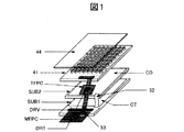
図1は、従来例1のタッチパネル付き液晶表示装置の概略構成を示す分解斜視図である。
図2は、図1に示すタッチパネルの電極構成を示す平面図である。
図3は、図1に示すタッチパネルの断面構造を示す断面図である。
一般的に、タッチパネルは、図2に示すように、容量検出用の走査電極(TX)と、検出電極(RX)を有する。ここでは、例えば、走査電極(TX)を3本(TX1〜TX3)、検出電極(RX)を2本(RX1,RX2)で図示しているが、電極数はこれに限らない。
また、タッチパネルは、図1、図3に示すように、タッチパネル基板41と、タッチパネル基板41上に形成される走査電極(TX)および検出電極(RX)と、走査電極(TX)および検出電極(RX)上に形成される層間絶縁膜42と、層間絶縁膜42上に形成され、走査電極(TX)同士を電気的に接続する接続部(STX)と、前記接続部(STX)上に形成される保護膜43と、前記保護膜43上に配置されるフロントウィンドウ(又は、保護フィルム)44と、前記タッチパネル基板41の液晶表示パネル側に形成されるシールド用の透明電極(例えば、ITO(Indium Tin Oxide)膜で形成される電極)45とで構成される。
従来のタッチパネルでは、タッチパネル制御IC(DRT)により、各走査電極(TX)を5V〜10V程度の電圧でパルス駆動を行い、タッチパネル制御IC(DRT)において、検出電極(RX)での電圧変化を検出し、タッチ位置の検出を行う。即ち、指等により走査電極(TX)と検出電極(RX)との間の容量値が変化し、走査電極(TX)をパルス駆動した際に、検出電極(RX)で検出される電圧変動が変化することから、検出電極(RX)の電圧を測定することによりタッチ位置を検出することができる。
Hereinafter, embodiments of the present invention will be described in detail with reference to the drawings.
In all the drawings for explaining the embodiments, parts having the same functions are given the same reference numerals, and repeated explanation thereof is omitted. Also, the following examples are not intended to limit the interpretation of the scope of the claims of the present invention.
[Conventional example 1]
FIG. 1 is an exploded perspective view showing a schematic configuration of a liquid crystal display device with a touch panel of Conventional Example 1. FIG.
FIG. 2 is a plan view showing an electrode configuration of the touch panel shown in FIG.
3 is a cross-sectional view showing a cross-sectional structure of the touch panel shown in FIG.
In general, as shown in FIG. 2, the touch panel includes a scanning electrode (TX) for detecting capacitance and a detection electrode (RX). Here, for example, three scanning electrodes (TX) (TX1 to TX3) and two detection electrodes (RX) (RX1 and RX2) are illustrated, but the number of electrodes is not limited thereto.
1 and 3, the touch panel includes a
In the conventional touch panel, each scanning electrode (TX) is pulse-driven with a voltage of about 5V to 10V by a touch panel control IC (DRT), and the voltage change at the detection electrode (RX) is detected in the touch panel control IC (DRT). Detect the touch position. That is, the capacitance value between the scan electrode (TX) and the detection electrode (RX) is changed by a finger or the like, and voltage fluctuation detected by the detection electrode (RX) when the scan electrode (TX) is pulse-driven. Since it changes, the touch position can be detected by measuring the voltage of the detection electrode (RX).
タッチパネルは、液晶表示パネルの前面に設置される。従って、液晶表示パネルに表示された画像を使用者が見る場合には、表示画像がタッチパネルを透過する必要があるため、タッチパネルは光透過率が高いことが望ましい。
液晶表示パネルは、図1に示すように、第1基板(SUB1;以下、TFT基板という)、第2基板(SUB2;以下、CF基板という)と、TFT基板(SUB1)とCF基板(SUB2)との間に挟持される液晶(図示せず)とを有する。
また、TFT基板(SUB1)は、CF基板(SUB2)よりも大きな面積を有し、TFT基板(SUB1)の、CF基板(SUB2)と対向しない領域には、液晶ドライバIC(DRV)が実装され、さらに、当該領域の一辺の周辺部には、メインフレキシブル配線基板(MFPC)が実装される。
なお、図1において、CTは対向電極(共通電極ともいう)、TFPCはタッチパネル用フレキシブル配線基板、CDは裏面側透明導電膜、52は接続部材、53は接続用フレキシブル配線基板である。
IPS方式の液晶表示パネルは、TN方式の液晶表示パネルやVA方式の液晶表示パネルのように、カラーフィルタが設けられる基板上に対向電極(CT)が存在しない。そのため、表示ノイズを低減する等の理由により、カラーフィルタが設けられる基板上に、例えばITOなどの透明導電膜で構成される裏面側透明導電膜(CD)が形成されている。
The touch panel is installed on the front surface of the liquid crystal display panel. Therefore, when a user views an image displayed on the liquid crystal display panel, the display image needs to pass through the touch panel, and thus it is desirable that the touch panel has high light transmittance.
As shown in FIG. 1, the liquid crystal display panel includes a first substrate (SUB1; hereinafter referred to as a TFT substrate), a second substrate (SUB2; hereinafter referred to as a CF substrate), a TFT substrate (SUB1) and a CF substrate (SUB2). Liquid crystal (not shown) sandwiched between the two.
Further, the TFT substrate (SUB1) has a larger area than the CF substrate (SUB2), and a liquid crystal driver IC (DRV) is mounted on a region of the TFT substrate (SUB1) that does not face the CF substrate (SUB2). Further, a main flexible wiring board (MFPC) is mounted on the periphery of one side of the area.
In FIG. 1, CT is a counter electrode (also referred to as a common electrode), TFPC is a touch panel flexible wiring board, CD is a back side transparent conductive film, 52 is a connection member, and 53 is a connection flexible wiring board.
Unlike the TN liquid crystal display panel and the VA liquid crystal display panel, the IPS liquid crystal display panel does not have a counter electrode (CT) on a substrate on which a color filter is provided. Therefore, for reasons such as reducing display noise, a back side transparent conductive film (CD) made of a transparent conductive film such as ITO is formed on a substrate on which a color filter is provided.
図4は、液晶表示パネルの内部にタッチパネルを内蔵したタッチパネル内蔵液晶表示装置の概略構成を示す分解斜視図である。
図4において、2はTFT基板、3はCF基板と、21は対向電極(共通電極ともいう)、5は液晶ドライバIC、MFPCはメインフレキシブル配線基板、40はフロントウィンドウ、53は接続用フレキシブル配線基板である。
図4に示す液晶表示装置では、CF基板3上の裏面側透明導電膜(CD)を、帯状のパターンに分割して、タッチパネルの検出電極31となし、TFT基板2の内部に形成される対向電極21を帯状のパターンに分割、即ち、複数のブロックに分割して、タッチパネルの走査電極として兼用することにより、タッチパネル基板(図1の41)を削減している。そのため、図4に示す液晶表示装置では、図1に示すタッチパネル制御IC(DRT)の機能が、液晶ドライバIC5の内部に設けられる。
FIG. 4 is an exploded perspective view showing a schematic configuration of a liquid crystal display device with a built-in touch panel in which a touch panel is built in the liquid crystal display panel.
In FIG. 4, 2 is a TFT substrate, 3 is a CF substrate, 21 is a counter electrode (also referred to as a common electrode), 5 is a liquid crystal driver IC, MFPC is a main flexible wiring substrate, 40 is a front window, and 53 is a flexible wiring for connection. It is a substrate.
In the liquid crystal display device shown in FIG. 4, the back-side transparent conductive film (CD) on the
次に、図5を用いて、図4に示す液晶表示装置の対向電極21と検出電極31について説明する。
前述したように、対向電極21はTFT基板2上に設けられているが、複数本の(例えば20本程度)対向電極21が両端で共通に接続され、対向電極信号線22と接続されている。
図5に示す液晶表示装置では、束状の対向電極21が走査電極(TX)を兼用し、また、検出電極31が検出電極(RX)を構成する。
したがって、対向電極信号には、画像表示に用いられる対向電圧と、タッチ位置の検出に用いられるタッチパネル走査電圧とが含まれる。タッチパネル走査電圧が対向電極21に印加されると、対向電極21と一定の間隔を持って配置され容量を構成する検出電極31に検出信号が生じる。この検出信号は検出電極用端子36を介して外部に取り出される。
なお、検出電極31の両側にはダミー電極33が形成されている。検出電極31は一方の端部でダミー電極33側に向かい広がりT字状の検出電極用端子36を形成している。 また、TFT基板2には対向電極信号線22以外にも駆動回路用入力端子25のような様々な配線、端子等が形成される。
Next, the
As described above, the
In the liquid crystal display device shown in FIG. 5, the bundled
Therefore, the counter electrode signal includes a counter voltage used for image display and a touch panel scanning voltage used for detecting the touch position. When the touch panel scanning voltage is applied to the
Note that
図4に示す液晶表示装置における、表示部の断面の一部を拡大した概略断面図を図6に示す。
図6に示すようにTFT基板2には画素部200が設けられており、対向電極21は画素の一部として画像表示に用いられる。また、TFT基板2とCF基板3との間には液晶組成物4が狭持されている。CF基板3に設けられた検出電極31とTFT基板に設けられた対向電極21とは容量を形成しており、対向電極21に駆動信号が印加されると検出電極31の電圧が変化する。
この時、図6に示すように、フロントウィンドウ40を介して指502等の導電体が近接または接触すると、容量に変化が生じ検出電極31に生じる電圧に、近接・接触が無い場合に比較して変化が生じる。
このように、液晶表示パネルに形成した対向電極21と検出電極31との間に生じる容量の変化を検出することで、液晶表示パネルにタッチパネルの機能を備えることが可能となる。
FIG. 6 shows a schematic cross-sectional view in which a part of the cross section of the display portion in the liquid crystal display device shown in FIG.
As shown in FIG. 6, the
At this time, as shown in FIG. 6, when a conductor such as a
Thus, by detecting a change in capacitance generated between the
図7は、本発明が適用される液晶表示装置の一例の、複数のブロックに分割した対向電極の一例を示す平面図である。図7において、SUB1はTFT基板、DRVは液晶ドライバIC、CT1〜CT20は帯状のパターンに分割された各ブロックの対向電極、GESは液晶表示パネルに内蔵された走査線駆動回路、CTLは対向電極配線、TAMはメインフレキシブル配線基板(MFPC)と接続される端子部、ARはマトリクス状に配置された複数の画素で構成される表示部である。
静電容量方式のタッチパネルでは、指等による静電容量の変化を検出するため、交流駆動を行うタッチパネル用の走査電極(TX)の幅は約4〜5mm程度の幅があることが望ましい。そのため、液晶表示パネルの大型化により走査電極(TX)の本数は増加する。
図7に示す例では、1280表示ラインの対向電極(CT)を、CT1〜CT20の20ブロック(1ブロックは64表示ラインの対向電極で構成される)に分割しており、対向電極配線(CTL)は左右に各20本必要となる。
各ブロックの対向電極(CT1〜CT20)は、表示動作において寄生容量により電圧変動した場合は画質悪化を引き起こす。そのため、各々のブロックの対向電極(CT1〜CT20)と、液晶ドライバIC(DRV)とを接続する対向電極配線(CTL)の抵抗値を下げる必要があるため、液晶表示パネルの大型化に伴い、対向電極(CT)の分割数が増加すると、対向電極配線(CTL)の配線領域が増加し、結果として、液晶表示パネルに左右の額縁の幅が増加することになる。
FIG. 7 is a plan view showing an example of the counter electrode divided into a plurality of blocks, which is an example of the liquid crystal display device to which the present invention is applied. In FIG. 7, SUB1 is a TFT substrate, DRV is a liquid crystal driver IC, CT1 to CT20 are counter electrodes of each block divided into strip-like patterns, GES is a scanning line driving circuit built in the liquid crystal display panel, and CTL is a counter electrode Wiring, TAM is a terminal portion connected to the main flexible wiring board (MFP), and AR is a display portion composed of a plurality of pixels arranged in a matrix.
In a capacitive touch panel, it is desirable that the width of the scanning electrode (TX) for touch panel for AC driving is about 4 to 5 mm in order to detect a change in capacitance due to a finger or the like. For this reason, the number of scanning electrodes (TX) increases as the liquid crystal display panel becomes larger.
In the example shown in FIG. 7, the counter electrode (CT) of the 1280 display lines is divided into 20 blocks CT1 to CT20 (one block is composed of counter electrodes of 64 display lines), and the counter electrode wiring (CTL) ) Requires 20 each on the left and right.
The counter electrodes (CT1 to CT20) of each block cause image quality deterioration when the voltage fluctuates due to parasitic capacitance in the display operation. Therefore, it is necessary to reduce the resistance value of the counter electrode wiring (CTL) that connects the counter electrode (CT1 to CT20) of each block and the liquid crystal driver IC (DRV). When the number of divisions of the counter electrode (CT) increases, the wiring area of the counter electrode wiring (CTL) increases, and as a result, the width of the left and right frame on the liquid crystal display panel increases.
図8は、本発明が適用される液晶表示装置の他の例の、複数のブロックに分割した対向電極の駆動方法を説明するための平面図である。
図8に示す液晶表示装置は、20ブロックに分割した各々の対向電極(CT1〜CT20)を、アドレスデコード方式により選択する対向電極選択回路(CTSC)を、液晶表示パネルの内部に内蔵した点で、図7に示す液晶表示装置と相違する。
20ブロックに分割した対向電極(CT1〜CT20)の選択方法をアドレスデコード方式とすることにより、低抵抗が必要となる配線は、対向電極(CT1〜CT20)に供給する対向電圧(Vcom)と、タッチパネル走査電圧(Vstc)の2本となる。
本実施例では、タッチパネル走査電圧(Vstc)は、対向電圧(Vcom)に対して、5〜10V高い電圧を直流で供給し、アドレス信号線(Saddres)を介して供給されるアドレス信号(addres)により走査箇所の選択を行い、タッチパネル走査信号(STC)に従い、走査電極(TX)を兼ねる、選択されたブロックの対向電極(CT)に対して、対向電圧(Vcom)、あるいは、タッチパネル走査電圧(Vstc)を切り替えて出力する。
対向電極(CT)の分割数が増加した場合でも、増加する配線は、アドレス信号線(Saddres)のみであり、液晶表示パネルの左右の額縁の増加を抑制したまま、タッチパネル走査電極として使用する対向電極の分割数を増加させることが可能となる。
FIG. 8 is a plan view for explaining a driving method of the counter electrode divided into a plurality of blocks in another example of the liquid crystal display device to which the present invention is applied.
The liquid crystal display device shown in FIG. 8 includes a counter electrode selection circuit (CTSC) that selects each counter electrode (CT1 to CT20) divided into 20 blocks by an address decoding method in the liquid crystal display panel. This is different from the liquid crystal display device shown in FIG.
By using the address decoding method as the selection method of the counter electrodes (CT1 to CT20) divided into 20 blocks, the wiring that requires a low resistance includes the counter voltage (Vcom) supplied to the counter electrodes (CT1 to CT20), and The touch panel scanning voltage (Vstc) is two.
In the present embodiment, the touch panel scanning voltage (Vstc) is a voltage that is 5 to 10 V higher than the counter voltage (Vcom) by a direct current, and is supplied via an address signal line (Saddres). In accordance with the touch panel scanning signal (STC), the counter voltage (Vcom) or the touch panel scanning voltage (CT) is selected for the counter electrode (CT) of the selected block that also serves as the scanning electrode (TX). Vstc) is switched and output.
Even when the number of divisions of the counter electrode (CT) increases, the only wiring that increases is the address signal line (Saddres), and the counter electrode used as the touch panel scan electrode while suppressing an increase in the left and right picture frames of the liquid crystal display panel. It is possible to increase the number of divided electrodes.
図9は、図8に示す対向電極選択回路(CTSC)の構成例を示すブロック図である。図9に示すように、対向電極選択回路(CTSC)は、DEC1〜DEC20のアドレスデコーダ回路と、SCH1〜SCH20の選択回路で構成されている。
図8に示す液晶表示装置では、タッチパネルの走査電極(TX)が5mmピッチとなるように、64表示ライン分の対向電極(CT)を、液晶表示パネルの内部で電気的に接続して1つのブロックとし、1280の表示ラインを20分割する。そして、当該20分割された対向電極(CT1〜CT20)と、アドレスデコーダ回路(DEC1〜DEC20)とを、1対1で割りつけている。分割数が、20ブロックであるため、アドレス信号線(Sadd)は5bitの5本が必要となる。
アドレス信号(addres)により選択された、1ブロックの対向電極、即ち、64表示ライン分の対向電極(CT)が、タッチパネル走査信号(STC)により交流駆動を行い、その他の対向電極(CT)は対向電圧を出力する。
FIG. 9 is a block diagram showing a configuration example of the counter electrode selection circuit (CTSC) shown in FIG. As shown in FIG. 9, the counter electrode selection circuit (CTSC) includes an address decoder circuit of DEC1 to DEC20 and a selection circuit of SCH1 to SCH20.
In the liquid crystal display device shown in FIG. 8, the counter electrodes (CT) for 64 display lines are electrically connected inside the liquid crystal display panel so that the scanning electrodes (TX) of the touch panel have a pitch of 5 mm. The 1280 display lines are divided into 20 blocks. The 20 divided counter electrodes (CT1 to CT20) and the address decoder circuits (DEC1 to DEC20) are assigned one to one. Since the number of divisions is 20 blocks, five address signal lines (Sadd) are required.
One block of the counter electrode selected by the address signal (addres), that is, the counter electrode (CT) for 64 display lines is AC driven by the touch panel scanning signal (STC), and the other counter electrode (CT) is Outputs counter voltage.
図10は、図9に示す選択回路(SCH1〜SCH20)の一例の回路構成を示す回路図である。
図10に示す選択回路は、アドレスデコーダ回路(DEC1〜DEC20)の出力(DECO)と、インバータ(INV1)で反転されたタッチパネル走査信号(STC)の反転信号とを、ノア回路(NOR1)に入力し、当該ノア回路(NOR1)の出力をインバータ(INV2)で反転して、スイッチ回路(SW)に入力することにより、タッチパネル走査電圧(Vstc)、あるいは、対向電圧(Vcom)を選択して各ブロックの対向電極(CT1〜CT20)に出力する。
これにより、アドレスデコーダ回路(DEC1〜DEC20)の一つが選択された場合、タッチパネル走査信号(STC)に従い、各ブロックの対向電極に、タッチパネル走査電圧(Vstc)と、対向電圧(Vcom)とを切り替えて出力する。
即ち、図8に示す選択回路では、アドレスデコーダ回路(DEC1〜DEC20)の出力(DECO)が、Lowレベル(以下、Lレベル)、および、タッチパネル走査信号(STC)がHighレベル(以下、Hレベル)のときに、ノア回路(NOR1)の出力がHレベルとなるので、スイッチ回路(SW)は、タッチパネル走査電圧(Vstc)を選択し、タッチパネル走査信号(STC)がLレベル、あるいは、アドレスデコーダ回路(DEC1〜DEC20)の出力(DECO)が、Hレベルのときに、ノア回路(NOR1)の出力がLレベルとなるので、スイッチ回路(SW)は、対向電圧(Vcom)を選択する。
FIG. 10 is a circuit diagram showing a circuit configuration of an example of the selection circuits (SCH1 to SCH20) shown in FIG.
The selection circuit shown in FIG. 10 inputs the output (DECO) of the address decoder circuit (DEC1 to DEC20) and the inverted signal of the touch panel scanning signal (STC) inverted by the inverter (INV1) to the NOR circuit (NOR1). Then, the output of the NOR circuit (NOR1) is inverted by the inverter (INV2) and input to the switch circuit (SW) to select the touch panel scanning voltage (Vstc) or the counter voltage (Vcom). It outputs to the counter electrode (CT1-CT20) of a block.
Thereby, when one of the address decoder circuits (DEC1 to DEC20) is selected, the touch panel scanning voltage (Vstc) and the counter voltage (Vcom) are switched to the counter electrode of each block according to the touch panel scanning signal (STC). Output.
That is, in the selection circuit shown in FIG. 8, the output (DECO) of the address decoder circuit (DEC1 to DEC20) is low level (hereinafter referred to as L level), and the touch panel scanning signal (STC) is high level (hereinafter referred to as H level). ), The output of the NOR circuit (NOR1) becomes H level, so that the switch circuit (SW) selects the touch panel scanning voltage (Vstc) and the touch panel scanning signal (STC) is at L level or the address decoder. When the outputs (DECO) of the circuits (DEC1 to DEC20) are at the H level, the output of the NOR circuit (NOR1) is at the L level, so that the switch circuit (SW) selects the counter voltage (Vcom).
図11は、図7に示すアドレスデコーダ回路(DEC1〜DEC20)の一例の回路構成を示す回路図である。
図11に示すように、アドレスデコーダ回路(DEC1〜DEC20)には、5個のアドレス信号(addres)の各々について、アドレス信号、あるいは、アドレス信号をインバータ(INV)で反転した反転信号が入力され、5個のアドレス信号(addres)と5個のアドレス信号(addres)の反転信号の組み合わせに基づきデコードする。
図11に示すアドレスデコーダ回路では、アドレスデコーダ回路に入力された5個のアドレス信号(addres)と5個のアドレス信号(addres)の反転信号の中の所定の組み合わせのアドレス信号(add)をナンド回路(NAND1,NAND2)に入力し、当該ナンド回路(NAND1,NAND2)の出力を、ノア回路(NOR2)に入力し、当該ノア回路(NOR2)の出力をインバータ(INV3)で反転して、アドレスデコーダ回路の出力(DECO)としている。したがって、図11に示すアドレスデコーダ回路では、アドレス信号の組み合わせが、自アドレスデコーダ回路に設定されたアドレス信号の組み合わせと一致するときに、Lレベルの電圧が、アドレスデコーダ回路の出力(DECO)として出力され、アドレス信号の組み合わせが、自アドレスデコーダ回路に設定されたアドレス信号の組み合わせと一致しないときに、Hレベルの電圧が、アドレスデコーダ回路の出力(DECO)として出力される。
FIG. 11 is a circuit diagram showing a circuit configuration of an example of the address decoder circuit (DEC1 to DEC20) shown in FIG.
As shown in FIG. 11, the address decoder circuit (DEC1 to DEC20) receives an address signal or an inverted signal obtained by inverting the address signal with an inverter (INV) for each of the five address signals (addresses). Decoding is performed based on a combination of five address signals (addres) and an inverted signal of the five address signals (addres).
In the address decoder circuit shown in FIG. 11, an address signal (add) of a predetermined combination among five address signals (addres) and an inverted signal of five address signals (addres) input to the address decoder circuit is NANDed. The input to the circuit (NAND1, NAND2), the output of the NAND circuit (NAND1, NAND2) is input to the NOR circuit (NOR2), the output of the NOR circuit (NOR2) is inverted by the inverter (INV3), and the address The output (DECO) of the decoder circuit is used. Therefore, in the address decoder circuit shown in FIG. 11, when the combination of address signals matches the combination of address signals set in the self-address decoder circuit, the L level voltage is used as the output (DECO) of the address decoder circuit. When the combination of the output address signals does not match the combination of the address signals set in the self-address decoder circuit, an H level voltage is output as the output (DECO) of the address decoder circuit.
図12は、タッチパネル内蔵液晶表示装置における、タッチパネル検出時と、画素書込み時の駆動波形を説明するための図である。
図12のAは、20ブロックに分割された対向電極のうち、11番目のブロックとなる641〜704表示ラインの対向電極(CT11)に供給されるタッチパネル走査電圧(Vstc)の電圧波形を示している。また、図12のBは、奇数列の映像線(DL)に供給される映像電圧の波形を、図12のCは、偶数列の映像線(DL)に供給される映像電圧の波形を、図12のDは、641番目の走査線(GL)を介して、641表示ラインの薄膜トランジスタのゲート電極に供給されるゲート信号を示している。さらに、T1は、タッチ位置検出期間、T2は画素書込み期間を示している。
タッチ位置検出期間(T1)は、表示への影響を防止するため、画素書込み期間(T2)以外の期間に設定される。また、タッチ位置検出期間(T1)において、検出感度を増加させるために、同一箇所の走査電極(TX)で複数回のスキャン、即ち、図12では、11番目のブロックの対向電極(CT11)に、複数回タッチパネル走査電圧(Vstc)が供給される。また、画素書き込み期間(T2)内には、11番目のブロックの対向電極(CT11)には、タッチパネル走査電圧(Vstc)が供給されず、対向電圧(Vcom)が供給される。
FIG. 12 is a diagram for explaining driving waveforms at the time of touch panel detection and pixel writing in the liquid crystal display device with a built-in touch panel.
FIG. 12A shows the voltage waveform of the touch panel scanning voltage (Vstc) supplied to the counter electrode (CT11) of the 641-704 display line that is the eleventh block among the counter electrodes divided into 20 blocks. Yes. 12B shows the waveform of the video voltage supplied to the odd-numbered video lines (DL), and FIG. 12C shows the waveform of the video voltage supplied to the even-numbered video lines (DL). D of FIG. 12 shows a gate signal supplied to the gate electrode of the thin film transistor of the 641 display line through the 641st scanning line (GL). Further, T1 represents a touch position detection period, and T2 represents a pixel writing period.
The touch position detection period (T1) is set to a period other than the pixel writing period (T2) in order to prevent the influence on the display. Further, in order to increase the detection sensitivity in the touch position detection period (T1), the scan electrode (TX) at the same location is scanned a plurality of times, that is, in the counter electrode (CT11) of the eleventh block in FIG. The touch panel scanning voltage (Vstc) is supplied a plurality of times. In the pixel writing period (T2), the counter electrode (CT11) of the eleventh block is not supplied with the touch panel scanning voltage (Vstc) but supplied with the counter voltage (Vcom).
図13は、タッチパネル内蔵液晶表示装置における、タッチパネル検出時と、画素書込み時のタイミングを説明するための図である。
図13のAは、1フレームの画素書込み期間(T4)に、1番目の表示ラインから1280表示ラインまでの画素書込みタイミングを示し、図13のBが、20ブロックに分割された各ブロックの対向電極(CT1〜CT20)におけるタッチパネル検出タイミングを示す。
図13に示すように、任意の表示ラインの対向電極を走査電極(TX)として機能させ、タッチパネル検出時のスキャン動作は、画素書き込みを行うゲートスキャンとは異なる箇所で行う。なお、図13において、T3は帰線期間、VSYNCは垂直同期信号、HSYNCは水平同期信号を示す。
FIG. 13 is a diagram for explaining the timing when the touch panel is detected and when the pixel is written in the liquid crystal display device with a built-in touch panel.
13A shows the pixel writing timing from the first display line to the 1280 display line in the pixel writing period (T4) of one frame, and FIG. 13B shows the opposite of each block divided into 20 blocks. The touch panel detection timing in an electrode (CT1-CT20) is shown.
As shown in FIG. 13, the counter electrode of an arbitrary display line is made to function as a scanning electrode (TX), and the scanning operation at the time of touch panel detection is performed at a location different from the gate scanning for pixel writing. In FIG. 13, T3 represents a blanking period, VSYNC represents a vertical synchronization signal, and HSYNC represents a horizontal synchronization signal.
図14は、タッチパネル内蔵液晶表示装置における、1水平走査期間の映像電圧と、走査電圧と、タッチパネル走査タイミングを示す図である。
図13で説明したように、ゲートスキャン(図14のA)と、タッチパネル走査(図14のB)は異なる表示ラインで実施しているが、映像線と、対向電極(CT)との間には寄生容量があるため、映像線上の電圧(VDL)が変動することに生じるノイズ(図14のNz1と、Nz3)により、タッチパネル走査電圧(Vstc)の立ち上がり波形に歪みが生じると、検出電極(図4の31)への検出電流が少なくなり検出感度が低下する。
同様に、走査線と、対向電極(CT)との間には寄生容量があるため、選択走査電圧(VGL)の立ち上がり、あるいは、立ち下り時に生じるノイズ(図14のNz2と、Nz4)により、タッチパネル走査電圧(Vstc)の立ち上がり波形に歪みが生じると、検出電極(図4の31)への検出電流が少なくなり検出感度が低下する。
また、対向電極配線(CTL)の抵抗により、対向電極配線(CTL)の遠端で、タッチパネル走査電圧(Vstc)のパルス幅の縮小が生じた場合にも検出感度が低下する。
そこで、本実施例では、液晶ドライバIC(DRV)が、タッチパネル走査電圧(Vstc)の立ち上がりタイミングと、パルス幅を調整する機能を内蔵している。
タッチパネル走査電圧(Vstc)の立ち上がりタイミングと、パルス幅の調整は、液晶ドライバIC(DRV)の内部に設けられるタイミング設定レジスタと走査パルス幅レジスタを使用して実行される。
FIG. 14 is a diagram illustrating a video voltage, a scanning voltage, and a touch panel scanning timing in one horizontal scanning period in the liquid crystal display device with a touch panel.
As described in FIG. 13, the gate scan (A in FIG. 14) and the touch panel scan (B in FIG. 14) are performed on different display lines, but between the video line and the counter electrode (CT). Since there is a parasitic capacitance, if the rising waveform of the touch panel scanning voltage (Vstc) is distorted due to noise (Nz1 and Nz3 in FIG. 14) generated when the voltage (VDL) on the video line fluctuates, the detection electrode ( The detection current to 31) in FIG. 4 is reduced and the detection sensitivity is lowered.
Similarly, since there is a parasitic capacitance between the scanning line and the counter electrode (CT), noise (Nz2 and Nz4 in FIG. 14) generated at the rising or falling of the selected scanning voltage (VGL) When the rising waveform of the touch panel scanning voltage (Vstc) is distorted, the detection current to the detection electrode (31 in FIG. 4) decreases and the detection sensitivity decreases.
The detection sensitivity also decreases when the pulse width of the touch panel scanning voltage (Vstc) is reduced at the far end of the counter electrode wiring (CTL) due to the resistance of the counter electrode wiring (CTL).
Therefore, in this embodiment, the liquid crystal driver IC (DRV) has a function of adjusting the rising timing of the touch panel scanning voltage (Vstc) and the pulse width.
The rise timing of the touch panel scanning voltage (Vstc) and the adjustment of the pulse width are executed using a timing setting register and a scanning pulse width register provided in the liquid crystal driver IC (DRV).
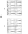
図15は、本発明の実施例のタイミング設定レジスタと走査パルス幅レジスタの一例の仕様を示す図である。
図16は、本発明の実施例の液晶表示装置における、1水平走査期間の映像電圧と、走査電圧と、タッチパネル走査タイミングの一例を示す図である。
図15(a)に示すように、タイミング設定レジスタに設定されたデータにより、1水平走査期間の基準時点からタッチパネル走査電圧(Vstc)の立ち上がりタイミング(図16のDELAY)が、0.5us刻みで自由に調節可能である。
これにより、図16に示すように、液晶表示パネル毎に、1水平走査期間内における、タッチパネル走査電圧(Vstc)の立ち上がりタイミングを、映像線上の映像電圧(VDL)の電圧遷移タイミングと、選択走査電圧(VGL)の立ち上がり、あるいは、立ち下り時から自由にずらすことができる。
なお、基準位置は、映像線上の映像電圧(VDL)の電圧変動タイミング、あるいは、選択走査電圧(VGL)の立ち上がり、あるいは、立ち下り時点とされる。
さらに、図15(a)に示す走査パルス幅レジスタに設定されたデータにより、タッチパネル走査電圧(Vstc)のパルス幅(図16のWIDTH)を、0.5us刻みで自由に調節可能である。
これにより、液晶表示パネル毎に、1水平走査期間内における、タッチパネル走査電圧(Vstc)のパルス幅を自由に設定できるため、走査線駆動回路(GES)が、半導体層がアモルファスシリコン(a−Si)で構成される薄膜トランジスタ(a−Si TFT)や、あるいは、半導体層がポリシリコン(p−Si)で構成される薄膜トランジスタ(p−Si TFT)等の、対向電極(CT)に対向電圧(Vcom)を供給する対向電極配線(CTL)の配線負荷が異なる液晶表示パネルでも、検出感度について、それぞれの配線負荷に応じた最適な設定をすることができる。
FIG. 15 is a diagram showing specifications of an example of the timing setting register and the scan pulse width register according to the embodiment of the present invention.
FIG. 16 is a diagram illustrating an example of the video voltage, the scanning voltage, and the touch panel scanning timing in one horizontal scanning period in the liquid crystal display device according to the embodiment of the present invention.
As shown in FIG. 15A, the rising timing (DELAY in FIG. 16) of the touch panel scanning voltage (Vstc) from the reference time point in one horizontal scanning period is incremented by 0.5 us by the data set in the timing setting register. It is freely adjustable.
Thus, as shown in FIG. 16, for each liquid crystal display panel, the rising timing of the touch panel scanning voltage (Vstc), the voltage transition timing of the video voltage (VDL) on the video line, and the selective scanning within one horizontal scanning period. The voltage (VGL) can be freely shifted from the rising or falling time.
Note that the reference position is the voltage fluctuation timing of the video voltage (VDL) on the video line, or the rising or falling time of the selected scanning voltage (VGL).
Furthermore, the pulse width (WIDTH in FIG. 16) of the touch panel scanning voltage (Vstc) can be freely adjusted in steps of 0.5 us by data set in the scanning pulse width register shown in FIG.
Accordingly, since the pulse width of the touch panel scanning voltage (Vstc) can be freely set for each liquid crystal display panel within one horizontal scanning period, the scanning line driving circuit (GES) has an amorphous silicon (a-Si) semiconductor layer. ) Or a thin film transistor (p-Si TFT) in which the semiconductor layer is made of polysilicon (p-Si) or the like, the counter voltage (Vcom) In the liquid crystal display panel in which the wiring load of the counter electrode wiring (CTL) for supplying the same is different, the detection sensitivity can be optimally set according to each wiring load.
このように、タイミング設定レジスタと走査パルス幅レジスタに、最適な遅延量となるデータを書き込みことにより、ゲートスキャンからのタッチパネル走査へのノイズの干渉を防止し、対向電極配線(CTL)の配線負荷の異なる液晶表示パネルの検出感度を最適に設定できるようにした。
タッチパネル内蔵液晶表示装置では、タッチパネル用の走査電極(TX)を、TFT基板(SUB1;TFT基板)上の対向電極(CT)を分割し、タッチパネル用の走査電極として兼用して使用している。
本実施例のように、液晶ドライバIC(DRV)が、タッチパネル走査電圧(Vstc)の立ち上がりタイミングを調整する機能を内蔵することにより、表示動作によるノイズ発生タイミングから、タッチパネル走査電圧(Vstc)の立ち上がりタイミングをずらすことができ、ノイズの干渉を防止することができる。
また、本実施例のように、液晶ドライバIC(DRV)が、タッチパネル走査電圧(Vstc)のパルス幅調整機能を内蔵することにより、対向電極配線(CTL)の配線負荷が異なる液晶表示パネルでも、検出感度についてそれぞれの配線負荷に応じた最適な設定をすることができる。これらのタイミング調整機能によりタッチ検出感度の向上が可能となる。
In this way, by writing the data with the optimum delay amount to the timing setting register and the scan pulse width register, interference of noise from the gate scan to the touch panel scan is prevented, and the wiring load of the counter electrode wiring (CTL) The detection sensitivity of different LCD panels can be set optimally.
In the liquid crystal display device with a built-in touch panel, the scanning electrode (TX) for the touch panel is divided and used as the scanning electrode for the touch panel by dividing the counter electrode (CT) on the TFT substrate (SUB1; TFT substrate).
As in this embodiment, the liquid crystal driver IC (DRV) has a function of adjusting the rising timing of the touch panel scanning voltage (Vstc), so that the rising edge of the touch panel scanning voltage (Vstc) is detected from the timing of noise generation due to the display operation. Timing can be shifted and noise interference can be prevented.
Further, as in this embodiment, the liquid crystal driver IC (DRV) has a built-in function of adjusting the pulse width of the touch panel scanning voltage (Vstc). The detection sensitivity can be optimally set according to each wiring load. These timing adjustment functions can improve touch detection sensitivity.
タッチパネル走査電圧(Vstc)は、電圧振幅が大きい程、タッチパネル用の検出電極(Rx)に電流が多く流れるため検出感度が向上する。
検出感度の向上が必要な場合は、タッチパネル走査電圧(Vstc)を高く設定するが、液晶ドライバIC(DRV)のタッチパネル走査電圧(Vstc)の出力端子と、対向電圧(Vcom)の出力端子の耐圧が6Vのため、タッチパネル走査電圧(Vstc)と対向電圧(Vcom)との間の電位差は6V以下で使用しなければならない。
しかし、タッチパネル内蔵液晶表示装置では、対向電極(CT)が、タッチパネル用の走査電極(TX)を兼用しているため、タッチパネル走査電圧(Vstc)のLレベルの電圧は対向電圧(Vcom)であり、液晶表示パネル毎に電圧値が異なる。
特に、半導体層がポリシリコン(p−Si)で構成される薄膜トランジスタ(p−Si TFT)に比べて安価で作製できる、半導体層がアモルファスシリコン(a−Si)で構成される薄膜トランジスタ(a−Si TFT)を使用する液晶表示パネルは、液晶表示パネル毎のコモン電圧ばらつきが大きいため、タッチパネル走査電圧(Vstc)を固定値としていると6Vの耐圧を越えてしまう場合がある。
そこで、本実施例では、液晶ドライバIC(DRV)が、走査電圧パルス振幅設定レジスタを内蔵し、液晶表示パネル毎の対向電圧(Vcom)に対して、設定振幅電圧を加算したタッチパネル走査電圧(Vstc)を選択し、出力する機能を内蔵している。
As the voltage amplitude of the touch panel scanning voltage (Vstc) increases, the detection sensitivity improves because a larger amount of current flows through the detection electrode (Rx) for the touch panel.
When the detection sensitivity needs to be improved, the touch panel scanning voltage (Vstc) is set high, but the withstand voltage of the output terminal of the touch panel scanning voltage (Vstc) of the liquid crystal driver IC (DRV) and the output terminal of the counter voltage (Vcom). Therefore, the potential difference between the touch panel scanning voltage (Vstc) and the counter voltage (Vcom) must be 6V or less.
However, in the liquid crystal display device with a built-in touch panel, the counter electrode (CT) also serves as the scan electrode (TX) for the touch panel, so the L level voltage of the touch panel scan voltage (Vstc) is the counter voltage (Vcom). The voltage value is different for each liquid crystal display panel.
In particular, a thin film transistor (a-Si) whose semiconductor layer is made of amorphous silicon (a-Si) can be manufactured at a lower cost than a thin film transistor (p-Si TFT) whose semiconductor layer is made of polysilicon (p-Si). Since the liquid crystal display panel using TFT) has a large common voltage variation for each liquid crystal display panel, if the touch panel scanning voltage (Vstc) is set to a fixed value, the withstand voltage of 6 V may be exceeded.
Therefore, in this embodiment, the liquid crystal driver IC (DRV) has a built-in scanning voltage pulse amplitude setting register, and a touch panel scanning voltage (Vstc) obtained by adding the setting amplitude voltage to the counter voltage (Vcom) for each liquid crystal display panel. Built-in function to select and output.
図17に、従来の、液晶表示パネル毎の対向電圧(Vcom)に対して、設定振幅電圧を加算したタッチパネル走査電圧(Vstc)を出力する回路構成を示す。
図17に示す回路構成では、対向電圧生成回路113により生成した対向電圧(Vcom)と、走査電圧パルス幅生成回路111により生成したタッチパネル走査電圧振幅値(図16のAMP)を、オペアンプによる加算器112で加算して、タッチパネル走査電圧(Vstc)を生成している。
ここで、対向電圧生成回路113は、対向電圧レジスタ102に基づき対向電圧(Vcom)を生成し、走査電圧パルス幅生成回路111は、走査電圧パルス振幅設定レジスタ101に基づきタッチパネル走査電圧振幅値を生成する。
また、対向電圧レジスタ102には、外部から対向電圧(Vcom)を設定するためのデータ(VCOM[7:0])が設定され、対向電圧レジスタ102に設定された値に基づき、電子可変抵抗回路(DBR1)を制御し、対向電圧(Vcom)を、例えば、0.025V単位で調整可能となっている。
同様に、走査電圧パルス振幅設定レジスタ101には、外部からタッチパネル走査電圧振幅値(図16のAMP)を設定するためのデータ(AMP[3:0])が設定され、走査電圧パルス振幅設定レジスタ101に設定された値に基づき、電子可変抵抗回路(DBR2)を制御し、タッチパネル走査電圧振幅値(図16のAMP)を、例えば、0.2V単位で調整可能となっている。
また、図17において、アンプ回路(AMP1,AMP2,AMP4)はバッファ回路として動作し、アンプ回路(AMP3)は、利得1の電圧反転回路として動作する。さらに、図17において、Cvsは走査電圧安定化容量素子、CVmは対向電圧安定化容量素子、TAPは液晶ドライバIC(DRV)の出力端子である。
しかしながら、図17に示すアナログ回路を使用した方式では回路面積が大きいため、液晶ドライバIC(DRV)のチップサイズ増加になる。
FIG. 17 shows a conventional circuit configuration for outputting a touch panel scanning voltage (Vstc) obtained by adding a set amplitude voltage to a counter voltage (Vcom) for each liquid crystal display panel.
In the circuit configuration shown in FIG. 17, the counter voltage (Vcom) generated by the counter
Here, the counter
The
Similarly, data (AMP [3: 0]) for setting the touch panel scanning voltage amplitude value (AMP in FIG. 16) from the outside is set in the scanning voltage pulse
In FIG. 17, the amplifier circuits (AMP1, AMP2, AMP4) operate as a buffer circuit, and the amplifier circuit (AMP3) operates as a voltage inverting circuit with a gain of 1. Further, in FIG. 17, Cvs is a scanning voltage stabilization capacitor element, CVm is a counter voltage stabilization capacitor element, and TAP is an output terminal of a liquid crystal driver IC (DRV).
However, in the method using the analog circuit shown in FIG. 17, the circuit area is large, which increases the chip size of the liquid crystal driver IC (DRV).
図18は、本発明の実施例の、液晶表示パネル毎の対向電圧(Vcom)に対して、設定振幅電圧を加算したタッチパネル走査電圧(Vstc)を出力する回路構成を示す図である。
図19は、本発明の実施例の対向電圧設定レジスタ102と走査電圧パルス幅設定レジスタ101の一例の仕様を示す図である。
本実施例では、外部から入力され対向電圧設定レジスタ102に設定されたデータ(VCOM[7:0])と、外部から入力され走査電圧パルス幅設定レジスタ101に設定されたデータ(AMP[3:0])とを、論理演算回路103で論理演算し、当該論理演算回路103から出力されるデータ(SCAN[3:0])を、走査電圧設定レジスタ104に設定し、走査電圧設定レジスタ104に設定された値に基づき、電子可変抵抗回路(DBR2)を制御し、タッチパネル走査電圧(Vstc)を生成する。
なお、本実施例では、図19(c)に示すように、走査電圧設定レジスタ104に設定された値に基づき、タッチパネル走査電圧(Vstc)を、例えば、0.2V単位で調整可能となっている。
また、図19(b)に示すように、走査電圧パルス振幅設定レジスタ101に設定された値に基づき、タッチパネル走査電圧振幅値(図16のAMP)を、例えば、0.2V単位で調整可能となっている。
さらに、図19(a)に示すように、走査電圧設定レジスタ104に設定された値に基づき、タッチパネル走査電圧(Vstc)を、例えば、0.2V単位で調整可能となっている。
FIG. 18 is a diagram showing a circuit configuration for outputting a touch panel scanning voltage (Vstc) obtained by adding a set amplitude voltage to the counter voltage (Vcom) for each liquid crystal display panel according to the embodiment of the present invention.
FIG. 19 is a diagram showing specifications of an example of the counter
In this embodiment, data (VCOM [7: 0]) input from the outside and set in the counter
In this embodiment, as shown in FIG. 19C, the touch panel scanning voltage (Vstc) can be adjusted in units of 0.2 V, for example, based on the value set in the scanning
Further, as shown in FIG. 19B, based on the value set in the scanning voltage pulse
Further, as shown in FIG. 19A, the touch panel scanning voltage (Vstc) can be adjusted in units of 0.2V, for example, based on the value set in the scanning
本実施例では、図17に示すアナログ回路を使用した方式に代えて、デジタル回路を使用するようしたので、回路面積を縮小することができる。
図19(c)に示すように、走査電圧パルス幅設定レジスタ101により、タッチパネル走査電圧振幅値(図16のAMP)が6Vと設定した場合、対向電圧(Vcom)が0V〜−1Vの液晶表示パネルはタッチパネル走査電圧(Vstc)として5Vを選択し、対向電圧(Vcom)が−1.025〜−1.2Vの液晶表示パネルはタッチパネル走査電圧(Vstc)として4.8Vを選択する。
このようにして、液晶表示パネル毎に異なる対向電圧(Vcom)に対して、一定の振幅値のタッチパネル走査電圧(Vstc)を得ることができる。
このように、本実施例では、液晶ドライバIC(DRV)に、対向電圧(Vcom)に対して、タッチパネル走査電圧振幅値分、高いタッチパネル走査電圧(Vstc)を生成して、出力する機能を内蔵している。
液晶表示パネル毎に異なる対向電圧(Vcom)に対して、液晶表示パネル毎のタッチパネル走査電圧(Vstc)の振幅値を一定にすることができるため、液晶表示パネル毎のタッチの検出感度を均一にすることができる。さらに、タッチパネル走査電圧(Vstc)の振幅は小さく設定することもできるため低消費電力にすることもできる。
その上、この機能を、液晶ドライバIC(DRV)内部のロジック回路で実施することにより、アナログ回路で実施するよりも回路面積を縮小し、チップサイズ縮小による原価低減を図ることが可能である。
以上、本発明者によってなされた発明を、前記実施例に基づき具体的に説明したが、本発明は、前記実施例に限定されるものではなく、その要旨を逸脱しない範囲において種々変更可能であることは勿論である。
In this embodiment, since a digital circuit is used instead of the method using the analog circuit shown in FIG. 17, the circuit area can be reduced.
As shown in FIG. 19C, when the touch panel scanning voltage amplitude value (AMP in FIG. 16) is set to 6V by the scanning voltage pulse
In this manner, a touch panel scanning voltage (Vstc) having a constant amplitude value can be obtained with respect to the counter voltage (Vcom) that is different for each liquid crystal display panel.
As described above, in this embodiment, the liquid crystal driver IC (DRV) has a function of generating and outputting a touch panel scanning voltage (Vstc) that is higher by the touch panel scanning voltage amplitude value than the counter voltage (Vcom). doing.
Since the amplitude value of the touch panel scanning voltage (Vstc) for each liquid crystal display panel can be made constant with respect to the counter voltage (Vcom) that differs for each liquid crystal display panel, the touch detection sensitivity for each liquid crystal display panel is made uniform. can do. Furthermore, since the amplitude of the touch panel scanning voltage (Vstc) can be set small, the power consumption can be reduced.
In addition, by implementing this function in the logic circuit inside the liquid crystal driver IC (DRV), it is possible to reduce the circuit area and to reduce the cost by reducing the chip size, compared with the case where the function is implemented with an analog circuit.
As mentioned above, the invention made by the present inventor has been specifically described based on the above embodiments. However, the present invention is not limited to the above embodiments, and various modifications can be made without departing from the scope of the invention. Of course.
2,SUB1 第1基板
3,SUB2 第2基板
4 液晶組成物
5,DRV 液晶ドライバIC
21,CT,CT1〜CT20 対向電極
22 対向電極信号線
25 駆動回路用入力端子
31 検出電極
33 ダミー電極
36 検出電極用端子
40,44 フロントウィンドウ(又は、保護フィルム)
41 タッチパネル基板
42,PAS1,PAS2 層間絶縁膜
43 保護膜
45 シールド用の透明電極
52 接続部材
53 接続用フレキシブル配線基板
101 走査電圧パルス振幅設定レジスタ
102 対向電圧レジスタ
103 論理演算回路
104 走査電圧設定レジスタ
111 走査電圧パルス幅生成回路
112 加算器
113 対向電圧生成回路
200 画素部
502 指
TX タッチパネルの走査電極
RE タッチパネルの検出電極
AR 表示領域
DRT タッチパネル制御IC
MFPC メインフレキシブル配線基板
TFPC タッチパネル用フレキシブル配線基板
GES 走査線駆動回路
CTSC 対向電極選択回路
CTL 対向電極配線
CD 裏面側透明導電膜
DEC1〜DEC20 アドレスデコーダ回路
SCH1〜SCH20 選択回路
INV1〜INV3 インバータ
NOR1,NOR2 ノア回路
NAND1,NAND2 ナンド回路
SW スイッチ回路
STX 接続部
AMP1〜AMP4 アンプ回路
DBR1,DBR2 電子可変抵抗回路
Cvs 走査電圧安定化容量素子
CVm 対向電圧安定化容量素子
TAM メインフレキシブル配線基板(MFPC)と接続される端子部、
TAP 液晶ドライバIC(DRV)の出力端子
2, SUB1
21, CT, CT1 to
41
MFPC main flexible wiring board TFPC touch panel flexible wiring board GES scanning line drive circuit CTSC counter electrode selection circuit CTL counter electrode wiring CD back side transparent conductive film DEC1 to DEC20 address decoder circuits SCH1 to SCH20 selection circuits INV1 to INV3 inverter NOR1, NOR2 NOR Circuit NAND1, NAND2 NAND circuit SW Switch circuit STX Connection part AMP1-AMP4 Amplifier circuit DBR1, DBR2 Electronic variable resistance circuit Cvs Scanning voltage stabilization capacitor element CVm Opposite voltage stabilization capacitor element TAM Main flexible wiring board (MFPC) Terminal part,
Output terminal of TAP liquid crystal driver IC (DRV)
Claims (9)
第2基板と、
前記第1基板と前記第2基板との間に挟持される液晶とを有する液晶表示パネルを備え、マトリクス状に配置された複数の画素を有する液晶表示装置であって、
前記第2基板は、タッチパネルの検出電極を有し、
前記各画素は前記第1基板に形成され、画素電極と対向電極とを有し、
前記対向電極は、複数のブロックに分割されており、
前記分割された各ブロックの対向電極は、連続する複数の表示ラインの各画素に対して共通に設けられており、
前記分割された各ブロックの対向電極は、前記タッチパネルの走査電極を兼用し、
前記液晶表示パネルを駆動し、前記分割された各ブロックの対向電極に対して、対向電圧とタッチパネル走査電圧を供給する駆動回路を有し、
前記駆動回路は、前記対向電極に前記タッチパネル走査電圧を供給するタッチ位置検出期間を、前記画素に映像電圧を書き込む画素書込み期間以外の期間に設定し、前記タッチ位置検出期間に、前記タッチパネル走査電圧とは別のタッチパネル走査信号に従い、同じブロックの前記対向電極に対し連続して複数回、前記タッチパネル走査電圧を供給し、
前記駆動回路は、タイミング設定レジスタを有し、前記分割された各ブロックの対向電極に対して、順次供給する前記タッチパネル走査電圧の供給開始タイミングを前記タイミング設定レジスタに設定されたデータに基づき調整可能であることを特徴とする液晶表示装置。 A first substrate;
A second substrate;
A liquid crystal display device comprising a liquid crystal display panel having a liquid crystal sandwiched between the first substrate and the second substrate, and having a plurality of pixels arranged in a matrix,
The second substrate has a touch panel detection electrode;
Each of the pixels is formed on the first substrate and includes a pixel electrode and a counter electrode.
The counter electrode is divided into a plurality of blocks,
The counter electrode of each of the divided blocks is provided in common for each pixel of a plurality of continuous display lines,
The counter electrode of each divided block also serves as the scan electrode of the touch panel,
A driving circuit for driving the liquid crystal display panel and supplying a counter voltage and a touch panel scanning voltage to the counter electrode of each of the divided blocks;
Wherein the driving circuit, a touch position detection period for supplying the touch panel scanning voltage to the counter electrode is set to a period other than the pixel writing period for writing a video voltage to the pixel, the touch position detection period, the touch panel scanning voltage In accordance with a touch panel scanning signal different from the above, the touch panel scanning voltage is continuously supplied to the counter electrode of the same block a plurality of times,
The drive circuit has a timing setting register, and can adjust the supply start timing of the touch panel scanning voltage to be sequentially supplied to the counter electrode of each divided block based on data set in the timing setting register A liquid crystal display device characterized by the above.
第2基板と、
前記第1基板と前記第2基板との間に挟持される液晶とを有する液晶表示パネルを備え、マトリクス状に配置された複数の画素を有する液晶表示装置であって、
前記第2基板は、タッチパネルの検出電極を有し、
前記各画素は前記第1基板に形成され、画素電極と対向電極とを有し、
前記対向電極は、複数のブロックに分割されており、
前記分割された各ブロックの対向電極は、連続する複数の表示ラインの各画素に対して共通に設けられており、
前記分割された各ブロックの対向電極は、前記タッチパネルの走査電極を兼用し、
前記液晶表示パネルを駆動し、前記分割された各ブロックの対向電極に対して、対向電圧とタッチパネル走査電圧を供給する駆動回路を有し、
前記駆動回路は、前記対向電極に前記タッチパネル走査電圧を供給するタッチ位置検出期間を、前記画素に映像電圧を書き込む画素書込み期間以外の期間に設定し、前記タッチ位置検出期間に、前記タッチパネル走査電圧とは別のタッチパネル走査信号に従い、同じブロックの前記対向電極に対し連続して複数回、前記タッチパネル走査電圧を供給し、
前記駆動回路は、走査パルス幅レジスタを有し、前記分割された各ブロックの対向電極に対して、順次供給する前記タッチパネル走査電圧の振幅値を前記走査パルス幅レジスタに設定されたデータに基づき調整可能であることを特徴とする液晶表示装置。 A first substrate;
A second substrate;
A liquid crystal display device comprising a liquid crystal display panel having a liquid crystal sandwiched between the first substrate and the second substrate, and having a plurality of pixels arranged in a matrix,
The second substrate has a touch panel detection electrode;
Each of the pixels is formed on the first substrate and includes a pixel electrode and a counter electrode.
The counter electrode is divided into a plurality of blocks,
The counter electrode of each of the divided blocks is provided in common for each pixel of a plurality of continuous display lines,
The counter electrode of each divided block also serves as the scan electrode of the touch panel,
A driving circuit for driving the liquid crystal display panel and supplying a counter voltage and a touch panel scanning voltage to the counter electrode of each of the divided blocks;
Wherein the driving circuit, a touch position detection period for supplying the touch panel scanning voltage to the counter electrode is set to a period other than the pixel writing period for writing a video voltage to the pixel, the touch position detection period, the touch panel scanning voltage In accordance with a touch panel scanning signal different from the above, the touch panel scanning voltage is continuously supplied to the counter electrode of the same block a plurality of times,
The drive circuit has a scan pulse width register, and adjusts the amplitude value of the touch panel scan voltage to be sequentially supplied to the counter electrode of each divided block based on data set in the scan pulse width register A liquid crystal display device capable of being used.
第2基板と、
前記第1基板と前記第2基板との間に挟持される液晶とを有する液晶表示パネルを備え、マトリクス状に配置された複数の画素を有する液晶表示装置であって、
前記第2基板は、タッチパネルの検出電極を有し、
前記各画素は前記第1基板に形成され、画素電極と対向電極とを有し、
前記対向電極は、複数のブロックに分割されており、
前記分割された各ブロックの対向電極は、連続する複数の表示ラインの各画素に対して共通に設けられており、
前記分割された各ブロックの対向電極は、前記タッチパネルの走査電極を兼用し、
前記液晶表示パネルを駆動し、前記分割された各ブロックの対向電極に対して、対向電圧とタッチパネル走査電圧を供給する駆動回路を有し、
前記駆動回路は、前記対向電極に前記タッチパネル走査電圧を供給するタッチ位置検出期間を、前記画素に映像電圧を書き込む画素書込み期間以外の期間に設定し、前記タッチ位置検出期間に、前記タッチパネル走査電圧とは別のタッチパネル走査信号に従い、同じブロックの前記対向電極に対し連続して複数回、前記タッチパネル走査電圧を供給し、
前記駆動回路は、タイミング設定レジスタと走査パルス幅レジスタを有し、前記分割された各ブロックの対向電極に対して、順次供給する前記タッチパネル走査電圧の供給開始タイミングを前記タイミング設定レジスタに設定されたデータに基づき調整可能であるとともに、前記分割された各ブロックの対向電極に対して供給する前記タッチパネル走査電圧の振幅値を前記走査パルス幅レジスタに設定されたデータに基づき調整可能であることを特徴とする液晶表示装置。 A first substrate;
A second substrate;
A liquid crystal display device comprising a liquid crystal display panel having a liquid crystal sandwiched between the first substrate and the second substrate, and having a plurality of pixels arranged in a matrix,
The second substrate has a touch panel detection electrode;
Each of the pixels is formed on the first substrate and includes a pixel electrode and a counter electrode.
The counter electrode is divided into a plurality of blocks,
The counter electrode of each of the divided blocks is provided in common for each pixel of a plurality of continuous display lines,
The counter electrode of each divided block also serves as the scan electrode of the touch panel,
A driving circuit for driving the liquid crystal display panel and supplying a counter voltage and a touch panel scanning voltage to the counter electrode of each of the divided blocks;
Wherein the driving circuit, a touch position detection period for supplying the touch panel scanning voltage to the counter electrode is set to a period other than the pixel writing period for writing a video voltage to the pixel, the touch position detection period, the touch panel scanning voltage In accordance with a touch panel scanning signal different from the above, the touch panel scanning voltage is continuously supplied to the counter electrode of the same block a plurality of times,
The drive circuit has a timing setting register and a scan pulse width register, and the timing setting register sets the supply start timing of the touch panel scanning voltage to be sequentially supplied to the counter electrode of each of the divided blocks. It is possible to adjust based on data, and to adjust the amplitude value of the touch panel scanning voltage supplied to the counter electrode of each divided block based on data set in the scanning pulse width register. A liquid crystal display device.
前記駆動回路は、前記映像線上の映像電圧の電圧遷移タイミング時点から所定時間遅延させて、前記分割された各ブロックの対向電極に対して前記タッチパネル走査電圧を供給することを特徴とする請求項1乃至請求項3いずれか一項に記載の液晶表示装置。 The first substrate has a plurality of video lines for inputting a video voltage to each pixel,
The drive circuit supplies the touch panel scanning voltage to the counter electrode of each of the divided blocks with a predetermined time delay from a voltage transition timing of the video voltage on the video line. The liquid crystal display device according to claim 3.
前記駆動回路は、前記走査電圧の立ち上がり時点、あるいは、前記走査電圧の立ち下がり時点から所定時間遅延させて、前記分割された各ブロックの対向電極に対して前記タッチパネル走査電圧を供給することを特徴とする請求項1乃至請求項3いずれか一項に記載の液晶表示装置。 The first substrate has a plurality of scanning lines for inputting a scanning voltage to each pixel,
The drive circuit supplies the touch panel scanning voltage to the counter electrode of each of the divided blocks with a predetermined time delay from the rising time of the scanning voltage or the falling time of the scanning voltage. The liquid crystal display device according to any one of claims 1 to 3.
Priority Applications (6)
| Application Number | Priority Date | Filing Date | Title |
|---|---|---|---|
| JP2012130681A JP6055206B2 (en) | 2012-06-08 | 2012-06-08 | Liquid crystal display |
| KR1020130065455A KR101468809B1 (en) | 2012-06-08 | 2013-06-07 | Liquid crystal display device |
| US13/912,233 US9378699B2 (en) | 2012-06-08 | 2013-06-07 | Liquid crystal display device |
| CN201310232514.5A CN103487967B (en) | 2012-06-08 | 2013-06-07 | Liquid crystal indicator |
| TW102120462A TWI517131B (en) | 2012-06-08 | 2013-06-07 | Liquid crystal display device |
| US15/162,050 US10394367B2 (en) | 2012-06-08 | 2016-05-23 | Liquid crystal display device |
Applications Claiming Priority (1)
| Application Number | Priority Date | Filing Date | Title |
|---|---|---|---|
| JP2012130681A JP6055206B2 (en) | 2012-06-08 | 2012-06-08 | Liquid crystal display |
Publications (3)
| Publication Number | Publication Date |
|---|---|
| JP2013254142A JP2013254142A (en) | 2013-12-19 |
| JP2013254142A5 JP2013254142A5 (en) | 2015-07-23 |
| JP6055206B2 true JP6055206B2 (en) | 2016-12-27 |
Family
ID=49714854
Family Applications (1)
| Application Number | Title | Priority Date | Filing Date |
|---|---|---|---|
| JP2012130681A Active JP6055206B2 (en) | 2012-06-08 | 2012-06-08 | Liquid crystal display |
Country Status (5)
| Country | Link |
|---|---|
| US (2) | US9378699B2 (en) |
| JP (1) | JP6055206B2 (en) |
| KR (1) | KR101468809B1 (en) |
| CN (1) | CN103487967B (en) |
| TW (1) | TWI517131B (en) |
Cited By (2)
| Publication number | Priority date | Publication date | Assignee | Title |
|---|---|---|---|---|
| KR102436290B1 (en) * | 2021-08-13 | 2022-08-25 | (주)헬스원 | Method for calculating heart rate recovery rate in a treadmill device and a treadmill device implementing the same |
| KR102459008B1 (en) * | 2021-08-13 | 2022-10-26 | (주)헬스원 | Method for calculating the maximum oxygen intake in a treadmill device and a treadmill device implementing the same |
Families Citing this family (16)
| Publication number | Priority date | Publication date | Assignee | Title |
|---|---|---|---|---|
| KR102146024B1 (en) * | 2013-12-23 | 2020-08-19 | 엘지디스플레이 주식회사 | Display device and method of drving the same |
| US9424793B2 (en) | 2014-02-04 | 2016-08-23 | Apple Inc. | Displays with intra-frame pause |
| US9557840B2 (en) | 2014-02-04 | 2017-01-31 | Apple Inc. | Displays with intra-frame pause |
| KR20150142130A (en) * | 2014-06-10 | 2015-12-22 | 삼성디스플레이 주식회사 | Display device, touch screen device and touch driver for the same |
| JP6205312B2 (en) | 2014-06-18 | 2017-09-27 | 株式会社ジャパンディスプレイ | Liquid crystal display |
| CN104240631B (en) | 2014-08-18 | 2016-09-28 | 京东方科技集团股份有限公司 | GOA circuit and driving method, display device |
| JP6495625B2 (en) * | 2014-11-11 | 2019-04-03 | 株式会社ジャパンディスプレイ | Display device |
| TWI615749B (en) * | 2014-11-28 | 2018-02-21 | Sharp Kk | Display device with position input function |
| CN104820514B (en) | 2015-04-01 | 2017-05-10 | 上海中航光电子有限公司 | Touch display panel and driving method thereof |
| JP6562250B2 (en) * | 2015-06-08 | 2019-08-21 | パナソニックIpマネジメント株式会社 | Imaging device and imaging module |
| US10037738B2 (en) | 2015-07-02 | 2018-07-31 | Apple Inc. | Display gate driver circuits with dual pulldown transistors |
| JP6498082B2 (en) | 2015-09-01 | 2019-04-10 | 株式会社ジャパンディスプレイ | Display device unit, control device, and image display panel |
| KR102579620B1 (en) | 2016-01-05 | 2023-09-15 | 엘지전자 주식회사 | Display device |
| CN108389558B (en) * | 2018-03-23 | 2020-08-25 | 京东方科技集团股份有限公司 | Voltage applying circuit, display device and method for applying common voltage signal |
| WO2020210951A1 (en) * | 2019-04-15 | 2020-10-22 | 深圳市汇顶科技股份有限公司 | Electrical capacitance detection method for touch display panel, electrical capacitance detection circuit for touch display panel, and touch display panel |
| KR20220095450A (en) * | 2020-12-30 | 2022-07-07 | 엘지디스플레이 주식회사 | Touch Display Device And Method Of Driving The Same |
Family Cites Families (28)
| Publication number | Priority date | Publication date | Assignee | Title |
|---|---|---|---|---|
| EP0529701B1 (en) * | 1986-08-18 | 1998-11-11 | Canon Kabushiki Kaisha | Display device |
| JP2003066417A (en) * | 2001-08-22 | 2003-03-05 | Sharp Corp | Touch sensor integrated type display device |
| WO2003019346A1 (en) * | 2001-08-22 | 2003-03-06 | Sharp Kabushiki Kaisha | Touch sensor, display with touch sensor, and method for generating position data |
| DE102004063013B4 (en) * | 2004-12-22 | 2009-06-18 | Zf Friedrichshafen Ag | Ball joint, preferably for use in vehicles |
| US7649525B2 (en) * | 2005-01-04 | 2010-01-19 | Tpo Displays Corp. | Display systems with multifunctional digitizer module board |
| US7924269B2 (en) * | 2005-01-04 | 2011-04-12 | Tpo Displays Corp. | Display devices and methods forming the same |
| KR20060108932A (en) | 2005-04-13 | 2006-10-18 | 삼성전자주식회사 | Display device including sensing units and driving method thereof |
| JP4934457B2 (en) * | 2007-02-20 | 2012-05-16 | 株式会社 日立ディスプレイズ | Image display device with screen input function |
| JP2009145788A (en) * | 2007-12-18 | 2009-07-02 | Hitachi Displays Ltd | Liquid crystal display device and method of driving the same |
| JP2009169212A (en) * | 2008-01-18 | 2009-07-30 | Seiko Epson Corp | Method of driving electrophoretic display panel, and electrophoretic display panel |
| JP5481040B2 (en) | 2008-04-11 | 2014-04-23 | 株式会社ジャパンディスプレイ | Display device and driving method thereof |
| US8508495B2 (en) * | 2008-07-03 | 2013-08-13 | Apple Inc. | Display with dual-function capacitive elements |
| EP2320305A4 (en) * | 2008-08-25 | 2013-01-02 | Sharp Kk | Display device |
| JP5185155B2 (en) * | 2009-02-24 | 2013-04-17 | 株式会社ジャパンディスプレイセントラル | Liquid crystal display |
| CN102239466B (en) * | 2009-02-27 | 2015-09-16 | 株式会社日本显示器 | Display, contact panel and electronic equipment |
| JP5429636B2 (en) * | 2009-04-10 | 2014-02-26 | Nltテクノロジー株式会社 | Touch sensor device and electronic apparatus equipped with the same |
| JP5203291B2 (en) | 2009-05-18 | 2013-06-05 | 株式会社ジャパンディスプレイウェスト | Display device and electronic device |
| JP5203293B2 (en) * | 2009-05-21 | 2013-06-05 | 株式会社ジャパンディスプレイウェスト | Display device and electronic device |
| GB2476671B (en) * | 2010-01-04 | 2014-11-26 | Plastic Logic Ltd | Touch-sensing systems |
| US8411066B2 (en) | 2010-01-05 | 2013-04-02 | 3M Innovative Properties Company | High speed noise tolerant multi-touch touch device and controller therefor |
| JP2011233019A (en) * | 2010-04-28 | 2011-11-17 | Sony Corp | Display device with touch detection function, drive circuit, drive system, and electronic equipment |
| JP5670124B2 (en) * | 2010-08-23 | 2015-02-18 | 株式会社ジャパンディスプレイ | Display device with touch detection function, drive circuit, driving method of display device with touch detection function, and electronic device |
| KR101260665B1 (en) * | 2010-10-08 | 2013-05-10 | 엘지디스플레이 주식회사 | Liquid Crystal Display Device With Interred Touch Screen |
| KR20120045290A (en) * | 2010-10-29 | 2012-05-09 | 삼성모바일디스플레이주식회사 | Liquid crystal display integrated touch screen panel |
| KR101230146B1 (en) * | 2010-10-29 | 2013-02-05 | 삼성디스플레이 주식회사 | Liquid Crystal Display integrated Touch Screen Panel and Driving Method thereof |
| US8791916B2 (en) * | 2011-04-13 | 2014-07-29 | Japan Display West, Inc. | Display panel with touch detection function, method of driving the same, driving circuit, and electronic unit |
| JP5885232B2 (en) * | 2011-05-09 | 2016-03-15 | シナプティクス・ディスプレイ・デバイス合同会社 | Touch sensor panel controller and semiconductor device |
| KR101641690B1 (en) * | 2013-09-25 | 2016-07-21 | 엘지디스플레이 주식회사 | Display device with integrated touch screen |
-
2012
- 2012-06-08 JP JP2012130681A patent/JP6055206B2/en active Active
-
2013
- 2013-06-07 KR KR1020130065455A patent/KR101468809B1/en active IP Right Grant
- 2013-06-07 US US13/912,233 patent/US9378699B2/en active Active
- 2013-06-07 TW TW102120462A patent/TWI517131B/en active
- 2013-06-07 CN CN201310232514.5A patent/CN103487967B/en active Active
-
2016
- 2016-05-23 US US15/162,050 patent/US10394367B2/en active Active
Cited By (2)
| Publication number | Priority date | Publication date | Assignee | Title |
|---|---|---|---|---|
| KR102436290B1 (en) * | 2021-08-13 | 2022-08-25 | (주)헬스원 | Method for calculating heart rate recovery rate in a treadmill device and a treadmill device implementing the same |
| KR102459008B1 (en) * | 2021-08-13 | 2022-10-26 | (주)헬스원 | Method for calculating the maximum oxygen intake in a treadmill device and a treadmill device implementing the same |
Also Published As
| Publication number | Publication date |
|---|---|
| US9378699B2 (en) | 2016-06-28 |
| JP2013254142A (en) | 2013-12-19 |
| US20160266714A1 (en) | 2016-09-15 |
| US10394367B2 (en) | 2019-08-27 |
| TWI517131B (en) | 2016-01-11 |
| CN103487967A (en) | 2014-01-01 |
| KR20130138142A (en) | 2013-12-18 |
| KR101468809B1 (en) | 2014-12-03 |
| CN103487967B (en) | 2016-05-04 |
| US20130328757A1 (en) | 2013-12-12 |
| TW201405535A (en) | 2014-02-01 |
Similar Documents
| Publication | Publication Date | Title |
|---|---|---|
| JP6055206B2 (en) | Liquid crystal display | |
| US11614817B2 (en) | Display device | |
| US11599233B2 (en) | Liquid crystal display device | |
| KR20180047153A (en) | In-cell touch display device | |
| JP6618972B2 (en) | Display device | |
| JP6235678B2 (en) | Liquid crystal display | |
| JP6781316B2 (en) | Display device |
Legal Events
| Date | Code | Title | Description |
|---|---|---|---|
| RD02 | Notification of acceptance of power of attorney |
Free format text: JAPANESE INTERMEDIATE CODE: A7422 Effective date: 20131023 |
|
| A521 | Request for written amendment filed |
Free format text: JAPANESE INTERMEDIATE CODE: A523 Effective date: 20150605 |
|
| A621 | Written request for application examination |
Free format text: JAPANESE INTERMEDIATE CODE: A621 Effective date: 20150605 |
|
| A977 | Report on retrieval |
Free format text: JAPANESE INTERMEDIATE CODE: A971007 Effective date: 20160309 |
|
| A131 | Notification of reasons for refusal |
Free format text: JAPANESE INTERMEDIATE CODE: A131 Effective date: 20160405 |
|
| A521 | Request for written amendment filed |
Free format text: JAPANESE INTERMEDIATE CODE: A523 Effective date: 20160517 |
|
| A131 | Notification of reasons for refusal |
Free format text: JAPANESE INTERMEDIATE CODE: A131 Effective date: 20160628 |
|
| A521 | Request for written amendment filed |
Free format text: JAPANESE INTERMEDIATE CODE: A523 Effective date: 20160823 |
|
| TRDD | Decision of grant or rejection written | ||
| A01 | Written decision to grant a patent or to grant a registration (utility model) |
Free format text: JAPANESE INTERMEDIATE CODE: A01 Effective date: 20161122 |
|
| A61 | First payment of annual fees (during grant procedure) |
Free format text: JAPANESE INTERMEDIATE CODE: A61 Effective date: 20161202 |
|
| R150 | Certificate of patent or registration of utility model |
Ref document number: 6055206 Country of ref document: JP Free format text: JAPANESE INTERMEDIATE CODE: R150 |
|
| R250 | Receipt of annual fees |
Free format text: JAPANESE INTERMEDIATE CODE: R250 |
|
| R250 | Receipt of annual fees |
Free format text: JAPANESE INTERMEDIATE CODE: R250 |
|
| R250 | Receipt of annual fees |
Free format text: JAPANESE INTERMEDIATE CODE: R250 |
|
| R250 | Receipt of annual fees |
Free format text: JAPANESE INTERMEDIATE CODE: R250 |
|
| R250 | Receipt of annual fees |
Free format text: JAPANESE INTERMEDIATE CODE: R250 |