CN101893957B - Display device and electronic unit - Google Patents
Display device and electronic unit Download PDFInfo
- Publication number
- CN101893957B CN101893957B CN2010101809509A CN201010180950A CN101893957B CN 101893957 B CN101893957 B CN 101893957B CN 2010101809509 A CN2010101809509 A CN 2010101809509A CN 201010180950 A CN201010180950 A CN 201010180950A CN 101893957 B CN101893957 B CN 101893957B
- Authority
- CN
- China
- Prior art keywords
- electrode
- signal
- display device
- pixel
- detection signal
- Prior art date
- Legal status (The legal status is an assumption and is not a legal conclusion. Google has not performed a legal analysis and makes no representation as to the accuracy of the status listed.)
- Expired - Fee Related
Links
Images


Classifications
-
- G—PHYSICS
- G02—OPTICS
- G02F—OPTICAL DEVICES OR ARRANGEMENTS FOR THE CONTROL OF LIGHT BY MODIFICATION OF THE OPTICAL PROPERTIES OF THE MEDIA OF THE ELEMENTS INVOLVED THEREIN; NON-LINEAR OPTICS; FREQUENCY-CHANGING OF LIGHT; OPTICAL LOGIC ELEMENTS; OPTICAL ANALOGUE/DIGITAL CONVERTERS
- G02F1/00—Devices or arrangements for the control of the intensity, colour, phase, polarisation or direction of light arriving from an independent light source, e.g. switching, gating or modulating; Non-linear optics
- G02F1/01—Devices or arrangements for the control of the intensity, colour, phase, polarisation or direction of light arriving from an independent light source, e.g. switching, gating or modulating; Non-linear optics for the control of the intensity, phase, polarisation or colour
- G02F1/13—Devices or arrangements for the control of the intensity, colour, phase, polarisation or direction of light arriving from an independent light source, e.g. switching, gating or modulating; Non-linear optics for the control of the intensity, phase, polarisation or colour based on liquid crystals, e.g. single liquid crystal display cells
- G02F1/133—Constructional arrangements; Operation of liquid crystal cells; Circuit arrangements
- G02F1/1333—Constructional arrangements; Manufacturing methods
- G02F1/13338—Input devices, e.g. touch panels
-
- G—PHYSICS
- G06—COMPUTING; CALCULATING OR COUNTING
- G06F—ELECTRIC DIGITAL DATA PROCESSING
- G06F3/00—Input arrangements for transferring data to be processed into a form capable of being handled by the computer; Output arrangements for transferring data from processing unit to output unit, e.g. interface arrangements
- G06F3/01—Input arrangements or combined input and output arrangements for interaction between user and computer
- G06F3/03—Arrangements for converting the position or the displacement of a member into a coded form
- G06F3/041—Digitisers, e.g. for touch screens or touch pads, characterised by the transducing means
- G06F3/0412—Digitisers structurally integrated in a display
-
- G—PHYSICS
- G06—COMPUTING; CALCULATING OR COUNTING
- G06F—ELECTRIC DIGITAL DATA PROCESSING
- G06F3/00—Input arrangements for transferring data to be processed into a form capable of being handled by the computer; Output arrangements for transferring data from processing unit to output unit, e.g. interface arrangements
- G06F3/01—Input arrangements or combined input and output arrangements for interaction between user and computer
- G06F3/03—Arrangements for converting the position or the displacement of a member into a coded form
- G06F3/041—Digitisers, e.g. for touch screens or touch pads, characterised by the transducing means
- G06F3/044—Digitisers, e.g. for touch screens or touch pads, characterised by the transducing means by capacitive means
- G06F3/0445—Digitisers, e.g. for touch screens or touch pads, characterised by the transducing means by capacitive means using two or more layers of sensing electrodes, e.g. using two layers of electrodes separated by a dielectric layer
-
- G—PHYSICS
- G06—COMPUTING; CALCULATING OR COUNTING
- G06F—ELECTRIC DIGITAL DATA PROCESSING
- G06F3/00—Input arrangements for transferring data to be processed into a form capable of being handled by the computer; Output arrangements for transferring data from processing unit to output unit, e.g. interface arrangements
- G06F3/01—Input arrangements or combined input and output arrangements for interaction between user and computer
- G06F3/03—Arrangements for converting the position or the displacement of a member into a coded form
- G06F3/041—Digitisers, e.g. for touch screens or touch pads, characterised by the transducing means
- G06F3/044—Digitisers, e.g. for touch screens or touch pads, characterised by the transducing means by capacitive means
- G06F3/0446—Digitisers, e.g. for touch screens or touch pads, characterised by the transducing means by capacitive means using a grid-like structure of electrodes in at least two directions, e.g. using row and column electrodes
-
- G—PHYSICS
- G09—EDUCATION; CRYPTOGRAPHY; DISPLAY; ADVERTISING; SEALS
- G09G—ARRANGEMENTS OR CIRCUITS FOR CONTROL OF INDICATING DEVICES USING STATIC MEANS TO PRESENT VARIABLE INFORMATION
- G09G3/00—Control arrangements or circuits, of interest only in connection with visual indicators other than cathode-ray tubes
- G09G3/20—Control arrangements or circuits, of interest only in connection with visual indicators other than cathode-ray tubes for presentation of an assembly of a number of characters, e.g. a page, by composing the assembly by combination of individual elements arranged in a matrix no fixed position being assigned to or needed to be assigned to the individual characters or partial characters
- G09G3/34—Control arrangements or circuits, of interest only in connection with visual indicators other than cathode-ray tubes for presentation of an assembly of a number of characters, e.g. a page, by composing the assembly by combination of individual elements arranged in a matrix no fixed position being assigned to or needed to be assigned to the individual characters or partial characters by control of light from an independent source
- G09G3/36—Control arrangements or circuits, of interest only in connection with visual indicators other than cathode-ray tubes for presentation of an assembly of a number of characters, e.g. a page, by composing the assembly by combination of individual elements arranged in a matrix no fixed position being assigned to or needed to be assigned to the individual characters or partial characters by control of light from an independent source using liquid crystals
- G09G3/3611—Control of matrices with row and column drivers
-
- G—PHYSICS
- G09—EDUCATION; CRYPTOGRAPHY; DISPLAY; ADVERTISING; SEALS
- G09G—ARRANGEMENTS OR CIRCUITS FOR CONTROL OF INDICATING DEVICES USING STATIC MEANS TO PRESENT VARIABLE INFORMATION
- G09G5/00—Control arrangements or circuits for visual indicators common to cathode-ray tube indicators and other visual indicators
- G09G5/18—Timing circuits for raster scan displays
-
- G—PHYSICS
- G02—OPTICS
- G02F—OPTICAL DEVICES OR ARRANGEMENTS FOR THE CONTROL OF LIGHT BY MODIFICATION OF THE OPTICAL PROPERTIES OF THE MEDIA OF THE ELEMENTS INVOLVED THEREIN; NON-LINEAR OPTICS; FREQUENCY-CHANGING OF LIGHT; OPTICAL LOGIC ELEMENTS; OPTICAL ANALOGUE/DIGITAL CONVERTERS
- G02F1/00—Devices or arrangements for the control of the intensity, colour, phase, polarisation or direction of light arriving from an independent light source, e.g. switching, gating or modulating; Non-linear optics
- G02F1/01—Devices or arrangements for the control of the intensity, colour, phase, polarisation or direction of light arriving from an independent light source, e.g. switching, gating or modulating; Non-linear optics for the control of the intensity, phase, polarisation or colour
- G02F1/13—Devices or arrangements for the control of the intensity, colour, phase, polarisation or direction of light arriving from an independent light source, e.g. switching, gating or modulating; Non-linear optics for the control of the intensity, phase, polarisation or colour based on liquid crystals, e.g. single liquid crystal display cells
- G02F1/133—Constructional arrangements; Operation of liquid crystal cells; Circuit arrangements
- G02F1/1333—Constructional arrangements; Manufacturing methods
- G02F1/1343—Electrodes
- G02F1/134309—Electrodes characterised by their geometrical arrangement
- G02F1/134372—Electrodes characterised by their geometrical arrangement for fringe field switching [FFS] where the common electrode is not patterned
-
- G—PHYSICS
- G02—OPTICS
- G02F—OPTICAL DEVICES OR ARRANGEMENTS FOR THE CONTROL OF LIGHT BY MODIFICATION OF THE OPTICAL PROPERTIES OF THE MEDIA OF THE ELEMENTS INVOLVED THEREIN; NON-LINEAR OPTICS; FREQUENCY-CHANGING OF LIGHT; OPTICAL LOGIC ELEMENTS; OPTICAL ANALOGUE/DIGITAL CONVERTERS
- G02F2201/00—Constructional arrangements not provided for in groups G02F1/00 - G02F7/00
- G02F2201/12—Constructional arrangements not provided for in groups G02F1/00 - G02F7/00 electrode
- G02F2201/121—Constructional arrangements not provided for in groups G02F1/00 - G02F7/00 electrode common or background
-
- G—PHYSICS
- G09—EDUCATION; CRYPTOGRAPHY; DISPLAY; ADVERTISING; SEALS
- G09G—ARRANGEMENTS OR CIRCUITS FOR CONTROL OF INDICATING DEVICES USING STATIC MEANS TO PRESENT VARIABLE INFORMATION
- G09G2300/00—Aspects of the constitution of display devices
- G09G2300/04—Structural and physical details of display devices
- G09G2300/0421—Structural details of the set of electrodes
- G09G2300/0426—Layout of electrodes and connections
-
- G—PHYSICS
- G09—EDUCATION; CRYPTOGRAPHY; DISPLAY; ADVERTISING; SEALS
- G09G—ARRANGEMENTS OR CIRCUITS FOR CONTROL OF INDICATING DEVICES USING STATIC MEANS TO PRESENT VARIABLE INFORMATION
- G09G3/00—Control arrangements or circuits, of interest only in connection with visual indicators other than cathode-ray tubes
- G09G3/20—Control arrangements or circuits, of interest only in connection with visual indicators other than cathode-ray tubes for presentation of an assembly of a number of characters, e.g. a page, by composing the assembly by combination of individual elements arranged in a matrix no fixed position being assigned to or needed to be assigned to the individual characters or partial characters
- G09G3/34—Control arrangements or circuits, of interest only in connection with visual indicators other than cathode-ray tubes for presentation of an assembly of a number of characters, e.g. a page, by composing the assembly by combination of individual elements arranged in a matrix no fixed position being assigned to or needed to be assigned to the individual characters or partial characters by control of light from an independent source
- G09G3/36—Control arrangements or circuits, of interest only in connection with visual indicators other than cathode-ray tubes for presentation of an assembly of a number of characters, e.g. a page, by composing the assembly by combination of individual elements arranged in a matrix no fixed position being assigned to or needed to be assigned to the individual characters or partial characters by control of light from an independent source using liquid crystals
- G09G3/3611—Control of matrices with row and column drivers
- G09G3/3648—Control of matrices with row and column drivers using an active matrix
Abstract
The display device with high detection accuracy includes: display pixel electrodes; a common electrode; a display function layer; a display control circuit performing image display control by applying a pixel voltage to each of the display pixel electrodes and applying a common drive voltage to the common electrode, the common drive voltage inverting in synchronization with a drive cycle of the image display control; a touch detection electrode cooperating with the common electrode to form a capacitor; and a touch detection circuit detecting an external proximity object, based on a detection signal obtained from the touch detection electrode in response to the common drive voltage applied to the common electrode. The touch detection circuit corrects the detection signal based on a gray scale of the image signal at the time of acquisition of the detection signal, and performs the detection operation.
Description
Technical field
The present invention relates to comprise the display device of liquid crystal indicator etc., the electronic unit that is specifically related to be provided with the display device of capacitive touch sensor and this display device wherein is provided, this capacitor type touch sensor allow to use the touch of his or her finger etc. and input message by the user.
Background technology
Do not use the previous display device that is used for the conventional button of input information recently to receive publicity.This display device directly is equipped with touch detecting apparatus take liquid crystal indicator as example on this liquid crystal indicator, be commonly referred to touch pad.Below, this touch detecting apparatus is called touch sensor.On the display screen of liquid crystal indicator, shown that various types of buttons are used for for subsequent use of conventional button.Towards the trend of the more large display screen of mobile unit, this technology can be shared the accommodation space between display screen and the button, thereby has really brought the great advantages of saving the space and reducing component count in view of recently.Yet this technology has owing to touch sensor being installed has increased the problem of Liquid Crystal Module thickness on the whole.Special because the use of mobile unit, the touch sensor layer that needs protection prevents from scratching, thereby Liquid Crystal Module trends towards than thicker in the past.This is debatable with respect to another trend that reduces mobile unit thickness.
For example, the open No.2008-9750 of Japanese unexamined patent and U.S. Patent No. 6,057,903 each described be provided with touch sensor, be the elements of LCD of capacitive touch sensor, and attempt to reduce the thickness of liquid crystal display cells.In capacitive touch sensor, between the substrate of liquid crystal display cells and polarizing plate (polarizing plate), provide the touch sensor conductive film.This substrate is the substrate that is placed on the observation side of liquid crystal display cells, and polarizing plate is for the polarizing plate on the outside surface of observing purpose and be placed in substrate.Between the outside surface of touch sensor with conductive film and polarizing plate, capacitive touch sensor is comprised of the touch-surface as the outside surface of polarizing plate.As the another one example, the open No.S56-500230 of Japanese unexamined patent (the announcement translator of Japanese of PCT application) has described touch sensor wherein and has been integrated into configuration in the display device.
Summary of the invention
Yet, have a kind of misgivings about having the liquid crystal display cells that touch sensor is provided that in the open No.2008-9750 of above-mentioned Japanese unexamined patent and U.S. Patent No. 6,057,903, is described.That is, in principle, owing to merging, touch sensor must be in the electromotive force identical with destination apparatus with conductive film, and user's ground connection suitably.So, above-mentioned this liquid crystal display cells can merge in the fixedly television receiver that its power supply comes from the socket on the wall for example without any problems, but in fact merges in the mobile unit then difficulty.And, utilize above-mentioned technology, must place to such an extent that the finger of distance users very near with conductive film touch sensor, and this causes applying restriction aspect the installation position of conductive film, for example, do not allow touch sensor to be placed in the liquid crystal display cells too far with (touch sensor-use) conductive film.Namely the dirigibility of design is low.And, by above-mentioned technology, considered the configuration of liquid crystal display cells, must partly separate with the display driver circuit of liquid crystal display cells provides for example touch sensor drive part and coordinate measurement circuit part partly.This integral body that has caused circuit to be integrated in the device is difficult.
In view of this, except the public electrode that provides for applying display driver voltage at first, can newly provide to touch detecting electrode for forming capacitor with public electrode.The display device that obtains is the capacitive touch sensor with new configuration.This technology is counted as a kind of possibility, because capacitor depends on whether exist any object to touch (object touch) and change, and by utilizing the display driver voltage that is applied to public electrode by display control circuit, (also) drive signal as touch sensor, the touch detecting electrode provides detection signal in response to any change of capacitor.Then, the detection information that obtains is imported into any predetermined touch testing circuit, touches thereby can detect any object.This technology has really been brought and has been suitable for the display device that touch sensor is provided used with the normally unstable mobile unit of its electromotive force.This display device that touch sensor is provided that obtains has been considered the type of Presentation Function layer, has high design flexibility, and have the beneficial effect that makes things convenient for circuit integrated, namely be used for showing the circuit that uses and be used for sensor merging on single circuit board between the circuit.
Yet, used and be included in the open No.2008-9750 of above-mentioned Japanese unexamined patent and U.S. Patent No. 6,057,903 and the open No.S56-500230 of Japanese unexamined patent in the capacitive touch sensor of the capacitive touch sensor described and the capacitive touch sensor in the above-mentioned new configuration, also there is a problem, namely because take the write operation of pixel as the basis to display element writing pixel signal (picture signal), noise (internal noise) is added to detection signal.
Any possible fault (detection of mistake) that this noise that causes for the write operation that prevents owing to picture signal causes, in above-mentioned U.S. Patent No. 6,057,903 and the open No.S56-500230 of Japanese unexamined patent in, transparency conducting layer (screen layer) is provided between touch sensor and display element.This conductive layer is fixed in the constant electromotive force, so that can shield the above-mentioned noise from display element.
Yet, this technology is owing to the large capacitor between signal lines and screen layer has caused other problems, for example caused the remarkable decay from the detection signal of signal lines, and caused owing to capacitance large in drive wire increases rolling up of the power consumption that causes etc.
In addition, when utilize as the open No.S56-500230 of above-mentioned Japanese unexamined patent in the part of display driver circuit when producing touch sensor and using detection signal, if between display element and detecting electrode, provide screen layer, so also unnecessarily shielded detection signal, can't finish thus and detect operation.
In addition, use the display device of the capacitive touch sensor that has been provided above-mentioned new configuration, as previously mentioned, the waveform that writes in the display panel is used to position probing.Therefore, consider the aspects such as aperture ratio, manufacturing process, be difficult in the effective display area territory, to provide screen layer to be used to eliminate the noise that the write operation owing to picture signal causes.
So, previous capacitive touch sensor has been difficult to not with screen layer to eliminate any noise (internal noise) that the write operation owing to picture signal causes, and is difficult to increase the accuracy of object detection.
Need to be provided with the display device of capacitive touch sensor and be provided with the electronic unit of this display device, wherein by this capacitive touch sensor, can not use screen layer and increase the accuracy of object detection.
Display device comprises according to an embodiment of the invention: a plurality of display pixel electrodes; Public electrode is provided to relative with described display pixel electrode; The Presentation Function layer has image display function; Display control circuit, by each of described display pixel electrode being applied the pixel voltage based on picture signal, and described public electrode applied common driver voltage, and come carries out image to show control, described common driver voltage shows that with image the drive cycle of controlling synchronously reverses; Touch detecting electrode, with the public electrode cooperation to form capacitor; And touch detection circuit, carry out the detection signal that obtains from described touch detecting electrode based in response to the described common driver voltage that is applied to described public electrode, detect the detection operation of outside contiguous object.Described touch detection circuit is proofreaied and correct described detection signal based on the gray level of the described picture signal when obtaining described detection signal, and carries out described detection operation.
Electronic unit comprises the display device that touch sensor is provided according to an embodiment of the invention.This display device comprises: a plurality of display pixel electrodes; Public electrode is provided to relative with described display pixel electrode; The Presentation Function layer has image display function; Display control circuit, by each of described display pixel electrode being applied the pixel voltage based on picture signal, and described public electrode applied common driver voltage, and come carries out image to show control, described common driver voltage shows that with image the drive cycle of controlling synchronously reverses; Touch detecting electrode, with the public electrode cooperation to form capacitor; And touch detection circuit, carry out the detection signal that obtains from described touch detecting electrode based in response to the described common driver voltage that is applied to described public electrode, detect the detection operation of outside contiguous object.Described touch detection circuit is proofreaied and correct described detection signal based on the gray level of the described picture signal when obtaining described detection signal, and carries out described detection operation.
In according to an embodiment of the invention display device and electronic unit, form capacitor original being provided between the public electrode that applies common driver voltage and the touch detecting electrode that is newly provided.This capacitor depends on whether exist any object to touch and change.Correspondingly, utilize the common driver voltage that is applied to public electrode by display control circuit also as touch sensor driving signal by (in the mode of sharing), touch detecting electrode and provide detection signal in response to any change of capacitor.Then the detection information that obtains be imported into touch detection circuit, thus the position of touch that can detected object (for example: the touch of all objects exists or non-existent factor).In this configuration, touch detection circuit comes the correct detection signal based on the gray level of the picture signal when obtaining detection signal, and carries out and detect operation.Can carry out and detect operation, and reduce owing to showing that at image the write operation of the picture signal of control period is included in the impact of the noise (internal noise) in the detection signal.
According to display device of the present invention and electronic unit, based on the detection signal (based on the variation of capacitor) that obtains from touching detecting electrode in response to the common driver voltage that is applied to public electrode, carry out the detection operation that detects outside contiguous object, and touch detection circuit comes the correct detection signal based on the gray level of the picture signal when obtaining detection signal, and carries out in touch detection circuit and detect operation.Can carry out this detection operation, and reduce the impact of internal noise, and not use the screen layer that has before used.Therefore, can be in the situation that do not use screen layer to be increased in the accuracy of the object detection in the display device that has been provided capacitive touch sensor.
Description of drawings
Each is the figure that illustrates the principle of work of the display device that touch sensor is provided according to an embodiment of the invention for Figure 1A and Figure 1B, and its state that does not have finger touch is shown.
Each is another figure that illustrates the principle of work of the display device that touch sensor is provided according to an embodiment of the invention for Fig. 2 A and Fig. 2 B, and its state of finger touch is shown.
Fig. 3 (A) and 3 (B) are another figure that illustrates the principle of work of the display device that touch sensor is provided according to an embodiment of the invention, touch sensor is shown drives the waveform of signal and the waveform of detection signal.
The sectional view of the display device of Fig. 4 is providing of first embodiment of the present invention touch sensor shows the schematic cross section configuration of display device.
Fig. 5 be the display device of Fig. 4 major part, be public electrode and sensor with the skeleton view of detecting electrode, show its exemplary configuration.
Fig. 6 is the block scheme that the exemplary detailed configuration of exemplary pixel configuration in the display device of Fig. 4 and driver wherein is shown.
Fig. 7 is the block scheme that another exemplary detailed configuration of another exemplary pixel configuration in the display device of Fig. 4 and driver wherein is shown.
Fig. 8 is the circuit diagram that the exemplary configuration of testing circuit in the display device of Fig. 4 etc. is shown.
Fig. 9 (A) is how exemplary illustrating drives public electrode and be used for the line by line schematic diagram of (line-sequential) operation to 9 (C).
Figure 10 (A) to 10 (F) be for the detection operating period that is shown in display device owing to the timing waveform that shows the noise (internal noise) that write operation causes.
Figure 11 is the timing waveform for diagram detection signal waveform and the relation between the detection period.
Figure 12 be in the first embodiment, be used for exemplary method that internal noise eliminates, be the process flow diagram of technology 1.
Figure 13 (A) is the schematic diagram of details for the technology 1 of diagram Figure 12 to 13 (E).
Each is the performance plot that illustrates about the exemplary experimental data that writes the relation between voltage and the detection signal voltage at signal wire for Figure 14 A and Figure 14 B.
Each is the planimetric map in single-bit correction zone of the display device of pictorial image 4 for Figure 15 A and Figure 15 B.
Figure 16 be in the first embodiment, be used for another exemplary method that internal noise eliminates, be the process flow diagram of technology 2.
Figure 17 (A) is the schematic diagram of details for the technology 2 of diagram Figure 16 to 17 (D).
Each is the figure that the exemplary effect that internal noise that method that the internal noise that uses the first embodiment eliminates observes in each picture signal pattern eliminates is shown to Figure 18 (A) to 18 (G).
Figure 19 is being used for exemplary method that internal noise calculates, namely being used for the process flow diagram of the method that table of corrections generates in the improved example of the first embodiment.
Figure 20 (A) is be used to the timing waveform that is shown in the method that the internal noise of vertical blanking (blanking) during the period calculate to 20 (J).
Figure 21 (A) is the timing waveform of the method calculated be used to the internal noise that is shown in during the horizontal blanking period to 21 (J).
The sectional view of the display device of Figure 22 is providing of second embodiment of the present invention touch sensor shows the schematic section configuration of display device.
Figure 23 A and Figure 23 B are respectively sectional view and the planimetric maps of the part of the pixel substrate in the display device of Figure 22, show its detailed configuration.
Each is the skeleton view of amplification of major part of the display device of Figure 22 for Figure 24 A and Figure 24 B.
Each is the sectional view of operation for the display device of diagram Figure 22 for Figure 25 A and Figure 25 B.
Figure 26 is the sectional view of the display device that touch sensor is provided of the modification example of the second embodiment, shows the schematic cross section configuration of display device.
Figure 27 is the sectional view of the display device that touch sensor is provided of example of another modification of the second embodiment of the present invention, shows the schematic cross section configuration of display device.
Figure 28 is the skeleton view of outward appearance that illustrates the example application 1 of display device in the above embodiments and the like.
Figure 29 A is the skeleton view of example application 2, and its outward appearance of observing from the front side is shown, and Figure 29 B is another skeleton view of example application 2, and its outward appearance of observing from rear side is shown.
Figure 30 is the skeleton view of example application 3, shows its outward appearance.
Figure 31 is the skeleton view of example application 4, shows its outward appearance.
Figure 32 A to Figure 32 G is respectively the front view of example application 5 under open mode, its side view under open mode, its front view under closure state, its left view under closure state, its right view under closure state, its top view under closure state and its bottom view under closure state.
Embodiment
Below, by with reference to the accompanying drawings, be shown specifically embodiments of the invention.Provide description with following order:
Touch the ultimate principle that detects
1. the first embodiment (demonstration methods that utilizes the internal noise of the picture signal during showing to eliminate)
The example of revising (utilizing the demonstration methods of the internal noise calculating of blanking period)
2. the second embodiment (demonstration as the liquid crystal cell of display element in lateral electric field mode is used)
3. example application (for the example application of the electronic unit that comprises the display device that touch sensor is provided)
4. the example of other modifications
[touching the ultimate principle that detects]
At first, by referring to figs. 1A to Fig. 3, be described in the ultimate principle that the touch in the display device that touch sensor is provided according to an embodiment of the invention detects.This touch detects and is implemented as capacitive touch sensor, and it uses, and the pair of electrodes (drive electrode E1 and detecting electrode E2) of model configures capacitor element as shown in Figure 1A.This is arranged toward each other electrode, and (dielectric) D that clips dielectric therebetween.This configuration is illustrated as the equivalent electrical circuit such as Figure 1B.Said modules, namely drive electrode E1, detecting electrode E2 and dielectric D have configured capacitor element C1.For capacitor element C1, an end is connected to alternating current (AC) signal source (source driving signal) S, and the other end is by resistor R ground connection, and this other end is connected to voltage-level detector (testing circuit) DET.From AC signal source S, when about a few kHz for example is applied to drive electrode E1, is the end of capacitor element C1 to the AC square wave Sg (part of Fig. 3 (B)) of the preset frequency of tens kHz (ten-odd kHz), at detecting electrode E2, be this output waveform (detection signal Vdet) that occurs among the other end P of capacitor element C1 shown in the part (A) of Fig. 3.Notice, this AC square wave Sg is corresponding to the common drive signal Vcom's that describes after a while.
Do not having under the state of finger touch, as shown in Figure 1B, electric current I 0 in response to capacitor element C1 be recharged/when discharging and flow.At this, electric current I 0 is the level according to the value of capacitor element C1.During this current flowing, look as for example waveform V0 of Fig. 3 A in the potential waveform of the capacitor element C1 at other end P place, and this potential waveform is detected by voltage-level detector DET.
On the other hand, having under the state of finger touch, shown in Fig. 2 A and Fig. 2 B, the capacitor element C2 that is formed by finger newly is connected in series to capacitor element C1.Under this state, electric current I 1 and electric current I 2 respectively in response to capacitor element C1 and C2 be recharged/when discharging and flow.During this current flowing, look as for example waveform V1 of Fig. 3 A in the potential waveform of the capacitor element C1 at other end P place, and this potential waveform is detected by voltage-level detector DET.In this case, some P is in the dividing potential drop electromotive force (partial potential) that is defined by the level of the electric current I 1 of flow through respectively capacitor element C1 and C2 and electric current I 2.Similarly, waveform V1 has the little value of value than the waveform V0 under the state that does not have finger touch.As describing after a while, voltage-level detector DET compares voltage and the predetermined threshold voltage Vth that detects.When the voltage that detects was equal to or greater than threshold voltage, voltage-level detector DET determined that this state is not for there being finger touch.On the other hand, when the voltage ratio threshold voltage that detects is little, voltage-level detector DET determines that this state is for there being finger touch.Enable thus to touch and detect.
[1. the first embodiment]
[exemplary configuration of display device 1]
Fig. 4 shows the section configuration of the major part of the display device that touch sensor is provided 1 in the first embodiment of the present invention.In this display device 1, display element is liquid crystal display cells, and configures capacitive touch sensor by a part of using electrode (public electrode 43 of describing after a while) in the mode of sharing and the driving signal (the common drive signal Vcom that describes after a while) that shows usefulness.Electrode herein is the original electrode that offers liquid crystal display cells.
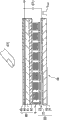
As shown in Figure 4, display device 1 comprises: pixel substrate 2, relative substrate 4 and liquid crystal layer 6.Substrate 4 is staggered relatively with pixel substrate 2 relatively, and liquid crystal layer 6 is inserted between pixel substrate 2 and the relative substrate 4.
Substrate 4 comprises substrate of glass 41, color filter (color filter) 42 and public electrode 43 relatively.Color filter 42 is formed on the surface of substrate of glass 41, and public electrode 43 is formed on the color filter 42.Color filter 42 is by red (R) of for example periodic arrangement, green (G) and blue (B) three colour filters configurations, and each of one group of R, G and B three looks and display pixel (pixel electrode 22) is interrelated.Public electrode 43 also is used as the sensor drive electrode, and this sensor is responsible for touching the part of the touch sensor that detects operation with the drive electrode configuration, and public electrode 43 is corresponding with the drive electrode E1 among Figure 1A.
The reverse side of substrate of glass 41 has formed sensor detecting electrode (touch detecting electrode) 44, and uses on the detecting electrode 44 at this sensor, and polarizing plate 45 is provided.This sensor has configured the part of touch sensor with detecting electrode 44, and corresponding with the detecting electrode E2 of Figure 1A.
Note, providing alignment film (alignment film) between liquid crystal layer 6 and the pixel substrate 2 and between liquid crystal layer 6 and relative substrate 4.Lower surface one side of pixel substrate 2 is provided with light light incident side (light-incident-side) polarizing plate, but not shown in figures.
[public electrode 43 and the sensor exemplary detailed configuration of detecting electrode 44]
Fig. 5 is provided for the public electrode 43 of relative substrate 4 and the skeleton view that sensor is used detecting electrode 44, shows its exemplary configuration.In the example of Fig. 5, public electrode 43 is divided into the electrode pattern of a plurality of shape of stripes, and each electrode pattern is laterally extending in the accompanying drawings.This electrode pattern is illustrated as " n " bar (wherein " n " is the integer more than or equal to 2) public electrode 431 to 43n.Electrode pattern is sequentially provided the common drive signal Vcom of common electrode drive device 43D, and is then driven be used to lining by line scan with the time division way of describing after a while.On the other hand, by the configuration of the electrode pattern of a plurality of shape of stripes, the electrode pattern of this shape of stripes extends in the direction vertical with the bearing of trend of the electrode pattern of public electrode 43 sensor with detecting electrode 44.Sensor each output detection signal Vdet of electrode pattern of detecting electrode 44, and for example, the detection signal Vdet that obtains is imported into such as Fig. 6 to testing circuit 8 shown in Figure 8.
[exemplary configuration of exemplary pixel configuration and driver]
Each is the exemplary configuration that the driver of exemplary pixel configuration in the display device 1 and a plurality of types wherein is shown for Fig. 6 and Fig. 7.In display device 1, in effective display area territory 100, a plurality of pixels (display pixel 20) are arranged with matrix.Each is comprised of the pixel here TFT elements T r and liquid crystal cell LC.
In the example of Fig. 6, display pixel 20 is connected respectively to gate line 126, signal wire (source electrode line) 25 and public electrode 431 to 43n.At this, gate line 126 is connected to gate drivers 26D, and signal wire 25 is connected to unshowned source electrode driver, and public electrode 431 to 43n is connected to common electrode drive device 43D.As mentioned above, common electrode drive device 43D be operated with provide in order respectively common drive signal Vcom (Vcom (1) to Vcom (n)) to public electrode 431 to 43n.This common electrode drive device 43D for example comprises, shift register 43D1, COM selection part 43D2, level shifter (level shifter) 43D3 and COM impact damper 43D4.
Shift register 43D1 is the logical circuit of the sequential transfer (sequential transfer) for input pulse.More specifically, this shift register 43D1 has been provided transfer trigger pulse (transfertrigger pulse) (initial pulse), shifts so that responsively begin clock.When repeatedly carrying out the input of initial pulse an image duration, the time transfer repeats each input.At this, shift register 43D1 can be configured to a plurality of transfer logic circuits, is used for controlling respectively a plurality of public electrode 431 to 43n.If should configure, then control circuit can increase size, and therefore, the gate drivers as shown in Figure 7 that the transfer logic circuits that obtains can preferably be applicable to describe after a while and the shared use of common electrode drive device, more preferably, the transfer logic circuits that obtains can be provided separately and do not considered the number of public electrode 43.
Whether COM selects part 43D2 is to the logical circuit of each output common drive signal Vcom of the display pixel 20 in effective display area territory 100 for control.Be that COM selects part 43D2 to be responsible for controlling according to each position of the display pixel 20 in the effective display area territory 100 output of common drive signal Vom.Although provide after a while detailed illustrating, for example, if COM selects part 43D2 to be provided available gating pulse, then the outgoing position of common drive signal Vcom can be based on horizontal line or through changing arbitrarily behind a plurality of horizontal cycles.
Level shifter 43D3 will select the potential shift of the common drive signal Vcom of part 43D2 to arrive the circuit that enough is used for the level of control from COM.
COM impact damper 43D4 be for order provide common drive signal Vcom (Vcom (1) is to Vcom (n)) last-output logic circuit, and comprise for example output buffer circuit or on-off circuit.
On the other hand, in the example of Fig. 7, display pixel 20 is connected source electrode line with gate line 126, public electrode 431 to 43n respectively with signal wire) 25 be connected.At this, gate line 126 and public electrode 431 to 43n all are connected to grid/common electrode drive device 40D, and signal wire 25 is connected to unshowned source electrode driver.Grid/common electrode drive device 40D is operated to pass through corresponding gate line 126 and provides gate drive signal to each of display pixel 20, and sequentially provides common drive signal Vcom (Vcom (1) is to Vcom (n)) to public electrode 431 to 43n respectively.This grid/common electrode drive device 40D for example comprises shift register 40D1, enables/control section 40D2, grid/COM selects part 40D3, level shifter 40D4 and grid/COM impact damper 40D5.
Shift register 40D1 has the function of the shift register 43D1 that is similar to foregoing description, except it is shared by gate drivers and common electrode drive device.
Enable/control section 40D2 is used for catching enabling pulse by the time clock of using shift register 40D1 to shift, produces the pulse of control gate polar curve 126.
Grid/COM selects part 40D3 whether to control each output common drive signal Vcom of the display pixel 20 in the effective display area territory 100 and the logical circuit of signal VG.That is, grid/COM selects part 40D3 to be responsible for position according to each of the display pixel 20 in the effective display area territory 100 for example, controls the output of common drive signal Vcom and the output of signal VG.
Level shifter 40D4 is the circuit that will select the potential shift of the electromotive force of common drive signal Vcom of part 40D3 and signal VG to the level that enough is used for controlling from grid/COM.
Grid/COM impact damper 40D5 be for order provide common drive signal Vcom (Vcom (1) is to Vcom (n)) and signal VG (VG (1) is to VG (n)) at last-output logic circuit, and comprise for example output buffer circuit or on-off circuit.
Note, in the example of Fig. 7, display device 1 is provided with the T/GDC/DC converter 20D except the assembly of foregoing description.This T/GDC/DC converter 20D is as T/G (timing generator) and DC/DC (DC-DC) converter.
[comprising the demonstrative circuit configuration of source driving signal S and testing circuit 8]
Fig. 8 shows the source driving signal S that comprises Figure 1B and is used for touching the testing circuit 8 that detects operation, and the demonstrative circuit configuration that is used as the timing controlled part 9 of timing generator.In the figure, capacitor element C11 to C1n is with the corresponding capacitor element of (static) capacitor element of the Fig. 5 that forms between the detecting electrode 44 with public electrode 431 to 43n and sensor.
Source driving signal S is provided for each of capacitor element C11 to c1n.Each comprises SW control section 11, two on-off elements 12 and 15, two inverter circuits (logic " non-") 131 and 132 and operational amplifier 14 this source driving signal S.SW control section 11 is used for the on/off state of gauge tap element 12, thus the connection between control power supply+V and inverter circuit 131 and 132.The input end of inverter circuit 131 is connected to an end of on-off element 12, the i.e. end relative with power supply+V, and is connected to the output terminal of inverter circuit 132.The output terminal of inverter circuit 131 is connected to the input end of inverter circuit 132, and is connected to the input end of operational amplifier 14.By this configuration, this inverter circuit 131 and 132 each pierce circuit (oscillator circuit) as output predetermined pulse signal.Operational amplifier 14 is connected to two power supplys, namely+V and-V.On-off element 15 is controlled as the on/off state according to the timing controling signal CTL1 from timing controlled part 9.More specifically, this on-off element 15 is set up each one distolateral (each side of public electrode 431 to 43n) of capacitor element C11 to C1n to the connection of the output end (mains side of common drive signal Vcom) of operational amplifier 14, perhaps sets up its grounding connection.So, source driving signal S provides common drive signal Vcom to each capacitor element C11 to C1n.
Testing circuit 8 (voltage-level detector DET) comprises the resistor R of amplifier section 81, A/D (analog/digital) converter part 83, signal processing 84, frame memory 86, coordinate Extraction parts 85 and foregoing description.In this testing circuit 8, it is distolateral that input end Tin is connected to the residue of all capacitor element C11 to C16, and namely sensor is with detecting electrode 44 sides.
Resistor R is disposed between the tie point P and ground of the operational amplifier 811 on positive input terminal (+) side.Resistance R is provided for that sensor is not in quick condition with detecting electrode 44 but keeps stable.Therefore, in testing circuit 8, make the value of detection signal Vdet avoid fluctuation and change.In addition can be by the advantage of this resistor R release electrostatic to ground.
A/D converter part 83 is be used to the amplification that utilizes amplifier section 81 analog detection signal Vdet to be converted to numeral, and comprises unshowned comparer.This comparer is used for detection signal and the predetermined threshold voltage Vth (with reference to part (A) and the part (B) of figure 3) of relatively input.Note, for the A/D conversion in A/D converter part 83 so, sampling timing is controlled by the timing controling signal CTL2 from timing controlled part 9.
To the digital detection signal that obtains that is provided by A/D converter part 83, signal processing 84 applies predetermined signal processing, and for example the numeral of noise is eliminated, or frequency information is converted into positional information.Although details is described after a while, signal processing 84 is so configured in order to carry out predetermined computation, be used for to eliminate any impact of the noise (internal noise) that (minimizing) caused by write operation of picture signal.The frame memory 86 of the table of corrections of describing after a while with storage etc. is carried out this calculating.
Coordinate Extraction parts 85 is used for finding testing result, and what namely the user touched has or nothing, if having, finds the coordinate of position, and from output terminal Tout Output rusults.For this operation, the detection signal that coordinate Extraction parts 85 uses detection signals, namely finish from the elimination of passing through above-mentioned internal noise of signal processing 84 is as the basis.
It is upper as peripheral IC (integrated circuit) that this testing circuit 8 can be installed in FPC (flexible print circuit), perhaps is installed in the substrate.Perhaps, testing circuit 8 can be formed near the relative substrate 4 the zone, namely press in the territory at non-display area or frame (frame), or near the zone pixel substrate 2.At this, from the integrated viewpoint of simplifying by circuit, think to form testing circuits 8 more preferably in pixel substrate 2, namely each circuit of the demonstration control usefulness by original formation in pixel substrate 2 is realized integrated.For this configuration, testing circuit 8 in the pixel substrate 2 can use the contact conductive pole (unshowned) that is similar to contact conductive pole 7 to be connected to the electrode pattern that sensor is used detecting electrode 44, and can provide detection signal Vdet to testing circuit 8 with detecting electrode 44 from sensor.
[advantage of display device 1 and effect]
Next advantage and the effect of the display device 1 of the first embodiment are described.
[1. basic operation]
In display device 1, the display driver of pixel substrate 2, for example common electrode drive device 43D provides common drive signal Vcom line by line to the electrode pattern (public electrode 431 is to 43n) of public electrode 43.Display driver also provides picture element signal (picture signal) by source electrode line 25 to each of pixel electrode 22, and synchronously controls line by line the switch of the TFT (TFT elements T r) of pixel electrode by gate line 126 with it.Therefore, apply electric field based on display pixel to liquid crystal layer 6, so that this layer is modulated to mesomorphic state (liquid crystalline state).Electric field herein in vertical direction, namely on perpendicular to the direction of substrate by common drive signal Vcom and picture signal definition.In this way, finish demonstration by so-called anti-phase driving (inversion driving).
On the other hand, in relative substrate 4 sides, capacitor element C1 (capacitor element c11 to C1n) is formed on the electrode pattern of public electrode 43 and each cross section between the sensor usefulness electrode pattern of electrode 44.Herein, such as the arrow of Fig. 5, be shown in the arrow of direction of scanning, if apply in order common drive signal Vcom with time division way to the electrode pattern of public electrode 43, following situation occurs.That is, by applying of this signal, be formed on the electrode pattern of public electrode 43 and sensor and be recharged/discharge with the capacitor element C11 to C1n of delegation of the cross section between the electrode pattern of electrode 44.As a result, sensor each output size of electrode pattern detection signal Vdet corresponding with the value of capacitor element C1 of electrode 44.When user's finger was not just contacting relative substrate 4 surperficial, detection signal Vdet size almost was constant.When the scanning that utilizes common drive signal Vcom continues, moved line by line as this row capacitor element C1 of the target of charge/discharge.
At this, extremely part (C) is by the line by line driving of the electrode pattern of the exemplary so public electrode 43 that illustrates for the part (A) such as Fig. 9, and one group of (that is, one) electrode pattern of public electrode 43 is preferably through driving line by line.More specifically, the drive wire L as one group of electrode pattern comprises position-detection drive wire L1 and display driver line L2.Position-detection drive wire L comprises the multirow electrode pattern, and display driver line L2 comprises minority row (being delegation in this example) electrode pattern.This configuration advantage ground reduces any possible deterioration to pattern quality that is caused by the row corresponding with the shape of the electrode pattern of public electrode 43, point etc.
When user's finger touch arrived lip-deep any position of relative substrate 4, the original any capacitor element C1 that is formed into the part of touch had been added capacitor element C2 by finger.The result, when the part of this touch of scanning, that is, when any electrode pattern of the public electrode 43 corresponding with the part that touches had been applied in common drive signal Vcom, the value of detection signal Vdet was less than the detection signal Vdet of the lip-deep remainder that is used for relative substrate 4.So testing circuit 8 (Fig. 8) compares this detection signal Vdet and threshold voltage vt h, and when determining detection signal Vdet less than threshold voltage vt h, testing circuit 8 determines that these parts are the part of touch.The part that applies regularly and regularly identify less than the detection of the detection signal Vdet of threshold voltage vt h touch by common drive signal Vcom.
So, providing of the present embodiment in the display device 1 of touch sensor, the original public electrode 43 that offers liquid crystal display cells also is used as one of pair of electrodes that touch sensor uses, this pair of electrodes is a pair of of drive electrode and detecting electrode.And in the display device 1 of the present embodiment, also be used as touch-sensor actuation signal as the common drive signal Vcom of display drive signals.Use this configuration, the capacitive touch sensor that obtains only needs newly to comprise sensor detecting electrode 44, and does not need newly to provide touch sensor to drive signal.This configuration has advantageously been simplified like this.
And, in the display device that touch sensor is provided formerly (the open No.2008-9750 of Japanese unexamined patent), flow to the electric current of sensor with the pin-point accuracy measurement, and find the part of touch by analog computation with the measured value that obtains as the basis.On the other hand, in the display device 1 of the first embodiment, only need digitally to detect any relevant variation (variation of electromotive force) in electric current that is with or without user's touch, so that can increase accuracy in detection by the testing circuit of easy configuration.And in display device 1 of the present invention, the public electrode 43 that applies common drive signal Vcom and the sensor that recently provides are provided form capacitor between with detecting electrode 44 original, and by any variation of the capacitor that caused by user's finger touch, carry out to touch and detect.The display device that obtains can also be applicable to wherein user's usually unsettled mobile unit use of electromotive force.
In addition, in the display device 1 of the present embodiment, sensor has been divided into a plurality of electrode patterns with detecting electrode 44, and the electrode pattern of dividing like this drives separately with time division way, also enables thus the detection of the part that touches.
[the advantage of the feature of 2. inventing; Use the detection operation of noise Processing for removing]
Next, by with reference to figures 10 to Figure 18 G, describe in detail about using the detection operation of noise Processing for removing, using the detection operation of noise Processing for removing is one of feature of the present invention.
At first, shown in the part (A) of Figure 10, when showing at the image as the part (B) of Figure 10 and part (C) that control period, common drive signal Vcom are synchronized with drive cycle (1H period) and during reversal of poles, the detection waveform of detection signal Vdet looks the part (D) that look like Figure 10 and the detection waveform of (F) partly.That is, be synchronized with this reversal of poles and reversal of poles occurs, similarly, after reversal of poles so, owing to flowing to the leakage current of above-mentioned resistor R, signal value is decayed gradually.
For example, in the picture element signal that writes (picture signal) during writing with black of writing such as the white shown in the part (B) of Figure 10 and part (C), the detection waveform of detection signal Vdet comprises the part (E) that derives from such as Figure 10 and the noise that writes shown in (F) partly.For specifically, what the 1H period comprised that do not apply picture signal non-write period Δ tA and the picture signal of applying arranged writes period Δ tB.In writing period Δ tB, detection waveform shows the fluctuation according to the gray level of picture signal.According to this time point, the i.e. gray level of the picture signal after reversal of poles, the detection waveform of detection signal Vdet is included in the noise (internal noise) that the picture signal after the reversal of poles causes, such as the part (E) of Figure 10 with partly shown in the arrow of (F).Particularly, this detection waveform is included in black during writing and common drive signal Vcom homophase and the noise after this reversal of poles anti-phase with it of white during writing.So, in writing period Δ tB, internal noise changes the detection waveform of detection signal Vdet according to the gray level of picture signal, cause thus being difficult to distinguish the different variations in detection waveform (part of Fig. 3 (A) and part (B)) that cause by the touch (near for example outside object) that is with or without object.
For example, as shown in figure 11, followed non-writing among the period Δ tA after the reversal of poles of common drive signal Vcom, with writing period Δ tB relatively, the variation of amount that is touched the voltage that causes by object is very large.Therefore, for example, considered the high sensitivity of the detection that any object touches, moment before the picture signal that is inverted for polarity begins write operation preferably, namely write the detection of period Δ tA after carrying out reversal of poles and operate non-.
In view of this, in the first embodiment, shown in exemplary at Figure 12 to Figure 17, the element in testing circuit 8, be to carry out in signal processing 84, frame memory 86 and the coordinate Extraction parts 85 to have this object detection that internal noise is eliminated.Particularly, in signal processing 84 and frame memory 86, come correct detection signal Vdet according to the gray level of the picture signal when obtaining detection signal Vdet.More specifically, using noise data (is the reference noise data; With reference to Figure 14 A and Figure 14 B that describe after a while) and picture signal come correct detection signal Vdet.In noise data, the value of the detection signal of the noise (internal noise) that the gray level of picture signal and the write operation that comprises by picture signal cause is relevant.In coordinate Extraction parts 85, eliminate (minimizing) detection signal afterwards at this internal noise and be used to carry out the detection operation.Similarly, describe after a while, can carry out and detect operation, eliminate simultaneously (minimizings) causes the noise (internal noise) that produces in detection signal Vdet owing to the write operation in the picture signal of image demonstration control period any possible impact.Note, for the elimination of this internal noise, have technology 1 and the technology 2 for example described after a while.
[2-1. technology 1]
Figure 12 is for the exemplary method of internal noise elimination, is the process flow diagram of technology 1.Utilize technology 1, use the predetermined correction table (describing after a while) that is stored in the frame memory 86 to come correct detection signal Vdet.
At first, signal processing 84 and frame memory 86 obtain this picture signal (step S11) shown in the part (A) such as Figure 13 when obtaining detection signal Vdet.Below, described is the exemplary case of the black and white crenellation pattern of the picture signal in the part (A) of utilizing Figure 13.
Next, signal processing 84 usefulness are carried out predetermined computation (step S12) in the picture signal that step S11 obtains with the experimental data corresponding with above-mentioned noise data.This experimental data is to shift to an earlier date ready experimental data, for example data of Figure 14 A and Figure 14 B by predetermined experiment.Namely, in noise data, signal wire 25 to write voltage (gray level of picture signal) relevant with the value of detection signal Vdet, wherein, this detection signal Vdet comprises by the internal noise that shows that at image the write operation of control period by the picture signal of gray level causes.Using the reason of the noise data that is configured by experimental data is to test to estimate by the quantification of internal noise the amount of internal noise, because touch sensor comprises various types of capacitor assemblies.Such as the experimental data of Figure 14 A and Figure 14 B, when the amplitude of the amplitude of detection signal Vdet and common drive signal Vcom was anti-phase, if detection signal Vdet comprises any internal noise, its amplitude became less.On the other hand, when this amplitude same phase time in a large amount of images, the amplitude of detection signal Vdet becomes larger.That is, utilize the experimental data of Figure 14 A and Figure 14 B, the voltage that writes of signal wire 25 is set up simple linear formula with the value of the detection signal Vdet that comprises internal noise.So, the gray level of the picture signal that use to obtain is as the basis, can easily obtain comprising the value of the detection signal Vdet of internal noise.
Next, use obtains in step S12 is used for comprising the value of detection signal Vdet of the internal noise of experimental data, and signal processing 84 and frame memory 86 are prepared the value (step S13) of the detection signal in above-mentioned table of corrections according to the gray level of picture signal.Particularly, shown in the part (B) of Figure 13, based on the intended pixel zone that comprises a plurality of image pixels 20, prepared the table of corrections that storage is used for the value that the detection signal Vdet to the internal noise that comprises experimental data detects.Herein, the intended pixel zone for example is the single-bit correction zone 200 among Figure 15 A and Figure 15 B.This single-bit correction zone 200 comprises respectively the electrode pattern of sensor detecting electrode 44 at the center of the length (center distance Pa) that is positioned on the horizontal line direction.In addition, each width (drive wire width (width of position-detection drive wire L1) Wb) of the electrode pattern of public electrode 43 is set to the length in the single-bit correction zone 200 on the perpendicular line direction.That is, in this single-bit correction zone 200, the length on the horizontal direction is transducer spacing Pa, and the length on the direction of perpendicular line is drive wire width W b.Table of corrections is for each single-bit correction zone 200, and based on the average gray level of the picture signal that is used to all display pixels 20 in the single-bit correction zone 200, storage comprises the value of the detection signal Vdet of internal noise.Note, in the example of Figure 15 A, show that IC 91D provides with touch-sensor IC 92D separates, and the wiring pattern of these IC by FPC90 couples mutually.On the other hand, in the example of Figure 15 B, the demonstration that provides/touch sensor IC 93D shows that wherein IC and touch sensor IC are integrated on the chip.Herein, the above-mentioned picture signal when obtaining detection signal Vdet is provided to touch-sensor IC (Figure 15 A) by FPC 90 from demonstration IC indirectly, perhaps directly provides (Figure 15 B) by the wiring pattern in the IC.
Next, this detection signal Vdet that signal processing 84 and frame memory 86 obtain shown in the part (C) of Figure 13, the detection signal Vdet (step S14) that is namely detected with detecting electrode 44 by sensor.
Next, use the table of corrections of preparing among the step S13, therefore the detection signal Vdet that obtains among signal processing 84 and the frame memory 86 aligning step S14 produces correction signal (step S15).More specifically, as the part (D) of Figure 13 exemplarily shown in, for each of above-mentioned single-bit correction zone 200, signal processing 84 and frame memory 86 carried out subtracting each other of two signal values or is divided by (this example is for being divided by), and these two signal values namely are included in the value of the detection signal Vdet of the value of detection signal Vdet of the internal noise in the table of corrections and acquisition.This has correspondingly proofreaied and correct the detection signal Vdet that obtains, so that produced correction signal.At this moment, signal processing 84 and frame memory 86 preferably utilize the correction result in all single-bit correction zones 200 on the horizontal line direction, and again proofread and correct the detection signal Vdet that obtains for each the single-bit correction zone 200 on horizontal line.Such as after a while described (Figure 18 A to Figure 18 G), this has advantageously reduced the impact that is included in the internal noise among the detection signal Vdet more, so that accuracy in detection can be added to higher degree.
Next, the correction signal that produces among 86 couples of step S15 of signal processor 84 and frame memory is carried out threshold calculations (binarization), therefore produces the binary data (step S16) such as the part (E) of Figure 13.
Then, coordinate Extraction parts 85 is by so elimination of internal noise (minimizing), detection signal (binary data) is carried out mark process (labeling process) (step S17), then carry out by the extracting position coordinate and detect operation (step 18).Detection EO in the technology 1 among Figure 12.
Utilize so technology 1, come correct detection signal Vdet with the predetermined correction table that is stored in the frame memory 86.This has enabled to eliminate (minimizing) the detection operation that produces any impact of noise (internal noise) owing to showing the write operation of control period picture signal at image in detection signal Vdet.
[2-2. technology 2]
Figure 16 is for another exemplary method of internal noise elimination, is the process flow diagram of technology 2.Utilize this technology 2, be different from above-mentioned technology 1, do not come correct detection signal Vdet with above-mentioned table of corrections.That is, by following between detection period picture signal and the predetermined computation between the detection signal Vdet, do not use the direct correct detection signal of this table of corrections Vdet.
At first, be similar to the step S11 in the technology 1, the picture signal that signal processing 84 obtains such as the part (A) of Figure 17, i.e. picture signal (step S21) when obtaining detection signal Vdet.And in this example, described is the exemplary case of the black and white crenellation pattern of the picture signal in the part (A) of utilizing Figure 17.
Next, be similar to the step S14 in the technology 1, signal processing 84 obtains by this detection signal Vdet (step 22) of sensor with the part such as Figure 17 (B) of detecting electrode 44 detections.
Next, signal processing 84 use the picture signal that obtains among the step S21 and comprise shown in Figure 14 A and Figure 14 B as described in the value of detection signal Vdet of internal noise in the experimental data, proofread and correct the detection signal Vdet (step S23) that in step S22, obtains.Particularly, for the correction such as so detection signal Vdet of the part (C) of Figure 17, by using the value of the detection signal Vdet that comprise internal noise corresponding with the gray level of picture signal, to each of single-bit correction zone 200, the value of the detection signal Vdet of normalization acquisition.After this is proofreaied and correct, produce the correction signal for detection of signal Vdet.At this moment, be similar to technology 1, signal processing 84 is preferably utilized the correction result in all the single-bit correction zones 200 on the horizontal line direction, and again proofreaies and correct the detection signal Vdet of the acquisition in each the single-bit correction zone 200 in horizontal line.
Next, the correction signal that produces among 84 couples of step S24 of signal processor is carried out threshold calculations (binarization), therefore produces the binary data (step S24) such as the part (D) of Figure 17.
Then, 85 pairs of internal noises of coordinate Extraction parts are eliminated (minimizing) detection signal (binary data) afterwards and are carried out mark processing (step S25), then carry out by the extracting position coordinate and detect operation (step 26).Detection EO with the technology 2 of Figure 16.
So, utilize technology 2, by the predetermined computation between the picture signal between detection period and detection signal Vdet, do not use table of corrections, directly correct detection signal Vdet.This produces the advantage that does not need to comprise table of corrections the advantage that obtains except operation technique 1.
In above-mentioned the first embodiment, based on the detection signal Vdet that is obtained in response to any variation in the capacitor by the touch detecting electrode, the position that detected object touches.And testing circuit 8 so is configured to carry out and detect operation by coming correct detection signal Vdet based on the gray level of the picture signal when obtaining detection signal Vdet.By this configuration, no longer need to use screen layer, and can carry out the impact that detects operation and reduce (elimination) internal noise.So, in the display device that has been provided the capacitive touch sensor that obtains, do not use screen layer, can increase the accuracy of object detection yet.
Figure 18 G shows the exemplary effect of the internal noise elimination of method in a plurality of exemplary image signal patterns (Figure 18 A to Figure 18 F) of the internal noise elimination that utilizes the present embodiment.In Figure 18 G, term " unit area correction " expression is to the result of the correction of each execution in single-bit correction zone 200.Correction result in term " horizontal zone correction " expression utilization all single-bit correction zones 200 on horizontal line comes the result to the correction of each execution in the single-bit correction zone 200 on horizontal line.In Figure 18 G, the situation that " * " expression does not wherein have the completing place to detect owing to a large amount of internal noises among the detection signal Vdet.And in Figure 18 G, " △ " though the situation that expression wherein has a small amount of internal noise also can the completing place to detect in detection signal Vdet, and " zero " expression wherein can the completing place detects and without any the situation of internal noise problem.Show such as the testing result among Figure 18 G, in the row of " without proofreading and correct ", the picture signal pattern of Figure 18 A illustrates " zero ", and remaining picture signal pattern all is shown " * ".In the row of " unit area correction ", the picture signal pattern of Figure 18 E and Figure 18 F illustrates " △ ", and the picture signal pattern of remaining A to D all is shown " zero ".This result shows the minimizing along with internal noise, and the accuracy of position probing increases.In addition, in the row of " horizontal zone correction ", all picture signal patterns of Figure 18 A to 18F all are shown " zero ", comprise Figure 18 E and Figure 18 F.So, when carrying out " horizontal zone corrections ", internal noise can be reduced also lowlyer than the internal noise when the execution " unit area correction ", and the accuracy of position probing increase in addition higher.
[example of the modification of the first embodiment]
Described in above-mentioned the first embodiment is that above-mentioned noise data is the example that shifts to an earlier date ready experimental data by predetermined experiment, and the example of following modification also is kind of a possibility.In the example of modification below, the internal noise detection signal based on use detecting electrode 44 from sensor by supply predetermined detection pattern signal produces noise data.This check pattern signal is the check pattern signal that obtains from display control circuit (unshowned source electrode driver) in the blanking period of describing after a while.
Particularly, in the example of this modification, in the element in testing circuit 8, namely in signal processing 84, frame memory 86 and coordinate Extraction parts 85, calculate the internal noise amount according to the gray level of picture signal, shown in Figure 19 to Figure 21 is exemplary.More specifically, in signal processing 84 and frame memory 86, obtain internal noise detection signal from sensor with detecting electrode 44 in the blanking period.This blanking period and is vertical (V) blanking period Tvb or level (H) blanking period Thb between each effective display time interval T1.As describing after a while, by by unshowned source electrode driver supply predetermined detection pattern signal (picture signal by predetermined gray level of describing after a while), obtain this internal noise detection signal from sensor with detecting electrode 44.
Figure 19 is the process flow diagram of the exemplary method that is used for internal noise calculating in the example of this modification.Each shows timing waveform figure for the exemplary method of calculating in vertical (V) the blanking period or at the internal noise of level (H) blanking period Figure 20 and Figure 21.In Figure 20 and Figure 21, (A) expression horizontal-drive signal Hsync, (B) expression horizontal-drive signal Hsync, (C) presentation video signal data, (D) expression common drive signal Vcom.And in Figure 20 and Figure 21, (E), (G) and (I) each check pattern signal that is illustrated in the V blanking period or in the H blanking period, is used for being supplied to signal wire (source electrode line) 25, namely, " Sig DC " expression is in the DC signal of fixed potential, " SigBlack " expression black write signal, and " Sig White " represents white write signal.And in Figure 20 and Figure 21, (F), (H) and (I) respectively expression as the result's of supply " Sig DC ", " Sig Black " and " Sig White " detection signal Vdet (noise detecting signal).
At first, signal processing 84 and frame memory 86 obtain predetermined reference data (S31 of Figure 19).For example, this reference data is in the DC signal of fixed potential, i.e. condition when " Sig DC " and the detection signal Vdet that obtains about utilizing when use.This condition herein comprises and does not have touch or deposit nigh non-detected object, and do not have the external noise that is caused by external environment condition.
Next, signal processing 84 and frame memory 86 in the blanking period, be among V blanking period Tvb or the H blanking period Thb, obtain from the internal noise detection signal (step S32) of sensor with detecting electrode 44.More specifically, in this example, in a plurality of blanking period, from a plurality of each check pattern signal, be that the picture signal of the gray level of the signal of fixed potential and variation obtains internal noise detection signal (step S321 is to step S324).
More specifically, at first in the blanking period, when the DC of fixed potential signal " Sig DC " when being applied to source electrode line 25, because signal wire does not change on electromotive force, this is the main cause of internal noise, therefore, can eliminate the impact of internal noise.Therefore, the detection waveform that obtains (" signal A ") that obtains with detecting electrode 44 from sensor can avoid the impact (step S321 and S324, (E) among Figure 20 and Figure 21 and (F)) of internal noise.
On the other hand, when when the blanking period has applied black write signal (black signal) " Sig Black " to source electrode line 25, except the waveform of the detection signal Vdet that is not subjected in the impact on the source electrode line 25, can also obtain the internal noise amount corresponding with the demonstration of this black signal.That is, from sensor with the detection waveform (" signal B ") of the detecting electrode 44 provides internal noise detection signal corresponding with this gray level (step S322 and S324, (G) among Figure 20 and Figure 21 and (H)).
Similarly, when in the blanking period, source electrode line 25 being applied white write signal (white image signal) " Sig White ", except the waveform of the detection signal Vdet that is not subjected in the impact on the source electrode line 25, can also obtain the internal noise amount corresponding with the demonstration of this white image signal.That is, from sensor with the detection waveform (" signal C ") of the detecting electrode 44 provides internal noise detection signal corresponding with this gray level (step S323 and S324, (I) among Figure 20 and Figure 21 and (J)).
So, in step S32, can identify the waveform of internal noise detection signal, namely not have the waveform " signal A " of internal noise impact, at the waveform that has internal noise during the black display " signal B " with during white displays, have the waveform " signal C " of internal noise.The waveform of the identification that obtains can be used in the following calculating.
Next, signal processing 84 and frame memory 86 are based on the detection waveform that obtains in step S32, namely in the present example " signal A " be to " signal C ", carry out predetermined computation (poor calculating) (step S33), calculate thus internal noise amount (step S34).The processing that the internal noise of Figure 19 calculates finishes.
So, in the example of this modification, based on by in the blanking period, use the internal noise signal of detecting electrode 44 acquisitions from sensor from display control circuit supply predetermined detection pattern, set up noise data.Therefore, contrast with above-mentioned the first embodiment, more suitably the amount that obtains of (in the better moment) acquisition internal noise.
[2. the second embodiment]
What the following describes is the second embodiment of the present invention.Be different from the first embodiment, in a second embodiment, display element is illustrated at the liquid crystal cell in the lateral electric field mode (lateral electric field mode).
[exemplary configuration of display device 1B]
Figure 22 is providing of the present embodiment the has been shown figure of section configuration of major part of display device 1B of touch sensor.Each is illustrated in the detailed configuration of the pixel substrate (the pixel substrate 2B that describes after a while) among this display device 1B Figure 23 A and Figure 23 B.More specifically, Figure 23 A illustrates the section configuration of display device 1B, and Figure 23 B shows this configuration in the planimetric map mode.Each is the skeleton view of display device 1B for Figure 24 A and Figure 24 B, shows its configuration.Note, in these accompanying drawings, be provided identical Reference numeral as identical any element among Fig. 4 in above-mentioned the first embodiment etc., and if end suitably then no longer.
Relatively substrate 4B is by substrate of glass 41 and color filter 42 configurations that form in the one side of substrate of glass 41.The another side of substrate of glass 41 is comprised of with detecting electrode 44 sensor, and uses on the detecting electrode 44 at sensor, and polarizing plate 45 is provided.This sensor configures the part of touch sensors with detecting electrode 44, and corresponding with the detecting electrode E2 of Figure 1A.As shown in Figure 5, sensor is divided into a plurality of electrode patterns with detecting electrode 44.Sensor can be processed by film with detecting electrode 44 and directly be provided on the relative substrate 4B, perhaps can indirectly be provided.If this situation, touch detecting electrode 44 and can be formed on the unshowned film substrate, and with touch the film substrate that obtains that detecting electrode 44 forms thereon together and can be attached on the surface of relative substrate 4B.This film substrate that obtains can not only be attached between glass and the polarizing plate, also can be attached at the upper surface of polarizing plate, perhaps can generate in the film of configuration polarizing plate.
By with reference to figure 24A and 24B, provide more detailed description.In the liquid crystal cell of FFS pattern in the present example, the public electrode 43 that forms at pixel substrate 2B has been provided the pixel electrode 22 via insulation course 23 thereon.Pixel electrode 22 is pixel electrodes of moulding such as broach, and so forms orientation mould 26 to cover pixel electrode 22.Between the side of substrate 4B provides relatively alignment film (alignment film) 26 and another alignment film 46, sandwich liquid crystal layer 6.Two polarizing plates 24 and 45 are disposed in the cross prisms (crossed nicol).Two alignment films 24 are identical with arbitrary light transmission shaft (light-transmission axis) of polarizing plate 24 or 25 with 46 frictional direction (rubbing direction).Figure 24 A and model shown in Figure 24 B be wherein frictional direction with in the identical situation of the light transmission shaft of the polarizing plate 45 of light exit (light-exit) side.And in the present example, the direction of two alignment films 26 and 46 frictional direction and the light transmission shaft of polarizing plate 45 all is set in the scope of the direction that is used for defining the liquid crystal molecule rotation, almost parallel with the bearing of trend (longitudinal direction of broach) of pixel electrode 22.
[advantage of display device 1B and effect]
What the following describes is advantage and the effect of the display device 1B of the second embodiment.
By reference 24A to 25B, what at first describe is the principle of the display operation of FFS mode liquid crystal element.Each is the cross section view of amplification that the major part of liquid crystal cell is shown for Figure 25 A and 25B.Particularly, Figure 25 A shows the state of the liquid crystal cell when not applying electric field; Figure 25 B shows the state of the liquid crystal cell when having applied electric field.
Do not applying voltage (Figure 24 A and Figure 25 A) in the situation between public electrode 43 and the pixel electrode 22, each axle of the liquid crystal molecule 61 of configuration liquid crystal layer 6 is vertical with the light transmission shaft of the polarizing plate 24 of light incident side, and parallel with the light transmission shaft of the polarizing plate 45 of light exit side.By this configuration, the incident light " h " that passes the polarizing plate 24 of light incident side arrives the polarizing plate 45 of light exit side, and does not cause the phase difference in the liquid crystal layer 6, and is absorbed in order to show at this and is black.On the other hand, by between public electrode 43 and pixel electrode 22, applying voltage (Figure 24 B and Figure 25 B), by the alignment direction of the transverse electric field E rotation liquid crystal molecule 61 that produces between the pixel electrode in order to tilt with respect to the bearing of trend of pixel electrode 22.At this moment, the electric field intensity during the white displays optimised so that on thickness direction at about 45 degree of liquid crystal molecule 61 rotation at liquid crystal layer 6 centers.As a result, the incident light " h " that passes the polarizing plate 24 of light incident side causes phase difference when passing liquid crystal layer 6, therefore by linear polarization (linearly polarized) 90 degree rotations.The light that obtains passes light exit side polarizing plate 45, so that the demonstration that obtains will be white in color.
Next describedly be the demonstration control operation among the display device 1B and touch detect operation.These class of operation are similar to the operation among the first embodiment of foregoing description, if suitably then no longer describe.
The display driver (not shown) of pixel substrate 2B is supplied common drive signal Vcom line by line to the electrode pattern of public electrode 43.Display driver also passes through source electrode line 25 to pixel electrode 22 supply image signals, and with it synchronously, by gate line 126, controls line by line the switch of the TFT of pixel electrode.As a result, to each pixel, apply electric field to liquid crystal layer 6, so that regulate this layer according to mesomorphic state.Electric field herein in the horizontal, namely on the direction parallel with substrate by common drive signal Vcom and picture signal definition.In this way, finish demonstration with so-called anti-phase driving.
On the other hand, in relative substrate 4B side, sequentially apply common drive signal Vcom to the electrode pattern of public electrode 43 in mode regularly.By applying of this signal, be formed into applying of public electrode 43 electrode pattern of signal and sensor is recharged/discharges with the capacitor element C of delegation (C11 to C1n) of the cross section between the electrode pattern of detecting electrode 44.As a result, sensor each output size of electrode pattern detection signal Vdet corresponding with the value of capacitor element C1 of detecting electrode 44.When user's finger did not touch relative substrate 4B surperficial, detection signal Vdet was almost constant in size.When lip-deep somewhere time the to relative substrate 4B of user's finger touch, the original any capacitor element C1 that is formed into the part of touch has been added capacitor element C2 by finger.As a result, when scanning the part that touches, it is less than the value of the detection signal Vdet of the lip-deep remainder of relative substrate 4B that the value of detection signal Vdet becomes.So testing circuit 8 (Fig. 8) is this detection signal Vdet and threshold voltage vt h contrast, and as definite detection signal Vdet during less than threshold voltage vt h, testing circuit 8 determines that these parts are the part of touch.The part that applies regularly and regularly identify less than the detection of the detection signal Vdet of threshold voltage vt h touch by common drive signal Vcom.
So, in a second embodiment, similar and above-mentioned the first embodiment, one of pair of electrodes that the original public electrode 43 that offers liquid crystal display cells is also used as touch sensor, the pair of electrodes that this touch sensor is used is a pair of of drive electrode and detecting electrode.And in the display device 1B of the present embodiment, also drive signal as touch sensor so that the configuration capacitive touch sensor as the common drive signal Vcom of display drive signals.By this configuration, the capacitive touch sensor that obtains only needs newly to comprise sensor detecting electrode 44, and does not need newly to provide touch sensor to drive signal.This configuration has advantageously been simplified thus.
And in a second embodiment, provide and be similar to the testing circuit 8 of describing among above-mentioned the first embodiment, therefore produced and be similar to those advantages that realize among above-mentioned the first embodiment, namely in the display device that has been provided the capacitive touch sensor that obtains, can not use screen layer and advantageously increase the accuracy of object detection.
Especially, in a second embodiment, in pixel substrate 2B side, be that TFT substrate 21 provides the public electrode 43 as the touch sensor drive electrode.This configuration relatively easily provides common drive signal Vcom to public electrode 43 from TFT substrate 21, and can mainly form any required circuit, electrode pattern and wiring pattern in pixel substrate 2, makes it possible to advantageously realize the integrated of circuit.Therefore, be different from the first embodiment, no longer need to form the feed path (contact conductive pole 7) of common drive signal Vcom from pixel substrate 2 sides to relative substrate 4 sides, so that the configuration that obtains is simplified more.
In addition, as previously mentioned, provide public electrode 43 as the touch sensor drive electrode in pixel substrate 2B side, and this pixel substrate 2B source electrode line 25 and gate line 126 are also provided thereon.This configuration may be vulnerable to the impact of above-mentioned internal noise especially.In view of this, the display device 1B of the second embodiment benefits from the impact that has reduced internal noise and the advantage of the detection of carrying out operation greatly.
Testing circuit 8 (Fig. 8) can be formed in the contiguous zone of relative substrate 4B, namely in non-display area or frame zone, or in the contiguous zone of pixel substrate 2B.At this, advantageously cause being used in the circuit that the various circuit that are used for demonstration control usefulness of original formation are realized in the pixel substrate 2 at pixel substrate 2B formation testing circuit 8 integrated.
[example of the modification of the second embodiment]
That sensor is provided at the face side of substrate of glass 41, i.e. situation on the side relative with liquid crystal layer 6 with detecting electrode 44 described in above-mentioned the second embodiment, the example of below revising also be a kind of may.
As an example, similar with the display device 1C of Figure 26, in relative substrate 4C, sensor can not be disposed in color filter 42 sides with detecting electrode 44, but in liquid crystal layer 6 sides.
Perhaps, such as the display device 1D of Figure 27, in relative substrate 4D, sensor can be disposed between substrate of glass 41 and the color filter 42 with detecting electrode 44.If should configuration, in lateral electric field mode, when any electrode is arranged in vertical direction, then electric field be applied in vertical direction.As a result, liquid crystal rises, and angle of direction etc. may be greatly reduced.In view of this, such as this display device 1D, if sensor detecting electrode 44 is placed so that be clipped in wherein such as the dielectric of color filter 42 grades, can greatly alleviate this problem.
[3. example application]
By reference Figure 28 to Figure 32 G, described is the example application of the display device that touch sensor is provided described in the example of above-described embodiment and modification.The display device of above-described embodiment etc. can be used in the use of any electronic unit in various types of fields, for example the mobile terminal apparatus of television unit, digital camera, notebook-PC, for example mobile phone and camcorder.In other words, the display device of above-described embodiment can be applied to show in the vision signal or the inner use of vision signal as any electronic unit in various types of fields of image or video that produces that the outside provides.
[example application 1]
Figure 28 shows the outside drawing for the television unit of the application purpose of the display device of above-described embodiment etc.This television unit for example comprises the video display screen curtain part 510 with front panel 511 and filter glass 512.This video display screen curtain part 510 is by the display device configurations of above-described embodiment etc.
[example application 2]
Each shows outside drawing as the digital camera of the application purpose of the display device of above-described embodiment etc. Figure 29 A and Figure 29 B.This digital camera for example comprises luminous component 521, display part 522, menu switch 523 and the shutter release button 524 for the flashlamp purposes.Display part 522 is by the display device configurations of above-described embodiment etc.
[example application 3]
Figure 30 shows the outside drawing as the notebook-sized personal computer of the display device applications purposes of above-described embodiment etc.This notebook-sized personal computer for example comprises main frame body 531, keyboard 532 and display part 533.Keyboard 533 is used for the input operation of literal etc., and display part 533 is used for showing image thereon.Display part 533 is by the display device configurations of above-described embodiment etc.
[example application 4]
Figure 31 shows the outside drawing as the Portable video camera of the display device applications purposes of above-described embodiment etc.This Portable video camera for example comprises fuselage sections 541, camera lens 542 and is used for beginning/shutdown switch 543 and the display part 544 of image capture.Camera lens 542 is provided at the front side surface of fuselage sections 541, is used for the image capture of object.Display part 544 is by the display device configurations of above-described embodiment etc.
[example application 5]
Each shows outside drawing as the mobile phone of the display device applications purposes of above-described embodiment etc. Figure 32 A to Figure 32 G.This mobile phone is configured by upturning lid (chassis) 710 and the down turnover cover 720 that are couple to together by coupling (hinge fraction) 730, and for example comprise display 740, sub-display 750, take pictures light 760 and camera 770.Display 740 or sub-display 750 are by the display device configurations of above-described embodiment etc.
[examples of other modifications]
Although be the illustration of various aspects and restrictedly do not described the present invention in detail by example and the example application of embodiment, modification, the sure modifications and variations of making a large amount of other.
The technology of the noise reduction described in the example of the modification by the first embodiment, for detection of any internal noise, for example only a point in detection signal Vdet (a moment) is finished this detection.If this is the case, preferably after the reversal of poles of common drive signal Vcom, and then carry out detection.
In the second above-mentioned embodiment, described is as the liquid crystal cell of lateral electric field mode as demonstration with the FFS pattern.This is not limited to this certainly, and the liquid crystal material in the IPS pattern is also available.
In the above embodiments and the like, described is that wherein display element is the display device of liquid crystal display cells.Perhaps, for example the display element of any other type of organic EL (electroluminescence) element also can be used as display device.
And in the above embodiments and the like, described is that wherein touch sensor is provided at display device, namely provides the situation of inside of the display device of touch sensor.The touch sensor that waits according to the abovementioned embodiments of the present invention is not limited to this certainly, and can be used for the outside of display device, i.e. the outside touch sensor that provides.
In addition, can be by hardware or by software execution processing procedure in the above embodiments and the like.When carrying out processing procedure by software, the program of configuration software is loaded into for example multi-purpose computer.This program can be recorded in the recording medium that provides in the computing machine in advance.
The present invention has comprised the theme relevant with the Japanese priority patented claim JP2009-123261 that submits at Japan Office on May 21st, 2009, and its full content is attached in this instructions by reference.
The technology personage of this area should be appreciated that, depends on the factors such as designing requirement, and the present invention can have various modifications, combination, part combination and alternative, as long as it is in the scope of appending claims or its equivalent way.
Claims (20)
1. display device comprises:
A plurality of display pixel electrodes;
Public electrode is provided to relative with described display pixel electrode;
The Presentation Function layer has image display function;
Display control circuit, by each of described display pixel electrode being applied the pixel voltage based on picture signal, and described public electrode applied common driver voltage, and come carries out image to show control, described common driver voltage shows that with image the drive cycle of controlling synchronously reverses;
Touch detecting electrode, with the public electrode cooperation to form capacitor; And
Touch detection circuit is carried out the detection signal that obtains from described touch detecting electrode based in response to the described common driver voltage that is applied to described public electrode, detects the detection operation of outside contiguous object,
Wherein said touch detection circuit is proofreaied and correct described detection signal based on the gray level of the described picture signal when obtaining described detection signal, and carries out described detection operation.
2. display device as claimed in claim 1, wherein
Described touch detection circuit is proofreaied and correct the described detection signal that obtains from described touch detecting electrode with described picture signal and reference noise data, described reference noise data are by gray-scale value and the configuration of described detected signal value of inter-related described picture signal, and the value of described detection signal comprises the internal noise that produces owing to the picture signal write operation that shows for the image with described gray-scale value.
3. display device as claimed in claim 2, wherein
Described touch detection circuit is prepared table of corrections for each intended pixel zone of the described display pixel electrode that comprises predetermined number, described table of corrections configures by the gray-scale value of the picture signal of the actual input that is relative to each other with by the detected signal value that the reference noise data provide, and
Described touch detection circuit uses described table of corrections to proofread and correct the detection signal that obtains from described touch detecting electrode.
4. display device as claimed in claim 3, wherein
Described touch detection circuit passes through each for pixel region, carry out subtraction or division between the value of the value of the described detection signal in described table of corrections and the detection signal that obtains from described touch detecting electrode, produce the correction signal for the detection signal that obtains from described touch detecting electrode.
5. display device as claimed in claim 3, wherein
Each is divided into a plurality of electrode patterns that each has shape of stripes described public electrode and described touch detecting electrode, and
Described pixel region has the horizontal length of the fringe spacing of the electrode pattern that equals to configure described touch detecting electrode, and the vertical length with the width that equals the electrode pattern in the described public electrode, each of electrode pattern that configures described touch detecting electrode is positioned at the center of horizontal length.
6. display device as claimed in claim 5, wherein
Described touch detection circuit utilization is along the correction result in horizontal whole pixel regions, again proofreaies and correct the detection signal that obtains from the touch detecting electrode along each of horizontal described pixel region.
7. display device as claimed in claim 2, wherein
Described touch detection circuit is by using the value corresponding to the described detection signal in the described reference noise data of the gray-scale value of described picture signal for each of pixel region, the standardize value of the detection signal that obtains from described touch detecting electrode is proofreaied and correct the detection signal that obtains from described touch detecting electrode.
8. display device as claimed in claim 7, wherein
Each is divided into a plurality of electrode patterns that each has shape of stripes described public electrode and described touch detecting electrode, and
Described pixel region has the horizontal length of the fringe spacing of the electrode pattern that equals to configure described touch detecting electrode, and the vertical length with the width that equals the electrode pattern in the described public electrode, each of electrode pattern that configures described touch detecting electrode is positioned at the center of horizontal length.
9. display device as claimed in claim 8, wherein
Described touch detection circuit utilization is along the result of the correction of carrying out respectively in horizontal whole pixel regions, again proofreaies and correct the detection signal that obtains from the touch detecting electrode along each of horizontal described pixel region.
10. display device as claimed in claim 2, wherein
Described reference noise data be in effective blanking period between the display time interval based in response to provide from described display control circuit for detection of the predetermined pattern signal and the internal noise detection signal that obtains from described touch detecting electrode and the data that produce.
11. display device as claimed in claim 10, wherein
Described display control circuit is provided as the picture signal of the predetermined gray level of described check pattern signal to described pixel electrode, and
Described touch detection circuit obtains the described internal noise detection signal corresponding with described predetermined gray level.
12. display device as claimed in claim 11, wherein
Described display control circuit is repeating to provide a plurality of picture signals of each various gray level as described check pattern signal to described pixel electrode in the blanking period repeatedly respectively, and
Described touch detection circuit obtains respectively the described internal noise detection signal corresponding with various gray levels.
13. display device as claimed in claim 2, wherein
Described reference noise data are the experimental datas that obtain in advance by predetermined experiment.
14. display device as claimed in claim 1, wherein
Described public electrode is divided into each a plurality of electrode pattern with shape of stripes.
15. display device as claimed in claim 14, wherein
Described display control circuit drives a plurality of electrode patterns as follows: once drive one group of electrode pattern selecting from a plurality of electrode patterns, the selection of these some electrode patterns sequentially is offset.
16. display device according to claim 1 also comprises:
The pixel substrate has described display control circuit therein; With
Relatively substrate, towards described pixel substrate,
Wherein said display pixel electrode is disposed in the described pixel substrate side close to described relative substrate,
Described public electrode is disposed in the described relative substrate side close to described pixel substrate, and
Described Presentation Function layer is arranged to be inserted between the suprabasil display pixel electrode of described pixel and the described relatively suprabasil public electrode.
17. display device as claimed in claim 16, wherein said Presentation Function layer is liquid crystal layer.
18. display device as claimed in claim 1 also comprises
The pixel substrate has described display control circuit therein; With
Relatively substrate, towards described pixel substrate,
Wherein in described pixel substrate, described public electrode and described display pixel electrode are by stacking in order, and between has insulation course, and
Described Presentation Function layer is arranged to be inserted between the suprabasil display pixel electrode of described pixel and the described relative substrate.
19. such as the described display device of claim 18, wherein said Presentation Function layer is the liquid crystal layer that is operated under the lateral electric field mode.
20. an electronic unit comprises:
The display device of touch sensor is provided, and described display device comprises:
A plurality of display pixel electrodes;
Public electrode is provided to relative with described display pixel electrode;
The Presentation Function layer has image display function;
Display control circuit, by each of described display pixel electrode being applied the pixel voltage based on picture signal, and described public electrode applied common driver voltage, and come carries out image to show control, described common driver voltage shows that with image the drive cycle of controlling synchronously reverses;
Touch detecting electrode, with the public electrode cooperation to form capacitor; And
Touch detection circuit is carried out the detection signal that obtains from described touch detecting electrode based in response to the described common driver voltage that is applied to described public electrode, detects the detection operation of outside contiguous object,
Wherein said touch detection circuit is proofreaied and correct described detection signal based on the gray level of the described picture signal when obtaining described detection signal, and carries out described detection operation.
Applications Claiming Priority (2)
| Application Number | Priority Date | Filing Date | Title |
|---|---|---|---|
| JP123261/09 | 2009-05-21 | ||
| JP2009123261A JP5203293B2 (en) | 2009-05-21 | 2009-05-21 | Display device and electronic device |
Publications (2)
| Publication Number | Publication Date |
|---|---|
| CN101893957A CN101893957A (en) | 2010-11-24 |
| CN101893957B true CN101893957B (en) | 2013-01-02 |
Family
ID=43103165
Family Applications (1)
| Application Number | Title | Priority Date | Filing Date |
|---|---|---|---|
| CN2010101809509A Expired - Fee Related CN101893957B (en) | 2009-05-21 | 2010-05-14 | Display device and electronic unit |
Country Status (3)
| Country | Link |
|---|---|
| US (2) | US8976123B2 (en) |
| JP (1) | JP5203293B2 (en) |
| CN (1) | CN101893957B (en) |
Families Citing this family (98)
| Publication number | Priority date | Publication date | Assignee | Title |
|---|---|---|---|---|
| US8643624B2 (en) * | 2009-03-18 | 2014-02-04 | Synaptics Incorporated | Capacitive sensing using a segmented common voltage electrode of a display |
| TWI395126B (en) * | 2009-07-20 | 2013-05-01 | Mstar Semiconductor Inc | Sensing apparatus and method applied to touch screen |
| KR101657215B1 (en) * | 2009-09-08 | 2016-09-19 | 삼성디스플레이 주식회사 | Display device including touch panel device and coupling-noise elliminating method |
| JP5424326B2 (en) * | 2009-11-05 | 2014-02-26 | Necカシオモバイルコミュニケーションズ株式会社 | Touch detection device, electronic device, and program |
| CN105045423B (en) | 2010-02-26 | 2020-09-29 | 辛纳普蒂克斯公司 | Modifying demodulation to avoid interference |
| US9898121B2 (en) | 2010-04-30 | 2018-02-20 | Synaptics Incorporated | Integrated capacitive sensing and displaying |
| TWI414977B (en) * | 2010-05-18 | 2013-11-11 | Au Optronics Corp | Touch detecting method and flat display with in-cell touch panel |
| CN101825796B (en) * | 2010-05-19 | 2012-06-13 | 北京富纳特创新科技有限公司 | Touch liquid crystal screen |
| US20140191771A1 (en) * | 2010-06-16 | 2014-07-10 | Samwon St | Touch panel sensor |
| CN102289288A (en) * | 2010-06-18 | 2011-12-21 | 深圳富泰宏精密工业有限公司 | Touch type transparent keyboard |
| JP5458443B2 (en) | 2010-09-14 | 2014-04-02 | 株式会社ジャパンディスプレイ | Display device with touch detection function and electronic device |
| KR101188983B1 (en) | 2010-09-30 | 2012-10-08 | 삼성디스플레이 주식회사 | 3 Dimension Plat Panel Display having a Touch Screen Panel |
| US8913040B2 (en) * | 2010-11-05 | 2014-12-16 | Apple Inc. | Downsampling data for crosstalk compensation |
| KR101503196B1 (en) * | 2010-11-11 | 2015-03-16 | 티피케이 터치 솔루션즈 (씨아먼) 인코포레이티드 | Single-axis capacitive multi-touch panel, system and method |
| JP5566862B2 (en) * | 2010-11-18 | 2014-08-06 | 住友重機械工業株式会社 | Oil separator |
| JP5445438B2 (en) * | 2010-12-15 | 2014-03-19 | Smk株式会社 | Capacitive touch panel |
| US9310916B2 (en) | 2011-01-14 | 2016-04-12 | Apple Inc. | Display to touch crosstalk compensation |
| TWI471796B (en) * | 2011-02-11 | 2015-02-01 | Wintek Corp | Touch-sensitive display device |
| JP5927532B2 (en) * | 2011-03-22 | 2016-06-01 | 株式会社Joled | Display device and electronic device |
| JP2014512606A (en) * | 2011-03-29 | 2014-05-22 | シナプティクス インコーポレイテッド | Capacitive touch screen interference detection and operation |
| JP5789113B2 (en) * | 2011-03-31 | 2015-10-07 | 株式会社Joled | Display device and electronic device |
| JP5685132B2 (en) * | 2011-04-13 | 2015-03-18 | 株式会社ジャパンディスプレイ | Display panel with touch detection function, drive circuit, and electronic device |
| JP5726606B2 (en) * | 2011-04-13 | 2015-06-03 | 株式会社ジャパンディスプレイ | Display panel with touch detection function, driving method thereof, driving circuit, and electronic device |
| US9564894B2 (en) | 2011-04-15 | 2017-02-07 | Synaptics Incorporated | Capacitive input device interference detection and operation |
| KR101292249B1 (en) * | 2011-05-18 | 2013-08-02 | 삼성디스플레이 주식회사 | Display apparatus |
| KR101878976B1 (en) * | 2011-07-07 | 2018-07-17 | 삼성디스플레이 주식회사 | Method of driving touch sensing display panel and display apparatus performing the same |
| KR101879479B1 (en) | 2011-09-07 | 2018-07-17 | 시냅틱스 인코포레이티드 | Capacitive sensing during non-display update times |
| US20130069894A1 (en) * | 2011-09-16 | 2013-03-21 | Htc Corporation | Electronic device and method for driving a touch sensor thereof |
| JP2013097687A (en) * | 2011-11-02 | 2013-05-20 | Sharp Corp | Touch panel driving device, touch panel driving method, display device, program, and recording medium |
| JP5628774B2 (en) * | 2011-11-07 | 2014-11-19 | 株式会社ジャパンディスプレイ | Display device with touch sensor, potential control method, and program |
| JP5635480B2 (en) * | 2011-11-22 | 2014-12-03 | 株式会社ジャパンディスプレイ | Display device with touch sensor, potential control method, and program |
| KR101818476B1 (en) * | 2011-12-29 | 2018-01-16 | 엘지디스플레이 주식회사 | Touch display device and method for driving the same |
| JP6022164B2 (en) * | 2012-01-24 | 2016-11-09 | 株式会社ジャパンディスプレイ | Liquid crystal display |
| US8970547B2 (en) | 2012-02-01 | 2015-03-03 | Synaptics Incorporated | Noise-adapting touch sensing window |
| JP5812895B2 (en) | 2012-02-28 | 2015-11-17 | 株式会社ジャパンディスプレイ | Proximity detection device, proximity detection method, electronic device |
| TWI607258B (en) | 2012-05-14 | 2017-12-01 | 友達光電股份有限公司 | Touch display and method for driving a touch display |
| JP6055206B2 (en) * | 2012-06-08 | 2016-12-27 | 株式会社ジャパンディスプレイ | Liquid crystal display |
| WO2014000368A1 (en) * | 2012-06-29 | 2014-01-03 | 上海天马微电子有限公司 | Capacitive liquid crystal display touch panel |
| JP6032975B2 (en) * | 2012-07-02 | 2016-11-30 | 株式会社ジャパンディスプレイ | Liquid crystal display |
| US10073568B2 (en) | 2012-08-15 | 2018-09-11 | Synaptics Incorporated | System and method for interference avoidance for a display device comprising an integrated sensing device |
| US10073550B2 (en) | 2012-09-20 | 2018-09-11 | Synaptics Incorporated | Concurrent input sensing and display updating |
| CN103279236B (en) * | 2012-09-24 | 2016-02-24 | 上海天马微电子有限公司 | Built-in capacitance touch display screen and contact detection method thereof and system |
| US9298313B2 (en) * | 2012-09-24 | 2016-03-29 | Shanghai Tianma Micro-electronics Co., Ltd. | In-cell capacitive touch screen and touch contact detecting method and system thereof |
| WO2014045600A1 (en) * | 2012-09-24 | 2014-03-27 | パナソニック株式会社 | Liquid crystal display device |
| CN103294252B (en) * | 2012-10-11 | 2016-03-23 | 上海天马微电子有限公司 | Touch panel display device |
| KR101700842B1 (en) * | 2012-12-07 | 2017-02-01 | 엘지디스플레이 주식회사 | Display Device and Method for touch sencing of the same |
| KR101614057B1 (en) * | 2012-12-07 | 2016-04-20 | 엘지디스플레이 주식회사 | Display Device and Method for touch sensing of the same |
| JP5778122B2 (en) * | 2012-12-14 | 2015-09-16 | 株式会社ジャパンディスプレイ | Display device with touch detection function and electronic device including the same |
| TWI584028B (en) * | 2012-12-28 | 2017-05-21 | 鴻海精密工業股份有限公司 | Liquid crystal display panel and thin film transistor substrate |
| KR102033060B1 (en) * | 2013-01-30 | 2019-10-16 | 엘지디스플레이 주식회사 | Touch Screen Integrated Display Device and Method for Driving The Same |
| US20140232665A1 (en) * | 2013-02-21 | 2014-08-21 | Htc Corporation | Electronic apparatus with a display module integrated with a touch sensor |
| KR101661454B1 (en) * | 2013-02-28 | 2016-09-30 | 엘지디스플레이 주식회사 | Display Device and Method for touch sencing of the same |
| TWI588689B (en) * | 2013-05-28 | 2017-06-21 | 敦泰電子股份有限公司 | Low noise and time division multiplexing technology of embedded multi-touch panel and driving method |
| JP6271881B2 (en) * | 2013-06-26 | 2018-01-31 | キヤノン株式会社 | Information processing apparatus, control method therefor, program, and recording medium |
| CN103365469B (en) * | 2013-06-28 | 2016-07-06 | 京东方科技集团股份有限公司 | The detection method of touch point, device, touch drive circuit and touch screen |
| US9696858B2 (en) * | 2013-07-08 | 2017-07-04 | Synaptics Incorporated | Display device having an integrated sensing device with improved proximity sensing |
| CN103543893B (en) * | 2013-09-18 | 2016-04-06 | 华映视讯(吴江)有限公司 | The driving method of touch-control system |
| US9298299B2 (en) * | 2013-10-02 | 2016-03-29 | Synaptics Incorporated | Multi-sensor touch integrated display driver configuration for capacitive sensing devices |
| US9442615B2 (en) | 2013-10-02 | 2016-09-13 | Synaptics Incorporated | Frequency shifting for simultaneous active matrix display update and in-cell capacitive touch |
| US9395072B2 (en) * | 2013-11-13 | 2016-07-19 | Industrial Technology Research Institute | Illumination device |
| CN104678628A (en) * | 2013-11-26 | 2015-06-03 | 瀚宇彩晶股份有限公司 | Embedded touch display panel and drive method thereof |
| KR102153620B1 (en) * | 2013-12-30 | 2020-09-09 | 엘지디스플레이 주식회사 | Display device with integrated touch screen |
| US20150206493A1 (en) * | 2014-01-21 | 2015-07-23 | Apple Inc. | Devices and methods for reducing or eliminating mura artifact |
| WO2015125176A1 (en) * | 2014-02-21 | 2015-08-27 | パナソニック液晶ディスプレイ株式会社 | Display device with built-in touch detection function |
| CN103941451B (en) * | 2014-03-06 | 2017-02-22 | 京东方科技集团股份有限公司 | Liquid crystal display panel |
| JP2015195010A (en) * | 2014-03-20 | 2015-11-05 | パナソニックIpマネジメント株式会社 | Input device having touch sensor function and display device |
| JP2015184888A (en) * | 2014-03-24 | 2015-10-22 | 株式会社ジャパンディスプレイ | display device |
| US9582099B2 (en) | 2014-03-31 | 2017-02-28 | Synaptics Incorporated | Serrated input sensing intervals |
| CN103914184B (en) * | 2014-03-31 | 2017-02-15 | 京东方科技集团股份有限公司 | Touch screen touch detecting method and system, and touch display device |
| US9367189B2 (en) * | 2014-04-29 | 2016-06-14 | Synaptics Incorporated | Compensating for source line interference |
| CN103955323B (en) * | 2014-04-29 | 2016-09-28 | 京东方科技集团股份有限公司 | Touch display panel, touch display unit and touch detecting method |
| US9298309B2 (en) | 2014-04-29 | 2016-03-29 | Synaptics Incorporated | Source driver touch transmitter in parallel with display drive |
| CN105261337B (en) * | 2014-06-27 | 2018-10-09 | 敦泰电子有限公司 | Touch control display apparatus and its driving method and driving circuit |
| JP6482196B2 (en) * | 2014-07-09 | 2019-03-13 | キヤノン株式会社 | Image processing apparatus, control method therefor, program, and storage medium |
| CN104199572B (en) * | 2014-08-18 | 2017-02-15 | 京东方科技集团股份有限公司 | Touch positioning method of touch display device and touch display device |
| CN104238858A (en) * | 2014-09-17 | 2014-12-24 | 南昌欧菲光科技有限公司 | Touch display screen |
| CN104238859A (en) * | 2014-09-17 | 2014-12-24 | 南昌欧菲光科技有限公司 | Touch display screen |
| CN104267860A (en) * | 2014-09-17 | 2015-01-07 | 南昌欧菲光科技有限公司 | Touch display screen |
| KR20160050146A (en) | 2014-10-28 | 2016-05-11 | 삼성디스플레이 주식회사 | Display device |
| CN104461138B (en) | 2014-12-05 | 2017-07-04 | 京东方科技集团股份有限公司 | The driving method of touch-control display panel, device and touch-control display panel |
| US10175827B2 (en) | 2014-12-23 | 2019-01-08 | Synaptics Incorporated | Detecting an active pen using a capacitive sensing device |
| CN104536169B (en) * | 2014-12-31 | 2018-01-12 | 深圳市华星光电技术有限公司 | A kind of structure and method for being used to obtain capacitor's capacity in array base palte |
| US10394391B2 (en) | 2015-01-05 | 2019-08-27 | Synaptics Incorporated | System and method for reducing display artifacts |
| CN107407988B (en) | 2015-01-05 | 2020-07-10 | 辛纳普蒂克斯公司 | Input device, processing system and method for operating an input device |
| JP6742808B2 (en) * | 2015-05-29 | 2020-08-19 | 株式会社半導体エネルギー研究所 | Display device and electronic equipment |
| KR102342357B1 (en) * | 2015-09-30 | 2021-12-24 | 엘지디스플레이 주식회사 | Display device and driving method of the same |
| US10037112B2 (en) | 2015-09-30 | 2018-07-31 | Synaptics Incorporated | Sensing an active device'S transmission using timing interleaved with display updates |
| JP6518576B2 (en) * | 2015-11-27 | 2019-05-22 | 株式会社ジャパンディスプレイ | Display device and touch detection method for display device |
| US10592022B2 (en) | 2015-12-29 | 2020-03-17 | Synaptics Incorporated | Display device with an integrated sensing device having multiple gate driver circuits |
| TWI639935B (en) * | 2016-01-11 | 2018-11-01 | 大陸商北京集創北方科技股份有限公司 | Compensation method of touch module |
| JP6620025B2 (en) | 2016-01-19 | 2019-12-11 | 株式会社ジャパンディスプレイ | Display device with sensor |
| US10795509B2 (en) | 2016-03-24 | 2020-10-06 | Synaptics Incorporated | Force sensing within display stack |
| CN106601170B (en) | 2016-12-30 | 2019-05-03 | 武汉华星光电技术有限公司 | A kind of driving method of touch-control display panel, driving device and touch control display |
| WO2018158651A1 (en) * | 2017-03-03 | 2018-09-07 | 株式会社半導体エネルギー研究所 | Display panel, display device, input/output device, and information processing device |
| WO2020183976A1 (en) * | 2019-03-14 | 2020-09-17 | パナソニックIpマネジメント株式会社 | Touch detection device, touch detection method for display device, and display system |
| WO2021024744A1 (en) * | 2019-08-07 | 2021-02-11 | パナソニックIpマネジメント株式会社 | Display system, control device, and control method |
| CN111158485B (en) * | 2019-12-30 | 2022-03-04 | 维沃移动通信有限公司 | Screen control method and electronic equipment |
| US11397490B2 (en) * | 2020-12-10 | 2022-07-26 | Sharp Kabushiki Kaisha | Liquid crystal display device and method for driving same |
Citations (5)
| Publication number | Priority date | Publication date | Assignee | Title |
|---|---|---|---|---|
| CN1834881A (en) * | 2005-03-18 | 2006-09-20 | 三星Sdi株式会社 | Touch screen plasma display |
| EP1821175A1 (en) * | 2004-10-22 | 2007-08-22 | Sharp Kabushiki Kaisha | Display device with touch sensor, and drive method for the device |
| CN101261377A (en) * | 2007-03-06 | 2008-09-10 | 精工爱普生株式会社 | Liquid crystal device, method of driving liquid crystal device and electronic apparatus |
| CN101266348A (en) * | 2007-03-13 | 2008-09-17 | 精工爱普生株式会社 | Liquid crystal device, electronic apparatus and position identification method |
| CN101305338A (en) * | 2006-03-08 | 2008-11-12 | 夏普株式会社 | Display device |
Family Cites Families (11)
| Publication number | Priority date | Publication date | Assignee | Title |
|---|---|---|---|---|
| US4293734A (en) * | 1979-02-23 | 1981-10-06 | Peptek, Incorporated | Touch panel system and method |
| JP2626595B2 (en) * | 1994-11-17 | 1997-07-02 | 日本電気株式会社 | Active matrix type liquid crystal display integrated tablet and driving method thereof |
| US6057903A (en) * | 1998-08-18 | 2000-05-02 | International Business Machines Corporation | Liquid crystal display device employing a guard plane between a layer for measuring touch position and common electrode layer |
| EP1343134A4 (en) * | 2000-12-06 | 2008-07-09 | Sony Corp | Timing generating circuit for display and display having the same |
| JP2004021327A (en) * | 2002-06-12 | 2004-01-22 | Sharp Corp | Display device with touch sensor and positional data forming method |
| GB2419950A (en) * | 2004-11-09 | 2006-05-10 | Sharp Kk | Capacitance measuring apparatus for LCD touch screen |
| JP2008009750A (en) | 2006-06-29 | 2008-01-17 | Casio Comput Co Ltd | Liquid crystal display element with touch panel |
| JP2008216726A (en) * | 2007-03-06 | 2008-09-18 | Seiko Epson Corp | Liquid crystal device, driving method of liquid crystal device, and electronic equipment |
| JP4453710B2 (en) * | 2007-03-19 | 2010-04-21 | セイコーエプソン株式会社 | Liquid crystal device, electronic apparatus and position detection method |
| JP2009069730A (en) * | 2007-09-18 | 2009-04-02 | Seiko Epson Corp | Electro-optical device, electronic apparatus, and detection method of indicating object |
| JP4957511B2 (en) * | 2007-10-31 | 2012-06-20 | ソニー株式会社 | Display device and electronic device |
-
2009
- 2009-05-21 JP JP2009123261A patent/JP5203293B2/en not_active Expired - Fee Related
-
2010
- 2010-04-22 US US12/765,592 patent/US8976123B2/en active Active
- 2010-05-14 CN CN2010101809509A patent/CN101893957B/en not_active Expired - Fee Related
-
2015
- 2015-01-27 US US14/606,818 patent/US20150199051A1/en not_active Abandoned
Patent Citations (5)
| Publication number | Priority date | Publication date | Assignee | Title |
|---|---|---|---|---|
| EP1821175A1 (en) * | 2004-10-22 | 2007-08-22 | Sharp Kabushiki Kaisha | Display device with touch sensor, and drive method for the device |
| CN1834881A (en) * | 2005-03-18 | 2006-09-20 | 三星Sdi株式会社 | Touch screen plasma display |
| CN101305338A (en) * | 2006-03-08 | 2008-11-12 | 夏普株式会社 | Display device |
| CN101261377A (en) * | 2007-03-06 | 2008-09-10 | 精工爱普生株式会社 | Liquid crystal device, method of driving liquid crystal device and electronic apparatus |
| CN101266348A (en) * | 2007-03-13 | 2008-09-17 | 精工爱普生株式会社 | Liquid crystal device, electronic apparatus and position identification method |
Also Published As
| Publication number | Publication date |
|---|---|
| US8976123B2 (en) | 2015-03-10 |
| CN101893957A (en) | 2010-11-24 |
| US20150199051A1 (en) | 2015-07-16 |
| US20100295824A1 (en) | 2010-11-25 |
| JP5203293B2 (en) | 2013-06-05 |
| JP2010271925A (en) | 2010-12-02 |
Similar Documents
| Publication | Publication Date | Title |
|---|---|---|
| CN101893957B (en) | Display device and electronic unit | |
| US10845916B2 (en) | Display device | |
| US11009733B2 (en) | Detection device and display device | |
| US10514810B2 (en) | Display apparatus with touch detection functions and with driving electrodes shared by two more pixels in the same column, driving method for same, and mobile device with same | |
| US9874976B2 (en) | Touch sensor, display device, and electronic apparatus | |
| US10082923B2 (en) | Touch sensor, display and electronic device | |
| US8334851B2 (en) | Touch sensor, display and electronic unit | |
| CN101893955B (en) | Display device and electronic unit | |
| JP5178633B2 (en) | Touch sensor, display device, and electronic device |
Legal Events
| Date | Code | Title | Description |
|---|---|---|---|
| C06 | Publication | ||
| PB01 | Publication | ||
| C10 | Entry into substantive examination | ||
| SE01 | Entry into force of request for substantive examination | ||
| ASS | Succession or assignment of patent right |
Owner name: NIPPON DISPLAY CO., LTD. Free format text: FORMER OWNER: SONY CORPORATION Effective date: 20121105 |
|
| C41 | Transfer of patent application or patent right or utility model | ||
| TA01 | Transfer of patent application right |
Effective date of registration: 20121105 Address after: Aichi Applicant after: Japan display West Co.,Ltd. Address before: Tokyo, Japan Applicant before: Sony Corp. |
|
| C14 | Grant of patent or utility model | ||
| GR01 | Patent grant | ||
| CF01 | Termination of patent right due to non-payment of annual fee | ||
| CF01 | Termination of patent right due to non-payment of annual fee |
Granted publication date: 20130102 Termination date: 20210514 |