CN101268417A - Photomask having gray scale and method of manufacturing the same - Google Patents
Photomask having gray scale and method of manufacturing the same Download PDFInfo
- Publication number
- CN101268417A CN101268417A CNA2006800345852A CN200680034585A CN101268417A CN 101268417 A CN101268417 A CN 101268417A CN A2006800345852 A CNA2006800345852 A CN A2006800345852A CN 200680034585 A CN200680034585 A CN 200680034585A CN 101268417 A CN101268417 A CN 101268417A
- Authority
- CN
- China
- Prior art keywords
- photomask
- semi
- transparent film
- film
- pattern
- Prior art date
- Legal status (The legal status is an assumption and is not a legal conclusion. Google has not performed a legal analysis and makes no representation as to the accuracy of the status listed.)
- Pending
Links
Images


Classifications
-
- G—PHYSICS
- G03—PHOTOGRAPHY; CINEMATOGRAPHY; ANALOGOUS TECHNIQUES USING WAVES OTHER THAN OPTICAL WAVES; ELECTROGRAPHY; HOLOGRAPHY
- G03F—PHOTOMECHANICAL PRODUCTION OF TEXTURED OR PATTERNED SURFACES, e.g. FOR PRINTING, FOR PROCESSING OF SEMICONDUCTOR DEVICES; MATERIALS THEREFOR; ORIGINALS THEREFOR; APPARATUS SPECIALLY ADAPTED THEREFOR
- G03F1/00—Originals for photomechanical production of textured or patterned surfaces, e.g., masks, photo-masks, reticles; Mask blanks or pellicles therefor; Containers specially adapted therefor; Preparation thereof
- G03F1/38—Masks having auxiliary features, e.g. special coatings or marks for alignment or testing; Preparation thereof
- G03F1/46—Antireflective coatings
-
- G—PHYSICS
- G03—PHOTOGRAPHY; CINEMATOGRAPHY; ANALOGOUS TECHNIQUES USING WAVES OTHER THAN OPTICAL WAVES; ELECTROGRAPHY; HOLOGRAPHY
- G03F—PHOTOMECHANICAL PRODUCTION OF TEXTURED OR PATTERNED SURFACES, e.g. FOR PRINTING, FOR PROCESSING OF SEMICONDUCTOR DEVICES; MATERIALS THEREFOR; ORIGINALS THEREFOR; APPARATUS SPECIALLY ADAPTED THEREFOR
- G03F1/00—Originals for photomechanical production of textured or patterned surfaces, e.g., masks, photo-masks, reticles; Mask blanks or pellicles therefor; Containers specially adapted therefor; Preparation thereof
- G03F1/36—Masks having proximity correction features; Preparation thereof, e.g. optical proximity correction [OPC] design processes
-
- G—PHYSICS
- G03—PHOTOGRAPHY; CINEMATOGRAPHY; ANALOGOUS TECHNIQUES USING WAVES OTHER THAN OPTICAL WAVES; ELECTROGRAPHY; HOLOGRAPHY
- G03F—PHOTOMECHANICAL PRODUCTION OF TEXTURED OR PATTERNED SURFACES, e.g. FOR PRINTING, FOR PROCESSING OF SEMICONDUCTOR DEVICES; MATERIALS THEREFOR; ORIGINALS THEREFOR; APPARATUS SPECIALLY ADAPTED THEREFOR
- G03F1/00—Originals for photomechanical production of textured or patterned surfaces, e.g., masks, photo-masks, reticles; Mask blanks or pellicles therefor; Containers specially adapted therefor; Preparation thereof
- G03F1/50—Mask blanks not covered by G03F1/20 - G03F1/34; Preparation thereof
-
- G—PHYSICS
- G03—PHOTOGRAPHY; CINEMATOGRAPHY; ANALOGOUS TECHNIQUES USING WAVES OTHER THAN OPTICAL WAVES; ELECTROGRAPHY; HOLOGRAPHY
- G03F—PHOTOMECHANICAL PRODUCTION OF TEXTURED OR PATTERNED SURFACES, e.g. FOR PRINTING, FOR PROCESSING OF SEMICONDUCTOR DEVICES; MATERIALS THEREFOR; ORIGINALS THEREFOR; APPARATUS SPECIALLY ADAPTED THEREFOR
- G03F1/00—Originals for photomechanical production of textured or patterned surfaces, e.g., masks, photo-masks, reticles; Mask blanks or pellicles therefor; Containers specially adapted therefor; Preparation thereof
- G03F1/54—Absorbers, e.g. of opaque materials
-
- H—ELECTRICITY
- H01—ELECTRIC ELEMENTS
- H01L—SEMICONDUCTOR DEVICES NOT COVERED BY CLASS H10
- H01L21/00—Processes or apparatus adapted for the manufacture or treatment of semiconductor or solid state devices or of parts thereof
- H01L21/02—Manufacture or treatment of semiconductor devices or of parts thereof
- H01L21/027—Making masks on semiconductor bodies for further photolithographic processing not provided for in group H01L21/18 or H01L21/34
- H01L21/0271—Making masks on semiconductor bodies for further photolithographic processing not provided for in group H01L21/18 or H01L21/34 comprising organic layers
- H01L21/0273—Making masks on semiconductor bodies for further photolithographic processing not provided for in group H01L21/18 or H01L21/34 comprising organic layers characterised by the treatment of photoresist layers
- H01L21/0274—Photolithographic processes
- H01L21/0276—Photolithographic processes using an anti-reflective coating
Landscapes
- Physics & Mathematics (AREA)
- General Physics & Mathematics (AREA)
- Engineering & Computer Science (AREA)
- Condensed Matter Physics & Semiconductors (AREA)
- Manufacturing & Machinery (AREA)
- Computer Hardware Design (AREA)
- Microelectronics & Electronic Packaging (AREA)
- Power Engineering (AREA)
- Preparing Plates And Mask In Photomechanical Process (AREA)
- Exposure And Positioning Against Photoresist Photosensitive Materials (AREA)
Abstract
Provided is a photomask having a gradation sequence for reducing the number of photolithography steps. The photomask uses a multipurpose photomask blank, prevents reflectance of a light shielding film from increasing, facilitates alignment at the time of forming a semitransparent pattern, and has the gradation sequence by which a semitransparent film can be formed on a light shielding film pattern with excellent step coverage. A method for manufacturing such photomask is also provided. A desired pattern is provided on a transparent substrate, and a film forming the pattern is composed of the light shielding film (114) which substantially does not transmit exposure light, and the semitransparent film (113) which transmits the exposure light at a desired transmittance. The photomask (100) has the gradation sequence wherein a light shielding area having the light shielding film (114) and the semitransparent film (113) stacked in this order on the transparent substrate (101), a semitransparent area having only the semitransparent film (113), and a transmitting area having neither the light shielding film (114) nor the semitransparent film (113) mixedly exist. The photomask is characterized in that the semitransparent film (113) has an antireflection function against the exposure light.
Description
Technical field
The present invention relates to have the photomask and the manufacture method thereof of gray scale, be used for following manufacturing technology, be used for the photoetching technique that patterns such as semiconductor element and image-displaying member form, the operation that replaces a plurality of photomasks of use to carry out repeatedly photoetching, and use a photomask to form the resist profile that throws light quantity corresponding to it with grade with gray scale, reduce the photo-mask process number thus.
Background technology
The relevant minimizing with above-mentioned semiconductor element and LCD device (LCD) is the pattern formation method of photo-mask process number of the image-displaying member etc. of representative, for example, disclose according to the method for circumfluence method reduction photoetching number of times or the method (for example with reference to patent documentation 1, patent documentation 2) of cutting down the photoetching number of times according to ashing method.
In addition, in above-mentioned patent documentation, photomask (following note is made the joint-cutting mask), and the photomask (following also note is made gray-tone mask) that has gray scale with respect to exposure light of the small joint-cutting that the exploring boundary with exposure light that is used for this method is following has been described.
But all there are big difficult point in above-mentioned joint-cutting mask and existing gray-tone mask (following note is made existing type gray-tone mask) in the mask manufacturing.
In the joint-cutting mask, use the common photomasks such as chromium film of the light shading that will expose in fact, to become on the translucent zone small joint-cutting below the configuration exploring boundary on the mask (for example with reference to patent documentation 3, the mask of patent documentation 3 is written as gray-tone mask, but it is so-called joint-cutting mask).The joint-cutting of this mask is owing to be the following size of exploring boundary, so himself can imaging on resist, and in the zone that comprises non-peristome zone on every side, through the exposure light corresponding to size.Therefore, the joint-cutting mask is according to comprising the zone that is formed with joint-cutting and comprising the mask that works just like the mode of semi-transparent film in the zone around it.
But, owing to this joint-cutting is necessary for below the exploring boundary, thus need be finish-machined to the size littler certainly than the pattern of mask main body, thus there is the problem that becomes big load in the mask manufacturing.
And then, for making wide zone is translucent, needs a lot of joint-cutting of configuration, therefore, also produce the pattern data capacity and increase, pattern is formed the problem that the load of the defect inspection operation of operation and pattern increases, thus exist make, the increase of supervision time, the problem that the mask manufacturing cost rises.
On the other hand, existing gray-tone mask is substantially will expose to increasing that to use with respect to exposure light be the mask (for example with reference to patent documentation 4) that translucent second film comes display gray scale on the film of light shading.For making this mask, use the dedicated optical mask blank of stacked in order in advance semi-transparent film and photomask on transparency carrier, repeat the plate-making of secondary mask pattern.Under this situation, in primary plate-making, etching photomask and semi-transparent film in plate-making for the second time, are the etching photomask simultaneously, can make desirable mask thus.In addition, in plate-making for the first time, also can be the etching photomask, while etching photomask and semi-transparent film in plate-making for the second time.The gray-tone mask that should have type now is favourable on the small joint-cutting this point that does not need to dispose as the joint-cutting mask.
But, as mentioned above, need only remove photomask and the such etching technique of residual semi-transparent film, but have the problem that can not obtain etching selectivity.Therefore, in the gray-tone mask of existing type, the material that needs to limit photomask, semi-transparent film is selected, and uses special-purpose photomask blank material.Perhaps have to make the structure that after on the semi-transparent film etch stop film being set, forms photomask again.In addition, owing to have an etched selectivity,, become that manufacturing equipment, operation increase, the problem of the reason of mask manufacturing cost rising thereby exist so need to prepare multiple etching technique (device of multiple class, soup, gas etc.).
Therefore, the applicant is for addressing the above problem a little, be willing among the 2004-195602 to propose a kind of photomask and its manufacture method the spy with gray scale, this photomask with gray scale be on transparency carrier, be mixed in stacked in order photomask and semi-transparent film and the lightproof area that exists, have only lightproof area that photomask exists, have only translucent area that semi-transparent film exists, and photomask and all non-existent regional transmission of semi-transparent film and constitute.Among the special hope 2004-195602, preferably use the general chromium based material of photomask as photomask, the oxide film of use chromium, nitride film, carbonized film etc. are as semi-transparent film.
Patent documentation 1: specially permit communique No. 3415602
Patent documentation 2: the spy opens the 2002-66240 communique
Patent documentation 3: the spy opens the 2002-196474 communique
Patent documentation 4: the spy opens the 2002-189280 communique
On the other hand, in the photo-mask process that has used photomask, for preventing when exposing, exposure light produces parasitic light by the photomask surface reflection, the problem that transfer printing precision is reduced, in general photomask blank, preferably use superficial layer at the photomask blank of two-layer structure of low-reflection film that built up shape.Usually, as photomask, the chromium film of used thickness 50~150nm degree or chromium nitride film etc., as low-reflection film, the chromium oxide film of used thickness 20nm degree etc.
But the applicant finds in the greyscale photo mask that the spy is willing to propose among the 2004-195602, when the mask blank that the two-layer structure of low-reflection film is set on using photomask is made greyscale photo mask, produces following problem sometimes.
Be located at low-reflection film on the photomask by its membranous and thickness with the reflectivity optimization, but when further forming semi-transparent film on the surface with photomask and low-reflection film, the problem that the effect of reflectance varies, low-reflection film reduces when having, reflectivity raises.
In addition, when forming the semi-transparent film pattern, describe in the operation at aligning, read the reference mark that is pre-formed on the photomask pattern by drawing apparatus, with the identical method of patterning of describing semi-transparent film in this position, but when forming low-reflection film, be difficult to when having read the problem that is formed at the reference mark on the photomask with drawing apparatus on the surface of photomask.
In addition, as the photomask blank that uses, shown in Fig. 8 (a), for example using by combination on transparency carrier 601 as the nitride film of photomask 602, on low-reflection film 603 during the general photomask blank 600 that combines of combination chromium oxide this two tunic, when using Wet-type etching to carry out pattern etching, shown in Fig. 8 (b), the edge part 605 of photomask pattern 604 becomes inverted cone shape because of lateral etch, shown in Fig. 8 (c), when on whole of substrate, carrying out the film forming of semi-transparent film 607 covering low-reflection film pattern 606, semi-transparent film 607 can not film forming and is sticked to inverted cone shape portion, form semi-transparent film 607 well thereby sometimes can not spreadability well promptly can not ladder cover, thereby have the problem that becomes the reason that defective produces.
Summary of the invention
The present invention constitutes in view of the problem points shown in the above-mentioned special hope 2004-195602, its purpose is, a kind of photomask and manufacture method thereof with gray scale is provided, at the photomask that is used for reducing the photo-mask process number with gray scale, do not need special-purpose photomask blank material, and use general photomask blank, the reflectivity that prevents photomask raises, and reading easily of the reference mark of the aligning when being used for the semi-transparent film pattern and forming, can be on the photomask pattern ladder cover and form semi-transparent film well.
For solving above-mentioned problem, first aspect present invention provides a kind of photomask with gray scale, on transparency carrier, has desirable pattern, and the film that forms described pattern is by the photomask that can not see through exposure light in fact, constitute with the semi-transparent film that sees through described exposure light with desirable transmissivity, the lightproof area that on described transparency carrier, is mixed in stacked in order described photomask and described semi-transparent film and exists, the translucent area that has only described semi-transparent film to exist, and described photomask and all non-existent regional transmission of described semi-transparent film, it is characterized in that described semi-transparent film has anti-reflective function with respect to described exposure light.
Second aspect present invention provides the photomask with gray scale on the basis of first aspect, it is characterized in that, have only translucent area that described semi-transparent film exists with respect to described exposure optical transmission rate in 15%~85% scope.
Third aspect present invention first or the basis of second aspect on, the photomask with gray scale is provided, it is characterized in that, stacked in order described photomask and described semi-transparent film and the lightproof area that exists with respect to described exposure reflection of light rate less than 30%.
On the basis of fourth aspect present invention either side in first~third aspect, photomask with gray scale is provided, it is characterized in that described semi-transparent film has anti-reflective function with respect to the wavelength that at least one had in g line, h line, i line, KrF excimer laser, the ArF excimer laser.
On the basis of fifth aspect present invention either side in first~fourth aspect, provide the photomask with gray scale, it is characterized in that, described photomask and described semi-transparent film all are major component with chromium.
Sixth aspect present invention provides the photomask with gray scale on the basis aspect the 5th, it is characterized in that, described photomask is made of chromium or chromium nitride, and described semi-transparent film is made of chromium oxide or nitrogen chromium oxide.
Seventh aspect present invention provides a kind of method for making with photomask of gray scale, described photomask with gray scale has desirable pattern on transparency carrier, and the film that forms described pattern constitutes by the photomask that can not see through exposure light in fact with the semi-transparent film of desirable transmissivity through described exposure light, this method for making with photomask of gray scale is characterised in that, comprises in order: the operation of mask blank of described photomask of having prepared on described transparency carrier film forming; The operation of the described photomask of composition; On the described transparency carrier of the photomask after being provided with described composition, film forming has the operation of the semi-transparent film of anti-reflective function with respect to described exposure light comprehensively; Composition has the operation of the semi-transparent film of described anti-reflective function.
Eighth aspect present invention provides a kind of method for making with photomask of gray scale, described photomask with gray scale has desirable pattern on transparency carrier, and the film that forms described pattern constitutes by the photomask that can not see through exposure light in fact with the semi-transparent film of desirable transmissivity through described exposure light, this method for making with photomask of gray scale is characterised in that, comprises in order: the operation of mask blank of preparing to have the two membranes of photomask and low-reflection film on described transparency carrier; Remove the operation that described low-reflection film exposes described photomask by etching; The operation of the described photomask of composition; On the described transparency carrier of the photomask after being provided with described composition, film forming has the operation of the semi-transparent film of anti-reflective function comprehensively; Composition has the operation of the semi-transparent film of described anti-reflective function.
Ninth aspect present invention the 7th or the basis of eight aspect on, the method for making of the photomask with gray scale is provided, it is characterized in that, comprising: after composition has the operation of semi-transparent film of described anti-reflective function, the operation of the described photomask that exposes of composition once more.
Tenth aspect present invention aspect the 7th~the 9th on the basis of either side, the method for making of the photomask with gray scale is provided, it is characterized in that after the operation of the described photomask of composition, the mask pattern that carries out described photomask is checked operation, reached the correction operation of carrying out as required.
In the photomask with gray scale of the present invention, because semi-transparent film itself has anti-reflective function, thus low-reflection film need be set on photomask, thus make the mask construction simplification.In addition, form semi-transparent film well,, thereby can obtain high-quality photomask with low cost with gray scale so the edge part of mask pattern becomes smooth and easy owing to also can cover at the edge part ladder of photomask pattern.
The photomask with gray scale of the application of the invention can reduce the photo-mask process number of semiconductor element and image-displaying member effectively, can realize semiconductor element and image-displaying member cheaply.
In the manufacture method of the photomask with gray scale of the present invention, owing to can not prepare special-purpose photomask blank, and use the photomask blank of existing chromium based material, so can use existing mask manufacturing process, manufacturing equipment to make.In addition, aligning in mask manufacturing process is described in the operation, can determine to be positioned at the reference mark of the photomask pattern under the semi-transparent film exactly, thereby makes the aligning transfiguration easy, its precision improves, so can obtain the high-quality photomask with gray scale with low cost.
Description of drawings
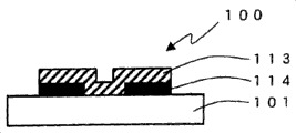
Fig. 1 is the diagrammatic cross-section of an embodiment of the expression photomask with gray scale of the present invention;
Fig. 2 is the diagrammatic cross-section of the manufacturing process of expression photomask with gray scale of the present invention shown in Figure 1;
Fig. 3 be expression then Fig. 2 of the present invention have the diagrammatic cross-section of manufacturing process of the photomask of gray scale;
Fig. 4 is the diagrammatic cross-section of other manufacturing processes of the expression photomask with gray scale of the present invention;
Fig. 5 be expression then Fig. 4 of the present invention have the diagrammatic cross-section of other manufacturing processes of the photomask of gray scale;
Fig. 6 is the figure of the transmissivity of one of expression photomask example;
Fig. 7 is the figure of the reflectivity of one of combination of expression photomask and semi-transparent film example;
Fig. 8 is the process profile that the problem points when using general photomask blank is described.
Embodiment
Below, have the photomask of gray scale and an embodiment of manufacture method thereof with reference to description of drawings is of the present invention.
Fig. 1 is the diagrammatic cross-section of an embodiment of the expression photomask with gray scale of the present invention.
Fig. 2 and after Fig. 3 be the diagrammatic cross-section of the manufacturing process of expression photomask with gray scale of the present invention shown in Figure 1.Fig. 4 and after Fig. 5 be the diagrammatic cross-section of other embodiments of the manufacturing process of the expression photomask with gray scale of the present invention.
(photomask) with gray scale
As shown in Figure 1, structure with photomask 100 of gray scale of the present invention is, on transparency carrier 101, has desirable pattern, the film that forms pattern is by the photomask pattern 114 that can not see through exposure light in fact, constitute with the semi-transparent film pattern 113 that sees through exposure light with desirable transmissivity, on transparency carrier 101, be mixed in stacked in order photomask pattern 114 and semi-transparent film pattern 113 and the lightproof area of existence, the translucent area that has only semi-transparent film pattern 113 to exist, and photomask pattern 114 and all non-existent regional transmission of semi-transparent film pattern 113.
Among the present invention, the photomask pattern that can not see through exposure light in fact is meant, in exposure wavelength, make exposure light transmission and the photonasty resist can not be by single exposure by the photomask pattern of sensitization, usually, in exposure wavelength, transmissivity is to be desirable below 0.1%.
Among Fig. 1, photomask pattern 114 and semi-transparent film pattern 113 is the stacked in order and lightproof area that exists by the semi-transparent film side behind the pattern etching, the position that becomes the edge part of the edge part of photomask pattern 114 and semi-transparent film pattern 113 is an identical construction.
In the photomask 100 with gray scale of the present invention, as transparency carrier 101, usually can use low-expansion glasses such as soda-lime glass, pyrex and aluminum silicate glass behind the optical grinding that is used for photomask, synthetic quartz glass, fluorite, calcium fluoride etc., at exposure light is under short wavelength's the situation, preferred synthetic quartz glass.
Among the present invention,,, then can use so long as can be used as the film that common mask material such as chromium mesentery, molybdenum silicide, tantalum, aluminium, silicon, monox, silicon oxynitride uses as the photomask that forms photomask pattern 114.On the cost of mask blank, quality, more preferably with the chromium that has most the achievement used chromium mesentery as major component.The chromium mesentery uses the monofilm that is selected from the material in chromium, chromium oxide, chromium nitride, the nitrogen chromium oxide usually, but in these chromium based materials, the chromium nitride film that chromium film that more preferably film forming is easy and versatility is high or membrane stress reduce easily.For example when being photomask, use with the thickness of 50nm~150nm extent and scope with chromium.
Among the present invention, as the semi-transparent film that forms semi-transparent film pattern 113, the oxide film of the photomask of the above-mentioned photomask pattern 114 of use formation, nitride film, carbonized film etc., but for keeping the advantage of available same etching machines, operation composition semi-transparent film and photomask, the material of preferred semiconductor film and photomask homology constitutes.When the as above such preferable material of conduct is used the chromium based material in described photomask, semi-transparent film is as long as use the higher film of transmissivity that contains aerobic, nitrogen, carbon etc. in the chromium, film formed and the reflectivity of thickness optimization when being laminated on the photomask with reduction gets final product.Chromium is in the semi-transparent film, more preferably the two characteristic of transmissivity and the anti-reflective function chromium oxide film or the nitrogen chromium oxide film that are easier to control.For example, when chromium oxide film is made semi-transparent film, use with the thickness of the scope of 5nm~150nm degree.When thickness during, be difficult to produce difference with respect to the transmissivity as semi-transparent film of photomask less than 5nm or greater than 150nm.Under the situation of the semi-transparent film that contains aerobic, nitrogen, carbon etc., owing to its absorbance changes because of composition, so by controlling thickness simultaneously and forming and to realize desirable transmissivity and anti-reflective function.
Among the present invention,, preferably form with 15%~85% scope with respect to the exposure optical transmission rate of the semi-transparent film that forms semi-transparent film pattern 113.At the translucent area that has only semi-transparent film to exist, transmissivity was less than 15% o'clock, when using the photomask with gray scale of the present invention to form the resist pattern, with lightproof area be difficult to produce poor, on the other hand, if transmissivity is greater than 85%, when then forming the resist pattern, with regional transmission be difficult to produce poor.
Among the present invention, the anti-reflective function of semi-transparent film of photomask with gray scale is with respect to the wavelength that at least one had in the g line (436nm) of the light of generations such as extra-high-pressure mercury vapour lamp, h line (405nm), i line (365nm), KrF excimer laser (248nm), the ArF excimer laser (193nm), has anti-reflective function, more preferably, all has anti-reflective function with respect to plural wavelength as g line, i line.
Usually, when forming the photomask pattern by metal films such as chromium, with respect to the exposure light, when photomask did not have anti-reflective function, reflectivity showed that parasitic light exerts an influence more than 30%.
Among the present invention, the exposure reflection of light rate of the lightproof area that exists with respect to stacked semi-transparent film pattern 113 on photomask pattern 114 is preferably less than 30%.If reflectivity is greater than 30%, then in the photoetching process of using photomask, parasitic light exerts an influence, and the exploring degree of photoresist is reduced, if reflectivity less than 30%, does not then have obstacle as anti-reflective function in practicality.
(manufacture method) with photomask of gray scale
Secondly, the embodiment to the manufacture method of the photomask with gray scale of the present invention describes.
(first embodiment)
Fig. 2 is the diagrammatic cross-section of the manufacturing process of expression photomask 100 with gray scale of the present invention shown in Figure 1, Fig. 3 be expression then Fig. 2 of the present invention have the diagrammatic cross-section of manufacturing process of the photomask 100 of gray scale.
Make the photomask with gray scale of present embodiment, at first prepared on transparency carrier 101 film forming as the photomask blank 103 (Fig. 2 (a)) of the photomask 102 of first film.If the photomask 102 of photomask blank 103 is chromium film or chromium nitride film, then chromium film or chromium nitride film form by sputtering method, use and can obtain easily as photomask blank usually.
Secondly, according to usual way above-mentioned photomask blank 103 is carried out primary mask pattern plate-making, composition is as the photomask 102 of first film.That is, the resist of the coating photonasty resist corresponding with the exposure device of laser explosure device etc. etc. on photomask 102 applies baking and banking up with earth that laggard professional etiquette fixes time, and forms the photomask usefulness resist film 104 (Fig. 2 (b)) of uniform thickness.
In addition, as the exposure device that mask is used, EB exposure device, laser explosure device are arranged.Can use among the present invention, but follow maximization, the multiple planeization when making of display device such as LCD and PDP, photomask also maximizes, thus the main laser explosure device that uses in the photomask that image-displaying member is used.
Secondly, utilize laser homenergic line 105 on the resist film on the photomask 104, to carry out pattern plotter (Fig. 2 (c)).In the present embodiment, this pattern plotter is only described in the mode that forms the border that the translucent area that forms in photomask zone and the subsequent handling directly joins, and the part of photomask 102 is carried out composition.Be used for the position that photomask is identical with semi-transparent film and carry out the pattern plotter of composition in the lump, when the plate-making of secondary mask pattern, carry out.
Carrying out this when describing, will contraposition be used when the composition of second layer semi-transparent film describe to use alignment mark, describe to dispose a plurality of (not shown) in the non-transfer area of mask.
Then, on the characteristic of the resist that uses, if bake and bank up with earth operation after being necessary then to add exposure, the developer solution of stipulating with resist develops, and washes, and forms photomask resist pattern 106 (Fig. 2 (d)).
Secondly,, form photomask pattern 107 (Fig. 2 (e)), residual resist is peeled off removed, obtain substrate 108 (Fig. 2 (f)) with the photomask pattern to carrying out etching with the photomask 102 that resist pattern 106 exposes from photomask.Photomask pattern 107 just forms the border that photomask zone and semi-transparent film zone directly join, and in this stage, the photomask at the position that etching is identical with semi-transparent film is partly not etched and residual.
The etching of photomask 102 can be used Wet-type etching or dry etching method, but as mentioned above, under the situation of the photomask that image-displaying member is used, follow the maximization of mask, dry-etching aspect device, material cost are too high, and large-area dry-etching worsens etch uniformity, therefore, and preferred Wet-type etching.At photomask 102 is under the situation of chromium mesentery, and preferred cerous nitrate is a wet etchant.
In the present embodiment, after the composition operation of having carried out first film,,, then can carry out the operation of defect correction if be necessary with the inspection of the substrate 108 of photomask pattern.When photomask uses the chromium mesentery, can use inspection technology, the correction technique of the photomask of existing chromium mesentery.Inspection operation by carrying out the inspection of photomask pattern dimension, pattern defect detection, if be necessary then to revise operation, prevent that defective substrate from being joined to subsequent processing, thereby help to improve yield rate, reduce the mask cost.
Secondly, on whole of the substrate 108 of being with the photomask pattern, semi-transparent film 109 is carried out film forming (Fig. 2 (g)).
At this, the preferred material with above-mentioned photomask 102 homologys of semi-transparent film 109.As mentioned above, if photomask 102 is made of above-mentioned chromium based material, then semi-transparent film 109 uses one or more and the higher film of transmissivity that contains aerobic, nitrogen, carbon etc. in the chromium, as long as the mode of the reflectivity when being laminated in photomask with reduction, film is formed and the thickness optimization gets final product.
Under the situation of the semi-transparent film that contains aerobic, nitrogen, carbon etc.,,, can realize desirable transmissivity and preventing reflection characteristic therefore by controlling thickness and composition simultaneously because its absorbance changes by composition.For example chromium oxide film is being made under the situation of semi-transparent film 109, using with the thickness of the scope of 5nm~150nm degree.
The film forming of semi-transparent film 109 is identical with the method that forms the chromium photomask, uses sputtering method equal vacuum film build method.
Secondly, by secondary mask pattern plate-making process, the semi-transparent film 109 as second film is carried out composition, the photomask pattern 107 of formation and lower floor carries out the semi-transparent film pattern after the contraposition.That is, the resist of the coating photonasty resist corresponding with the exposure device of laser explosure device etc. etc. is baked and banked up with earth the stipulated time after coating on semi-transparent film 109, forms semi-transparent film usefulness resist film 110 (Fig. 3 (h)).
Then, carry out the pattern plotter of semi-transparent film 109 with laser homenergic line 111.Carry out this when describing, detect the alignment mark of ground floor photomask, carry out contraposition (Fig. 3 (i)).Among the present invention, be located at the alignment mark on the photomask pattern 107, can easily detect, describe positional precision thereby improve via resist film 110.
Next, on the characteristic of the resist that uses, if bake and bank up with earth operation after being necessary then to add exposure, the developer solution of stipulating with resist develops, and washes, and forms semi-transparent film resist pattern 112 (Fig. 3 (j)).
Secondly, the semi-transparent film 109 that etching is exposed with resist pattern 112 from semi-transparent film is followed the photomask pattern 107 that etching is exposed, and forms semi-transparent film pattern 113 and photomask pattern 114 (Fig. 3 (k)).
At this, after having carried out the semi-transparent film etching, the etching photomask carries out composition once more at position that the photomask of lower floor exposes.Much less, the position of etched photomask is different with initial etched position once more.In addition, under the situation of the semi-transparent film that the material that uses with the photomask homology constitutes, carry out the etching of semi-transparent film and the etching of photomask with same etching solution serially, can shorten manufacturing process and enhance productivity, thus more preferably it.
In above-mentioned present embodiment, photomask forms the photomask pattern by the secondary pattern etching, but in the present invention, also can only carry out pattern etching once and forms the photomask pattern.
Secondly, use the stripper of resist special use etc., residual semi-transparent film is peeled off with resist pattern 112 removed, obtain having the photomask 100 (Fig. 3 (l)) of gray scale.Afterwards, carry out the inspection of mask, if be necessary then to revise.
Among Fig. 3 (l), an edge part after stacked semi-transparent film carries out pattern etching on the photomask, the position consistency ground of the section edges portion of photomask and semi-transparent film forms, and at another edge part of photomask pattern 114, ladder covers and forms semi-transparent film well.
(second embodiment)
Secondly, second embodiment is described.Second embodiment has been to use the manufacture method of the situation of the general photomask blank that sets in advance low reflection layer on photomask.
Fig. 4 and Fig. 5 then are the diagrammatic cross-sections of other manufacturing process of the expression photomask with gray scale of the present invention.
In the present embodiment,, prepare photomask 202 is set on transparency carrier 201, and carried out the photomask blank 220 (Fig. 4 (a)) of the two-layer structure of low-reflection film 203 film forming thereon for making the photomask with gray scale of the present invention.For example, the photomask 202 of photomask blank 220 is chromium nitride films, and low-reflection film 203 can be used as the material that photomask blank uses usually as chromium oxide film.
But, the low-reflection film 203 of above-mentioned photomask blank 220, owing to be not the function that possesses easily as the regulation of semi-transparent film, so in the membrane structure of original normally used photomask blank, can not obtain the photomask with gray scale of the present invention.
In the photomask with gray scale of the present invention, be mixed in stacked in order photomask and semi-transparent film on transparency carrier and the lightproof area that exists, have only translucent area that semi-transparent film exists, and photomask and all non-existent regional transmission of semi-transparent film.
Therefore, at first the 203 whole etchings of the low-reflection film on the photomask 202 are removed, obtain the substrate (Fig. 4 (b)) that photomask 202 is exposed.The etching of low-reflection film 203 can be controlled by etching solution and etching period.
Secondly, the aforesaid substrate that photomask 202 is exposed according to usual way carries out primary mask pattern plate-making, the part of composition photomask 202.That is, the resist of the coating photonasty resist corresponding with the exposure device of laser explosure device etc. etc. on photomask 202 applies baking and banking up with earth that laggard professional etiquette fixes time, and forms the photomask usefulness resist film 204 (Fig. 4 (c)) of uniform thickness.
Secondly, carry out the pattern plotter (Fig. 4 (d)) of photomask with laser homenergic line 205 with resist film 204.In the present embodiment, pattern plotter is described in the mode on the border that only forms the semi-transparent film zone that forms in photomask zone and the subsequent handling and directly join, and the part of photomask 202 is carried out composition.With the etched in the lump pattern plotter of the same area of photomask and semi-transparent film, when making a plate, secondary mask pattern carries out.
In addition, when carrying out above-mentioned describing, what be used for contraposition during with the composition of the semi-transparent film of the second layer describes to use alignment mark, describes to dispose a plurality of (not shown) in the non-transfer area of mask.
Then, on the characteristic of the resist that uses, if bake and bank up with earth operation after being necessary then to add exposure, the developer solution of stipulating with resist develops, and washes, and forms photomask resist pattern 206 (Fig. 4 (e)).
Secondly,, form photomask pattern 207 (Fig. 4 (f)), residual resist is peeled off removed, obtain substrate 208 (Fig. 4 (g)) with the photomask pattern to carrying out etching with the photomask 202 that resist pattern 206 exposes from photomask.Photomask pattern 207 just forms the border that photomask zone and semi-transparent film zone directly join, and in this stage, the photomask at the position that etching is identical with semi-transparent film is partly not etched and residual.
Such as in first embodiment narration, the etching of photomask 202 can be used Wet-type etching or dry etching method, preferred Wet-type etching.At photomask 202 is under the situation of chromium mesentery, and preferred cerous nitrate is a wet etchant.
In the present embodiment, after the composition operation of having carried out first film, with the inspection of the substrate 208 of photomask pattern, if be necessary then can carry out the operation of defect correction.When in photomask 202, using the chromium mesentery, can use inspection technology, the correction technique of the photomask of existing chromium mesentery.By carry out this inspection operation, if be necessary then to revise operation, can prevent that defective substrate from being joined to subsequent processing.
Secondly, film forming semi-transparent film 209 (Fig. 5 (h)) on whole of the substrate 208 of being with the photomask pattern.In second embodiment, the material of semi-transparent film, film build method, characteristic are all identical with first embodiment.
Secondly,, the semi-transparent film 209 and first film as second film are carried out composition, form the semi-transparent film pattern that has carried out contraposition with lower floor's photomask pattern by carrying out secondary mask pattern plate-making process.That is, the resist of the coating photonasty resist corresponding with the exposure device of laser explosure device etc. etc. is baked and banked up with earth the stipulated time after the coating on semi-transparent film 209, forms semi-transparent film usefulness resist film 210 (Fig. 5 (i)).
Then, carry out the pattern plotter of semi-transparent film with laser homenergic line 211 with resist film 210.Carry out this when describing, detect the alignment mark of ground floor photomask, carry out contraposition (Fig. 5 (j)).
Next, on the characteristic of the resist that uses, if bake and bank up with earth operation after being necessary then to add exposure, the developer solution of stipulating with resist develops, and washes, and forms semi-transparent film resist pattern 212 (Fig. 5 (k)).
Secondly, to carrying out etching with the photomask 209 that resist pattern 212 exposes from photomask, then, under the situation that the photomask pattern 207 of lower floor exposes, further this position of etching continuously forms semi-transparent film pattern 213 and photomask pattern 214 (Fig. 5 (l)) thus.In the present embodiment, because photomask and semi-transparent film use the material of homology, thereby available same technology is carried out the composition of photomask and semi-transparent film together, thus more preferably it.
In the present embodiment, photomask forms the photomask pattern by the secondary pattern etching, but in the present invention, also can only carry out pattern etching once and forms the photomask pattern.
Secondly, residual semi-transparent film peeled off with resist pattern 212 remove, obtain having the photomask 200 (Fig. 5 (m)) of gray scale.Afterwards, carry out the inspection of mask, if be necessary then to revise.
Among Fig. 5 (m), and the photomask zone that exist stacked at photomask pattern 214 and semi-transparent film pattern 213 by the stacked side behind the pattern etching, photomask pattern 214 and the same technology of semi-transparent film pattern 213 usefulness are carried out etching together, therefore, the position that becomes the edge part of the edge part of photomask pattern 214 and semi-transparent film pattern 213 is roughly the same structure.
In addition, in the present invention, about the transmissivity of semi-transparent film and the control of reflectivity, as mentioned above, the transmissivity of semi-transparent film need be controlled at 15~85%, reflectivity that will the lightproof area that stacked semi-transparent film forms on photomask is controlled at less than 30%.Satisfy the semi-transparent film and the photomask of such condition, the selection by each membranous adjustment and thickness thereof realizes.As one of semi-transparent film example, as mentioned above, chromium oxide is arranged, as one of photomask example, the crome metal film is arranged.With regard to membranous adjustment, when being semi-transparent film, adjust the degree of oxidation of chromium oxide etc. by the change sputtering condition.When being photomask, there are some additives to be added.For example known use nitrogen.Perhaps, change its density.Usually change sputtering condition and change crystallinity (particle diameter) or in film, mix space (bubble), regulate apparent n (refractive index), k (extinction coefficient (Extinction Coefficient)) thus.
It is that photomask, thickness are 70nm that Fig. 6, Fig. 7 represent respectively with crome metal film (n=2.4, k=3.1), with chromium oxide film (n=2.8, k=0.3) be semi-transparent film, the transmissivity with respect to g line (436nm) (semi-transparent film) when thickness is changed with 0~100nm and the relation of reflectivity (photomask+semi-transparent film).See among Fig. 6 that will obtain under the situation that transmissivity is 40% translucent area, the thickness of semi-transparent film is 50nm, but that the reflectivity of the photomask of this moment is seen as in Fig. 7 is about 21%, is better low reflection.On the other hand, the expectation transmissivity is 80% o'clock, and the thickness of semi-transparent film is about 5nm, and the light shielding part reflectivity is 34%, becomes not too good low conditioned reflex.Under this situation, need to change photomask and semi-transparent film membranous, change n and k.
In the above description, the chromium mesentery is used as material, but in addition,, then can use so long as molybdenum silicide, tantalum, aluminium, silicon, monox, silicon oxynitride etc. be can be used as the film that common mask material uses.
In addition,, the mask of 2 gray scales is illustrated the greyscale photo mask of the invention described above, but also can be by with plate-making, film forming, plate-making repeats to realize the photomask of the many gray scales more than 2 gray scales again.
Embodiment
(embodiment 1)
On film forming on the synthetic quartz substrate of 330 * 450nm behind the optical grinding is had an appointment the photomask blank commonly used of the photomask that is made of chromium of 100nm, the commercially available photoresist of the about 380nm of coating (the system ip-3500 of chemical industry society is answered in Tokyo), after on the hot plate that is heated to 120 degree, baking and banking up with earth 15 minutes, describe desirable photomask pattern with the system LRS11000-TFT3 of laser drawing apparatus マ イ Network ロ ニ Star Network society with photomask.At this pattern of describing is to be used for the final pattern of shading fully.
Secondly, develop, obtain photomask resist pattern with special-purpose developer (the system NMD3 of chemical industry society is answered in Tokyo).
Secondly, be the etching mask with the resist pattern, the chromium film is carried out etching, and then remaining resist pattern is peeled off, obtain desirable photomask pattern thus.In addition, the commercially available cerous nitrate of the etching of chromium film use is wet etchant (the system MR-ES of ザ イ Application Network テ Star Network society).The etching period of chromium film is about 60 seconds.
Secondly, to the pattern correction that the substrate of the band photomask pattern that obtains like this carries out the inspection of photomask pattern dimension, pattern defect detection, carries out as required, after further cleaning, be chromium oxide film with the sputtering film-forming semi-transparent film.The thickness of chromium oxide film is about 30nm, and transmissivity is about 40% (wavelength g line: 436nm).This semi-transparent film has anti-reflective function, and the zone that photomask and semi-transparent film constitute shows as the reflectivity less than 30% in the g line.
Secondly, the commercially available photoresist of the about 380nm of coating (Tokyo answers chemical industry society to make ip-3500) once more thereon, and being heated on 120 ℃ the hot plate, baked and banked up with earth 15 minutes.
Then, describe to become the image of semi-transparent film pattern once more, develop, obtain photomask resist pattern with special-purpose developer (Tokyo answers chemical industry society to make NMD3) with laser drawing apparatus (マ イ Network ロ ニ Star Network society system LRS11000-TFT3).In addition, drawing apparatus LRS11000 has aligning and describes function, to established photomask pattern aligned position, forms the semi-transparent film pattern.
Secondly, be mask with the resist pattern, be wet etchant (the system MR-ES of ザ イ Application Network テ Star Network society) etching semi-transparent film with commercially available cerous nitrate, then, the photomask that exposes is carried out etching, obtain semi-transparent film pattern and final etched photomask pattern.
At last, residual resist is peeled off, via inspection operations such as pattern dimension inspection, defect inspections, carry out the pattern correction as required, obtained having the photomask of desirable gray scale.
(embodiment 2)
Preparation forms the chromium nitride film as photomask on the synthetic quartz substrate of 330 * 450nm behind the optical grinding, and is provided with the commercially available photomask blank as the two-layer structure of the chromium oxide film of low-reflection film thereon.The thickness of chromium nitride film is 70nm, and the thickness of chromium oxide film is about 20nm.
Secondly, be wet etchant (the system MR-ES of ザ イ Application Network テ Star Network society) with commercially available cerous nitrate, be that the substrate of the photomask that obtains exposing is removed in the whole etchings of chromium oxide film with the low-reflection film of above-mentioned blank.
Secondly, the commercially available photoresist of the about 380nm of coating on the above-mentioned photomask that exposes (the system ip-3500 of chemical industry society is answered in Tokyo), and baked and banked up with earth 15 minutes being heated on 120 ℃ the hot plate, describe desirable photomask pattern with photomask with laser drawing apparatus (the system LRS11000-TFT3 of マ イ Network ロ ニ Star Network society) afterwards.
Secondly, develop, obtain photomask resist pattern with special-purpose developer (the system NMD3 of chemical industry society is answered in Tokyo).
Secondly, is the etching mask with photomask with the resist pattern, is wet etchant (the system MR-ES of ザ イ Application Network テ Star Network society) etching photomask with commercially available cerous nitrate, forms the photomask pattern, residual resist peeled off remove, obtain substrate with the photomask pattern.
Secondly, to the pattern dimension inspection of the substrate that carries out above-mentioned band photomask pattern, pattern defect detection, the pattern correction carried out as required, after further cleaning, be chromium oxide film with the sputtering film-forming semi-transparent film.The thickness of chromium oxide film is about 20nm, and transmissivity is about 30% (wavelength i line: 365nm).This semi-transparent film has anti-reflective function, and the zone that photomask and semi-transparent film constitute shows as the reflectivity less than 30% on the i line.
Secondly, apply the commercially available photoresist (the system ip-3500 of chemical industry society is answered in Tokyo) of about 380nm once more, and baked and banked up with earth 15 minutes being heated on 120 ℃ the hot plate, photomask is described desirable semi-transparent film pattern with laser drawing apparatus (the system LRS11000-TFT3 of マ イ Network ロ ニ Star Network society) afterwards.
Secondly, with the resist pattern is the etching mask, with commercially available cerous nitrate is wet etchant (the system MR-ES of ザ イ Application Network テ Star Network society) etching nitrogen chromium oxide film, then, the photomask that exposes is carried out etching, and then peel off residual resist picture, obtain desirable semi-transparent film pattern and photomask pattern thus.
Secondly, via inspections operations such as pattern dimension inspection, defect inspections, also carry out the pattern correction as required, obtain desirable photomask with gray scale.
Claims (10)
1. photomask with gray scale, on transparency carrier, has desirable pattern, and the film that forms described pattern is by the photomask that can not see through exposure light in fact, constitute with the semi-transparent film that sees through described exposure light with desirable transmissivity, the lightproof area that on described transparency carrier, is mixed in stacked in order described photomask and described semi-transparent film and exists, the translucent area that has only described semi-transparent film to exist, and described photomask and all non-existent regional transmission of described semi-transparent film, it is characterized in that
Described semi-transparent film has anti-reflective function with respect to described exposure light.
2. the photomask with gray scale as claimed in claim 1 is characterized in that,
Have only translucent area that described semi-transparent film exists with respect to described exposure optical transmission rate in 15%~85% scope.
3. the photomask with gray scale as claimed in claim 1 or 2 is characterized in that,
Stacked in order described photomask and described semi-transparent film and the lightproof area that exists with respect to described exposure reflection of light rate less than 30%.
4. as each described photomask in the claim 1~3, it is characterized in that with gray scale,
Described semi-transparent film has anti-reflective function with respect to the wavelength that at least one had in g line, h line, i line, KrF excimer laser, the ArF excimer laser.
5. as each described photomask in the claim 1~4, it is characterized in that with gray scale,
Described photomask and described semi-transparent film all are major component with chromium.
6. the photomask with gray scale as claimed in claim 5 is characterized in that,
Described photomask is made of chromium or chromium nitride, and described semi-transparent film is made of chromium oxide or nitrogen chromium oxide.
7. method for making with photomask of gray scale, described photomask with gray scale has desirable pattern on transparency carrier, and the film that forms described pattern constitutes by the photomask that can not see through exposure light in fact with the semi-transparent film of desirable transmissivity through described exposure light, this method for making with photomask of gray scale is characterised in that
Comprise in order:
Preparation on described transparency carrier film forming the operation of mask blank of described photomask;
The operation of the described photomask of composition;
On the described transparency carrier of the photomask after being provided with described composition, film forming has the operation of the semi-transparent film of anti-reflective function with respect to described exposure light comprehensively;
Composition has the operation of the semi-transparent film of described anti-reflective function.
8. method for making with photomask of gray scale, described photomask with gray scale has desirable pattern on transparency carrier, and the film that forms described pattern constitutes by the photomask that can not see through exposure light in fact with the semi-transparent film of desirable transmissivity through described exposure light, this method for making with photomask of gray scale is characterised in that
Comprise in order:
Preparation has the operation of mask blank of the two membranes of photomask and low-reflection film on described transparency carrier;
Remove the operation that described low-reflection film exposes described photomask by etching;
The operation of the described photomask of composition;
On the described transparency carrier of the photomask after being provided with described composition, film forming has the operation of the semi-transparent film of anti-reflective function comprehensively;
Composition has the operation of the semi-transparent film of described anti-reflective function.
9. as claim 7 or 8 described method for makings, it is characterized in that, comprising with photomask of gray scale:
After composition has the operation of semi-transparent film of described anti-reflective function, the operation of the described photomask that exposes of composition once more.
10. as each described method for making in the claim 7~9, it is characterized in that with photomask of gray scale,
After the operation of the described photomask of composition, the mask pattern that carries out described photomask is checked operation, is reached the correction operation of carrying out as required.
Applications Claiming Priority (2)
| Application Number | Priority Date | Filing Date | Title |
|---|---|---|---|
| JP2005273601 | 2005-09-21 | ||
| JP273601/2005 | 2005-09-21 |
Publications (1)
| Publication Number | Publication Date |
|---|---|
| CN101268417A true CN101268417A (en) | 2008-09-17 |
Family
ID=37888972
Family Applications (1)
| Application Number | Title | Priority Date | Filing Date |
|---|---|---|---|
| CNA2006800345852A Pending CN101268417A (en) | 2005-09-21 | 2006-09-19 | Photomask having gray scale and method of manufacturing the same |
Country Status (5)
| Country | Link |
|---|---|
| US (1) | US8124301B2 (en) |
| KR (1) | KR20080037702A (en) |
| CN (1) | CN101268417A (en) |
| TW (1) | TW200717176A (en) |
| WO (1) | WO2007034930A1 (en) |
Cited By (8)
| Publication number | Priority date | Publication date | Assignee | Title |
|---|---|---|---|---|
| CN102103323B (en) * | 2009-12-21 | 2012-10-10 | 北京京东方光电科技有限公司 | Half-tone mask plate and manufacturing method thereof |
| CN102308256B (en) * | 2009-02-16 | 2013-09-25 | 大日本印刷株式会社 | Photomask and methods for manufacturing and correcting photomask |
| TWI502623B (en) * | 2010-01-07 | 2015-10-01 | Hoya Corp | Method of manufacturing a photomask, photomask, and method of manufacturing a display device |
| CN104155810B (en) * | 2014-07-22 | 2017-01-25 | 京东方科技集团股份有限公司 | Mask |
| CN111095108A (en) * | 2017-07-17 | 2020-05-01 | Asml荷兰有限公司 | Information determination apparatus and method |
| CN111367142A (en) * | 2018-12-26 | 2020-07-03 | 聚灿光电科技(宿迁)有限公司 | Novel optical mask plate with different light transmission |
| CN113296354A (en) * | 2020-02-22 | 2021-08-24 | 长鑫存储技术有限公司 | Mask plate applied to semiconductor photoetching process and photoetching process method |
| CN113311660A (en) * | 2021-06-03 | 2021-08-27 | 上海传芯半导体有限公司 | Mask base plate manufacturing method and gluing equipment with plasma heating device |
Families Citing this family (20)
| Publication number | Priority date | Publication date | Assignee | Title |
|---|---|---|---|---|
| TWI446105B (en) * | 2007-07-23 | 2014-07-21 | Hoya Corp | Method of manufacturing a photomask, method of transferring a pattern, photomask and database |
| CN101393385B (en) * | 2007-09-21 | 2013-09-11 | 北京京东方光电科技有限公司 | Transmittance-adjustable half tone mask and method for manufacturing same |
| JP4934237B2 (en) * | 2007-09-29 | 2012-05-16 | Hoya株式会社 | Gray-tone mask manufacturing method, gray-tone mask, and pattern transfer method |
| US8685596B2 (en) * | 2007-12-04 | 2014-04-01 | Sharp Laboratories Of America, Inc. | Semi-transparent film grayscale mask |
| JP5108551B2 (en) * | 2008-02-15 | 2012-12-26 | Hoya株式会社 | Multi-tone photomask and pattern transfer method using the same |
| KR101079161B1 (en) * | 2008-12-22 | 2011-11-02 | 엘지이노텍 주식회사 | Half tone mask and fabricating method |
| CN101990058A (en) * | 2009-07-30 | 2011-03-23 | 鸿富锦精密工业(深圳)有限公司 | Method of coating wafer-level camera module and wafer-level camera module |
| DE102009046878A1 (en) * | 2009-07-31 | 2011-02-03 | Advanced Mask Technology Center Gmbh & Co. Kg | Reduction of ion migration of absorber materials of lithographic masks by chromium passivation |
| WO2012005524A2 (en) | 2010-07-08 | 2012-01-12 | Lg Innotek Co., Ltd. | The printed circuit board and the method for manufacturing the same |
| KR101679721B1 (en) | 2010-12-13 | 2016-11-28 | 삼성전자주식회사 | A photomask and methods of manufacturing the photomask |
| JP6021365B2 (en) * | 2012-03-12 | 2016-11-09 | キヤノン株式会社 | Imprint apparatus and article manufacturing method using the same |
| KR101823276B1 (en) * | 2013-09-24 | 2018-01-29 | 호야 가부시키가이샤 | Method for manufacturing transfer mask, and method for manufacturing semiconductor device |
| KR102157644B1 (en) * | 2014-08-13 | 2020-09-21 | (주)에스앤에스텍 | Milti-Gray Scale Photomask and manufacturing mathod thereof |
| KR102286886B1 (en) * | 2014-11-18 | 2021-08-09 | 삼성디스플레이 주식회사 | Photo mask and method of manufacturing the same |
| KR102502202B1 (en) | 2015-06-29 | 2023-02-21 | 삼성디스플레이 주식회사 | Light emitting display device and fabricating of the same |
| GB201517273D0 (en) * | 2015-09-30 | 2015-11-11 | Univ Manchester | Resist composition |
| US20170147652A1 (en) * | 2015-11-19 | 2017-05-25 | Institute For Information Industry | Search servers, end devices, and search methods for use in a distributed network |
| CN107145035A (en) * | 2017-03-30 | 2017-09-08 | 惠科股份有限公司 | Photomask and manufacturing method of active switch array substrate thereof |
| CN118192160A (en) * | 2017-07-21 | 2024-06-14 | 卡尔蔡司Smt有限责任公司 | Method and apparatus for processing excess material of a lithographic mask |
| US10811492B2 (en) | 2018-10-31 | 2020-10-20 | Texas Instruments Incorporated | Method and device for patterning thick layers |
Family Cites Families (6)
| Publication number | Priority date | Publication date | Assignee | Title |
|---|---|---|---|---|
| TW517286B (en) * | 2000-12-19 | 2003-01-11 | Hoya Corp | Gray tone mask and method for producing the same |
| KR100599054B1 (en) * | 2001-04-11 | 2006-07-12 | 삼성전자주식회사 | Transmittance Adjustment Mask and Method for Manufacturing thereof |
| DE10310136B4 (en) * | 2003-03-07 | 2007-05-03 | Infineon Technologies Ag | Mask set for the projection of pattern patterns arranged on the masks of the sentence and matched to one another on a semiconductor wafer |
| JP2005091855A (en) * | 2003-09-18 | 2005-04-07 | Dainippon Printing Co Ltd | Method for manufacturing gradation mask |
| JP4608882B2 (en) * | 2003-12-22 | 2011-01-12 | セイコーエプソン株式会社 | Exposure mask, method for manufacturing the same, and method for manufacturing a liquid crystal device |
| JP2005241693A (en) * | 2004-02-24 | 2005-09-08 | Shin Etsu Chem Co Ltd | Halftone phase shift mask blank, its manufacturing method and halftone phase shift mask and its manufacturing method |
-
2006
- 2006-09-19 WO PCT/JP2006/318892 patent/WO2007034930A1/en active Application Filing
- 2006-09-19 KR KR1020087005601A patent/KR20080037702A/en active Search and Examination
- 2006-09-19 CN CNA2006800345852A patent/CN101268417A/en active Pending
- 2006-09-19 TW TW095134519A patent/TW200717176A/en unknown
- 2006-09-19 US US12/066,203 patent/US8124301B2/en active Active
Cited By (9)
| Publication number | Priority date | Publication date | Assignee | Title |
|---|---|---|---|---|
| CN102308256B (en) * | 2009-02-16 | 2013-09-25 | 大日本印刷株式会社 | Photomask and methods for manufacturing and correcting photomask |
| CN102103323B (en) * | 2009-12-21 | 2012-10-10 | 北京京东方光电科技有限公司 | Half-tone mask plate and manufacturing method thereof |
| TWI502623B (en) * | 2010-01-07 | 2015-10-01 | Hoya Corp | Method of manufacturing a photomask, photomask, and method of manufacturing a display device |
| CN104155810B (en) * | 2014-07-22 | 2017-01-25 | 京东方科技集团股份有限公司 | Mask |
| CN111095108A (en) * | 2017-07-17 | 2020-05-01 | Asml荷兰有限公司 | Information determination apparatus and method |
| CN111367142A (en) * | 2018-12-26 | 2020-07-03 | 聚灿光电科技(宿迁)有限公司 | Novel optical mask plate with different light transmission |
| CN113296354A (en) * | 2020-02-22 | 2021-08-24 | 长鑫存储技术有限公司 | Mask plate applied to semiconductor photoetching process and photoetching process method |
| CN113296354B (en) * | 2020-02-22 | 2023-04-07 | 长鑫存储技术有限公司 | Mask plate applied to semiconductor photoetching process and photoetching process method |
| CN113311660A (en) * | 2021-06-03 | 2021-08-27 | 上海传芯半导体有限公司 | Mask base plate manufacturing method and gluing equipment with plasma heating device |
Also Published As
| Publication number | Publication date |
|---|---|
| TWI363247B (en) | 2012-05-01 |
| WO2007034930A1 (en) | 2007-03-29 |
| US8124301B2 (en) | 2012-02-28 |
| US20090220867A1 (en) | 2009-09-03 |
| KR20080037702A (en) | 2008-04-30 |
| TW200717176A (en) | 2007-05-01 |
Similar Documents
| Publication | Publication Date | Title |
|---|---|---|
| CN101268417A (en) | Photomask having gray scale and method of manufacturing the same | |
| JP5244485B2 (en) | Photomask, manufacturing method thereof, and pattern transfer method | |
| TWI387845B (en) | Gray tone mask and pattern transfer method | |
| CN101788757B (en) | Multi-color light adjustment mask, its manufacture method and a pattern transfer-printing method | |
| CN103383522A (en) | Photo mask, pattern transfer method and flat panel display manufacturing method | |
| CN101408725A (en) | Method for manufacturing grey mask, grey mask and pattern transfer print method | |
| JP5196098B2 (en) | Photomask having gradation and method for manufacturing the same | |
| CN106547167A (en) | Photo blanks, preparation method and photomask | |
| JP2014066863A5 (en) | ||
| JP4468093B2 (en) | Gradation photomask manufacturing method | |
| JP4714311B2 (en) | Multi-tone photomask manufacturing method and pattern transfer method for thin film transistor substrate | |
| JP4816349B2 (en) | Gradation mask | |
| CN101963753B (en) | Multi-color photomask and method of manufacturing the same, and pattern transfer method | |
| JP2012008546A (en) | Method for manufacturing multilevel gradation photomask and method for transferring pattern | |
| JP2007171651A (en) | Method for correcting defect in photomask having gradation, and photomask having gradation | |
| TWI422963B (en) | Multi-tone photomask and method of manufacturing the same, and pattern transfer method | |
| JP2008065139A (en) | Grayscale mask | |
| JP2009237419A (en) | Multi-gradation photomask, manufacturing method thereof, and pattern transfer method | |
| JP4615032B2 (en) | Multi-tone photomask manufacturing method and pattern transfer method | |
| JP4848071B2 (en) | 5-tone photomask manufacturing method and pattern transfer method | |
| JP4797729B2 (en) | Defect correction method for semi-transparent region of photomask with gradation | |
| KR20090016113A (en) | Halftone blankmask and halftone slit mask using the same, and manufacturing method thereof | |
| KR20100056981A (en) | Multi-gray scale photomask and manufacturing method thereof | |
| JP4792148B2 (en) | 5-tone photomask manufacturing method and pattern transfer method | |
| JP4615066B2 (en) | Multi-tone photomask manufacturing method and pattern transfer method |
Legal Events
| Date | Code | Title | Description |
|---|---|---|---|
| C06 | Publication | ||
| PB01 | Publication | ||
| C10 | Entry into substantive examination | ||
| SE01 | Entry into force of request for substantive examination | ||
| RJ01 | Rejection of invention patent application after publication |
Application publication date: 20080917 |