Embodiment
Below, with the embodiment of description of drawings display device of the present invention and manufacturing approach thereof.
(embodiment 1)
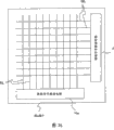
Fig. 1 is the structural drawing that is illustrated in an embodiment of the circuit that forms on the liquid crystal display area of face of liquid crystal side of a substrate SUB1 in across liquid crystal and relatively each substrate of configuration of liquid crystal indicator.
In Fig. 1; The signal line GL that has on the y direction source signal line SL that extends and be set up in parallel along the x direction and extend on the x direction with this source signal line SL insulation and be set up in parallel along the y direction, the rectangular area that is surrounded by this each signal wire is equivalent to the zone (the with dashed lines frame illustrates among the figure) of pixel.Thus, each pixel is rectangular configuration and constitutes above-mentioned liquid crystal display area by this pixel groups.
In the zone of each pixel, on its most of zone, form the pixel electrode PX for example constitute by transparency electrode, this pixel electrode PX through thin film transistor (TFT) TFT for example with in the drawings on the left of the source signal line SL of adjacency be connected.This thin film transistor (TFT) TET controls and will provide or not provide to pixel electrode PX from the signal of source signal line SL through its conducting, the driving that ends.
Above-mentioned thin film transistor (TFT) TFT; The gate electrode GT that will be formed by the extension of above-mentioned signal line GL is configured in the top of semiconductor layer, forms MIS (the Metal Insulator Semiconductor: structure metal-insulator semiconductor) that is called as so-called top grid type.
Thus; Through to each signal line GL signal (sweep signal) being provided respectively successively; Make the thin film transistor (TFT) TFT conducting of each pixel of pel array; And sub image signal is supplied with each source signal line SL indescribably according to the moment of its conducting, thereby the voltage of this picture signal is put on the pixel electrode PX of each pixel of above-mentioned pel array.
In addition; Liquid crystal indicator shown in this embodiment; Also has another not shown piece substrate across liquid crystal configurations with aforesaid substrate SUB1; On the face of the liquid crystal side of this substrate, form the opposite electrode public to each pixel, this opposite electrode for example is made up of transparency electrode, and the signal that the signal (picture signal) of supplying with above-mentioned source signal line SL is become the voltage of benchmark is provided.Above-mentioned liquid crystal is applied the electric field by the potential difference (PD) generation of pixel electrodes PX and opposite electrode, so that the molecular motion of this liquid crystal.
(a) of Fig. 2 extracts a pixel in each pixel shown in Fig. 1 out draw figure.In addition, Fig. 2 (b) is the cut-open view of b-b line of Fig. 2 (a).
In Fig. 2; The ST of source region portion of source signal line SL, thin film transistor (TFT) TFT, the CH of channel region portion (gate electrode GT under part), the DT of drain region portion and pixel electrode PX, at first the first transparent oxide layer TOX1 by integrally formed identical layer forms.
Promptly; In this first transparent oxide layer TOX1; The above-mentioned channel region CH of portion forms low and the film (semiconductor layer) that sheet resistance is high of carrier concentration; The formation zone of the ST of source region portion, the DT of drain region portion and the pixel electrode PX of source signal line SL, thin film transistor (TFT) TFT forms the carrier concentration height and the low film (conductor layer) of sheet resistance.In this case; For example; Can form sheet resistance is uprised according to the order of source signal line SL, the pixel electrode PX<ST of source region portion, the DT of drain region portion<CH of channel region portion, the order that also can form according to source signal line SL<pixel electrode PX, the ST of source region portion, the DT of drain region portion<CH of channel region portion uprises.In the latter case, when forming pixel electrode PX, can realize making its carrier concentration lower and do not damage the effect of its transparency.
The source signal line SL and the pixel electrode PX that constitute in a manner described integrally and at identical layer are formed by the first transparent oxide layer TOX1, therefore can both intervals (illustrating with w among the figure) be reduced to Min..This is because when when in different operations, forming source signal line SL respectively and compare with the situation of pixel electrode PX, can solve the restriction that the boundary because of mask registration is caused both interval increasings.Therefore, can improve aperture ratio of pixels.
The gate electrode GT of signal line GL and thin film transistor (TFT) TFT, for example by ITO (Indium Tin Oxide: tin indium oxide) or the second transparent oxide layer TOX2 of the low zinc paste (ZnO) of carrier concentration height and sheet resistance etc. integrally and at identical layer form.In this case, signal line GL and gate electrode GT are not limited to aforesaid transparent oxide layer, for example also can be formed by metal level.Its reason is, it is suitable when wanting further to reduce the resistance of signal line GL, adopting the metal level of the material suitable with it.
In addition, the above-mentioned first transparent oxide layer TOX1 forms on the surface of substrate SUB1, and its surface is covered by dielectric film GI, and above-mentioned gate electrode GT is configured in the top of the CH of channel region portion of the above-mentioned first nesa coating TOX1 across above-mentioned dielectric film GI.Above-mentioned dielectric film GI plays a part the gate insulating film of thin film transistor (TFT) TFT.
As stated, the above-mentioned first transparent oxide layer TOX1 forms high zone of carrier concentration and the low zone of carrier concentration by area dividing, the former is formed conductor layer, and the latter is formed semiconductor layer.Therefore, before the manufacturing approach of the above-mentioned liquid crystal indicator of explanation, explanation earlier zone that carrier concentration is high and low area dividing in transparent oxide layer TOX are opened and several embodiment when forming selectively.
Fig. 3 is the figure that is illustrated in the embodiment when forming high regional of carrier concentration in the transparent oxide layer TOX that forms on the surface of substrate SUB1 selectively.
In (a) of Fig. 3, on the surface of substrate SUB1, form transparent oxide layer TOX, on the zone in addition, zone that carrier concentration is increased in the surperficial zone of this transparent oxide layer TOX, for example form photoresist film PRT as mask.
Then, make laser RL shine above-mentioned transparent oxide layer TOX.For example preferably use the KrF excimer laser as this laser RL, but also can be other light source.Thus, the zone of the transparent oxide layer TOX that exposes from this photoresist film PRT can form and undertaken crystalline modified and zone that improved carrier concentration by this light.
Another embodiment when (b) of Fig. 3 illustrates and form high regional of carrier concentration in the transparent oxide layer TOX selectively through being radiated at of light; Be with the situation difference of Fig. 3 (a); On the surface of transparent oxide layer TOX, be pre-formed dielectric film GI, and passed through this dielectric film GI above-mentioned transparent oxide layer TOX irradiating laser RL.
Another embodiment when (c) of Fig. 3 illustrates and form high regional of carrier concentration in the transparent oxide layer TOX selectively through being radiated at of light; Be with the situation difference of Fig. 3 (b); Cover transparent oxide layer TOX with dielectric film GI; Will the for example electrode TM that forms on a part of zone of this dielectric film GI be layered in photoresist film PRT on this electrode TM as mask, and make laser RL irradiation transparent oxide layer TOX.
Another embodiment when (d) of Fig. 3 illustrates and form high regional of carrier concentration in the transparent oxide layer TOX selectively through being radiated at of light; Be with the situation difference of Fig. 3 (c); After the photoresist film PRT that is used to form electrode TM shown in Fig. 3 (c) removed with above-mentioned electrode TM as mask, to transparent oxide layer TOX irradiating laser RL.
Fig. 4 is the figure that is illustrated in another embodiment when forming high regional of carrier concentration in the transparent oxide layer TOX that forms on the surface of substrate SUB1 selectively.
In (a) of Fig. 4, on the surface of substrate SUB1, form transparent oxide layer TOX, making on the zone beyond the zone that carrier concentration improves in the zone on the surface of this transparent oxide layer TOX for example forms photoresist film PRT as mask.
Then, under the state of photoresist film PRT being stayed on the transparent oxide layer TOX, in reducing medium atmosphere, carry out thermal annealing.
Thus, the zone of the transparent oxide layer TOX that exposes from this photoresist film PRT can form and undertaken crystalline modified and zone that improved carrier concentration by this thermal annealing.
Another embodiment when (b) of Fig. 4 illustrates and in transparent oxide layer TOX, form high regional of carrier concentration selectively through thermal annealing; Be with the situation difference of Fig. 4 (a), under the state that remains with dielectric film GI that is selectively forming on the surface of transparent oxide layer TOX and the photoresist film PRT that when forming on the surface of this dielectric film GI and forming this dielectric film GI selectively, uses, carry out thermal annealing.
Another embodiment when (c) of Fig. 4 illustrates and in transparent oxide layer TOX, form high regional of carrier concentration selectively through thermal annealing; Be with the situation difference of Fig. 4 (b), carry out thermal annealing under the state of the photoresist film PRT that when forming on duplexer that remains with the dielectric film GI that selectively forming on the surface of transparent oxide layer TOX and electrode TM and the surface and forming this electrode TM and dielectric film GI, uses at this duplexer.
Another embodiment when (d) of Fig. 4 illustrates and in transparent oxide layer TOX, form high regional of carrier concentration selectively through thermal annealing; Be with the situation difference of Fig. 4 (c), carry out thermal annealing under the state that the photoresist film PRT that in the time will being formed with the duplexer of the dielectric film GI that selectively on the surface of transparent oxide layer TOX, forms and electrode TM, will use removes.
Fig. 5 is the figure that is illustrated in another embodiment when forming high regional of carrier concentration in the transparent oxide layer TOX that forms on the surface of substrate SUB1 selectively.
In (a) of Fig. 5, on the surface of substrate SUB1, form transparent oxide layer TOX, on the zone in addition, zone that carrier concentration is improved in the surperficial zone of this transparent oxide layer TOX, for example form photoresist film PRT as mask.
Then, implanting impurity ion NPI in above-mentioned transparent oxide layer TOX.As this foreign ion NPI, use N type or P type as required.
Thus, the zone of the transparent oxide layer TOX that exposes from this photoresist film PRT can form the zone that the injection through this foreign ion NPI has improved carrier concentration.
(b) of Fig. 5 illustrates through the injection of foreign ion NPI in transparent oxide layer TOX another embodiment when forming high regional of carrier concentration, and wherein transparent oxide layer TOX is formed on the surface of substrate SUB1.Be with the situation difference of Fig. 5 (a), on the surface of transparent oxide layer TOX, be pre-formed dielectric film GI, and above-mentioned transparent oxide layer TOX carried out the injection of foreign ion NPI through this dielectric film GI.
Another embodiment when (c) of Fig. 5 illustrates and form high regional of carrier concentration through being infused in the transparent oxide layer TOX of foreign ion NPI; Be with the situation difference of Fig. 5 (b); Cover transparent oxide layer TOX with dielectric film GI; Will the for example electrode TM that forms on a part of zone of this dielectric film GI be layered in photoresist film PRT on this electrode TM as mask, above-mentioned transparent oxide layer TOX carried out the injection of foreign ion NPI.
Another embodiment when (d) of Fig. 5 illustrates and form high regional of carrier concentration through being infused in the transparent oxide layer TOX of foreign ion NPI; Be with the situation difference of Fig. 5 (c); After the photoresist film PRT that is used to form electrode TM shown in Fig. 5 (c) removed with above-mentioned electrode TM as mask, above-mentioned transparent oxide layer TOX carried out the injection of foreign ion NPI.
Fig. 6 is the figure that is illustrated in another embodiment when forming high regional of carrier concentration in the transparent oxide layer TOX that forms on the surface of substrate SUB1 selectively.
In (a) of Fig. 6, on the surface of substrate SUB1, form transparent oxide layer TOX, for example form photoresist film PRT as mask on the zone beyond the zone that makes carrier concentration in the zone on the surface of this transparent oxide layer TOX.
Then, the dopant material DM that deposit is made up of the impurity of n type or p type on the surface of the transparent oxide layer TOX that exposes from aforementioned mask.
And, above-mentioned transparent oxide layer TOX carried out the irradiation (or thermal annealing) of laser RL.For example preferably use the KrF excimer laser as this laser RL, but also can be other light source.
Thus, the zone of the transparent oxide layer TOX that exposes from this photoresist film PRT can form the diffusion of carrying out this dopant material DM and the zone of having improved carrier concentration.
Another embodiment when (b) of Fig. 6 illustrates and form high regional of carrier concentration through being diffused in the transparent oxide layer TOX of dopant material DM; Be with the situation difference of Fig. 6 (a), under the state that remains with dielectric film GI that is selectively forming on the surface of transparent oxide layer TOX and the photoresist film PRT that when forming on the surface of this dielectric film GI and forming this dielectric film GI selectively, uses, carry out the irradiation (or thermal annealing) of laser RL.
Another embodiment when (c) of Fig. 6 illustrates and form high regional of carrier concentration through being diffused in the transparent oxide layer TOX of dopant material DM; Be with the situation difference of Fig. 6 (b), carry out the irradiation (or thermal annealing) of laser RL under the state of the photoresist film PRT that when forming on duplexer that remains with the dielectric film GI that selectively forming on the surface of transparent oxide layer TOX and electrode TM and the surface and forming this electrode TM and dielectric film GI, uses at this duplexer.
Another embodiment when (d) of Fig. 6 illustrates and form high regional of carrier concentration through being diffused in the transparent oxide layer TOX of dopant material DM; Be with the situation difference of Fig. 6 (c), carry out the irradiation (or thermal annealing) of laser RL under the state that the photoresist film PRT that in the time will being formed with the duplexer of the dielectric film GI that selectively on the surface of transparent oxide layer TOX, forms and electrode TM, will use removes.
Below; The manufacturing approach of above-mentioned liquid crystal indicator is described; But when in its operation in the transparent oxide layer zone that carrier concentration is high and low area dividing open and when forming selectively, can adopt any method shown in above-mentioned Fig. 3~Fig. 6.In following explanation, for example the method with laser radiation is that example describes.
Fig. 8 is the process chart of an embodiment of the manufacturing approach of expression liquid crystal indicator.At this, the operation shown in Fig. 8 is represented the process chart of a pixel of liquid crystal display area, is equivalent to the position of the L-L line of Fig. 7 at the process chart shown in the left side of Fig. 8, is equivalent to the position of the R-R line of Fig. 7 at the process chart shown in the right side of Fig. 8.In addition, the pixel shown in Fig. 7 is identical with the pixel shown in Fig. 2.
In addition, in following operation, each side relative with the DT of drain region portion with the ST of source region portion that also is illustrated in the CH of channel region portion of thin film transistor (TFT) TFT in the lump forms the situation of LDD zone portion.At this, the effect of LDD zone portion be and gate electrode GT between carry out electric field buffering.
Below, describe by process sequence.
Operation 1
Shown in Fig. 8 (a), for example prepare the substrate SUB1 that constitutes by glass, and for example on the surface of substrate SUB1 (face of liquid crystal side), form the high-resistance first transparent oxide layer TOX1 that constitute by ZnO etc. successively and for example by SiO
2Deng the first dielectric film GI1 that constitutes.At this, the above-mentioned first dielectric film GI1 plays a part its gate insulating film in the formation zone of thin film transistor (TFT) TFT.
Operation 2
Shown in Fig. 8 (b), on the whole zone on the surface of the above-mentioned first dielectric film GI1, form the first photoresist film PRT1, and form this first photoresist film PRT1 by predetermined pattern.
At this; Patterning the first photoresist film PRT1; Form on the All Ranges of source signal line SL in forming pixel shown in Figure 7, the thin film transistor (TFT) TFT that is connected with this source signal line SL, the pixel electrode PX that is connected with this thin film transistor (TFT) TFT; And, form and have the higher and low such two-stage height of part beyond it on the formation zone in the so-called LDD zone (electric field buffer zone) of the channel region portion of above-mentioned thin film transistor (TFT) TFT and both sides thereof.
The first photoresist film PRT1 with this difference of height for example forms the first photoresist film PRT1 sensitization through using by shading, so-called 3 sections different photomasks of the light transmission capacity that constitutes semi-transparent, printing opacity.The first photoresist film PRT1 like this can form through the exposure of using so-called half-tone mask or gray mask.
Then; With the first photoresist film PRT1 that constitutes in a manner described as mask; The first transparent oxide layer TOX1 to the lower floor of the first dielectric film GI1 that exposes from this mask and this first dielectric film GI1 carries out etching successively, and the surface of substrate SUB1 is exposed.
Like this, the first transparent oxide layer TOX and the duplexer of the first dielectric film GI1 remain in source signal line SL, the thin film transistor (TFT) TFT that is connected with this source signal line SL, on the formation zone of the pixel electrode PX that is connected with this thin film transistor (TFT) TFT.
Operation 3
Shown in Fig. 8 (c); Through with the surface of the above-mentioned first photoresist film PRT1 along the bottom surface direction remove suitable amount; This first photoresist film PRT1 is removed source signal line SL, the thin film transistor (TFT) TFT (except that the part of CH of its channel region portion and LDD zone portion) that is connected with this source signal line SL, respectively the forming on the zone of pixel electrode PX that is connected with this thin film transistor (TFT) TFT fully, only remain on the formation zone of channel region portion and LDD zone portion of above-mentioned thin film transistor (TFT) TFT.
Then, to first transparent oxide layer TOX1 irradiating laser RL for example, TOX1 carries out crystalline modified to this first transparent oxide layer through the first dielectric film GI1.This is in order in this first transparent oxide layer TOX1, to improve carrier concentration and to lower resistance.In this case, stop the irradiation of laser RL by the part that is forming the above-mentioned first photoresist film PRT1, make this first photoresist film PRT1 under the first transparent oxide layer TOX1 keep high resistance.
Thus; Source signal line SL, the thin film transistor (TFT) TFT (except that the part of its channel region portion and LDD zone portion) that is connected with this source signal line SL, respectively the forming of pixel electrode PX that be connected with this thin film transistor (TFT) TFT carrier concentration is improved and electric conductorization, the still residual low semiconductor of carrier concentration on the part of the channel region of above-mentioned thin film transistor (TFT) TFT.
Operation 4
Shown in Fig. 8 (d), the above-mentioned first photoresist film PRT1 is all removed.
Operation 5
Shown in Fig. 8 (e), form for example by SiO successively
2The second dielectric film GI2 that constitutes, the second transparent oxide layer TOX2 that for example constitutes by ITO (Indium Tin Oxide).At this, the above-mentioned second dielectric film GI2, the interlayer dielectric of the signal line GL that states after playing a part to source signal line SL.
Operation 6
Shown in Fig. 8 (f), on the surface of the above-mentioned second transparent oxide layer TOX2, form the second photoresist film PRT2, and form this second photoresist film PRT2 by predetermined pattern.That is, make that this second photoresist film remains in signal line GL, respectively the forming on the zone of the gate electrode GT of the above-mentioned thin film transistor (TFT) TFT that is connected with this signal line GL.At this, the formation of gate electrode GT zone, be thin film transistor (TFT) TFT channel region portion directly over part, except the LDD zone of the both sides of this channel region.
Then, the second transparent oxide layer TOX2 that exposes from this second photoresist film PRT2 carried out etching, constitute above-mentioned signal line GL and gate electrode GT by the second residual transparent oxide layer TOX2.
And, under the state of the residual above-mentioned second photoresist film PRT2 still, through the second dielectric film GI2, the first dielectric film GI1 to the first transparent oxide layer TOX1 irradiating laser RL.
Irradiation through this laser RL makes that carrier concentration improves in the LDD area L D of both sides of the CH of channel region portion of thin film transistor (TFT) TFT.In this case, the carrier concentration in the part of the first transparent oxide layer TOX1 that in above-mentioned operation 3, has improved carrier concentration is further improved, therefore, it seems that relatively above-mentioned LDD area L D is formed the smaller zone of electric conductivity.
Operation 7
Shown in Fig. 8 (g), the above-mentioned second photoresist film PRT2 is all removed.Afterwards, after forming not shown alignment films on the surface of substrate SUB1, finish.
As stated, the liquid crystal display area of the face of the liquid crystal side of substrate SUB1 can be through the what is called 2 step photo-mask process manufacturing of having used above-mentioned first photoresist film PRT1 and the above-mentioned second photoresist film PRT2.
In addition; The first photoresist film PRT1 play a part respectively as the first transparent oxide layer TOX1 and the first dielectric film GI1 stack gradually the selective etch of body the time the forming selectively of the high zone of mask and the carrier concentration among the above-mentioned first transparent oxide layer TOX1 time mask; But the application of photoetching technique can once be accomplished, thereby operation is reduced significantly.
Fig. 9 is the process chart of another embodiment of the manufacturing approach of the above-mentioned liquid crystal indicator of expression.Fig. 9 is the figure corresponding with Fig. 8, therefore, is equivalent to the position of the L-L line of Fig. 7 at the process chart shown in the left side of Fig. 9, is equivalent to the position of the R-R line of Fig. 7 at the process chart shown in the right side of Fig. 9.
Below, describe by process sequence.
Operation 1
Shown in Fig. 9 (a), prepared substrate SUB1, and for example on the surface of this substrate SUB1 (face of liquid crystal side), form the high-resistance first transparent oxide layer TOX1 that constitute by ZnO etc. successively and for example by SiO
2Deng the first dielectric film GI1 that constitutes.
Operation 2
Shown in Fig. 9 (b), on the whole zone on the surface of the above-mentioned first dielectric film GI1, form the first photoresist film PRT1, and form this first photoresist film PRT1 by predetermined pattern.
At this; Patterning the first photoresist film PRT1; Source signal line SL in forming pixel shown in Figure 7, the thin film transistor (TFT) TFT that is connected with this source signal line SL, respectively the forming on the zone of pixel electrode PX that is connected with this thin film transistor (TFT) TFT form; And, form low and the 2 grades high height of part beyond it of the part that has at source signal line SL.
Then, as mask, the first transparent oxide layer TOX1 to the lower floor of the first dielectric film GI1 that exposes from this mask and this first dielectric film GI1 carries out etching successively, and the surface of substrate SUB1 is exposed with the above-mentioned first photoresist film PRT1.
Like this, the duplexer of the first transparent oxide layer TOX1 and the first dielectric film GI1 is on the formation zone of the pixel electrode PX that remain in this source signal line SL, the thin film transistor (TFT) TFT that is connected with this source signal line SL, is connected with this thin film transistor (TFT) TFT.
Operation 3
Shown in Fig. 9 (c); Through with the surface of the above-mentioned first photoresist film PRT1 along the bottom surface direction remove suitable amount; PRT1 removes on the formation zone of this source signal line SL fully with this first photoresist film, only remain in thin film transistor (TFT) TFT channel region portion, with the LDD zone portion of source signal line SL side and respectively the forming on the zone of pixel electrode PX of this channel region portion adjacency.
Then, to the first transparent oxide layer TOX1 irradiating laser RL, TOX1 carries out crystalline modified to this first transparent oxide layer through the first dielectric film GI1.In this case, stop the irradiation of laser RL by the part that is forming the above-mentioned first photoresist film PRT1, make this first photoresist film PRT1 under the first transparent oxide layer TOX1 keep high resistance.
Operation 4
Shown in Fig. 9 (d), the above-mentioned first photoresist film PRT1 is all removed.
Operation 5
Shown in Fig. 9 (e), form for example by SiO successively
2The second dielectric film GI2 that constitutes, the second transparent oxide layer TOX2 that for example constitutes by ITO (Indium Tin Oxide).
Operation 6
Shown in Fig. 9 (f), on the surface of the above-mentioned second transparent oxide layer TOX2, form the second photoresist film PRT2, and form this second photoresist film PRT2 by predetermined pattern.That is, make that this second photoresist film PRT2 remains in signal line GL, respectively the forming on the zone of the gate electrode GT of the above-mentioned thin film transistor (TFT) TFT that is connected with this signal line GL.At this, the formation zone of gate electrode GT be thin film transistor (TFT) TFT channel region portion directly over part, except the LDD area L D of the source signal line SL side of this channel region portion.
Then, the second transparent oxide layer TOX2 that exposes from this second photoresist film PRT2 carried out etching, constitute above-mentioned signal line GL and gate electrode GT by the second residual transparent oxide layer TOX2.
And, under the state of the residual above-mentioned second photoresist film PRT2 still, through the second dielectric film GI2, the first dielectric film GI1 to the first transparent oxide layer TOX1 irradiating laser RL.
Through the irradiation of this laser RL, make that carrier concentration improves in the LDD area L D with the source signal line SL side of the channel region portion adjacency of thin film transistor (TFT) TFT.In this case, the carrier concentration in the part of the first transparent oxide layer TOX1 that in above-mentioned operation 3, has improved carrier concentration is further improved, therefore, it seems that relatively above-mentioned LDD area L D is formed the smaller zone of electric conductivity.
And, with the part of the pixel adjacent electrode PX of channel region portion of thin film transistor (TFT) TFT, equally relatively observe with the formation zone of the LDD area L D of source signal line SL side, form the smaller zone of electric conductivity.Pixel electrode PX plays a part to make the electrode that produces electric field between itself and not shown other electrodes (opposite electrode), so its electric conductivity is less also passable.And the first transparent oxide layer TOX1 such as ZnO if carrier concentration is too high then to have become opaque after metallization, but obtains the effect of the carrier concentration that can keep transparent in pixel electrodes PX.
In addition; In the manufacturing approach shown in Fig. 8, Fig. 9; When in the first transparent oxide layer TOX1, forming high regional of carrier concentration, the irradiation of enumerating laser RL is as an embodiment, but also can adopt method shown in Fig. 3~Fig. 6 or additive method as stated.
In addition, in the method for Fig. 3~shown in Figure 6, also show the method for irradiation of under the state that does not form dielectric film GI on the surface of transparent oxide layer TOX, carrying out laser RL etc.Therefore, in the manufacturing approach shown in Fig. 8, Fig. 9, also can adopt earlier in the operation that in transparent oxide layer TOX, forms high zone of carrier concentration and then formation dielectric film GI under the state that does not form dielectric film GI.
And; After the operation shown in Fig. 8, Fig. 9; For the source signal line with the array end electrically contacts; Directly be coated with through the zone beyond the array end regions of needs contacts and paint resist film or carry out mask evaporation and the dielectric film etching of this array end parts is removed, can realize making and do not increase photo-mask process.
(embodiment 2)
Figure 10 is the vertical view of another embodiment of the dot structure of expression display device of the present invention, with the corresponding figure of Fig. 2 (a).
In Figure 10; On the divided regions of the face of the first transparent oxide layer TOX1 that forms on the whole zone on the surface of substrate SUB1, the pixel electrode PX that form source signal line SL, the thin film transistor (TFT) TFT that is connected with this source signal line SL, is connected with this thin film transistor (TFT) TFT.
With the situation of Fig. 2 (a) relatively; Various structure is; On the surface of substrate SUB1, on the zone beyond the formation zone of source signal line SL, thin film transistor (TFT) TFT, pixel electrode PX, also form the low first transparent oxide layer (in fact the playing a part insulator) TOX1 of carrier concentration.That is the first transparent oxide layer TOX1 that, on the whole zone on the surface of substrate SUB1, forms be not for carrying out the structure of selective etch.
Even in this case; Source signal line SL and pixel electrode PX also integrally and at identical layer are formed by the first transparent oxide layer TOX1; Therefore, can both intervals (illustrating with w among the figure) be reduced to Min., thereby can form the structure that aperture ratio of pixels is improved.
The first transparent oxide layer TOX1 that constitutes in a manner described; When forming the first photoresist film PRT1 in Fig. 8 that presses embodiment 1 or the manufacturing approach shown in Figure 9; The photoresist film that only needs to form as usually gets final product, and has obtained the effect that for example can not form the photoresist film with the difference of height that has carried out half exposure.
Promptly; For example; Corresponding with the operation shown in (c) of Fig. 8, and shown in Figure 10 of the operation at the position of the b-b line of expression Figure 10 (a) (b), forms by the first photoresist film PRT1 cover film transistor T FT the CH of channel region portion and both sides thereof LDD area L D photoresist film, cover the photoresist film that forms zone in addition, zone of source signal line SL, thin film transistor (TFT) TFT, pixel electrode PX; Afterwards, can carry out the operation shown in Fig. 8.In addition, when the manufacturing approach that adopts shown in Fig. 9 too.
By the display device that said structure constitutes, obtained the effect that can reduce towards the lip-deep difference of height structure of liquid crystal.
(embodiment 3)
(a) of Figure 11 is the vertical view of another embodiment of the dot structure of expression display device of the present invention, is and the corresponding figure of Fig. 7,10 (a).In addition, Figure 11 (b) is the cut-open view of b-b line of Figure 11 (a).
Compare with the situation of Fig. 7,10 (a), various structure is that main source signal line SL ' forms respectively with resistance low for example metal level and other members independently.
At this, it is main why above-mentioned source signal line SL ' is called, and is because on this source signal line SL ', form the source signal line SL that for example is made up of the first transparent oxide layer TOX1 in whole regional laminated.
That is,, on above-mentioned source signal line SL ', form Fig. 7, the source signal line SL shown in 10 overlappingly in surperficial laminated Fig. 7 of the substrate SUB1 that forms above-mentioned source signal line SL ', the structure shown in 10.
Compare with the structure under Fig. 7,10 situation, the source signal line SL that is made up of the first transparent oxide layer TOX1 is connected with the above-mentioned source signal line SL ' that is made up of metal level and forms in its lower floor, has therefore obtained the effect that can reduce resistance significantly.
In this case; In Figure 11; Source signal line SL that constitutes by the first transparent oxide layer TOX1 and the source signal line SL ' that constitutes by metal level; Make both central shaft consistent and make both width roughly the same, but also can constitute the width that makes the above-mentioned source signal line SL ' that constitutes by metal level width less than the source signal line SL that constitutes by the first transparent oxide layer TOX1.This is because can the source signal line be reduced resistance as a whole and fully.
Figure 12 is the process chart that is illustrated in the manufacturing approach that forms above-mentioned source signal line SL ' time on the surface of substrate SUB1.
The process chart that draws in left side among the figure is illustrated by the cut-open view of the L-L line of Figure 11 (a), and the process chart that draws in the right side is illustrated by the cut-open view of the R-R line of Figure 11 (a).
Shown in Figure 12 (a); On the whole zone on the surface of substrate SUB1, form metal level MT; And on the surface of this metal level MT with patterning photoresist film PRT as mask this metal level MT is carried out selective etch, thereby form source signal line SL '.
Then, after above-mentioned photoresist film PRT is removed, shown in Figure 12 (b), for example stack gradually the first transparent oxide layer TOX1 that constitute by ZnO and for example by SiO
2The dielectric film GI that constitutes.
This operation for example is equivalent to the operation shown in (a) of Fig. 8, and afterwards, (g) of (the b)~Fig. 8 through carrying out Fig. 8 can accomplish the structure shown in Figure 11.
In the above embodiments, formed the structure of the source signal line SL that constitutes by the first transparent oxide layer TOX1 in the whole regional laminated of source signal line SL '.But, be not limited thereto, also can be only in the structure of the above-mentioned source signal line of a part of laminated SL of source signal line SL '.For example, also can be only in the structure of the above-mentioned source signal line of the source signal line SL ' laminated SL nearby of thin film transistor (TFT) TFT.This is because source signal line SL ' is formed by metal level, therefore just can reduce resistance fully by itself.
In this case, above-mentioned first transparent oxide layer TOX1 and dielectric film GI stack gradually body, for example press the pattern shown in Figure 13 and form, and form the part of source signal line SL, constitute to be only limited near thin film transistor (TFT) TFT.
(embodiment 4)
(a) of Figure 14 is the vertical view of another embodiment of the dot structure of expression display device of the present invention, with the corresponding figure of Figure 11 (a).In addition, Figure 14 (b) is the cut-open view of b-b line of Figure 14 (a).
With the situation of Figure 11 (a) relatively, have main source signal line SL ' equally, but be that with the situation difference of Figure 11 (a) this source signal line SL ' is configured in the upper strata of above-mentioned source signal line SL.
In this case, source signal line SL ' is for example also formed by metal level, and forms with the source signal line SL that is made up of the first transparent oxide layer TOX1 range upon range ofly, therefore can reduce resistance significantly.
In addition; In Figure 14; Source signal line SL that constitutes by the first transparent oxide layer TOX1 and the source signal line SL ' that constitutes by metal level; Make both central shaft consistent and make both width roughly the same, but also can constitute the width that makes the source signal line SL ' that constitutes by metal level width less than the source signal line SL that constitutes by the first transparent oxide layer TOX1.This is because can the source signal line be reduced resistance as a whole and fully.
Figure 15 is the process chart of an embodiment of the manufacturing approach of the above-mentioned display device of expression, and the process chart in left side is illustrated by the cut-open view of the L-L line of Figure 14 (a) among the figure, and the process chart on right side is illustrated by the cut-open view of the R-R line of Figure 14 (a) among the figure.
Below, describe by process sequence.
Operation 1
Shown in Figure 15 (a), prepared substrate SUB1, and for example on the surface of this substrate SUB1, form the high-resistance first transparent oxide layer TOX1 that constitute by ZnO etc. successively and for example by SiO
2Deng the first dielectric film GI1 that constitutes.
Operation 2
Shown in Figure 15 (b), on the whole zone on the surface of the above-mentioned first dielectric film GI1, form the first photoresist film PRT1, and form this first photoresist film PRT1 by predetermined pattern.
At this; Patterning the first photoresist film PRT1; The regional upward formation of each formation of source signal line SL in forming the pixel shown in (a) of Figure 14, the thin film transistor (TFT) TFT that is connected with this source signal line SL, the pixel electrode PX that is connected with this thin film transistor (TFT) TFT; And, form and have high and 2 grades low height of part beyond it on the formation zone in the so-called LDD zone of the channel region portion of above-mentioned thin film transistor (TFT) TFT and both sides thereof.
Then, as mask, the first transparent oxide layer TOX1 to the lower floor of the first dielectric film GI1 that exposes from this mask and this first dielectric film GI1 carries out etching successively, and the surface of substrate SUB1 is exposed with the above-mentioned first photoresist film PRT1.
Like this, the duplexer of the first transparent oxide layer TOX1 and the first dielectric film GI1 is on the formation zone of the pixel electrode PX that remain in source signal line SL, the thin film transistor (TFT) TFT that is connected with this source signal line SL, is connected with this thin film transistor (TFT) TFT.
Operation 3
Shown in Figure 15 (c); Through with the surface of the above-mentioned first photoresist film PRT1 along the bottom surface direction remove suitable amount, this first photoresist film PRT1 is only remained on the formation zone of LDD zone portion of channel region portion and both sides thereof of thin film transistor (TFT) TFT.
Then, to the first transparent oxide layer TOX1 irradiating laser RL, this first transparent oxide layer TOX1 carried out crystalline modified through the first dielectric film GI1 to improve carrier concentration.In this case, stop the irradiation of laser RL in the part that is forming the above-mentioned first photoresist film PRT1, make this first photoresist film PRT1 under the first transparent oxide layer TOX1 keep high resistance.
Operation 4
Shown in Figure 15 (d), the above-mentioned first photoresist film PRT1 is all removed.
Operation 5
Shown in Figure 15 (e); On the surface of substrate SUB1, form the second photoresist film PRT2; Through making this second photoresist film PRT2 patterning, be formed on the part that forms source signal line SL be removed, at the second residual photoresist film PRT2 of other parts.
Then, the above-mentioned first dielectric film GI1 that exposes from this second photoresist film PRT2 is carried out selective etch, make the above-mentioned first transparent oxide layer TOX1 carrying out crystalline modified part (part of source signal line SL) expose.
And, under the state of the residual above-mentioned second photoresist film PRT2 still, square from it evaporation metal, PRT2 peels off with this second photoresist film.This method is called as the so-called method of peeling off, can be the carrying out of the above-mentioned first transparent oxide layer TOX1 crystalline modified part (part of source signal line SL) go up and form metal level MT.This metal level MT is equivalent to the source signal line SL ' that forms with source signal line SL range upon range ofly.
Operation 6
Shown in Figure 15 (f), the above-mentioned second photoresist film PRT2 is removed, and form for example by SiO successively
2Second dielectric film GI2 that constitutes and the second transparent oxide layer TOX2 that for example constitutes by the ITO film.
Operation 7
Shown in Figure 15 (g); On the surface of substrate SUB1, form the 3rd photoresist film PRT3; Through making the 3rd photoresist film PRT3 patterning, form the 3rd photoresist film PRT3 of the part that remains in the gate electrode GT that forms signal line GL and thin film transistor (TFT) TFT.
Then, above-mentioned the 3rd photoresist film PRT3 as mask, is carried out selective etch to the above-mentioned first transparent oxide layer TOX2 that exposes from this mask, the second dielectric film GI2 of its lower floor is exposed.
And, under the state of residual above-mentioned the 3rd photoresist film PRT3 still, through the above-mentioned second dielectric film GI2 to the first transparent oxide layer TOX1 irradiating laser RL.Thus, on the channel region portion of the above-mentioned thin film transistor (TFT) TFT under the gate electrode GT and the zone between the above-mentioned source signal line SL ', form and carried out the crystalline modified LDD zone LD of portion.Therefore, in this operation by laser RL carry out crystalline modified, crystalline modified the comparing of being undertaken by laser RL with in the above-mentioned operation 3 must reduce its modification degree.
Operation 8
Shown in Figure 15 (h), above-mentioned the 3rd photoresist film PRT3 is removed.
Figure 16 is the process chart of an embodiment of the manufacturing approach of the above-mentioned display device of expression, and the process chart in left side is illustrated by the cut-open view of the L-L line of Figure 14 (a) among the figure, and the process chart on right side is illustrated by the cut-open view of the R-R line of Figure 14 (a) among the figure.
Below, describe by process sequence.
Operation 1
Shown in Figure 16 (a), prepared substrate SUB1, and for example on the surface of this substrate SUB1, form the high-resistance first transparent oxide layer TOX1 that constitute by ZnO etc. successively and for example by SiO
2Deng the first dielectric film GI1 that constitutes.
Operation 2
Shown in Figure 16 (b), on the whole zone on the surface of the above-mentioned first dielectric film GI1, form the first photoresist film PRT1, and form this first photoresist film PRT1 by predetermined pattern.
At this; Patterning the first photoresist film PRT1; The regional upward formation of each formation of source signal line SL in forming the pixel shown in (a) of Figure 14, the thin film transistor (TFT) TFT that is connected with this source signal line SL, the pixel electrode PX that is connected with this thin film transistor (TFT) TFT; And, form and have high and 2 grades low height of part beyond it on the formation zone in the so-called LDD zone of the channel region portion of above-mentioned thin film transistor (TFT) TFT and both sides thereof.
Then, as mask, the first transparent oxide layer TOX1 to the lower floor of the first dielectric film GI1 that exposes from this mask and this first dielectric film GI1 carries out etching successively, and the surface of substrate SUB1 is exposed with the above-mentioned first photoresist film PRT1.
Like this, the duplexer of the first transparent oxide layer TOX1 and the first dielectric film GI1 is on the part of the pixel electrode PX that remain in source signal line SL, the thin film transistor (TFT) TFT that is connected with this source signal line SL, is connected with this thin film transistor (TFT) TFT.
Operation 3
Shown in Figure 16 (c); Through with the surface of the above-mentioned first photoresist film PRT1 along the bottom surface direction remove suitable amount, this first photoresist film PRT1 is only remained on the formation zone of LDD zone portion of channel region portion and both sides thereof of thin film transistor (TFT) TFT.
Then, to the first transparent oxide layer TOX1 irradiating laser RL, this first transparent oxide layer TOX1 carried out crystalline modified through the first dielectric film GI1 to improve carrier concentration.In this case, stop the irradiation of laser RL by the part that is forming the above-mentioned first photoresist film PRT1, make this first photoresist film PRT1 under the first transparent oxide layer TOX1 keep high resistance.
Afterwards, further with the above-mentioned first photoresist film PRT1 as mask, the first dielectric film GI1 is removed.
Operation 4
Shown in Figure 16 (d), evaporation metal on the whole zone on the surface of substrate SUB1 forms metal level MT.
Operation 5
Shown in Figure 16 (e), on the surface of substrate SUB1, form the second photoresist film PRT2, through making this second photoresist film PRT2 patterning, the second photoresist film PRT2 is remained on the formation zone of source signal line SL.
Then, this second photoresist film PRT2 as mask, is carried out selective etch to the above-mentioned metal level MT that exposes from this mask.
And, the above-mentioned second photoresist film PRT2 is removed, and residual above-mentioned metal level MT is constituted source signal line SL '.
Operation 6
Shown in Figure 16 (f), form for example by SiO successively
2Second dielectric film GI2 that constitutes and the second transparent oxide layer TOX2 that for example constitutes by the ITO film.
Operation 7
Shown in Figure 16 (g); On the surface of substrate SUB1, form the 3rd photoresist film PRT3; Through making the 3rd photoresist film PRT3 patterning, form the 3rd photoresist film PRT3 of the part that remains in the gate electrode GT that forms signal line GL and thin film transistor (TFT) TFT.
Then, above-mentioned the 3rd photoresist film PRT3 as mask, is carried out selective etch to the above-mentioned second transparent oxide layer TOX2 that exposes from this mask, the second dielectric film GI2 of its lower floor is exposed.
And, under the state of residual above-mentioned the 3rd photoresist film PRT3 still, through the above-mentioned second dielectric film GI2 to the first transparent oxide layer TOX1 irradiating laser RL.Thus, on the channel region portion of the above-mentioned thin film transistor (TFT) TFT under the gate electrode GT and the zone between the above-mentioned source signal line SL ', form and carried out the crystalline modified LDD zone LD of portion.Therefore, in this operation by laser RL carry out crystalline modified, crystalline modified the comparing of being undertaken by laser RL with in the above-mentioned operation 3 must reduce its modification degree.
Operation 8
Shown in Figure 16 (h), above-mentioned the 3rd photoresist film PRT3 is removed.
(embodiment 5)
(a) of Figure 17 is the vertical view of another embodiment of the dot structure of expression display device of the present invention.(b) of Figure 17 is the cut-open view of b-b line of Figure 17 (a).
Pixel shown in Figure 17 constitutes and in the pixel region of the liquid crystal side of substrate SUB1, has pixel electrode PX and make the opposite electrode CT that produces electric field between itself and this pixel electrode PX.
Pixel electrode PX has through thin film transistor (TFT) TFT and supplies with the structure from the picture signal of source signal line SL, and is roughly the same with the structure shown in the foregoing description.
Above-mentioned opposite electrode CT is configured on this pixel electrode PX with pixel electrodes PX across dielectric film (for example first dielectric film) overlappingly, forms the comb electrode that is made up of a plurality of electrodes that are set up in parallel simultaneously.
In addition; This opposite electrode CT integrally forms at the global semaphore line CL that the pars intermedia and the direction of its each electrode is roughly parallel to above-mentioned signal line GL, through this global semaphore line CL above-mentioned comb electrode is applied as the reference voltage to the benchmark of picture signal.
In addition, with above-mentioned global semaphore line CL be the comb electrode of one, with above-mentioned signal line GL with layer, for example can when forming this signal line GL, form simultaneously.
In the pixel that constitutes in a manner described, across the molecule of the liquid crystal of not shown alignment films configuration, by the electric field driven motion that between pixel electrodes PX and opposite electrode CT, produces.
And the structure of pixel is in this case carried out crystalline modified (or doping impurity) with conductionization on its whole zone in its pixel electrode PX.
In it is made; When for example adopting crystalline modified (or the doping impurity) of carrying out source signal line SL like the method shown in Figure 8 of embodiment 1, having carried out crystalline modified (or doping impurity) of pixel electrode PX, pixel electrode carries out crystalline modified (or doping impurity) on its whole zone.
But, be not limited to this structure, for example,, also can be also can not carry out crystalline modified situation in the zone under the above-mentioned opposite electrode CT of pixel electrode PX as corresponding with (b) of Figure 17 shown in Figure 180.In the manufacturing of pixel, for example when the method shown in Figure 9 that adopts like embodiment 1, the opposite electrode CT that when pixel electrode PX being carried out the irradiation (or doping impurity) of laser RL, will form forms structure shown in figure 18 as mask.
In addition, in this case, the purple sub-concentration of the current-carrying of pixel electrode PX below global semaphore line CL also reduces, thereby has produced the situation that needs to solve the problem that is difficult to reach at pixel electrode PX inner potential.
In this case; Shown in figure 19; The pattern that combines with global semaphore line CL in the end of opposite electrode CT can be formed so that will be positioned at the perimeter sides of pixel region, thereby pixel electrode PX can be effectively utilized with the integrally formed global semaphore line of opposite electrode CT CL.
(embodiment 6)
(a) of Figure 20 is the vertical view of another embodiment of the dot structure of expression display device of the present invention, is the figure that forms, on its part, forms signal line GL and gate electrode GT on the second whole zone of transparent oxide layer TOX2 at pixel region that forms on the upper strata that is illustrated in 2 transparent oxide layers that form on the surface of substrate SUB1.In addition, Figure 20 (b) is the cut-open view of b-b line of Figure 20 (a).
The pixel electrode PX that among 2 transparent oxide layer TOX1 that on the surface of substrate SUB1, form, the TOX2, on the first whole zone of transparent oxide layer TOX1 that lower floor forms, form, on its part, form source signal line SL, the thin film transistor (TFT) TFT that is connected with this source signal line SL, is connected with this thin film transistor (TFT) TFT at pixel region.
In this first transparent oxide layer TOX1, the zone beyond above-mentioned source signal line SL, thin film transistor (TFT) TFT, pixel electrode PX is the zone (insulating regions) of not carrying out crystalline modified (or doping impurity).Thus, make this first transparent oxide layer TOX1 constitute the smooth layer that does not form difference of height.
In addition, on the whole zone of insulation course GI, forming the second transparent oxide layer TOX2 on the surface of this first transparent oxide layer TOX1, on its part, form signal line GL and the gate electrode GT that is connected with this signal line GL at pixel region.That is, in this second transparent oxide layer TOX2, the zone beyond signal line GL and gate electrode GT is not carry out crystalline modified (or doping impurity) thereby can guarantee the zone of the transparency fully.Therefore, make the second transparent oxide layer TOX2 also constitute the smooth layer that does not form difference of height.
The display device that constitutes in a manner described; Can form source signal line SL, signal line GL, thin film transistor (TFT) TFT, pixel electrode PX by the body that stacks gradually of the first transparent oxide layer TOX1 that on the whole zone of pixel region, forms, insulation course GI, the second transparent oxide layer TOX2, therefore can form the structure that to avoid producing from the teeth outwards difference of height.
In addition, Figure 21 is the structural drawing of another embodiment of the pixel of expression display device of the present invention, with the corresponding figure of Figure 20 (a).
Figure 21 is illustrated in has opposite electrode CT and the global semaphore line CL that is connected with this opposite electrode CT on the substrate SUB1, these opposite electrodes CT and global semaphore line CL form on the part of the second transparent oxide layer TOX2 shown in (a) of Figure 20.
The second transparent oxide layer TOX2 on the surface of substrate SUB1, forming carries out crystalline modified (or doping impurity) selectively, thereby forms above-mentioned opposite electrode CT, global semaphore line CL with source signal line SL, signal line GL.
In the display device that constitutes in a manner described, can form the structure that to avoid on the surface of substrate SUB1, producing difference of height.
(embodiment 7)
Figure 22 is the vertical view that is illustrated on the surface of substrate SUB1 by an embodiment of each pixel of array-like configuration.
Compare with the situation of Fig. 1, its different structure is thin film transistor (TFT) TFT, and its semiconductor layer SC for example forms from the both sides of gate electrode GT with exposing.This semiconductor layer SC constitutes with the first transparent oxide layer TOX1 that constitutes source signal line SL and pixel electrode PX etc. and forms respectively.
(a) of Figure 23 is with a pixel extraction in above-mentioned each pixel and the figure that illustrates after amplifying, at the cut-open view of its b-b line shown in (b) of Figure 23.
In (b) of Figure 23, on the surface of substrate SUB1 with the ST of source region portion of thin film transistor (TFT) TFT and the DT of drain region portion isolation configuration physically.
The above-mentioned source region ST of portion forms the extension of source signal line SL and the above-mentioned drain region DT of portion forms the extension of pixel electrode PX, and the first transparent oxide layer TOX1 that these 2 parts for example all are made up of the ELD by ZnO or ITO etc. of the impurity that mixed forms.
Promptly; The above-mentioned first transparent oxide layer TOX1; Source signal line SL, as the thin film transistor (TFT) TFT of the extension of this source signal line SL the ST of source region portion, pixel electrode PX, form formation in the zone as each of the drain region portion of the thin film transistor (TFT) TFT of the extension of this pixel electrode PX; And, constitute according to the pattern of portion's formation notch in the drain region of thin film transistor (TFT) TFT.
Then, between above-mentioned source region ST of portion and the above-mentioned drain region DT of portion, semiconductor layer SC is configured to overlapping at one of which end and the above-mentioned source region ST of portion, overlapping at the other end and the above-mentioned drain region DT of portion.Above-mentioned semiconductor layer SC between above-mentioned source region ST of portion and the above-mentioned drain region DT of portion plays a part the CH of channel region portion of thin film transistor (TFT) TFT.
On the surface of the substrate SUB1 that forms in such a way, form the dielectric film GI that covers above-mentioned source signal line SL, the ST of source region portion, semiconductor layer SC, the DT of drain region portion, pixel electrode PX etc., the channel region with above-mentioned semiconductor layer SC on this dielectric film GI forms gate electrode GT overlappingly.This gate electrode GT constitutes the extension of signal line GL.
Figure 25 is the process chart of an embodiment of the manufacturing approach of the above-mentioned display device of expression.
At this; Operation shown in Figure 25 is represented the process chart of a pixel of liquid crystal display area; Be equivalent to the position of L-L line among the figure of the pixel shown in Figure 23 at the process chart shown in the left side of Figure 25, be equivalent to the position of R-R line among the figure of the pixel among Figure 23 at the process chart shown in the right side of Figure 25.In addition, the pixel shown in the pixel shown in Figure 24 and Figure 23 (a) is identical.
Below, describe by process sequence.
Operation 1
Shown in Figure 25 (a), prepared substrate SUB1, and on the surface of this substrate SUB1, form the first transparent oxide layer TOX1 that constitutes by ZnO of the impurity that for example mixed.
Operation 2
Shown in Figure 25 (b); On the surface of substrate SUB1, form the first photoresist film PRT1; Through making its patterning, residual down source signal line SL, as the thin film transistor (TFT) TFT of the extension of this source signal line SL the ST of source region portion, pixel electrode PX, as the first photoresist film PRT1 on the formation zone of the DT of drain region portion of the thin film transistor (TFT) TFT of the extension of this pixel electrode PX.
Then, with the residual first photoresist film PRT1 as mask, the first transparent oxide layer TOX1 that exposes from this mask carried out selective etch.Thus, the DT of drain region portion of the ST of source region portion of formation source signal line SL, thin film transistor (TFT) TFT, pixel electrode PX, thin film transistor (TFT) TFT.
Operation 3
Shown in Figure 25 (c), the above-mentioned first photoresist film PRT1 is removed.
Operation 4
Shown in Figure 25 (d); On the surface of substrate SUB1, form the second photoresist film PRT2; Through making its patterning, residually formed opening so that the second photoresist film PRT2 that the leading section of the above-mentioned isolation part side of the leading section of the above-mentioned isolation part side of the isolation part of above-mentioned source region ST of portion and the DT of drain region portion, the ST of source region portion, the DT of drain region portion exposes down.
Then, on the surface of substrate SUB1, form the second transparent oxide layer TOX2 that for example constitutes of the impurity of the intrinsic-OR low concentration that mixed by ZnO.
Operation 5
Shown in Figure 25 (e); Through the above-mentioned second photoresist film PRT2 is removed, on the isolation part of ST of source region portion and the DT of drain region portion, form an end selectively and the above-mentioned source region ST of portion is overlapping and the second transparent oxide layer TOX2 that the other end and the above-mentioned drain region DT of portion dispose overlappingly.This is the formation of peeling off method with so-called.This second transparent oxide layer TOX2 constitutes the semiconductor layer SC of thin film transistor (TFT) TFT.
Operation 6
Shown in Figure 25 (f), on the surface of substrate SUB1, form for example by SiO successively
2The dielectric film GI that film constitutes, the 3rd transparent oxide layer TOX3 that for example constitutes by the ITO film.
Above-mentioned dielectric film GI, the gate insulating film that plays a part thin film transistor (TFT) TFT with after the interlayer dielectric of the signal line GL that states to above-mentioned source signal line SL.
In addition, the gate insulating film of thin film transistor (TFT) TFT also can form through the semiconductor layer insulation film stacked of formation in operation 4 with thin film transistor (TFT) TFT.
Operation 7
Shown in Figure 25 (g), on the surface of substrate SUB1, form the 3rd photoresist film PRT3, through making its patterning, residual the 3rd photoresist film PRT3 on the formation zone of gate electrode GT and the signal line GL that is connected with this gate electrode GT down.
Then, with residual the 3rd photoresist film PRT3 as mask, the 3rd transparent oxide layer TOX3 that exposes from this mask carried out selective etch.Thus, form gate electrode GT and signal line GL.
Operation 8
Shown in Figure 25 (h), above-mentioned the 3rd photoresist film PRT3 is removed.
(a) of Figure 26 is the vertical view of another embodiment of the pixel of expression display device of the present invention, with the corresponding figure of Figure 23 (a).In addition, at the cut-open view of the b-b line of Figure 26 shown in (b) of Figure 26 (a).
Compare with the situation of Figure 23; Various structure is to play a part the semiconductor layer SC of the channel region portion of thin film transistor (TFT) TFT; This semiconductor layer SC is not only in the channel region portion of thin film transistor (TFT) TFT but also range upon range of formation above the ST of source region portion of source signal line SL, thin film transistor (TFT) TFT and the DT of drain region portion, pixel electrode PX.
Figure 27 is the process chart of an embodiment of the manufacturing approach of the above-mentioned display device of expression.
At this; Operation shown in Figure 27 is represented the process chart of a pixel of liquid crystal display area; Be equivalent to the position of L-L line among the figure of the pixel shown in (a) of Figure 26 at the process chart shown in the left side of Figure 27, be equivalent to the position of R-R line among the figure of the pixel shown in (a) of Figure 26 at the process chart shown in the right side of Figure 27.
Below, describe by process sequence.
Operation 1
Shown in Figure 27 (a), prepared substrate SUB1, and on the surface of this substrate SUB1, form the first transparent oxide layer TOX1 that constitutes by ZnO of the impurity that for example mixed.
Operation 2
Shown in Figure 27 (b), on the surface of substrate SUB1, form the first photoresist film PRT1, through making its patterning, the residual first photoresist film PRT1 that on the zone of the semiconductor layer SC that forms thin film transistor (TFT) TFT, has formed opening down.
Then, with the residual first photoresist film PRT1 as mask, the first transparent oxide layer TOX1 that exposes from this mask carried out selective etch.
Operation 3
Shown in Figure 27 (c), the above-mentioned first photoresist film PRT1 is removed.
Operation 4
Shown in Figure 27 (d), on the surface of substrate SUB1, form the second transparent oxide layer TOX2 that for example constitutes of the impurity of the intrinsic-OR low concentration that mixed by ZnO.
This second transparent oxide layer TOX2, the carrying out of the above-mentioned first transparent oxide layer TOX1 selective etch partly play a part the semiconductor layer SC of thin film transistor (TFT) TFT.
Operation 5
Shown in Figure 27 (e); On the surface of substrate SUB1, form the second photoresist film PRT2; Through making its patterning, the residual time second photoresist film PRT2 on the formation zone of the ST of source region portion, the CH of channel region portion, the DT of drain region portion and the pixel electrode PX of source signal line SL, thin film transistor (TFT) TFT.
Then, with the residual second photoresist film PRT2 as mask, the first transparent oxide layer TOX1 that exposes from this mask carried out selective etch.
Operation 6
Shown in Figure 27 (f), the above-mentioned second photoresist film PRT2 is removed.Thus; On the surface of substrate SUB1, constitute source signal line SL, form this source signal line SL extension thin film transistor (TFT) TFT the ST of source region portion, pixel electrode PX, form on the zone of top of formation zone (part that is provided with opening of the above-mentioned first transparent oxide layer TOX1), the above-mentioned first transparent oxide layer TOX1 of semiconductor layer SC of the first transparent oxide layer TOX1 and thin film transistor (TFT) TFT of the DT of drain region portion of thin film transistor (TFT) TFT of extension of this pixel electrode PX and form the second transparent oxide layer TOX2.
Operation 7
Shown in Figure 27 (g), on the surface of substrate SUB1, form the dielectric film GI that for example constitutes, the 3rd transparent oxide layer TOX3 that for example constitutes successively by the ITO film by the SiO2 film.
Above-mentioned dielectric film GI, the gate insulating film that plays a part thin film transistor (TFT) TFT with after the interlayer dielectric of the signal line GL that states to above-mentioned source signal line SL.
Operation 8
Shown in Figure 27 (h), on the surface of substrate SUB1, form the 3rd photoresist film PRT3, through making its patterning, residual the 3rd photoresist film PRT3 on the formation zone of gate electrode GT and the signal line GL that is connected with this gate electrode GT down.
Then, with residual the 3rd photoresist film PRT3 as mask, the 3rd transparent oxide layer TOX3 that exposes from this mask carried out selective etch.Thus, form gate electrode GT and signal line GL.
Operation 9
Shown in Figure 27 (i), above-mentioned the 3rd photoresist film PRT3 is removed.
The structure of the pixel shown in Figure 26 is the structure on the upper strata of the transparent oxide layer that is configured in the ST of source region portion that constitutes source signal line SL, thin film transistor (TFT) TFT and the DT of drain region portion, pixel electrode PX of the semiconductor layer SC with the channel region portion that constitutes thin film transistor (TFT) TFT.But, also can the position of these layers relation be formed the structure of lower floor that semiconductor layer SC with the channel region portion that constitutes thin film transistor (TFT) TFT is configured in the transparent oxide layer of the ST of source region portion that constitutes source signal line SL, thin film transistor (TFT) TFT and the DT of drain region portion, pixel electrode PX conversely.
In Figure 28,, an embodiment of the manufacturing approach of the pixel that constitutes in such a way is shown as up to midway operation.
Below, describe by process sequence.
Operation 1
Shown in Figure 28 (a), prepared substrate SUB1, and on the surface of this substrate SUB1, form the first transparent oxide layer TOX1 for example constitute, the mixed second transparent oxide layer TOX2 that constitutes by ZnO of impurity for example successively by ZnO.
Operation 2
Shown in Figure 28 (b); On the surface of substrate SUB1, form the first photoresist film PRT1; Through making this first photoresist film PRT1 patterning, form and remain in source signal line SL, constitute this source signal line SL extension thin film transistor (TFT) TFT the ST of source region portion, thin film transistor (TFT) TFT the CH of channel region portion, pixel electrode PX, constitute on the formation zone of the DT of drain region portion of thin film transistor (TFT) TFT of extension of this pixel electrode PX and the thickness first photoresist film PRT1 littler on the formation zone of the CH of channel region portion of thin film transistor (TFT) TFT than other parts.
Then, this first photoresist film PRT1 as mask, is carried out selective etch to the second transparent oxide layer TOX2 that expose from this mask and then to the first transparent oxide layer TOX1 of its lower floor.
Operation 3
Shown in Figure 28 (c); Through with the surface of the above-mentioned first photoresist film PRT1 along the bottom surface direction remove suitable amount; The surface of the second transparent oxide layer TOX2 on the formation zone of channel region portion of thin film transistor (TFT) TFT is exposed, and the first photoresist film PRT1 is remained on other parts.
Then; With the residual first photoresist film PRT1 as mask; The second transparent oxide layer TOX2 on the formation zone of the channel region portion of thin film transistor (TFT) TFT carries out selective etch, and the surface of the first transparent oxide layer TOX1 of its lower floor is exposed.
Operation 4
Shown in Figure 28 (d), the above-mentioned first photoresist film PRT1 is removed.Then, in operation thereafter, carry out (g)~(i) back of Figure 27 and finish.
(a) of Figure 29 is the vertical view of another embodiment of the dot structure of expression display device of the present invention, with the corresponding figure of Figure 26 (a).
Be with the situation comparison various structure of Figure 26; The second transparent oxide layer TOX2 that forms the semiconductor layer SC of thin film transistor (TFT) TFT is not only limited to the nearby portion at the CH of channel region portion of thin film transistor (TFT) TFT, but on the whole zone of pixel region, forms.
In addition; In Figure 29; The first transparent oxide layer TOX1 forms source signal line SL, the ST of source region portion, pixel electrode PX, respectively the forming on the zone of the DT of drain region portion of thin film transistor (TFT) TFT that forms the extension of this pixel electrode PX of thin film transistor (TFT) TFT that form the extension of this source signal line SL.
Figure 30 is the process chart of an embodiment of the manufacturing approach of the above-mentioned display device of expression.
At this, the process chart of the above-mentioned pixel shown in Figure 30 is equivalent to the position of L-L line among the figure of pixel of (a) of Figure 29 at the process chart shown in the left side of Figure 30, is equivalent to the position of R-R line among the figure of pixel of (a) of Figure 29 at the process chart shown in the right side of Figure 30.
Below, describe by process sequence.
Operation 1
Shown in Figure 30 (a), prepared substrate SUB1, and on the surface of this substrate SUB1, form the first transparent oxide layer TOX1 that constitutes by ZnO of the impurity that for example mixed.
Operation 2
Shown in Figure 30 (b); On the surface of substrate SUB1, form the first photoresist film PRT1; Through making its patterning, source signal line SL, form this source signal line SL extension thin film transistor (TFT) TFT the ST of source region portion, pixel electrode PX, form the residual first photoresist film PRT1 down on the formation zone of the DT of drain region portion of thin film transistor (TFT) TFT of extension of this pixel electrode PX.
Then, with the residual first photoresist film PRT1 as mask, the first transparent oxide layer TOX1 that exposes from this mask carried out selective etch.
Operation 3
Shown in Figure 30 (c), the above-mentioned first photoresist film PRT1 is removed.
Operation 4
Shown in Figure 30 (d), on the surface of substrate SUB1, form the semiconductor layer SC that for example constitutes of the impurity of the intrinsic-OR low concentration that mixed, for example by SiO by ZnO
2Film constitutes dielectric film GI.
Above-mentioned semiconductor layer SC; On the formation zone of thin film transistor (TFT) TFT, play a part its semiconductor layer; Above-mentioned dielectric film GI, the gate insulating film that plays a part thin film transistor (TFT) TFT with after the interlayer dielectric of the signal line GL that states to above-mentioned source signal line SL.
Afterwards, on the surface of substrate SUB 1, form the second transparent oxide layer TOX2 that constitutes by ITO.
Operation 5
Shown in Figure 30 (e), on the surface of substrate SUB1, form the second photoresist film PRT2, through making its patterning, the residual second photoresist film PRT2 on the formation zone of gate electrode GT and the signal line GL that is connected with this gate electrode GT down.
Then, with the residual second photoresist film PRT2 as mask, the second transparent oxide layer TOX2 that exposes from this mask carried out selective etch.Thus, form gate electrode GT and signal line GL.
Operation 6
Shown in Figure 30 (f), the above-mentioned second photoresist film PRT2 is removed.
(embodiment 8)
(a) of Figure 31 is the vertical view of another embodiment of the dot structure of expression display device of the present invention, with the corresponding figure of Figure 23 (a).In addition, Figure 31 (b) is the cut-open view of b-b line of Figure 31 (a).
With the situation of Figure 23 relatively, various structure is, the new source signal line SL ' that is provided with overlappingly with the source signal line SL that is formed by the transparent oxide layer.
That is, source signal line SL ' for example constitute by metal level and the surface of substrate SUB1 on form.
Then, on the surface of the substrate SUB1 that has formed source signal line SL ' in a manner described, form the structure shown in Figure 23, make above-mentioned source signal line SL and this source signal line SL ' overlapping.
Through constituting in such a way, can obtain comprising the source signal line of the sandwich construction of metal level, thereby can reduce the resistance of this source signal line significantly.
Figure 32 is the process chart up to midway operation of an embodiment that the manufacturing approach of the display device that constitutes is shown in such a way, and the cut-open view of IIIXII-IIIXII line of Figure 31 (a) is shown.
At first; Shown in Figure 32 (a); Prepared substrate SUB1, and on the whole zone on the surface of this substrate SUB1, form metal level MT, on the surface of this metal level MT, form photoresist film PRT; Behind its patterning, residual photoresist film PRT down on the zone that forms source signal line SL '.
Then, this photoresist film PRT as mask, is carried out selective etch to the above-mentioned metal level MT that exposes from this mask.
Then, shown in Figure 32 (b), above-mentioned photoresist film PRT is removed, on the surface of substrate SUB1, form the transparent oxide layer TOX that constitutes by ZnO of the impurity that for example mixed.The formation of this transparent oxide layer TOX is equivalent to the operation of Figure 25 (a), and after this, the operation of (the b)~Figure 25 through carrying out Figure 25 (h) can be accomplished the pixel shown in Figure 31.
Structure shown in Figure 31, be in the almost whole regional laminated of the length direction of the source signal line SL ' that constitutes by metal level the structure of source signal line SL of transparent oxide layer.But the source signal line SL of transparent oxide layer need not form on the almost total length of source signal line SL ', for example can only portion's formation near thin film transistor (TFT) TFT yet., this in this structure, also can reduce the resistance of source signal line even being.
In addition, the structure shown in Figure 31 forms the source signal line SL ' that is made up of metal level in the lower floor of the source signal line SL of transparent oxide layer.But, also can form the source signal line SL ' that constitutes by metal level on the upper strata of the source signal line SL of transparent oxide layer.
Figure 33 is the structural drawing that the upper strata that is illustrated in this source signal line SL has formed an embodiment in this source signal line SL ' time, draws accordingly with Figure 31.
(embodiment 9)
(a) of Figure 34 is the vertical view of another embodiment of the dot structure of expression display device of the present invention, with the corresponding figure of Figure 23 (a).In addition, Figure 34 (b) is the cut-open view of b-b line of Figure 34 (a).
With the situation of Figure 23 (a) relatively; Various structure is; On the surface of substrate SUB1, have and make the opposite electrode CT that produces electric field between itself and the pixel electrodes PX supply with the global semaphore line CL that has as to the signal of the voltage of the benchmark of picture signal to this opposite electrode CT with being used for.
This opposite electrode CT is overlapping across dielectric film GI and pixel electrode PX, is made up of a plurality of electrode groups that are set up in parallel each other, and forms as one with global semaphore line CL.
In addition, opposite electrode CT and global semaphore line CL for example form with layer with signal line GL.
And opposite electrode CT and global semaphore line CL can be made up of metal level, and, for example shown in figure 21, also can on the transparent oxide layer that forms on the whole zone of pixel, form with signal line GL (gate electrode GT) selectively.
In addition, shown in Figure 35 like the conduct figure corresponding with Figure 34 (b) also can make the transparent oxide layer TOX (ND) that does not for example carry out doping impurity between above-mentioned dielectric film GI and pixel electrode PX.Therefore this transparent oxide layer TOX (ND) for example plays semiconductor layer SC on the formation zone of thin film transistor (TFT) TFT, should avoid removing selectively and on the whole zone of pixel, form.
(embodiment 10)
Figure 36 be illustrated in forming said structure on the substrate SUB1 pixel (not shown) simultaneously by be installed in signal driving circuit V on this substrate SUB1 carry out to the sweep signal of each signal line GL supply, carry out situation by being installed in source signal driving circuit He on this substrate SUB1 to the supply of the picture signal of each source signal line SL.
Above-mentioned signal line GL also can be made up of the stacked film of the transparent oxide layer of stacked film, these metal films and the ITO or the ZnO etc. of the alloy film of the monofilm of molybdenum, chromium, tungsten, aluminium, copper, titanium, nickel, tantalum, silver, zinc or other metals, these metals, these metal films.
In addition; When the sandwich construction by transparent oxide layer and metal level constitutes source signal line SL; As above-mentioned metal level, also can constitute by the monofilm of molybdenum, chromium, tungsten, aluminium, copper, titanium, nickel, tantalum, silver, zinc or other metals, the stacked film of these metal films, the alloy film of these metals.
In addition; Though it is not shown among Figure 36; But when on substrate SUB1, form make its with pixel electrode PX between during the opposite electrode CT of generation electric field; This opposite electrode CT or this opposite electrode CT supplied with the global semaphore line CL of signal also can be made up of the stacked film of the transparent oxide layer of alloy film, these metal films and the ITO or the ZnO etc. of the stacked film of the monofilm of molybdenum, chromium, tungsten, aluminium, copper, titanium, nickel, tantalum, silver, zinc or other metals, these metal films, these metals.
In addition, aforesaid substrate SUB except that common glass substrate, for example also can constitute the flexible substrate that is made up of synthetic resin or stainless steel etc.This is because owing to use the material of film forming at low temperatures, can synthetic resin be used as the material of substrate SUB1.
Need not superfluous words, above-mentioned display device and manufacturing approach thereof are applicable to the various liquid crystal indicators of transmission-type, reflection-type, Semitransmissive, IPS type or IPS-Pro type, but also go for other display device such as organic EL display.This is because in each pixel, have thin film transistor (TFT) and carry out having same problem in the display device that active array drives.
Each above-mentioned embodiment can be used alone or in combination respectively.This is because can be separately or obtain the effect among each embodiment jointly.