CN101060128B - Solid-state imaging device - Google Patents
Solid-state imaging device Download PDFInfo
- Publication number
- CN101060128B CN101060128B CN2007101012716A CN200710101271A CN101060128B CN 101060128 B CN101060128 B CN 101060128B CN 2007101012716 A CN2007101012716 A CN 2007101012716A CN 200710101271 A CN200710101271 A CN 200710101271A CN 101060128 B CN101060128 B CN 101060128B
- Authority
- CN
- China
- Prior art keywords
- mentioned
- pixel
- conversion element
- electric conversion
- photo
- Prior art date
- Legal status (The legal status is an assumption and is not a legal conclusion. Google has not performed a legal analysis and makes no representation as to the accuracy of the status listed.)
- Expired - Fee Related
Links
- 238000003384 imaging method Methods 0.000 title abstract 3
- 238000006243 chemical reaction Methods 0.000 claims abstract description 135
- 239000000758 substrate Substances 0.000 claims abstract description 50
- 239000004065 semiconductor Substances 0.000 claims abstract description 49
- 230000005540 biological transmission Effects 0.000 claims description 103
- 239000007787 solid Substances 0.000 claims description 78
- 230000005693 optoelectronics Effects 0.000 claims description 6
- 239000004020 conductor Substances 0.000 claims description 3
- 238000010521 absorption reaction Methods 0.000 description 26
- 230000003287 optical effect Effects 0.000 description 13
- XLYOFNOQVPJJNP-UHFFFAOYSA-N water Substances O XLYOFNOQVPJJNP-UHFFFAOYSA-N 0.000 description 13
- 206010034972 Photosensitivity reaction Diseases 0.000 description 6
- 230000036211 photosensitivity Effects 0.000 description 6
- 230000015572 biosynthetic process Effects 0.000 description 5
- 230000010354 integration Effects 0.000 description 5
- 230000009467 reduction Effects 0.000 description 5
- 230000009471 action Effects 0.000 description 4
- 239000002184 metal Substances 0.000 description 4
- 238000002834 transmittance Methods 0.000 description 4
- 208000019901 Anxiety disease Diseases 0.000 description 3
- XUIMIQQOPSSXEZ-UHFFFAOYSA-N Silicon Chemical compound [Si] XUIMIQQOPSSXEZ-UHFFFAOYSA-N 0.000 description 3
- 230000036506 anxiety Effects 0.000 description 3
- 230000007423 decrease Effects 0.000 description 3
- 238000010586 diagram Methods 0.000 description 3
- 230000000694 effects Effects 0.000 description 3
- 230000031700 light absorption Effects 0.000 description 3
- 229910052710 silicon Inorganic materials 0.000 description 3
- 239000010703 silicon Substances 0.000 description 3
- 239000000470 constituent Substances 0.000 description 2
- 229910010271 silicon carbide Inorganic materials 0.000 description 2
- 241001062009 Indigofera Species 0.000 description 1
- 230000008901 benefit Effects 0.000 description 1
- 230000008859 change Effects 0.000 description 1
- 239000007772 electrode material Substances 0.000 description 1
- 238000005516 engineering process Methods 0.000 description 1
- 230000006872 improvement Effects 0.000 description 1
- 210000003041 ligament Anatomy 0.000 description 1
- 238000004519 manufacturing process Methods 0.000 description 1
- 238000000034 method Methods 0.000 description 1
- 230000000644 propagated effect Effects 0.000 description 1
- 230000035945 sensitivity Effects 0.000 description 1
Images


Classifications
-
- H—ELECTRICITY
- H01—ELECTRIC ELEMENTS
- H01L—SEMICONDUCTOR DEVICES NOT COVERED BY CLASS H10
- H01L27/00—Devices consisting of a plurality of semiconductor or other solid-state components formed in or on a common substrate
- H01L27/14—Devices consisting of a plurality of semiconductor or other solid-state components formed in or on a common substrate including semiconductor components sensitive to infrared radiation, light, electromagnetic radiation of shorter wavelength or corpuscular radiation and specially adapted either for the conversion of the energy of such radiation into electrical energy or for the control of electrical energy by such radiation
- H01L27/144—Devices controlled by radiation
- H01L27/146—Imager structures
- H01L27/14601—Structural or functional details thereof
- H01L27/14603—Special geometry or disposition of pixel-elements, address-lines or gate-electrodes
-
- H—ELECTRICITY
- H04—ELECTRIC COMMUNICATION TECHNIQUE
- H04N—PICTORIAL COMMUNICATION, e.g. TELEVISION
- H04N25/00—Circuitry of solid-state image sensors [SSIS]; Control thereof
- H04N25/70—SSIS architectures; Circuits associated therewith
- H04N25/76—Addressed sensors, e.g. MOS or CMOS sensors
- H04N25/77—Pixel circuitry, e.g. memories, A/D converters, pixel amplifiers, shared circuits or shared components
- H04N25/778—Pixel circuitry, e.g. memories, A/D converters, pixel amplifiers, shared circuits or shared components comprising amplifiers shared between a plurality of pixels, i.e. at least one part of the amplifier must be on the sensor array itself
-
- H—ELECTRICITY
- H01—ELECTRIC ELEMENTS
- H01L—SEMICONDUCTOR DEVICES NOT COVERED BY CLASS H10
- H01L27/00—Devices consisting of a plurality of semiconductor or other solid-state components formed in or on a common substrate
- H01L27/14—Devices consisting of a plurality of semiconductor or other solid-state components formed in or on a common substrate including semiconductor components sensitive to infrared radiation, light, electromagnetic radiation of shorter wavelength or corpuscular radiation and specially adapted either for the conversion of the energy of such radiation into electrical energy or for the control of electrical energy by such radiation
- H01L27/144—Devices controlled by radiation
- H01L27/146—Imager structures
- H01L27/14601—Structural or functional details thereof
- H01L27/14609—Pixel-elements with integrated switching, control, storage or amplification elements
-
- H—ELECTRICITY
- H01—ELECTRIC ELEMENTS
- H01L—SEMICONDUCTOR DEVICES NOT COVERED BY CLASS H10
- H01L27/00—Devices consisting of a plurality of semiconductor or other solid-state components formed in or on a common substrate
- H01L27/14—Devices consisting of a plurality of semiconductor or other solid-state components formed in or on a common substrate including semiconductor components sensitive to infrared radiation, light, electromagnetic radiation of shorter wavelength or corpuscular radiation and specially adapted either for the conversion of the energy of such radiation into electrical energy or for the control of electrical energy by such radiation
- H01L27/144—Devices controlled by radiation
- H01L27/146—Imager structures
- H01L27/14601—Structural or functional details thereof
- H01L27/1462—Coatings
- H01L27/14623—Optical shielding
-
- H—ELECTRICITY
- H01—ELECTRIC ELEMENTS
- H01L—SEMICONDUCTOR DEVICES NOT COVERED BY CLASS H10
- H01L27/00—Devices consisting of a plurality of semiconductor or other solid-state components formed in or on a common substrate
- H01L27/14—Devices consisting of a plurality of semiconductor or other solid-state components formed in or on a common substrate including semiconductor components sensitive to infrared radiation, light, electromagnetic radiation of shorter wavelength or corpuscular radiation and specially adapted either for the conversion of the energy of such radiation into electrical energy or for the control of electrical energy by such radiation
- H01L27/144—Devices controlled by radiation
- H01L27/146—Imager structures
- H01L27/14601—Structural or functional details thereof
- H01L27/14632—Wafer-level processed structures
-
- H—ELECTRICITY
- H01—ELECTRIC ELEMENTS
- H01L—SEMICONDUCTOR DEVICES NOT COVERED BY CLASS H10
- H01L27/00—Devices consisting of a plurality of semiconductor or other solid-state components formed in or on a common substrate
- H01L27/14—Devices consisting of a plurality of semiconductor or other solid-state components formed in or on a common substrate including semiconductor components sensitive to infrared radiation, light, electromagnetic radiation of shorter wavelength or corpuscular radiation and specially adapted either for the conversion of the energy of such radiation into electrical energy or for the control of electrical energy by such radiation
- H01L27/144—Devices controlled by radiation
- H01L27/146—Imager structures
- H01L27/14601—Structural or functional details thereof
- H01L27/14641—Electronic components shared by two or more pixel-elements, e.g. one amplifier shared by two pixel elements
-
- H—ELECTRICITY
- H01—ELECTRIC ELEMENTS
- H01L—SEMICONDUCTOR DEVICES NOT COVERED BY CLASS H10
- H01L27/00—Devices consisting of a plurality of semiconductor or other solid-state components formed in or on a common substrate
- H01L27/14—Devices consisting of a plurality of semiconductor or other solid-state components formed in or on a common substrate including semiconductor components sensitive to infrared radiation, light, electromagnetic radiation of shorter wavelength or corpuscular radiation and specially adapted either for the conversion of the energy of such radiation into electrical energy or for the control of electrical energy by such radiation
- H01L27/144—Devices controlled by radiation
- H01L27/146—Imager structures
- H01L27/14643—Photodiode arrays; MOS imagers
- H01L27/14645—Colour imagers
Landscapes
- Engineering & Computer Science (AREA)
- Physics & Mathematics (AREA)
- Power Engineering (AREA)
- Electromagnetism (AREA)
- Condensed Matter Physics & Semiconductors (AREA)
- General Physics & Mathematics (AREA)
- Computer Hardware Design (AREA)
- Microelectronics & Electronic Packaging (AREA)
- Multimedia (AREA)
- Signal Processing (AREA)
- Solid State Image Pick-Up Elements (AREA)
- Transforming Light Signals Into Electric Signals (AREA)
Abstract
A solid-state imaging device that suppresses crosstalk of light in a semiconductor substrate that caused by diffraction of light is disclosed. According to one aspect of the present invention, there is provided a solid-state imaging device comprising a plurality of pixels, each pixel comprising a photoelectric conversion element that is provided in a semiconductor substrate and performs photoelectric conversion of incident light to store signal charges, a floating junction that is provided in the semiconductor substrate in the proximity of the photoelectric conversion element and temporarily stores signal charges, and a transfer transistor that transfers the signal charges stored in the photoelectric conversion element to the floating junction, wherein at least one transfer transistor includes a gate electrode extended to cover a corresponding photoelectric conversion element.
Description
The cross reference of related application
The present invention is based on the applying date and be the Japanese patent application formerly 2006-117046 number on April 20th, 2006, and require its priority, its full content is contained in this by reference.
Technical area
The present invention relates to solid camera head, particularly relate to the solid camera head of crosstalking that has suppressed light.
Background technology
Solid camera head, the device of cmos image sensor and so on for example is for purposes such as miniaturization, high precision int are being dwindled Pixel Dimensions always.For this reason, photo-electric conversion element and the transistor that constitutes pixel dwindled just day by day.Owing to be accompanied by and dwindle, the signal charge amount that accumulates in photo-electric conversion element reduces, and pixel is subjected to the influence of crosstalking of various noises such as thermal noise, dark current noise, light easily.
Open to disclose in the 2005-129965 communique the spy and suppress thermal noise and the solid camera head of picture element signal to the ratio (S/N) of noise takes place, improves dark current noise.But not record about crosstalking.
Because dwindling of photo-electric conversion element also only is incident to photo-electric conversion element by lenticule with incident light optically focused and becomes difficult.Disclosed solid camera head is provided with the transmission transistor gate electrode in the photo-electric conversion element place nearby in the above-mentioned patent documentation.In the solid camera head of structure like this, for example, incident light passes through lenticule optically focused, and by being incident to photo-electric conversion element between the metal line.But, incident light can take place not only be incident to photo-electric conversion element, also be incident to the phenomenon of the gate electrode of adjacent therewith transmission transistor.In case this phenomenon takes place, the phenomenon of the part of incident light by the gate electrode diffraction will take place.In Semiconductor substrate, propagate arrival adjacent floating empty knot (floating junction) and/or photo-electric conversion element by the diffraction light of gate electrode diffraction.Such diffraction light causes the generation of crosstalking of light, makes pixel characteristic worsen.
Summary of the invention
According to an aspect of the present invention, provide a kind of solid camera head, comprise a plurality of pixels, each pixel comprises: be arranged in the Semiconductor substrate, with the incident light opto-electronic conversion and accumulate the photo-electric conversion element of signal charge; Be arranged near the floating empty knot that the above-mentioned photo-electric conversion element in the above-mentioned Semiconductor substrate, temporarily accumulates signal charge; Transfer to the above-mentioned floating empty transmission transistor of tying with the above-mentioned signal charge that will accumulate in the above-mentioned photo-electric conversion element, wherein, at least one above-mentioned transmission transistor has the gate electrode that is provided with in the mode that covers above-mentioned photo-electric conversion element top.
According to a further aspect in the invention, provide a kind of solid camera head, comprise a plurality of pixels, each pixel comprises: be arranged in the Semiconductor substrate, with the incident light opto-electronic conversion and accumulate the photo-electric conversion element of signal charge; Be arranged at above-mentioned photo-electric conversion element annex in the above-mentioned Semiconductor substrate, accumulate the floating empty knot of signal charge temporarily; The above-mentioned signal charge that accumulates in the above-mentioned photo-electric conversion element is transferred to the transmission transistor of above-mentioned floating empty knot, wherein, being electrically connected by the shared mode of a plurality of above-mentioned photo-electric conversion elements, and at least one above-mentioned transmission transistor has the gate electrode that is provided with in the mode that covers above-mentioned photo-electric conversion element top to above-mentioned floating empty knot by a plurality of above-mentioned transmission transistors.
Description of drawings
Fig. 1 is an example that is used to illustrate according to the pixel current pie graph of the solid camera head of first embodiment of the invention.
Fig. 2 is an example that is used to illustrate according to the pel array of the solid camera head of first execution mode.
Fig. 3 is the floor map of an example of the unit cell of first execution mode.
Fig. 4 A, 4B are the examples of sectional view of the unit cell of first execution mode.
Fig. 5 is the example of plane graph of the unit cell of variation 1.
Fig. 6 A, 6B are the examples of sectional view of the unit cell of variation 1.
Fig. 7 is the floor map of an example that is used to illustrate the unit cell of solid camera head second embodiment of the invention.
Fig. 8 A, 8B are the examples of sectional view of the unit cell of second execution mode.
Fig. 9 is the plane graph of an example of the unit cell of variation 2.
Figure 10 A, 10B are the example of sectional view of the unit cell of variation 2.
Figure 11 is used for the example that the image element circuit according to the solid camera head of the 3rd execution mode of the present invention constitutes.
Figure 12 is the floor map of an example of unit cell that is used to illustrate the solid camera head of the 3rd execution mode.
Figure 13 is the schematic diagram of cross section structure that is used to illustrate the solid camera head of the 3rd execution mode.
Figure 14 is the schematic diagram of cross section structure that is used to illustrate the solid camera head of the 3rd execution mode.
Figure 15 is the floor map of an example of the unit cell of variation 3.
Figure 16 is the example of sectional view of the unit cell of variation 3.
Figure 17 is the floor map of an example of unit cell that is used to illustrate the solid camera head of the 4th execution mode.
Figure 18 is the example of sectional view of the unit cell of variation 4.
Figure 19 is an example that is used to illustrate that the image element circuit according to the solid camera head of the 5th execution mode constitutes.
Figure 20 is the floor map of an example of unit cell that is used to illustrate the solid camera head of the 5th execution mode.
Embodiment
Embodiments of the present invention provide the solid camera head of crosstalking of the light in a kind of Semiconductor substrate that has suppressed to take place because of diffraction of light.
The diffraction of light that the opening by single the incident diffraction of light that gate electrode as the photoelectric conversion part of solid camera head is caused by Fu Lang and expense (Fraunhofer) diffraction causes describes.In Fu Lang and fraunhofer-diffraction, if the incident light wavelength is λ, the width of peristome is w, and the distance of aperture position and shadow surface is L, then ± and the intensity of m time diffraction light (m ≠ 0) is that the position x of maximum is provided by following formula.

In addition, ± angle (angle of diffraction) of the central shaft of m diffraction light and the optical axis of incident light 0 provides by following formula.
tanθ=x/L=±(m-1/2)(λ/w)
Arrive adjacent floating empty knot or pixel active elements such as (photo-electric conversion elements) if this diffraction light is propagated in Semiconductor substrate, crosstalking of light then taken place.
Crosstalking has the wavelength interdependence, and long wavelength's light ratio short wavelength's light is crosstalked easily in the light of visible-range.This is that for example the absorption coefficient of light of silicon substrate changes with wavelength because of Semiconductor substrate.That is, the absorption coefficient of short-wavelength light in Semiconductor substrate is big, is difficult to arrive adjacent active element so decay easily; And the absorption coefficient of long wavelength light is little, so thereby diffraction light is not easy in Semiconductor substrate decay arrives adjacent active element easily.
Solid camera head according to the embodiment of the present invention, be provided with by the mode that extends on the photo-electric conversion element with gate electrode transmission transistor, can prevent the optical diffraction phenomenon that causes by gate electrode, thereby the structure of crosstalking of the light that can be suppressed in the Semiconductor substrate can be provided.
Followingly embodiments of the present invention are elaborated with reference to accompanying drawing.Counterpart among the figure is represented with the reference marks of correspondence.Following execution mode is an example, can carry out various distortion in the scope that does not break away from purport of the present invention.
First execution mode
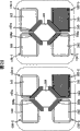
The structure of the solid camera head of first embodiment of the invention is: the gate electrode of the transmission transistor adjacent with the photo-electric conversion element of each pixel extends to form in the mode that covers the photo-electric conversion element top, and peristome is not set on photo-electric conversion element.
Solid camera head, for example, the image element circuit structure example of cmos image sensor is seen Fig. 1.Fig. 1 is the image element circuit of 1 pixel, 1 unit mode.1 pixel 10 comprises photo-electric conversion element 1, comprises the pixel region 8 of transmission transistor 2 and floating empty knot 7, reset transistor 3, address transistor 4, and amplifier transistor 5.
When light was incident in pixel 10,1 pair of incident light of photo-electric conversion element carried out opto-electronic conversion and accumulates signal charge.As the gate electrode input transmission signals RD to transmission transistor 2, then Ji Lei signal charge is transferred to floating empty knot 7 by the raceway groove of transmission transistor 2.In addition, before this transmission,, the current potential of floating empty knot 7 is reset in advance the drain voltage VDD of reset transistor 3 to the gate electrode input reset signal RS of reset transistor 3.By tying 7 transmission signals electric charges from photo-electric conversion element 1 to floating sky, the current potential of floating empty knot 7 changes.Floating empty knot 7 is connected with the gate electrode of amplifier transistor 5, and potential change is modulated the raceway groove of amplifier transistor 5.Next, to the gate electrode Input Address signal AD of address transistor 4.Thus, corresponding with the raceway groove modulation of amplifier transistor 5 signal is output to holding wire 6.So just read the signal corresponding with incident light.After the signal output, floating empty knot 7 is reset to the drain voltage VDD of reset transistor 3.
In Fig. 2, provided an example of the pel array that has disposed pixel 10 two-dimensionally.Under the situation of colour solid camera head, generally constitute 1 unit cell 13 by 4 pixels 10.Fig. 2 has provided the pixel 10 as 4 row, 4 row of an example, the i.e. unit cell 13 of 2 row, 2 row.In each pixel 10, the along continuous straight runs configuration provides the RD line of transmission signals, the AD line that the RS line of reset signal is provided and address signal is provided, and vertically the configuration signal line 6.Constituent parts unit 13 comprises red (R) pixel, green (Gr) pixel, green (Gb) pixel and indigo plant (B) pixel.Incident light is by optionally being limited in the different wave-length coverages with the corresponding filter of each pixel, and the visible light of different wavelength range is incident to each pixel.
Below utilize Fig. 3 and Fig. 4 A, 4B that one example of the unit cell of present embodiment is described.Fig. 3 is the floor map of unit cell one example of present embodiment, and Fig. 4 A, 4B are respectively along the cut-out line A1-A1 shown in Fig. 3, the sectional view of A2-A2.In Fig. 3, for simply only illustrating the pixel region 8 shown in Fig. 1.Unit cell 13 comprises red (R) pixel 100, green (Gr) pixel 110, green (Gb) pixel 120 and blue (B) pixel 130.The transmission transistor 26~29 that each pixel comprises the photo-electric conversion element 14~17 that is arranged in the Semiconductor substrate 30, be adjacent to be provided with photo-electric conversion element 14~17 and be arranged on floating empty knot 22~25 in the Semiconductor substrate 30.Floating empty knot 22~25 is electrically connected to photo-electric conversion element 14~17 by transmission transistor 26~29.14~17 pairs of incident lights of photo-electric conversion element carry out opto-electronic conversion and accumulate signal charge.Transmission transistor 26~29 controls are from the signal charge transmission of photo-electric conversion element 14~17 to floating empty knot 22~25.The gate electrode 18~21 of transmission transistor extends setting in the mode that covers photo-electric conversion element 14~17 above Semiconductor substrate 30.These are different with existing dot structure.In addition, gate electrode 18~21 ground that cover transmission transistor form dielectric film 31, imbed metal line 32 in the dielectric film 31 above transmission transistor 26~29.In addition, on dielectric film 31, lenticule 35~38 is set in the position corresponding with each photo-electric conversion element 14~17.
Require incident light fully to see through to transmission transistor gate electrode 18~21 and be easier to manufacturing etc. with the solid camera head ratio.Consider the absorption of the visible light in the electrode, the conductive material that sees through visible light as electrode material can use for example silicon (Si) or the carborundum (SiC) bigger than Si energy gap.
The absorption of the thick more light of the thickness of gate electrode is big more, and is therefore preferably thin as far as possible.Yet, if thin excessively, for example can on gate electrode, produce pin hole, perhaps when forming contact on the gate electrode, contact through hole can connect gate electrode.When using Si, the gate electrode thickness that the problems referred to above do not take place is for example 50nm.
As described above, in the present embodiment, extend setting in the mode that covers the photo-electric conversion element top, can prevent the incident diffraction of light by transmission transistor gate electrode with each pixel.The solid camera head that can suppress in the Semiconductor substrate the optical crosstalk of the active element adjacent with each pixel can be provided in view of the above.
Variation 1
In the above-described first embodiment, owing in all pixels of R pixel, Gr pixel, Gb pixel, B pixel, the transmission transistor gate electrode is set, the absorption loss water that the light that the transmission transistor gate electrode causes takes place is arranged and the anxiety that makes the photosensitivity reduction in the mode that covers photo-electric conversion element.Especially, with the corresponding pixel of visible light, particularly B pixel in the relatively large short wavelength zone of the absorption coefficient in gate electrode in, have the absorption loss water of light to become big anxiety.
Variation 1 is for to the transmission transistor gate electrode attenuate of the B pixel of first execution mode mode than the thin thickness of the transmission transistor gate electrode of other pixels.In view of the above, can suppress the absorption loss water of the light at B pixel place.
Below utilize Fig. 5, Fig. 6 A, 6B that the solid camera head of this variation is described.Fig. 5 is the floor map of an example of the unit cell of this variation, and Fig. 6 A, 6B are respectively along the sectional view that cuts off line B1-B1, B2-B2 among Fig. 5.Fig. 5,6A, 6B and Fig. 3,4A, 4B are same formation, comprise R pixel 100, Gr pixel 110, Gb pixel 120 and B pixel 132.
As shown in Figure 6A, other the transmission transistor gate electrode 18~20 of R pixel 100, Gr pixel 110, Gb pixel 120 of the Film Thickness Ratio of the transmission transistor gate electrode 21b of the B pixel 132 of this variation is thin.When incident light 39~42 is incident to each pixel, because the thickness attenuate of the transmission transistor gate electrode 21b of the photo-electric conversion element 17 of covering B pixel 132, so can reduce the absorption of incident light loss of B pixel place.
Consider the absorption of the light in the gate electrode, the thickness that covers the transmission transistor gate electrode 21b of B pixel 132 can be set for example to make through the essentially identical mode of luminous intensity.The light wavelength that is incident to each R pixel, Gr pixel, Gb pixel, B pixel changes according to the filter that uses, the centre wavelength that is incident to the incident light of R pixel is for example 600nm, Gr pixel and Gb pixel place are for example 500nm to 550nm, and B pixel place is for example 450nm.
According to H.Melcior (" Demodulation and PhotodetectionTechniques ", in F.T.Arecchi and E.O.Schulz-Dubois, Eds., LaserHandbook, Vol.1, North-Holland, Amsterdam, 1972, pp.725-835) light transmittance of the light of the 450nm wavelength obtained of the absorption coefficient of the light from silicon is lower than the light transmittance of the light of 600nm wavelength.Therefore, when the gate electrode thickness of R pixel during for the 200nm left and right sides for example, the gate electrode thickness of B pixel can be set at for example 50nm, thus can make both light light transmittance about equally.
In addition, owing in the incident light optically focused zone on Semiconductor substrate 30 surfaces, do not have opening portion, can avoid the generation of the diffraction of the incident light 39~42 that causes because of transmission transistor gate electrode 18~21b.
In the above-mentioned variation, only the thickness to the transmission transistor gate electrode that covers the setting of B pixel has carried out filming according to the absorption of light, but can also carry out filming to the transmission transistor gate electrode of covering Gr pixel and Gb pixel according to the absorbing state of separately light.Like this, by adjusting the gate electrode thickness of transmission transistor separately, can be so that the light transmittance of the light in all pixels be equal substantially.
As mentioned above, same with first execution mode in this variation, by extending the transmission transistor gate electrode that each pixel is set, can prevent the generation of incident light diffraction in the mode that covers the photo-electric conversion element top.And then the problem that descends of the photosensitivity of the B pixel in the most alarming short wavelength zone of the absorption loss water of light that can the suppressor electrode.In view of the above, can provide the solid camera head that can suppress in the Semiconductor substrate near the optical crosstalk of the active element each pixel.
Second execution mode
Solid camera head second embodiment of the invention is, by will extending setting in the mode that covers the photo-electric conversion element top except that the transmission transistor gate electrode of the R pixel the B pixel of the cross talk effects minimum of light, Gr pixel, Gb pixel 3 pixels, the device that takes place with the diffraction that prevents incident light.
Below utilize Fig. 7 and Fig. 8 A, 8B that one example of the unit cell of present embodiment is described.Fig. 7 is the floor map of unit cell one example of present embodiment, and Fig. 8 A, 8B are respectively along the cut-out line C1-C1 shown in Fig. 7, the sectional view of C2-C2.In Fig. 7, for simply only illustrating the pixel region 8 shown in Fig. 1.Unit cell comprises R pixel 100, Gr pixel 110, Gb pixel 120 and B pixel 131.The transmission transistor 26~29 that each pixel comprises the photo-electric conversion element 14~17 that is arranged in the Semiconductor substrate 30, be adjacent to be provided with photo-electric conversion element 14~17 and be arranged on floating empty knot 22~25 in the Semiconductor substrate 30.Only the gate electrode 18~20 of the transmission transistor of R pixel 100, Gr pixel 110, Gb pixel 120 covers the top that photo-electric conversion element 14~16 ground are arranged at Semiconductor substrate 30.In this, different with the dot structure of first execution mode shown in Figure 3.
In the present embodiment, dwindle as mentioned above the transmission transistor of B pixel 131 gate electrode 21a, be arranged at and photo-electric conversion element 17 position adjacent in the mode that does not cover photo-electric conversion element 17.Thus, as first execution mode, both avoided in the B pixel 131 in short wavelength zone can preventing the sensitivity decrease of B pixel again because of covering the generation of the incident light absorption loss water that transmission transistor gate electrode 21 that photo-electric conversion element 17 is provided with causes.
When light is incident to the solid camera head of present embodiment, owing to do not have opening portion, can prevent to be incident to the diffraction of the incident light 39~41 of R pixel 100, Gr pixel 110, Gb pixel 120 in the incident light optically focused zone of Semiconductor substrate 30.For the incident light 42 that is incident to B pixel 131,, the possibility that produces diffraction light 46 is arranged owing to there is the opening portion of transmission transistor gate electrode 21a in the incident light optically focused zone of Semiconductor substrate 30.
But the light that is incident to B pixel 131 is the composition of minimal wave length in the visible light, and the absorption in Semiconductor substrate 30 is very big.Therefore, diffraction light is decayed easily in Semiconductor substrate 30 and is difficult to arrive adjacent active element.So crosstalking of B absorption 131 is very little.Thereby in the structure according to the B pixel 131 of present embodiment, transmission transistor gate electrode 21a does not cover photo-electric conversion element, thereby can effectively prevent the optical absorption loss of the B pixel 131 that causes because of transmission transistor gate electrode 21a.
As mentioned above, in the present embodiment by extending the transmission transistor gate electrode of each pixel of setting except the B pixel in the mode that covers the photo-electric conversion element top, can prevent from the same manner to prevent the decline of image quality with first execution mode substantially because of crosstalking that the incident light diffraction takes place.And then the problem that descends of the photosensitivity of the B pixel in the most alarming short wavelength zone of the absorption loss water of light that can the suppressor electrode.In view of the above, can provide the solid camera head that can suppress in the Semiconductor substrate near the optical crosstalk of the active element each pixel.
In the above-described 2nd embodiment, because the transmission transistor gate electrode is arranged on the photo-electric conversion element of R pixel, Gr pixel, Gb pixel, B pixel 3 pixels,, the absorption loss water of the light that generation transmission transistor gate electrode causes in these pixels makes the anxiety of photosensitivity reduction so being arranged.Especially, have bigger in the loss of the visible absorption in short wavelength zone than the absorption loss water of long wavelength's visible light, be that the absorption loss water of light of Gr pixel, the Gb pixel of short wavelength's one side becomes big problem.
With respect to second embodiment, variation 2 be the transmission transistor gate electrode of 3 pixels such as Gr pixel, Gb pixel, B pixel be not provided in a side of extending on the photo-electric conversion element with the photo-electric conversion element position adjacent on, only the transmission transistor gate electrode of R pixel extends on photo-electric conversion element and the solid camera head that forms.In view of the above, can prevent the absorption loss water of the light of Gr pixel, Gb pixel, B pixel.
Below utilize Fig. 9, Figure 10 A, 10B that the solid camera head of this variation is described.Fig. 9 is the floor map of an example of the unit cell of this variation, and Figure 10 A, 10B are respectively along the sectional view that cuts off line D1-D1, D2-D2 among Fig. 9.Fig. 9,10A, 10B and Fig. 7,8A, 8B are same formation, comprise R pixel 100, Gr pixel 111, Gb pixel 121 and B pixel 131.
Shown in Figure 10 A, 10B, the transmission transistor gate electrode 19a~21a of the Gr pixel 111 of this variation, Gb pixel 121, B pixel 131 is arranged at photo-electric conversion element 15~17 position adjacent and does not cover on the photo-electric conversion element 15~17.Only the transmission transistor gate electrode 18 of R pixel 100 forms in the mode of the top of covering photo-electric conversion element 14.
When incident light 39~42 was incident to each pixel, the incident light 39 at R pixel 100 places was owing to there is not opening in the incident light optically focused zone on Semiconductor substrate 30 surfaces and diffraction of light does not take place.Be incident to the incident light 40~42 of Gr pixel 111, Gb pixel 121, B pixel 131 these 3 pixels, there is opening owing to be disposed on the gate electrode 19a~21a of transmission transistor in incident light optically focused zone on Semiconductor substrate 30 surfaces, so produce diffraction light 44~46.
But the incident light that is incident to Gr pixel 111, Gb pixel 121, B pixel 131 these 3 pixels is shorter than the light wavelength that is incident to R pixel 100, and therefore the absorptance in Semiconductor substrate is bigger.So diffraction light 44~46 is decayed easily in Semiconductor substrate 30 and is difficult to arrive adjacent active element.So crosstalking that Gr pixel 111, Gb pixel 121, B pixel 131 cause is very little.Therefore, this variation do not cover structure on the photo-electric conversion element 15~17 of Gr pixel 111, Gb pixel 21, B pixel 131 with the transmission transistor gate electrode, can prevent the absorption loss water of the light that the gate electrode in the photo-electric conversion element 15~17 causes, also become the countermeasure of effectively crosstalking simultaneously.
As mentioned above, this variation can similarly prevent to prevent the reduction of image quality because of crosstalking that the incident diffraction of light produces with second execution mode by only extending the transmission transistor gate electrode that the R pixel is set in the mode that covers the photo-electric conversion element top basically.And then the problem that descends of the photosensitivity of the Gr pixel in the most alarming short wavelength zone of the absorption loss water of light that can the suppressor electrode, Gb pixel, B pixel.In view of the above, can provide the solid camera head that can suppress in the Semiconductor substrate near the optical crosstalk of the active element each pixel.
The 3rd execution mode
So far first and second illustrated execution mode with and variation be the solid camera head of 1 pixel, 1 unit mode, the 3rd execution mode of the present invention is the solid camera head that is suitable for 2 pixels, the 1 unit mode of Highgrade integration
Figure 11 is the example of image element circuit structure of action that is used to illustrate the solid camera head of 2 pixels, 1 unit mode.The difference of the solid camera head of 2 pixels, 1 unit mode and 1 pixel, the 1 unit mode shown in Fig. 1 is, comprises 2 photo-electric conversion element 1-1,1-2 and 2 transmission transistor 2-1,2-2 among the pixel region 8-2, their shared 1 floating empty knots 7.In view of the above, reset transistor 3, address transistor 4 and amplifier transistor 5 each can be cut down, Highgrade integration can be realized for 2 pixels.Basic identical in the action with the situation of 1 pixel, 1 unit mode, but alternately carry out accumulating reading of charge signal in photo-electric conversion element 1-1 and photo-electric conversion element 1-2.
The benefit that shared so floating empty ligament comes is, can cut down the number of transistors of per 1 pixel, increases the aperture opening ratio of photo-electric conversion element, more helps Highgrade integration etc. than 1 pixel, 1 unit mode.
Figure 12 is the example of pixel Butut of the solid camera head of present embodiment.For simply only illustrating the pixel region 8-2 shown in Figure 11.22 pixel cells 71,72 constitute 1 unit cell 73.2 pixel cells 71 comprise 2 pixels, are R pixel 100 and Gb pixel 121; 2 pixel cells 72 comprise other 2 pixels, are Gr pixel 111 and B pixel 131.Provide 4 unit cells among the figure, promptly comprised 16 pel array of 2 pixel cells of 2 row, 4 row.R pixel 100 and Gb pixel 121 shared floating empty knots 69, Gr pixel 111 and B pixel 131 shared floating empty knots 70.At this, utilize each transmission transistor gate electrode to describe, but be not limited thereto with formation example with above-mentioned variation 2 the same manners.Here the transmission transistor gate electrode 65 to R pixel 100 only is provided with in the mode that covers photo-electric conversion element 61, and the transmission transistor gate electrode 66a~68a of Gr pixel 111, Gb pixel 121, B pixel 131 describes with the structure that the mode adjacent with photo-electric conversion element 62~64 is provided with respectively.
Figure 13,14 is the schematic diagram that is used for the cross section structure of pixels illustrated, is respectively along the sectional view that cuts off line E1-E1, E2-E2 among Figure 12.The photo-electric conversion element 61~64 of each R pixel 100, Gr pixel 111, Gb pixel 121, B pixel 131 is arranged in the Semiconductor substrate 74.The transmission transistor gate electrode 65 of R pixel 100 is provided with in the mode that covers photo-electric conversion element 61, and the transmission transistor gate electrode 66a~68a of Gr pixel 111, Gb pixel 121, B pixel 131 is provided with in the mode adjacent with photo-electric conversion element 62~64.Transmission transistor gate electrode 65 and 67a and 66a and 68a will be will float the relatively adjacent setting of empty the knot 69 and 70 mode directions that are clipped in the middle respectively.Floating sky knot 69 and 70 is to be arranged in the Semiconductor substrate 74 by 2 pixels 100 and 121 and 111 and 131 shared modes respectively.
Form the dielectric film 75 of covering Semiconductor substrate 74 and transmission transistor gate electrode 65,66a~68a, metal line 76 is provided with in the mode in the dielectric film 75 of imbedding transmission transistor gate electrode 65,66a~68a top.In addition, lenticule 77~80 is set on dielectric film 75.
Shown in Figure 13,14, when incident light 81~84 is incident to each pixel, because there is not opening in the incident light optically focused zone on Semiconductor substrate 74 surfaces of R pixel 100, can prevent the problem of the diffraction that incident light 81 causes because of the transmission transistor gate electrode 65 of R pixel 100.Because there is opening in the transmission transistor gate electrode 66a~68a place in the incident light optically focused area configurations on Semiconductor substrate 74 surfaces, so be incident to incident light 82~84 generation diffraction lights 86~88 of Gr pixel 111, Gb pixel 121, B pixel 131.But at Gr pixel 111, Gb pixel 121, B pixel 131 places, as illustrated in the above-mentioned variation 2, these diffraction light 86~88 decay in Semiconductor substrate 74 are very big.Therefore, crosstalking of the light in the pixel 111~131 is very little, and present embodiment becomes the countermeasure of effectively crosstalking.
At this, to each transmission transistor gate electrode to be illustrated with the same formation example of above-mentioned variation 2, even but above-mentioned first and second execution mode or the arbitrary structure of variation 1 and variation 2 or to have other structures that the mode of same function therewith designs of each transmission transistor gate electrode also is applicable to present embodiment.
In addition, provided the examples of 2 shared 1 floating empty knots of pixels in the above-mentioned execution mode, still, for example will float in Figure 12 that empty knot 69 is connected with 70,1 floating empty knot by the mode of the shared 4 pixels Unit 1 of 4 pixels 100,111,121,131 also can.
As above illustrated, in solid camera head according to 2 pixels, the 1 unit mode of present embodiment, by only extending the transmission transistor gate electrode that the R pixel is set in the mode that covers the photo-electric conversion element top, can similarly prevent from also can prevent image quality reduction with second execution mode basically because of crosstalking that the incident light diffraction produces.And then face most in the Gr pixel, Gb pixel, B pixel in the short wavelength zone of people's worry in the absorption loss water of the light of gate electrode, because the transmission transistor gate electrode does not form in the mode that covers the photo-electric conversion element top, can prevent the problem of the photosensitivity decline of these pixels.In view of the above, can provide the solid camera head that can suppress in the Semiconductor substrate near the optical crosstalk of the active element of each pixel.
Below utilize Figure 15, Figure 16 that the solid camera head of this variation is described.Figure 15 is the floor map of an example of the unit cell of this variation, and Figure 16 is along the sectional view that cuts off line F2-F2 among Figure 15.
In this variation, as shown in the figure, for example, the transmission transistor gate electrode 65c of R pixel 103-4 with the opposition side to the Gb pixel 121-4 of shared floating empty knot 69 extend, the mode adjacent with the photo-electric conversion element of the Gb pixel 121-2 of adjacent unit cell be provided with.
The effect of this variation and above-mentioned the 3rd execution mode are same, owing to further increased the transmission transistor gate electrode 65c that covers the photo-electric conversion element 61 of R pixel 101, can further reduce the diffraction of the incident light 81 that is incident to R pixel 101 than above-mentioned the 3rd execution mode.By the structure of this variation, for example,, also can effectively suppress the generation of crosstalking even the incident light zone of causing because of oblique incident ray etc. increases.
At this, each transmission transistor gate electrode is illustrated with the same formation example of above-mentioned variation 2, even but above-mentioned first and second execution mode or the arbitrary structure of variation 1 and variation 2 or to have other structures that the mode of same function therewith designs of each transmission transistor gate electrode also is applicable to present embodiment.
The 4th execution mode
The 4th execution mode of the present invention is the solid camera head of 2 pixels, the 1 unit mode of the further Highgrade integration of comparable above-mentioned the 3rd execution mode.Being characterized as of the solid camera head of present embodiment has the inclination gate electrode that is arranged at obliquely on the photo-electric conversion element.In addition, at least one inclination gate electrode extends setting in the mode that covers on the photo-electric conversion element.
Figure 17 is the floor map of an example of the solid camera head of present embodiment.2 unit cells of forming by 4 pixels 105,116,126,136 of 2 row, 2 row have been provided among the figure.1 angle of the photo-electric conversion element 161~164 of each pixel is cut to about 45, cuts part at this and is obliquely installed transmission transistor gate electrode 165,166a~168a.
The floating empty knot 169,170 of middle section configuration between 4 pixels.1 floating empty knot is shared by 2 pixels.In the legend, floating sky knot 169 is shared by R pixel 105 and Gb pixel 126, and floating sky knot 170 is shared by Gr pixel 116 and B pixel 136.The shared method of floating empty knot is not limited to two up and down shown in Figure 17, and is for example, also can be by 2 adjacent pixels of the left and right sides shared or shared by become a partner 2 pixels of linea angulata direction of floating sky.
One side facing to photo-electric conversion element 161~164 of floating empty knot 169,170 forms so that the fixing mode of channel width of inclination gate electrode 165,166a~168a below is parallel to the hypotenuse ground of photo-electric conversion element 161~164.Its result, floating empty knot 169,170 is not simple rectangle but complicated shape.
Usually when transmission transistor is the inclination gate electrode, the pixel that is subjected to the cross talk effects that the incident light by certain pixel causes easily is different with the situation of above-mentioned first to the 3rd execution mode.Owing to crosstalk, the pixel that is disposed at the direction vertical with the gate electrode end of photo-electric conversion element one side is produced crosstalk easily because of incident light generation diffraction phenomena in gate electrode end place produces.For example, when light is incident to the R pixel, inclination B pixel is produced crosstalks, and to about or neighbouring Gr pixel or Gb pixel crosstalk very little.Equally, when light is incident to the Gr pixel, crosstalking to the Gb pixel taken place.
Present embodiment is crosstalked in order to suppress this, extends at least one that transmission transistor gate electrode 165~168 is set in the mode that covers on the corresponding photo-electric conversion element 161~164.In the example of Figure 17, the gate electrode 165 of R pixel 105 is provided with in the mode that covers on the photo-electric conversion element 161.The incident light that is incident to R pixel 105 is longer than the light wavelength that is incident to other pixels 116~136, and therefore the absorption in Semiconductor substrate is little, crosstalks easily.Therefore, transmission transistor gate electrode 165 extensions of R pixel 105 are arranged on the photo-electric conversion element, thereby can prevent the optical diffraction phenomenon at R pixel 105 places, prevent the reduction of image quality.In the present embodiment, the gate electrode of transmission transistor forms in the mode that only extends on the R pixel, but is not limited in this, also can extend on other pixels.
Thus, can provide the solid camera head that can suppress in the Semiconductor substrate near the optical crosstalk of the active element each pixel.
Figure 18 is the floor map according to an example of the solid camera head of variation 4.Unit cell comprises 4 pixels 105,115,125,135.Floating empty knot 169,170 is disposed at the middle section of 4 pixels 105,115,125,135, and is shared by being disposed at become a partner 2 pixels of linea angulata direction of floating sky respectively.That is, floating sky knot 170 is shared by Gr pixel 115 and Gb pixel 125, and floating sky knot 169 is shared by the B pixel 135 of R pixel 105 and adjacent cells unit.
The gate electrode 165~168 of the transmission transistor of each pixel is provided with in the mode that covers on the corresponding photo-electric conversion element 161~164.Can prevent the diffraction of light of gate electrode end in view of the above, provide and suppressed the solid camera head of crosstalking.
When covering photo-electric conversion element because of gate electrode and cause the loss of light to become problem, as described in variation 1, the light absorption of the incident light of each pixel that the thickness by changing each gate electrode causes because of gate electrode with compensation, thus can reduce the loss of each light that absorbs.
Thus, can provide the solid camera head that can suppress in the Semiconductor substrate near the optical crosstalk of the active element each pixel.
The 5th execution mode
The 5th execution mode of the present invention is the solid camera head with 4 pixels, 1 unit mode of inclination gate electrode.In addition, at least one gate electrode in the unit cell is provided with in the mode that covers photo-electric conversion element.
Figure 19 is the example of image element circuit structure of action that is used to illustrate the solid camera head of 4 pixels, 1 unit mode.The difference of the solid camera head of 4 pixels, 1 unit mode and 2 pixels, the 1 unit mode shown in Figure 11 is that pixel region 8-4 comprises 4 photo-electric conversion element 1-1~1-4 and 4 transmission transistor 2-1~2-4, their shared 1 floating empty knots 7.In view of the above, can cut down to each 1 floating empty knot 7, reset transistor 3, address transistor 4 and amplifier transistor 54 pixels.Thus, can increase the interior photo-electric conversion element ratio of occupied area of unit cell, thereby can realize Highgrade integration.Basic identical in the action with the situation of 1 pixel, 1 unit mode, 2 pixels, 1 unit mode, but the charge signal that accumulates among photo-electric conversion element 1-1~1-4 is called over.
Figure 20 is the floor map of an example of the solid camera head of the 5th execution mode.2 unit cells have been provided among the figure by 4 pixels 105,116,126,136 that comprise 2 row, 2 row.Middle section in the constituent parts unit is provided with 1 floating empty knot 169.The photo-electric conversion element 161~164 of each pixel is cut to about 45 near an angle of floating junction 169, cuts part at this and is obliquely installed transmission transistor gate electrode 165,166a~168a.
In this example, also extend the transmission transistor gate electrode 165 that R pixel 105 is set in the mode that covers on the photo-electric conversion element 161.Gate electrode 166a~the 168a of the transmission transistor of other pixels 116~136 and photo-electric conversion element 162~164 are adjacent to be provided with.Gate electrode is not limited to form in the mode that only extends on the R pixel, also can optionally or entirely extend on other pixels as mentioned above.In addition, making each gate electrode by the lambda1-wavelength according to each pixel is suitable thickness, makes the light intensity be incident to each photo-electric conversion element not rely on its wavelength and roughly the same.
As mentioned above, according to various execution modes of the present invention, by with at least one pixel that extends to the mode setting unit unit on the photo-electric conversion element such as the transmission transistor gate electrode of R pixel, then both can prevent the generation of optical diffraction phenomenon, the solid camera head that can suppress in the Semiconductor substrate near the optical crosstalk of the active element each pixel can be provided again.
Industry technical staff is easy to make the into raising and the improvement in a step.Therefore, the present invention is not limited only to detail described herein and exemplary embodiment on wider scope.Thereby, under the prerequisite that does not depart from claims and the purport of the present invention that equivalent limited thereof, can make various changes to it.
Claims (20)
1. solid camera head,
Have a plurality of pixels,
Each pixel comprises:
Be arranged in the Semiconductor substrate, incident light carried out opto-electronic conversion and accumulates the photo-electric conversion element of signal charge;
In above-mentioned Semiconductor substrate, be provided with above-mentioned photo-electric conversion element contiguously, accumulate the floating empty knot of signal charge temporarily; With
The above-mentioned signal charge that accumulates in the above-mentioned photo-electric conversion element is transferred to the above-mentioned floating empty transmission transistor of tying,
Wherein, the above-mentioned transmission transistor of at least one of above-mentioned pixel has in the mode that fully covers above-mentioned photo-electric conversion element top and extends the gate electrode of setting, and remaining transmission transistor of above-mentioned pixel has at least one gate electrode that does not cover above-mentioned photo-electric conversion element.
2. solid camera head as claimed in claim 1 is characterized by:
Above-mentioned remaining transmission transistor in above-mentioned a plurality of pixel has the gate electrode that fully covers above-mentioned photo-electric conversion element top.
3. solid camera head as claimed in claim 1 is characterized by:
Also possess the unit cell that comprises a plurality of pixels that are adjacent to be provided with, the above-mentioned photo-electric conversion element of each pixel in the above-mentioned unit cell receives the incident light that optionally is limited in the different wavelength region may.
4. solid camera head as claimed in claim 3 is characterized by:
The thickness of the above-mentioned gate electrode that is provided with in the mode that covers above-mentioned photo-electric conversion element top is with to be incident to incident light wavelength this photo-electric conversion element, that optionally limited corresponding and different.
5. solid camera head as claimed in claim 3 is characterized by:
The above-mentioned gate electrode that is provided with in the mode that covers above-mentioned photo-electric conversion element top optionally is set up according to the incident light wavelength that is incident in this photo-electric conversion element, has optionally been limited.
6. solid camera head as claimed in claim 3 is characterized by:
The above-mentioned gate electrode that is provided with in the mode that covers above-mentioned photo-electric conversion element top extends to the opposition side of the pixel of shared floating empty knot, with the photo-electric conversion element adjacency of adjacent unit cell.
7. solid camera head as claimed in claim 3 is characterized by:
The above-mentioned transmission transistor of at least one pixel in above-mentioned a plurality of pixel has the gate electrode that does not cover above-mentioned photo-electric conversion element top.
8. solid camera head as claimed in claim 1 is characterized by:
Above-mentioned gate electrode is the conductive material that can see through visible light.
9. solid camera head,
Have a plurality of pixels,
Each pixel comprises:
Be arranged in the Semiconductor substrate, incident light carried out opto-electronic conversion and accumulates the photo-electric conversion element of signal charge;
In above-mentioned Semiconductor substrate, be provided with above-mentioned photo-electric conversion element contiguously, accumulate the floating empty knot of signal charge temporarily; With
The above-mentioned signal charge that accumulates in the above-mentioned photo-electric conversion element is transferred to the above-mentioned floating empty transmission transistor of tying,
Wherein, above-mentioned floating empty knot by via the above-mentioned transmission transistor corresponding with a plurality of above-mentioned photo-electric conversion elements being electrically connected by the shared mode of a plurality of above-mentioned photo-electric conversion elements, and
The above-mentioned transmission transistor of at least one of above-mentioned pixel has the gate electrode that is provided with in the mode that fully covers above-mentioned photo-electric conversion element top, and remaining transmission transistor of above-mentioned pixel has at least one gate electrode that does not cover above-mentioned photo-electric conversion element.
10. solid camera head as claimed in claim 9 is characterized by:
Above-mentioned remaining transmission transistor in above-mentioned a plurality of pixel has the gate electrode that fully covers above-mentioned photo-electric conversion element top.
11. solid camera head as claimed in claim 9 is characterized by:
Also possess the unit cell that comprises a plurality of pixels that are adjacent to be provided with, the above-mentioned photo-electric conversion element of each pixel in the above-mentioned unit cell receives the incident light that optionally is limited in the different wavelength region may.
12. solid camera head as claimed in claim 11 is characterized by:
The thickness of the above-mentioned gate electrode that is provided with in the mode that covers above-mentioned photo-electric conversion element top is with to be incident to incident light wavelength this photo-electric conversion element, that optionally limited corresponding and different.
13. solid camera head as claimed in claim 11 is characterized by:
The above-mentioned gate electrode that is provided with in the mode that covers above-mentioned photo-electric conversion element top optionally is set up according to the incident light wavelength that is incident in this photo-electric conversion element, has optionally been limited.
14. solid camera head as claimed in claim 11 is characterized by:
The above-mentioned gate electrode that is provided with in the mode that covers above-mentioned photo-electric conversion element top extends to the opposition side of the pixel of shared floating empty knot, with the photo-electric conversion element adjacency of adjacent unit cell.
15. solid camera head as claimed in claim 11 is characterized by:
The above-mentioned transmission transistor of at least one pixel in above-mentioned a plurality of pixel has the gate electrode that does not cover above-mentioned photo-electric conversion element top.
16. solid camera head as claimed in claim 9 is characterized by:
Above-mentioned gate electrode is the conductive material that can see through visible light.
17. solid camera head as claimed in claim 9 is characterized by:
1 angle of above-mentioned photo-electric conversion element cuts with being tilted, and above-mentioned transmission transistor has the gate electrode that is obliquely installed on the above-mentioned angle that is cut obliquely of above-mentioned photo-electric conversion element,
Above-mentioned floating empty knot is disposed at 4 middle sections between pixel.
18. solid camera head as claimed in claim 17 is characterized by:
Above-mentioned floating empty knot is shared by the 2 pixels institute adjacent with this floating empty knot.
19. solid camera head as claimed in claim 18 is characterized by:
Above-mentioned 2 pixels along the diagonal of above-mentioned floating empty knot with should be adjacent to configuration by floating empty knot.
20. solid camera head as claimed in claim 14 is characterized by:
Above-mentioned floating empty knot is by shared with above-mentioned floating empty 4 the pixels institutes that are adjacent to dispose of tying.
Applications Claiming Priority (3)
| Application Number | Priority Date | Filing Date | Title |
|---|---|---|---|
| JP2006117046A JP4764243B2 (en) | 2006-04-20 | 2006-04-20 | Solid-state imaging device |
| JP2006-117046 | 2006-04-20 | ||
| JP2006117046 | 2006-04-20 |
Publications (2)
| Publication Number | Publication Date |
|---|---|
| CN101060128A CN101060128A (en) | 2007-10-24 |
| CN101060128B true CN101060128B (en) | 2011-04-20 |
Family
ID=38619106
Family Applications (1)
| Application Number | Title | Priority Date | Filing Date |
|---|---|---|---|
| CN2007101012716A Expired - Fee Related CN101060128B (en) | 2006-04-20 | 2007-04-20 | Solid-state imaging device |
Country Status (4)
| Country | Link |
|---|---|
| US (1) | US7719591B2 (en) |
| JP (1) | JP4764243B2 (en) |
| KR (1) | KR100884860B1 (en) |
| CN (1) | CN101060128B (en) |
Families Citing this family (14)
| Publication number | Priority date | Publication date | Assignee | Title |
|---|---|---|---|---|
| JP2009059811A (en) * | 2007-08-30 | 2009-03-19 | Sharp Corp | Solid-state image pick-up apparatus, and electronic information appliance |
| US20090091264A1 (en) * | 2007-10-04 | 2009-04-09 | Himax Technologies Limited | Pixel circuit |
| JP5181840B2 (en) * | 2008-05-30 | 2013-04-10 | ソニー株式会社 | Solid-state imaging device, driving method of solid-state imaging device, and electronic apparatus |
| US8035716B2 (en) * | 2008-06-13 | 2011-10-11 | Omnivision Technologies, Inc. | Wide aperture image sensor pixel |
| JP2010016056A (en) * | 2008-07-01 | 2010-01-21 | Canon Inc | Photoelectric conversion device |
| US20100002115A1 (en) * | 2008-07-03 | 2010-01-07 | Xinqiao Liu | Method for Fabricating Large Photo-Diode Arrays |
| JP5476832B2 (en) * | 2009-07-23 | 2014-04-23 | ソニー株式会社 | Solid-state imaging device and camera |
| JP5132640B2 (en) * | 2009-08-25 | 2013-01-30 | 株式会社東芝 | Solid-state imaging device and manufacturing method thereof |
| JP5564874B2 (en) * | 2009-09-25 | 2014-08-06 | ソニー株式会社 | Solid-state imaging device and electronic apparatus |
| JP5569156B2 (en) | 2010-06-07 | 2014-08-13 | ソニー株式会社 | Image display device, electronic device, image display system, image acquisition method, program |
| JP2015065270A (en) * | 2013-09-25 | 2015-04-09 | ソニー株式会社 | Solid state image pickup device and manufacturing method of the same, and electronic apparatus |
| KR102513483B1 (en) * | 2017-11-30 | 2023-03-24 | 에스케이하이닉스 주식회사 | Image sensor and method of fabricating the same |
| CN110112153A (en) * | 2019-04-11 | 2019-08-09 | 天津大学 | A kind of TOF imaging sensor demodulation pixel structure of charge fast transfer |
| US11393866B2 (en) * | 2019-09-30 | 2022-07-19 | Taiwan Semiconductor Manufacturing Company, Ltd. | Method for forming an image sensor |
Citations (1)
| Publication number | Priority date | Publication date | Assignee | Title |
|---|---|---|---|---|
| US4242694A (en) * | 1976-09-13 | 1980-12-30 | Hitachi, Ltd. | Solid-state color imaging device |
Family Cites Families (18)
| Publication number | Priority date | Publication date | Assignee | Title |
|---|---|---|---|---|
| JPH05335549A (en) * | 1992-06-01 | 1993-12-17 | Matsushita Electric Ind Co Ltd | Solid state image sensor and driving method therefor |
| JPH06151797A (en) * | 1992-11-11 | 1994-05-31 | Sony Corp | Solid-state image sensing element |
| KR0186183B1 (en) * | 1995-12-19 | 1999-03-20 | 문정환 | Color solid state imaging device |
| KR100550020B1 (en) | 1997-03-12 | 2006-10-31 | 세이코 엡슨 가부시키가이샤 | Pixel circuits, displays and electronics equipped with current-driven light emitting devices |
| JP3442283B2 (en) | 1998-04-28 | 2003-09-02 | セイコーインスツルメンツ株式会社 | Linear image sensor |
| FR2781929B1 (en) * | 1998-07-28 | 2002-08-30 | St Microelectronics Sa | IMAGE SENSOR WITH PHOTODIODE ARRAY |
| US6624850B1 (en) | 1998-12-30 | 2003-09-23 | Eastman Kodak Company | Photogate active pixel sensor with high fill factor and correlated double sampling |
| JP2001339056A (en) * | 2000-05-26 | 2001-12-07 | Canon Inc | Solid-state camera |
| US7154546B1 (en) * | 2000-08-07 | 2006-12-26 | Micron Technology, Inc. | Pixel optimization for color |
| JP2004014911A (en) * | 2002-06-10 | 2004-01-15 | Renesas Technology Corp | Semiconductor device and its manufacturing method |
| KR20040036087A (en) * | 2002-10-23 | 2004-04-30 | 주식회사 하이닉스반도체 | CMOS image sensor having different depth of photodiode by Wavelength of light |
| JP2004228425A (en) * | 2003-01-24 | 2004-08-12 | Renesas Technology Corp | Manufacturing method of cmos image sensor |
| CN100449764C (en) * | 2003-11-18 | 2009-01-07 | 松下电器产业株式会社 | Photodetector |
| JP4071190B2 (en) | 2003-12-02 | 2008-04-02 | シャープ株式会社 | Amplification type solid-state imaging device and driving method thereof |
| JP2005129965A (en) * | 2004-11-29 | 2005-05-19 | Toshiba Corp | Solid-state imaging device |
| KR100642753B1 (en) * | 2005-02-11 | 2006-11-10 | 삼성전자주식회사 | image sensor |
| US7534982B2 (en) * | 2005-06-09 | 2009-05-19 | Micron Technology, Inc. | Reduced imager crosstalk and pixel noise using extended buried contacts |
| JP4752447B2 (en) * | 2005-10-21 | 2011-08-17 | ソニー株式会社 | Solid-state imaging device and camera |
-
2006
- 2006-04-20 JP JP2006117046A patent/JP4764243B2/en not_active Expired - Fee Related
-
2007
- 2007-04-17 US US11/736,315 patent/US7719591B2/en not_active Expired - Fee Related
- 2007-04-19 KR KR1020070038439A patent/KR100884860B1/en not_active IP Right Cessation
- 2007-04-20 CN CN2007101012716A patent/CN101060128B/en not_active Expired - Fee Related
Patent Citations (1)
| Publication number | Priority date | Publication date | Assignee | Title |
|---|---|---|---|---|
| US4242694A (en) * | 1976-09-13 | 1980-12-30 | Hitachi, Ltd. | Solid-state color imaging device |
Also Published As
| Publication number | Publication date |
|---|---|
| JP2007294486A (en) | 2007-11-08 |
| KR20070104263A (en) | 2007-10-25 |
| US7719591B2 (en) | 2010-05-18 |
| CN101060128A (en) | 2007-10-24 |
| US20070247537A1 (en) | 2007-10-25 |
| JP4764243B2 (en) | 2011-08-31 |
| KR100884860B1 (en) | 2009-02-23 |
Similar Documents
| Publication | Publication Date | Title |
|---|---|---|
| CN101060128B (en) | Solid-state imaging device | |
| US7741689B2 (en) | Photoelectric conversion layer-stacked solid-state imaging element | |
| US6632702B2 (en) | Color image sensor and method for fabricating the same | |
| US8159010B2 (en) | Solid-state image pick-up device and imaging system using the same | |
| WO2015037547A1 (en) | Solid-state imaging device | |
| JP5219348B2 (en) | Image sensor including active pixel sensor array | |
| US20220085220A1 (en) | Image sensor and image-capturing device | |
| US7208811B2 (en) | Photo-detecting device | |
| KR100477911B1 (en) | Solid-state image pickup device, method of manufacturing same and camera | |
| KR101426951B1 (en) | Solid-state imaging device and electronic device | |
| US20200395397A1 (en) | Image sensor and image-capturing device | |
| KR20060104936A (en) | Solid-state image pick-up device | |
| JP4751576B2 (en) | Photoelectric conversion film stack type solid-state imaging device | |
| JPH06204450A (en) | Solid-state image pickup device | |
| JP2008153370A (en) | Solid-state imaging device and its manufacturing method | |
| JPH05175471A (en) | Solid-state image sensing device | |
| US20100187582A1 (en) | Solid-state imaging device having transmission gates which pass over part of photo diodes when seen from the thickness direction of the semiconductor substrate | |
| JP2521789B2 (en) | Photosensitive unit structure of solid-state imaging device | |
| KR20070076611A (en) | Image sensor for reducing current leakage | |
| JPS59196667A (en) | Solid-state image pickup device | |
| JPS5870685A (en) | Solid-state image pickup device | |
| JPH10209424A (en) | Solid-state imaging element | |
| JPH11330447A (en) | Solid-state image-pickup element | |
| JPH0794701A (en) | Solid state image sensing device | |
| JP2006032771A (en) | Solid-state imaging device |
Legal Events
| Date | Code | Title | Description |
|---|---|---|---|
| C06 | Publication | ||
| PB01 | Publication | ||
| C10 | Entry into substantive examination | ||
| SE01 | Entry into force of request for substantive examination | ||
| C14 | Grant of patent or utility model | ||
| GR01 | Patent grant | ||
| CF01 | Termination of patent right due to non-payment of annual fee |
Granted publication date: 20110420 Termination date: 20170420 |
|
| CF01 | Termination of patent right due to non-payment of annual fee |