CN101038531A - Shared interface for cmponents in an embedded system - Google Patents
Shared interface for cmponents in an embedded system Download PDFInfo
- Publication number
- CN101038531A CN101038531A CNA2007101035012A CN200710103501A CN101038531A CN 101038531 A CN101038531 A CN 101038531A CN A2007101035012 A CNA2007101035012 A CN A2007101035012A CN 200710103501 A CN200710103501 A CN 200710103501A CN 101038531 A CN101038531 A CN 101038531A
- Authority
- CN
- China
- Prior art keywords
- nonvolatile memory
- volatile memory
- shared
- interface
- memory controller
- Prior art date
- Legal status (The legal status is an assumption and is not a legal conclusion. Google has not performed a legal analysis and makes no representation as to the accuracy of the status listed.)
- Pending
Links
Images


Classifications
-
- G—PHYSICS
- G06—COMPUTING; CALCULATING OR COUNTING
- G06F—ELECTRIC DIGITAL DATA PROCESSING
- G06F13/00—Interconnection of, or transfer of information or other signals between, memories, input/output devices or central processing units
- G06F13/14—Handling requests for interconnection or transfer
- G06F13/16—Handling requests for interconnection or transfer for access to memory bus
- G06F13/1668—Details of memory controller
- G06F13/1694—Configuration of memory controller to different memory types
-
- G—PHYSICS
- G11—INFORMATION STORAGE
- G11C—STATIC STORES
- G11C16/00—Erasable programmable read-only memories
-
- Y—GENERAL TAGGING OF NEW TECHNOLOGICAL DEVELOPMENTS; GENERAL TAGGING OF CROSS-SECTIONAL TECHNOLOGIES SPANNING OVER SEVERAL SECTIONS OF THE IPC; TECHNICAL SUBJECTS COVERED BY FORMER USPC CROSS-REFERENCE ART COLLECTIONS [XRACs] AND DIGESTS
- Y02—TECHNOLOGIES OR APPLICATIONS FOR MITIGATION OR ADAPTATION AGAINST CLIMATE CHANGE
- Y02D—CLIMATE CHANGE MITIGATION TECHNOLOGIES IN INFORMATION AND COMMUNICATION TECHNOLOGIES [ICT], I.E. INFORMATION AND COMMUNICATION TECHNOLOGIES AIMING AT THE REDUCTION OF THEIR OWN ENERGY USE
- Y02D10/00—Energy efficient computing, e.g. low power processors, power management or thermal management
Landscapes
- Engineering & Computer Science (AREA)
- Theoretical Computer Science (AREA)
- Physics & Mathematics (AREA)
- General Engineering & Computer Science (AREA)
- General Physics & Mathematics (AREA)
- Multi Processors (AREA)
- Memory System (AREA)
- Storage Device Security (AREA)
Abstract
Embodiments of the invention provide a method and apparatus for accessing a non-volatile memory controller and a volatile memory via a shared interface. In one embodiment, the method includes selecting one of the non-volatile memory controller and the volatile memory via shared control signals of the shared interface, wherein the shared control signals are issued to the non-volatile memory controller and the volatile memory. The method also includes issuing commands to the selected one of the non-volatile memory controller and the volatile memory via the shared control signals.
Description
Technical field
The present invention relates generally to a kind of computer system.Especially, the present invention relates to system and method after a kind of improvement that is used for the computer system interface unit.
Background technology
Many modern electronic equipments for example cell phone, PDA, portable music player, application apparatus etc. typically combine embedded computer system.Embedded computer system typically comprises the volatile memory of computer processor (being called main frame), nonvolatile memory (for example nand flash memory and/or ROM storer) and for example dynamic RAM (DRAM).Main frame can comprise central processing unit (CPU), digital signal processor (DSP), micro controller unit (MCU) or direct memory access (DMA) (DMA) data transmission device.
In some cases, can provide nonvolatile memory controller (for example, nand flash memory controller) to be used to visit nonvolatile memory.By the nonvolatile memory controller is provided, the control of nonvolatile memory and management role are offloaded from a host to the nonvolatile memory controller, have therefore simplified the design of main frame and other processing demands of permission host process embedded system.
Wherein main frame, nonvolatile memory controller, nonvolatile memory and volatile memory all provide in embedded computer system, and each parts can have one or more interfaces that are used for being connected to system's miscellaneous part.Also realize a kind of like this embedded system for reducing design cost, and, just need when keeping high-caliber performance, reduce the pin count of interface in order to reduce a kind of like this energy consumption of embedded system.
Therefore, just need a kind of improvement system and method that is used for interface in main frame, nonvolatile memory and the volatile memory of embedded computer system.
Summary of the invention
Embodiments of the invention provide a kind of method and apparatus by shared interface visit nonvolatile memory controller and volatile memory.In one embodiment, the method comprises by the shared control signals of shared interface selects in nonvolatile memory controller and the volatile memory one, and wherein shared control signals is published to nonvolatile memory controller and volatile memory.This method also comprises by shared control signals issuing command in selected nonvolatile memory controller and the volatile memory.
Description of drawings
Therefore under the mode that above-mentioned feature of the present invention can specifically be understood, by the above-mentioned feature of reference example short summary, just can obtain more detailed description of the present invention, some of them are described shown in the drawings.Yet, it should be noted that these accompanying drawings only show the exemplary embodiments of this invention, so these accompanying drawings can not think the restriction of the scope of the invention, the present invention can allow other equivalent embodiment.
Fig. 1 shows the block diagram of example system according to an embodiment of the invention.
Fig. 2 A-C shows the operator scheme of system according to an embodiment of the invention.
Fig. 3 shows the shared interface that is used for embedded system according to an embodiment of the invention.
Fig. 4 shows the process flow diagram that uses the method for host access storer according to one embodiment of present invention by shared interface.
Fig. 5 shows the process flow diagram that uses the method for nonvolatile memory controller access volatile memory according to one embodiment of present invention by shared interface.
Fig. 6 shows according to one embodiment of present invention and by shared interface volatile memory is carried out the block diagram of the hardware of visit simultaneously.
Embodiment
Embodiments of the invention generally provide a kind of method and apparatus by shared interface visit nonvolatile memory controller and volatile memory.In one embodiment, this method comprises by the shared control signals of shared interface selects in nonvolatile memory controller and the volatile memory one, and wherein shared control signals is published to nonvolatile memory controller and volatile memory.This method also comprises by shared control signals issuing command in selected nonvolatile memory controller and the volatile memory.In some cases, by the shared control signal that is published to nonvolatile memory controller and volatile memory, can reduce the quantity with the lead-in wire of nonvolatile memory controller and volatile memory interfaces, therefore reduce the complicacy and the energy consumption of system.
Embodiments of the invention about the embedded system that comprises host-processor, volatile memory and nonvolatile memory are described below.Yet in some cases, this embedded system can comprise a plurality of host-processors, a plurality of volatile memory and/or a plurality of nonvolatile memory.Volatile memory can comprise DRAM, the SRAM of any kind or the volatile memory of any other type, and nonvolatile memory can comprise the nonvolatile memory of nand flash memory, NOR flash memory, programmable read-only memory (prom), Electrically Erasable Read Only Memory (EE-PROM), ROM (read-only memory) (ROM) or any other type.Host-processor can comprise the processor of any kind, comprises CPU (central processing unit) (CPU), digital signal processor (DSP), micro controller unit (MCU) or direct memory access (DMA) (DMA) data transmission device.And in some cases, each chip in the system comprises the processor and/or the storer of a plurality of types.For example, main frame can comprise CPU, DSP and SRAM.In some cases, nonvolatile memory can comprise ROM and flash memory.Is conspicuous in conjunction with operable other the exemplary combinations of embodiments of the invention for those of ordinary skills.
Exemplary embedded system
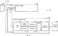
Fig. 1 shows the block diagram of example system 100 according to an embodiment of the invention.As mentioned above, this system 100 (for example can comprise main frame 102, volatile memory 104, the volatile memory of DRAM, SDRAM, DDR-SDRAM, LP-SDRAM and/or any other type), nonvolatile memory controller 106 and nonvolatile memory 108 (for example, the nonvolatile memory of ROM, PROM, EE-PROM, nand flash memory, NOR flash memory and/or any other type).In some cases, the nonvolatile memory controller can comprise guidance code impact damper 120, NAND manager circuit 122, DRAM interface 124, controller code 126, controller kernel 128, dma circuit 130 and non-volatile memory interface 132.
In one embodiment, nonvolatile memory controller 106 can use non-volatile memory interface 132 to visit the information that is stored in the nonvolatile memory 108, and these information comprise guidance code, controller code, behaviour's system code, application code, data and any other information.Similarly, nonvolatile memory controller 106 can use DRAM interface 124 visit volatile memory 104.As described below, the information in the nonvolatile memory 108 can be loaded into guidance code impact damper 120, controller code impact damper 126 and/or volatile memory 104 and be used for the initialization of system 100.For example, be stored in controller code in the controller code impact damper 126 by operation, controller kernel 128 can be used for the implementation controller operation.And as described below, dma circuit 130 can be used for from nonvolatile memory 108 automatic transmission information to volatile memory 104.
In one embodiment of the invention, main frame 102 can use shared interface 140 to visit nonvolatile memory 108 (for example, by nonvolatile memory controller 106) and volatile memory 104.As described, the part of shared interface 140 can be included in the synchronous serial connection (for example, quick connection, DQ/DQS 110) of volatile memory 104.Shared interface 140 also can comprise and is used to provide control signal and address bit shared address and control line (ADR/CTL 112) to volatile memory 104 and/or nonvolatile memory controller 106.And other interfaces of describing in detail more below also can be provided in connect.In some cases, by being provided for visiting the shared interface 140 of nonvolatile memory controller 106 and volatile memory 104, do not need extra lead-in wire that main frame 102 is connected to nonvolatile memory controller 106.For example, be connected to the address of nonvolatile memory controller 106 and each of control lead-in wire and also can be connected to volatile memory 104.
Use the operator scheme of shared interface
In one embodiment of the invention, shared interface 140 can be used for a middle execute store visit in a plurality of patterns.Fig. 2 A-C has described the operator scheme of system 100 according to an embodiment of the invention.
Fig. 2 A shows according to one embodiment of present invention, the block diagram of first pattern of the operation of main frame 102 visit volatile memory 104.As described, main frame 102 can read or be written to the volatile memory from volatile memory by shared interface 140.Under the situation of main frame 102 visit volatile memory 104, main frame 102 can confirm to indicate main frame 102 signal as supvr (for example, interface 140 starts and controls a given side of communicating by letter) on shared interface 140.By confirm indication main frame 102 on interface 140 as gerentocratic signal, other parts (for example, the nonvolatile memory controller 106) that are connected on the shared interface 140 cannot be attempted control interface 140 simultaneously.For example, main frame 102 can utilize shared address and control signal 112 to select volatile memory 104, and issuing command is to volatile memory 104, and the address in the selection volatile memory 104.In one embodiment, main frame 102 can utilize synchronous serial port (or quick port) to transmit data to volatile memory 104 and reading of data from volatile memory 104.The exemplary signal of using in first pattern will more specifically describe below.
Fig. 2 B shows according to one embodiment of present invention, the block diagram of the second mode of operation of main frame 102 visit nonvolatile memories 108.Under the situation of main frame 102 visit nonvolatile memories 108, main frame 102 can confirm to indicate main frame 102 on shared interface 140 as gerentocratic signal.And main frame 102 can utilize shared address and control signal 112 to select nonvolatile memory controller 106, and issuing command is to nonvolatile memory controller 106, and the address in the selection nonvolatile memory 108.In response to instruction and domain addresses that main frame 102 provides by shared interface 140, nonvolatile memory controller 106 can be visited the address in the nonvolatile memory 108, for example, and by non-volatile memory interface 132.In one embodiment, main frame 102 can utilize asynchronous parallel port Data transmission between main frame 102 and nonvolatile memory controller 106, comprises the data that are written to the data in the nonvolatile memory 108 or read from nonvolatile memory 108 by nonvolatile memory controller 106.The exemplary signal of using in second pattern will more specifically describe below.
Fig. 2 C shows according to one embodiment of present invention, the block diagram of the three-mode of the operation of nonvolatile memory controller 106 visit volatile memory 104.Under the situation of nonvolatile memory controller 106 visit volatile memory 104, nonvolatile memory controller 106 can confirm on shared interface 140 that indication nonvolatile memory controller 106 is as the gerentocratic signal of shared interface 140 (for example, thereby prevent that main frame 102 from using interface 140 simultaneously).Nonvolatile memory controller 106 can utilize shared address and control signal 112 to select volatile memory 104 then, and issuing command is to volatile memory 104, and the address in the selection volatile memory 104.In one embodiment, nonvolatile memory controller 106 can utilize asynchronous parallel port Data transmission between nonvolatile memory controller 106 and volatile memory 104.
In one embodiment, the nonvolatile memory controller can transmit data between nonvolatile memory 108 and volatile memory 104.For example, when data are transferred to from nonvolatile memory 108 under the situation of volatile memory 104, nonvolatile memory controller 106 can utilize non-volatile memory interface 132 from nonvolatile memory 108 reading of data.The data that read from nonvolatile memory 108 can be written to volatile memory 104 from nonvolatile memory controller 106 by shared interface 140 then.Can be simply by shared interface 140 and nonvolatile memory controller 106 from volatile memory 104 reading of data and be written to nonvolatile memory 106.In some cases, nonvolatile memory controller 106 can be used for carrying out direct memory access (DMA) (DMA) transmission between nonvolatile memory 108 and volatile memory 104.The exemplary signal of using in three-mode also will more specifically describe below.
Exemplary shared interface
Fig. 3 shows the shared interface 140 that is used for embedded system 100 according to one embodiment of present invention.As described, interface 140 can comprise that shared address is with control 112 and be used for synchronous serial and be connected 110 connection.As described, interface 140 can be connected to main frame 102 or nonvolatile memory controller 106.
In one embodiment, the signal that is used for synchronous serial connection 110 can comprise chip select signal (CS#, " # " expression signal can be effective for hanging down), clock signal (CLK), reverse clock signal (CLK#), clock enable signal (CKE), data mask signal (DM), serial data signal (DQ) and serial data gating signal (DQS).
By nonvolatile memory controller 106, shared address and control signal 112 can comprise that the volatile memory that is used to visit volatile memory 104 is connected 320 and is connected 322 with the nonvolatile memory controller that is used to visit nonvolatile memory 108.In one embodiment, volatile memory connects 320 and can comprise and write enable signal (WE#), column address gating signal (CAS#), rwo address strobe signals (RAS#), address bus (A[15:0]) and memory bank (bank) address bit (BA[1], BA[0]).
As described, volatile memory connection 320 also can be connected to nonvolatile memory connection 322.Respectively, WE# connect can nonvolatile memory connect 320 and the volatile memory controller shared between connecting 322, CAS# connects can be connected 322 address latch signal (ALE) shared with being used for the nonvolatile memory controller, the RAS# signal can be used for the nonvolatile memory controller be connected 322 to read enable signal (RE#) shared, address bit A[15:0] can be used for the nonvolatile memory controller and be connected 322 multiplexed I/O lead-in wire IO[15:0] shared, BA[1] can be connected 322 chip enable signal CE# shared with being used for the nonvolatile memory controller, and BA[0] can be connected 322 manager accesses signal (MA#) shared with being used for the nonvolatile memory controller.Corresponding shared connection (having exemplary main frame lead-in wire numbering) also is shown in the following Table 1.
Table 1: shared interface connects
| The main frame lead-in wire | Volatile memory | The | |
| 0 | ?WE | WE# | |
| 1 | ? | ALE | |
| 2 | ?RAS# | RE# | |
| 3:19 | ?A[15:0] | IO[15:0] | |
| 20 | ?BA[1] | CE# | |
| 21 | ?BA[0] | MA# |
In one embodiment of the invention, being used for the chip enable signal (CE#) 306 of nonvolatile memory controller 106 can be logically derive from the chip enable signal CE# and the chip select signal CS# of shared interface 140.By deriving chip enable signal CE# 306 from CE# and CS# signal, nonvolatile memory controller 106 can determine whether main frame 102 selects nonvolatile memory controller 106 or volatile memory 104.In some cases, if the CE# 306 signal can not be derived from CE# and CS# signal, even do not have chosenly when nonvolatile memory controller 106, nonvolatile memory controller 106 also may react to shared address and control signal 112.For example, when being reduced to low logic level and working as chip select signal CS#, chip enable signal CE# rises to high logic level (thereby cancellation selecting) to volatile memory 104, so just can select nonvolatile memory controller 104 (for example, chip enable signal CE# 306 can reduce).
Select circuit can comprise the NOT door 302 of anti-phase CS# signal and the OR door 304 that CE# signal and anti-phase CS# signal are carried out the logical OR computing.The output of OR door 304 can be connected to CE# signal 306.In one embodiment, this circuit can provide with the form of the separation circuit of relative main frame 102, volatile memory 104 or nonvolatile memory controller 106.Alternatively, main frame 102 or nonvolatile memory controller 106 can produce CE# signal 306, utilize the essential signal that inputs or outputs on the additional feedthrough of the chip that produces signal 306.The selection that is used for the transmission mode of shared interface will more specifically describe below with reference to figure 4-5.
Select operating mode in shared interface
In one embodiment of the invention, main frame 102 and nonvolatile memory controller 106 can use CS#, the CE# of shared interface 140 and supvr that the MA# signal comes option interface 140 and select by shared interface 140 which chip of control.
Fig. 4 shows the process flow diagram that uses the process 400 of main frame 102 reference-to storage according to one embodiment of present invention by shared interface 140.As described, next process 400 can and arrive the step 404 of asking reference-to storage (for example, volatile memory 104 or nonvolatile memory 108) in step 402 beginning.For example, can receive such request from extra equipment or the result who executes instruction as main frame 102.
When the request of receiving, make in step 406 whether main frame 102 is the gerentocratic decision of shared interface 140.For example, make decision by checking by the MA# position of nonvolatile memory controller 106 outputs.If the MA# potential drop is low, nonvolatile memory controller 106 can be that the supvr of shared interface 140 and main frame 102 can be waited for up to the MA# position being raise by nonvolatile memory controller 106 in step 408 so, thereby indication nonvolatile memory controller 106 no longer is the supvr of shared interface 140.
In case main frame 102 becomes the supvr of shared interface 140, make the decision whether visit points to volatile memory 104 in step 410.If made the decision of request of access sensing volatile memory 104, main frame can be confirmed CE# and reduce CS# in step 420 so.By confirming CE#, can be by main frame 102 cancellations selecting to nonvolatile memory controller 106.By reducing CS#, can be by main frame 102 selected volatile memory 104.So, in step 422, main frame 102 can be issued access instruction to volatile memory 104, for example, and by the shared address and the control signal 112 of shared interface 140.So, in step 424, can carry out data access by a port (for example, being used for the connection 110 of synchronous serial port) of volatile memory 104.
If made the decision of request of access sensing nonvolatile memory 108, main frame can reduce CE# and confirm CS# in step 412 so.By reducing CE#, can be by main frame 102 selected nonvolatile memory controllers 106.By confirming CS#, can be by main frame 102 cancellations selecting to volatile memory 104.So, in step 414, main frame 102 can be issued access instruction to nonvolatile memory controller 106, for example, and by the shared address and the control signal 112 of shared interface 140.So, in step 416, can carry out data access by a port (for example, being used for the nonvolatile memory controller connection 322 of asynchronous parallel port) of nonvolatile memory controller 106.Then, process 400 finishes in step 430.
In some cases, nonvolatile memory controller 106 can become the supvr of shared interface 140 and carry out data access between nonvolatile memory 108 and volatile memory 104.For example, nonvolatile memory controller 106 can use shared interface 140 from volatile memory 104 reading of data and use non-volatile memory interface 132 that these data are written to nonvolatile memory 108 then.Nonvolatile memory controller 106 also can use non-volatile memory interface 132 from nonvolatile memory 108 reading of data and by shared interface 140 these data are written to the volatile memory 104 then.In some cases, nonvolatile memory controller 106 can be carried out the DMA transmission between nonvolatile memory 108 and volatile memory 104.
Fig. 5 shows the process flow diagram that uses the process 500 of nonvolatile memory controller 106 visit volatile memory 104 according to one embodiment of present invention by shared interface 140.Process is in step 502 beginning and then to the step 504 that receives the request of carrying out transmission (for example, the data between nonvolatile memory 108 and volatile memory 104).In step 506, if nonvolatile memory controller 106 can be checked CS# and CS# and be high logic level then (for example reduce the MA# signal, mean that main frame 102 does not use shared bus), thus indication nonvolatile memory controller 106 becomes the supvr of shared interface 140.After nonvolatile memory controller 106 becomes the supvr of shared interface 140, nonvolatile memory controller 106 can use shared interface 140 to carry out the transmission of arriving volatile memory 104 from nonvolatile memory 108 (for example, using non-volatile memory interface 132).For example, the asynchronous parallel port that nonvolatile memory controller 106 can be from the asynchronous parallel port transmission data of nonvolatile memory controller 106 to volatile memory 104.Asynchronous port also can be called port at a slow speed, for example, because from the data of asynchronous port is for example by confirming and reduce the transmission signals asynchronous transmission to port and from port transmission, to transmit the data synchronization port with clock signal slow so it may Billy.
After nonvolatile memory controller 106 is finished transmission, the nonvolatile memory controller 106 MA# signal that can rise, thus indication nonvolatile memory controller 106 no longer is the supvr of shared interface 140.Process 500 finishes in step 512 then.
Because nonvolatile memory controller 106 both had been used to (for example receive instruction and data in some cases, access instruction from main frame 102) (for example is used for issuing command and data again, access instruction to volatile memory 104), so some nonvolatile memory controllers 106 connections to shared interface 140 can be that input and output connect (for example, two-way connection can be used as and inputs or outputs).Therefore, for example, each of nonvolatile memory controller connection 322 all can be that input and output connect.Alternatively, having only the nonvolatile memory controller to connect a part of 322 can be two-way (for example, the required lead-in wire of asynchronous port of control visit volatile memory 104, for example WE#, ALE, RE# and IO[15:0] bus).
Carry out DMA transmission with shared interface
According to one embodiment of present invention, shared interface 140 can be used to carry out DMA transmission, for example, and from nonvolatile memory 106 to volatile memory 104.And, as described below, in some cases, the DMA of the impact damper can carrying out from volatile memory 108 to nonvolatile memory controller 106 transmission.By from volatile memory 108 transmission codes and/or data to nonvolatile memory 104 or impact damper, because access time of volatile memory 104 is typically faster than access time of nonvolatile memory 108, in some cases, these codes and/or data access more promptly (for example, by main frame 102).In some cases, when from volatile memory 104 accesses, owing to all may keep the data that are transmitted in nonvolatile memory 108 and volatile memory 104, such transmission can be called as code shielding (code shadowing).
Carry out an example of DMA transmission as using shared interface, in one embodiment, main frame 102 can use shared interface 140 issue DMA to instruct nonvolatile memory controller 106 request DMA to transmit, for example, the position of a position from nonvolatile memory 108 in the volatile memory 104.For example, each DMA instruction can be included in the source position in the nonvolatile memory 108, the size of the target location in volatile memory 104 and the code that will transmit.
When nonvolatile memory controller 106 received the DMA instruction, nonvolatile memory controller 106 can be born the control (for example, by reducing the MA# signal) of shared interface 140.Nonvolatile memory controller 106 can be carried out the target location of DMA transmission (for example, using dma circuit 130) source position from nonvolatile memory 108 in the volatile memory 104 then.After the DMA transmission was finished, nonvolatile memory controller 106 can be abandoned the control (for example, by rising MA# signal) of shared interface 140 and the data that allow main frame 102 to ask from volatile memory 104 accesses by shared interface 140.
The DMA transmission of the impact damper in some cases, nonvolatile memory controller 106 can be carried out from nonvolatile memory 108 to nonvolatile memory controller 106.For example, with reference to as described in the figure 1, nonvolatile memory controller 106 can comprise guidance code impact damper 120 and controller code impact damper 126 as top.During homing sequence (for example, after system 100 powers on or resets), nonvolatile memory controller 106 can be configured to duplicate guidance code to guidance code impact damper 120 from nonvolatile memory 108 automatically.Main frame 102 then can be by the initialization operation of shared interface 140 visit guidance code impact dampers 120 and use guidance code executive system 100.Nonvolatile memory controller 106 also can be configured to automatically from nonvolatile memory 108 copy controller codes to controller code impact damper 126.Controller code can be made by controller kernel 128 and be used for implementation controller operation then.
Utilize shared interface to visit volatile memory simultaneously
In one embodiment of the invention, shared interface 140 can be used to carry out a plurality of simultaneously to the visit of volatile memory 104.A plurality of simultaneously to the visit of volatile memory 104 by allowing, the utilization factor of volatile memory 104 and the efficient of bandwidth of memory (for example, reading and write the speed of data from volatile memory 104) can be improved.
For example, the first by shared interface 140 can issue first memory bank of first access instruction in the volatile memory.When carrying out first access instruction, can issue second memory bank of second access instruction in the volatile memory by the second portion of shared interface 140.In some cases, by issuing each instruction by the various piece of shared interface 140 and (for example using each control hardware by issue, first the instruction can be read instruction and second the instruction can be write command, perhaps conversely) and the visit volatile memory 104 various piece (for example, can visit each memory bank) instruction, for example, visit when can successfully carry out to volatile memory 104, and do not have any line of contention shared interface and/or do not have the resource of contention volatile memory 104.
Fig. 6 carries out the block diagram of the hardware of visit simultaneously by 140 pairs of volatile memory of shared interface 104 according to one embodiment of present invention.As described, volatile memory 104 can comprise synchronous port 602 (for example, quick port), array accesses decoding circuit 604, address latch circuit 606 and asynchronous port 608 (for example, port) at a slow speed.As mentioned above, the asynchronous port 608 of volatile memory 104 can be connected to the asynchronous port 620 of nonvolatile memory controller 106.The synchronous serial that synchronous port 602 can be connected to shared interface connects 110.Array address decoder circuit 604 can be used for determining to visit which memory array 616 and memory bank (for example, memory bank 0, memory bank 1, memory bank 2, memory bank 3 etc.) by given access instruction.Address latch circuit 606 can be used to latch the address that will visit (for example, shared address and the control line 112 by shared interface 140 provided by main frame 102 or nonvolatile memory controller 106 address).
As carrying out an example to the synchronous access of volatile memory 104, volatile memory 104 can receive and latch (for example, using address latch circuit 606) by first address that read instruction of shared interface 140 from main frame 102 acquisitions.Receive read instruction after, decoding read instruction (for example, use array access decoding circuit 604 and address decoder 610).Can carry out reading instruction then, for example, the data of using synchronous access circuit 612 and synchronous port 602 will read by main frame 102 from memory bank 0 transmission of memory array 616.
When execution reads instruction, can receive write command (for example, data being written to the instruction of volatile memory 104 from nonvolatile memory 108) from nonvolatile memory controller 106 by shared interface 140.Volatile memory 104 can receive and latch (for example, using address latch circuit 606) by the address of shared interface 140 from first write command of main frame 102 acquisitions.After receiving write command, decoding write command (for example, using array access decoding circuit 604 and address decoder 610).Can carry out write command then, for example, use asynchronous access circuit 612 and asynchronous port 602 to transmit the data that will be written to the volatile memory 104 from memory array 616.Therefore, first read instruction and first write command can carry out simultaneously.
In some cases, before main frame 102 issues instruction simultaneously, nonvolatile memory controller 106 can issuing command.And in some cases, nonvolatile memory controller 106 can be carried out read operation when main frame 102 is carried out write operation.Alternatively, except access instruction, can issue and carry out other instructions simultaneously by volatile memory 104, for example, the instruction of the mode register of refreshing instruction or change volatile memory 104.
Although the aforementioned embodiments of the invention of paying close attention to can design other and further embodiment of the present invention under the situation that does not depart from its base region, and its scope are determined by appended claim.
Claims (32)
1, a kind of method that is used for by shared interface visit nonvolatile memory controller and volatile memory comprises:
Shared control signals by shared interface is selected in nonvolatile memory controller and the volatile memory, and wherein shared control signals is published to nonvolatile memory controller and volatile memory; And
By shared control signals issuing command in selected nonvolatile memory controller and the volatile memory.
2, the method for claim 1 further comprises:
Receive data in one from selected nonvolatile memory controller and volatile memory.
3, method as claimed in claim 2, wherein selected nonvolatile memory controller wherein instructs to be published to the nonvolatile memory controller by shared control signals, and wherein passes through the asynchronous port reception data of nonvolatile memory controller.
4, method as claimed in claim 2, wherein selected volatile memory is wherein instructed and is published to volatile memory by shared control signals, and wherein passes through the synchronous port reception data of volatile memory.
5, the method for claim 1 further comprises:
Detect supvr's signal of confirming by the nonvolatile memory controller, wherein when the nonvolatile memory controller transmitted data between nonvolatile memory and volatile memory, supvr's signal indication nonvolatile memory controller was as the supvr of shared interface.
6, a kind of method by nonvolatile memory controller access nonvolatile memory, this method comprises:
Give nonvolatile memory by non-volatile memory interface issue access instruction;
Receive data by non-volatile memory interface; And
The data of using the shared control signals transmission of shared interface to receive, wherein shared control signals is published to host-processor and volatile memory, and the data transmission that wherein receives in host-processor and the volatile memory.
7, method as claimed in claim 6 further comprises:
Detect selection signal by the shared control signals reception of shared interface; And
Signal is selected in response, by shared control signals reception first instruction of shared interface, wherein responds the first instruction issue access instruction.
8, method as claimed in claim 7 wherein by host-processor issue first instruction, and wherein responds data transmission that first instruction will receive to host-processor.
9, method as claimed in claim 6, wherein the asynchronous port by volatile memory with the data transmission that receives to volatile memory.
10, method as claimed in claim 9 further comprises:
Before the data that transmission receives, the supvr's signal on the shared control signals of affirmation shared interface, wherein supvr's signal indication nonvolatile memory controller is the supvr of shared interface.
11, method as claimed in claim 10, wherein said direct memory access (DMA) (DMA) transmission that is transmitted as response from the first instruction execution of host-processor.
12, a kind of system comprises:
Volatile memory;
Nonvolatile memory;
Be configured to nonvolatile memory controller by non-volatile memory interface visit nonvolatile memory;
The shared interface that comprises shared control signals wherein receives shared control signals by shared interface by nonvolatile memory controller and volatile memory; And
Host-processor is configured to:
Select in nonvolatile memory controller and the volatile memory; And
Issue access instruction to one in selected nonvolatile memory controller and the volatile memory by the shared control signals of shared interface.
13, system as claimed in claim 12, wherein volatile memory is configured to:
Determine whether volatile memory is selected by host-processor; And if selected:
Shared control signals by shared interface receives access instruction; And
Transmit data to host-processor by synchronous port.
14, system as claimed in claim 12, wherein the nonvolatile memory controller further is configured to:
Determine whether the nonvolatile memory controller is selected by host-processor; And if selected:
Shared control signals by shared interface receives access instruction;
Response receives access instruction the data in the nonvolatile memory is conducted interviews.
15, system as claimed in claim 14, wherein the nonvolatile memory controller further is configured to by the asynchronous port of host-processor the data transmission of being visited be arrived host-processor.
16, system as claimed in claim 14, wherein the nonvolatile memory controller further is configured to:
Response receives access instruction:
Confirm that indication nonvolatile memory controller is gerentocratic supvr's signal of shared interface; And
By the asynchronous port of volatile memory, carry out the DMA transmission of the institute's visit data from the nonvolatile memory to the volatile memory.
17, a kind of nonvolatile memory controller comprises:
Non-volatile memory interface;
Be used to receive the shared interface that is issued to the shared control signals of nonvolatile memory and volatile memory by host-processor; And
Circuit arrangement is:
Determine whether shared control signals indicates by the selected nonvolatile memory controller of shared interface;
If be designated as be:
Shared control signals by shared interface receives access instruction;
Response receives access instruction, issues access instruction to nonvolatile memory by non-volatile memory interface; And
Receive the data of being asked from nonvolatile memory by non-volatile memory interface.
18, nonvolatile memory controller as claimed in claim 17, wherein circuit further is configured to:
The data of being asked by the shared interface transmission arrive host-processor.
19, nonvolatile memory controller as claimed in claim 18, wherein circuit further is configured to:
Asynchronous port by volatile memory with the data transmission of being asked to volatile memory.
20, nonvolatile memory controller as claimed in claim 19, wherein circuit further is configured to:
Before the volatile memory, confirm the supvr's signal on the shared control signals of shared interface in the transmission data of being asked, wherein supvr's signal indication nonvolatile memory controller is the supvr of shared interface.
21, a kind of volatile memory comprises:
Shared control signals by the shared interface reception;
Synchronous port;
Asynchronous port; And
Circuit arrangement is:
Receive first instruction by shared control signals;
First instruction that response receives by shared control signals is by synchronous port transmission data;
Receive second instruction by shared control signals; And
Second instruction that response receives by shared control signals is by asynchronous port transmission data.
22, volatile memory as claimed in claim 21, wherein volatile memory is configured to only receive first and second instructions when volatile memory is selected in the shared control signals indication.
23, volatile memory as claimed in claim 21, wherein volatile memory is configured to carry out simultaneously the visit of first and second instructions.
24, volatile memory as claimed in claim 23, wherein volatile memory is configured to when first instruction access, first memory bank and second instruction access, second memory bank, carries out the visit of first and second instructions simultaneously.
25, a kind of system comprises:
The volatile devices that is used to store;
The non-volatile apparatus that is used to store;
The device that is used to control is configured to visit the non-volatile apparatus that is used to store by the non-volatile apparatus that is used for memory interface;
The composite device that is used for interface that comprises shared control signals wherein receives described shared control signals by device that is used to control and the volatile devices that is used to store by the composite device that is used for interface;
The device that is used to handle is configured to:
One of them of selected device that is used to control and the device that is used to store; And
The shared control signals issue access instruction of the composite device by being used for interface is given the selected device that is used to control and of the volatile devices that is used to store.
26, system as claimed in claim 25, the volatile devices that wherein is used to store is configured to:
The device whether volatile devices that is identified for storing is used to handle is selected; And
If selected:
The shared control signals of the composite device by being used for interface receives access instruction; And
By the synchronous device that is used to transmit with data transmission to the device that is used to handle.
27, system as claimed in claim 25, the device that wherein is used to control further is configured to:
The device whether device that is identified for controlling is used to handle is selected; And
If selected:
The shared control signals of the composite device by being used for interface receives access instruction; And
Response receives the data that access instruction visits the non-volatile apparatus that is used for storing.
28, system as claimed in claim 27, the device that wherein is used to control further is configured to: by the asynchronous device that is used to transmit of the device that is used to handle, with the data transmission of visit to the device that is used to handle.
29, system as claimed in claim 27, the device that wherein is used to control further is configured to:
Response receives access instruction:
Confirm that the device that the indication of supvr's signal is used to control is the supvr who is used for the composite device of interface; And
By the asynchronous device that is used to transmit of the volatile devices that is used to store, carry out DMA transmission from the non-volatile apparatus that is used to store to institute's visit data of the volatile devices that is used to store.
30, a kind of method that is used for by shared interface visit nonvolatile memory controller and volatile memory comprises:
Shared control signals by shared interface is selected in nonvolatile memory controller and the volatile memory, and wherein shared control signals is published to nonvolatile memory controller and volatile memory;
By shared control signals issuing command in selected nonvolatile memory controller and the volatile memory; And
One from selected nonvolatile memory controller and volatile memory receives data, wherein first port by the nonvolatile memory controller receives data when selecting the nonvolatile memory controller, and wherein passes through second port reception data of volatile memory when selecting volatile memory.
31, method as claimed in claim 30, wherein first port for port at a slow speed and wherein second port be quick port, wherein with respect to port at a slow speed, quick port provides message transmission rate faster.
32, method as claimed in claim 30, wherein first port be asynchronous port and wherein second port be synchronous port.
Applications Claiming Priority (2)
| Application Number | Priority Date | Filing Date | Title |
|---|---|---|---|
| US11/349631 | 2006-02-08 | ||
| US11/349,631 US7451263B2 (en) | 2006-02-08 | 2006-02-08 | Shared interface for components in an embedded system |
Publications (1)
| Publication Number | Publication Date |
|---|---|
| CN101038531A true CN101038531A (en) | 2007-09-19 |
Family
ID=38335344
Family Applications (1)
| Application Number | Title | Priority Date | Filing Date |
|---|---|---|---|
| CNA2007101035012A Pending CN101038531A (en) | 2006-02-08 | 2007-02-08 | Shared interface for cmponents in an embedded system |
Country Status (4)
| Country | Link |
|---|---|
| US (1) | US7451263B2 (en) |
| JP (1) | JP4593575B2 (en) |
| KR (1) | KR100868393B1 (en) |
| CN (1) | CN101038531A (en) |
Cited By (1)
| Publication number | Priority date | Publication date | Assignee | Title |
|---|---|---|---|---|
| CN104063338B (en) * | 2013-03-18 | 2018-05-29 | 华邦电子股份有限公司 | Access system and storage device |
Families Citing this family (20)
| Publication number | Priority date | Publication date | Assignee | Title |
|---|---|---|---|---|
| US7490177B2 (en) * | 2006-01-23 | 2009-02-10 | Infineon Technologies Ag | System method for performing a direct memory access for automatically copying initialization boot code in a new memory architecture |
| US20080010420A1 (en) * | 2006-07-06 | 2008-01-10 | Rom-Shen Kao | Method for Accessing Control Registers via a Memory Device |
| US20080007569A1 (en) * | 2006-07-06 | 2008-01-10 | Rom-Shen Kao | Control protocol and signaling in a new memory architecture |
| US20080010419A1 (en) * | 2006-07-06 | 2008-01-10 | Rom-Shen Kao | System and Method for Issuing Commands |
| US7441070B2 (en) * | 2006-07-06 | 2008-10-21 | Qimonda North America Corp. | Method for accessing a non-volatile memory via a volatile memory interface |
| US20080147940A1 (en) * | 2006-12-18 | 2008-06-19 | Rom-Shen Kao | Method and apparatus for controlling a shared bus |
| US20090182977A1 (en) * | 2008-01-16 | 2009-07-16 | S. Aqua Semiconductor Llc | Cascaded memory arrangement |
| US8462891B2 (en) * | 2008-03-06 | 2013-06-11 | Rambus Inc. | Error detection and offset cancellation during multi-wire communication |
| WO2010011534A1 (en) * | 2008-07-23 | 2010-01-28 | Rambus Inc. | Reconfigurable memory controller |
| US8566506B2 (en) * | 2009-08-07 | 2013-10-22 | Intel Corporation | Tracking a lifetime of write operations to a non-volatile memory storage |
| US8527664B2 (en) * | 2009-12-17 | 2013-09-03 | International Business Machines Corporation | Direct memory access with minimal host interruption |
| JP2012063874A (en) * | 2010-09-14 | 2012-03-29 | Toshiba Corp | Selector changing over chip select signal, storage device, and electronic apparatus |
| US8607089B2 (en) * | 2011-05-19 | 2013-12-10 | Intel Corporation | Interface for storage device access over memory bus |
| KR101959853B1 (en) * | 2012-04-09 | 2019-03-19 | 삼성전자주식회사 | MRAM : Magnetic random access memory device having division addressing type |
| US20140164659A1 (en) * | 2012-12-06 | 2014-06-12 | Wasim Quddus | Regulating access to slave devices |
| US10338826B2 (en) * | 2013-10-15 | 2019-07-02 | Cypress Semiconductor Corporation | Managed-NAND with embedded random-access non-volatile memory |
| KR102094393B1 (en) | 2013-11-18 | 2020-03-27 | 삼성전자주식회사 | Nonvolatile memory system and operation method thereof |
| KR102501753B1 (en) * | 2015-10-30 | 2023-02-21 | 삼성전자주식회사 | Nonvolatile memory device and system including the same for providing fast booting |
| US10331586B2 (en) * | 2015-10-30 | 2019-06-25 | Samsung Electronics Co., Ltd. | Nonvolatile memory device for providing fast booting and system including the same |
| US11301403B2 (en) * | 2019-03-01 | 2022-04-12 | Micron Technology, Inc. | Command bus in memory |
Family Cites Families (32)
| Publication number | Priority date | Publication date | Assignee | Title |
|---|---|---|---|---|
| JPH04311895A (en) * | 1991-04-11 | 1992-11-04 | Hitachi Ltd | Ic memory |
| US5359569A (en) * | 1991-10-29 | 1994-10-25 | Hitachi Ltd. | Semiconductor memory |
| JP3434106B2 (en) * | 1995-12-01 | 2003-08-04 | シャープ株式会社 | Semiconductor storage device |
| US6134631A (en) * | 1996-08-19 | 2000-10-17 | Hyundai Electronics America, Inc. | Non-volatile memory with embedded programmable controller |
| US6055609A (en) * | 1997-06-19 | 2000-04-25 | Chips & Technologies, Inc. | Apparatus and method for improving bus usage in a system having a shared memory |
| JP2001142712A (en) * | 1999-11-12 | 2001-05-25 | Nec Ic Microcomput Syst Ltd | Start-up controller |
| DE19957181A1 (en) * | 1999-11-27 | 2001-05-31 | Bosch Gmbh Robert | Method and device for controlling at least one consumer |
| US6681310B1 (en) * | 1999-11-29 | 2004-01-20 | Microsoft Corporation | Storage management system having common volume manager |
| JP3871184B2 (en) * | 2000-06-12 | 2007-01-24 | シャープ株式会社 | Semiconductor memory device |
| JP2002312232A (en) * | 2001-04-10 | 2002-10-25 | Mitsubishi Electric Corp | Semiconductor memory device |
| TWI240864B (en) * | 2001-06-13 | 2005-10-01 | Hitachi Ltd | Memory device |
| US20030014687A1 (en) * | 2001-07-10 | 2003-01-16 | Grandex International Corporation | Nonvolatile memory unit comprising a control circuit and a plurality of partially defective flash memory devices |
| KR100393619B1 (en) * | 2001-09-07 | 2003-08-02 | 삼성전자주식회사 | Memory apparatus and therefor controling method for mobile station |
| JP3756818B2 (en) * | 2002-01-09 | 2006-03-15 | 株式会社メガチップス | Memory control circuit and control system |
| JP2004102508A (en) * | 2002-09-06 | 2004-04-02 | Renesas Technology Corp | Semiconductor storage device |
| JP4463503B2 (en) * | 2003-07-15 | 2010-05-19 | 株式会社ルネサステクノロジ | Memory module and memory system |
| US7752380B2 (en) * | 2003-07-31 | 2010-07-06 | Sandisk Il Ltd | SDRAM memory device with an embedded NAND flash controller |
| JP4197285B2 (en) * | 2003-09-11 | 2008-12-17 | 株式会社デジタル | Memory controller |
| US6828822B1 (en) * | 2003-10-03 | 2004-12-07 | Altera Corporation | Apparatus and methods for shared memory interfaces in programmable logic devices |
| US7242389B1 (en) * | 2003-10-07 | 2007-07-10 | Microsoft Corporation | System and method for a large format collaborative display for sharing information |
| US7139909B2 (en) * | 2003-10-16 | 2006-11-21 | International Business Machines Corporation | Technique for system initial program load or boot-up of electronic devices and systems |
| DE102004004796B4 (en) * | 2004-01-30 | 2007-11-29 | Infineon Technologies Ag | Device for data transmission between memories |
| US20060294295A1 (en) * | 2005-06-24 | 2006-12-28 | Yukio Fukuzo | DRAM chip device well-communicated with flash memory chip and multi-chip package comprising such a device |
| US7404136B2 (en) * | 2005-07-15 | 2008-07-22 | Infineon Technologies Ag | Semiconductor memory device including a signal control device and method of operating the same |
| US7426607B2 (en) * | 2005-08-05 | 2008-09-16 | Infineon Technologies Ag | Memory system and method of operating memory system |
| US7415581B2 (en) * | 2005-10-04 | 2008-08-19 | Infineon Technologies Ag | Semiconductor memory chip |
| US7221615B2 (en) * | 2005-10-04 | 2007-05-22 | Infineon Technologies Ag | Semiconductor memory chip |
| US7490177B2 (en) * | 2006-01-23 | 2009-02-10 | Infineon Technologies Ag | System method for performing a direct memory access for automatically copying initialization boot code in a new memory architecture |
| US20080010419A1 (en) * | 2006-07-06 | 2008-01-10 | Rom-Shen Kao | System and Method for Issuing Commands |
| US20080010420A1 (en) * | 2006-07-06 | 2008-01-10 | Rom-Shen Kao | Method for Accessing Control Registers via a Memory Device |
| US7441070B2 (en) * | 2006-07-06 | 2008-10-21 | Qimonda North America Corp. | Method for accessing a non-volatile memory via a volatile memory interface |
| US20080007569A1 (en) * | 2006-07-06 | 2008-01-10 | Rom-Shen Kao | Control protocol and signaling in a new memory architecture |
-
2006
- 2006-02-08 US US11/349,631 patent/US7451263B2/en not_active Expired - Fee Related
-
2007
- 2007-02-07 JP JP2007027987A patent/JP4593575B2/en not_active Expired - Fee Related
- 2007-02-08 KR KR1020070013277A patent/KR100868393B1/en not_active IP Right Cessation
- 2007-02-08 CN CNA2007101035012A patent/CN101038531A/en active Pending
Cited By (1)
| Publication number | Priority date | Publication date | Assignee | Title |
|---|---|---|---|---|
| CN104063338B (en) * | 2013-03-18 | 2018-05-29 | 华邦电子股份有限公司 | Access system and storage device |
Also Published As
| Publication number | Publication date |
|---|---|
| US20070186061A1 (en) | 2007-08-09 |
| JP4593575B2 (en) | 2010-12-08 |
| KR100868393B1 (en) | 2008-11-11 |
| KR20070080844A (en) | 2007-08-13 |
| JP2007220110A (en) | 2007-08-30 |
| US7451263B2 (en) | 2008-11-11 |
Similar Documents
| Publication | Publication Date | Title |
|---|---|---|
| CN101038531A (en) | Shared interface for cmponents in an embedded system | |
| US8589639B2 (en) | Memory management unit and memory management method for controlling a nonvolatile memory and a volatile memory | |
| JP5043302B2 (en) | Controller for controlling non-volatile memory | |
| US10303613B2 (en) | Cache architecture for comparing data | |
| US8504784B2 (en) | Scheduling methods of phased garbage collection and housekeeping operations in a flash memory system | |
| US7725609B2 (en) | System memory device having a dual port | |
| US9052835B1 (en) | Abort function for storage devices by using a poison bit flag wherein a command for indicating which command should be aborted | |
| US20090006720A1 (en) | Scheduling phased garbage collection and house keeping operations in a flash memory system | |
| US9959205B2 (en) | Shared row buffer system for asymmetric memory | |
| EP2160686B1 (en) | Phased garbage collection and house keeping operations in a flash memory system | |
| KR102321221B1 (en) | Apparatus and method for controlling memory operation on a buffer | |
| US20220245066A1 (en) | Memory system including heterogeneous memories, computer system including the memory system, and data management method thereof | |
| US9766814B2 (en) | Method and apparatus for defect management in a non-volatile memory device | |
| US11853224B2 (en) | Cache filter | |
| CN108139994B (en) | Memory access method and memory controller | |
| US20180188976A1 (en) | Increasing read pending queue capacity to increase memory bandwidth | |
| US11586566B2 (en) | Memory protocol with command priority | |
| US20170228175A1 (en) | Memory controller, memory system managing refresh operation and operating method of the memory controller | |
| US9496009B2 (en) | Memory with bank-conflict-resolution (BCR) module including cache | |
| US20150212759A1 (en) | Storage device with multiple processing units and data processing method | |
| US11403035B2 (en) | Memory module including a controller and interfaces for communicating with a host and another memory module | |
| US11687283B2 (en) | Memory module interfaces | |
| US20120117326A1 (en) | Apparatus and method for accessing cache memory | |
| US20190065373A1 (en) | Cache buffer | |
| JPH09101917A (en) | Cache memory control method |
Legal Events
| Date | Code | Title | Description |
|---|---|---|---|
| C06 | Publication | ||
| PB01 | Publication | ||
| C10 | Entry into substantive examination | ||
| SE01 | Entry into force of request for substantive examination | ||
| C02 | Deemed withdrawal of patent application after publication (patent law 2001) | ||
| WD01 | Invention patent application deemed withdrawn after publication |