CN100592587C - Semiconductor laser device - Google Patents
Semiconductor laser device Download PDFInfo
- Publication number
- CN100592587C CN100592587C CN200510062896A CN200510062896A CN100592587C CN 100592587 C CN100592587 C CN 100592587C CN 200510062896 A CN200510062896 A CN 200510062896A CN 200510062896 A CN200510062896 A CN 200510062896A CN 100592587 C CN100592587 C CN 100592587C
- Authority
- CN
- China
- Prior art keywords
- semiconductor laser
- laser device
- adhesion film
- surface electrode
- film
- Prior art date
- Legal status (The legal status is an assumption and is not a legal conclusion. Google has not performed a legal analysis and makes no representation as to the accuracy of the status listed.)
- Active
Links
Images


Classifications
-
- H—ELECTRICITY
- H01—ELECTRIC ELEMENTS
- H01S—DEVICES USING THE PROCESS OF LIGHT AMPLIFICATION BY STIMULATED EMISSION OF RADIATION [LASER] TO AMPLIFY OR GENERATE LIGHT; DEVICES USING STIMULATED EMISSION OF ELECTROMAGNETIC RADIATION IN WAVE RANGES OTHER THAN OPTICAL
- H01S5/00—Semiconductor lasers
- H01S5/02—Structural details or components not essential to laser action
- H01S5/028—Coatings ; Treatment of the laser facets, e.g. etching, passivation layers or reflecting layers
-
- H—ELECTRICITY
- H01—ELECTRIC ELEMENTS
- H01S—DEVICES USING THE PROCESS OF LIGHT AMPLIFICATION BY STIMULATED EMISSION OF RADIATION [LASER] TO AMPLIFY OR GENERATE LIGHT; DEVICES USING STIMULATED EMISSION OF ELECTROMAGNETIC RADIATION IN WAVE RANGES OTHER THAN OPTICAL
- H01S5/00—Semiconductor lasers
- H01S5/04—Processes or apparatus for excitation, e.g. pumping, e.g. by electron beams
- H01S5/042—Electrical excitation ; Circuits therefor
- H01S5/0425—Electrodes, e.g. characterised by the structure
- H01S5/04252—Electrodes, e.g. characterised by the structure characterised by the material
-
- H—ELECTRICITY
- H01—ELECTRIC ELEMENTS
- H01S—DEVICES USING THE PROCESS OF LIGHT AMPLIFICATION BY STIMULATED EMISSION OF RADIATION [LASER] TO AMPLIFY OR GENERATE LIGHT; DEVICES USING STIMULATED EMISSION OF ELECTROMAGNETIC RADIATION IN WAVE RANGES OTHER THAN OPTICAL
- H01S5/00—Semiconductor lasers
- H01S5/02—Structural details or components not essential to laser action
- H01S5/0201—Separation of the wafer into individual elements, e.g. by dicing, cleaving, etching or directly during growth
- H01S5/0202—Cleaving
-
- H—ELECTRICITY
- H01—ELECTRIC ELEMENTS
- H01S—DEVICES USING THE PROCESS OF LIGHT AMPLIFICATION BY STIMULATED EMISSION OF RADIATION [LASER] TO AMPLIFY OR GENERATE LIGHT; DEVICES USING STIMULATED EMISSION OF ELECTROMAGNETIC RADIATION IN WAVE RANGES OTHER THAN OPTICAL
- H01S5/00—Semiconductor lasers
- H01S5/04—Processes or apparatus for excitation, e.g. pumping, e.g. by electron beams
- H01S5/042—Electrical excitation ; Circuits therefor
- H01S5/0425—Electrodes, e.g. characterised by the structure
- H01S5/04254—Electrodes, e.g. characterised by the structure characterised by the shape
Landscapes
- Physics & Mathematics (AREA)
- Condensed Matter Physics & Semiconductors (AREA)
- General Physics & Mathematics (AREA)
- Electromagnetism (AREA)
- Optics & Photonics (AREA)
- Semiconductor Lasers (AREA)
Abstract
The present invention provided a semiconductor laser element which can prevent laser bars from being thermally press-bonded in the case of end surface coating without using a dummy bar. This semiconductor laser element includes a front surface electrode formed by Au plating, a back surface electrode formed by Au plating, an antisticking film formed only on the front surface electrode and made of amaterial which does not react with Au, and a coating film covering a light emitting side end face and an opposite side end face. And, the antisticking films are formed at the four corners of the front surface electrode.
Description
Technical field
The present invention relates to a kind ofly the time not use dummy (dummybar) can prevent that laser strip from the semiconductor Laser device of thermo-compressed taking place each other carrying out the end face coating of filming.
Background technology
When making semiconductor Laser device, can carry out the end face coating and handle.It is that the end face at semiconductor Laser device forms coated film for the reflectivity of the emission side end face of controlling semiconductor Laser device and opposition side end face thereof that this end face films that coating handles.It is the important procedure that the characteristics such as threshold value of semiconductor Laser device is had appreciable impact that this end face coated film is handled.
The manufacture method that below just comprises the conventional semiconductor laser diode of this end face coated film operation describes.At first, on Semiconductor substrate, form the sandwich construction that laser generation can take place.Secondly, form surface electrode by gold-plated surface in Semiconductor substrate, and by the gold-plated backplate that forms overleaf.Then, this Semiconductor substrate is rived, formation has a plurality of laser strip in a row of exposing the semiconductor Laser device of end face.
Then, a plurality of laser strip are piled up, and clip with anchor clamps.Then, the emission side end face in laser strip forms coated film.Similarly, the opposition side end face in laser strip forms coated film.After coated film forms, a plurality of laser strip are separated from each other.Then, laser strip is divided into semiconductor Laser device one by one, obtains semiconductor Laser device.
The exterior view of the conventional semiconductor laser diode by such acquisition is seen Fig. 7.As shown in Figure 7, conventional semiconductor laser diode 31 has the surface electrode 32 by gold-plated formation.Similarly, also has backplate (not shown) by gold-plated formation.
But, as mentioned above, laser strip is contacting with each other each other carries out the end face coating, under the effect of heat when end face applies and the laser strip pressure during by the anchor clamps clamping, thermo-compressed can take place in the surface electrode of adjacent laser strip and backplate, thus the problem that causes each laser strip of end face coating back to separate.This be because, the surface electrode of laser strip and backplate be by gold-plated formation, thereby mutual thermo-compressed takes place.
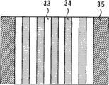
In order to address the above problem, use the dummy that constitutes by Si etc. usually.That is, as shown in Figure 8, when end face applies, dummy 33 and dummy 34 alternately arranged be arranged at anchor clamps 35, make laser strip directly contact (for example referring to patent documentation 1) each other.
Patent documentation 1: the spy opens the 2000-133871 communique
Summary of the invention
But, the common used dummy problem that can cause manufacturing cost to improve and place the quantity of the laser strip of anchor clamps to reduce.
The present invention is in order to address the above problem, and its purpose is, obtains not use dummy can prevent that laser strip from the semiconductor Laser device of thermo-compressed taking place each other when carrying out the end face coating.
Semiconductor Laser device of the present invention has the surface electrode by gold-plated formation, backplate by gold-plated formation, only on surface electrode, form, by anti-adhesion film that does not constitute with the material of Au reaction and the coated film that covers emission side end face and opposition side end face thereof.Further feature of the present invention below is described in detail in detail.
According to the present invention, when carrying out the end face coating, do not use dummy can prevent that laser strip from thermo-compressed taking place each other.And, owing to do not need dummy, thereby can reduce manufacturing cost, and place quantity is set also can increases and improved production capacity of laser strip between anchor clamps.
Description of drawings
Fig. 1 relates to the exterior view of the semiconductor Laser device of embodiment of the present invention 1.
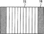
Fig. 2 is the ideograph that the laser strip of a plurality of semiconductor Laser devices in a row of the present invention of expression is arranged at the state in the anchor clamps.
Fig. 3 relates to the exterior view of the semiconductor Laser device of embodiment of the present invention 2.
Fig. 4 relates to the exterior view of the semiconductor Laser device of embodiment of the present invention 3.
Fig. 5 relates to the back view of the semiconductor Laser device of embodiment of the present invention 4.
Fig. 6 relates to the back view of the semiconductor Laser device of embodiment of the present invention 5.
Fig. 7 is the exterior view of conventional semiconductor laser diode.
Fig. 8 is the ideograph that the laser strip of a plurality of conventional semiconductor laser diodes in a row of expression places the state of anchor clamps.
The explanation of symbol
11 Semiconductor substrate
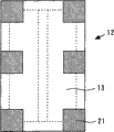
12 semiconductor Laser devices
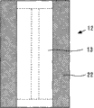
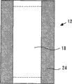
13 surface electrodes
14, the anti-adhesion film of 21-24
15 laser strip
16 anchor clamps
17 laser bodies
18 backplates
19 coated film
Embodiment
Below, the manufacture method that just relates to the semiconductor Laser device of embodiments of the present invention 1 describes.
At first, utilize MBE crystalline growth device or MOCVD crystalline growth device on Semiconductor substrate, to form the sandwich construction that can produce laser generation.Secondly, form surface electrode, and form backplate by the gold-plated back side in Semiconductor substrate by gold-plated surface in Semiconductor substrate.Like this, shown in Fig. 1 (a), in Semiconductor substrate 11, form a plurality of semiconductor Laser devices 12 that are rectangular arrangement.
Then, shown in Fig. 1 (b), only on four jiaos on the surface electrode 13 of each semiconductor Laser device 12,, form anti-adhesion film 14 by the method for evaporation or sputter.This anti-adhesion film 14 particularly, is dielectric film or Pt film by not constituting with the material of Au reaction.Thickness is below the above 5 μ m of 0.05 μ m.If be thinner than 0.05 μ m, can cause the decline of anti-adhesion effect; If be thicker than 5 μ m, peeling off of anti-adhesion film self then may be taken place.
Then, shown in Fig. 2 (a), by this Semiconductor substrate is rived, formation has a plurality of laser strip 15 of exposing the semiconductor Laser device in a row 12 of end face.
Then, shown in Fig. 2 (b), with overlapping so that its emission side end face of a plurality of laser strip 15 up, and with anchor clamps 16 clampings.Subsequently, will be delivered to film formation device with a plurality of laser strip of anchor clamps clamping.Then, by methods such as sputtering method, vacuum vapour deposition or CVD methods, at the emission side end face formation SiO of laser strip
2Deng coated film.Similarly, the opposition side end face in laser strip forms coated film.
When carrying out this end face working procedure of coating,, can directly not contact because the surface electrode and the backplate of adjacent laser strip are separated by anti-adhesion film., anti-adhesion film contacts with the backplate of adjacent laser strip.But because anti-adhesion film is by not constituting with the material of Au reaction, so thermo-compressed can not take place even contact with backplate yet.
After the end face working procedure of coating is finished, a plurality of laser strip are separated from each other.Then, laser strip is divided into semiconductor Laser device one by one, obtains semiconductor Laser device.
Shown in Fig. 2 (c), the semiconductor Laser device 12 of Huo Deing has the laser bodies 17 that is formed with the sandwich construction that can produce laser generation in this way; By the gold-plated surface electrode 13 that forms on the surface of laser bodies 17; By the gold-plated backplate 18 that forms at the back side of laser bodies 17; Only on surface electrode 13, form, by the anti-adhesion film 14 that does not constitute with the material of Au reaction; With the coated film 19 that covers emission side end face and opposition side end face thereof.And anti-adhesion film 14 forms on four jiaos of surface electrode 13.When the width of LD element was 200 μ m, the width of anti-adhesion film was below the 90 μ m.If the width of anti-adhesion film, then can cover near the active layer the LD element center greater than 90 μ m, the vibration of LD is caused bad influence.
According to semiconductor Laser device that relates to embodiments of the present invention 1 and manufacture method thereof, can prevent that adjacent laser strip from thermo-compressed taking place each other.And, owing to do not need dummy, thereby can reduce manufacturing cost, and the quantity that is provided with that has increased the laser strip that places between anchor clamps has improved production capacity.
Execution mode 2
In the manufacture method of the semiconductor Laser device that relates to embodiments of the present invention 2, the generation type of the anti-adhesion film on each semiconductor Laser device that forms on the Semiconductor substrate is different with execution mode 1.As shown in Figure 3, in execution mode 2, four jiaos and the central authorities of dual-side on the surface electrode 13 of semiconductor Laser device 12 by the method for evaporation or sputter, form anti-adhesion film 21.This anti-adhesion film 21 particularly, is dielectric film or Pt film by not constituting with the material of Au reaction.At this moment, thickness is below the above 5 μ m of 0.05 μ m.If be thinner than 0.05 μ m, can cause the decline of anti-adhesion effect; If be thicker than 5 μ m, peeling off of anti-adhesion film self then may be taken place.And when the width of LD element was 200 μ m, the width of anti-adhesion film was below the 90 μ m.If the width of anti-adhesion film, then can cover near the active layer the LD element center greater than 90 μ m, the vibration of LD is caused bad influence.
In this way the semiconductor Laser device of Huo Deing have only on surface electrode, form, by the anti-adhesion film that does not constitute with the material of Au reaction.As shown in Figure 3, has the anti-adhesion film 21 that the central authorities at four jiaos of surface electrode 13 and dual-side form.Other formation is identical with the semiconductor Laser device that relates to execution mode 1.
Relate to the semiconductor Laser device of embodiment of the present invention 2 and manufacture method thereof and not only can reach the effect identical with execution mode 1, and because when a plurality of laser strip place between the anchor clamps, be difficult for concentrated stress on each semiconductor Laser device, can also prevent the damage of each semiconductor Laser device.
Execution mode 3
In the manufacture method of the semiconductor Laser device that relates to embodiments of the present invention 3, the generation type of the anti-adhesion film on each semiconductor Laser device that forms on the Semiconductor substrate is different with execution mode 1.As shown in Figure 4, in execution mode 3,,, form anti-adhesion film 22 by the method for evaporation or sputter along the dual-side on the surface electrode 13 of semiconductor Laser device 12.This anti-adhesion film 22 particularly, is dielectric film or Pt film by not constituting with the material of Au reaction.At this moment, thickness is below the above 5 μ m of 0.05 μ m.If be thinner than 0.05 μ m, can cause the decline of anti-adhesion effect; If be thicker than 5 μ m, peeling off of anti-adhesion film self then may be taken place.And when the width of LD element was 200 μ m, the width of anti-adhesion film was below the 90 μ m.If the width of anti-adhesion film, then can cover near the active layer the LD element center greater than 90 μ m, the vibration of LD is caused bad influence.
In this way the semiconductor Laser device of Huo Deing have only on surface electrode, form, by the anti-adhesion film that does not constitute with the material of Au reaction.As shown in Figure 4, has the anti-adhesion film 22 that the dual-side on surface electrode 13 forms.Other formation is identical with the semiconductor Laser device that relates to execution mode 1.
Relate to the semiconductor Laser device of embodiment of the present invention 3 and manufacture method thereof and not only can reach the effect identical, and when semiconductor Laser device is installed on module etc., can also improve the wettability of scolder with execution mode 1.
Execution mode 4
In the manufacture method of the semiconductor Laser device that relates to embodiments of the present invention 4, the formation pattern of the anti-adhesion film on each semiconductor Laser device that forms on the Semiconductor substrate is different with execution mode 1.As shown in Figure 5, in execution mode 4,,, form anti-adhesion film 23 by the method for evaporation or sputter along the emission side of the backplate 18 of semiconductor Laser device 12 and the both sides of its opposition side.This anti-adhesion film 23 particularly, is dielectric film or Pt film by not constituting with the material of Au reaction.At this moment, thickness is below the above 5 μ m of 0.05 μ m.If be thinner than 0.05 μ m, can cause the decline of anti-adhesion effect; If be thicker than 5 μ m, peeling off of anti-adhesion film self then may be taken place.In addition, because the size of the scolder of electrode connecting line is about 80 μ m, the electrode exposed portions serve of the 80 μ m that need have an appointment.
In this way the semiconductor Laser device of Huo Deing only have form on the electrode overleaf, by the anti-adhesion film that does not constitute with the material of Au reaction.As shown in Figure 5, has the anti-adhesion film 23 that the both sides of the emission side of electrode 18 overleaf and its opposition side form.In addition, on surface electrode, do not form anti-adhesion film.Other formation is identical with the semiconductor Laser device that relates to execution mode 1.
Relate to the semiconductor Laser device of embodiment of the present invention 4 and manufacture method thereof and not only can reach the effect identical with execution mode 1, and the effect of the thermal diffusivity when not influencing laser generation in addition.
Execution mode 5
In the manufacture method of the semiconductor Laser device that relates to embodiments of the present invention 5, the generation type of the anti-adhesion film on each semiconductor Laser device that forms on the Semiconductor substrate is different with execution mode 1.As shown in Figure 6, in execution mode 5,,, form anti-adhesion film 24 by the method for evaporation or sputter along the dual-side on the backplate 18 of semiconductor Laser device 12.This anti-adhesion film 24 particularly, is dielectric film or Pt film by not constituting with the material of Au reaction.At this moment, thickness is below the above 5 μ m of 0.05 μ m.If be thinner than 0.05 μ m, can cause the decline of anti-adhesion effect; If be thicker than 5 μ m, peeling off of anti-adhesion film self then may be taken place.In addition, because the size of the scolder of electrode connecting line is about 80 μ m, the electrode exposed portions serve of the 80 μ m that need have an appointment.
In this way the semiconductor Laser device of Huo Deing only have form on the electrode overleaf, by the anti-adhesion film that does not constitute with the material of Au reaction.As shown in Figure 6, has the anti-adhesion film 24 that forms on the dual-side of electrode 18 overleaf.In addition, on surface electrode, do not form anti-adhesion film.Other formation is identical with the semiconductor Laser device that relates to execution mode 1.
Relate to the semiconductor Laser device of embodiment of the present invention 5 and manufacture method thereof and can reach the effect identical with execution mode 1.
Claims (9)
1. a semiconductor Laser device is characterized by, and comprising:
Surface electrode by gold-plated formation;
Backplate by gold-plated formation;
Only form on the above-mentioned surface electrode, by do not constitute with the material of Au reaction, thickness is the anti-adhesion film below the 5 μ m more than the 0.05 μ m; With
Cover the coated film of emission side end face and opposition side end face thereof.
2. the described semiconductor Laser device of claim 1 is characterized by, and described anti-adhesion film is formed on four jiaos of described surface electrode.
3. the described semiconductor Laser device of claim 1 is characterized by, and described anti-adhesion film is formed on four jiaos and the central authorities of both sides of described surface electrode.
4. the described semiconductor Laser device of claim 1 is characterized by, and forms described anti-adhesion film along the dual-side of described surface electrode.
5. a semiconductor Laser device is characterized by, and comprising:
Surface electrode by gold-plated formation;
Backplate by gold-plated formation;
Only form on the above-mentioned backplate, by do not constitute with the material of Au reaction, thickness is the anti-adhesion film below the 5 μ m more than the 0.05 μ m; With
Cover the coated film of emission side end face and opposition side end face thereof.
6. the described semiconductor Laser device of claim 5 is characterized by, and forms described anti-adhesion film along the dual-side of described backplate.
7. the described semiconductor Laser device of claim 5 is characterized by, and forms described anti-adhesion film along the emission side of described backplate and the both sides of opposition side thereof.
8. any described semiconductor Laser device of claim 1~7 is characterized by, and described anti-adhesion film is dielectric film or Pt film.
9. any described semiconductor Laser device of claim 1~7 is characterized by, and described anti-adhesion film is the film that forms by vapour deposition method or sputtering method.
Applications Claiming Priority (6)
| Application Number | Priority Date | Filing Date | Title |
|---|---|---|---|
| JP2004112254 | 2004-04-06 | ||
| JP112254/2004 | 2004-04-06 | ||
| JP112254/04 | 2004-04-06 | ||
| JP2004372897A JP4594070B2 (en) | 2004-04-06 | 2004-12-24 | Semiconductor laser device and manufacturing method thereof |
| JP372897/04 | 2004-12-24 | ||
| JP372897/2004 | 2004-12-24 |
Publications (2)
| Publication Number | Publication Date |
|---|---|
| CN1681172A CN1681172A (en) | 2005-10-12 |
| CN100592587C true CN100592587C (en) | 2010-02-24 |
Family
ID=35054913
Family Applications (1)
| Application Number | Title | Priority Date | Filing Date |
|---|---|---|---|
| CN200510062896A Active CN100592587C (en) | 2004-04-06 | 2005-04-05 | Semiconductor laser device |
Country Status (4)
| Country | Link |
|---|---|
| US (2) | US7420998B2 (en) |
| JP (1) | JP4594070B2 (en) |
| CN (1) | CN100592587C (en) |
| TW (1) | TWI268032B (en) |
Families Citing this family (5)
| Publication number | Priority date | Publication date | Assignee | Title |
|---|---|---|---|---|
| JP4930322B2 (en) * | 2006-11-10 | 2012-05-16 | ソニー株式会社 | Semiconductor light emitting device, optical pickup device, and information recording / reproducing device |
| DE102007011564B4 (en) * | 2007-03-07 | 2019-08-22 | Jenoptik Optical Systems Gmbh | Method for improved production of diode laser bars |
| JP2009238820A (en) * | 2008-03-26 | 2009-10-15 | Sony Corp | Semiconductor laser device, and manufacturing method of the same |
| US9952388B2 (en) * | 2012-09-16 | 2018-04-24 | Shalom Wertsberger | Nano-scale continuous resonance trap refractor based splitter, combiner, and reflector |
| JP6089902B2 (en) * | 2013-04-11 | 2017-03-08 | 三菱電機株式会社 | Manufacturing method of semiconductor device |
Family Cites Families (14)
| Publication number | Priority date | Publication date | Assignee | Title |
|---|---|---|---|---|
| JPS5929486A (en) * | 1982-08-11 | 1984-02-16 | Fujitsu Ltd | Manufacture of semiconductor laser element |
| JPH0613813B2 (en) * | 1986-07-22 | 1994-02-23 | 吉田工業株式会社 | Storage / drawing device for shutters |
| JPH0730095A (en) | 1993-06-25 | 1995-01-31 | Mitsubishi Electric Corp | Semiconductor device and manufacture thereof |
| JP3116675B2 (en) * | 1993-07-28 | 2000-12-11 | ソニー株式会社 | Semiconductor laser |
| JPH09167873A (en) * | 1995-12-15 | 1997-06-24 | Mitsubishi Electric Corp | Semiconductor laser device |
| KR19980069992A (en) * | 1997-01-20 | 1998-10-26 | 사와무라시코우 | Method for mounting a compound unit of an optical semiconductor device and a support substrate and an optical semiconductor device on a support substrate |
| US6281524B1 (en) * | 1997-02-21 | 2001-08-28 | Kabushiki Kaisha Toshiba | Semiconductor light-emitting device |
| JP3661919B2 (en) | 1998-10-27 | 2005-06-22 | シャープ株式会社 | Manufacturing method of semiconductor laser device |
| JP2001068782A (en) | 1999-08-31 | 2001-03-16 | Matsushita Electronics Industry Corp | Semiconductor light-emitting device and manufacture thereof |
| WO2001040540A1 (en) * | 1999-12-02 | 2001-06-07 | Tegal Corporation | Improved reactor with heated and textured electrodes and surfaces |
| JP3505478B2 (en) * | 2000-06-28 | 2004-03-08 | 三洋電機株式会社 | Nitride-based semiconductor laser device and method of manufacturing nitride-based semiconductor laser device |
| JP2002203499A (en) * | 2000-12-28 | 2002-07-19 | Pioneer Electronic Corp | Electron emission element flat panel display device |
| JP2003209318A (en) * | 2001-11-12 | 2003-07-25 | Sharp Corp | Semiconductor laser element and manufacturing method thereof |
| JP4830315B2 (en) * | 2004-03-05 | 2011-12-07 | 日亜化学工業株式会社 | Semiconductor laser element |
-
2004
- 2004-12-24 JP JP2004372897A patent/JP4594070B2/en active Active
-
2005
- 2005-03-11 TW TW094107484A patent/TWI268032B/en active
- 2005-03-23 US US11/086,440 patent/US7420998B2/en active Active
- 2005-04-05 CN CN200510062896A patent/CN100592587C/en active Active
-
2007
- 2007-06-15 US US11/763,640 patent/US7664152B2/en active Active
Also Published As
| Publication number | Publication date |
|---|---|
| TWI268032B (en) | 2006-12-01 |
| US7420998B2 (en) | 2008-09-02 |
| US20050221549A1 (en) | 2005-10-06 |
| US7664152B2 (en) | 2010-02-16 |
| JP4594070B2 (en) | 2010-12-08 |
| CN1681172A (en) | 2005-10-12 |
| TW200534553A (en) | 2005-10-16 |
| US20080198889A1 (en) | 2008-08-21 |
| JP2005322881A (en) | 2005-11-17 |
Similar Documents
| Publication | Publication Date | Title |
|---|---|---|
| CN100592587C (en) | Semiconductor laser device | |
| US20040130263A1 (en) | High brightness led and method for producing the same | |
| US20060226434A1 (en) | Nitride-based semiconductor light emitting device and manufacturing method thereof | |
| CN101740694A (en) | Light emitting device and method of fabricating light emitting device | |
| JP2013544953A (en) | Thin film encapsulant, optoelectronic semiconductor substrate provided with thin film encapsulant, and method for manufacturing thin film encapsulant | |
| JP5551131B2 (en) | Manufacturing method of nitride semiconductor multilayer structure | |
| US7136407B2 (en) | Semiconductor laser diode with removable high reflection film and method of manufacturing the same | |
| JP4878201B2 (en) | Semiconductor laser device and manufacturing method thereof | |
| JP3307186B2 (en) | Jig for semiconductor surface treatment | |
| JP5744054B2 (en) | Method for manufacturing a semiconductor substrate | |
| KR102089499B1 (en) | Semiconductor light emitting device and method of manufacturing the same | |
| JP2000077726A (en) | Semiconductor element and manufacture thereof | |
| JP4865130B2 (en) | Electrode for semiconductor device and manufacturing method thereof | |
| US5989637A (en) | Method for preventing facet coating overspray | |
| JPS61185993A (en) | Semiconductor laser device | |
| JP2002246679A (en) | Semiconductor laser element and manufacturing method therefor | |
| JPH0897496A (en) | Semiconductor laser and its manufacture | |
| JP2000150958A (en) | Semiconductor light emitting device | |
| JPH0983061A (en) | Method and system for fabricating semiconductor laser element | |
| JP2000252284A (en) | Semiconductor device and manufacture thereof | |
| JP2006066739A (en) | Sub-mount and method for manufacturing same | |
| JPH0546285Y2 (en) | ||
| JPH08236690A (en) | Three-dimensional mounting module and manufacture thereof | |
| CN100377457C (en) | Double-wavelength semiconductor laser luminous device and manufacturing method thereof | |
| JP6616632B2 (en) | Thin film compound solar cell, thin film compound solar cell manufacturing method, thin film compound solar cell array, and thin film compound solar cell array manufacturing method |
Legal Events
| Date | Code | Title | Description |
|---|---|---|---|
| C06 | Publication | ||
| PB01 | Publication | ||
| C10 | Entry into substantive examination | ||
| SE01 | Entry into force of request for substantive examination | ||
| C14 | Grant of patent or utility model | ||
| GR01 | Patent grant |