JP6616632B2 - Thin film compound solar cell, thin film compound solar cell manufacturing method, thin film compound solar cell array, and thin film compound solar cell array manufacturing method - Google Patents
Thin film compound solar cell, thin film compound solar cell manufacturing method, thin film compound solar cell array, and thin film compound solar cell array manufacturing method Download PDFInfo
- Publication number
- JP6616632B2 JP6616632B2 JP2015174333A JP2015174333A JP6616632B2 JP 6616632 B2 JP6616632 B2 JP 6616632B2 JP 2015174333 A JP2015174333 A JP 2015174333A JP 2015174333 A JP2015174333 A JP 2015174333A JP 6616632 B2 JP6616632 B2 JP 6616632B2
- Authority
- JP
- Japan
- Prior art keywords
- layer
- solar cell
- thin film
- film compound
- substrate
- Prior art date
- Legal status (The legal status is an assumption and is not a legal conclusion. Google has not performed a legal analysis and makes no representation as to the accuracy of the status listed.)
- Expired - Fee Related
Links
Images

Classifications
-
- Y—GENERAL TAGGING OF NEW TECHNOLOGICAL DEVELOPMENTS; GENERAL TAGGING OF CROSS-SECTIONAL TECHNOLOGIES SPANNING OVER SEVERAL SECTIONS OF THE IPC; TECHNICAL SUBJECTS COVERED BY FORMER USPC CROSS-REFERENCE ART COLLECTIONS [XRACs] AND DIGESTS
- Y02—TECHNOLOGIES OR APPLICATIONS FOR MITIGATION OR ADAPTATION AGAINST CLIMATE CHANGE
- Y02P—CLIMATE CHANGE MITIGATION TECHNOLOGIES IN THE PRODUCTION OR PROCESSING OF GOODS
- Y02P70/00—Climate change mitigation technologies in the production process for final industrial or consumer products
- Y02P70/50—Manufacturing or production processes characterised by the final manufactured product
Landscapes
- Photovoltaic Devices (AREA)
Description
本発明は、薄膜化合物太陽電池、薄膜化合物太陽電池の製造方法、薄膜化合物太陽電池アレイおよび薄膜化合物太陽電池アレイの製造方法に関する。 The present invention relates to a thin film compound solar cell, a method for manufacturing a thin film compound solar cell, a thin film compound solar cell array, and a method for manufacturing a thin film compound solar cell array.
従来の薄膜化合物太陽電池の製造方法は、基板をエッチングにより除去していたため、基板の厚みが厚いほど製造コストが高くなるという問題があった。このような問題を解決するための手法として、エピタキシャルリフトオフと呼ばれる技術がある。 Since the conventional method for manufacturing a thin film compound solar cell has removed the substrate by etching, there is a problem that the manufacturing cost increases as the thickness of the substrate increases. As a technique for solving such a problem, there is a technique called epitaxial lift-off.
エピタキシャルリフトオフとは、基板と化合物半導体層との間に犠牲層を作製し、かかる犠牲層をエッチャントによって除去することにより、基板と化合物半導体層とを分離するというものである。たとえば特許文献1および特許文献2には、エピタキシャルリフトオフプロセスが開示されている。
The epitaxial lift-off means that a sacrificial layer is produced between the substrate and the compound semiconductor layer, and the sacrificial layer is removed by an etchant to separate the substrate and the compound semiconductor layer. For example,
特許文献1には、第1の基板上に、1つ以上の第1の保護層を成長させることと、AlAs層を成長させることと、1つ以上の第2の保護層を成長させることと、第2の保護層上に少なくとも1つの活性光起電性セル層を堆積することと、活性光起電性セル層の上部を金属でコートすることと、第2の基板を金属でコートすることと、2つの金属表面を互いに押し付けて冷間圧接接合させることと、AlAs層を選択的化学エッチングで除去すること、を含むエピタキシャルリフトオフ処理を実行する方法が記載されている。また、特許文献2には、活性層上に、かつ該活性層に直接的に接触させて、金属バッキング層を形成し、III-V化合物薄膜太陽電池を該基板から分離するために、該活性層と該基板との間から該犠牲層を除去する工程を含むIII-V化合物薄膜太陽電池の加工方法が記載されている。
ここで、半導体基板上に、多接合型化合物半導体太陽電池の非受光側になる層から順に積層する製法を順積みと呼び、このように形成された構造を順積型と呼ぶ。順積型は、たとえば、図11(a)に示すように、基板上にバッファ層、犠牲層、エッチングストップ層、コンタクト層、GaAs太陽電池層、トンネル層、InGaP太陽電池層、コンタクト層の順に積層される。一方、多接合型化合物半導体太陽電池の受光側になる層から順に積層する製法を逆積みと呼び、このように形成された構造を逆積型と呼ぶ。逆積型は、たとえば、図11(b)に示すように、基板上にバッファ層、犠牲層、エッチングストップ層、コンタクト層、InGaP太陽電池層、トンネル層、GaAs太陽電池層、コンタクト層の順に積層される。 Here, the manufacturing method in which layers are stacked in order from the non-light-receiving side of the multi-junction compound semiconductor solar battery on the semiconductor substrate is called “sequential stacking”, and the structure formed in this way is called “sequential stacking”. For example, as shown in FIG. 11A, the sequential product type is in the order of a buffer layer, a sacrificial layer, an etching stop layer, a contact layer, a GaAs solar cell layer, a tunnel layer, an InGaP solar cell layer, and a contact layer on a substrate. Laminated. On the other hand, a manufacturing method in which layers are stacked in order from the light receiving side of a multi-junction compound semiconductor solar battery is called reverse stacking, and the structure formed in this way is called reverse stacking. In the reverse product type, for example, as shown in FIG. 11B, a buffer layer, a sacrificial layer, an etching stop layer, a contact layer, an InGaP solar cell layer, a tunnel layer, a GaAs solar cell layer, and a contact layer are formed on the substrate in this order. Laminated.
特許文献1および特許文献2に記載の方法は、逆積みである。特許文献1の冷間圧接接合させた金属層は活性光起電性セル層の上部に、特許文献2の金属バッキング層は活性層上に、それぞれ全面的に形成されることになり、これらの金属層側を受光面として太陽電池を構成することはできない。
The methods described in
したがって、特許文献1および特許文献2に記載の方法を、たとえば図11(a)に示すような2以上のpn接合の順積型に適用することができないという問題がある。
Therefore, there is a problem that the methods described in
本発明は、上記のような現状に鑑みてなされたものであり、その目的とするところは、順積型での製造が可能な薄膜化合物太陽電池および薄膜化合物太陽電池アレイを提供することである。 The present invention has been made in view of the above situation, and an object of the present invention is to provide a thin-film compound solar cell and a thin-film compound solar cell array that can be manufactured in a stacked product type. .
上記課題を解決するため、本発明は、基板上に、1以上のpn接合を有する太陽電池層を形成するステップと、太陽電池層上に表面電極層を形成するステップと、太陽電池層および表面電極層を透明材料で被覆するステップと、基板を除去するステップと、太陽電池層の一部を除去して表面電極層を露出させるステップとを含む、薄膜化合物太陽電池の製造方法とする。 In order to solve the above problems, the present invention provides a step of forming a solar cell layer having one or more pn junctions on a substrate, a step of forming a surface electrode layer on the solar cell layer, a solar cell layer and a surface A method for manufacturing a thin film compound solar cell includes a step of covering the electrode layer with a transparent material, a step of removing the substrate, and a step of removing a part of the solar cell layer to expose the surface electrode layer.
好ましくは、太陽電池層はpn接合を有するサブセルを複数備え、太陽電池層を形成するステップは、基板上に第1のサブセルを形成するステップと、第1のサブセル上に第2のサブセルを形成するステップを含み、第2のサブセルのバンドギャップは、前記第1のサブセルのバンドギャップよりも大きい。 Preferably, the solar cell layer includes a plurality of subcells having a pn junction, and the step of forming the solar cell layer includes forming a first subcell on the substrate and forming a second subcell on the first subcell. The band gap of the second subcell is greater than the bandgap of the first subcell.
好ましくは、基板と太陽電池層との間に犠牲層を形成するステップを更に含み、基板を除去するステップにおいて、犠牲層をエッチングすることにより、基板を分離することとしてもよい。 Preferably, the method may further include a step of forming a sacrificial layer between the substrate and the solar cell layer, and in the step of removing the substrate, the sacrificial layer may be etched to separate the substrate.
好ましくは、基板と太陽電池層との間にエッチングストップ層を形成するステップを更に含み、基板を除去するステップにおいて、基板をエッチング除去することとしてもよい。 Preferably, the method may further include a step of forming an etching stop layer between the substrate and the solar cell layer, and the substrate may be removed by etching in the step of removing the substrate.
また、化合物半導体からなる1以上のpn接合を有する太陽電池層と、太陽電池層の受光側に配置された表面電極層と、太陽電池層および表面電極層の受光側を被覆する透明材料とを備え、非受光側において、表面電極層の一部に太陽電池層と透明材料とが配置されない領域を有する、薄膜化合物太陽電池とする。 Moreover, the solar cell layer which has one or more pn junctions which consist of a compound semiconductor, The surface electrode layer arrange | positioned at the light-receiving side of a solar cell layer, The transparent material which coat | covers the light-receiving side of a solar cell layer and a surface electrode layer It is set as the thin film compound solar cell which has the area | region where a solar cell layer and a transparent material are not provided in a part of surface electrode layer in the non-light-receiving side.
また、化合物半導体からなる1以上のpn接合を有する太陽電池層と、太陽電池層の受光側に配置された表面電極層と、太陽電池層および表面電極層の受光側を被覆する透明材料とを備え、非受光側において、表面電極層の一部に太陽電池層と透明材料とが配置されない領域を有する薄膜化合物太陽電池の複数を、フィルムの一方の面側に配線を有する配線シート上に配置するステップと、薄膜化合物太陽電池の電極と配線とが電気的に接続されるように配線シートと薄膜化合物太陽電池を接着するステップとを含む、薄膜化合物太陽電池アレイの製造方法とする。 Moreover, the solar cell layer which has one or more pn junctions which consist of a compound semiconductor, The surface electrode layer arrange | positioned at the light-receiving side of a solar cell layer, The transparent material which coat | covers the light-receiving side of a solar cell layer and a surface electrode layer A plurality of thin-film compound solar cells having a region where the solar cell layer and the transparent material are not arranged on a part of the surface electrode layer on the non-light-receiving side are arranged on a wiring sheet having wiring on one surface side of the film And a step of bonding the wiring sheet and the thin film compound solar cell so that the electrode of the thin film compound solar cell and the wiring are electrically connected to each other.
また、化合物半導体からなる1以上のpn接合を有する太陽電池層と、太陽電池層の受光側に配置された表面電極層と、太陽電池層および表面電極層の受光側を被覆する透明材料とを備え、非受光側において、表面電極層の一部に太陽電池層と透明材料とが配置されない領域を有する薄膜化合物太陽電池の複数と、フィルムの一方の面側に薄膜化合物太陽電池の電極と電気的に接続された配線を有する配線シートとを備える、薄膜化合物太陽電池アレイとする。 Moreover, the solar cell layer which has one or more pn junctions which consist of a compound semiconductor, The surface electrode layer arrange | positioned at the light-receiving side of a solar cell layer, The transparent material which coat | covers the light-receiving side of a solar cell layer and a surface electrode layer A plurality of thin-film compound solar cells having a region in which the solar cell layer and the transparent material are not disposed on a part of the surface electrode layer on the non-light-receiving side, and the electrodes of the thin-film compound solar cell and the electricity on one surface side of the film A thin-film compound solar cell array including a wiring sheet having wirings connected to each other.
本発明は、上記のような構成を有することにより、順積型での製造が可能な薄膜化合物太陽電池および薄膜太陽電池アレイを提供する。 The present invention provides a thin-film compound solar cell and a thin-film solar cell array that can be manufactured in a sequential product type by having the above-described configuration.
以下、本発明の実施の形態について図面を用いて説明する。なお、実施の形態の図面において、同一の参照符号は、同一部分または相当部分を表わすものである。また、長さ、幅、厚さ、深さなどの寸法関係は図面の明瞭化と簡略化のために適宜に変更されており、実際の寸法関係を表わすものではない。 Hereinafter, embodiments of the present invention will be described with reference to the drawings. In the drawings of the embodiment, the same reference numerals represent the same or corresponding parts. In addition, dimensional relationships such as length, width, thickness, and depth are changed as appropriate for clarity and simplification of the drawings, and do not represent actual dimensional relationships.
(実施の形態1)
<薄膜化合物太陽電池の製造方法>
実施の形態1の薄膜化合物太陽電池の製造方法は、基板10上に、犠牲層20および1以上のpn接合を有する太陽電池層30を形成するステップ(図1)と、該太陽電池層30の側面をエッチングにより除去するステップ(図2)と、該太陽電池層30上に部分的に表面電極層40を形成するステップと(図3)と、該太陽電池層30および該表面電極層40を透明材料50で被覆するステップ(図4)と、犠牲層20をエッチングにより除去することにより、基板10を除去するステップ(図5)と、該太陽電池層30の一部を除去して表面電極層を露出させるステップ(図6)とを含む。
(Embodiment 1)
<Method for Manufacturing Thin Film Compound Solar Cell>
In the method for manufacturing a thin film compound solar cell according to the first embodiment, a step (FIG. 1) of forming a
上記のような各ステップを用いて薄膜化合物太陽電池を作製することにより、太陽電池層30の基板10と反対側の面を受光面とすることができる。すなわち、2以上のpn接合を有する太陽電池層を順積型の構造とすることができる。
By producing a thin film compound solar cell using the steps as described above, the surface of the
本実施の形態の製造方法は、基板上に、1以上のpn接合を有する太陽電池層を形成するステップと、太陽電池層上に表面電極層を形成するステップと、太陽電池層および表面電極層を透明材料で被覆するステップと、基板を除去するステップと、太陽電池層の一部を除去して表面電極層を露出させるステップとを含む。そのため、太陽電池層30の基板10と反対側に部分的に表面電極層40が形成され、また、透明材料50が配置されるので、太陽電池層30の基板10と反対側の面を受光面とすることができる。さらに、本実施の形態の製造方法により得られた太陽電池は、太陽電池の非受光側から、表面電極層40に接続できるので、配線付きフィルムを用いた実装が可能となる。また、太陽電池層30上に配置した透明材料50を太陽電池の表面保護層として利用できるので、複数の太陽電池を電気的に接続して形成するアレイの製造工程における工程数の削減および低コスト化に繋がる。以下においては、図面を参照しつつ本実施の形態の薄膜化合物太陽電池の製造方法を構成する各ステップを説明する。
The manufacturing method of the present embodiment includes a step of forming a solar cell layer having one or more pn junctions on a substrate, a step of forming a surface electrode layer on the solar cell layer, a solar cell layer and a surface electrode layer Covering the substrate with a transparent material, removing the substrate, and removing a portion of the solar cell layer to expose the surface electrode layer. Therefore, the
(化合物半導体層を形成するステップ)
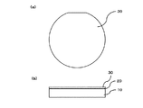
図1は、基板上に化合物半導体層を形成した後の状態を示す図であって、(a)は表面側から見た模式的な平面図であり、(b)は模式的な断面図である。図1に示されるように、基板10上に、有機金属気相成長法(MOCVD:Metal Organic Chemical Vapor Deposition)を用いて、犠牲層を含む層20、太陽電池層30を結晶成長させる。実施の形態1では、図8に示されるように、基板10上に、バッファ層21、犠牲層22、エッチングストップ層23、第1コンタクト層41、ベース層31、エミッタ層32、および第2コンタクト層42の順に、化合物半導体層を結晶成長させる。以下において、ベース層31およびエミッタ層32のことを総称して「太陽電池層30」と記す。また、第1コンタクト層41および第2コンタクト層42のことを総称して「コンタクト層と記す。なお、バッファ層21、犠牲層22、エッチングストップ層23、第1コンタクト層41、ベース層31、エミッタ層32、および第2コンタクト層42のことを総称して「化合物半導体層80」と記す。また、受光側のことを表面側と記す。
(Step of forming a compound semiconductor layer)
FIG. 1 is a diagram showing a state after a compound semiconductor layer is formed on a substrate, where (a) is a schematic plan view seen from the front side, and (b) is a schematic cross-sectional view. is there. As shown in FIG. 1, a
ここで、本実施の形態における基板10は、その上に形成するバッファ層21の下地となるものである。このため、基板10は、バッファ層21と格子定数が近いことが好ましい。このような基板の材料としては、たとえばゲルマニウム(Ge)や、ガリウム砒素(GaAs)等を挙げることができる。
Here, the
また、本実施の形態における犠牲層22は、エッチングされやすい半導体であればいかなるものをも用いることができる。ここで、本実施の形態の「犠牲層」は、基板と化合物半導体層との間に設けられるものであって、その層をエッチングなどで除去することにより、基板と化合物半導体層とを分離するために設けられるものである。このような犠牲層22に用いる半導体としては、たとえばAlAsを挙げることができる。AlAsからなる犠牲層22を用いる場合、犠牲層22をエッチングするためのエッチャントとしては、たとえばフッ酸と水とを1対10の比率で混合したフッ酸水溶液または塩酸を用いることが好ましい。後述するステップで、犠牲層22をエッチングして除去することにより、基板10と化合物半導体層80とを分離する。
In addition, the
本実施の形態におけるエッチングストップ層23は、犠牲層22がエッチングされるときに太陽電池層30およびコンタクト層がエッチャントに曝されないようにするために保護するものである。このようなエッチングストップ層23を構成する材料としては、たとえばInGaPを挙げることができる。
The etching stop layer 23 in the present embodiment protects the
本実施の形態におけるベース層31およびエミッタ層32は、太陽電池層100の構成のうちのpn接合の構造をなすものである。この部分に太陽光が照射されることにより、キャリアが生じて電流が発生する。太陽電池層30はさらに、ベース層31の非受光面側にBSF層(バックサーフェスフィールド層)を備えていてもよく、エミッタ層32の受光面側に窓層を備えていてもよい。
The base layer 31 and the emitter layer 32 in the present embodiment form a pn junction structure in the configuration of the
(太陽電池層の側面をエッチングにより除去するステップ)
図2は、太陽電池層の側面の一部をエッチングで除去した後の状態を示すであり、(a)は表面側から見た模式的な平面図であり、(b)は模式的な断面図である。太陽電池層30の側面をエッチング液でエッチングすることにより、図2に示されるように、犠牲層20の表面の一部を露出させる。このように太陽電池層30の側面をエッチングにより除去することにより、各太陽電池セルが電気的に分離されて、太陽電池セルの領域が確定する。ここでは、2つの太陽電池セル領域(R1、R2)に分離している。また、犠牲層20が露出することにより、エッチング液が犠牲層20に伝わりやすくなり、犠牲層20をエッチングしやすくなる。
(Step of removing the side surface of the solar cell layer by etching)
FIG. 2 shows a state after a part of the side surface of the solar cell layer is removed by etching, (a) is a schematic plan view seen from the surface side, and (b) is a schematic cross section. FIG. By etching the side surface of the
ここで、太陽電池層30の側面をエッチングする方法としては、実施の形態1では、まず、太陽電池層30上に形成された第2コンタクト層42上に保護膜(図示せず)を塗布し、太陽電池層30を残す領域の保護膜をフォトリソグラフィにより残し、それ以外の保護膜を取り除くという方法がある。そして、保護膜でマスキングした領域以外の太陽電池層30をエッチング液でエッチングすることにより、太陽電池層30の側面をエッチングすることができる。その後、保護膜を除去する。
Here, as a method for etching the side surface of the
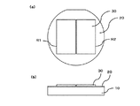
(表面電極層を形成するステップ)
表面電極層40は、太陽電池層30上に部分的に形成される。表面電極層40は、第2コンタクト層と金属からなる表面電極を含む。図3は、第2コンタクト層上に表面電極を形成した後の状態を示す図であって、(a)は表面側から見た模式的な平面図であり、(b)は模式的な断面図である。パターニングされた第2コンタクト層42上に、金属を蒸着することにより表面電極を形成する。表面電極に用いられる材料としては、Ti/Pd/Ag等を挙げることができる。ここで、上記「Ti/Pd/Ag」とは、第2コンタクト層42側から順に、Ti層とPd層とAg層とをこの順に形成することを意味する。また、太陽電池層30上に蒸着等によりARコートを施してもよい。
(Step of forming the surface electrode layer)
The
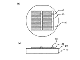
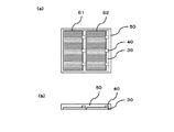
(太陽電池層および表面電極層を透明材料で被覆するステップ)
図4は、太陽電池層および表面電極層を透明材料で被覆した後の状態を示す図であって、(a)は表面側から見た模式的な平面図であり、(b)は模式的な断面図である。図4に示されるように、太陽電池層30および表面電極層40を透明材料50で被覆する。このとき、透明材料50は、2つの太陽電池セルS1およびS2を一体的に被覆する。
(Step of covering solar cell layer and surface electrode layer with transparent material)
FIG. 4 is a diagram illustrating a state after the solar cell layer and the surface electrode layer are covered with a transparent material, in which (a) is a schematic plan view viewed from the surface side, and (b) is a schematic diagram. FIG. As shown in FIG. 4, the
ここで、透明材料50としては、透明樹脂や粘着材付きフィルムなどを用いることができる。透明材料50は、光透過率が高いことが好ましい。透明材料50として透明樹脂を用いる場合は、透明樹脂を塗布・硬化させることで形成する。このとき、透明材料の形成が不要な部分にはマスクなどを施す。透明樹脂としては、モメンティブ・パフォーマンス・マテリアルズ・ジャパン合同会社製IVS4622などがある。また、透明材料50として、粘着材付きフィルムを用いる場合は、予め抜き加工などでフィルムの形を整え、粘着材を介してフィルムを貼り付ける。粘着材としては、光学粘着材を用いることができる。光学粘着材としては、日東電工株式会社製LUCIACS(R)CS986などがある。フィルムとしては、高透過率フィルムを用いることができ、たとえばPENフィルムである。高透過率フィルムとしては、帝人デュポンフィルム株式会社製Q65Hなどがある。
Here, as the
さらに、透明材料50の上面に支持部材を設けてもよい(図示せず)。支持部材を設けることにより、後述の基板を剥離するステップやエッチングストップ層を除去するステップなどのエッチングの作業性を向上させることができる。ここで、支持部材としては、たとえばガラスを好適に用いることができる。 Further, a support member may be provided on the upper surface of the transparent material 50 (not shown). By providing the support member, it is possible to improve the workability of etching such as a step of peeling a substrate described later and a step of removing the etching stop layer. Here, for example, glass can be suitably used as the support member.
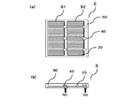
(基板を除去するステップ)
図5は、基板を除去した後の状態を示す図であって、(a)は表面側から見た模式的な平面図であり、(b)は模式的な断面図である。図4に示す積層体をエッチャントに浸漬させることにより、犠牲層22は外側から内側に向かってエッチングされる。このとき、太陽電池層30は透明材料50およびエッチングストップ層23によりエッチャントから保護される。そして、犠牲層22のエッチングが進行して、化合物半導体層80が基板10から離れる。なお、エッチャントとしては上述したように、フッ酸と水とを1対10の比率で混合したフッ酸水溶液または塩酸を用いることが好ましい。犠牲層22のエッチングが完了したときに、基板10と化合物半導体層80とが分離され、化合物半導体層80から基板は除去される。
(Step of removing the substrate)
5A and 5B are diagrams showing a state after removing the substrate, where FIG. 5A is a schematic plan view seen from the surface side, and FIG. 5B is a schematic cross-sectional view. 4 is immersed in an etchant, the
(エッチングストップ層を除去するステップ)
基板10を除去後、エッチングストップ層23をエッチングにより除去する。これにより第1コンタクト層41を露出させる。
(Step of removing the etching stop layer)
After removing the
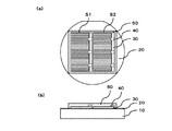
(太陽電池層の一部を除去して表面電極層を露出させるステップ)
図6は、太陽電池層の一部を除去して表面電極層を露出させた後の状態を示す図であって、(a)表面側から見た模式的な平面図であり、(b)模式的な断面図である。図6に示されるように、太陽電池層30の一部を除去し、表面電極層が露出する開口部60を形成する。開口部60において、表面電極層の第2コンタクト層42および表面電極の少なくとも一方が露出している。開口部60は、第1コンタクト層41および太陽電池層30の一部を除去することで形成される。また、開口部60は、第1コンタクト層41、太陽電池層30および第2コンタクト層42の一部を除去することで形成してもよい。
(Step of removing a part of the solar cell layer to expose the surface electrode layer)
FIG. 6 is a view showing a state after a part of the solar cell layer is removed and the surface electrode layer is exposed, (a) a schematic plan view seen from the surface side, (b) It is typical sectional drawing. As shown in FIG. 6, a part of the
ここで、太陽電池層30の一部をエッチングにより除去することができる。エッチング方法としては、まず第1コンタクト層41上に保護膜を塗布し、太陽電池層30を残す領域の保護膜をフォトリソグラフィにより残し、それ以外の保護膜を取り除くという方法がある。そして、保護膜でマスキングした領域以外の太陽電池層30をエッチング液でエッチングすることにより、太陽電池層30の一部をエッチングすることができる。その後、保護膜を除去する。
Here, a part of the
このようにして、図6に示す薄膜化合物太陽電池Aが得られる。図6に示す薄膜化合物太陽電池Sは、2つの太陽電池セル(S1、S2)を含む。薄膜化合物太陽電池Sは、複数の太陽電池セルを含むことにより、薄膜化合物太陽電池アレイの製造工程における工程数の削減に繋がる。また、薄膜化合物太陽電池Sに含まれる複数の太陽電池セルを分離してもかまわない。 Thus, the thin film compound solar cell A shown in FIG. 6 is obtained. The thin film compound solar cell S shown in FIG. 6 includes two solar cells (S1, S2). By including a plurality of solar cells, the thin film compound solar cell S leads to a reduction in the number of steps in the manufacturing process of the thin film compound solar cell array. Moreover, you may isolate | separate the several photovoltaic cell contained in the thin film compound solar cell S. FIG.
(裏面電極を形成するステップ)
得られた薄膜化合物太陽電池に、さらに裏面電極を形成してもよい。裏面電極(図示せず)は、太陽電池層30の非受光側に形成する。裏面電極は、第1コンタクト層41上に金属を蒸着することにより形成することができる。裏面電極に用いられる材料としては、Au/Ag、Ti/Pd/Ag等を挙げることができる。ここで、上記「Au/Ag」とは、第1コンタクト層8側から順に、Au層とAg層とをこの順に形成することを意味する。また、後述のように、配線付きフィルムに接続することで裏面電極を形成することもできる。
(Step of forming the back electrode)
You may form a back electrode further in the obtained thin film compound solar cell. The back electrode (not shown) is formed on the non-light receiving side of the
(実施の形態2)
実施の形態2では、具体例を挙げて実施の形態1をより詳細に説明するが、本発明はこれらに限定されるものではない。
(Embodiment 2)
In the second embodiment, the first embodiment will be described in more detail with specific examples, but the present invention is not limited to these.
実施の形態2の薄膜化合物太陽電池の製造方法は、実施の形態1と同様、基板上に、1以上のpn接合を有する太陽電池層を形成するステップと、太陽電池層上に表面電極層を形成するステップと、太陽電池層および表面電極層を透明材料で被覆するステップと、基板を除去するステップと、太陽電池層の一部を除去して表面電極層を露出させるステップとを含む。
The manufacturing method of the thin film compound solar cell of
(化合物半導体層を形成するステップ)
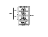
実施の形態2では、図1に示されるように、厚みが400μmのGaAsからなる基板10上に、MOCVD法を用いて10nmの厚みのAlAsを含む犠牲層20、太陽電池層30を形成した。実施の形態2において、基板10上に形成した化合物半導体層80は、図8に示されるように、GaAsからなるバッファ層21、AlAsからなる犠牲層22、InGaPからなるエッチングストップ層23、GaAsからなる第1コンタクト層41、InGaPからなるベース層31およびエミッタ層32、GaAsからなる第2コンタクト層42をこの順に形成したものである。また、太陽電池層30は、第1コンタクト層41、ベース層31、エミッタ層32および第2コンタクト層42をこの順に形成したものであり、ベース層31とエミッタ層32との接合面がpn接合となる。
(Step of forming a compound semiconductor layer)
In the second embodiment, as shown in FIG. 1, a
(太陽電池層の側面をエッチングにより除去するステップ)
次に、図2に示されるように、太陽電池層30の第2コンタクト層42の表面に、レジスト材料である保護膜(図示せず)を塗布し、フォトリソグラフィを用いて第2コンタクト層42よりも若干広い領域だけ保護膜を残し、それ以外の領域の保護膜を取り除く。そして、保護膜でマスキングした領域以外の太陽電池層30の側面をエッチング液でエッチングすることにより、犠牲層20を露出させる。
(Step of removing the side surface of the solar cell layer by etching)
Next, as shown in FIG. 2, a protective film (not shown), which is a resist material, is applied to the surface of the second contact layer 42 of the
(表面電極層を形成するステップ)
次に、図3に示されるように、第2コンタクト層42の表面電極を蒸着させる領域以外の領域をエッチング等で除去した上で、Ti、Pd、Agをこの順で蒸着することにより、第2コンタクト層42上に厚み3μmのTi/Pd/Agからなる表面電極を形成し、表面電極層40を形成した。
(Step of forming the surface electrode layer)
Next, as shown in FIG. 3, after removing regions other than the region where the surface electrode of the second contact layer 42 is deposited by etching or the like, Ti, Pd, and Ag are deposited in this order, thereby 2 A surface electrode made of Ti / Pd / Ag having a thickness of 3 μm was formed on the contact layer 42 to form a
(太陽電池層および表面電極層を透明材料で被覆するステップ)
次いで、図4に示されるように、太陽電池層30および表面電極層40上を透明材料50で被覆した。ここで、透明材料50として、透明樹脂(モメンティブ・パフォーマンス・マテリアルズ・ジャパン合同会社製;IVS4622)を用いた。
(Step of covering solar cell layer and surface electrode layer with transparent material)
Next, as shown in FIG. 4, the
(基板を剥離するステップ)
次に、図4に示される積層体をエッチャントに浸漬させ、犠牲層22を除去した。エッチャントとしては、フッ酸と水とを1対10の比率で混合したフッ酸水溶液を用い、エッチャントの液温を40℃とした。犠牲層3のエッチングが完了したときに、基板10と化合物半導体層80とが分離され、図5に示されるように、透明材料50で被覆された化合物半導体層80が得られた。
(Step of peeling the substrate)
Next, the laminate shown in FIG. 4 was immersed in an etchant, and the
(エッチングストップ層を除去するステップ)
次に、化合物半導体層80のエッチングストップ層23をエッチングを用いて除去した。これにより、透明材料50で被覆された太陽電池層30が得られた。
(Step of removing the etching stop layer)
Next, the etching stop layer 23 of the compound semiconductor layer 80 was removed by etching. Thereby, the
(太陽電池層の一部を除去して表面電極層を露出させるステップ)
図6に示されるように、太陽電池層30の一部を除去することにより、表面電極層が露出するように開口部を形成した。開口部は、第1コンタクト層41、太陽電池層30および第2コンタクト層42までをエッチングにより除去することで形成した。開口部は、第1コンタクト層41および太陽電池層30までをエッチングにより除去することで形成してもよい。また、表面電極層の第2コンタクト層および表面電極の少なくとも一方を露出させればよい。
(Step of removing a part of the solar cell layer to expose the surface electrode layer)
As shown in FIG. 6, by removing a part of the
(裏面電極を形成するステップ)
パターニングされた第1コンタクト層41上に、Au/Agからなる裏面電極を形成した。
(Step of forming the back electrode)
On the patterned first contact layer 41, a back electrode made of Au / Ag was formed.
(実施の形態3)
実施の形態3の薄膜化合物太陽電池の製造方法は、基板上に、エッチングストップ層および1以上のpn接合を有する太陽電池層を形成するステップと、該太陽電池層の側面をエッチングにより除去するステップと、該太陽電池層上に部分的に表面電極層を形成するステップと、該太陽電池層および該表面電極層を透明材料で被覆するステップと、基板1をエッチングにより除去するステップと、エッチングストップ層をエッチングにより除去するステップと、該太陽電池層の一部を除去して表面電極層を露出させるステップを含む。
(Embodiment 3)
The method for manufacturing a thin film compound solar cell according to Embodiment 3 includes a step of forming a solar cell layer having an etching stop layer and one or more pn junctions on a substrate, and a step of removing side surfaces of the solar cell layer by etching. A step of partially forming a surface electrode layer on the solar cell layer, a step of covering the solar cell layer and the surface electrode layer with a transparent material, a step of removing the
実施の形態3の太陽電池の製造方法は、基板上に、1以上のpn接合を有する太陽電池層を形成するステップと、太陽電池層上に表面電極層を形成するステップと、太陽電池層および表面電極層を透明材料で被覆するステップと、基板を除去するステップと、太陽電池層の一部を除去して表面電極層を露出させるステップとを含み、実施の形態1と化合物半導体層を形成するステップと基板を剥離するステップとが異なる以外は、実施の形態1と同様である。
A method for manufacturing a solar cell according to Embodiment 3 includes a step of forming a solar cell layer having one or more pn junctions on a substrate, a step of forming a surface electrode layer on the solar cell layer, a solar cell layer, Forming the compound semiconductor layer according to the first embodiment, comprising: covering the surface electrode layer with a transparent material; removing the substrate; and removing a part of the solar cell layer to expose the surface electrode layer. The steps are the same as those in
(化合物半導体層を形成するステップ)
図9は、実施の形態3の基板上に化合物半導体層を形成した後の状態を示す模式的な断面図である。図9に示されるように、基板91上に、有機金属気相成長法(MOCVD:Metal Organic Chemical Vapor Deposition)を用いて、エッチングストップ層92、太陽電池層900の順に、化合物半導体層90を結晶成長させる。実施の形態3の基板91の構成は、実施の形態1と同様である。また、実施の形態3の太陽電池層900の構成は、第1コンタクト層93、ベース層94、エミッタ層95、および第2コンタクト層96であり、実施の形態1と同様である。
(Step of forming a compound semiconductor layer)
FIG. 9 is a schematic cross-sectional view showing a state after the compound semiconductor layer is formed on the substrate of the third embodiment. As shown in FIG. 9, a compound semiconductor layer 90 is crystallized on a substrate 91 in the order of an etching stop layer 92 and a solar cell layer 900 using metal organic chemical vapor deposition (MOCVD). Grow. The configuration of the substrate 91 of the third embodiment is the same as that of the first embodiment. The configuration of the solar cell layer 900 of the third embodiment is the first contact layer 93, the base layer 94, the emitter layer 95, and the second contact layer 96, and is the same as that of the first embodiment.
実施の形態3におけるエッチングストップ層92は、基板がエッチングされるときに太陽電池層900やコンタクト層がエッチャントに曝されないようにするために保護するものである。このようなエッチングストップ層92を構成する材料としては、たとえばInGaPを挙げることができる。 The etching stop layer 92 in the third embodiment protects the solar cell layer 900 and the contact layer so that they are not exposed to the etchant when the substrate is etched. As a material constituting such an etching stop layer 92, for example, InGaP can be cited.
(基板を除去するステップ)
実施の形態3では、基板91はエッチングにより除去される。このとき、太陽電池層900およびコンタクト層93、96は透明材料50およびエッチングストップ層92によりエッチャントから保護される。
(Step of removing the substrate)
In Embodiment 3, the substrate 91 is removed by etching. At this time, the solar cell layer 900 and the contact layers 93 and 96 are protected from the etchant by the
(実施の形態4)
実施の形態4の太陽電池の製造方法は、基板上に、1以上のpn接合を有する太陽電池層を形成するステップと、太陽電池層上に表面電極層を形成するステップと、太陽電池層および表面電極層を透明材料で被覆するステップと、基板を除去するステップと、太陽電池層の一部を除去して表面電極層を露出させるステップとを含み、実施の形態1と太陽電池層が異なる以外は、実施の形態1と同様である。実施の形態4の太陽電池層は、2つのpn接合を有する順積型の構造である。なお、実施の形態4の太陽電池層は、実施の形態2および実施の形態3にも適用可能である。
(Embodiment 4)
A method for manufacturing a solar cell according to
図10に、実施の形態4の基板上に化合物半導体層を形成した後の状態を示す模式的な断面図を示す。基板101上に、有機金属気相成長法(MOCVD:Metal Organic Chemical Vapor Deposition)を用いて、基板101上に、バッファ層102、犠牲層103、エッチングストップ層104、第1コンタクト層105、BSF層106、ベース層107、エミッタ層108、窓層109、トンネル層110、BSF層111、ベース層112、エミッタ層113、窓層114、第2コンタクト層115の順に、化合物半導体層を結晶成長させる。以下において、BSF層106、ベース層107、エミッタ層108、窓層109、トンネル層110、BSF層111、ベース層112、エミッタ層113、窓層114のことを総称して「太陽電池層1000」と記す。なお、バッファ層102、犠牲層103、エッチングストップ層104、第1コンタクト層105、BSF層106、ベース層107、エミッタ層108、窓層109、トンネル層110、BSF層111、ベース層112、エミッタ層113、窓層114、第2コンタクト層115のことを総称して「化合物半導体層100」と記す。実施の形態4の太陽電池層1000はpn接合を有するサブセルを2つ備える。図10に示されるように、第1のサブセル1100は、BSF層106、GaAsからなるベース層107とエミッタ層108、窓層109を有し、第2のサブセル1200は、BSF層111、InGaPからなるベース層112とエミッタ層113、窓層114を有する。第2のサブセルのバンドギャップは第1のサブセルのバンドギャップよりも大きく、太陽電池層は順積型の構造である。太陽電池層1000の基板と反対側が受光側となる。なお、実施の形態4の各サブセルは、BSF層と窓層を備えているが、これらはなくてもよい。
FIG. 10 is a schematic cross-sectional view showing a state after the compound semiconductor layer is formed on the substrate of the fourth embodiment. A buffer layer 102, a sacrificial layer 103, an etching stop layer 104, a first contact layer 105, and a BSF layer are formed on the substrate 101 using metal organic chemical vapor deposition (MOCVD). The compound semiconductor layer is grown in the order of 106, base layer 107,
(実施の形態5)
<薄膜化合物太陽電池アレイの製造方法>
実施の形態5の薄膜化合物太陽電池アレイの製造方法は、受光側が透明材料で被覆され、非受光側の一部に太陽電池層が除去された開口部を有し、開口部から表面電極層の一部が露出する薄膜化合物太陽電池の複数を、フィルムの一方の面側に配線を有する配線シート上に配置するステップと、薄膜化合物太陽電池の電極と配線が電気的に接続されるように配線シートと薄膜化合物太陽電池を接着するステップとを含む。
(Embodiment 5)
<Method for Producing Thin-Film Compound Solar Cell Array>
In the method of manufacturing the thin-film compound solar cell array according to Embodiment 5, the light receiving side is covered with a transparent material, and the solar cell layer is removed from a part of the non-light receiving side. Arranging a plurality of partially exposed thin film compound solar cells on a wiring sheet having wiring on one side of the film, and wiring so that the electrodes and wiring of the thin film compound solar cell are electrically connected Adhering the sheet and the thin film compound solar cell.
本実施の形態の製造方法は、受光側が透明材料で被覆され、表面電極層に非受光側から配線接続可能な薄膜化合物太陽電池の複数を、配線シートを用いて実装する。薄膜化合物太陽電池を被覆する透明材料は薄膜化合物太陽電池の表面保護層として利用できるので、複数の薄膜化合物太陽電池を電気的に接続して形成するアレイの製造工程における工程数の削減および低コスト化が可能となる。 In the manufacturing method of the present embodiment, a plurality of thin-film compound solar cells whose light-receiving side is covered with a transparent material and can be connected to the surface electrode layer from the non-light-receiving side are mounted using a wiring sheet. Since the transparent material covering the thin film compound solar cell can be used as a surface protective layer of the thin film compound solar cell, the number of steps in the manufacturing process of the array formed by electrically connecting a plurality of thin film compound solar cells and low cost are reduced. Can be realized.
実施の形態5では、実施の形態1の薄膜化合物太陽電池に適用可能な薄膜化合物太陽電池アレイの製造方法について説明する。なお、実施の形態5の製造方法は、実施の形態2、実施の形態3および実施の形態4の薄膜化合物太陽電池にも適用可能である。
In the fifth embodiment, a method for manufacturing a thin film compound solar cell array applicable to the thin film compound solar cell of the first embodiment will be described. In addition, the manufacturing method of Embodiment 5 is applicable also to the thin film compound solar cell of
<薄膜化合物太陽電池>
実施の形態5の薄膜化合物太陽電池としては、実施の形態1の図6に示されるセルを用いることができる。図6に示されるように、実施の形態5に用いる薄膜太陽電池Sは、受光側となる太陽電池層30の上面および表面電極層の上面が透明材料50で被覆されている。一方、非受光側では太陽電池層30の第1コンタクト層41と表面電極層40の一部が露出している。表面電極層の露出部は、太陽電池層30の一部が除去された開口部60により形成されている。第1コンタクト層41および表面電極層40の一部は、後述の配線シートとの接続部となる。
<Thin film compound solar cell>
As the thin film compound solar battery of the fifth embodiment, the cell shown in FIG. 6 of the first embodiment can be used. As shown in FIG. 6, in the thin film solar cell S used in the fifth embodiment, the upper surface of the
なお、実施の形態5では、第1コンタクト層41が露出しているが、第1コンタクト層41上に裏面電極を設けていてもよい。 In the fifth embodiment, the first contact layer 41 is exposed, but a back electrode may be provided on the first contact layer 41.
また、図6の薄膜太陽電池Sは、複数のセル(S1,S2)を有するが、セルは1つでもよい。 Moreover, although the thin film solar cell S of FIG. 6 has a plurality of cells (S1, S2), the number of cells may be one.
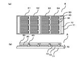
(配線シートに薄膜化合物太陽電池を配置するステップ)
図7は、実施の形態5の薄膜化合物太陽電池アレイを示す図であって、(a)は表面側から見た模式的な平面図と(b)は模式的な断面図である。実施の形態5では、配線シート上に複数の薄膜太陽電池を配置する。図7に示すように、配線シート70上に複数の薄膜太陽電池Sを位置決めして配置する。ここでは、各薄膜太陽電池Sが複数の太陽電池セル(S1,S2)を含むため、効率よく配置することができる。配線シート70は、絶縁性フィルム71と配線72を備える。配線72上に、さらに電極材料73を塗布してもよい。電極材料73としては、銀ペースト等を用いることができ、ディスペンサーやスクリーン印刷等で塗布することができる。配線72は、太陽電池セルの表面電極層と隣接する太陽電池セルの裏面電極とを電気的に接続する。また、薄膜太陽電池の位置決めがしやすいように、配線シートにアライメントマークを入れてもよい。
(Step of placing thin-film compound solar cells on the wiring sheet)
7A and 7B are diagrams showing a thin-film compound solar cell array according to Embodiment 5, wherein FIG. 7A is a schematic plan view viewed from the surface side, and FIG. 7B is a schematic cross-sectional view. In the fifth embodiment, a plurality of thin film solar cells are arranged on a wiring sheet. As shown in FIG. 7, a plurality of thin film solar cells S are positioned and arranged on the wiring sheet 70. Here, since each thin film solar cell S includes a plurality of solar cells (S1, S2), it can be arranged efficiently. The wiring sheet 70 includes an insulating
(配線シートと薄膜化合物太陽電池を接着するステップ)
次に、薄膜太陽電池と配線シート70とを圧着または焼成して、接着させる。銀ペーストは焼成することで硬化し、薄膜太陽電池Sと配線シート70は接着され、電気的にも接続される。
(Step of bonding the wiring sheet and the thin film compound solar cell)
Next, the thin film solar cell and the wiring sheet 70 are bonded to each other by pressure bonding or baking. The silver paste is cured by firing, and the thin film solar cell S and the wiring sheet 70 are bonded and electrically connected.
このように、実施の形態5の薄膜化合物太陽電池アレイの製造方法は、化合物半導体からなる1以上のpn接合を有する太陽電池層と、太陽電池層の受光側に配置された表面電極層と、太陽電池層および表面電極層の受光側を被覆する透明材料とを備え、非受光側において、表面電極層の一部に太陽電池層と透明材料とが配置されない領域を有する薄膜化合物太陽電池の複数を、フィルムの一方の面側に配線を有する配線シート上に配置するステップと、薄膜化合物太陽電池の電極と配線とが電気的に接続されるように配線シートと薄膜化合物太陽電池を接着するステップとを含む。 Thus, the manufacturing method of the thin film compound solar cell array of Embodiment 5 includes a solar cell layer having one or more pn junctions made of a compound semiconductor, a surface electrode layer disposed on the light receiving side of the solar cell layer, A plurality of thin film compound solar cells having a solar cell layer and a transparent material covering the light-receiving side of the surface electrode layer, and having a region where the solar cell layer and the transparent material are not disposed on a part of the surface electrode layer on the non-light-receiving side Are disposed on a wiring sheet having wiring on one surface side of the film, and the step of bonding the wiring sheet and the thin film compound solar cell so that the electrode and the wiring of the thin film compound solar cell are electrically connected to each other Including.
(実施の形態6)
<薄膜化合物太陽電池アレイ>
実施の形態6の薄膜化合物太陽電池アレイは、複数の薄膜化合物太陽電池と、絶縁性フィルムの一方の面側に薄膜化合物太陽電池の電極と電気的に接続された配線を有する配線シートとを備え、薄膜化合物太陽電池は、受光側が透明材料で被覆され、表面電極層の一部に非受光側が太陽電池層および透明樹脂材料で覆われていない開口部を有し、非受光側において、開口部に位置する表面電極層と配線が電気的に接続される。
(Embodiment 6)
<Thin-film compound solar cell array>
The thin film compound solar cell array of Embodiment 6 includes a plurality of thin film compound solar cells and a wiring sheet having wirings electrically connected to the electrodes of the thin film compound solar cells on one surface side of the insulating film. The thin-film compound solar cell has an opening that is coated with a transparent material on the light-receiving side and a non-light-receiving side that is not covered with the solar cell layer and the transparent resin material on a part of the surface electrode layer. The surface electrode layer located in the region and the wiring are electrically connected.
実施の形態6では、実施の形態1の薄膜化合物太陽電池に適用可能な薄膜化合物太陽電池アレイについて説明する。なお、実施の形態6の薄膜化合物太陽電池アレイは、実施の形態2、実施の形態3および実施の形態4の薄膜化合物太陽電池にも適用可能である。
In Embodiment 6, a thin film compound solar cell array applicable to the thin film compound solar cell of
図7は、実施の形態6の薄膜化合物太陽電池アレイを示す図であって、(a)は表面側から見た模式的な平面図と(b)は模式的な断面図である。実施の形態6では、図7に示すように、薄膜化合物太陽電池アレイAは複数の薄膜化合物太陽電池Sと、絶縁性フィルムの一方の面側に薄膜化合物太陽電池の電極と電気的に接続された配線を有する配線シート70とを備える。 7A and 7B are diagrams showing a thin film compound solar cell array according to Embodiment 6, wherein FIG. 7A is a schematic plan view viewed from the surface side, and FIG. 7B is a schematic cross-sectional view. In Embodiment 6, as shown in FIG. 7, the thin film compound solar cell array A is electrically connected to the plurality of thin film compound solar cells S and the electrode of the thin film compound solar cell on one surface side of the insulating film. And a wiring sheet 70 having wiring.
実施の形態6の薄膜化合物太陽電池Sは、図6に示されるように、受光側となる太陽電池層30の上面および表面電極層の上面が透明材料50で被覆されている。一方、非受光側では太陽電池層30の第1コンタクト層41と表面電極層40の一部が露出しており、薄膜化合物太陽電池Sの非受光面側のみでの配線が可能な構成となっている。配線シート70は、絶縁性フィルム71と配線72を備える。配線72上に、さらに電極材料73備えていてもよい。配線72は、薄膜化合物太陽電池の電極と電気的に接続される。
As shown in FIG. 6, in the thin film compound solar cell S of Embodiment 6, the upper surface of the
このように、実施の形態6の薄膜化合物太陽電池アレイは、化合物半導体からなる1以上のpn接合を有する太陽電池層と、太陽電池層の受光側に配置された表面電極層と、太陽電池層および表面電極層の受光側を被覆する透明材料とを備え、非受光側において、表面電極層の一部に太陽電池層と透明材料とが配置されない領域を有する薄膜化合物太陽電池の複数と、フィルムの一方の面側に薄膜化合物太陽電池の電極と電気的に接続された配線を有する配線シートとを備える。 Thus, the thin-film compound solar cell array of Embodiment 6 includes a solar cell layer having one or more pn junctions made of a compound semiconductor, a surface electrode layer disposed on the light receiving side of the solar cell layer, and a solar cell layer. And a plurality of thin-film compound solar cells having a region where the solar cell layer and the transparent material are not disposed on a part of the surface electrode layer on the non-light-receiving side, and a film The wiring sheet which has the wiring electrically connected with the electrode of the thin film compound solar cell is provided in the one surface side.
以上のように本発明の実施の形態および実施例について説明を行なったが、上述の各実施の形態および実施例の構成を適宜組み合わせることも当初から予定している。 Although the embodiments and examples of the present invention have been described as described above, it is also planned from the beginning to appropriately combine the configurations of the above-described embodiments and examples.
今回開示された実施の形態および実施例はすべての点で例示であって制限的なものではないと考えられるべきである。本発明の範囲は上記した説明ではなくて特許請求の範囲によって示され、特許請求の範囲と均等の意味および範囲内でのすべての変更が含まれることが意図される。 It should be understood that the embodiments and examples disclosed herein are illustrative and non-restrictive in every respect. The scope of the present invention is defined by the terms of the claims, rather than the description above, and is intended to include any modifications within the scope and meaning equivalent to the terms of the claims.
10,91,101 基板、20 犠牲層、30,900,1000 太陽電池層、40 表面電極層、50 透明部材、60 開口部、70 配線シート、80,90,100 化合物半導体層、21,102 バッファ層、22,103 犠牲層、23,104 エッチングストップ層、31,93,105 第1コンタクト層、32,94,107 ベース層、33,95,108 エミッタ層、88,96,115 第2コンタクト層、71 フィルム、72 配線、73 電極材料、1100 第1のサブセル、1200 第2のサブセル、R1,R2 太陽電池セル領域、S1,S2,S3,S4 太陽電池セル、S 薄膜化合物太陽電池、A 薄膜化合物太陽電池アレイ。 10, 91, 101 substrate, 20 sacrificial layer, 30, 900, 1000 solar cell layer, 40 surface electrode layer, 50 transparent member, 60 opening, 70 wiring sheet, 80, 90, 100 compound semiconductor layer, 21, 102 buffer Layer, 22, 103 sacrificial layer, 23, 104 etching stop layer, 31, 93, 105 first contact layer, 32, 94, 107 base layer, 33, 95, 108 emitter layer, 88, 96, 115 second contact layer , 71 film, 72 wiring, 73 electrode material, 1100 first subcell, 1200 second subcell, R1, R2 solar cell region, S1, S2, S3, S4 solar cell, S thin film compound solar cell, A thin film Compound solar cell array.
Claims (5)
前記太陽電池層の前記受光面側の表面上に表面電極層を形成するステップと、
前記太陽電池層および前記表面電極層を樹脂を含む透明材料で被覆するステップと、
前記基板を除去するステップと、
前記太陽電池層の一部を除去して表面電極層を前記受光面とは反対側に露出させるステップとをこの順で含む、薄膜化合物太陽電池の製造方法。 Forming a solar cell layer having one or more pn junctions on a substrate in order from a layer located on the side opposite to the light receiving surface by crystal growth;
Forming a surface electrode layer on the light receiving surface side surface of the solar cell layer;
Coating the solar cell layer and the surface electrode layer with a transparent material containing a resin;
Removing the substrate;
A method of manufacturing a thin film compound solar cell , comprising: removing a part of the solar cell layer and exposing a surface electrode layer on the side opposite to the light receiving surface in this order .
前記太陽電池層を形成するステップは、
前記基板上に第1のサブセルを形成するステップと、
前記第1のサブセル上に第2のサブセルを形成するステップを含み、
前記第2のサブセルのバンドギャップは、前記第1のサブセルのバンドギャップよりも大きい、請求項1に記載の薄膜化合物太陽電池の製造方法。 The solar cell layer includes a plurality of subcells having a pn junction,
The step of forming the solar cell layer includes
Forming a first subcell on the substrate;
Forming a second subcell on the first subcell;
2. The method of manufacturing a thin film compound solar cell according to claim 1, wherein a band gap of the second subcell is larger than a bandgap of the first subcell.
前記基板を除去するステップにおいて、前記犠牲層をエッチングすることにより、前記基板を分離する、請求項1または2に記載の薄膜化合物太陽電池の製造方法。 Forming a sacrificial layer by crystal growth between the substrate and the solar cell layer;
The method of manufacturing a thin film compound solar cell according to claim 1 or 2, wherein, in the step of removing the substrate, the substrate is separated by etching the sacrificial layer.
前記基板を除去するステップにおいて、前記基板をエッチング除去する、請求項1または2に記載の薄膜化合物太陽電池の製造方法。 Further comprising the step of crystal growing an etch stop layer between the substrate and the solar cell layer,
The method of manufacturing a thin film compound solar cell according to claim 1 or 2, wherein, in the step of removing the substrate, the substrate is removed by etching.
前記薄膜化合物太陽電池の電極と前記配線とが電気的に接続されるように前記配線シートと前記薄膜化合物太陽電池を接着するステップとを含む、薄膜化合物太陽電池アレイの製造方法。 The manufacturing process of the thin film compound solar cell according to any one of claims 1 to 4, and a step of arranging a plurality of the thin film compound solar cells on a wiring sheet having wiring on one surface side of the film;
The manufacturing method of a thin film compound solar cell array including the step which adhere | attaches the said wiring sheet and the said thin film compound solar cell so that the electrode of the said thin film compound solar cell and the said wiring may be electrically connected.
Priority Applications (1)
| Application Number | Priority Date | Filing Date | Title |
|---|---|---|---|
| JP2015174333A JP6616632B2 (en) | 2015-09-04 | 2015-09-04 | Thin film compound solar cell, thin film compound solar cell manufacturing method, thin film compound solar cell array, and thin film compound solar cell array manufacturing method |
Applications Claiming Priority (1)
| Application Number | Priority Date | Filing Date | Title |
|---|---|---|---|
| JP2015174333A JP6616632B2 (en) | 2015-09-04 | 2015-09-04 | Thin film compound solar cell, thin film compound solar cell manufacturing method, thin film compound solar cell array, and thin film compound solar cell array manufacturing method |
Publications (2)
| Publication Number | Publication Date |
|---|---|
| JP2017050476A JP2017050476A (en) | 2017-03-09 |
| JP6616632B2 true JP6616632B2 (en) | 2019-12-04 |
Family
ID=58280281
Family Applications (1)
| Application Number | Title | Priority Date | Filing Date |
|---|---|---|---|
| JP2015174333A Expired - Fee Related JP6616632B2 (en) | 2015-09-04 | 2015-09-04 | Thin film compound solar cell, thin film compound solar cell manufacturing method, thin film compound solar cell array, and thin film compound solar cell array manufacturing method |
Country Status (1)
| Country | Link |
|---|---|
| JP (1) | JP6616632B2 (en) |
Families Citing this family (1)
| Publication number | Priority date | Publication date | Assignee | Title |
|---|---|---|---|---|
| JP6837877B2 (en) * | 2017-03-14 | 2021-03-03 | シャープ株式会社 | Manufacturing method of solar cell array and solar cell array |
Family Cites Families (3)
| Publication number | Priority date | Publication date | Assignee | Title |
|---|---|---|---|---|
| US5244817A (en) * | 1992-08-03 | 1993-09-14 | Eastman Kodak Company | Method of making backside illuminated image sensors |
| EP2143146A1 (en) * | 2007-04-13 | 2010-01-13 | Semiconductor Energy Laboratory Co, Ltd. | Photovoltaic device and method for manufacturing the same |
| EP2763186A4 (en) * | 2011-12-14 | 2015-01-07 | Panasonic Corp | SOLAR CELL AND METHOD FOR MANUFACTURING THE SAME |
-
2015
- 2015-09-04 JP JP2015174333A patent/JP6616632B2/en not_active Expired - Fee Related
Also Published As
| Publication number | Publication date |
|---|---|
| JP2017050476A (en) | 2017-03-09 |
Similar Documents
| Publication | Publication Date | Title |
|---|---|---|
| TWI660520B (en) | Integration of epitaxial lift-off solar cells with mini-parabolic concentrator arrays via printing method | |
| US8823127B2 (en) | Multijunction photovoltaic cell fabrication | |
| CN110246919A (en) | Photovoltaic module and its manufacturing process comprising lapping photovoltaic tiles | |
| JP5414010B2 (en) | Multi-junction compound solar cell, multi-junction compound solar cell, and method for producing the same | |
| JP2010245176A (en) | Method for manufacturing solar cell sheet array and solar cell sheet array | |
| US20180233612A1 (en) | Thin-film compound photovoltaic cell, method for manufacturing thin-film compound photovoltaic cell, thin-film compound photovoltaic cell array, and method for manufacturing thin-film compound photovoltaic cell array | |
| JP5273728B2 (en) | Solar cell with wiring sheet and solar cell module | |
| WO2007015354A1 (en) | Method for manufacturing photoelectric converter and photoelectric converter | |
| CN102956552A (en) | Preparation method for semiconductor device | |
| CN108269864B (en) | A kind of flexible solar cell and preparation method thereof | |
| EP3258502B1 (en) | Solar cell module | |
| CN108231934A (en) | A kind of solar cell module and preparation method thereof | |
| JP6616632B2 (en) | Thin film compound solar cell, thin film compound solar cell manufacturing method, thin film compound solar cell array, and thin film compound solar cell array manufacturing method | |
| JP4974545B2 (en) | Method for manufacturing solar cell string | |
| JP4245135B2 (en) | Thin film solar cell manufacturing method | |
| CN120018690A (en) | Perovskite tandem solar cell and preparation method thereof | |
| CN108231936A (en) | A kind of solar cell module and preparation method thereof | |
| JP4245131B2 (en) | Method for manufacturing thin film solar cell | |
| TWI496308B (en) | Thin film solar cell and manufacturing method thereof | |
| JP2014103305A (en) | Solar cell element and method of manufacturing the same | |
| CN115763579A (en) | Solar cell and preparation method thereof | |
| CN224037763U (en) | Perovskite tandem solar cells | |
| CN111628022A (en) | GaAs-based photoelectric device and preparation method of array thereof | |
| JP4762753B2 (en) | Method for producing thin film single crystal compound solar cell | |
| JP3766248B2 (en) | Manufacturing method of solar cell module |
Legal Events
| Date | Code | Title | Description |
|---|---|---|---|
| RD02 | Notification of acceptance of power of attorney |
Free format text: JAPANESE INTERMEDIATE CODE: A7422 Effective date: 20161104 |
|
| A621 | Written request for application examination |
Free format text: JAPANESE INTERMEDIATE CODE: A621 Effective date: 20180323 |
|
| A131 | Notification of reasons for refusal |
Free format text: JAPANESE INTERMEDIATE CODE: A131 Effective date: 20181002 |
|
| A977 | Report on retrieval |
Free format text: JAPANESE INTERMEDIATE CODE: A971007 Effective date: 20180928 |
|
| A521 | Request for written amendment filed |
Free format text: JAPANESE INTERMEDIATE CODE: A523 Effective date: 20181130 |
|
| A131 | Notification of reasons for refusal |
Free format text: JAPANESE INTERMEDIATE CODE: A131 Effective date: 20190205 |
|
| A521 | Request for written amendment filed |
Free format text: JAPANESE INTERMEDIATE CODE: A523 Effective date: 20190405 |
|
| A02 | Decision of refusal |
Free format text: JAPANESE INTERMEDIATE CODE: A02 Effective date: 20190514 |
|
| A521 | Request for written amendment filed |
Free format text: JAPANESE INTERMEDIATE CODE: A523 Effective date: 20190806 |
|
| A911 | Transfer to examiner for re-examination before appeal (zenchi) |
Free format text: JAPANESE INTERMEDIATE CODE: A911 Effective date: 20190814 |
|
| TRDD | Decision of grant or rejection written | ||
| A01 | Written decision to grant a patent or to grant a registration (utility model) |
Free format text: JAPANESE INTERMEDIATE CODE: A01 Effective date: 20191015 |
|
| A61 | First payment of annual fees (during grant procedure) |
Free format text: JAPANESE INTERMEDIATE CODE: A61 Effective date: 20191108 |
|
| R150 | Certificate of patent or registration of utility model |
Ref document number: 6616632 Country of ref document: JP Free format text: JAPANESE INTERMEDIATE CODE: R150 |
|
| LAPS | Cancellation because of no payment of annual fees |