CN100504709C - Overcurrent detecting circuit and regulator having the same - Google Patents
Overcurrent detecting circuit and regulator having the same Download PDFInfo
- Publication number
- CN100504709C CN100504709C CNB2005800029850A CN200580002985A CN100504709C CN 100504709 C CN100504709 C CN 100504709C CN B2005800029850 A CNB2005800029850 A CN B2005800029850A CN 200580002985 A CN200580002985 A CN 200580002985A CN 100504709 C CN100504709 C CN 100504709C
- Authority
- CN
- China
- Prior art keywords
- transistor
- output
- current
- voltage
- sensing circuit
- Prior art date
- Legal status (The legal status is an assumption and is not a legal conclusion. Google has not performed a legal analysis and makes no representation as to the accuracy of the status listed.)
- Expired - Fee Related
Links
Images


Classifications
-
- G—PHYSICS
- G05—CONTROLLING; REGULATING
- G05F—SYSTEMS FOR REGULATING ELECTRIC OR MAGNETIC VARIABLES
- G05F1/00—Automatic systems in which deviations of an electric quantity from one or more predetermined values are detected at the output of the system and fed back to a device within the system to restore the detected quantity to its predetermined value or values, i.e. retroactive systems
- G05F1/10—Regulating voltage or current
- G05F1/46—Regulating voltage or current wherein the variable actually regulated by the final control device is dc
- G05F1/56—Regulating voltage or current wherein the variable actually regulated by the final control device is dc using semiconductor devices in series with the load as final control devices
- G05F1/565—Regulating voltage or current wherein the variable actually regulated by the final control device is dc using semiconductor devices in series with the load as final control devices sensing a condition of the system or its load in addition to means responsive to deviations in the output of the system, e.g. current, voltage, power factor
- G05F1/569—Regulating voltage or current wherein the variable actually regulated by the final control device is dc using semiconductor devices in series with the load as final control devices sensing a condition of the system or its load in addition to means responsive to deviations in the output of the system, e.g. current, voltage, power factor for protection
- G05F1/573—Regulating voltage or current wherein the variable actually regulated by the final control device is dc using semiconductor devices in series with the load as final control devices sensing a condition of the system or its load in addition to means responsive to deviations in the output of the system, e.g. current, voltage, power factor for protection with overcurrent detector
-
- G—PHYSICS
- G05—CONTROLLING; REGULATING
- G05F—SYSTEMS FOR REGULATING ELECTRIC OR MAGNETIC VARIABLES
- G05F1/00—Automatic systems in which deviations of an electric quantity from one or more predetermined values are detected at the output of the system and fed back to a device within the system to restore the detected quantity to its predetermined value or values, i.e. retroactive systems
- G05F1/10—Regulating voltage or current
- G05F1/46—Regulating voltage or current wherein the variable actually regulated by the final control device is dc
- G05F1/56—Regulating voltage or current wherein the variable actually regulated by the final control device is dc using semiconductor devices in series with the load as final control devices
-
- G—PHYSICS
- G05—CONTROLLING; REGULATING
- G05F—SYSTEMS FOR REGULATING ELECTRIC OR MAGNETIC VARIABLES
- G05F1/00—Automatic systems in which deviations of an electric quantity from one or more predetermined values are detected at the output of the system and fed back to a device within the system to restore the detected quantity to its predetermined value or values, i.e. retroactive systems
- G05F1/10—Regulating voltage or current
-
- H—ELECTRICITY
- H02—GENERATION; CONVERSION OR DISTRIBUTION OF ELECTRIC POWER
- H02H—EMERGENCY PROTECTIVE CIRCUIT ARRANGEMENTS
- H02H3/00—Emergency protective circuit arrangements for automatic disconnection directly responsive to an undesired change from normal electric working condition with or without subsequent reconnection ; integrated protection
- H02H3/08—Emergency protective circuit arrangements for automatic disconnection directly responsive to an undesired change from normal electric working condition with or without subsequent reconnection ; integrated protection responsive to excess current
- H02H3/087—Emergency protective circuit arrangements for automatic disconnection directly responsive to an undesired change from normal electric working condition with or without subsequent reconnection ; integrated protection responsive to excess current for dc applications
Abstract
The present invention provides an overcurrent detection circuit capable of suppressing fluctuations in the overcurrent detection level when the input supply voltage or temperature fluctuates. The overcurrent detection circuit 10b comprises a monitor transistor 21 a control terminal and output terminal of which are connected to a control terminal and output terminal respectively of an output transistor 11; an output current detection transistor 22b to a control terminal of which a detection bias voltage 28 is input, and an output terminal of which is connected to an input terminal of the monitor transistor 21; a constant current source 24 that generates a reference current I REF ; a reference transistor 23 to a control terminal of which the detection bias voltage 28 is input and from the output terminal of which the reference current I REF flows to the constant current source 24; and a comparison circuit 25b that outputs an overcurrent detection signal by comparing the voltage of the output terminal of the output current detection transistor 22b and the voltage of the output terminal of the reference transistor 23.
Description
Technical field
The present invention relates to a kind of for example in supply voltage being transformed into the regulator (regulator) of given dc voltage under the situation as circulation excess current in the output transistor of the inscape of load output current, the regulator that detects this excess current and the overcurrent sensing circuit of protecting and have this overcurrent sensing circuit.
Background technology
Regulator such as switching regulaor and series controller is connected with input supply voltage and load, is provided with output transistor between the terminal of the given dc voltage of output, keeps given dc voltage by controlling this output transistor.Afterwards, when the situation of load short circuits etc. is unusual, destroy because of excess current, need to be provided with the circuit (for example patent documentation 1) that detects excess current and protect in order to prevent output transistor.
Overcurrent sensing circuit before having illustrated among Fig. 4 and regulator with this circuit.This regulator 101 have the output transistor 11 that adopts P type MOS transistor, with the smoothing circuit 12 of the output smoothingization of output transistor 11, output smoothing change given dc voltage lead-out terminal OUT, with Voltage Feedback input and the control circuit 14 of control output transistor 11 and the overcurrent sensing circuit 110a that detects the excess current of output transistor 11 and protect of lead-out terminal OUT.Lead-out terminal OUT is connected with load 13.
Now, if circulate output current I in the output transistor 11
0, then monitor with about I that just circulates in the transistor 121
0The electric current of/N, correspondent voltage are benchmark with the earthing potential, are created in the output current detection resistance 122.Like this, output current I
0Become excess current, if this voltage has surpassed the threshold value (Vth) of excess current detection output transistor 123, just excess current detects output transistor 123 output low levels.By like this, control circuit 14 thinks that the output current of output transistor 11 has surpassed excess current detection level (judging the circulation excess current), by output transistor 11.Here, the excess current detection level can be adjusted with the size of transistor 121 and the resistance value of output current detection resistance 122 by monitoring.
Next, another overcurrent sensing circuit before having and the regulator with this circuit have been shown among Fig. 5.This regulator 102 is except overcurrent sensing circuit 110b, all the formation with above-mentioned regulator 101 is identical in fact, overcurrent sensing circuit 110b is also the same with above-mentioned overcurrent sensing circuit 110a, has monitoring and hinders 122 with transistor 121 and output current detection.In addition, overcurrent sensing circuit 110b has excess current and detects output with comparer 125, replaces excess current to detect output transistor 123.This excess current detects output comparer 125, reversed input terminal is connected with the contact of transistor 121 with output current detection resistance 122 with monitoring, in-phase input terminal detects with excess current and is connected with reference voltage 124, and lead-out terminal is connected with control circuit 14.
Wherein too, if circulate output current I in the output transistor 11
0, monitoring about I that just circulates in the transistor 121
0The electric current of/N, correspondent voltage are benchmark with the earthing potential, are created in the output current detection resistance 122.Like this, output current I
0Become excess current, detect with reference voltage 124, just excess current detects output comparer 125 output low levels if this voltage has surpassed excess current.By like this, control circuit 14 thinks that the output current of output transistor 11 has surpassed the excess current detection level, by output transistor 11.Here, the excess current detection level can be adjusted with the value of reference voltage 124 with the size of transistor 121, the resistance value and the excess current detection of output current detection resistance 122 by monitoring.
Patent documentation 1: the spy opens flat 8-No. 331757 communiques
Like this, overcurrent sensing circuit 110a and 110b can detect the excess current of circulation in the output transistor 11.But, the inventor that the further high precision int of the excess current detection level of overcurrent sensing circuit is studied notices, in this overcurrent sensing circuit 110a and 110b, the voltage that is produced in the output current detection resistance 122, also i.e. monitoring is benchmark with the ground voltage with the drain voltage of transistor 121, and the drain voltage of output transistor 11 is not benchmark with the earthing potential.By like this, monitor and use the drain voltage of transistor 121 different with the drain voltage of output transistor 11, its result can envision the electric current of monitoring with transistor 121 and depart from I
0The value of/N.
Therefore, the someone considers to precompute this deviation, the resistance value of change output current detection resistance 122, adjust the excess current detection level, but taken place in the power source voltage Vcc of being imported under the situation of change, the degree of deviation also can change, so this countermeasure does not have effect.
In addition, the inventor also once was conceived to when change has taken place temperature, because of monitoring uses the temperature characterisitic of transistor 11 and output current detection resistance 122 different with transistor 121 and output, to the influence of excess current detection level.In addition, among the overcurrent sensing circuit 110a, excess current detects the also change of characteristic of output transistor 123, therefore can envision the further change of excess current detection level.
Summary of the invention
The present invention is in view of above problem, and purpose is to provide a kind of overcurrent sensing circuit that can be suppressed at the change of the excess current detection level under the situation that change has taken place the supply voltage imported or temperature, and the regulator with it.
In order to address the above problem, the relevant overcurrent sensing circuit of desirable embodiment of the present invention, be transfused to supply voltage at input end, control end is transfused to control voltage, from the output transistor of output terminal output output current, when circulation has excess current, it is detected, this overcurrent sensing circuit has: the monitoring transistor that control end and output terminal are connected with the control end and the output terminal of output transistor respectively; Input end is transfused to supply voltage, and control end is transfused to detect uses bias voltage, and output terminal detects with the output current that monitoring is connected with transistorized input end and uses transistor; Generate the constant current source of reference current; Input end is transfused to supply voltage, and control end is transfused to detect uses bias voltage, from the reference transistor of output terminal to above-mentioned constant current source circulation said reference electric current; And by output current being detected voltage with transistorized output terminal, compare with the voltage of reference with transistorized output terminal, circulation is when having excess current in output transistor, it detected and exports the comparator circuit that is made of comparer of over-current detection signal.
Above-mentioned output transistor, above-mentioned monitoring detect with transistor and above-mentioned with reference to using transistor, preferably P type MOS transistor with transistor, above-mentioned output current.
Above-mentioned comparator circuit preferably has: being situated between is inserted in above-mentioned constant current source and reference and the 1st relatively uses transistor with what the diode between the transistor was connected; Generate the 2nd constant current source of given times of electric current of the reference current that above-mentioned constant current source generates; And be situated between and be inserted in the 2nd constant current source and detect between the usefulness transistor with output current, control end relatively the 2nd is relatively used transistor with what transistorized control end was connected with the 1st.
The associated adjustment device of desirable embodiment of the present invention, it is regulator with above-mentioned overcurrent sensing circuit, be provided with control circuit, it is provided with output transistor between the lead-out terminal of supply voltage and the given dc voltage of output, the Voltage Feedback of lead-out terminal is imported, and the output transistor that should keep given dc voltage is controlled, simultaneously, in case be transfused to the over-current detection signal of overcurrent sensing circuit, just by output transistor.
The invention effect
The relevant overcurrent sensing circuit of desirable embodiment of the present invention, to monitor and detect in parallel with output transistor with transistorized concatermer with the transistor AND gate output current, and will use the transistor parallel connection with reference to detecting with the transistor AND gate output current, by being detected with transistorized output and reference, output current compares with transistorized output, detect excess current, even therefore supply voltage or the temperature of being imported changes, this characteristics of transistor does not have any change comparatively speaking yet, therefore can suppress the change of excess current detection level.In addition, have its regulator,, therefore can improve fiduciary level because the excess current detection level is stable.
Description of drawings
Fig. 1 is the relevant overcurrent sensing circuit of embodiments of the present invention and the circuit diagram with its regulator.
Fig. 2 is a movement oscillogram as above.
Fig. 3 is relevant overcurrent sensing circuit of another embodiment of the present invention and the circuit diagram with its regulator.
Fig. 4 is the overcurrent sensing circuit of background technology and the circuit diagram with its regulator.
Fig. 5 is another overcurrent sensing circuit of background technology and the circuit diagram with its regulator.
Among the figure: 1,2-regulator, 10a, 10b-overcurrent sensing circuit, 11-output transistor, 13-load, 21-monitoring transistor, 22a, 22b-output current detect uses transistor, 23-with reference to using transistor, 24-constant current source, 25a, 25b-comparator circuit, 28-detect and use bias voltage, 31-the 1 relatively uses transistor, and 32-the 2 relatively uses transistor, 33-the 2 constant current source, the supply voltage of Vcc-input, the lead-out terminal of OUT-regulator.
Embodiment
The contrast accompanying drawing describes preferred forms of the present invention below.Fig. 1 is the overcurrent sensing circuit of embodiments of the present invention and the circuit diagram with its regulator.This regulator 1 is provided with the output transistor 11 that adopts P type MOS transistor between power source voltage Vcc and lead-out terminal OUT, by control output transistor 11 lead-out terminal OUT is maintained given dc voltage, simultaneously, in output transistor 11 under the situation of circulation excess current, overcurrent sensing circuit 10a detects it and by output transistor 11.In more detail, this regulator 1 has: input end (source electrode) is transfused to power source voltage Vcc, and control end (grid) is transfused to control voltage, from output terminal (drain electrode) output output current I
0Output transistor 11; Allow the smoothing circuit 12 of the voltage smoothing that output terminal produced of output transistor 11; The output smoothing change the lead-out terminal OUT of given dc voltage; The voltage of feedback input and output terminal OUT and the control of the node C from the Fig. 1 that should keep given dc voltage output transistor 11, if be transfused to the over-current detection signal of overcurrent sensing circuit 10a simultaneously from node D, just should end the control circuit 14 that the control voltage of the node C of output transistor 11 is made as the power source voltage Vcc level; And under the situation of the excess current that in output transistor 11, circulates it is detected, this over-current detection signal is exported to the overcurrent sensing circuit 10a of control circuit 14 from node D.Lead-out terminal OUT is connected with load 13.
Overcurrent sensing circuit 10a has: the monitoring of the employing P type MOS transistor that control end (grid) and output terminal (drain electrode) are connected with the control end (grid) and the output terminal (drain electrode) of output transistor 11 respectively transistor 21; Input end (source electrode) is transfused to power source voltage Vcc, control end (grid) is transfused to and detects with biasing (bias) voltage 28, the output current detection transistor 22a of the employing P type MOS transistor that output terminal (drain electrode) is connected with the input end of monitoring with transistor 21 (source electrode); Generate reference current I
REFThe constant current source 24 of the employing N type MOS transistor of (for example 10 μ A); Input end (source electrode) is transfused to power source voltage Vcc, and control end (grid) is transfused to and detects with bias voltage 28, and from output terminal (drain electrode) to the constant current source 24 reference current I that circulate
REFThe reference of employing P type MOS transistor with transistor 23; And output current detected with the voltage (also being the voltage of the Node B among Fig. 1) of the output terminal (drain electrode) of transistor 22a and the reference voltage (also being the voltage of the node A among Fig. 1) with the output terminal (drain electrode) of transistor 23 compare, node D output detection signal by comparator circuit 25a that comparer constituted.This comparator circuit 25a, more specifically, during the excess current that do not circulate in output transistor 11, the detection signal of output high level detects the also over-current detection signal of output low level with it when the circulation excess current.Also be, overcurrent sensing circuit 10a, monitoring is arranged in parallel with transistor 21 and concatermer and the output transistor 11 that output current detects with transistor 22a, and will be arranged in parallel with transistor 22a with reference to detecting with output current with transistor 23, compare with the output of transistor 23 with reference by output current being detected, detect excess current with the output of transistor 22a.In addition, monitoring detects with transistor 22a and with reference to the equal and opposite in direction with transistor 23 with transistor 21, output current, and is made as the 1/N (for example 1/50000) of the size of output transistor 11.In addition, overcurrent sensing circuit 10a also has N type MOS transistor 26 and constant current source 27, by the current value of their decision constant current sources 24.
In addition, input to the detection bias voltage 28 that output current detects the control end of using transistor 22a and reference to use transistor 23 simultaneously, preferably almost consistent with the voltage of monitoring the control end (grid) of using transistor 21.For example, be under the situation of switching regulaor at regulator 1, detect and use preferably ground voltage level of bias voltage 28.
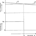
Next, the action to overcurrent sensing circuit 10a describes according to the movement oscillogram of Fig. 2.This action waveforms illustrates the action waveforms (curve A and curve B) of node A and B, also is node A and the relative output current I of voltage of B
0Variation, and the action waveforms of comparator circuit 25a also is the variation of detection signal output (voltage of node D).Owing to monitoring detects the 1/N that is set to output transistor 11 with the size of transistor 22a with transistor 21 and output current, if so output current I that circulates in the output transistor 11
0, (concatermer) monitoring of series connection detects with the electric current I that is circulated among the transistor 22a with transistor 21 and output current
1Just become about I
0/ 2N.Also promptly, be R if establish monitoring with the value that transistor 21 and output current detect with the resistance of equal value of transistor 22a, then the value owing to the resistance of equal value of output transistor 11 is R/N, so sets up following formula.
RI
1+RI
1=RI
0/N …(1)
Therefore,
I
1=I
0/2N …(2)
Like this, in the Node B, for the I that circulates in detecting with transistor 22a at output current
0The electric current of/2N, and be that benchmark has produced necessary voltage with the power source voltage Vcc.In case the voltage of Node B is the output current I of output transistor 11
0Increasing just, straight line descends.In addition, among the node A, in order to use circulation reference current I in the transistor 23 in reference
REF, and be that benchmark produces necessary voltage with the power source voltage Vcc.Therefore, the output current I of output transistor 11
0Increase, in case monitoring detects with the electric current I that is circulated among the transistor 22a with transistor 21 and output current
0/ 2N surpasses reference current I
REFValue, also be that the voltage of Node B drops to below the voltage of node A, the detection signal of the node D of the output of circuit 25a just is changed to low level (over-current detection signal) from high level as a comparison.Specifically, if N is made as 50000, with reference current I
REFBe made as 10 μ A, then the electric current I of output transistor 11
0Just be about more than the 1A (ampere), think the output current I of output transistor 11
0Surpassed excess current detection level I
E(judging that circulation has excess current) ends output transistor 11.
Here, the monitoring of concatermer detects with output current with transistor 21 and uses transistor 22a, and reference is the same with output transistor 11 with the voltage of each output terminal (drain electrode) of transistor 23, corresponding to the value of the electric current that is circulated, be that benchmark generates with the power source voltage Vcc.Therefore, the voltage of these transistorized output terminals (drain electrode) changes because of the influence of other elements, departs from the ratio of size by such ratio that has suppressed the electric current that wherein circulated.Like this,, generate, therefore not influenced by it, almost do not cause excess current detection level I because the voltage of above-mentioned transistorized output terminal (drain electrode) is benchmark with the power source voltage Vcc even taken place in power source voltage Vcc under the situation of change
EChange.
In addition, output transistor 11, monitoring detect with transistor 22a and with reference to transistor 23 with transistor 21, output current, are P type MOS transistor, therefore have identical temperature characterisitic.Therefore, monitoring detects with transistor 22a and with reference to the characteristic with transistor 23 with transistor 21, output current, even temperature change also changes equally with output transistor 11, therefore can suppress the caused excess current detection level of the change I of Yin Wendu
EChange.
Next, according to Fig. 3 the overcurrent sensing circuit of another embodiment of the present invention and regulator with it are described.This regulator 2 is except overcurrent sensing circuit 10b, and all the formation with above-mentioned regulator 1 is identical in fact, therefore following overcurrent sensing circuit 10b is described.
In addition, overcurrent sensing circuit 10b replaces to the comparator circuit 25b with other circuit structures with the comparator circuit 25a that comparer constituted in the previous embodiment.Comparator circuit 25b has: being situated between is inserted in constant current source 24 and relatively uses transistor 31 with reference to the 1st of the employing P type MOS transistor that is connected (output terminal (drain electrode) is connected with control end (grid)) with the diode between the transistor 23; Constant current source (N type MOS transistor) 24 and grid voltage are common to generate the reference current I that constant current source 24 is generated by allowing
REFThe 2nd constant current source 33 of electric current of given times (being 1 times here); And be situated between and be inserted in the 2nd constant current source 33 and detect between the usefulness transistor 22b with output current, control end (grid) and the 1st relatively uses the 2nd of employing P type MOS transistor that the control end (grid) of transistor 31 is connected relatively to use transistor 32.Therefore, if the 2nd relatively use the current potential of the input end (source electrode) of transistor 32 relatively to use the input end (source electrode) of transistor 31 low than the 1st, just the 2nd relatively use in the transistor 32 not circulating current (ending) with descending.
Next, the action to overcurrent sensing circuit 10b describes.If establish monitoring with transistor 21 be R with reference to value with the resistance of equal value of transistor 23, then the output current detection is R/2 with the value of the resistance of equal value of transistor 22b, the value of the resistance of equal value of output transistor 11 is R/N.Output current detects with the electric current that is circulated among the transistor 22b, along separate routes for monitoring with the electric current I that is circulated in the transistor 21
1With the electric current I that is circulated in the 2nd constant current source 33
REFTherefore, in the Node B, for circulating current I in detecting with transistor 22b at output current
REF+ I
1, and be that benchmark generates necessary voltage R (I with the power source voltage Vcc
REF+ I
1)/2.So:
R(I
REF+I
1)/2+RI
1=RI
0/N …(3)
Set up, for satisfying following formula at monitoring circulating current I in the transistor 21
1
In addition, among the node A, in order to allow with reference to using circulation reference current I in the transistor 23
REF, and be that benchmark has generated necessary voltage RI with the power source voltage Vcc
REFIf the voltage of Node B equates with the voltage of node A, then
R(I
REF+I
1)/2=R
IREF …(4)
Set up.Find the solution just and obtain:
I
1=I
REF …(5)
Formula (5) substitution formula (3) is just obtained:
I
1=I
REF=I
0/2N …(6)
Like this, if monitoring has surpassed electric current I with the electric current I 1 that is circulated in the transistor 21
REF, then since the voltage of Node B drop to node A below, therefore the 2nd relatively ends with transistor 32, the output of comparator circuit 25b also is that the detection signal of node D becomes low level (over-current detection signal) from high level.Specifically, be 50000 if establish N, reference current I
REFBe 10 μ A, the output current I of output transistor 11 then
0More than 1A, the detection signal of node D becomes low level.
Like this, overcurrent sensing circuit 10b is the same with overcurrent sensing circuit 10a, and circulating in output transistor 11 has under the situation of excess current, it is detected and over-current detection signal is exported to control circuit 14 from node D.In addition,, therefore can cut down the parts number of forming circuit, reduce occupied area and consumed power because the comparator circuit 25b of this overcurrent sensing circuit 10b does not use the comparer as the comparator circuit 25a of overcurrent sensing circuit 10a.
In addition, among overcurrent sensing circuit 10a or the 10b, also can be in order to adjust excess current detection level I
EAnd change reference current I
REFIn addition, among the overcurrent sensing circuit 10b, can also by with the size of the 2nd constant current source (N type MOS transistor) 33 relatively constant current source (N type MOS transistor) thus the given multiplying power of the current value that 24 changes are circulated, to excess current detection level I
EAdjust.For example, be 1/2 if establish the size of the 2nd constant current source (N type MOS transistor) 33, then because;
I
REF=2I
0/5N …(7)
Make the voltage of Node B equate with the voltage of node A.Therefore, be 50000 if establish N, reference current I
REFBe 10 μ A, then excess current detection level I
EBecome 1.25A.
In addition, can also adjust excess current detection level I by changing with reference to monitoring the size ratio that detects with transistor 22a (22b) with transistor 21 and output current relatively with transistor 23
EFor example, among the overcurrent sensing circuit 10a, detect with 1/2 of transistor 22a with transistor 21 and output current with reference to be of a size of monitoring with transistor 23 if allow, (N is 50000, reference current I then under these conditions
REFBe 10 μ A), excess current detection level I
EBecome 2A.In addition, among the overcurrent sensing circuit 10b, if allow with reference to transistor 23 be of a size of the monitoring with transistor 21 1/2, then because of:
I
REF=I
0/5N …(8)
Make the voltage of Node B equate with the voltage of node A.Therefore, (N is 50000, reference current I under these conditions
REFBe 10 μ A), excess current detection level I
EBecome 2.5A.
In addition, the present invention is not limited in above-mentioned embodiment, can also carry out various design alterations in the scope of the described item of claim.For example, in the above-mentioned embodiment, the output transistor 11 of illustrated is regulator is P type MOS transistor, the monitoring of overcurrent sensing circuit transistor 21, output current detects with transistor 22a (22b) and with reference to being P type MOS transistor with transistor 23, but output transistor 11 can also adopt N type MOS transistor, positive-negative-positive bipolar transistor or bipolar npn transistor, in this case, monitor certainly with transistor 21, output current detects with transistor 22a (22b) and with reference to constituting overcurrent sensing circuit by corresponding the above-mentioned type with transistor 23.
Claims (4)
1. an overcurrent sensing circuit is transfused to supply voltage at input end, and control end is transfused to control voltage, from the output transistor of output terminal output output current, when circulation has excess current, it is detected,
Described overcurrent sensing circuit has:
The monitoring transistor that control end and output terminal are connected with the control end and the output terminal of output transistor respectively;
Input end is transfused to supply voltage, and control end is transfused to detect uses bias voltage, and output terminal detects with the output current that monitoring is connected with transistorized input end and uses transistor;
Generate the constant current source of reference current;
Input end is transfused to supply voltage, and control end is transfused to detect uses bias voltage, flows into the reference transistor of described reference current to described constant current source from output terminal; And
By output current being detected voltage with transistorized output terminal, compare with the voltage of reference with transistorized output terminal, circulation is when having excess current in output transistor, it detected and exports the comparator circuit that is made of comparer of over-current detection signal.
2. overcurrent sensing circuit as claimed in claim 1 is characterized in that,
It is P type MOS transistor with transistor that described output transistor, described monitoring detect with transistor and described reference with transistor, described output current.
3. overcurrent sensing circuit as claimed in claim 1 or 2 is characterized in that,
To be replaced to the comparator circuit with following structure by the comparator circuit that comparer constitutes: being situated between is inserted in described constant current source and reference and the 1st relatively uses transistor with what the diode between the transistor was connected; Generate the 2nd constant current source of given times of electric current of the reference current that described constant current source generates; And be situated between and be inserted in the 2nd constant current source and detect between the usefulness transistor with output current, control end relatively the 2nd is relatively used transistor with what transistorized control end was connected with the 1st.
4. a regulator has each described overcurrent sensing circuit in the claim 1~3, it is characterized in that,
Be provided with control circuit, it is provided with output transistor between the lead-out terminal of supply voltage and the given dc voltage of output, Voltage Feedback input with lead-out terminal, and the output transistor that should keep given dc voltage controlled, simultaneously, in case be transfused to the over-current detection signal of overcurrent sensing circuit, just by output transistor.
Applications Claiming Priority (2)
| Application Number | Priority Date | Filing Date | Title |
|---|---|---|---|
| JP2004014988A JP3889402B2 (en) | 2004-01-22 | 2004-01-22 | Overcurrent detection circuit and regulator provided with the same |
| JP014988/2004 | 2004-01-22 |
Publications (2)
| Publication Number | Publication Date |
|---|---|
| CN1910529A CN1910529A (en) | 2007-02-07 |
| CN100504709C true CN100504709C (en) | 2009-06-24 |
Family
ID=34805442
Family Applications (1)
| Application Number | Title | Priority Date | Filing Date |
|---|---|---|---|
| CNB2005800029850A Expired - Fee Related CN100504709C (en) | 2004-01-22 | 2005-01-19 | Overcurrent detecting circuit and regulator having the same |
Country Status (7)
| Country | Link |
|---|---|
| US (1) | US7573689B2 (en) |
| EP (1) | EP1708069A4 (en) |
| JP (1) | JP3889402B2 (en) |
| KR (1) | KR20060127070A (en) |
| CN (1) | CN100504709C (en) |
| TW (1) | TW200601658A (en) |
| WO (1) | WO2005071511A1 (en) |
Cited By (2)
| Publication number | Priority date | Publication date | Assignee | Title |
|---|---|---|---|---|
| CN102270828A (en) * | 2010-06-07 | 2011-12-07 | 罗姆股份有限公司 | Load driving device and electrical apparatus using same |
| CN102594109A (en) * | 2011-01-05 | 2012-07-18 | 上海华虹集成电路有限责任公司 | Current-limiting comparison circuit |
Families Citing this family (25)
| Publication number | Priority date | Publication date | Assignee | Title |
|---|---|---|---|---|
| US7532448B2 (en) * | 2006-10-13 | 2009-05-12 | Advanced Analogic Technologies, Inc. | Current limit detector |
| US7957116B2 (en) | 2006-10-13 | 2011-06-07 | Advanced Analogic Technologies, Inc. | System and method for detection of multiple current limits |
| US7672107B2 (en) * | 2006-10-13 | 2010-03-02 | Advanced Analogic Technologies, Inc. | Current limit control with current limit detector |
| JP4996203B2 (en) * | 2006-11-07 | 2012-08-08 | ルネサスエレクトロニクス株式会社 | Power supply voltage circuit |
| CN101247212B (en) * | 2007-02-14 | 2012-06-20 | 中芯国际集成电路制造(上海)有限公司 | Data detection circuit |
| JP4953246B2 (en) * | 2007-04-27 | 2012-06-13 | セイコーインスツル株式会社 | Voltage regulator |
| CN101188413B (en) * | 2007-11-30 | 2010-05-26 | 艾默生网络能源有限公司 | An input simulation detection circuit for frequency converter |
| JP5310023B2 (en) * | 2009-01-23 | 2013-10-09 | ミツミ電機株式会社 | Semiconductor integrated circuit for regulator |
| US8325453B2 (en) * | 2009-05-28 | 2012-12-04 | Qualcomm, Incorporated | Short-circuit protection for switched output stages |
| JP5285644B2 (en) * | 2010-03-26 | 2013-09-11 | 旭化成エレクトロニクス株式会社 | Overcurrent protection circuit, switching regulator, switching amplifier |
| TWI448870B (en) * | 2010-08-25 | 2014-08-11 | Hon Hai Prec Ind Co Ltd | Regulator circuit structure |
| US8816722B2 (en) * | 2010-09-13 | 2014-08-26 | Semiconductor Energy Laboratory Co., Ltd. | Current detection circuit |
| US8890579B2 (en) * | 2012-07-20 | 2014-11-18 | Texas Instruments Incorporated | Circuit for current sensing in high-voltage transistor |
| US10041982B2 (en) * | 2012-08-15 | 2018-08-07 | Texas Instruments Incorporated | Switch mode power converter current sensing apparatus and method |
| JP6205142B2 (en) * | 2013-03-08 | 2017-09-27 | エスアイアイ・セミコンダクタ株式会社 | Constant voltage circuit |
| JP6302639B2 (en) * | 2013-10-08 | 2018-03-28 | ローム株式会社 | Current monitoring circuit |
| JP6354720B2 (en) | 2015-09-25 | 2018-07-11 | 株式会社デンソー | Regulator circuit with protection circuit |
| US11239837B2 (en) | 2017-12-15 | 2022-02-01 | Rohm Co., Ltd. | Switch device |
| JP7149104B2 (en) | 2018-05-28 | 2022-10-06 | ローム株式会社 | Semiconductor integrated circuits, audio output devices, electronic equipment |
| US11251729B2 (en) | 2018-07-02 | 2022-02-15 | Infinno Technology Corp. | Device and method for over-current protection |
| CN110401168B (en) * | 2019-08-22 | 2022-02-11 | 广东美的制冷设备有限公司 | Anti-interference circuit and air conditioner |
| KR20210051388A (en) * | 2019-10-30 | 2021-05-10 | 삼성전자주식회사 | Protection circuit in a electronic device and therfor method |
| US11539393B2 (en) * | 2020-08-07 | 2022-12-27 | Apple Inc. | Radio-frequency front end modules with leakage management engines |
| CN113884208B (en) * | 2021-09-09 | 2023-10-10 | 芯原微电子(成都)有限公司 | High-precision over-temperature detection circuit |
| CN116609643B (en) * | 2023-07-21 | 2023-09-19 | 江苏兴宙微电子有限公司 | Signal detection circuit and integrated circuit |
Family Cites Families (12)
| Publication number | Priority date | Publication date | Assignee | Title |
|---|---|---|---|---|
| US5159516A (en) * | 1991-03-14 | 1992-10-27 | Fuji Electric Co., Ltd. | Overcurrent-detection circuit |
| JP3192437B2 (en) | 1991-05-02 | 2001-07-30 | 新日本無線株式会社 | Short circuit protection circuit for power supply IC |
| US5646520A (en) * | 1994-06-28 | 1997-07-08 | National Semiconductor Corporation | Methods and apparatus for sensing currents |
| JPH08331757A (en) | 1995-06-01 | 1996-12-13 | Toshiba Corp | Overcurrent limiting circuit |
| JP2914231B2 (en) * | 1995-07-26 | 1999-06-28 | 日本電気株式会社 | Current detection circuit |
| JPH09167928A (en) | 1995-10-11 | 1997-06-24 | Sansei Denshi Japan Kk | Operational amplifier |
| JP3225887B2 (en) | 1997-05-16 | 2001-11-05 | 日本電気株式会社 | Semiconductor integrated circuit device |
| JP3219019B2 (en) * | 1997-05-30 | 2001-10-15 | 関西日本電気株式会社 | Abnormal current detection circuit and load drive circuit using the same |
| JP4574902B2 (en) * | 2001-07-13 | 2010-11-04 | セイコーインスツル株式会社 | Voltage regulator |
| JP2003173211A (en) * | 2001-12-05 | 2003-06-20 | Rohm Co Ltd | Regulator |
| JP2005235932A (en) * | 2004-02-18 | 2005-09-02 | Seiko Instruments Inc | Voltage regulator and method of manufacturing the same |
| JP2007166444A (en) * | 2005-12-16 | 2007-06-28 | Nec Electronics Corp | Over current detection circuit and switching circuit |
-
2004
- 2004-01-22 JP JP2004014988A patent/JP3889402B2/en not_active Expired - Fee Related
-
2005
- 2005-01-19 EP EP05703842A patent/EP1708069A4/en not_active Ceased
- 2005-01-19 CN CNB2005800029850A patent/CN100504709C/en not_active Expired - Fee Related
- 2005-01-19 WO PCT/JP2005/000605 patent/WO2005071511A1/en active Application Filing
- 2005-01-19 US US10/597,381 patent/US7573689B2/en not_active Expired - Fee Related
- 2005-01-19 KR KR1020067014794A patent/KR20060127070A/en not_active Application Discontinuation
- 2005-01-21 TW TW094101860A patent/TW200601658A/en not_active IP Right Cessation
Cited By (3)
| Publication number | Priority date | Publication date | Assignee | Title |
|---|---|---|---|---|
| CN102270828A (en) * | 2010-06-07 | 2011-12-07 | 罗姆股份有限公司 | Load driving device and electrical apparatus using same |
| CN102270828B (en) * | 2010-06-07 | 2015-08-05 | 罗姆股份有限公司 | Load drive device and employ the electric equipment of load drive device |
| CN102594109A (en) * | 2011-01-05 | 2012-07-18 | 上海华虹集成电路有限责任公司 | Current-limiting comparison circuit |
Also Published As
| Publication number | Publication date |
|---|---|
| US20080247099A1 (en) | 2008-10-09 |
| CN1910529A (en) | 2007-02-07 |
| EP1708069A4 (en) | 2008-01-16 |
| EP1708069A1 (en) | 2006-10-04 |
| US7573689B2 (en) | 2009-08-11 |
| JP2005208949A (en) | 2005-08-04 |
| KR20060127070A (en) | 2006-12-11 |
| TW200601658A (en) | 2006-01-01 |
| WO2005071511A1 (en) | 2005-08-04 |
| TWI345863B (en) | 2011-07-21 |
| JP3889402B2 (en) | 2007-03-07 |
Similar Documents
| Publication | Publication Date | Title |
|---|---|---|
| CN100504709C (en) | Overcurrent detecting circuit and regulator having the same | |
| US9665111B2 (en) | Low dropout voltage regulator and method | |
| US7135842B2 (en) | Voltage regulator having improved IR drop | |
| CN100550560C (en) | Current foldback circuit | |
| JP4981267B2 (en) | Overheat detection circuit | |
| JP2019533961A (en) | Current sensing and control for transistor power switches | |
| US9618951B2 (en) | Voltage regulator | |
| US7923978B2 (en) | Regulator circuit having over-current protection | |
| US10416696B2 (en) | Low dropout voltage regulator | |
| JP4732617B2 (en) | Voltage regulator | |
| JP2008117254A (en) | Power supply voltage circuit | |
| CN108572683B (en) | Voltage generator | |
| CN110121685B (en) | Power supply circuit | |
| KR101659901B1 (en) | Voltage regulator having over-current protection circuit | |
| KR101247219B1 (en) | Current Limit circuit | |
| CN110888487B (en) | Low dropout regulator and electronic equipment | |
| CN100573401C (en) | Semiconductor devices | |
| CN112558680B (en) | Linear regulator and control circuit thereof | |
| JP2008171070A (en) | Power supply device and electronic device using it | |
| JP5422212B2 (en) | Current detection circuit | |
| JP7472151B2 (en) | Overcurrent Protection Circuit | |
| KR101319827B1 (en) | Current limit apparatus | |
| WO2021049135A1 (en) | Overcurrent protection circuit | |
| CN110262607B (en) | Voltage stabilizer with current limiting | |
| JP2006115646A (en) | Overcurrent protection circuit and voltage developing circuit |
Legal Events
| Date | Code | Title | Description |
|---|---|---|---|
| C06 | Publication | ||
| PB01 | Publication | ||
| C10 | Entry into substantive examination | ||
| SE01 | Entry into force of request for substantive examination | ||
| C14 | Grant of patent or utility model | ||
| GR01 | Patent grant | ||
| CF01 | Termination of patent right due to non-payment of annual fee |
Granted publication date: 20090624 Termination date: 20130119 |
|
| CF01 | Termination of patent right due to non-payment of annual fee |