CN100474616C - Trench MOSFET device with improved on-resistance - Google Patents
Trench MOSFET device with improved on-resistance Download PDFInfo
- Publication number
- CN100474616C CN100474616C CNB028232461A CN02823246A CN100474616C CN 100474616 C CN100474616 C CN 100474616C CN B028232461 A CNB028232461 A CN B028232461A CN 02823246 A CN02823246 A CN 02823246A CN 100474616 C CN100474616 C CN 100474616C
- Authority
- CN
- China
- Prior art keywords
- groove
- epitaxial loayer
- substrate
- doped region
- conduction
- Prior art date
- Legal status (The legal status is an assumption and is not a legal conclusion. Google has not performed a legal analysis and makes no representation as to the accuracy of the status listed.)
- Expired - Fee Related
Links
- 239000000758 substrate Substances 0.000 claims abstract description 65
- 238000000034 method Methods 0.000 claims description 24
- 239000002019 doping agent Substances 0.000 claims description 22
- 229910021420 polycrystalline silicon Inorganic materials 0.000 claims description 16
- 229920005591 polysilicon Polymers 0.000 claims description 16
- 238000005530 etching Methods 0.000 claims description 15
- 230000004888 barrier function Effects 0.000 claims description 11
- XUIMIQQOPSSXEZ-UHFFFAOYSA-N Silicon Chemical compound [Si] XUIMIQQOPSSXEZ-UHFFFAOYSA-N 0.000 claims description 10
- 229910052751 metal Inorganic materials 0.000 claims description 10
- 239000002184 metal Substances 0.000 claims description 10
- 229910052710 silicon Inorganic materials 0.000 claims description 10
- 239000010703 silicon Substances 0.000 claims description 10
- OAICVXFJPJFONN-UHFFFAOYSA-N Phosphorus Chemical compound [P] OAICVXFJPJFONN-UHFFFAOYSA-N 0.000 claims description 8
- 229910052698 phosphorus Inorganic materials 0.000 claims description 8
- 239000011574 phosphorus Substances 0.000 claims description 8
- VYPSYNLAJGMNEJ-UHFFFAOYSA-N Silicium dioxide Chemical group O=[Si]=O VYPSYNLAJGMNEJ-UHFFFAOYSA-N 0.000 claims description 7
- 230000015572 biosynthetic process Effects 0.000 claims description 7
- 239000004065 semiconductor Substances 0.000 claims description 4
- 239000013078 crystal Substances 0.000 claims description 3
- 229910052814 silicon oxide Inorganic materials 0.000 claims 3
- 238000000407 epitaxy Methods 0.000 claims 1
- 230000000630 rising effect Effects 0.000 claims 1
- 210000000746 body region Anatomy 0.000 abstract 3
- 239000012535 impurity Substances 0.000 abstract 2
- 238000002347 injection Methods 0.000 description 7
- 239000007924 injection Substances 0.000 description 7
- 230000008901 benefit Effects 0.000 description 5
- 239000000203 mixture Substances 0.000 description 5
- 230000001413 cellular effect Effects 0.000 description 4
- 239000004020 conductor Substances 0.000 description 4
- 238000001020 plasma etching Methods 0.000 description 4
- 239000011521 glass Substances 0.000 description 3
- 239000012212 insulator Substances 0.000 description 3
- 230000003647 oxidation Effects 0.000 description 3
- 238000007254 oxidation reaction Methods 0.000 description 3
- 230000008569 process Effects 0.000 description 3
- 230000015556 catabolic process Effects 0.000 description 2
- 238000000151 deposition Methods 0.000 description 2
- 238000005516 engineering process Methods 0.000 description 2
- 238000009413 insulation Methods 0.000 description 2
- 239000011159 matrix material Substances 0.000 description 2
- 229920002120 photoresistant polymer Polymers 0.000 description 2
- 239000000377 silicon dioxide Substances 0.000 description 2
- ZOXJGFHDIHLPTG-UHFFFAOYSA-N Boron Chemical compound [B] ZOXJGFHDIHLPTG-UHFFFAOYSA-N 0.000 description 1
- 229910052785 arsenic Inorganic materials 0.000 description 1
- RQNWIZPPADIBDY-UHFFFAOYSA-N arsenic atom Chemical compound [As] RQNWIZPPADIBDY-UHFFFAOYSA-N 0.000 description 1
- 229910052796 boron Inorganic materials 0.000 description 1
- 230000008859 change Effects 0.000 description 1
- 238000005229 chemical vapour deposition Methods 0.000 description 1
- 238000010276 construction Methods 0.000 description 1
- 230000008021 deposition Effects 0.000 description 1
- 238000009792 diffusion process Methods 0.000 description 1
- 230000000694 effects Effects 0.000 description 1
- 230000005669 field effect Effects 0.000 description 1
- 230000006870 function Effects 0.000 description 1
- 238000010438 heat treatment Methods 0.000 description 1
- 229910001385 heavy metal Inorganic materials 0.000 description 1
- 230000006872 improvement Effects 0.000 description 1
- 230000001939 inductive effect Effects 0.000 description 1
- 238000004519 manufacturing process Methods 0.000 description 1
- 230000003071 parasitic effect Effects 0.000 description 1
- 230000024241 parasitism Effects 0.000 description 1
- FAIAAWCVCHQXDN-UHFFFAOYSA-N phosphorus trichloride Chemical compound ClP(Cl)Cl FAIAAWCVCHQXDN-UHFFFAOYSA-N 0.000 description 1
- 238000000623 plasma-assisted chemical vapour deposition Methods 0.000 description 1
- 230000009467 reduction Effects 0.000 description 1
- 235000012239 silicon dioxide Nutrition 0.000 description 1
- 238000001039 wet etching Methods 0.000 description 1
Images


Classifications
-
- H—ELECTRICITY
- H01—ELECTRIC ELEMENTS
- H01L—SEMICONDUCTOR DEVICES NOT COVERED BY CLASS H10
- H01L29/00—Semiconductor devices adapted for rectifying, amplifying, oscillating or switching, or capacitors or resistors with at least one potential-jump barrier or surface barrier, e.g. PN junction depletion layer or carrier concentration layer; Details of semiconductor bodies or of electrodes thereof ; Multistep manufacturing processes therefor
- H01L29/66—Types of semiconductor device ; Multistep manufacturing processes therefor
- H01L29/68—Types of semiconductor device ; Multistep manufacturing processes therefor controllable by only the electric current supplied, or only the electric potential applied, to an electrode which does not carry the current to be rectified, amplified or switched
- H01L29/76—Unipolar devices, e.g. field effect transistors
- H01L29/772—Field effect transistors
- H01L29/78—Field effect transistors with field effect produced by an insulated gate
- H01L29/7801—DMOS transistors, i.e. MISFETs with a channel accommodating body or base region adjoining a drain drift region
- H01L29/7802—Vertical DMOS transistors, i.e. VDMOS transistors
- H01L29/7813—Vertical DMOS transistors, i.e. VDMOS transistors with trench gate electrode, e.g. UMOS transistors
-
- H—ELECTRICITY
- H01—ELECTRIC ELEMENTS
- H01L—SEMICONDUCTOR DEVICES NOT COVERED BY CLASS H10
- H01L21/00—Processes or apparatus adapted for the manufacture or treatment of semiconductor or solid state devices or of parts thereof
- H01L21/02—Manufacture or treatment of semiconductor devices or of parts thereof
- H01L21/02104—Forming layers
- H01L21/02365—Forming inorganic semiconducting materials on a substrate
- H01L21/02518—Deposited layers
- H01L21/02521—Materials
-
- H—ELECTRICITY
- H01—ELECTRIC ELEMENTS
- H01L—SEMICONDUCTOR DEVICES NOT COVERED BY CLASS H10
- H01L21/00—Processes or apparatus adapted for the manufacture or treatment of semiconductor or solid state devices or of parts thereof
- H01L21/02—Manufacture or treatment of semiconductor devices or of parts thereof
- H01L21/04—Manufacture or treatment of semiconductor devices or of parts thereof the devices having at least one potential-jump barrier or surface barrier, e.g. PN junction, depletion layer or carrier concentration layer
- H01L21/0445—Manufacture or treatment of semiconductor devices or of parts thereof the devices having at least one potential-jump barrier or surface barrier, e.g. PN junction, depletion layer or carrier concentration layer the devices having semiconductor bodies comprising crystalline silicon carbide
- H01L21/0455—Making n or p doped regions or layers, e.g. using diffusion
-
- H—ELECTRICITY
- H01—ELECTRIC ELEMENTS
- H01L—SEMICONDUCTOR DEVICES NOT COVERED BY CLASS H10
- H01L29/00—Semiconductor devices adapted for rectifying, amplifying, oscillating or switching, or capacitors or resistors with at least one potential-jump barrier or surface barrier, e.g. PN junction depletion layer or carrier concentration layer; Details of semiconductor bodies or of electrodes thereof ; Multistep manufacturing processes therefor
- H01L29/02—Semiconductor bodies ; Multistep manufacturing processes therefor
- H01L29/06—Semiconductor bodies ; Multistep manufacturing processes therefor characterised by their shape; characterised by the shapes, relative sizes, or dispositions of the semiconductor regions ; characterised by the concentration or distribution of impurities within semiconductor regions
- H01L29/08—Semiconductor bodies ; Multistep manufacturing processes therefor characterised by their shape; characterised by the shapes, relative sizes, or dispositions of the semiconductor regions ; characterised by the concentration or distribution of impurities within semiconductor regions with semiconductor regions connected to an electrode carrying current to be rectified, amplified or switched and such electrode being part of a semiconductor device which comprises three or more electrodes
- H01L29/0843—Source or drain regions of field-effect devices
- H01L29/0847—Source or drain regions of field-effect devices of field-effect transistors with insulated gate
- H01L29/0852—Source or drain regions of field-effect devices of field-effect transistors with insulated gate of DMOS transistors
- H01L29/0873—Drain regions
- H01L29/0878—Impurity concentration or distribution
-
- H—ELECTRICITY
- H01—ELECTRIC ELEMENTS
- H01L—SEMICONDUCTOR DEVICES NOT COVERED BY CLASS H10
- H01L29/00—Semiconductor devices adapted for rectifying, amplifying, oscillating or switching, or capacitors or resistors with at least one potential-jump barrier or surface barrier, e.g. PN junction depletion layer or carrier concentration layer; Details of semiconductor bodies or of electrodes thereof ; Multistep manufacturing processes therefor
- H01L29/66—Types of semiconductor device ; Multistep manufacturing processes therefor
- H01L29/66007—Multistep manufacturing processes
- H01L29/66075—Multistep manufacturing processes of devices having semiconductor bodies comprising group 14 or group 13/15 materials
- H01L29/66227—Multistep manufacturing processes of devices having semiconductor bodies comprising group 14 or group 13/15 materials the devices being controllable only by the electric current supplied or the electric potential applied, to an electrode which does not carry the current to be rectified, amplified or switched, e.g. three-terminal devices
- H01L29/66409—Unipolar field-effect transistors
- H01L29/66477—Unipolar field-effect transistors with an insulated gate, i.e. MISFET
- H01L29/66674—DMOS transistors, i.e. MISFETs with a channel accommodating body or base region adjoining a drain drift region
- H01L29/66712—Vertical DMOS transistors, i.e. VDMOS transistors
- H01L29/66734—Vertical DMOS transistors, i.e. VDMOS transistors with a step of recessing the gate electrode, e.g. to form a trench gate electrode
-
- H—ELECTRICITY
- H01—ELECTRIC ELEMENTS
- H01L—SEMICONDUCTOR DEVICES NOT COVERED BY CLASS H10
- H01L29/00—Semiconductor devices adapted for rectifying, amplifying, oscillating or switching, or capacitors or resistors with at least one potential-jump barrier or surface barrier, e.g. PN junction depletion layer or carrier concentration layer; Details of semiconductor bodies or of electrodes thereof ; Multistep manufacturing processes therefor
- H01L29/66—Types of semiconductor device ; Multistep manufacturing processes therefor
- H01L29/68—Types of semiconductor device ; Multistep manufacturing processes therefor controllable by only the electric current supplied, or only the electric potential applied, to an electrode which does not carry the current to be rectified, amplified or switched
- H01L29/76—Unipolar devices, e.g. field effect transistors
- H01L29/772—Field effect transistors
- H01L29/78—Field effect transistors with field effect produced by an insulated gate
- H01L29/7801—DMOS transistors, i.e. MISFETs with a channel accommodating body or base region adjoining a drain drift region
- H01L29/7802—Vertical DMOS transistors, i.e. VDMOS transistors
- H01L29/7812—Vertical DMOS transistors, i.e. VDMOS transistors with a substrate comprising an insulating layer, e.g. SOI-VDMOS transistors
-
- H—ELECTRICITY
- H01—ELECTRIC ELEMENTS
- H01L—SEMICONDUCTOR DEVICES NOT COVERED BY CLASS H10
- H01L2924/00—Indexing scheme for arrangements or methods for connecting or disconnecting semiconductor or solid-state bodies as covered by H01L24/00
- H01L2924/10—Details of semiconductor or other solid state devices to be connected
- H01L2924/11—Device type
- H01L2924/13—Discrete devices, e.g. 3 terminal devices
- H01L2924/1304—Transistor
- H01L2924/1306—Field-effect transistor [FET]
- H01L2924/13091—Metal-Oxide-Semiconductor Field-Effect Transistor [MOSFET]
Abstract
A trench MOSFET device comprises: a substrate 200 of a first conductivity type, an epitaxial layer of the first conductivity type wherein the epitaxial layer has a lower impurity concentration than the substrate, a trench extending into the epitaxial layer, an insulated conductive region 211 within the trench, a doped region 206 of the first conductivity type formed within the epitaxial layer between a bottom portion of the trench and the substrate, wherein the doped region has an impurity concentration that is lower than that of the substrate and higher than that of the epitaxial layer, a body region 204 of a second conductivity type formed within an upper portion of the epitaxial layer and adjacent trench wherein the body region extends to a lesser depth from the upper surface of the epitaxial layer than does the trench and a source region 212 within the body region.
Description
Technical field
The present invention relates to groove MOSFET device, more specifically relate to the groove MOSFET device of conducting resistance with increase.
Background technology
Groove MOSFET (Metal-oxide-semicondutor field-effect transistor) is a kind of transistor, wherein be vertically formed raceway groove and the groove that between source region and drain region, extends in form grid.The groove of liner thin dielectric layer (as oxide layer) and filling conductor (as polysilicon (that is, the silicon of polycrystalline)) allows to compress electric current littlelyr, and lower concrete conduction resistance value is provided thus.For example, United States Patent (USP) 5,072 discloses the transistorized example of groove MOSFET in 266,5,541,425 and 5,866,931, and is by reference that it is incorporated at this.
As object lesson, Fig. 1 illustrates United States Patent (USP) 5,072, disclosed half hexagonal groove MOSFET structure 21 in 266.This structure comprises n+ substrate 23, growth desired depth d on it
EpiLight dope n epitaxial loayer 25.In epitaxial loayer 25, be provided with p tagma 27 (p, p+).Shown in design drawing in, p tagma 27 is smooth (except that the center) basically, and generally is positioned at below the end face of epitaxial loayer, with the end face of epitaxial loayer at a distance of d
MinCover the source electrode of another layer 28 (n+) in most of p tagma 27 as device.In epitaxial loayer, be provided with a series of hexagonal groove 29, towards open top and have desired depth d
TrThe polysilicon of groove 29 general liner oxide and filled conductive, the grid of formation MOSFET device.The cellular zone 31 that groove 29 limits also is a hexagon at horizontal profile.In cellular zone 31, p tagma 27 extends up to the end face of epitaxial loayer and form the figure 33 that exposes in the horizontal cross-section of the end face of cellular zone 31.In illustrated specific design figure, the p+ central part in p tagma 27 extends to depth d under the surface of epitaxial loayer
Max, this depth d
MaxGash depth d greater than transistor unit
Tr, so that puncture voltage enters in the main body of semi-conducting material away from flute surfaces.
General MOSFET device is included in the many single MOSFET unit of parallel manufacturing in the single chip (that is the part of semiconductor wafer).Therefore, the chip shown in Fig. 1 comprises many hexagonal cells 31 (illustrating five parts of these unit).Usually use the cellular construction except that hexgonal structure, comprise square structure.In the design drawing shown in Fig. 1, substrate zone 23 is taken on the public drain electrode contact of all single MOSFET unit 31.Although not shown, generally by metal source contact short circuit together, the metal source contact is arranged on the top in n+ source region 28 all source electrodes of MOSFET unit 31.Insulation layer as the boron-phosphorosilicate glass (not shown), generally is placed between the polysilicon and metal source contact in the groove 29, to prevent gate regions and source region short circuit.Therefore, in order to make the grid contact, the polysilicon in the groove 29 generally extends to the terminator outside the MOSFET unit 31, and the metal gates contact is set on polysilicon in the terminator.Because the polysilicon gate polar region interconnects each other by groove, so these all gate regions that are arranged as device are provided with the single gate contact.Because this design, although chip comprises the matrix of single transistor unit 31, these unit 31 are equivalent to single big transistor.
Groove MOSFET device still requires the conducting resistance that constantly reduces.A kind of method that reduces conducting resistance will reduce the thickness of epitaxial loayer.As a result, the thickness of the epi region between tagma and substrate (referring to the mark among Fig. 1 25) reduces.Because this district has higher resistivity, so the conducting resistance of device reduces.But, as known technology, when epitaxial loayer becomes thinner, increase the risk that punctures, special in the terminator that more is subject to puncture influence.
Summary of the invention
According to one embodiment of present invention, provide a kind of groove MOSFET device.This device comprises: (a) substrate of first conduction type (preferred n-type conductive silicon substrate); (b) epitaxial loayer of first conduction type on the substrate, wherein this epitaxial loayer has the majority carrier concentration lower than substrate; (c) extend to groove the epitaxial region from the upper surface of epitaxial region; (d) liner is to the insulating barrier (preferred oxide layer) of small part groove; (e) conduction region in the groove of contiguous insulating barrier (preferred, the multi-crystal silicon area of doping); (f) doped region of first conduction type that forms in the epitaxial loayer between channel bottom and substrate; Wherein this doped region has lower and than the majority carrier concentration of extension floor height than substrate; (g) in the top of epitaxial loayer and the tagma of second conduction type (preferred p type conduction) that forms of adjacent trenches, wherein the degree of depth of the depth ratio groove that extends from the upper surface of epitaxial loayer of tagma is little; And (h) in the top in tagma and the source region of first conduction type that forms of adjacent trenches.
The doped region that exists between the bottom of groove and substrate (preference pattern that forms based on its is sometimes referred to as " channel bottom injection region ") is used for reducing break-over of device resistance.The distance of preferably should the district extending surpasses 50% of distance from described channel bottom to described substrate, be more preferably from described channel bottom to described substrate distance 100%.
According to another embodiment of the present invention, provide a kind of method that forms groove MOSFET.This method comprises: the substrate that first conduction type (a) is provided; (b) epitaxial loayer of deposit first conduction type on substrate, wherein this epitaxial loayer has the majority carrier concentration lower than substrate; (c) tagma of formation second conduction type in the top of epitaxial loayer; (d) etching extends to the groove of epitaxial region from the upper surface of epitaxial loayer, so that the groove degree of depth of extending from the upper surface of epitaxial loayer is greater than the degree of depth in tagma; (e) doped region of formation first conduction type between channel bottom and substrate, thus doped region has the majority carrier concentration that is lower than substrate and is higher than epitaxial loayer; (f) form the insulating barrier of liner to the small part groove; (g) in the groove of contiguous insulating barrier, form conduction region; (h) in the top in tagma and adjacent trenches form the source region of first conduction type.
Preferably form doped region by a kind of method, this method comprises that the dopant with first conduction type injects the epitaxial region, and at high temperature spreads the dopant of first conduction type.More preferably, form the doped region that is connected with groove by a kind of method, this method comprises: (a) form trench mask on epitaxial loayer; (b) by the trench mask etching groove; (c) inject the dopant of first conduction type by trench mask; And (c) diffusing, doping agent at high temperature.Be more preferably, in trench wall growth sacrifical oxide, carrying out diffusing step.
The channel bottom injection region is previous with solving the problem that is caused by device, and this device has the tagma (as the dark tagma of Fig. 1) that extends to than the bigger degree of depth of groove.More specifically, United States Patent (USP) 5,929,481 relate to the groove MOSFET device with dark tagma, and it is big that the depth ratio groove is extended in this tagma.These dark tagmas are set to avoid the trench corner electrical breakdown, still, produce the problem of parasitic JFET at channel bottom.In order to reduce this parasitism JFET, the channel bottom injection region of doping is set, in the drift region around this district extends in the bottom of groove.Compare the channel bottom injection region with drift region on every side and have identical doping type, but mix more to heavens.But with United States Patent (USP) 5,929,481 is opposite, and groove MOSFET device of the present invention is not provided with this dark tagma.The groove of device of the present invention extends to the degree of depth bigger than the tagma.
An advantage of the invention is provides a kind of groove MOSFET unit with conducting resistance of increase.
Another advantage of the present invention provides the groove MOSFET unit of the conducting resistance with increase, and inapparent increase design and processes complexity.
Another advantage of the present invention is that a kind of groove MOSFET unit can be provided, and has the impedance that reduces in the epitaxial loayer of this unit between channel bottom and substrate.In this way, reduce conducting resistance and attenuate epitaxial loayer and do not jeopardize breakdown characteristics in the terminator not.
Those of ordinary skill in the field are reading following detailed and claim postscript, will understand these and other embodiment and advantage of the present invention immediately.
Description of drawings
Fig. 1 is the schematic cross sectional view of groove MOSFET device of the prior art.
Fig. 2 is the schematic cross sectional view of groove MOSFET device according to an embodiment of the invention.
Fig. 3 shows that (curve a) and the roughly curve chart of the concentration on the top in the cross section that limits of B-B ' (curve b) and distance (with arbitrary unit and scale) by the line A-A ' of Fig. 2.
Fig. 4 A to 4D illustrates the schematic cross sectional view according to the method for the groove MOSFET device of embodiments of the invention shop drawings 2.
Embodiment
The present invention, the preferred embodiments of the present invention shown in it are described hereinafter with reference to the accompanying drawings more completely.But the present invention can embody in a different manner, should not be construed as limited to embodiment set forth herein.
The present invention relates to new trench MOSFET structure, higher majority carrier concentration district (preference pattern that forms based on it is sometimes referred to as " channel bottom injection region ") wherein is set between channel bottom and substrate.An advantage relevant with this trench MOSFET structure is to increase conducting resistance.
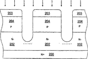
Fig. 2 A illustrates groove MOSFET according to an embodiment of the invention.Shown in groove MOSFET in, epitaxial loayer 201 is set on N+ substrate 200.
N-district 202 is found in bottom at epitaxial loayer 201.In this example, this district for example has 2 to 5 microns thickness range and for example has 4 * 10
15To 8 * 10
16Cm
-3The net dopant concentration scope.
P-tagma 204 is found on top at epitaxial loayer 201.Shown in example in, these P-tagmas 204 have for example 1 to 2 micron thickness range, and for example have 1 * 10
17To 1 * 10
18Cm
-3The net dopant concentration scope.
Be lined with insulator 210 in the groove that forms in epitaxial loayer 201, and fill with conductor 211, insulator 210 all oxides in this way, conductor 211 provide the gate electrode function of device as the polysilicon of doping.Groove generally has about 1.5 to about 2.5 microns degree of depth.Silica (generally being silicon dioxide) is as insulator 210, and it can be the thickness of 500 to 700 dusts for example.Polysilicon is as conductor 211, and it can have for example resistivity of 1 to 15 Ω/sq.Zone between the groove usually is called " table top " or " groove table top " based on their shape.These zones normally square or hexagon in plane graph.
According to the present invention, N district 206 (also referring to " channel bottom injection region " at this) is set between channel bottom and N+ substrate.N district 206 for example has 1 * 10
18To 5 * 10
19Cm
-3The net dopant concentration scope.These zone 206 whole distances of preferably extending from channel bottom to N+ substrate 200, as shown in the figure, if but wish that also partly bridge joint should distance.Generally, these zones have 1 to 6 micron depth bounds.
The groove MOSFET device of Fig. 2 also comprises N+ source region 212, and 0.3 to 0.5 micron the degree of depth is extended from epi-layer surface in N+ source region 212 in illustrated embodiment, and has for example from 5 * 10
19To 5 * 10
20Cm
-3The net dopant concentration scope.
Electrically contact N+ source region 212 by metal source contact 218.Insulation layer as BPSG (boron-phosphorosilicate glass) district 216, prevents that the doped polysilicon area relevant with gate electrode 211 is shorted to N+ source region 212 by source electrode contact 218.The grid that metal gate contact (not shown) separately generally is connected to the polysilicon 211 of the outside, zone that is positioned at the groove MOSFET unit extends (runner) part.Generally also contiguous N+ substrate 200 is provided with metal drain contact (not shown).
Curve shown in Figure 3 is the roughly dopant profile of finding along the line A-A ' part of Fig. 2, and this curve begins and extends to substrate 200 at channel bottom.The left part of curve a is corresponding to N district 206, and the right side part is corresponding to N+ substrate 200.In order to compare, curve b shown in Figure 3 is the roughly dopant profile of finding along the parallel portion of the line B-B ' among Fig. 2.The left part of curve b is corresponding to N-epitaxial region 202, and the right side part is corresponding to N+ substrate 200.
Although do not wish to be bound by theory, think between the multi-crystal silicon area 211 of p-tagma 204 and grid when producing potential difference that charge inducing capacitively in the p-tagma of contiguous gate oxide 210 causes formation raceway groove p-tagma 204 in.When between source region 212 and N+ substrate 200 (corresponding to the drain region), providing another potential difference, electric current flows to N+ substrate 200 from source region 212 by the raceway groove that forms the P-tagma 204 of contiguous gate oxide 210, and groove MOSFET considered to be in the power connection state.Think that further the device of Fig. 2 has the conducting resistance of increase because when transistor is in the energized state, the N district 206 that forms at the matrix place of groove provide the reduction electric current from the source region 212 paths that flow to the impedance in drain region (N+ substrate 200).
Now according to one embodiment of present invention, in conjunction with Fig. 4 A to Fig. 4 C the method that is used to make groove MOSFET shown in Figure 2 is described.
Turn to Fig. 4 A now, the epitaxial loayer 201 that initial growth N mixes on the substrate 200 that N+ mixes.N+ doped substrate 200 is from 10 to 25 mils for example, and for example have 1 * 10
19To 1 * 10
20Cm
-3The net dopant concentration scope.Epitaxial loayer 301 for example can have 4 * 10
15To 8 * 10
16Cm
-3Clean n-type doping content, and the thickness that can have 3 to 10 microns.
The use mask that depends on the circumstances then by injecting and diffusion, forms p type island region 204 in epitaxial loayer 201.For example, epitaxial loayer 201 can inject boron, then at high temperature spreads making p type island region 204, and p type island region 204 can be 1 to 2 micron thickness and for example have 1 * 10
17To 1 * 10
18Cm
-3Clean p-type doping content scope.After this step, the N-part 202 of epitaxial loayer 201 can be left 2 to 5 micron thickness.N-part 202 has the n-type doping content of above-mentioned epitaxial loayer 201.
After the trench mask (not shown) of composition was provided, deposition mask oxide layer 203 for example by chemical vapor deposition, and was passed through reactive ion etching method etching then.The structure of gained has been shown among Fig. 4 A.
Then by the hole in the patterned mask oxide layer 203, generally by reactive ion etching method etching groove.Gash depth in this example is about 1.5 to 2.5 microns.Owing to this groove-formation step is set up discontinuous P-tagma 204.
At this moment, use trench mask n-type dopant (preferred phosphorus) to be injected this structure as injecting mask.In this example, inject 5 * 10 80 to 100keV the time
15To 1 * 10
17Cm
-3The phosphorus of dosage.The structure of gained has been shown among Fig. 4 B.Dotted line below the channel bottom illustrates at structure memory at phosphorus.
According to preferred embodiment,, in the formation sacrificial oxide layer, carry out diffuse dopants although can be spread to structure by the n-type dopant (for example phosphorus) that heating arrangement simply injects this moment.Specifically, carry out 20 to 60 minutes dry oxidations during generally by 900 to 1150 ℃, the sacrificial oxide layer of in groove, growing this moment.As a result, except that forming sacrificial oxide regions 205, the n-type dopant that this elevated temperature step drives is injected forms N district 206 to the N-type district 202 of epitaxial loayer.Illustrate the structure of gained among Fig. 4 C.
Subsequently, finish groove MOSFET, to form the structure shown in Fig. 2.For example, preferably remove the sacrificial oxide regions of seeing Fig. 4 C 205 from groove by wet etching.Carry out 20 to 60 minutes dry oxidations during then for example by 900 to 1100 ℃, the oxide layer of on channel bottom, growing, oxide layer is the thickness of 500 to 700 dusts preferably.The gate oxidation district 210 that these oxide layer parts finally are formed for finishing device.
Use the surface and the filling groove of polysilicon layer covered structure then, preferably use CVD.The polysilicon N-type that generally mixes is to reduce its resistivity.For example can in the CVD process of phosphorus chloride or by injecting, carry out the doping of N-type with arsenic or phosphorus.Then for example by reactive ion etching method etch polysilicon layer.Owing to relate to etching homogeneity, the polysilicon layer in the trench portions is usually by over etching slightly, and therefore the polysilicon gate polar region 211 that forms generally has under the adjacently situated surfaces of epitaxial loayer 204 0.1 to 0.2 micron end face.
The mask layer of composition is set then and via injecting and diffusing procedure forms n+ source region 212 by mask layer on the top of epitaxial loayer, n+ source region 212 is preferably from the degree of depth of 0.3 to 0.5 micron of epi-layer surface extension and have for example from 5 * 10
19To 5 * 10
20Cm
-3The net dopant concentration scope.Preferably inject to avoid injection-channeling effect, injection to damage and heavy metal pollution in the forming process in source region by injecting oxide.
For example on total, form BPSG (boron-phosphorosilicate glass) layer then by PECVD.After setting has the structure of photoresist layer of composition,,, form BPSG district 216 with BPSG on the selected portion of removing structure and oxide layer generally by this structure of reactive ion etching method etching.Remove the photoresist layer of composition then, the depositing metal contact layer forms source electrode contact 218.Grid generally also is set contacts (not shown) with drain electrode.The structure of gained is identical with Fig. 2's.
Although illustrate particularly and described various embodiment, should be appreciated that under the range of condition that does not break away from spirit of the present invention and want improvement of the present invention and change all to be covered, and fall within the scope of the appended claims by above-mentioned training centre at this.As an object lesson, method of the present invention can be used for forming conductivity and those opposite configuration described here of each semiconductor region.
Claims (20)
1. groove MOSFET device comprises:
The substrate of first conduction type;
The epitaxial loayer of described first conduction type on described substrate, described epitaxial loayer have the majority carrier concentration lower than described substrate;
Extend to groove the described epitaxial loayer from the upper surface of described epitaxial loayer;
Liner is to the insulating barrier of the described groove of small part;
Conduction region in the described groove of contiguous described insulating barrier;
The doped region of described first conduction type that forms in the described epitaxial loayer between described channel bottom and described substrate, described doped region has the majority carrier concentration that is lower than described substrate and is higher than described epitaxial loayer, described doped region extends at described channel bottom, and wideer than described channel bottom, the distance that described doped region extends be from described channel bottom to described substrate distance 100%;
In the top of described epitaxial loayer and the tagma of second conduction type that forms of contiguous described groove, the degree of depth that the degree of depth that extend from the described upper surface of described epitaxial loayer in described tagma is extended less than described groove; With
In the top in described tagma and the source region of described first conduction type that forms of contiguous described groove.
2. groove MOSFET device as claimed in claim 1, wherein, described first conduction type is a n-type conduction, the described second conduction type p-type conductivity.
3. groove MOSFET device as claimed in claim 2, wherein, described doped region phosphorus doping.
4. groove MOSFET device as claimed in claim 2, wherein, described substrate is the N+ substrate, and described epitaxial loayer is the N-epitaxial loayer, and described doped region is the N district, and described tagma is the P district, and described source region is the N+ district.
5. groove MOSFET device as claimed in claim 1, wherein, described groove MOSFET device is a silicon device.
6. groove MOSFET device as claimed in claim 1, wherein, described insulating barrier is a silicon oxide layer.
7. groove MOSFET device as claimed in claim 5, wherein, described conduction region is the multi-crystal silicon area that mixes.
8. groove MOSFET device as claimed in claim 1, wherein, from 1 to 6 micron of the thickness range of the doped region between channel bottom and the substrate.
9. groove MOSFET device as claimed in claim 2, wherein, described doped region has 1 * 10
18To 5 * 10
19Cm
-3Clean n-type carrier concentration scope.
10. groove MOSFET device as claimed in claim 1, wherein, described groove limits one of square and hexagonal MOSFET unit.
11. a groove MOSFET device comprises:
The silicon substrate of n-type conduction;
The silicon epitaxy layer of the n-type conduction on described substrate, described epitaxial loayer has the majority carrier concentration lower than described substrate;
Extend to groove the described epitaxial loayer from the upper surface of described epitaxial loayer;
Liner is to the insulating layer of silicon oxide of the described groove of small part;
Doped polysilicon area in the described groove of contiguous described silicon oxide layer;
The doped region of the n-type conduction that between the bottom of described groove and described substrate, is provided with, described doped region has the majority carrier concentration that is lower than described substrate and is higher than described epitaxial loayer, described doped region extends at described channel bottom, and wideer than described channel bottom, the distance that described doped region extends be from described channel bottom to described substrate distance 100%;
In the top of described epitaxial loayer and the tagma of the p-type conduction that forms of contiguous described groove, the degree of depth that the degree of depth that extend from the described upper surface of described epitaxial loayer in described tagma is extended less than described groove; With
In the top in described tagma and the source region of the n-type conduction that forms of contiguous described groove.
12. groove MOSFET device as claimed in claim 11, wherein, described doped region phosphorus doping.
13. groove MOSFET device as claimed in claim 11, wherein, from 1 to 6 micron of the thickness range of the doped region between channel bottom and the substrate.
14. groove MOSFET device as claimed in claim 11, wherein, described doped region has 1 * 10
18To 5 * 10
19Cm
-3Clean n-type carrier concentration scope.
15. a method that forms groove MOSFET device comprises:
The substrate of first conduction type is set;
The epitaxial loayer of described first conduction type of deposit on described substrate, described epitaxial loayer have the majority carrier concentration lower than described substrate;
In the top of described epitaxial loayer, form the tagma of second conduction type;
Etching extends to the groove of described epitaxial loayer from the upper surface of described epitaxial loayer, the degree of depth that described groove has sidepiece and bottom and extends greater than described tagma from the degree of depth that the described upper surface of described epitaxial loayer extends;
Form the doped region of described first conduction type between described channel bottom and described substrate, described doped region has the majority carrier concentration that is lower than described substrate and is higher than described epitaxial loayer;
Wherein, described doped region spread and extend to from described channel bottom to described substrate distance 100%, and
Wherein, the step of described groove of described etching and the described doped region of formation comprises: (a) directly form trench mask on described epitaxial loayer; (b) by the described groove of described trench mask etching; (c) inject the dopant of described first conduction type by described trench mask; And the described dopant that (d) spreads described first conduction type in the temperature that raises;
Form the insulating barrier of liner to the described groove of small part;
In the described groove of contiguous described insulating barrier, form conduction region; With
At the described groove of described etching with after forming the step of described doped region, in the top in described tagma and contiguous described groove form the source region of described first conduction type.
16. method as claimed in claim 15, wherein, described first conduction type is a n-type conduction, described second conduction type p-type conduction.
17. method as claimed in claim 16, wherein, described dopant is a phosphorus.
18. method as claimed in claim 15, wherein, described groove MOSFET device is a silicon device.
19. method as claimed in claim 15 also comprises:
Contiguous described Semiconductor substrate forms the metal-drain contact,
The upper surface in contiguous described source region form the metal source contact and
Vicinity forms the metal gates contact away from the upper surface of the described conduction region in described source region.
20. a method that forms groove MOSFET device comprises:
The substrate of first conduction type is set;
The epitaxial loayer of described first conduction type of deposit on described substrate, described epitaxial loayer have the majority carrier concentration lower than described substrate;
In the top of described epitaxial loayer, form the tagma of second conduction type;
Etching extends to the groove with sidepiece and bottom of described epitaxial loayer from the upper surface of described epitaxial loayer, the degree of depth that described groove extends greater than described tagma from the degree of depth that the described upper surface of described epitaxial loayer extends;
Form the doped region of described first conduction type between described channel bottom and described substrate, described doped region has the majority carrier concentration that is lower than described substrate and is higher than described epitaxial loayer;
Wherein, the step of described groove of described etching and the described doped region of formation comprises: (a) form trench mask on described epitaxial loayer; (b) by the described groove of described trench mask etching; (c) inject the dopant of described first conduction type by described trench mask; And the described dopant that (d) spreads described first conduction type in the temperature that raises;
Form the insulating barrier of liner to the described groove of small part;
In the described groove of contiguous described insulating barrier, form conduction region; With
At the described groove of described etching with after forming the step of described doped region, in the top in described tagma and contiguous described groove form the source region of described first conduction type,
The temperature of described rising wherein, is provided by the step along described trench wall growth sacrifical oxide.
Applications Claiming Priority (2)
| Application Number | Priority Date | Filing Date | Title |
|---|---|---|---|
| US09/999,116 | 2001-11-21 | ||
| US09/999,116 US6657254B2 (en) | 2001-11-21 | 2001-11-21 | Trench MOSFET device with improved on-resistance |
Publications (2)
| Publication Number | Publication Date |
|---|---|
| CN1695252A CN1695252A (en) | 2005-11-09 |
| CN100474616C true CN100474616C (en) | 2009-04-01 |
Family
ID=25545922
Family Applications (1)
| Application Number | Title | Priority Date | Filing Date |
|---|---|---|---|
| CNB028232461A Expired - Fee Related CN100474616C (en) | 2001-11-21 | 2002-11-20 | Trench MOSFET device with improved on-resistance |
Country Status (8)
| Country | Link |
|---|---|
| US (2) | US6657254B2 (en) |
| EP (1) | EP1454360A4 (en) |
| JP (1) | JP2005510881A (en) |
| KR (1) | KR100957584B1 (en) |
| CN (1) | CN100474616C (en) |
| AU (1) | AU2002348308A1 (en) |
| TW (1) | TW200300593A (en) |
| WO (1) | WO2003046997A1 (en) |
Cited By (1)
| Publication number | Priority date | Publication date | Assignee | Title |
|---|---|---|---|---|
| CN102064194A (en) * | 2009-11-12 | 2011-05-18 | 三星电子株式会社 | Recessed channel transistor devices, display apparatuses including recessed channel transistor devices, and methods of fabricating recessed channel transistor devices |
Families Citing this family (53)
| Publication number | Priority date | Publication date | Assignee | Title |
|---|---|---|---|---|
| US20060038223A1 (en) * | 2001-07-03 | 2006-02-23 | Siliconix Incorporated | Trench MOSFET having drain-drift region comprising stack of implanted regions |
| US7033876B2 (en) * | 2001-07-03 | 2006-04-25 | Siliconix Incorporated | Trench MIS device having implanted drain-drift region and thick bottom oxide and process for manufacturing the same |
| US7009247B2 (en) * | 2001-07-03 | 2006-03-07 | Siliconix Incorporated | Trench MIS device with thick oxide layer in bottom of gate contact trench |
| US7291884B2 (en) * | 2001-07-03 | 2007-11-06 | Siliconix Incorporated | Trench MIS device having implanted drain-drift region and thick bottom oxide |
| US6784505B2 (en) * | 2002-05-03 | 2004-08-31 | Fairchild Semiconductor Corporation | Low voltage high density trench-gated power device with uniformly doped channel and its edge termination technique |
| US6919599B2 (en) * | 2002-06-28 | 2005-07-19 | International Rectifier Corporation | Short channel trench MOSFET with reduced gate charge |
| US7576388B1 (en) | 2002-10-03 | 2009-08-18 | Fairchild Semiconductor Corporation | Trench-gate LDMOS structures |
| US7638841B2 (en) | 2003-05-20 | 2009-12-29 | Fairchild Semiconductor Corporation | Power semiconductor devices and methods of manufacture |
| JP3954541B2 (en) * | 2003-08-05 | 2007-08-08 | 株式会社東芝 | Semiconductor device and manufacturing method thereof |
| KR100541139B1 (en) * | 2003-10-02 | 2006-01-11 | 주식회사 케이이씨 | Trench MOS and its manufacturing method |
| US7368777B2 (en) | 2003-12-30 | 2008-05-06 | Fairchild Semiconductor Corporation | Accumulation device with charge balance structure and method of forming the same |
| US7045857B2 (en) * | 2004-03-26 | 2006-05-16 | Siliconix Incorporated | Termination for trench MIS device having implanted drain-drift region |
| US7352036B2 (en) | 2004-08-03 | 2008-04-01 | Fairchild Semiconductor Corporation | Semiconductor power device having a top-side drain using a sinker trench |
| US7262111B1 (en) * | 2004-09-07 | 2007-08-28 | National Semiconductor Corporation | Method for providing a deep connection to a substrate or buried layer in a semiconductor device |
| KR100582374B1 (en) * | 2004-09-08 | 2006-05-22 | 매그나칩 반도체 유한회사 | High voltage transistor and method for fabricating the same |
| JP2006156461A (en) * | 2004-11-25 | 2006-06-15 | Shindengen Electric Mfg Co Ltd | Semiconductor device and its manufacturing method |
| WO2006108011A2 (en) * | 2005-04-06 | 2006-10-12 | Fairchild Semiconductor Corporation | Trenched-gate field effect transistors and methods of forming the same |
| JP2008546189A (en) * | 2005-05-26 | 2008-12-18 | フェアチャイルド・セミコンダクター・コーポレーション | Trench gate field effect transistor and method of manufacturing the same |
| AT504290A2 (en) | 2005-06-10 | 2008-04-15 | Fairchild Semiconductor | FIELD EFFECT TRANSISTOR WITH LOAD BALANCE |
| JP2007173675A (en) * | 2005-12-26 | 2007-07-05 | Toyota Central Res & Dev Lab Inc | Semiconductor device and its manufacturing method |
| CN101443889B (en) * | 2006-05-12 | 2012-08-29 | 维西埃-硅化物公司 | Power metal semiconductor field effect transistor contact metallization |
| US7319256B1 (en) | 2006-06-19 | 2008-01-15 | Fairchild Semiconductor Corporation | Shielded gate trench FET with the shield and gate electrodes being connected together |
| US7750398B2 (en) * | 2006-09-26 | 2010-07-06 | Force-Mos Technology Corporation | Trench MOSFET with trench termination and manufacture thereof |
| JP4294050B2 (en) * | 2006-12-27 | 2009-07-08 | 三洋電機株式会社 | Semiconductor device and manufacturing method thereof |
| DE102007014038B4 (en) | 2007-03-23 | 2015-02-12 | Infineon Technologies Austria Ag | Method for producing a semiconductor component |
| US7615847B2 (en) * | 2007-03-23 | 2009-11-10 | Infineon Technologies Austria Ag | Method for producing a semiconductor component |
| DE102007029121B3 (en) | 2007-06-25 | 2008-11-20 | Infineon Technologies Austria Ag | Method for producing a semiconductor component, and semiconductor component |
| EP2208229A4 (en) | 2007-09-21 | 2011-03-16 | Fairchild Semiconductor | Superjunction structures for power devices and methods of manufacture |
| US7772668B2 (en) | 2007-12-26 | 2010-08-10 | Fairchild Semiconductor Corporation | Shielded gate trench FET with multiple channels |
| KR100988776B1 (en) * | 2007-12-27 | 2010-10-20 | 주식회사 동부하이텍 | Method of manufacturing a recessed gate transistor |
| JP2010219109A (en) * | 2009-03-13 | 2010-09-30 | Sanken Electric Co Ltd | Trench gate type semiconductor device, and method of manufacturing the same |
| DE102009021485B4 (en) * | 2009-05-15 | 2017-10-05 | Globalfoundries Dresden Module One Llc & Co. Kg | Semiconductor device having a metal gate and a silicon-containing resistor formed on an insulating structure and method for its production |
| CN101997030B (en) * | 2009-08-17 | 2012-07-04 | 力士科技股份有限公司 | Trench metal-oxide-semiconductor field effect transistor (MOSFET) with shallow trench structure and manufacturing method thereof |
| CN101673673B (en) * | 2009-09-22 | 2013-02-27 | 上海宏力半导体制造有限公司 | Method for forming epitaxial wafer and epitaxial wafer formed by using same |
| KR101751908B1 (en) * | 2009-10-21 | 2017-06-28 | 가부시키가이샤 한도오따이 에네루기 켄큐쇼 | Voltage regulator circuit |
| CN102244095B (en) * | 2010-05-11 | 2013-05-22 | 力士科技股份有限公司 | Power semiconductor device |
| US8432000B2 (en) | 2010-06-18 | 2013-04-30 | Fairchild Semiconductor Corporation | Trench MOS barrier schottky rectifier with a planar surface using CMP techniques |
| TWI453827B (en) * | 2010-08-20 | 2014-09-21 | Csmc Technologies Fab1 Co Ltd | Vertical NPN transistor and its manufacturing method |
| US20120126341A1 (en) * | 2010-11-23 | 2012-05-24 | Microchip Technology Incorporated | Using low pressure epi to enable low rdson fet |
| US8823090B2 (en) | 2011-02-17 | 2014-09-02 | International Business Machines Corporation | Field-effect transistor and method of creating same |
| JP5729331B2 (en) * | 2011-04-12 | 2015-06-03 | 株式会社デンソー | Semiconductor device manufacturing method and semiconductor device |
| US8492903B2 (en) | 2011-06-29 | 2013-07-23 | International Business Machines Corporation | Through silicon via direct FET signal gating |
| KR101108697B1 (en) * | 2011-09-29 | 2012-01-25 | 주식회사 코아스 | Mounting device and bed therewith |
| CN102945843B (en) * | 2012-11-30 | 2016-12-21 | 上海华虹宏力半导体制造有限公司 | Detection structure and resistance measurement method |
| US9006063B2 (en) * | 2013-06-28 | 2015-04-14 | Stmicroelectronics S.R.L. | Trench MOSFET |
| US9136368B2 (en) * | 2013-10-03 | 2015-09-15 | Texas Instruments Incorporated | Trench gate trench field plate semi-vertical semi-lateral MOSFET |
| JP5976137B2 (en) * | 2015-01-14 | 2016-08-23 | ソフトバンク株式会社 | Mobile station speed estimation method using Doppler spectrum in mobile communication system |
| US11018253B2 (en) * | 2016-01-07 | 2021-05-25 | Lawrence Livermore National Security, Llc | Three dimensional vertically structured electronic devices |
| CN107342226B (en) * | 2017-07-19 | 2020-07-31 | 无锡新洁能股份有限公司 | Manufacturing method of ultra-small unit size longitudinal super junction semiconductor device |
| DE102017124872B4 (en) * | 2017-10-24 | 2021-02-18 | Infineon Technologies Ag | Method for manufacturing an IGBT with dV / dt controllability |
| CN113745339B (en) * | 2021-09-07 | 2022-08-19 | 无锡新洁能股份有限公司 | High-reliability power semiconductor device and manufacturing method thereof |
| CN114597130B (en) * | 2022-04-02 | 2022-12-27 | 致瞻科技(上海)有限公司 | Silicon carbide MOSFET device based on split gate and manufacturing method thereof |
| CN114613848B (en) * | 2022-05-10 | 2022-07-19 | 南京微盟电子有限公司 | Low-voltage trench gate power device and manufacturing method thereof |
Family Cites Families (15)
| Publication number | Priority date | Publication date | Assignee | Title |
|---|---|---|---|---|
| US4893160A (en) | 1987-11-13 | 1990-01-09 | Siliconix Incorporated | Method for increasing the performance of trenched devices and the resulting structure |
| US5072266A (en) | 1988-12-27 | 1991-12-10 | Siliconix Incorporated | Trench DMOS power transistor with field-shaping body profile and three-dimensional geometry |
| JP2635828B2 (en) * | 1991-01-09 | 1997-07-30 | 株式会社東芝 | Semiconductor device |
| JPH0621468A (en) * | 1992-06-29 | 1994-01-28 | Toshiba Corp | Insulated gate semiconductor device |
| US5410170A (en) | 1993-04-14 | 1995-04-25 | Siliconix Incorporated | DMOS power transistors with reduced number of contacts using integrated body-source connections |
| JP3400846B2 (en) | 1994-01-20 | 2003-04-28 | 三菱電機株式会社 | Semiconductor device having trench structure and method of manufacturing the same |
| US5424231A (en) * | 1994-08-09 | 1995-06-13 | United Microelectronics Corp. | Method for manufacturing a VDMOS transistor |
| US6084268A (en) * | 1996-03-05 | 2000-07-04 | Semiconductor Components Industries, Llc | Power MOSFET device having low on-resistance and method |
| EP2043158B1 (en) * | 1996-07-19 | 2013-05-15 | SILICONIX Incorporated | Trench DMOS transistor with trench bottom implant |
| JP3915180B2 (en) * | 1997-07-03 | 2007-05-16 | 富士電機デバイステクノロジー株式会社 | Trench type MOS semiconductor device and manufacturing method thereof |
| US6262453B1 (en) * | 1998-04-24 | 2001-07-17 | Magepower Semiconductor Corp. | Double gate-oxide for reducing gate-drain capacitance in trenched DMOS with high-dopant concentration buried-region under trenched gate |
| JP2000269487A (en) * | 1999-03-15 | 2000-09-29 | Toshiba Corp | Semiconductor device and its manufacture |
| JP2001036071A (en) * | 1999-07-16 | 2001-02-09 | Toshiba Corp | Manufacture for semiconductor device |
| JP2001102576A (en) * | 1999-09-29 | 2001-04-13 | Sanyo Electric Co Ltd | Semiconductor device |
| US6285060B1 (en) * | 1999-12-30 | 2001-09-04 | Siliconix Incorporated | Barrier accumulation-mode MOSFET |
-
2001
- 2001-11-21 US US09/999,116 patent/US6657254B2/en not_active Expired - Lifetime
-
2002
- 2002-11-19 TW TW091133747A patent/TW200300593A/en unknown
- 2002-11-20 KR KR1020047007618A patent/KR100957584B1/en not_active IP Right Cessation
- 2002-11-20 EP EP02782334A patent/EP1454360A4/en not_active Ceased
- 2002-11-20 CN CNB028232461A patent/CN100474616C/en not_active Expired - Fee Related
- 2002-11-20 JP JP2003548314A patent/JP2005510881A/en active Pending
- 2002-11-20 AU AU2002348308A patent/AU2002348308A1/en not_active Abandoned
- 2002-11-20 WO PCT/US2002/037265 patent/WO2003046997A1/en active Application Filing
-
2003
- 2003-12-01 US US10/725,325 patent/US7094640B2/en not_active Expired - Lifetime
Cited By (1)
| Publication number | Priority date | Publication date | Assignee | Title |
|---|---|---|---|---|
| CN102064194A (en) * | 2009-11-12 | 2011-05-18 | 三星电子株式会社 | Recessed channel transistor devices, display apparatuses including recessed channel transistor devices, and methods of fabricating recessed channel transistor devices |
Also Published As
| Publication number | Publication date |
|---|---|
| TW200300593A (en) | 2003-06-01 |
| KR20040053339A (en) | 2004-06-23 |
| US6657254B2 (en) | 2003-12-02 |
| JP2005510881A (en) | 2005-04-21 |
| CN1695252A (en) | 2005-11-09 |
| WO2003046997A1 (en) | 2003-06-05 |
| EP1454360A4 (en) | 2008-12-17 |
| US20030094624A1 (en) | 2003-05-22 |
| US7094640B2 (en) | 2006-08-22 |
| US20040113203A1 (en) | 2004-06-17 |
| AU2002348308A1 (en) | 2003-06-10 |
| EP1454360A1 (en) | 2004-09-08 |
| KR100957584B1 (en) | 2010-05-13 |
Similar Documents
| Publication | Publication Date | Title |
|---|---|---|
| CN100474616C (en) | Trench MOSFET device with improved on-resistance | |
| KR100305978B1 (en) | Field-effect trench transistors with lightly doped epitaxial regions on the surface of transistors | |
| CN100375293C (en) | Trench MOSFET device with polycrystalline silicon source contact structure | |
| CN100477255C (en) | Trench MOSFET with structure having low gate charge | |
| KR100270796B1 (en) | Process for manufacture of mos gated device with selef aligned cells | |
| US6586800B2 (en) | Trench-gate semiconductor devices | |
| CN103650148B (en) | Igbt | |
| JP4429601B2 (en) | MOS gate power device having segmented trench and extended doping zone, and manufacturing method thereof | |
| US6177704B1 (en) | Semiconductor device containing a lateral MOS transistor | |
| KR100451450B1 (en) | Field effect transistor arrangement with a trench gate electrode and an additional highly doped layer in the body region | |
| KR100990294B1 (en) | High voltage power mosfet includes doped columns | |
| CN105977290A (en) | Semiconductor device, integrated circuit and method of manufacturing semiconductor device | |
| CN101889327A (en) | Method for fabricating a power semiconductor device having a voltage sustaining layer with a terraced trench facilitating formation of floating islands | |
| CN104752492B (en) | The method and semiconductor devices being used for producing the semiconductor devices | |
| CN1539169A (en) | Symmetric trench MOSFET device and method of making same | |
| CN106571394A (en) | Power device and manufacturing method thereof | |
| CN100463122C (en) | High voltage power MOSFET having low on-resistance | |
| KR100948663B1 (en) | Method of forming device comprising a plurality of trench mosfet cells, and method of forming shallow and deep dopant implants | |
| CN101989602B (en) | Trench MOSFET | |
| CN101026192A (en) | Semiconductor device and method of manufacturing the same | |
| CN101989577B (en) | Method for manufacturing groove MOSFET (Metal-Oxide -Semiconductor Field Effect Transistor) | |
| CN113659011A (en) | Integrated device based on super junction MOSFET and manufacturing method thereof | |
| CN102810565A (en) | Semiconductor power device | |
| CN103094342B (en) | Power transistor device and manufacturing method thereof | |
| KR100492981B1 (en) | Lateral double diffusion MOS transistor and manufacturing method thereof |
Legal Events
| Date | Code | Title | Description |
|---|---|---|---|
| C06 | Publication | ||
| PB01 | Publication | ||
| C10 | Entry into substantive examination | ||
| SE01 | Entry into force of request for substantive examination | ||
| C14 | Grant of patent or utility model | ||
| GR01 | Patent grant | ||
| CF01 | Termination of patent right due to non-payment of annual fee |
Granted publication date: 20090401 Termination date: 20171120 |
|
| CF01 | Termination of patent right due to non-payment of annual fee |