Summary of the invention
The present invention proposes in view of the foregoing, its purpose is, a kind of influence that is not subject to drive transistor characteristics difference is provided, can be driven device to current modes such as similar organic EL devices, supply with element circuit, electronic circuit, electro-optical device, driving method and the e-machine of target current.
In order to reach described purpose, the invention is characterized in, comprising: be driven device; Control flows to the described driving transistors that is driven the magnitude of current of device; The capacity cell that is connected with the grid of described driving transistors; And directly be connected with described grid and constitute the compensation transistor that diode connects, corresponding by described compensation transistor, as the data current that data-signal is supplied with, set the conducting state of described driving transistors.According to this formation, for example, because compensation transistor directly is connected with the grid of driving transistors, institute is so that these two transistors result of approaching setting mutually can become easy to these two characteristics of transistor being reached unanimity and adjusting the characteristic ratio.In addition, flow through the data current of compensation transistor, be directly reflected on the magnitude of current of controlling by driving transistors.At this, it is constituted: comprise described compensation transistor and the 1st switching transistor that is connected in series by a utmost point in source electrode or the drain electrode, another utmost point in the source electrode of described the 1st switching transistor or the drain electrode, be connected with signal wire, and when by described the 1st switching transistor described signal wire being electrically connected with described compensation transistor, described data current flows through described compensation transistor.
In addition, in order to reach described purpose, the present invention is to comprise: be driven device; Control flows to the described driving transistors that is driven the magnitude of current of device; The capacity cell that is connected with the grid of described driving transistors; The 1st switching transistor that is connected with the grid of described driving transistors; The 1st signal wire that is connected with the grid of described the 1st switching transistor; The 2nd signal wire that is connected with the source electrode or a utmost point in the drain electrode of described the 1st switching transistor; And the element circuit that applies the power lead of supply voltage, it is characterized in that, between the source electrode or another utmost point in the drain electrode of described power lead and described the 1st switching transistor, have the compensation transistor and the 2nd switching transistor that are connected in series, described compensation transistor constitutes diode and connects, and the grid of described the 2nd switching transistor is connected with the 3rd signal wire that is different from described the 1st signal wire.In addition, the present invention is to comprise: the device that is driven that is subjected to current drives; Control flows to the described driving transistors that is driven the magnitude of current of device; The capacity cell that is connected with the grid of described driving transistors; The 1st switching transistor that is connected with the grid of described driving transistors; The 1st signal wire that is connected with the grid of described the 1st switching transistor; The 2nd signal wire that is connected with the source electrode or a utmost point in the drain electrode of described the 1st switching transistor; And the element circuit that applies the power lead of supply voltage, it is characterized in that, between the source electrode or another utmost point in the drain electrode of described power lead and described the 1st switching transistor, compensation transistor and the 2nd switching transistor have been connected in series, described compensation transistor constitutes diode and connects, and the grid of described the 2nd switching transistor is connected with described the 1st signal wire.No matter which kind of constitutes, heterogeneity that all can compensation for drive transistor.At this, if last formation and back one are constituted when comparing, in back one constitutes, because the grid of the 1st and the 2nd switching transistor is connected with same signal wire, thus do not need the 3rd signal wire, thereby can reduce wiring quantity.In addition, the so-called transistor that constitutes the diode connection is exactly a utmost point in its source electrode or the drain electrode, is in the transistor of the state that is connected with grid.In addition, in last formation, preferably make its constitute be provided with make described the 1st switching transistor and described the 2nd switching transistor all become conducting state during.
At this, in last formation and back one formation, preferably constitute and make described the 2nd signal wire, be the data line of supplying with as the electric current of data-signal.
In addition, also can constitute and make correspondence flow through the electric charge of the magnitude of current of described compensation transistor, be accumulated in the described capacity cell.
Though in described driving transistors and described compensation transistor, also wish roughly the same with respect to the current characteristics between the source electrode-drain electrode of grid voltage, make the magnitude of current that flows through described compensation transistor but also can constitute, greater than the magnitude of current of controlling by described driving transistors.
Have, preferably making the described device that is driven is organic electroluminescenoe device again.
In addition, preferably make described driving transistors, the described the 1st and the 2nd switching transistor and described compensation transistor, be respectively thin film transistor (TFT), and for described driving transistors, preferably with changing little P channel-type between the operating period.
In order to reach described purpose, the invention is characterized in, comprising: corresponding supply to sweep signal on the 1st sweep trace and conducting or by and source electrode or drain electrode in the 1st switching transistor that is connected with data line of a utmost point; Play the compensation transistor of diode action in compensation transistor that is connected in series between another utmost point in the source electrode of power lead that applies supply voltage and described the 1st switching transistor or drain electrode and the 2nd switching transistor; Correspondingly supply to sweep signal on the 2nd sweep trace different and conducting or the 2nd switching transistor that ends with described the 1st sweep trace; Grid is connected, drives the driving transistors that is driven device with the source electrode of described the 1st switching transistor or another utmost point in the drain electrode; And the capacity cell that keeps the grid voltage of described driving transistors.
In addition, the invention is characterized in, comprising: corresponding supply to sweep signal on the 1st sweep trace and conducting or by and source electrode or drain electrode in the 1st switching transistor that is connected with data line of a utmost point; Play the compensation transistor of diode action in compensation transistor that is connected in series between another utmost point in the source electrode of power lead that applies supply voltage and described the 1st switching transistor or drain electrode and the 2nd switching transistor; Correspondingly supply to sweep signal on described the 1st sweep trace and conducting or the 2nd switching transistor that ends; Grid is connected, drives the driving transistors that is driven device with the source electrode of described the 1st switching transistor or another utmost point in the drain electrode; And the capacity cell that keeps the grid voltage of described driving transistors.No matter which kind of constitutes, heterogeneity that all can compensation for drive transistor.At this, if last formation and back one are constituted when comparing, in back one constitutes, because the grid of the 1st and the 2nd switching transistor is connected with same signal wire, thus do not need the 2nd signal wire, thereby can reduce wiring quantity.
In order to reach described purpose, the invention is characterized in, comprising: correspondingly supply to sweep signal on the sweep trace and a conducting or a switching transistor that the utmost point is connected with data line in, source electrode or drain electrode; At least a portion in the conduction period of described switching transistor or apply the 1st power lead of the 1st supply voltage in the whole period and the source electrode of described switching transistor or drain electrode in another utmost point between play the compensation transistor of diode action; Grid is connected with source electrode or another utmost point in the drain electrode of described switching transistor, self the source electrode or a utmost point in the drain electrode are connected, also drive the driving transistors that is driven device with the 2nd power lead that applies the 2nd supply voltage; And the capacity cell that keeps the grid voltage of described driving transistors.
In addition, the invention is characterized in, comprising: grid is connected with the sweep trace of supplying with sweep signal, a switching transistor that the utmost point is connected with data line in source electrode or the drain electrode; In the compensation transistor that grid and source electrode or drain electrode are connected, a utmost point in source electrode or the drain electrode, with corresponding described sweep signal in the conduction period of described switching transistor at least a portion or in the whole period, the 1st power lead that applies the 1st supply voltage is connected, another utmost point in source electrode of self or the drain electrode, the compensation transistor that is connected with source electrode or another utmost point in the drain electrode of described switching transistor; When another utmost point in the source electrode of grid and described switching transistor or the drain electrode is connected, the source electrode of self or the driving transistors that a utmost point in the drain electrode is connected with the 2nd power lead that applies the 2nd supply voltage, also driving is driven device; And the capacity cell that keeps the grid voltage of described driving transistors.No matter which kind of constitutes, heterogeneity that all can compensation for drive transistor, and can reduce by a transistor.
At this, preferably make described the 1st supply voltage and described the 2nd supply voltage about equally.
In addition, also can be at least with a described element circuit, constitute electro-optical device, memory storage, and various electronic installations such as sensing device.For example, if described element circuit can be constituted electro-optical device as image element circuit.Also this electro-optical device can be installed on e-machine.
In order to reach described purpose, the invention is characterized in to have a plurality of element circuits, each circuit in described a plurality of element circuits comprises: the driving transistors with the 1st terminal and the 2nd terminal; Has the compensation transistor that the 3rd terminal and the 4th terminal, described the 3rd terminal are connected with the grid of described driving transistors; Has the switching transistor that the 5th terminal and the 6th terminal, described the 5th terminal are connected with the grid and described the 3rd terminal of described driving transistors; The quantity of electric charge that keeps the electric current of corresponding flow through described compensation transistor and described switching transistor, and the capacity cell that the one end is connected with the grid of described driving transistors, described the 4th terminal, described the 4th terminal of other element circuit in described a plurality of element circuits, be connected with the 1st power lead, described the 2nd terminal is connected with the 2nd power lead, and have with described the 1st power lead be set in multiple current potential and, control described the 1st power lead and power supply potential and disconnect and the control circuit of connecting.According to this formation, can be by the simple threshold voltage that constitutes compensation for drive transistor.
In each circuit of described element circuit in this electronic circuit, there is not the transistor except described driving transistors, described compensation transistor and described switching transistor.Therefore, threshold voltage that not only can compensation for drive transistor is compared with existing circuit and can also be reduced by an employed transistorized number.
In this electronic circuit, the grid of described compensation transistor is connected with described the 3rd terminal.Therefore, can be by charging into the voltage of capacity cell, the electric current of driving transistors is flow through in control.
In this electronic circuit, described driving transistors is identical with the conduction type of described compensation transistor.Thereby, can compensate driving transistors easily.
In this electronic circuit, on described the 1st terminal, be connected with electron device.Because the threshold voltage of driving transistors is compensated, so can control the current value that flows through electron device accurately.In addition, electron device is the device that is driven that is subjected to current drives.
In this electronic circuit, described control circuit is the transistor that comprises the 7th terminal and the 8th terminal, and described the 7th terminal is connected with power supply, and described the 8th terminal is connected with described the 1st power lead.Like this, can constitute control circuit easily.
In this electronic circuit, electric current flow through described compensation transistor and described switching transistor during, make the current potential of described the 1st power lead and described the 2nd power lead be essentially idiostatic at least.Like this, that can generate by compensation transistor and the approximately equalised voltage of threshold voltage driving transistors supply on the grid of this driving transistors reliably.
In this electronic circuit, described the 1st power lead and described the 2nd power lead can be electrically connected with the power supply with same potential.Like this, can make the voltage approximately equal that supplies on the 1st power lead and the 2nd power lead easily.
In this electronic circuit, with the threshold voltage settings of described driving transistors for not being higher than the threshold voltage of described compensation transistor.Like this, can be reliably the threshold voltage of driving transistors be compensated.
In this electronic circuit, preferably make the magnitude of current that flows through described compensation transistor, greater than the magnitude of current of controlling by described driving transistors.According to this formation, when the switching transistor conducting, the electric charge that correspondence flows through the magnitude of current of this switching transistor and compensation transistor is accumulated in the capacity cell rapidly.
Also can be at least with a described electronic circuit, configuration example such as electro-optical device, memory storage, and various electronic installations such as sensing device.
In addition, the invention is characterized in to have a plurality of element circuits, each circuit in described a plurality of element circuits comprises: the driving transistors with the 1st terminal and the 2nd terminal; Has the compensation transistor that the 3rd terminal and the 4th terminal, described the 3rd terminal are connected with the grid of described driving transistors; Has the switching transistor that the 5th terminal and the 6th terminal, described the 5th terminal are connected with the grid and described the 3rd terminal of described driving transistors; The electrooptics device that is connected with described the 1st terminal; The quantity of electric charge that keeps the electric current of corresponding flow through described compensation transistor and described switching transistor, and the capacity cell that the one end is connected with the grid of described driving transistors, the 1st power lead that is connected with described the 4th terminal, also with described a plurality of element circuits in described the 4th terminal of at least one other element circuit be connected jointly, described the 2nd terminal is connected with the 2nd power lead, and have with described the 1st power lead be set in multiple current potential and, control described the 1st power lead and power supply potential and disconnect and the control circuit of connecting.Like this, threshold voltage that not only can compensation for drive transistor is compared with existing circuit and can be reduced by an employed transistor, thereby, can improve aperture opening ratio, improve display quality.In addition, owing to compare the transistorized number that can reduce by a formation element circuit with existing circuit, so can improve yield rate.
In this electro-optical device, described electrooptics device is an organic EL device.Like this, compare by reducing by an employed transistor, can improve aperture opening ratio with existing circuit, and, the brightness degree during organic EL can be controlled accurately.
In this electro-optical device, described control circuit is the transistor that comprises the 7th terminal and the 8th terminal, and described the 7th terminal is connected with power supply, and described the 8th terminal is connected with described the 1st power lead.Like this, threshold voltage that not only can compensation for drive transistor is compared to constitute easily with existing circuit and is reduced by an employed transistorized element circuit.
In this electro-optical device, electric current flow through described compensation transistor and described switching transistor during, make the current potential of described the 1st power lead and described the 2nd power lead be essentially idiostatic at least.Like this, can will supply to reliably on the grid of this driving transistors with the approximately equalised voltage of threshold voltage driving transistors by that compensation transistor generates.
In this electro-optical device, described the 1st power lead and described the 2nd power lead can be electrically connected with the power supply with same potential.Like this, can make the voltage approximately equal that supplies on the 1st power lead and the 2nd power lead easily.
In this electro-optical device, with the threshold voltage settings of described driving transistors for not being higher than the threshold voltage of described compensation transistor.Like this, can be reliably the threshold voltage of driving transistors be compensated.Therefore, can control the brightness degree of electrooptics device accurately.
The present invention is a kind of electro-optical device, comprising: the multi-strip scanning line; Many data lines; The element circuit that each cross part of corresponding described multi-strip scanning line and described many data lines is provided with respectively; And many articles the 1st power leads, it is characterized in that each circuit in the described element circuit comprises: driving transistors with the 1st terminal and the 2nd terminal; Has the compensation transistor that the 3rd terminal and the 4th terminal, described the 3rd terminal are connected with the grid of described driving transistors; Has the switching transistor that the 5th terminal and the 6th terminal, described the 5th terminal are connected with the grid and described the 3rd terminal of described driving transistors; The electrooptics device that is connected with described the 1st terminal; The quantity of electric charge that keeps the electric current of corresponding flow through described compensation transistor and described switching transistor, and the capacity cell that the one end is connected with the grid of described driving transistors, the grid of the switching transistor in a succession of element circuit is connected jointly with a sweep trace, the 4th terminal of described a succession of element circuit is connected jointly with one article of the 1st power lead, and have with each bar in described the 1st power lead be set in multiple current potential and, control described the 1st power lead and power supply potential and disconnect and the control circuit of connecting.Like this, not only can the threshold voltage that be arranged on all driving transistorss in the element circuit be compensated, compare with existing circuit and can also reduce by an employed transistor, thereby, aperture opening ratio and display quality can be improved.In addition, owing to compare the transistorized number that can reduce by a formation element circuit with existing circuit, so can improve yield rate.
In this electro-optical device, the 2nd terminal of described a series of element circuit is connected jointly with one article of the 2nd power lead.Like this, can improve display quality.
In this electro-optical device, the grid of described compensation transistor is connected with the 3rd terminal of himself.Like this, can will supply to reliably on the grid of this driving transistors with the approximately equalised voltage of threshold voltage driving transistors by that compensation transistor generates.
In this electro-optical device, described electrooptics device is an organic EL device.Like this, can control the brightness degree of organic EL device accurately.
In this electro-optical device,, homochromy electrooptics device is set along described sweep trace.Like this, can further improve aperture opening ratio.
The present invention has a plurality of comprising: the driving transistors with the 1st terminal and the 2nd terminal; Has the compensation transistor that the 3rd terminal and the 4th terminal, described the 3rd terminal are connected with the grid of described driving transistors; Has the switching transistor that the 5th terminal and the 6th terminal, described the 5th terminal are connected with the grid and described the 3rd terminal of described driving transistors; And the element circuit of the capacity cell that is connected with the grid of described driving transistors of end, the 4th terminal of a succession of element circuit is connected jointly with the 1st power lead, it is characterized in that, have: each of the 4th terminal by making described a succession of element circuit is electrically connected with deciding current potential, and, each that makes switching transistor in described a succession of element circuit all becomes conducting state, and the flow through quantity of electric charge of electric current of described compensation transistor of correspondence is remained in the capacity cell, thereby, set the step of the conducting state between described the 1st terminal and described the 2nd terminal by described driving transistors being applied the voltage of the corresponding described quantity of electric charge; With each of the 4th terminal of described a succession of element circuit is decided current potential and is implemented electric separation steps from described.Like this, can compensate the rear drive electronic circuit to the threshold voltage of driving transistors.
The present invention is each cross part of corresponding multi-strip scanning line and many data lines, is respectively arranged with to comprise: the driving transistors with the 1st terminal and the 2nd terminal; Has the compensation transistor that the 3rd terminal and the 4th terminal, described the 3rd terminal are connected with the grid of described driving transistors; Has the switching transistor that the 5th terminal and the 6th terminal, described the 5th terminal are connected with the grid and described the 3rd terminal of described driving transistors; The electrooptics device that is connected with described the 1st terminal; And the element circuit of the capacity cell that is connected with the grid of described driving transistors of end, the grid of the switching transistor in a succession of element circuit is connected jointly with a sweep trace, the 4th terminal of described a succession of element circuit is connected jointly with one article of the 1st power lead, it is characterized in that, have: each of the 4th terminal by making described a succession of element circuit is electrically connected with deciding current potential, and, the grid of the switching transistor in described a succession of element circuit supply sweep signal makes it become conducting state respectively, thereby during being electrically connected with corresponding data line in described many data lines, the flow through quantity of electric charge of current level of electric current of described compensation transistor of correspondence is remained in the capacity cell, thereby, set the step of the conducting state between described the 1st terminal and described the 2nd terminal by described the 1st grid being applied the voltage of the corresponding described quantity of electric charge; Each of the 4th terminal of described a succession of element circuit is decided current potential and implemented electric separation steps from described.Like this, can compensate the rear drive electro-optical device to the threshold voltage of driving transistors.
E-machine of the present invention, because described electronic circuit or described electro-optical device are installed, so not only can the threshold voltage of the driving transistors in the circuit be compensated, compare with existing circuit and can also reduce by an employed transistor, thereby can improve the yield rate of e-machine.
Embodiment
Below, in conjunction with the accompanying drawings the embodiment of the invention is described.
(embodiment 1)
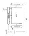
At first, the embodiment of the invention 1 is described.Fig. 1 is the figure of formation of the electro-optical device of the expression element circuit of using the embodiment of the invention 1.As shown in the drawing, in this electro-optical device, be laid with across mutually the multi-strip scanning line (S1, S2, S3 ...) and many data lines (D1, D2, D3 ...), and be respectively arranged with image element circuit 20 in its intersection everywhere, as element circuit one example of present embodiment rectangularly.
Scan line drive circuit 130, with fixed moment respectively to sweep trace S1, S2, S3 ... apply and select current potential Vsel.Data line drive circuit 140, respectively to data line D1, D2, D3 ... supply is as the data current Idata of data-signal.
In addition, in Fig. 1, omitted the power lead V of back with narration.In addition, in this explanation, sometimes the part that is laid with image element circuit 20 is also referred to as display screen rectangularly.In the present embodiment, the corresponding image element circuit 20 of a pixel that should show shows a pixel but also can constitute with a plurality of sub-pixels.
Fig. 2 (a) is the circuit diagram of expression as the concrete formation of the image element circuit 20 of the element circuit of present embodiment.In addition, the image element circuit among this figure is interleaved mode a kind of of corresponding general sweep trace S and data line D.
In the figure, being driven device L, for example, is the organic EL device that is subjected to current drives, represents with Diode symbol in the figure.This element circuit except being driven device L, also comprises the capacity cell C of driving transistors Tr1, switching transistor Tr2 (the 2nd switching transistor), switching transistor Tr3 (the 1st switching transistor), compensation transistor Tr4 and savings electric charge.Wherein, driving transistors Tr1, compensation transistor Tr4 be aging strong P channel-type thin film transistor (TFT) (Thin Film Transistor:TFT) of anti-time, and switching transistor Tr2, Tr3 are N channel-type TFT.
In addition, each transistor lets us choose up to see that to select the P channel-type still be which kind of conduction type of N channel-type, is not limited to represented situation here.And the conduction type of switching transistor Tr2, Tr3 (the N channel-type still is the P channel-type) also can be different mutually.But,, the sweep trace opposite with its logic level need be set on the basis of sweep trace S in addition, and be connected with the grid of the switching transistor of electing the P channel-type as if the conduction type that makes switching transistor Tr2, Tr3 is not mutually not simultaneously.
Be driven the end of device L, in figure, do not have the hole of expression to inject and be connected, and the other end that is driven device L is connected with negative electrode E with the drain electrode of driving transistors Tr1 with electrode.
In addition, the source electrode of driving transistors Tr1 is connected with power lead V, and its grid is connected with the end of capacity cell C, the drain electrode of switching transistor Tr4 and the drain electrode of transistor Tr 4 respectively.The other end of capacity cell C is connected with power lead V.
The drain electrode of compensation transistor Tr4 is connected with the grid of himself.Therefore, compensation transistor Tr4 is that diode-type connects.
In addition, the drain electrode of compensation transistor Tr4 and grid are connected with the end (drain electrode of the grid of driving transistors Tr1, switching transistor Tr3) of capacity cell C, and the source electrode of compensation transistor Tr4 is connected with the source electrode of switching transistor Tr2.The drain electrode of switching transistor Tr2 is connected with power lead V.The source electrode of switching transistor Tr3 is connected with data line D, and the grid of switching transistor Tr2, Tr3 is connected with sweep trace S respectively.
Below, the action of the element circuit of Fig. 2 (a) is described.Switching transistor Tr2, Tr3 are applied to the selection current potential VSEL control on the grid separately and conducting ends through sweep trace S.In the present embodiment here, because switching transistor Tr2, Tr3 are the N channel-types, so conducting respectively when selecting current potential VSEL for high level.When switching transistor Tr2, Tr3 are conducting state when data line D supplies with data current Idata, because the grid of compensation transistor Tr4 equates with source potential, so for compensation transistor Tr4,
Vgs (potential difference (PD) of grid and source electrode)=Vds (potential difference (PD) of drain electrode and source electrode)
Set up, thereby the electric charge of corresponding this state put aside in capacity cell C, the voltage between terminals of capacity cell C is applied on the grid of driving transistors Tr1.That is to say, the grid voltage of the amount controlling and driving transistor Tr 1 by the data current Idata that supplied with by data line D, thereby the magnitude of current between drain electrode-source electrode of driving transistors Tr1 is controlled, and then the letter that flows through the electric current I ds that is driven device L is controlled.
In foregoing circuit, driving transistors Tr1 and compensation transistor Tr4 have constituted so-called current mirroring circuit, the value of the electric current I ds between drain electrode-source electrode of driving transistors Tr1, just supply with the current value be driven device L, be directly proportional with the magnitude of current between drain electrode-source electrode of compensation transistor Tr4.
In addition, the electric current I ds between drain electrode-source electrode of driving transistors Tr1, and flow through the ratio of the data current Idata between drain electrode-source electrode of compensation transistor Tr4, depend on the characteristic of driving transistors Tr1 and compensation transistor Tr4.Therefore, gain constant (flowing through this transistorized magnitude of current when applying certain voltage on transistorized grid and source electrode) by making one of characteristic as driving transistors Tr1 and compensation transistor Tr4 is consistent, can make the electric current I ds that flows through driving transistors Tr1, consistent with the data current Idata that flows through compensation transistor Tr4.Particularly in the present embodiment, because the drain electrode of compensation transistor Tr4 is direct-connected with the grid of driving transistors Tr1, so by the data current Idata of compensation transistor Tr4, directly reflect the electric current I ds that is controlled by driving transistors Tr1, thereby can improve the consistance of the two.
Therefore, if when making the gain constant of driving transistors Tr1 and compensation transistor Tr4 as one man constitute display screen, even the formed driving transistors Tr1 of pixel of corresponding each display screen is variant, what also can be comprised in each pixel of display screen is driven the electric current I ds that device L supplies with identical size.Therefore, can suppress the caused luminance difference of characteristic heterogeneity because of driving transistors Tr1.
Such as everyone knows, in the manufacture process that contains the display screen that is driven device L, making the characteristics of transistor of closing on consistent with each other is to be relatively easy to.In aforesaid present embodiment, the grid of the drain electrode of compensation transistor Tr4 and driving transistors Tr1 has been close to direct-connected degree.Therefore, in same image element circuit, make driving transistors Tr1 consistent with the gain constant of compensation transistor Tr4, not difficult, thereby, make the few display screen ratio of luminance difference and be easier to.
In addition, in the present embodiment, though the corresponding data current Idata that is supplied with by data line drive circuit 140 of the grid voltage of driving transistors Tr1 sets, but because driving transistors Tr1 and compensation transistor Tr4 have constituted so-called current mirroring circuit, so can suppress change, thereby also can play the purpose of stabilizing circuit because of the electric current I ds between drain electrode-source electrode of caused driving transistors Tr1 such as temperature variation.
In the circuit of Fig. 2 (a), make compensation transistor Tr4 between switching transistor Tr2 and switching transistor Tr3, but shown in Fig. 2 (b), also can make it between switching transistor Tr2 and power lead V.In addition, in this circuit, electric current I ds between drain electrode-source electrode of driving transistors Tr1, also same with the circuit shown in Fig. 2 (a), depend on the data current Idata that flows through compensation transistor Tr4.
Fig. 3 is the sequential chart that is used to illustrate element circuit action shown in Figure 2.
-at first, the selection current potential VSEL that makes scan line drive circuit 130 supply with sweep trace S is a high level, and make data line drive circuit 140 supply with data current Idata to data line D.
When selecting current potential VSEL to be high level, because switching transistor Tr2, Tr3 all become conducting state, so data current Idata is along power lead V, switching transistor Tr2, compensation transistor Tr4, switching transistor Tr3 and this path flow of data line D.
Mutually should data current Idata, the grid voltage of driving transistors Tr1 is determined, thereby by power lead V supply with mutually should grid voltage electric current I ds make and be driven device L luminous the time, this grid voltage is kept by capacity cell C.Therefore, even select current potential VSEL to become low level and make switching transistor Tr2, Tr3 all become cut-off state, the electric current I ds of the corresponding grid voltage that keeps still can continue to flow into and be driven among the device L, thereby the luminance that is driven device L is maintained to selects current potential VSEL to become till the high level once more next time.
But, constitute the driving transistors Tr1 of current mirroring circuit and the gain constant of compensation transistor Tr4, be not limited to aforesaid its consistent situation that makes, various requirement such as the size of display screen that can this element circuit of respective application and sweep frequency is suitably set.
For example, also can constitute the gain constant that makes compensation transistor Tr4, greater than the gain constant of driving transistors Tr1.According to this formation, owing to flow through the electric current I data of compensation transistor Tr4, can be greater than the electric current I ds that flows through driving transistors Tr1, so can shorten the required time of electric charge accumulation in capacity cell C.Therefore, can solve the high-frequencyization of the required sweep frequency of the increase of the pixel quantity of following display screen or large scaleization.
In contrast, also can constitute the gain constant that makes compensation transistor Tr4, less than the gain constant of driving transistors Tr1.According to this formation, owing to depend on the data current Idata of compensation transistor Tr4, can be less than the electric current I ds that depends on driving transistors Tr1, so the electric power that is consumed can be suppressed at electric charge accumulation among the capacity cell C time.
In addition, in Fig. 2 (a) or Fig. 2 (b),, has the formation that is connected with same sweep trace S mutually with the switching transistor Tr2 of the image element circuit 20 of delegation, the grid of Tr3.But be not limited to this formation, also can constitute the sweep trace different with sweep trace S is set, that is to say, corresponding each row is provided with two sweep traces, and makes the grid of switching transistor Tr2, Tr3 and different mutually sweep trace S connections.At this, if two kinds of formations are compared, last formation (corresponding each row image element circuit 20 has the formation of a sweep trace) constitutes (corresponding each row image element circuit 20 has the formation of two sweep traces) and compares with back one, owing to have less required wiring zone to get final product, so improve aperture opening ratio easily by guaranteeing that effective optical area determines.
Below, the manufacture process of TFT in the manufacture process of above-mentioned image element circuit 20 and pixel is described.
At first, on glass substrate, by using SiH
4PECVD or use Si
2H
6LPCVD, when forming amorphous silicon,, make this amorphous silicon polycrystallization by laser radiation or solid state growths such as excimer laser, form polysilicon layer 2 (with reference to Fig. 4 (a)).
Polysilicon layer 2 is graphical, and after forming gate insulating film 3, and then form grid 4 (with reference to Fig. 4 (b)).
Then, grid 4 is used as mask, integrates by self impurity such as phosphorus or boron are mixed polysilicon layer 2, form transistor 5a, 5b.In addition, here, the conductivity type of transistor 5a, 5b is respectively P type and N type.After forming the 1st interlayer dielectric 6, open the node hole, and then form the source electrode and 7 (with reference to Fig. 4 (c)) that drain.
Then, form the 2nd interlayer dielectric 8 after, open the node hole, and then form the pixel electrode 9 (with reference to Fig. 4 (d)) that forms by ITO (IndiumTin Oxide).
Be close to layer 10 by formation and make it cover the 2nd interlayer dielectric 8 and the pixel electrode 9 that forms like this, corresponding light-emitting zone forms peristome.And then, cambium layer interbed 11, same corresponding light-emitting zone forms peristome (with reference to Fig. 5 (a)).
Then, by oxygen plasma or CF
4Plasma treatment such as plasma, the wettability on control basal plate surface.Then, form hole injection layer 12 and luminescent layer 13 respectively by liquid phase processing or application of vacuum.In addition, handle, can enumerate spin coated, squeegee coating, inkjet process etc., and against vacuum is handled, and can enumerate sputter and evaporation etc. for liquid phase.Follow again, form the negative electrode 14 that contains metals such as aluminium.At last, form sealant 15, finish organic EL device (with reference to Fig. 5 (b)).
At this, the effect of being close to layer 10 is to improve the exposure level of substrate and interlevel layer 11 and obtain the accurate light emission area.In addition, the effect of interlevel layer 11 is, thereby makes negative electrode 14 away from grid 4, source electrode and drain and 7 reduce stray capacitances and handle when forming hole injection layer 12 and luminescent layer 13 by liquid phase, and the wettability of control surface makes it can carry out correct figure and forms.In addition, electron supplying layer (not expression among the figure) also can be set on luminescent layer 13.
(embodiment 2)
In the foregoing description 1, for example, by making driving transistors Tr1 identical with the gain constant of compensation transistor Tr4, can make the electric current I ds between drain electrode-source electrode of driving transistors Tr1, consistent with the data current Idata between the drain electrode-source electrode that flows through compensation transistor Tr4.Therefore, even aspect driving transistors Tr1, produce property difference, also can be to the electric current I ds that device L supplies with identical size that is driven of all pixels, thereby can suppress because of the caused uneven luminance of the property difference of driving transistors.
But, in embodiment 1, by among Fig. 2 (a) or Fig. 2 (b) as can be seen, in an image element circuit, need four transistors altogether.Therefore, from the angle of display screen, cause decrease in yield of respective transistor quantity part and aperture opening ratio to descend easily.
Therefore, on the basis of the caused brightness irregularities of property difference that suppresses driving transistors Tr1, the embodiment 2 that can reduce required transistor number in the pixel describes below.
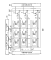
Fig. 6 represents the block scheme of formation of OLED display of the element circuit of Application Example 2.
As shown in the drawing, OLED display 100 comprises: signal generating circuit 110, display screen portion 120, scan line drive circuit 130, data line drive circuit 140 and power source line control circuit 150.
Signal generating circuit 110 in the OLED display 100, scan line drive circuit 130, data line drive circuit 140 and power source line control circuit 150 also can be made of independent electronic component respectively.For example, signal generating circuit 110, scan line drive circuit 130, data line drive circuit 140 and power lead driving circuit 150 also can be made of the monolithic semiconductor integrated circuit device respectively.In addition, signal generating circuit 110, scan line drive circuit 130, data line drive circuit 140, and power source line control circuit 150 in all or part of, also can constitute, and the program by writing this IC chip realizes its function with the method for software by programmable I C chip.
Signal generating circuit 110, the view data according to from the external device (ED) that does not have expression among the figure makes the scan control signal and the data controlling signal that are used for display image in display screen portion 120.And signal generating circuit 110 is in the time of the described scan control signal of scan line drive circuit 130 outputs, to the described data controlling signal of data line drive circuit 140 outputs.In addition, signal generating circuit 110 is to power source line control circuit 150 output timing controling signals.
Fig. 7 is expression display screen portion 120 and the data line drive circuit 140 inner figure that constitute.As shown in the drawing, display screen portion 120 is at the M bar data line Xm (m=1~M of correspondence along the column direction extension; M is an integer), with the N bar sweep trace Yn (n=1~N that follows the direction extension; N is an integer) the position of cross part, have image element circuit 200 respectively as element circuit.That is to say, each image element circuit 200, by respectively with the data line Xm that extends along column direction, and follow the sweep trace Yn that direction extends and be connected, be arranged in rectangular formation electronic circuit.
In addition, in every row, follow direction (sweep trace extend direction) respectively and be provided with the 1st power lead L1 and the 2nd power lead L2.
Image element circuit 200, comprise with embodiment 1 in be driven the same organic EL device of device L 210.The image element circuit 200 of 1 row part and is connected the 1st power lead L1 and the 2nd power lead L2 that should go.That is to say the image element circuit 200 of 1 row part, shared the 1st power lead L1 and the 2nd power lead L2 mutually.
At this, the 1st power lead L1 of each row is connected with voltage supply line VL respectively indirectly through transistor Q, and the 2nd power lead L2 of each row directly is connected with voltage supply line VL respectively, supplies with driving voltage Vdd thereby constitute to image element circuit 200.
Scan line drive circuit 130, the corresponding scan control signal of being exported by signal generating circuit 110, a rule is selected sweep trace in order in multi-strip scanning line Yn, and selected sweep trace is supplied with the sweep signal of representing this selection.
Data line drive circuit 140 has 230, one line drives 230 of line drive of corresponding each bar data line, and is connected with an end of its corresponding data line.At this, line drive 230 according to the data controlling signal of being exported by signal generating circuit 110, generates data current Idata, and supplies with corresponding data lines.
In general, the line drive 230 of m row when selecting the capable sweep trace Yn of n, in the data line Xm of m row, is supplied with the data current Idata of brightness that indication comprises the organic EL device 210 of the image element circuit 200 that is positioned at the capable m row of n.
In addition, in image element circuit 200, as the back will be narrated, when the data current Idata of corresponding supply on corresponding data line sets internal state, constitute mutually and should control the drive current Ids that supplies to organic EL device 210 by internal state.
Power source line control circuit 150, to the power lead control line F supply power line control signal that is located at each row, the conducting of controlling each row transistor Q ends respectively.Particularly, power source line control circuit 150, according to the scan control signal of being exported by signal generating circuit 110, generate the power lead control signal of certain row, make its sweep signal in full accord with the selection of the sweep trace of representing this row, and, make its selection mode have part to repeat in time, and supply with power lead control line F going.
Fig. 8 is the circuit diagram of expression as the concrete formation of the image element circuit 200 of the element circuit of embodiment 2.In the figure, show in each image element circuit 200 infall of the data line Xm of sweep trace Yn that corresponding n is capable and m row.
As shown in Figure 8, image element circuit 200 comprises three transistors and a capacity cell.Specifically, image element circuit 200 comprises driving transistors Trd, compensation transistor TrC, switching transistor Trs and as the maintenance electricity consumption container C 1 of capacity cell.
In addition, in the present embodiment, the conduction type of driving transistors Trd and compensation transistor TrC is respectively P type (P raceway groove), and the conduction type of switching transistor Trs is N type (a N raceway groove), but for the selection of these conduction types, the situation shown in being not limited to here.In addition, the transistor in the image element circuit 200 is formed by TFT (thin film transistor (TFT)) usually.
The drain electrode of driving transistors Trd (the 1st terminal), with by and the anode of El element 210 be connected.The plus earth of organic EL device 210.The source electrode of driving transistors Trd (the 2nd terminal) is connected with the 2nd power lead L2.The 2nd power lead L2 is connected with the voltage supply line VL of the right-hand member that is arranged on display screen portion 120.The grid of driving transistors Trd (the 1st grid), N is connected with contact.In addition, contact N refers to, the tie point of the drain electrode of the grid of driving transistors Trd, an end that keeps electricity consumption container C 1, switching transistor Trs and the drain electrode of compensation transistor TrC.The other end that keeps electricity consumption container C 1, with the source electrode of driving transistors Trd, just the 2nd power lead L2 connects.
The drain electrode of switching transistor Trs (the 6th terminal), Xm is connected with data line, its drain electrode (the 5th terminal), N is connected with contact.In addition, the grid of switching transistor Trs, Yn is connected with sweep trace.Therefore, when in sweep trace Yn, supply with when representing the selecteed sweep signal of this sweep trace Yn (when becoming high level), switching transistor Trs becomes conducting state.
On contact N, not only be connected with the drain electrode (the 3rd terminal) of compensation transistor TrC, also be connected with its grid.In addition, the source electrode of compensation transistor TrC (the 4th terminal) is connected with the 1st power lead L1.Therefore, compensation transistor TrC, played from the 1st power lead L1 to the effect of contact N as the diode of direction of passage.
In addition, in each image element circuit 200, arrange the transistor that forms, form by TFT (thin film transistor (TFT)) usually.
The 1st power lead L1 is connected with voltage supply line VL through the transistor Q as control circuit.And the 1st power lead L1 and the 2nd power lead L2 constitute power lead L.
The grid of transistor Q, F is connected with the power lead control line.Transistor Q, corresponding through power lead control line F, by the power lead control signal that power source line control circuit 150 is supplied with, become a kind of state in disconnected state (cut-off state) of TURP or the status of electrically connecting (conducting state).Because the conduction type of transistor Q is P type (a P raceway groove), so when the power lead control signal was low level, transistor Q became conducting state.
Secondly, with reference to Fig. 9 the driving method of the image element circuit 200 of OLED display 100 is described.Fig. 9 is used to illustrate this driving method sequential chart.
At first, TrP during data write, when supplying with the sweep signal of the selection of representing sweep trace Yn by scan line drive circuit 130 (when sweep trace Yn is high level), switching transistor Trs is a conducting state.Cooperate the supply of this sweep signal owing to supply with the low level power line control signal make transistor Q conducting to power lead control line F, so during data write TrP, transistor Q also becomes conducting state.
Therefore, electric current is along voltage supply line VL, transistor Q, the 1st power lead L1, compensation transistor TrC, switching transistor Trs and this path flow mistake of data line Xm.At this moment the electric current that flows through, the data current Idata that is generated by line drive 230 exactly just indicates the data current Idata of the brightness of organic EL device 210 in the image element circuit 200 of the capable m row of n.
And, on contact N, produce the voltage VC1 of the corresponding data current Idata that at this moment flows through, when being held electricity consumption container C 1 and keeping, be applied to the grid of driving transistors Trd.Therefore, drive current Ids flows through driving transistors Trd, thereby makes organic EL device 210 beginnings luminous.
Then, TrP finishes during data write, and when arriving between light emission period TEL, sweep trace Yn becomes low level.Therefore, switching transistor Trs becomes cut-off state.The state variation that cooperates this sweep signal is because the power lead control signal becomes high level, so transistor Q also becomes cut-off state.Even switching transistor Trs and transistor Q become cut-off state, because on the grid of driving transistors Trd, be applied with by the voltage VC1 that keeps electricity consumption container C 1 to be kept, so the luminance of organic EL device 210, can be maintained to next time always sweep trace Yn selected once more till (transistor Q conducting till) once more.
And This move in each circuit of the image element circuit 200 of delegation's part of corresponding sweep trace Yn, also carries out respectively simultaneously.In addition, from image element circuit 200 on the whole, be by the 1st, 2,3 ..., sweep trace that N is capable carries out in proper order.
In addition, TEL formation drive cycle Tc between TrP and light emission period during data write.This drive cycle Tc is meant that the brightness of organic EL device 210 once connects the cycle meaning that once is updated, and is equivalent in meaning with so-called image duration (vertical scanning period).
In order to be briefly described the action mechanism of above-mentioned image element circuit, if when considering that compensation is gone forward side by side line display with the threshold voltage VTH2 of transistor Tr C, the current potential Vn of described contact N, can be expressed as and be created in the voltage VC1 that keeps electricity consumption container C 1, and by deducting compensation among the driving voltage Vdd with value (Vn=Vdd-Vth2) the sum compensation of the threshold voltage VTH2 of transistor Tr C value (Vn=Vdd-Vth2) sum with the threshold voltage VTH2 of transistor Tr C.That is to say, can represent with following formula (1).
Vg=VC1+Vdd-Vth2 ……(1)
The grid-source voltage Vgs of driving transistors Trd, owing to be its grid potential Vg and poor (Vg-Vs) that drive with the source potential Vs (equaling Vdd) of transistor Tr d, so drive transistor gate-voltage between source electrodes Vgs can be expressed as following formula (2).
Vgs=Vg-Vs ……(2)
In this formula (2), when Vg shown in the substitution formula (1) and Vs (equaling Vdd), can obtain following formula (3).
Vgs=VC1+Vdd-Vth2-Vdd
=VC1-Vth2 ……(3)
At this, if make the threshold voltage vt h2 of compensation transistor TrC as mentioned above, during with the threshold voltage vt h1 approximately equal of driving transistors Trd, voltage Vgs between the gate-to-source of expression can be expressed as following formula (4) in the formula (3).
Vgs=VC1-Vth1 ……(4)
And flow through electric current I ds between source electrode-drain electrode of driving transistors Trd, can be expressed as following formula (5).
Ids=(1/2)β(-Vgs-Vth1)
2 ……(5)
β in this formula is a gain constant, can be expressed as
β=(μAW/L)。
Wherein, μ is a carrier mobility, and A is a grid capacitance, and W is a channel width, and L is that channel is long.
When the Vgs substitution in the formula (4) is made (5),
Ids=(1/2)β(-VC1+Vth1-Vth1)
2
=(1/2)β(-VC1)
2 ……(6)
From formula (6), as can be seen, flow through the electric current I ds between source electrode-drain electrode of driving transistors Trd, only depend on to be created in the voltage VC1 that keeps on the electricity consumption container C 1.
In general, mutually close transistorized threshold property etc. is tending towards always than being easier to.Therefore, because this extremely close compensation transistor TrC of similar same image element circuit and the threshold voltage characteristic of driving transistors Trd are reached unanimity also than being easier to, so can make the electric current I ds that flows through organic EL device 210, be not subjected to the influence of the threshold voltage characteristic of driving transistors Trd, and depend on data current Idata.
That is to say, in embodiment 2, because the drain electrode of compensation transistor TrC directly is connected with the grid of driving transistors Trd, so result that it is close, when two characteristics of transistor are reached unanimity, make data current Idata, directly be reflected among the electric current I ds that is controlled by driving transistors Trd, and can improve the consistance of the two by compensation transistor.
Therefore, in each image element circuit 200 in display screen portion 120, even produce the threshold voltage difference of driving transistors Trd because of heterogeneity, owing to can the electric current I ds that flow through organic EL device 210 not exerted an influence, so same with described embodiment 1, also can suppress by the caused brightness irregularities of the property difference of driving transistors.
Have, in embodiment 2, being formed on a transistor in the image element circuit 200 is three again, compares with four of the image element circuit 20 of embodiment 1, can reduce one.Therefore, according to embodiment 2, except suppressing to prevent by the bad caused decrease in yield of transistor by the caused brightness irregularities this point of the property difference of driving transistors, and by guaranteeing to be equivalent to the aperture area of a pixel, thereby can improve aperture opening ratio.
In addition, in embodiment 2, also can carry out suitable setting similarly to Example 1.For example, also can make the gain constant of compensation transistor TrC, constitute gain constant greater than driving transistors Trd.According to this formation, owing to flow through the electric current I data of compensation transistor TrC, greater than the electric current I ds that flows through driving transistors Trd, so can shorten the required time of savings electric charge in capacity cell C.Therefore, can be at the high-frequencyization of the required sweep frequency of the increase of the pixel quantity of following display screen or large scaleization.
In contrast, also can make the gain constant of compensation transistor TrC, constitute gain constant less than driving transistors Trd.According to this formation, owing to depend on the data current Idata of compensation transistor TrC, less than the electric current I ds that depends on driving transistors Trd, so the power consumption can be reduced in the electric charge savings of capacity cell C the time.
In embodiment 2, though preferably switch is set at transistor Tr s and transistor Q, TrP is conducting state during data write, and TEL is cut-off state between light emission period, is not particularly limited in this.In addition, though drive current Ids is set at, TrP does not flow through organic EL device 210 during data write, and TEL flows through between light emission period, is not particularly limited in this.
Channel width by making compensation transistor TrC etc. is greater than driving transistors Trd's, compare with measure-alike the making of driving transistors Trd and compensation transistor TrC, owing to when supplying with the data of low gray scale, also can utilize high relatively electric current, so can suppress to postpone by the action that stray capacitance etc. causes as data current Idata.
In addition, in image element circuit 200, preferably the threshold voltage VTH1 of driving transistors Trd is set at threshold voltage VTH2, but is not particularly limited in this greater than compensation transistor TrC.For example, when making organic EL device 210 TrP is also luminous during data write, also the threshold voltage VTH1 of driving transistors Trd can be set at threshold voltage VTH2 less than compensation transistor TrC.
In addition, the supply power line control signal during with supply with sweep signal during be set in time completely or partially overlapping.Just, during writing with data TrP much at one during transistor Q is set at conducting state.But, by before the sweep signal of supplying with the selection of representing sweep trace, supplying with the power lead control signal that makes transistor Q conducting, can obtain the driving situation of the grid voltage of transistor Tr d that desired inhibition is set by data current Idata sometimes with driving voltage Vdd variation.
In addition, in Fig. 7, it is the right-hand member that voltage supply line VL is arranged on display screen portion 120, but be not limited thereto, for example, also can be arranged on the left end of display screen portion 120, in addition, though with transistor Q and voltage supply line VL, separate formation separately, also can be arranged on power source line control circuit 150 inside with power source line control circuit 150.
Have, though transistor Q is used as control circuit, place of transistor Q also can be provided with the switch that can switch between electronegative potential and noble potential again.In order to improve the driving force of driving transistors Trd, also can adopt voltage follower circuit that comprises buffer circuit or source follower circuit etc., fully reduce the impedance of the 2nd power lead L2 or voltage supply line VL.
(application of embodiment 2)
In display screen shown in Figure 7, for the purpose of simplifying the description, the example that carries out the gray scale demonstration with monochrome is illustrated, but when being considered as the function of actual display screen, needing to carry out colour sometimes and show.Therefore, as the application examples of embodiment 2, describe being used for the colored electro-optical device that shows.
Figure 10 is the block scheme of formation of the electro-optical device of this application examples of expression.In addition, the electro-optical device among Figure 10 is the OLED display that adopts as the organic EL device of electrooptics device, for Fig. 7 in identical component part used identical symbol, and omit its detailed description.
In Figure 10, display screen portion 120 is made of with image element circuit 200B with image element circuit 200G and indigo plant with organic EL device 210 of radiation blue light with image element circuit 200R, the green of organic EL device 210 with radiation green light the red of the organic EL device 210 with radiation red light.
At this, in display screen portion 120, the 1st row is laid the red image element circuit 200R that uses, and the 2nd row is laid the green image element circuit 200G that uses, and the 3rd row is laid the blue image element circuit 200B that uses, and the 4th row is laid the red image element circuit 200R that uses, and afterwards, repeats this laying state.That is to say that the image element circuit of same color is laid delegation's part along the direction that extends of sweep trace, and, the homochromy image element circuit of delegation's part, dual-purpose sweep trace, the 1st power lead L1 and the 2nd power lead L2.
In addition, image element circuit 200R, 200G of all kinds, the circuit of 200B constitute, and constitute identical with the circuit of image element circuit 200 shown in Figure 8 respectively.
Voltage supply line in this application examples is for the driving voltage of supplying with every kind of color specific is provided with three.That is to say that voltage supply line VLR supplies with red driving voltage VddR with image element circuit 200R, voltage supply line VLG supplies with green driving voltage VddG with image element circuit 200G, and voltage supply line VLB supplies with blue driving voltage VddB with image element circuit 200B.
In addition, follow direction respectively, every row is provided with the 1st power lead L1 and the 2nd power lead L2.At this, correspondence is positioned at red the 1st power lead L1 with image element circuit 200R with delegation, be connected with voltage supply line VLR indirectly through transistor QR, when this transistor QR conducting, supply with driving voltage VddR, and the 2nd power lead L2, VLR directly is connected with voltage supply line, often supplies with driving voltage VddR.
For green image element circuit 200G and the blue image element circuit 200B that uses of using that is positioned at delegation, also respectively with red identical with image element circuit 200R.That is to say, correspondence is positioned at green the 1st power lead L1 with image element circuit 200G with delegation, when this transistor QG conducting, supply with driving voltage VddG, and the 2nd power lead L2 often supplies with driving voltage VddG, in addition, correspondence is positioned at the 1st power lead L1 that uses image element circuit 200B with the indigo plant of delegation, when this transistor QB conducting, supply with driving voltage VddB, and the 2nd power lead L2 often supplies with driving voltage VddB.
Below, image element circuit 200R, 200G in the electro-optical device of application examples, the driving method of 200B are described.
At first, when the sweep trace Y1 that selects the 1st row also supplies with the sweep signal of representing this message (when sweep trace Y1 is high level), at each red image element circuit 200R that uses that is arranged in the 1st row, switching transistor Trs becomes conducting state.Cooperate the supply of this sweep signal, because the power lead control signal of the 1st row becomes low level, so the transistor QR of the 1st row also becomes conducting state.
Have again, cooperate the supply of this sweep signal, indicate the data current Idata of the brightness of the organic EL device 210 among the 1st image element circuit 200R that goes, supply to the data line of each row respectively.
Therefore, in each image element circuit 200R of the 1st row,, can keep the grid voltage of driving transistors Trd by the electric charge of savings corresponding data electric current I data in keeping electricity consumption container C 1.Thereby, driving transistors Trd, beginning is supplied with drive current Ids that should grid voltage with organic EL device 210 to red, thereby makes red luminous with organic EL device 210 beginnings.
Then, when the sweep trace Y2 that selects the 2nd row also supplies with the sweep signal of representing this message (when sweep trace Y2 is high level), at each green image element circuit 200G that uses that is arranged in the 2nd row, switching transistor Trs becomes conducting state.Cooperate the supply of this sweep signal, because the power lead control signal of the 2nd row becomes low level, so the transistor QG of the 2nd row also becomes conducting state.
Cooperate the supply of this sweep signal, indicate the data current Idata of the brightness of the organic EL device 210 among the 2nd image element circuit 200G that goes, supply to the data line of each row respectively.
Therefore, in each image element circuit 200G of the 2nd row,, can keep the grid voltage of driving transistors Trd by the electric charge of savings corresponding data electric current I data in keeping electricity consumption container C 1.Thereby, driving transistors Trd, beginning is supplied with drive current Ids that should grid voltage with organic EL device 210 to green, thereby makes green luminous with organic EL device 210 beginnings.
In addition, when selecting the 2nd horizontal scanning line Y2, in each image element circuit 200R of the 1st row, though switching transistor Trs and transistor QR become cut-off state, but its driving transistors Trd, owing to supply with the drive current Ids of the corresponding grid voltage that is kept by maintenance electricity consumption container C 1 with organic EL device 210, so red luminance with organic EL device 210 will be kept to red.
Secondly, when the sweep trace Y3 that selects the 3rd row also supplies with the sweep signal of representing this message (when sweep trace Y3 is high level), at each indigo plant image element circuit 200B that is arranged in the 3rd row, switching transistor Trs becomes conducting state.Cooperate the supply of this sweep signal, because the power lead control signal of the 3rd row becomes low level, so the transistor QB of the 3rd row also becomes conducting state.
Cooperate the supply of this sweep signal, indicate the data current Idata of the brightness of the organic EL device 210 among the 3rd image element circuit 200B that goes, supply to the data line of each row respectively.
Therefore, in each image element circuit 200B of the 3rd row,, can keep the grid voltage of driving transistors Trd by the electric charge of savings corresponding data electric current I data in keeping electricity consumption container C 1.Thereby, driving transistors Trd, beginning is supplied with drive current Ids that should grid voltage with organic EL device 210 to indigo plant, thereby makes blue luminous with organic EL device 210 beginnings.
In addition, when selecting the 3rd horizontal scanning line Y3, in each image element circuit 200G of the 2nd row, though switching transistor Trs and transistor QG become cut-off state, but its driving transistors Trd, owing to supply with the drive current Ids of the corresponding grid voltage that is kept by maintenance electricity consumption container C 1 with organic EL device 210, so green luminance with organic EL device 210 will be kept to green.
Subsequent, identical action the 4th, 5,6 ..., after the N behavior only repeats in order, select the 1st horizontal scanning line Y1 once more, data (correspondence is accumulated in the electric charge that keeps the data current Idata in the electricity consumption container C 1) will be rewritten.
The OLED display 100 of this application examples also can obtain effect similarly to Example 2.
In general, the luminescence efficiency of red, green, blue organic EL device 210 is different mutually, for driving voltage, and sometimes also need be at every kind of color settings optimum value.In the formation of application examples, because whole-colored image element circuit is laid in in the delegation, and shared the 1st power lead L1 and the 2nd power lead L2 supply with driving voltage by every kind of color, so than being easier at every kind of color settings optimal drive voltage.In addition, because of the organic EL device 210 long-term luminous deteriorations etc. that cause, also have when need set driving voltage once more at every kind of color, but in application examples, the setting again of this driving voltage at every kind of color is also than being easier to.
In addition, in aforesaid embodiment 1,2 and application examples thereof, for the example of image element circuit, but also can be applied to (particularly MRAM) memory storages such as RAM as element circuit (electronic circuit).In addition, enumerated the example of organic EL device, but also can be that inorganic El element also can be LED or FED as being driven device.Even also can be senser elements such as light detecting device.
(e-machine)
Below, application is comprised several situations in the e-machine of electro-optical device of element circuit of embodiment 1,2 and application examples thereof describe.
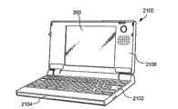
Figure 11 is the stereographic map that the portable personal computer formation of this electro-optical device is used in expression.As shown in the drawing, comprise the electro-optical device 300 of the element circuit of embodiment, be used as the display unit of personal computer 2100.In addition, on the main body 2104 of personal computer 2100, has keyboard 2102.
Figure 12 is the stereographic map that the portable telephone formation of above-mentioned electro-optical device 300 is used in expression.In the figure, portable telephone 2200 except having a plurality of action buttons 2202, also has receiving mouth 2204, mouth piece 2206, and electro-optical device recited above 300.
Figure 13 is the stereographic map of formation that expression is applied to above-mentioned electro-optical device 300 digital camera of view finder.The silver halide photography machine be that the light image by subject makes light reaching the film, and digital camera 2300 is by CCD picture pick-up devices such as (Charge Coupled Device) subject to be carried out light-to-current inversion to generate and store image pickup signal.At this, the back side in the main body 2302 of digital camera 2300 is provided with aforesaid electro-optical device 300.This electro-optical device 300 is because of corresponding image pickup signal shows, so can play the effect of the view finder that shows subject.In addition, on the front (back side among Figure 13) of main body 2302, be provided with the light receiving unit 2304 that comprises optical lens and CCD etc.
When the cameraman confirms to be presented at shot object image in the electro-optical device 300, and when pressing shutter 2306, corresponding this CCD image pickup signal constantly just is transferred and stores in the storer of circuit board 2308.
In addition, on the side of the shell 2302 of this digital camera 2300, be provided with and be used to implement outside video signal displayed lead-out terminal 2312 and data communication with input and output terminal 2314.
In addition, as the e-machine of using above-mentioned electro-optical device, except personal computer shown in Figure 11, portable telephone shown in Figure 12, and digital camera shown in Figure 13, the machine etc. that can also enumerate liquid crystal TV set, find a view type or monitor type video camera, automobile navigation apparatus, pager, electronic memo, counter, word processor, workstation, videophone, point of sells terminal and have the touch operation screen.And, as the display part of these various e-machines, undoubtedly, electro-optical device that can Application Example.
In sum, can accomplish, not be subject to the influence ground of the difference of driving transistors, be driven device, supply with electric current as target to current modes such as similar organic EL devices by the present invention.