CN100406935C - Optimized multi-layer optical waveguiding system - Google Patents
Optimized multi-layer optical waveguiding system Download PDFInfo
- Publication number
- CN100406935C CN100406935C CN028091973A CN02809197A CN100406935C CN 100406935 C CN100406935 C CN 100406935C CN 028091973 A CN028091973 A CN 028091973A CN 02809197 A CN02809197 A CN 02809197A CN 100406935 C CN100406935 C CN 100406935C
- Authority
- CN
- China
- Prior art keywords
- cushion
- sandwich layer
- refractive index
- core
- polymerization
- Prior art date
- Legal status (The legal status is an assumption and is not a legal conclusion. Google has not performed a legal analysis and makes no representation as to the accuracy of the status listed.)
- Expired - Fee Related
Links
Images


Classifications
-
- G—PHYSICS
- G02—OPTICS
- G02B—OPTICAL ELEMENTS, SYSTEMS OR APPARATUS
- G02B6/00—Light guides; Structural details of arrangements comprising light guides and other optical elements, e.g. couplings
- G02B6/02—Optical fibres with cladding with or without a coating
-
- G—PHYSICS
- G02—OPTICS
- G02B—OPTICAL ELEMENTS, SYSTEMS OR APPARATUS
- G02B6/00—Light guides; Structural details of arrangements comprising light guides and other optical elements, e.g. couplings
- G02B6/10—Light guides; Structural details of arrangements comprising light guides and other optical elements, e.g. couplings of the optical waveguide type
- G02B6/12—Light guides; Structural details of arrangements comprising light guides and other optical elements, e.g. couplings of the optical waveguide type of the integrated circuit kind
- G02B6/122—Basic optical elements, e.g. light-guiding paths
- G02B6/1221—Basic optical elements, e.g. light-guiding paths made from organic materials
-
- G—PHYSICS
- G02—OPTICS
- G02B—OPTICAL ELEMENTS, SYSTEMS OR APPARATUS
- G02B6/00—Light guides; Structural details of arrangements comprising light guides and other optical elements, e.g. couplings
- G02B6/10—Light guides; Structural details of arrangements comprising light guides and other optical elements, e.g. couplings of the optical waveguide type
- G02B6/12—Light guides; Structural details of arrangements comprising light guides and other optical elements, e.g. couplings of the optical waveguide type of the integrated circuit kind
- G02B6/13—Integrated optical circuits characterised by the manufacturing method
-
- G—PHYSICS
- G02—OPTICS
- G02B—OPTICAL ELEMENTS, SYSTEMS OR APPARATUS
- G02B6/00—Light guides; Structural details of arrangements comprising light guides and other optical elements, e.g. couplings
- G02B6/10—Light guides; Structural details of arrangements comprising light guides and other optical elements, e.g. couplings of the optical waveguide type
- G02B6/12—Light guides; Structural details of arrangements comprising light guides and other optical elements, e.g. couplings of the optical waveguide type of the integrated circuit kind
- G02B2006/12083—Constructional arrangements
- G02B2006/12107—Grating
-
- G—PHYSICS
- G02—OPTICS
- G02B—OPTICAL ELEMENTS, SYSTEMS OR APPARATUS
- G02B6/00—Light guides; Structural details of arrangements comprising light guides and other optical elements, e.g. couplings
- G02B6/10—Light guides; Structural details of arrangements comprising light guides and other optical elements, e.g. couplings of the optical waveguide type
- G02B6/12—Light guides; Structural details of arrangements comprising light guides and other optical elements, e.g. couplings of the optical waveguide type of the integrated circuit kind
- G02B2006/12166—Manufacturing methods
- G02B2006/12176—Etching
Abstract
A single mode optical waveguide which is lithographically formed and employs polymeric materials having low propagation loss. The optical waveguide has a substrate (2), a polymeric buffer layer (4) having an index of refraction nb disposed on a surface of the substrate, a patterned, light-transmissive core layer (8) having an index of refraction nc disposed directly on a surface of the cladding layer, and an overcladding layer (10) having an index of refraction no on a top surface of the core, side walls of the core, and exposed portions of the buffer layer, with nb<no<nc and - = nc - no.
Description
Background of invention
Invention field
The present invention relates to plane or " integrated " optical waveguide, relate in particular to the single mode waveguide of the lithography formation of using organic and polymeric material.
Background technology
The multilayer lightguide structure is used to constitute integrated optical circuit to send and to control the light signal in the optical fiber telecommunications system.In optical communication system, signal passes through the carrier wave of use such as laser and LED source generation with the infrared light frequency transmission.These optical communication systems are favourable to be because they provide some advantages with respect to the electronic communication system that uses copper cash or concentric cable.They have the communication channel number that improves greatly, reach the ability with the speed transmission signals higher than electronic system.
The invention relates to the formation of the fiber waveguide device of printing opacity.The operation of optical waveguide is based on such fact, promptly when the core medium of optical transparency by another have than the clad medium of low-refraction around or when otherwise meeting the boundary, the light of introducing along core medium axle by high reflection, therefore produces photoconductive effect at the boundary of the clad medium that centers on.
Might produce polymeric optical waveguide and other optical device by light path or optical networking transmitting optical signal.A kind of method that is used to form fiber waveguide device comprises the application standard photoetching process.Photopolymer is particularly advantageous in optical application, because they can form pattern by photoetching technique commonly known in the art.Chance simpler, the more rational manufacturing process of cost that photopolymer also provides.Imprint lithography is used for determining to be deposited on the pattern of the photosensitive layer that contains photopolymer on the substrate.This layer itself can be made up of several layers that the identical or different polymeric material with different refractivity is formed, to form core, to go up clad and following clad or structural member.
In many known photopolymers, the acrylate material has been determined and has been suitable for optical waveguide is because it is optical transparency, low-birefringence, and obtains the monomer of wide region easily.
Planar polymer waveguide generally comprises the low-consumption optical material layer of accurate refractive index.Step index and gradient index waveguiding structure all are well known in the prior art.For planar polymer and glass waveguide, the easiest continuous coating by the different refractivity material of step index structure obtains.Typically, the refractive index ratio of core coats floor height 0.5% to 2% on it.Set the performance of the size of this refractive index difference (Δ n), or be transformed into the optical mode of optical fiber with coupling from planar device with the optimization slab guide.
In fact, in the structure that most of planar waveguiding structure has, cushion is applied to silicon substrate, descends clad to be applied to cushion then, follow by sandwich layer use and form pattern, use at last and go up clad.In some cases, cushion can be used as down clad.
If these multilayers are not optimized, then can produce some problems.These problems comprise owing to light is absorbed the high optical loss that causes by substrate; The loss (PDL) relevant with high polarization; If take to heat (for tuning or conversion), temperature raises and changes refractive index and light to small part is spread out of from core, thereby produces various undesirable interactions with clad and/or substrate interaction, and it can for example cause loss and PDL; And if waveguide combines with grating, can observe secondary reflex or undesirable reflected signal wavelength broadens.
Summary of the invention
The invention provides the monomode optical waveguide that is formed on the substrate, described substrate is determined the surface, comprises that the monomode optical waveguide of polymerization cushion is positioned on this substrate surface, and described polymerization cushion determines that surface and refractive index are n
bPatterned, transmittance sandwich layer is located immediately at buffer-layer surface, and patterned, transmittance sandwich layer is determined upper surface and pair of sidewalls, and refractive index patterned, the transmittance sandwich layer is n
cLast clad is positioned on the pair of sidewalls and cushion of core upper surface, core, and the refractive index of last clad is n
o, make n
b<n
o<n
cAnd Δ n=n
c-n
o, wherein Δ n value produces single mode waveguide in optical communication wavelength place.
The present invention also provides a kind of method that forms monomode optical waveguide on substrate, and described substrate is determined the surface, and this method comprises the steps: the deposition polymerization cushion on substrate surface, and the polymerization cushion determines that surface and refractive index are n
bDirect patterned, the transmittance sandwich layer of deposition and be not with any middle layer on the polymerization buffer-layer surface then, patterned, transmittance sandwich layer is determined core, and it has upper surface and pair of sidewalls, and refractive index patterned, the transmittance sandwich layer is n
cDeposit clad then on the sidewall of the upper surface of patterned, transmittance sandwich layer, patterned, transmittance sandwich layer and a part of polymerization cushion, the refractive index of last clad is n
o, make n
b<n
o<n
cAnd Δ n=n
c-n
o
The present invention further provides a kind of method that forms monomode optical waveguide on substrate, this substrate is determined the surface, and this method comprises the steps: to deposit cushion on substrate surface, this cushion by polymerization, refractive index is n
bMaterial constitute, cushion is determined the surface.Directly deposit sandwich layer then on buffer-layer surface and be not with any middle layer, sandwich layer is n by refractive index
cLight transmitting material constitute.Make sandwich layer form pattern then to determine to have the core and the expose portion cushion of upper surface and pair of sidewalls.Deposit clad then on sandwich layer upper surface, sandwich layer sidewall and exposed portions cushion, the refractive index of last clad is n
o, make n
b<n
o<n
cAnd Δ n=n
c-n
o, wherein Δ n value produces single mode waveguide in optical communication wavelength place.
The present invention also further provides a kind of method that forms optical waveguide on substrate, and described substrate is determined the surface, and this method comprises the steps: deposition polymerization cushion on substrate surface, and this polymerization cushion determines that surface and refractive index are n
bDirectly deposit photosensitive sandwich layer then on the polymerization buffer-layer surface and be not with any middle layer, this photosensitive sandwich layer is determined upper surface, and the refractive index of photosensitive sandwich layer is n
cMake the transmittance sandwich layer be exposed to actinic radiation and the photosensitive sandwich layer of video picture are not removed photosensitive sandwich layer with the not imaging region of removing photosensitive sandwich layer imaging region in the imaging mode then, thereby on the polymerization cushion, form patterned, transmittance waveguide core, and part shows the expose portion of polymerization cushion with pair of sidewalls; With on the upper surface of patterned, transmittance waveguide core, on this oppose side wall of patterned, transmittance waveguide core, on the expose portion of polymerization cushion, deposit clad, the refractive index of last clad is n
o, make n
b<n
o<n
cAnd Δ n=n
c-n
o
The present invention relates to asymmetric coating core to address the above problem.Typically, clad forms around core equably.Adding the cushion that refractive index is lower than clad under following clad solves above-mentioned because the loss problem that the light absorption of substrate brings.According to the present invention, if clad is removed down, so above-mentioned each problem is all solved.The use that refractive index is significantly less than the cushion of core has some advantages.Cushion prevents that the core rear portion from extending in the substrate, thereby prevents that the light leakage from entering substrate.Cushion prevents that the light leakage from entering substrate, thereby eliminates the main cause that causes the loss relevant with polarization (PDL), and wherein the TM polarized light can bring than the significantly high loss of TE polarized light.Cushion has enough low refractive index and enters substrate to prevent that light from leaking, even when heating.When using non-basically photolocking cushion when not using down clad, when core forms pattern by being exposed to radiation, avoided below the core waveguide, forming the secondary waveguide.If waveguide combines with grating, and do not use clad down, the secondary reflex that the guiding in then can avoiding down coating causes.If waveguide combines with grating and use down and coat, then when raster holographic is recorded in the waveguide, the cushion photolocking is as being enough to write down therein grating, and permission is avoided optical loss by being coupled with overmold.In this case, term holographic recording purport produces grating for to carry out periodic modulation by refractive index in comprising the material bodies of waveguide.This grating can be compared with surface relief grating, and the cycle that the latter results from waveguide core or cover surface shape changes.In both cases, this effect all produces the cycle variation of effective refractive index along the direction of propagation of light in waveguide.
In addition, because the height of core typically has protuberance on the last clad, it can be very big.This can come across in the polymer waveguide, and wherein owing to the high molecular and the viscosity of polymkeric substance, it must centrifugal casting from solvent solution.It also can come across in the SiO 2 waveguide, and the chemical vapor deposition of wherein going up clad applies a conforming layer at the top of core.In addition, because coarse sidewall causes light scattering, the reactive ion etching of polymkeric substance or glass waveguide core can cause high propagation loss.Waveguide can make with light optically focused and learn made, and it can apply and solidify on substrate.Typically, this material comprises the potpourri of monomer and oligomeric component, and it mixes so that refractive index accurately to be provided.Potpourri mixes so that the n of the Δ between core and the clad to be provided, and is typically 0.5-2%.In the photoetching technique of these curing mixtures, be typically guiding area and have gradient index rather than step index, it can form in the clad down.And, can form a zone at the side and the top of core, wherein gradient index replaces step index.The formation that centers on the regional interior gradient index of core is the migration owing to the different chemical component, and especially monomer component moves into clad by sandwich layer.In the zone below being located immediately at sandwich layer, monomer can further react in the core forming process, forms to be positioned at the undesirable guiding area of clad down.When coating zone and core thickness were roughly the same instantly, guide layer can form and can penetrate down the whole thickness of clad.Under extreme case, it can be and the same strong guiding of core itself, and allow light to arrive substrate surface.Because substrate of the present invention absorbs in important telecommunications light wave strong point, the propagates light part of any arrival substrate is all absorbed.Substrate has caused the serious relevant loss of undesirable and polarization of the luminous energy of transmitting signal to the absorption of light.Attempted in the prior art to address these problems.Thereby a potential solution route is to use thick following clad to prevent this unwanted results with isolated core and substrate.Can eliminate problem by desirable degree like this, still, it need use the following clad of unrealistic thickness.Another solution route comprises use refractive index ratio core low 2% or more buffer area, and wherein the buffer area is positioned under the following clad.Even the monomer deep diffusion is by following clad and slightly enter cushion, the guiding in the cushion will be suppressed greatly, eliminates the light absorption of most of silicon.But following clad still can direct light and still can be caused having the multimode waveguide of remaining polarization effect.
A kind of lithography forms the method for optical element and uses the acrylic acid photoreactive compositions, and it can form waveguide material when polymerization.But this method need use the high as far as possible polymkeric substance of glass transition temperature so that maximum operating temperature to be provided.The acrylic compounds material that another kind method uses photopolymerizable composition such as Tg to be at least 100 ℃ produces waveguide.Undesirable high optical loss takes place in above-mentioned waveguide.
Hope has the polymeric material of accurate controllable refractive index and numerical aperture control to produce optical device to have low the absorption and scattering loss at application wavelength place to mould.Accurate refractive index control makes can control mould and numerical aperture, and makes and can make the single mode waveguide that cross-sectional diameter and numerical aperture all are complementary with single mode fibre.When core and clad material can miscible monomer be made up of two or more, the refractive index of every layer of waveguide can be by mixing the high index of refraction selected and low-refraction monomer to adjusting accurately.This character can be used for accurate control wave guided mode and can be used for making cross-sectional diameter and large scale single mode waveguide that numerical aperture all is fit to commercial single mode fibre.
Among the present invention, form planar waveguiding structure, wherein only with cushion, core and last clad put on substrate.On substrate, form cushion and curing.Sandwich layer is put on the cushion.Core use with solidification process in, diffusion takes place and increases the refractive index of cushion in low-molecular-weight, high-index material.Pass cushion and form gradient index.Gradient index sharply reduces along with the distance that enters the buffer area then.But, select core, the feasible how horizontal character of whole probable value optics for buffer index of clad and cushion is all stoped.In addition, use clad, its coat core side and above.High refractive index monomers produces similar diffusion to guarantee the gradient index around core.According to the present invention since with the improved mould that is complementary around the single mode fibre of core, transparent single-mode behavior can combine with low especially coupling loss.
The element that the present invention describes only forms by three layers that are positioned on the substrate: refractive index is n
bCushion; Refractive index is n
cSandwich layer; Refractive index is n
oLast clad, n wherein
b<n
o<n
cAmong the present invention, multilayer photonic integrated circuits element is fabricated to and has refractive index n
cCore, its top is refracted rate n
o<n
cLast clad center on, and the bottom is refracted rate n
b<n
oThe cushion ring center on, make to obtain low optical loss that the low loss relevant with polarization do not have luminous energy and descend during heating, the secondary waveguide the centreless waveguide under, no secondary reflection, and nothing (or very low) overmold is lost in the presence of the physique grating.
Brief Description Of Drawings
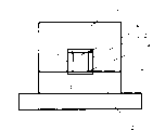
Fig. 1 is the synoptic diagram of polymerization waveguide, and cushion is positioned on the substrate, and core is located immediately on the cushion and goes up clad and is positioned on core upper surface, core sidewall and the cushion.The side interface zone is between the sidewall and last clad of core, and upward interface zone is above core and between the clad, and following interface zone is below core and between the cushion;
Fig. 2 is the synoptic diagram with waveguide of desirable step index structure;
Fig. 3 is for having the synoptic diagram of the waveguide of conventional step index structure in the prior art;
Fig. 4 is the synoptic diagram of the waveguide of being made by photopolymer in the prior art, has following clad and gradient index zone around the core that comprises descending the guiding area in the clad;
Fig. 5 is the synoptic diagram of waveguide of the prior art, has following clad, the guiding area in the following clad, the low-refraction cushion under the gradient index on core side and top and the following clad;
Fig. 6 is the sectional view of waveguide, and this waveguide has the well heater that is connected in clad; With
Fig. 7 is the vertical view that is positioned at the waveguide on the substrate, and wherein waveguide is by the grating marking.
Detailed Description Of The Invention
The invention provides the technique of a kind of monomode optical waveguide and formation fiber waveguide. Waveguide of the present invention comprises substrate 2; Be positioned at substrate 2 lip-deep polymerization cushions 4; Printing opacity single mode polymerization core 8 patterns are located immediately on cushion 4 surfaces; With clad 10 in the polymerization on the sidewall 9 dark-part cushions 4 that are positioned at core 8 upper surfaces and core 8. Key property of the present invention is the refractive index n of core 8cGreater than upper clad refractive index no, upper clad refractive index noAgain greater than the cushion refractive index nb, namely, n whereinb<n
o<n
cAnd Δ n=nc-n
o Common ncWith the cushion refractive index nbDifference be at least about 1.5 times of Δ n.
Referring to Fig. 1, it is the schematic diagram according to waveguide of the present invention. Polymerization cushion 4 initial deposition are on substrate 2 surfaces. Substrate 2 can be any material of wishing to make up waveguide on it, comprises such as silicon silica, GaAs, silicon nitride, glass, quartz, plastics, pottery, the material of crystalline material etc. Substrate 2 can comprise also can not contain other device, for example, and such as the resemblance of groove or circuit or electro-optical device such as laser diode.
Because substrate 2 of the present invention can absorb at important telecommunications optical wavelength place, any part that arrives the propagates light of substrate 2 is all absorbed. 2 pairs of Optical Absorptions of substrate cause the relevant loss of undesirable and polarization of the luminous energy of transmitting signal. The purpose of intermediate buffering layer 4 is that restriction light penetrates into substrate 2 and prevents that any a large amount of light from arriving substrate 2. In order to make cushion by the work of hope ground, be necessary to make its refractive index significantly to be lower than the refractive index of core 8. Polymerization cushion 4 can apply by the known a large amount of distinct methods of prior art, such as spin coating, dip-coating, slot coated, roller coat, blade coating, liquid cast etc. Cushion 4 can comprise the light polyacetylene compound, such as acrylate compounds. Useful acrylate compounds is described below. In case the photopolymerization material layer is deposited on substrate 2 surfaces, is exposed to actinic radiation by integral body and makes its at least part of polymerization. Usually the thickness about 3 of cushion 4 is to about 500 microns. About 5 to about 100 microns thickness be that be fit to and preferred about 10 to about 30 microns.
In order to promote with the adhesion strength between the after-applied polymer layer and control the gradually changing of refractive index at the interface in some cases, the layer that applies at first, comprise described cushion 4, can on purpose basically owe to solidify to improve monomer intert and each layer between the formation of covalent bond.
Cushion 4 deposition and partially polymerized after, core 8 is formed on cushion 4 surfaces. In a kind of embodiment, core 8 is by being deposited on the photosensitive sandwich layer of the single mode of printing opacity upper formation the in cushion 4 surfaces. The methods such as sandwich layer photopolymerizable composition use known technology such as spin coating, dip-coating, slot coated, roller coat, blade coating, liquid cast deposit. Then photosensitive sandwich layer is exposed under the actinic radiation and video picture by the imaging mode, thereby removes the not imaging region of sandwich layer and do not remove the imaging region of sandwich layer. This process is more detailed description below. After this layer video picture, core 8 patterned, printing opacity forms at cushion 4, and partial buffer layer 4 is by partial display. Structure at the core 8 of this fabrication stage is described as fin usually.
In another embodiment of the invention, sandwich layer 8 is by being deposited on pattern printing opacity, the polymerization core material upper formation the in cushion 4 surfaces. The core pattern can use known pattern deposition adding technique or other elimination technique such as reactivity-ion-etching and produce. In another embodiment, the transversal face width of core 8 approximates its cross section height. Usually the transversal face width of sandwich layer 8 and Gao Ge at about 2 μ m to about 10 mu m ranges, more suitably the transversal face width of core and Gao Ge at about 5.5 μ m to about 8 mu m ranges. Usually the width of core 8 is not more than the high twice of about core, and height is not more than wide about twice. In addition, usually core 8 each widely is single mode with height and has identical approximately height and width at it. Usually waveguide dimensions comprises the core of height and width that can be mutually the same, and all is about 2 μ m, about 4 μ m, about 5 μ m, about 6 μ m, about 7 μ m, about 8 μ m, about 9 μ m or about 10 μ m. Usually the wide high about twice of core that also is not more than of core, and the high wide about twice of core that also is not more than. For being minimized to, coupling loss meets the standard single mode glass fibre, the SMF-28 that for example sells for Coming Incorporated, and the core cross sectional dimensions can use between 6 * 6 microns and 8 * 8 microns. Preferably select the transversal face width of core and cross section high with Δ n value, so that waveguide is to greater than about 1300nm, all optical communication wavelength that it is desirable to greater than about 1520nm are single mode. The material of sandwich layer 8 comprises the polymerizable acrylate material, and it is discussed in more detail below.
After core 8 forms, with upper clad 10 be deposited on core 8 upper surfaces, on the sidewall 9 of core 8 and the appearing on the part of cushion 4. The upper clad 10 of photopolymerization also can apply by above-mentioned technology, and then integral body is exposed to actinic radiation. Upper clad 10 can be can will apply light remain in any material in the core 8, can comprise the polymerizable acrylic ester compounds, it is discussed in more detail below. Upper clad 10 common thickness measure above core 8 and are about 3 to about 30 microns in a kind of embodiment, are more typically about 5 to about 20 microns, are more suitable for being about 8 to about 15 microns.
Use the photopolymerization optical material to comprise that the mixture of monomer component and oligomeric component forms waveguide, described component is mixed so that every layer of desirable refractive index to be provided. Every layer of specific refractive index has significant impact to the waveguide effect. When selecting photopolymerization compounds to be used for each core 8, cushion 4 and upper clad 10, the refractive index n of core 8 importantlycGreater than upper clad refractive index no, and Δ n=nc-n
o, and n whereincWith the cushion refractive index nbDifference is at least about 1.5 times of Δ n. More generally, ncAnd nbDifference is at least about 2 times of Δ n. Optimally be ncAnd nbDifference is at least about 3 times of Δ n. In one embodiment of the invention, Δ n changes in about 0.0031 to about 0.079.
In the common application of the present invention, the waveguiding structure of generation is single mode. Guarantee that waveguide is that certain relation between actual cross sections size and waveguide shapes and the Δ n is kept in the single mode requirement. If usually waveguide dimensions is fixed, and if waveguide be single mode, the maximum cutoff of the Δ n that can not surpass is then arranged. Similarly, if Δ n value is fixing, and if waveguide be single mode, the cross-sectional dimension of the waveguide that can not surpass is then arranged. In order to illustrating, following table provided the size of the common waveguide with square cross section and the Δ n maximum that allows between relation. At last, in order to make waveguide-coupled efficient maximum and to make loss of light propagation minimum in the knee, hope is used Δ n value to approximate greatly but is no more than cutoff usually.
Table
| Waveguide core size (μ m) | The Δ n cut-out value of wavelength=1.55 |
| 2×2 | 0.079 |
| 4×4 | 0.019 |
| 6×6 | 0.0086 |
| 7×7 | 0.0064 |
| 8×8 | 0.0049 |
| 10×10 | 0.0031 |
Usually, core 8 refractive index ns
cAbout 1.33 to about 1.7 scopes, or more generally about 1.4 to about 1.55.Usually go up the refractive index n of clad
oAbout 1.3 to about 1.65 scopes, or more generally about 1.35 to about 1.55.Also it is important to select compound to produce refractive index n
bCushion 4 less than the refractive index of core material and last clad.Usually the refractive index of cushion 4 is about 1.3 to about 1.55 scopes, or is more suitable for about 1.3 to about 1.4.These refractive indexes record at the 1550nm place.
In the photoetching of these potpourris, the migration of the monomer component of core 8 enters cushion 4 usually, forms between the bottom 11 of core 8 and the bottom interface zone 14 between the cushion 4, and the refractive index of bottom interface zone 14 is n
f, and between the sidewall 9 of core 8 and the side interface zone 12 between the last clad 10, the refractive index of side interface zone 12 is n
sThese interface zones 12 and 14 can be referring to Fig. 1.Interface zone 12 and 14 has gradient index rather than step index.Interface zone 12 and 14 form be because core 8, the monomer of going up clad 10 and cushion 4 can diffuse out they separately the zone and mix at boundary.As the result who is exposed to actinic radiation subsequently, because core and go up clad then and be cured, these Mixed Zones become permanent fixation.Core 8, the degree that goes up clad 10 and cushion 4 monomer phase counterdiffusion depend on cushion 4, go up the coefficient of diffusion of state of cure, temperature and the used monomer of clad 10 and core 8, and all waveguiding structures are hard in final step solidify before duration of contact between the uncured or partly solidified layer.Monomer be diffused in core 8 bottoms and side maximum mutually few because generally solidify in intermediate fabrication steps in these zones.The generation of low degree of cure be under core-buffer interface situation owing to wish to improve bonding between core 8 and the cushion 4, with under the situation of core side owing to reduce edge's curing dose, this minimizing is because based on the diffraction effect of the lithography of mask or the variation that laser directly is written into the beam intensity of technology.
As shown in Figure 2, shown perfect waveguide with ideal effect.Ideally, light will the centreless diffusion of components enters in the clad ideally 18 that centers on and substrate 2 is gone in zero light absorption by desirable core 16 by transmission.But in fact, traditional prior art waveguide seems more shown in the image pattern 3, because the height of core 22 is wherein gone up clad 24 and had protuberance.This protuberance is undesirable and is disadvantageous.Fig. 4-5 has also shown unfavorable waveguide of the prior art.Fig. 4 shows the waveguide with the guiding area with high index of refraction 32 that forms on following clad 28.Guiding area 32 passes through clad extension arrival substrate 2 down, and wherein a large amount of light can leak and be absorbed.Fig. 5 has shown the waveguide that has low-refraction cushion 34 at following clad for 28 times, attempts to prevent that guiding area 32 from arriving substrates.Because direct light is still leaked and entered the zone 32 that is positioned under the core 26, the type waveguide has high coupling loss, because mate improperly between wave guide mode shape and the traditional fibre mould shape.Limited the loss that these guiding areas cause by removing down clad with the cushion that use has refractive index described herein, thereby the present invention the problems of the prior art have been reduced.
Usually, the refractive index n at interface, side 12
sApproximate the refractive index n at bottom interface 14
fIn one embodiment of the invention, n
sBe the calibration refractive index, it is near about n of the part side interface zone of the sidewall 9 of core
cBe reduced to about n at interface zone 12 places, part side of the most approaching last clad 10
oIn another embodiment of the invention, n
fBe the calibration refractive index, it is near about n of the part bottom interface zone 14 of the bottom 11 of core 8
cBe reduced to about n near part bottom interface zone 14 places of cushion 4
bAlso wish the calibration refractive index n
sApproximately identical, promptly approximately be fit to the calibration refractive index n
fThis means the change of refractive of the per unit length that crosses medium and identical initial value and final value.
Each composition that is used to form each cushion 4, last clad 10 and core 8 can comprise photopolymerization compounds and light trigger.Photopolymerization compounds can be monomer, oligomer or polymkeric substance, it is the alefinically unsaturated compounds that (under atmospheric pressure boiling temperature is higher than 30 ℃) addition polymerization, on-gaseous contains at least one terminal ethylenically unsaturated group, and can form heavy polymer by free radical initiation, chain growth addition polymerization.This compound is known in the prior art.They are selected so that the polymerized unit that forms has the above-mentioned refractive index of hope.The definite of the refractive index of the polymeric compositions of special selection is to determine easily for those skilled in the art.
The polyfunctional acrylic ester monomer is fit to.The formula of polyfunctional acrylic ester is as follows:

For core, the m scope can from 1 to about 6; R
2Be H or CH
3, R
1The bonding that mixes organic molecule segment for aliphatic series, aromatics or aliphatic series and aromatics.The R that is fit to
1Be alkylidene, oxyalkylene group (alkylene oxide), oxidation arlydene (arylene oxide), aliphatic polyether or polyester portion, R
2Be preferably H.Be solvent resistance and the photoetching comparative height of guaranteeing film, cross-linked polymer and polyfunctional acrylic ester monomer (m 〉=2) are fit to.Also wish to use polymkeric substance pliable and tough, low glass transformation temperature (Tg) to reduce the scattered light loss of stress induced final waveguide device.The glass transformation temperature of cross-linked polymer known in the state of the art (Tg) depends on the bonding structure between cross-linking density and the crosslinking points.Also known lower crosslink density and pliable and tough bonding need lower Tg.In order to guarantee lower crosslink density, 1≤m≤3, ideal is that the monomer of m=2 and the long bonding segment between two unsaturated functionality of olefinic are favourable.For the present invention, long bonding segment is meant those mean molecule chain lengths at least about 4 carbon atoms or more, and what be fit to is 6 or more.The pliable and tough bonding structure that is fit to comprises that chain length is greater than the alkylidene of about 3 carbon atoms, poly-(oxirane), poly-(epoxypropane), ethoxylation bisphenol-A, polyethers, thioether, aliphatic series and aromatic hydrocarbon, ether, ester and polysiloxane etc.These structures can be chosen wantonly by any side group that does not reduce polymerizable compound light cumulative power at using light wavelength such as telecom wavelengths 1.31 and 1.55 microns places or do not increase excessive loss and replace.The substituting group that is fit to includes but not limited to alkyl, aryl, alkoxy and sulfoxide radicals etc.In order to guarantee the high patience to thermal degradation and variable color, the R of thermally-stabilised molecular structure
1Be fit to.This R
1Segment should not contain the temperature-sensitive part as aromatic polyurethane group and amide group.In order to guarantee low-birefringence, has the R of low stress optical coefficient and optics polarizability
1Binding is favourable.
For last clad, acrylate also as mentioned above, still, the mean molecule chain length between the unsaturated functionality of olefinic can be about 6 carbon atoms or longer, common 8 or longer and to be more suitable for be 12 or longer.The pliable and tough bonding structure that is fit to comprises that chain length is greater than the alkylidene of 6 carbon atoms, poly-(oxirane), poly-(epoxypropane) and ethoxylation bisphenol-A.
In one embodiment of the invention, the material of each cushion 4, sandwich layer 8 and last clad 10 also comprises polymerizable ester and acrylic acid and contains the aromatics of 2 to 30 carbon atoms and the partial ester of aliphatic polyol.Partial ester and polyoxyalkylene glycol ester also are fit to.Its example is ethylene glycol diacrylate, diacrylate diglycol ester, diacrylate triethyleneglycol ester, diacrylate tetraethylene glycol ester, mean molecular weight poly-ethylene glycol diacrylate and the poly-diacrylate propylene glycol ester, diacrylate propylene glycol ester, dipropylene glycol diacrylate, diacrylate (C in 200 to 2000 scopes
2To C
40) alkane diol ester such as hexanediol diacrylate and diacrylate butanediol ester, diacrylate tripropylene glycol ester, trimethylolpropane triacrylate, the ethoxylated trimethylolpropane triacrylate of mean molecular weight in 500 to 1500 scopes, the diacrylate pentaerythritol ester, pentaerythritol triacrylate, the tetraacrylate pentaerythrite, the diacrylate dipentaerythritol ester, the triacrylate dipentaerythritol ester, dipentaerythritoltetraacrylate, five acrylic acid dipentaerythritol ester, six acrylic acid dipentaerythritol acid esters, eight acrylic acid tripentaerythritol esters, three acrylic acid sorbitol esters, tetrapropylene acid sorbitol ester, five acrylic acid sorbitol esters, six acrylic acid sorbitol esters, the oligoesters of acrylate, two and three acrylic acid glyceride, 1,4-cyclohexane diacrylate, mean molecular weight in 100 to 1500 scopes polyethyleneglycol diacrylate and the potpourri of above-claimed cpd.Multifunctional acrylate oligomers includes but not limited to the epoxide of acroleic acid esterification, the polyurethane of acroleic acid esterification and the polyester of acroleic acid esterification.Photopolymerization compounds comprises the acrylic acid aryl ester.The example of this acrylic acid aryl ester monomer is the aryl ester of diacrylate, three acrylic acid and tetrapropylene acid, for example based on two, three and tetraacrylate of benzene, naphthalene, bisphenol-A, biphenylene, methane biphenylene, fluoroform biphenylene, phenoxy group phenylene etc.Acrylic acid aryl ester monomer can be two, three and a tetraacrylate based on the bisphenol-A structure for multifunctional acrylic acid aryl ester and more generally acrylic acid aryl ester monomer.Common acrylic acid aryl ester monomer is oxyalkylated bisphenol-A diacrylate, as ethoxylation bisphenol-A diacrylate, propoxylation bisphenol-A diacrylate and ethoxylation hexafluoro bisphenol-A diacrylate.Selected acrylic acid aryl ester monomer is an ethoxylation bisphenol-A diacrylate.The polymerizable components of wishing is the monomer with structural formula (I):

In a kind of embodiment, for core, n is about 10 or littler, usually about 4 or littler, more be suitable for about 2 or littler.In a kind of embodiment, for clad, n is about 2 or bigger, usually about 4 or bigger, more be suitable for about 10 or bigger.The multipolymer that contains acrylate also usefully well known in the prior art.Clad comprises the polymerizable components with the ethoxylated bisphenol a diacrylate structure shown in the said structure formula (I) in embodiments, 1≤n≤20 wherein, and common 4≤n≤15 are more suitable for 8≤n≤12.
Polymerisable compound can be multifunctional fluoridizing (methyl) acrylate, and especially those are based on following array structure:

Wherein Y is H or D; X is H, D, F, Cl or CH
3, a is from 2 to 4 integer, R=-CH
2-R
f-CH
2-, or
Or
 R
f=-(CF
2)
k-, or-CF
2O[(CF
2CF
2O)
m(CF2O)
n] CF
2-, or-CF (CF
3) O (CF
2)
4O[CF (CF
3) CF
2O]
pCF (CF
3The k of)-wherein, m, n and p are integer
R
f=-(CF
2)
k-, or-CF
2O[(CF
2CF
2O)
m(CF2O)
n] CF
2-, or-CF (CF
3) O (CF
2)
4O[CF (CF
3) CF
2O]
pCF (CF
3The k of)-wherein, m, n and p are integer
The waveguide of these material production is little of 0.17dB/cm in 1550 nanometers propagation losses.The glass transformation temperature of these materials (Tg) can easily be chosen as the operating temperature that is lower than thermo-optical device.These materials of low Tg type have shown to have negligible birefringence by the grating subsidiary, and have the high-temperature derivative value of refractive index, and it allows to make the thermo-optical device that efficiency is arranged, as optical switch and adjustable grating.Useful (methyl) acrylate of fluoridizing comprises as by polyvalent alcohol
 The tetraacrylate F60TA that T makes, it is commercially available, and it reacts according to as follows from the Ausimont of Milan, ITA S.p.A.:

Other polyfunctional acrylic ester comprises the AkzoChemicals B.V of C6DIACRY available from Dutch Amersfoort:
CH
2=CHCO
2CH
2(CF)
4CH
2O
2CCH=CH
2
L-12043 is available from Saint Paul, the 3M company of Minnesota:
CH
2=CHCO
2CH
2CF(CF
3)O(CF
2)
4O[CF(CF
3)CF
2O]
pCF(CF
3)CH
2O
2CCH=CH
2
L-9367 is similarly available from 3M company:
CH
2=CHCO
2CH
2(CF
2CF
2O)
m(CF
2O)
nCF
2CH
2O
2CCH=CH
2
Though each cushion, last clad and core can be made up of the composition of structural similarity, are lower than the core refractive index in order to make each cushion and last clad refractive index, each application must have different Chemical composition thats.For example, the cushion composition can have the Tg character similar to clad, but need not same composition.Selective light polymeric material and processing conditions so that the Tg of polymerization cushion in about 60 ℃ or lower scope, about usually 40 ℃ or lower, more suitable about 25 ℃ or lower.
The photopolymerization compounds that is used for waveguide core that is characterized as of the present invention is made core, and the glass transformation temperature of core after polymerization is about 80 ℃ or lower, is suitably for about 50 ℃ or lower.The photopolymerization compounds that is used for the waveguide clad that is characterized as of the present invention is made clad, and glass transformation temperature is about 60 ℃ or lower after its polymerization, about usually 40 ℃ or lower, more is suitable for about 25 ℃ or lower.Special Tg can be selected to obtain by the feature of polymeric component with to it by those skilled in the art at an easy rate.This depends on following factors such as molecular weight, unsaturated positional number and polymerizable components cross-linking density.The Tg that single polymerization component itself can be necessary, or polymerizable components can be adjusted by polymerisable monomer, oligomer and/or mixture of polymers that mixing has a Tg of hope.Tg also can control with the temperature of carrying out polymerization by changing exposure duration.
Light polyacetylene compound amount in the poly-composition of each whole light is enough carried out photopolymerization when being exposed to enough actinic radiations.The amount of light polyacetylene compound can be in wide variation in the composition, and when the photopolymer of making as the light transmission component of transmittance device, the usual amounts of spendable photopolymerizable composition can be used.The consumption of phtotpolymerizable compound is about about 35 to about 99.9% of composition weight usually.In the weight of whole composition, the amount of normal light polyacetylene compound in total composition is about 80% to about 99.5%, and is more suitable for being about 95 to about 99%.
Each photosensitive component further comprises the light trigger of at least a generation free radical, and it produces free radical in the photodissociation mode.The normal light initiating agent is a kind of addition polymerization initiating agent of the generation free radical that is activated by actinic light, and (20 ℃ to about 80 ℃ according to appointment) do not have the heat activity under nearly room temperature.Any known photopolymerisable light trigger of acrylate that can make all can use.Light trigger includes but not limited to the quinoxaline compounds that prior art is known; Connect the polyketone aldehyde compound, the alpha-carbonyl compound; Acyloin ether; Triarylimidazoles base dipolymer; The aromatics acyloin that α-alkyl replaces; Multinuclear quinones and s-triazine.
The light trigger that is fit to comprises arone such as benzophenone, the benzophenone of acroleic acid esterification, 2-EAQ, phenanthrenequione, 2-tert-butyl group anthraquinone, 1,2-benzo anthraquinone, 2,3-benzo anthraquinone, 2,3-dichlone, benzyl dimethyl ketal and other arone are as benzoin, benzoin ether such as benzoin methylether, benzoin ethyl ether, benzoin isobutyl ether and benzoin phenylate, methylbenzene acyloin, ethylbenzene acyloin and other benzoin.Light trigger comprise 1-hydroxy-cyclohexyl benzophenone (
 184), benzoin, benzoin ethyl ether, benzoin iso-propylether, benzophenone, benzo dimethyl ketal (Irgacure 651), 2, the 2-diethoxy acetophenone, can available from 2-hydroxy-2-methyl-1-phenyl third-1-ketone of the E.Merck of German Darmstadt (
 1173), 1-[4-(2-hydroxyl-oxethyl) phenyl]-2-hydroxy-2-methyl third-1-ketone (
2959), 2-methyl isophthalic acid-[(4-methyl mercapto) phenyl]-2-morpholino third-1-ketone (
1173), 1-[4-(2-hydroxyl-oxethyl) phenyl]-2-hydroxy-2-methyl third-1-ketone (
2959), 2-methyl isophthalic acid-[(4-methyl mercapto) phenyl]-2-morpholino third-1-ketone (
 907), 2-benzyl-2-dimethylamino-1-(4-morpholino phenyl) fourth-1-ketone (
 369), poly-1-[4-(1-methyl ethylene) phenyl]-2-hydroxy-2-methyl third-1-ketone (Esacure KIP), [4-(4-methylbenzene sulfenyl) phenyl] Benzophenone (
 BMS) available from London Great Lake Fine Chemicals Limited and two camphorquinones.Optimal light trigger is the material that those can flavescence under radiation.This light trigger comprise the benzo dimethyl ketal (
 651), 2-hydroxy-2-methyl-1-phenyl third-1-ketone (
 1173), 1-hydroxyl-cyclohexyl-benzophenone (
 184) and 1-[4-(2-hydroxyl-oxethyl) phenyl]-2-hydroxy-2-methyl third-1-ketone (Darocur2959).
 -T and C6DIACRYL can be fully miscible so that traditional light trigger can be used for ultra-violet curing.For the higher polyfunctional acrylic ester of the rate of fluoridizing, L-12043 and L-9367 material as available from 3M can use fluorinated photoinitiator.
In each photopolymerisable compositions, the amount that produces the light trigger of free radical enough makes photopolymerization compounds be exposed to the photopolymerization of carrying out under enough actinic radiations.In the general assembly (TW) of composition, the common amount of light trigger is about 0.01% to about 10%, or more generally about 0.1% to about 6%, is more suitable for about 0.5% to about 4%.
According to the purpose and the final use of photosensitive composition, other adjuvant also can join in the photosensitive composition.These examples comprise (especially in nanometer range, just particle size is less than about 100nm), dyestuff, free radical scavenger, contrast-enhancing agents, nitrone and ultraviolet absorbers such as solvent, antioxidant, light stabilizer, volumetric expansion agent, filler such as silicon dioxide, titania, glass bead.Compound that antioxidant comprises such as phenols, especially Hinered phenols comprise available from the Ciba-Geigy Corporation's of New York Tarrytown
 1010; Sulfide; Organoboron compound; Organic phosphorus compound; With trade name
1098 N available from Ciba-Geigy, N '-hexa-methylene two (3,5-di-t-butyl-4-hydroxyl hydrocinnamamide).Light stabilizer, the hindered amine as light stabilizer of saying so more specifically include, but are not limited to gather [(6-morpholino-s-triazine-2,4-two bases) [(2,2,6,6-tetramethyl-4-piperidyl) imino group]-hexa-methylene [(2,2,6,6 ,-tetramethyl-4-piperidyl) imino group]], with trade name "
UV-3346 " available from Wilmington, the Cytec Industries of Delaware.The volumetric expansion compound comprises that material is as being called the spiral fashion monomer of Bailey monomer.The example of dyestuff comprises methylene green and methylenum careuleum etc.The free radical scavenger that is fit to comprises oxygen, hindered amine as light stabilizer, hindered phenol, 2,2,6,6-tetramethyl-1-piperidines oxygen base free radical (TEMPO) etc.Suitable contrast-enhancing agents comprises other free radical scavenger such as nitrone.Ultraviolet absorber comprises benzotriazole, hydroxy benzophenone etc.In the general assembly (TW) of composition, these additive capacities are about 0% to about 6%, common about 0.1% to about 1%.The all components of entire combination thing mixes mutually, and optimum is uniform basically potpourri.
1010; Sulfide; Organoboron compound; Organic phosphorus compound; With trade name
1098 N available from Ciba-Geigy, N '-hexa-methylene two (3,5-di-t-butyl-4-hydroxyl hydrocinnamamide).Light stabilizer, the hindered amine as light stabilizer of saying so more specifically include, but are not limited to gather [(6-morpholino-s-triazine-2,4-two bases) [(2,2,6,6-tetramethyl-4-piperidyl) imino group]-hexa-methylene [(2,2,6,6 ,-tetramethyl-4-piperidyl) imino group]], with trade name "
UV-3346 " available from Wilmington, the Cytec Industries of Delaware.The volumetric expansion compound comprises that material is as being called the spiral fashion monomer of Bailey monomer.The example of dyestuff comprises methylene green and methylenum careuleum etc.The free radical scavenger that is fit to comprises oxygen, hindered amine as light stabilizer, hindered phenol, 2,2,6,6-tetramethyl-1-piperidines oxygen base free radical (TEMPO) etc.Suitable contrast-enhancing agents comprises other free radical scavenger such as nitrone.Ultraviolet absorber comprises benzotriazole, hydroxy benzophenone etc.In the general assembly (TW) of composition, these additive capacities are about 0% to about 6%, common about 0.1% to about 1%.The all components of entire combination thing mixes mutually, and optimum is uniform basically potpourri.
In case form the thin or thick film of core photosensitive composition on cushion 4, actinic radiation directly impinges upon on the film with the delineation sandwich layer.Just, the position of core and size are by the pattern decision of the actinic radiation that acts on core layer surface.Must select so that the poly-composition of light aggregates into desirable pattern radiation pattern, and make other zone of film keep not reacting.Photopolymer of the present invention is traditionally by being exposed to the poly-composition of light under the actinic radiation of required wavelength and intensity, and keeps the duration that needs and prepare.Be defined as at visible, the ultraviolet of spectrum or the light of region of ultra-red at this used " actinic radiation ", and electron beam, ion beam or neutron beam or x-ray radiation.Actinic radiation can be the form of irrelevant or coherent light, for example from the light of laser.Photochemical light source, step of exposure, time, wavelength and intensity can in very large range change according to the degree of polymerization of hope, the refractive index and the known other factors of those of ordinary skills of photopolymer.The poly-method of this traditional light and its operating parameter are known in the art.
Actinic radiation sources and radiation wavelength can be in wide variation, and any traditional wavelength and light source all can use.In a kind of embodiment, under short wavelength (or high energy) radiation, carry out photochemical excitation so that the radiation (as chamber light) that often runs into before the operation can not shift to an earlier date the polymerization polymerizable material.Therefore, being exposed to ultraviolet light (300-400nm wavelength) is easily.And deep UV (ultraviolet light) (190-300nm wavelength) exposure also is useful.Light source is high-pressure mercury-xenon arc lamp easily, and the operative wavelength of suitable light filter to select to wish is installed.And short wavelength's coherent radiation is useful to implementing the present invention.Near the UV type argon laser of the some wavelength place work 350nm is wished.And near the frequency multiplication Argon ion laser of exporting the 257nm wavelength is wished very much.Perhaps, also can adopt the multiphoton process that cause by photochemical radiation source of high strength such as laser instrument.Also can not use light trigger and solidify above-mentioned fluorinated monomer by the use electronic beam curing.Can use electron beam or ion beam to excite.Time shutter is usually by several seconds to about 10 minutes.About 10 ℃ to about 60 ℃ usually of temperature, still, room temperature is more suitable for.In addition, these materials can carry out heat curing by using superoxide or other thermal initiator.
The space distribution of control actinic radiation just can drop on the photopolymerization material layer it by classic method.For example, in a kind of classic method, the mask that will have the core pattern of hope is placed between actinic radiation sources and the photopolymerizable composition film.Mask has transparent and zone of opacity, thereby makes radiation only drop on the film surf zone of wishing irradiation.The mask exposure of film is well known in the art, can comprise the core pattern is printed onto the contact on the film, approaching and shadow casting technique.Another kind of traditional spatial control method is used and is comprised such as the guiding of laser beam or electron beam or the actinic radiation sources of focused beam.This radiation beam only intersects with the film surface of fraction photopolymerization material.The core pattern of wishing by at spacescan light beam or mobile substrate so that the point of crossing changes with the little point of crossing around the moving film surface with respect to fixed beam obtains.These use the type of exposure of light beam source is the known direct graphic of state of the art.The accurate shape of cross section of waveguide core and be subjected to directly writing the influence of the light source calibration degree of autofrettage and mask exposure manufacture method in the width in the graded index zone that the core wall forms and degree.Result as required, levels of collimation can change on a large scale.Usually be fit to use high relatively calibration source to determine the waveguide core structure.Calibrating to angle is suitable for less than 10 degree.
The photopolymerizable composition polymerization of sandwich layer forms after the sandwich layer predetermined pattern, and this pattern carries out video picture to remove not imaging area and to stay predetermined pattern.Any traditional developing method all can use, as using the non-irradiated composition of solvent washing.This solvent comprises polar solvent, as pure and mild ketone.Useful solvent is acetone, methyl alcohol, propyl alcohol, tetrahydrofuran and ethyl acetate, and be used for the commodity that the fluoro-ether solvent of high fluorinated monomer such as Ausimont sell by name "
 " those be fit to.
Cushion and clad needn't full solidification, only need partially polymerized.Partially polymerized some acrylate groups that mean still exist after polymerization, promptly are not that all acrylate is converted into stable hydrocarbon.This means acrylate group number greater than 0%, usually greater than about 10%, the most suitable greater than about 25% acrylate group unreacted still.The upper limit of unreacted group number depends on the jellying point of monomer, and it further depends on functionality (the acrylate group number of every monomer).If functionality equals integer f, the unreacted group upper limit should enough cause gelation and obtain by relational expression (1-1/f) * 100% is approximate so.As an example, the remaining unreacted group of tetraacrylate monomer number should be less than 75%, and the remaining unreacted group of diacrylate monomer number is less than 50%.Carry out the partially polymerized of each layer earlier, apply next successive layers then, each layer mixed at the interface mutually at it.The adhesion of this mixing promoting layer can be used for controlling gradually changed refractive index grade at the interface in some cases.
After applying each layer and each layer randomly being carried out patterning or mint-mark with surface or volume diffraction grating, acrylate to any polymerization not yet solidifies firmly, this by blanket formula or burn-out in actinic radiation so that they basically all polymerizations carry out.Diffraction grating 13 is shown in Figure 7.The curing dose of final curing step (per unit square surperficial integrated radiant emittance) typically is about 10 to about 500 times of partly solidified every layer of institute's consumption of using in the aforementioned steps of manufacture.Optimal final curing dosage is about 100 times of middle dosage.In this mode, each layer is in mixing at the interface in the early stage manufacturing step, and ratio that can any hope mixes carrying out the fine setting of each layer and single unit system refractive index, and can guarantee that covalent bond good between each layer adheres.Final structure of wishing is determined that by the final curing step making does not have the further change of structure again.In order to make planar polymerized optical waveguide, need control the refractive index of each core and clad well.This can obtain with the refractive index that obtains to wish by the structure of adjusting the used monomer of each specific coat.In fact, be easy to the required refractive index of can miscible monomer mixing to obtain wishing with some different refractivities.When needs strong reflection grating, also be suitable for the core neutralization and randomly in clad, use more than a kind of monomer.
Except using existing lithography to make the slab guide, also can be by reactive ion etching, littlely duplicate, directly laser inscription or laser ablation are made waveguide core.
The pliability of material makes can make the device with desirable physical strength.Even also can avoid under the very high or low-down temperature breaking when this device is exposed to.Because the good clinging power of material can be made firm device on various substrates, even also can delamination under as high temperature and high humility under some rugged environments.The compatibility that device manufacturing technology and semi-conductor industry are produced is developed the mixed electrical optical circuit.
Waveguide of the present invention can have various suitable cross-sectional shape, as annular, polygon, square, rectangle, trapezoidal and circular be para-curve or Gaussian curve as top and side, the bottom surface is the plane, the place contacts with cushion in the bottom surface.A useful especially aspect of the present invention is to be applied to thermo-optical device.These devices are according to such fact work, and promptly the refractive index of most of material is the function of temperature.Refractive index polymer is a negative value with variation of temperature (dn/dT), and should be worth very big for most of inorganic material.The device of specific design comprises based on the optical switch of grating and tunable filter.Usually on the upper surface of polymer stack, use well heater in the reality, promptly on the last clad or above.The device typical case is implemented in by on material that has high thermal conductivity with respect to polymkeric substance such as the substrate that silicon wafer is formed.Well heater is applied energy to set up thermal gradient, and then its middle and upper part polymeric layer is than following polymeric layer temperature height.Well heater 11 is shown in Figure 6, and it is connected in clad.Because dn/dT is a negative value, polymer stack top refractive index ratio bottom refractive index is low.Refractive index gradient is tending towards making light to be transmitted to substrate downwards along the waveguide that is exposed to this gradient.In the device as switch and adjustable grating, this downward light displacement is undesirable.Under the switch situation, the displacement of hope is horizontal, and not wishing under the grating situation has the light displacement.Waveguiding structure of the present invention is used to limit light (mould) and moves down.This is to finish by such fact, even the low-refraction cushion approaches waveguide core.Influence (the prerequisite n of cushion
c-n
b>1.5* Δ n) can overcome the trend that mould reaches substrate downwards.The improved waveguide geometry configuration of the present invention causes relying on than low-loss and lower polarization of device such as switch and tunable wave length grating.
Following limiting examples is in order to set forth the present invention.
Embodiment 1
Silicon wafer is cleaned, make that with silane treatment the acrylate preparation is had cohesive then.Wafer after the processing is with containing one deck padded coaming spin coating that 75: 25 weight % fluoridize diacrylate/fluoridize tetraacrylate and contain the potpourri of light trigger.Then cushion integral body is exposed to actinic radiation so that it is partly solidified.Then cushion is carried out spin coating with containing the core material of fluoridizing tetraacrylate/fluoroalkyl acrylate and being mixed with light trigger that 92: 8 weight % have 8 fluorine atoms.This material is selected so that its refractive index is higher than the cushion refractive index.Core layer thickness depends on the duct height of hope, typically for single mode waveguide in the 5-9 micrometer range.Then with core material by mask exposure in ultraviolet light.The core exposure dose is adjusted the sticky limit of the clad that centers on of and hope wide with the core that obtains to wish.Unexposed material is developed with solvent then.Then with comprising that the last coating layer material of fluoridizing tetraacrylate and being mixed with light trigger carries out spin coating to core.Solidify with final dose then and go up clad, this final dose penetrates all layers and finishes the curing of the upper and lower.
To contain 25 weight % (wt%) fluoridizes the potpourri that tetraacrylate F60TA, 75wt% fluoridize diacrylate L-9367 and mixes with the 2wt% fluorinated photoinitiator to form homogeneous solution.Then this solution is spun on the silicon substrate, and under high-pressure mercury-xenon lamp with about 15mW/cm
2Irradiance solidify to form the thick cushion of 10 μ m.The refractive index of cushion is 1.313.To contain 92wt% and fluoridize core potpourri and the 1wt% light trigger that tetraacrylate F60TA, 7wt% fluoridize diacrylate " C6DIACRY "
 1173 mix to form homogeneous solution.Then this core solution is applied on the cushion.With its by photomask exposure in mercury-xenon lamp and develop to form refractive index be 1.336 the thick core of 6 μ m.99wt% be will contain and tetraacrylate F60TA and 1wt% light trigger fluoridized
 1173 last clad composition mixes the formation homogeneous solution.Then this solution is spun on the core and solidify under the mercury lamp with form the thick refractive index of 12 μ m be 1.329 on clad.
Although the present invention is demonstrated especially, and be described with the embodiment that is fit to, those of ordinary skills are easy to without departing from the spirit and scope of the present invention changes and improvements are being carried out in invention.Claim should be interpreted as being intended to cover alternative and all equivalents of disclosed embodiment, above-mentioned discussion.
Claims (25)
1. monomode optical waveguide that is formed on the substrate, this substrate is determined the surface, this monomode optical waveguide comprises:
Be positioned at the polymerization cushion on the substrate surface, this polymerization cushion determines that surface and refractive index are n
b
Be located immediately at the patterned printing opacity sandwich layer on the buffer-layer surface, this patterned printing opacity sandwich layer is determined upper surface and pair of sidewalls, and the refractive index of this patterned printing opacity sandwich layer is n
c
Be positioned at the pair of sidewalls of core upper surface, core and the last clad on the cushion, refractive index of clad is n on this
o, make n
b<n
o<n
cAnd Δ n=n
c-n
o, wherein Δ n value produces single mode waveguide in optical communication wavelength place;
Side interface zone between in the pair of sidewalls of patterned printing opacity sandwich layer each and the last clad, the refractive index of this side interface zone are n
sWith
Between the bottom of patterned printing opacity sandwich layer and the bottom interface zone between the polymerization cushion, the refractive index of this bottom interface zone is n
f
2. the monomode optical waveguide of claim 1, its SMIS have transversal face width and xsect height, and wherein transversal face width and xsect height select with Δ n value, so that waveguide is single mode for all optical communications wavelength greater than about 1300nm.
3. the monomode optical waveguide of claim 1, its SMIS have transversal face width and xsect height, and wherein transversal face width and xsect height select with Δ n value, so that waveguide is single mode for all optical communications wavelength greater than about 1520nm.
4. the monomode optical waveguide of claim 1, the refraction n of wherein patterned printing opacity sandwich layer
cRefractive index n with the polymerization cushion
bDifference be at least about 1.5 times of Δ n.
5. the monomode optical waveguide of claim 1, wherein n
cWith n
bDifference be at least about 2 times of Δ n.
6. the monomode optical waveguide of claim 1, wherein n
cWith n
bDifference be at least about 3 times of Δ n.
7. the monomode optical waveguide of claim 1, wherein the thickness of polymerization cushion is at least about 3 microns.
8. the monomode optical waveguide of claim 1, wherein Δ n is about 0.0031 to about 0.079.
9. the monomode optical waveguide of claim 1, wherein patterned printing opacity sandwich layer has transversal face width and xsect height, and its about 2 μ m that respectively do for oneself are to about 10 μ m.
10. the monomode optical waveguide of claim 1, wherein patterned printing opacity sandwich layer has transversal face width and xsect height, and its about 2 μ m that respectively do for oneself are to about 10 μ m, and wherein transversal face width is not more than high about twice, and height is not more than about twice of transversal face width.
11. the monomode optical waveguide of claim 1, wherein patterned printing opacity sandwich layer has transversal face width and xsect height, and it is about 6 μ m separately to about 8 μ m.
12. the monomode optical waveguide of claim 1, wherein patterned printing opacity sandwich layer has transversal face width and xsect height, transversal face width approximates the xsect height, and wherein transversal face width and xsect height are selected from the size of about 2 μ m, about 4 μ m, about 5 μ m, about 6 μ m, about 7 μ m, about 8 μ m and about 10 μ m separately.
13. the monomode optical waveguide of claim 1, wherein patterned printing opacity sandwich layer has height and width, and patterned printing opacity sandwich layer is wide and high to being single mode at each.
14. the monomode optical waveguide of claim 1, wherein n
sApproximate n
f
15. the monomode optical waveguide of claim 1, wherein n
sAbout n of the part side interface zone of the adjacent wall from the pair of sidewalls of the most approaching patterned printing opacity sandwich layer
cBe reduced to the most about n at the interface zone place, part side of approaching last clad
o
16. the monomode optical waveguide of claim 1, wherein n
fAbout n at the part bottom interface zone place of the bottom of the most approaching patterned printing opacity sandwich layer
cBe reduced to about n near the part bottom interface zone place of polymerization cushion
u
17. the monomode optical waveguide of claim 1, wherein n
sAbout n of the part side interface zone of the adjacent wall from the pair of sidewalls of the most approaching patterned printing opacity sandwich layer
cBe reduced to the most about n at the interface zone place, part side of approaching last clad
oAnd
n
fAbout n from the part bottom interface zone of the bottom of the most approaching patterned printing opacity sandwich layer
cBe reduced to about n near the part bottom interface zone place of polymerization cushion
u
18. the monomode optical waveguide of claim 17, wherein calibration refractive index n
sApproximately and the calibration refractive index n
fBe complementary.
19. a low-light electrical part comprises:
The waveguide of claim 1; And
Be positioned at the well heater on the clad upper surface.
20. a low-light electrical part comprises:
The waveguide of claim 1; And
Polymerization cushion, patterned printing opacity sandwich layer or on form the surface undulation or the Volume Grating of pattern in the clad at least in one deck.
21. a method that forms monomode optical waveguide on substrate, this substrate is determined the surface, and this method comprises the steps:
Deposition polymerization cushion on substrate surface, this polymerization cushion determine that surface and refractive index are n
b
On the polymerization buffer-layer surface, directly deposit patterned printing opacity sandwich layer and be not with any middle layer, the core that described patterned printing opacity sandwich layer determines to have upper surface and pair of sidewalls, the refractive index of this patterned printing opacity sandwich layer is n
cWith
On patterned printing opacity sandwich layer upper surface, deposit clad on the sidewall of patterned printing opacity sandwich layer and on a part of polymerization cushion, refractive index of clad is n on this
o, make n
b<n
o<n
cAnd Δ n=n
c-n
o
Moving to the small part light transmissive material of its center core layer enters cushion, thereby forms between the bottom of core and the bottom interface zone between the cushion, and the refractive index of this bottom interface zone is n
f, and form between the sidewall of core and the side interface zone between the last clad, the refractive index of this side interface zone is n
s
22. a method that forms monomode optical waveguide on substrate, described substrate is determined the surface, and this method comprises the steps:
Deposit cushion on substrate surface, this cushion is n by refractive index
bThe polymeric material manufacturing, described cushion is determined the surface;
Directly deposit sandwich layer and be not with any middle layer on buffer-layer surface, this sandwich layer is n by refractive index
cThe light transmissive material manufacturing;
Make sandwich layer become pattern to determine to have the core and the expose portion cushion of upper surface and pair of sidewalls; And
Deposit clad on the expose portion of the sidewall of sandwich layer upper surface, sandwich layer and cushion, refractive index of clad is n on this
o, make n
b<n
o<n
cAnd Δ n=n
c-n
o, wherein Δ n value produces single mode waveguide in the optical communications wavelength place;
Moving to the small part light transmissive material of its center core layer enters cushion, thereby forms between the bottom of core and the bottom interface zone between the cushion, and the refractive index of this bottom interface zone is n
f, and form between the sidewall of core and the side interface zone between the last clad, the refractive index of this side interface zone is n
s
23. a method that forms optical waveguide on substrate, described substrate is determined the surface, and this method comprises the steps:
In substrate surface deposition polymerization cushion, this polymerization cushion determines that surface and refractive index are n
b
Directly deposit photosensitive sandwich layer and be not with any middle layer on the polymerization buffer-layer surface, this photosensitive sandwich layer is determined upper surface, and photosensitive sandwich layer refractive index is n
c
By the imaging mode printing opacity sandwich layer is exposed to actinic radiation;
The photosensitive sandwich layer of video picture is not removed the imaging region of photosensitive sandwich layer with the not imaging region of removing photosensitive sandwich layer, thereby forms patterned printing opacity waveguide core, and it has a pair of sidewall that is positioned on the polymerization cushion, and part appears the exposed portion of polymerization cushion; And
On patterned printing opacity waveguide core upper surface, deposit clad on the described pair of sidewalls of patterned printing opacity waveguide core and on the exposed portion of polymerization cushion, refractive index of clad is n on this
o, make n
b<n
o<n
cAnd Δ n=n
c-n
o
24. a monomode optical waveguide that is formed on the substrate, this substrate is determined the surface, and this monomode optical waveguide comprises:
Be positioned at the polymerization cushion on the substrate surface, this polymerization cushion determines that surface and refractive index are n
b
Be located immediately at the patterned printing opacity polymerization sandwich layer on the buffer-layer surface, this patterned printing opacity sandwich layer is determined upper surface and pair of sidewalls, and the refractive index of this patterned printing opacity sandwich layer is n
c
Be positioned at clad in the pair of sidewalls of core upper surface, core and the polymerization on the cushion, refractive index of clad is n on this
o, make n
b<n
o<n
cAnd Δ n=n
c-n
o, wherein Δ n value produces single mode waveguide in optical communication wavelength place; With
In patterned printing opacity polymerization sandwich layer and polymerization, form the Volume Grating of pattern in the clad.
25. the monomode optical waveguide of claim 24, it also is included in the Volume Grating that forms pattern in the polymerization cushion.
Applications Claiming Priority (2)
| Application Number | Priority Date | Filing Date | Title |
|---|---|---|---|
| US09/846,691 US6542684B2 (en) | 2001-05-01 | 2001-05-01 | Optimized multi-layer optical waveguiding system |
| US09/846,691 | 2001-05-01 |
Publications (2)
| Publication Number | Publication Date |
|---|---|
| CN1549937A CN1549937A (en) | 2004-11-24 |
| CN100406935C true CN100406935C (en) | 2008-07-30 |
Family
ID=25298660
Family Applications (1)
| Application Number | Title | Priority Date | Filing Date |
|---|---|---|---|
| CN028091973A Expired - Fee Related CN100406935C (en) | 2001-05-01 | 2002-04-04 | Optimized multi-layer optical waveguiding system |
Country Status (6)
| Country | Link |
|---|---|
| US (1) | US6542684B2 (en) |
| EP (1) | EP1393101A4 (en) |
| JP (1) | JP4138494B2 (en) |
| KR (1) | KR100832678B1 (en) |
| CN (1) | CN100406935C (en) |
| WO (1) | WO2002088795A1 (en) |
Families Citing this family (26)
| Publication number | Priority date | Publication date | Assignee | Title |
|---|---|---|---|---|
| US7078445B2 (en) * | 2001-02-01 | 2006-07-18 | E. I. Du Pont De Nemours And Company | Photosensitive acrylate composition and waveguide device |
| JP4066670B2 (en) * | 2002-02-19 | 2008-03-26 | オムロン株式会社 | Light switch |
| US6904219B1 (en) * | 2002-07-26 | 2005-06-07 | Boston Laser, Inc. | Ultra high-power continuous wave planar waveguide amplifiers and lasers |
| KR20040021710A (en) * | 2002-08-29 | 2004-03-11 | 주식회사 코오롱 | A plastic optical fiber with excellent thermo oxidative stabilization, and a process of preparing the same |
| JP3890046B2 (en) * | 2002-10-07 | 2007-03-07 | 日本電信電話株式会社 | Method for manufacturing planar circuit type optical element |
| US7776236B2 (en) * | 2003-07-25 | 2010-08-17 | General Electric Company | Index contrast enhanced optical waveguides and fabrication methods |
| JP2005157090A (en) * | 2003-11-27 | 2005-06-16 | Mitsumi Electric Co Ltd | Optical waveguide device |
| TWI285664B (en) * | 2003-12-25 | 2007-08-21 | Kansai Paint Co Ltd | Curable resin composition for optical waveguide, curable dry film for optical waveguide, waveguide, and, method for manufacturing optical waveguide |
| JP4318036B2 (en) * | 2004-02-16 | 2009-08-19 | オムロン株式会社 | Optical waveguide |
| JP4894995B2 (en) * | 2004-10-21 | 2012-03-14 | Jsr株式会社 | Photosensitive resin composition for optical waveguide, optical waveguide and method for producing the same |
| US7400809B2 (en) | 2004-12-10 | 2008-07-15 | General Electric Company | Optical waveguide devices and method of making the same |
| BRPI0607463A2 (en) * | 2005-02-15 | 2009-09-08 | Rpo Pty Ltd | photolithographic standardization of polymeric materials |
| US8351752B2 (en) * | 2006-03-06 | 2013-01-08 | Hitachi Chemical Company, Ltd. | Flexible optical waveguide, method for manufacturing such flexible optical waveguide, and optical module |
| US8120595B2 (en) * | 2006-05-01 | 2012-02-21 | Rpo Pty Limited | Waveguide materials for optical touch screens |
| JP2009015214A (en) * | 2007-07-09 | 2009-01-22 | Tokai Univ | Method of manufacturing self-forming optical waveguide |
| JP5580511B2 (en) * | 2007-10-22 | 2014-08-27 | パナソニック株式会社 | Method for manufacturing photoelectric composite substrate |
| EP2103974A1 (en) * | 2008-03-21 | 2009-09-23 | Nitto Denko Corporation | Optical waveguide having grating and method of forming the same |
| JP2011039489A (en) * | 2009-07-17 | 2011-02-24 | Nitto Denko Corp | Method of manufacturing optical waveguide device |
| JP2012073358A (en) * | 2010-09-28 | 2012-04-12 | Nitto Denko Corp | Method for manufacturing optical waveguide for connector |
| US8649645B2 (en) | 2011-06-10 | 2014-02-11 | Xyratex Technology Limited | Optical waveguide and a method of fabricating an optical waveguide |
| CN103560133B (en) * | 2013-10-18 | 2015-09-09 | 绵阳芯联芯通信科技有限公司 | Based on the manufacture method of silica-based light passive integrated devices design platform |
| US11460609B2 (en) | 2018-04-02 | 2022-10-04 | Magic Leap, Inc. | Hybrid polymer waveguide and methods for making the same |
| US11067749B2 (en) * | 2019-11-21 | 2021-07-20 | Globalfoundries U.S. Inc. | Waveguides with cladding layers of gradated refractive index |
| CN114563842A (en) * | 2020-11-27 | 2022-05-31 | 深南电路股份有限公司 | Refractive index gradient polymer waveguide and manufacturing method thereof |
| EP4130824A4 (en) * | 2020-11-27 | 2023-07-12 | Shennan Circuits Co., Ltd. | Graded-index polymer waveguide and manufacturing method therefor |
| CN114895413B (en) * | 2022-03-28 | 2023-12-19 | 深圳技术大学 | Waveguide with pore cladding structure and preparation method thereof |
Citations (6)
| Publication number | Priority date | Publication date | Assignee | Title |
|---|---|---|---|---|
| US5291574A (en) * | 1991-11-27 | 1994-03-01 | France Telecom | Method for manufacturing strip optical waveguides |
| US5837804A (en) * | 1995-07-27 | 1998-11-17 | Hitachi Chemical Company, Ltd. | Polyimides and optical parts obtained by using the same |
| US5896484A (en) * | 1996-02-15 | 1999-04-20 | Corning Incorporated | Method of making a symmetrical optical waveguide |
| US5940568A (en) * | 1996-11-19 | 1999-08-17 | Alcatel Alsthom Compagnie Generale D'electricite | Planar optical waveguide, planar optical waveguide with Bragg grating, and method of fabricating such a planar optical waveguide |
| EP0961139A1 (en) * | 1997-02-19 | 1999-12-01 | Hitachi, Ltd. | Polymer optical waveguide, optical integrated circuit, optical module and optical communication apparatus |
| US6210867B1 (en) * | 1997-02-26 | 2001-04-03 | Samsung Electronics Co., Ltd. | Method for fabricating low-loss optically active device |
Family Cites Families (15)
| Publication number | Priority date | Publication date | Assignee | Title |
|---|---|---|---|---|
| US4609252A (en) | 1979-04-02 | 1986-09-02 | Hughes Aircraft Company | Organic optical waveguide device and method of making |
| JPH01138509A (en) | 1987-11-26 | 1989-05-31 | Asahi Chem Ind Co Ltd | High-density optical waveguide and its manufacture |
| GB2222465A (en) * | 1988-09-03 | 1990-03-07 | Marconi Gec Ltd | Optical waveguide having low light loss |
| FR2658307A1 (en) * | 1990-02-13 | 1991-08-16 | Thomson Csf | INTEGRATED OPTICAL WAVEGUIDE AND METHOD FOR MAKING THE SAME. |
| US5143577A (en) * | 1991-02-08 | 1992-09-01 | Hoechst Celanese Corporation | Smooth-wall polymeric channel and rib waveguides exhibiting low optical loss |
| TW262537B (en) | 1993-07-01 | 1995-11-11 | Allied Signal Inc | |
| TW293090B (en) * | 1995-02-17 | 1996-12-11 | Allied Signal Inc | |
| JPH11508699A (en) | 1995-06-28 | 1999-07-27 | アクゾ ノーベル ナムローゼ フェンノートシャップ | Optical device with at least five layers |
| US5932397A (en) * | 1996-05-28 | 1999-08-03 | Rvm Scientific, Inc. | Multicolor lithography for control of three dimensional refractive index gradient processing |
| JPH1039151A (en) | 1996-07-25 | 1998-02-13 | Hitachi Cable Ltd | Optical waveguide and its production |
| US6335149B1 (en) | 1997-04-08 | 2002-01-01 | Corning Incorporated | High performance acrylate materials for optical interconnects |
| US6157765A (en) * | 1998-11-03 | 2000-12-05 | Lucent Technologies | Planar waveguide optical amplifier |
| US6306563B1 (en) * | 1999-06-21 | 2001-10-23 | Corning Inc. | Optical devices made from radiation curable fluorinated compositions |
| JP2001066445A (en) * | 1999-08-26 | 2001-03-16 | Oki Electric Ind Co Ltd | Optical waveguide and its formation |
| EP1354229A2 (en) * | 2000-07-10 | 2003-10-22 | Massachusetts Institute Of Technology | Graded index waveguide |
-
2001
- 2001-05-01 US US09/846,691 patent/US6542684B2/en not_active Expired - Fee Related
-
2002
- 2002-04-04 WO PCT/US2002/010946 patent/WO2002088795A1/en active Application Filing
- 2002-04-04 EP EP02723793A patent/EP1393101A4/en not_active Withdrawn
- 2002-04-04 CN CN028091973A patent/CN100406935C/en not_active Expired - Fee Related
- 2002-04-04 KR KR1020037014232A patent/KR100832678B1/en not_active IP Right Cessation
- 2002-04-04 JP JP2002586040A patent/JP4138494B2/en not_active Expired - Fee Related
Patent Citations (6)
| Publication number | Priority date | Publication date | Assignee | Title |
|---|---|---|---|---|
| US5291574A (en) * | 1991-11-27 | 1994-03-01 | France Telecom | Method for manufacturing strip optical waveguides |
| US5837804A (en) * | 1995-07-27 | 1998-11-17 | Hitachi Chemical Company, Ltd. | Polyimides and optical parts obtained by using the same |
| US5896484A (en) * | 1996-02-15 | 1999-04-20 | Corning Incorporated | Method of making a symmetrical optical waveguide |
| US5940568A (en) * | 1996-11-19 | 1999-08-17 | Alcatel Alsthom Compagnie Generale D'electricite | Planar optical waveguide, planar optical waveguide with Bragg grating, and method of fabricating such a planar optical waveguide |
| EP0961139A1 (en) * | 1997-02-19 | 1999-12-01 | Hitachi, Ltd. | Polymer optical waveguide, optical integrated circuit, optical module and optical communication apparatus |
| US6210867B1 (en) * | 1997-02-26 | 2001-04-03 | Samsung Electronics Co., Ltd. | Method for fabricating low-loss optically active device |
Also Published As
| Publication number | Publication date |
|---|---|
| EP1393101A1 (en) | 2004-03-03 |
| CN1549937A (en) | 2004-11-24 |
| JP4138494B2 (en) | 2008-08-27 |
| US20030026569A1 (en) | 2003-02-06 |
| KR100832678B1 (en) | 2008-05-27 |
| KR20040015227A (en) | 2004-02-18 |
| JP2004534262A (en) | 2004-11-11 |
| EP1393101A4 (en) | 2006-06-21 |
| US6542684B2 (en) | 2003-04-01 |
| WO2002088795A1 (en) | 2002-11-07 |
Similar Documents
| Publication | Publication Date | Title |
|---|---|---|
| CN100406935C (en) | Optimized multi-layer optical waveguiding system | |
| US6335149B1 (en) | High performance acrylate materials for optical interconnects | |
| US7011932B2 (en) | Polymer waveguide fabrication process | |
| CN1267754C (en) | Design of low insertion loss, single-mode polymeric waveguides | |
| KR100679383B1 (en) | Optical devices made from radiation curable fluorinated compositions | |
| CN100384910C (en) | Optical devices made from radiation curable fluorinated compositions | |
| CN100385277C (en) | Method for apodizing a planar waveguide grating | |
| US20030054092A1 (en) | One step laser fabrication of polymer wave-guided structures having varying width and height, and their application to pigtailing of optical fibers | |
| JP2002277662A (en) | Method for manufacturing optical waveguide coupler |
Legal Events
| Date | Code | Title | Description |
|---|---|---|---|
| C06 | Publication | ||
| PB01 | Publication | ||
| C10 | Entry into substantive examination | ||
| SE01 | Entry into force of request for substantive examination | ||
| C14 | Grant of patent or utility model | ||
| GR01 | Patent grant | ||
| C17 | Cessation of patent right | ||
| CF01 | Termination of patent right due to non-payment of annual fee |
Granted publication date: 20080730 Termination date: 20110404 |