CN100380266C - Bias circuit for maintaining a constant value of transconductance divided by load capacitance - Google Patents
Bias circuit for maintaining a constant value of transconductance divided by load capacitance Download PDFInfo
- Publication number
- CN100380266C CN100380266C CNB028061764A CN02806176A CN100380266C CN 100380266 C CN100380266 C CN 100380266C CN B028061764 A CNB028061764 A CN B028061764A CN 02806176 A CN02806176 A CN 02806176A CN 100380266 C CN100380266 C CN 100380266C
- Authority
- CN
- China
- Prior art keywords
- grid
- capacitor
- nmos
- node
- ground
- Prior art date
- Legal status (The legal status is an assumption and is not a legal conclusion. Google has not performed a legal analysis and makes no representation as to the accuracy of the status listed.)
- Expired - Fee Related
Links
Images


Classifications
-
- G—PHYSICS
- G05—CONTROLLING; REGULATING
- G05F—SYSTEMS FOR REGULATING ELECTRIC OR MAGNETIC VARIABLES
- G05F3/00—Non-retroactive systems for regulating electric variables by using an uncontrolled element, or an uncontrolled combination of elements, such element or such combination having self-regulating properties
- G05F3/02—Regulating voltage or current
- G05F3/08—Regulating voltage or current wherein the variable is dc
- G05F3/10—Regulating voltage or current wherein the variable is dc using uncontrolled devices with non-linear characteristics
- G05F3/16—Regulating voltage or current wherein the variable is dc using uncontrolled devices with non-linear characteristics being semiconductor devices
- G05F3/20—Regulating voltage or current wherein the variable is dc using uncontrolled devices with non-linear characteristics being semiconductor devices using diode- transistor combinations
- G05F3/205—Substrate bias-voltage generators
Abstract
A bias circuit (126) is described for use in biasing an operational amplifier (110) to maintain a constant transconductance divided by load capacitance (i.e. a constant gm/CL) despite temperature and process variations and despite body effects. The bias circuit (126) includes a pair of current source devices and a switched capacitor (SC) equivalent resistor circuit (136) for developing an equivalent resistance between the current source devices. By providing an SC equivalent resistor circuit clocked by non-overlapping fixed clock signals, the gm/CL of the bias circuit is maintained substantially constant. Hence, a fixed bandwidth is maintained within the operation amplifier being biased. When employed in connection with operationa amplifiers of an SC circuit, the constant bandwidth enables the SC circuit to operate at a constant switching speed despite temp and process variation. Furthermore, by positioning the resistance quivalent circuit (136) between the current source devices of the bias circuit, voltage differentials between the sources are eliminated thereby removing any threshold voltage mismatch and thus compensating for body effect variations.
Description
Background of invention
I. invention field
The present invention relates generally to integrated circuit, relate in particular to the operational amplifier or other the CMOS biasing circuit that uses the device of NMOS or PMOS differential pair to setover that are used for switched capacitor (SC).
II. description of Related Art
The operational amplifier that comprises differential pair in integrated circuit usually as being used as the assembly of SC analog signal processing circuit.Some characteristic temperature variation or process variation in order to ensure operational amplifier all roughly keep constant, and biasing circuit is used with the differential pair of operational amplifier.Example is included in interior constant current or the constant transconductance (g of differential pair that is used to keep operational amplifier
m) biasing circuit.Constant g
mMore effective than constant current.For the operational amplifier that uses in the SC circuit, the arithmetic speed of SC circuit mainly is subjected to the restriction of the unity gain bandwidth of operational amplifier.More particularly, be the majorant of operational amplifier unity gain bandwidth the Time Created of SC circuit, and wherein unity gain bandwidth is provided by following formula:
In the formula: g
mBe the mutual conductance of operational amplifier, C
LBe service load electric capacity.
Therefore, improve the speed of performance of SC circuit, do not need only to provide constant g
mBiasing circuit.On the contrary, preferably provide constant g
m/ C
LBiasing circuit.The various conventional biasing circuit that is used for operational amplifier is described below and the unity gain bandwidth problem that produces about biasing circuit has been discussed.
Fig. 1 has illustrated the exemplary operational amplifier 10 that is applicable to SC circuit.Operational amplifier 10 comprise a nmos device differential pair 12 and 14 with a PMOS current mirror device differential pair 13 and 15.As shown in the figure, these four devices are connected positive voltage source V
DDAnd between the node A.The right grid of nmos device links to each other with 18 with a pair of voltage input line 16 respectively.As shown in the figure, output line 20 links to each other with PMOS device 15 with node interconnection nmos device 14.As load capacitance C
LCapacitor 21 output signal is coupled to external loading 22.In order to ensure such as electric current or g
mSome circuit characteristic so no matter temperature or process changes and can both keep constant, operational amplifier is setovered with an offset signal, this offset signal provides along offset line 25, and is applied in the grid of the additional nmos device 24 that is connected between node A and the ground.
The operational amplifier that Fig. 2 has illustrated Fig. 1 with being used to keep Heng Du with the combining of the irrelevant biasing circuit 26 of the variation of temperature variation and process.Biasing circuit 26 comprises the current source 27 that combines with independent nmos device 29, and nmos device 29 is worked as current mirror.Adopt this structure to keep constant current to have nothing to do and be directly proportional with the electric current that provides by current source 27 with the variation of temperature variation and process.
Yet, the g of operational amplifier
mDo not remain constant.And the g of the operational amplifier of Fig. 2
mProvide by following formula:
In the formula, I
0Be bias current, v
GSBe the gate source voltage of device 12, V
TIt is the threshold value of device 12.V
TChange with temperature and process.Therefore, g
mChange along with the fluctuation of temperature and process.In addition, for great majority are used, load capacitance (C
L) also change about ± 10% with the process variation.Therefore, the unity gain bandwidth of the operational amplifier of usefulness constant-current source bias can be because temperature variation and the caused g of process variation
mAnd C
LChange and cause tangible change.Therefore, adopt the speed ability of the SC circuit of operational amplifier to demote.
Fig. 3 has illustrated the operational amplifier 10 of Fig. 1 and is irrelevant and keep constant g with the variation of temperature variation and process
mThe combination of bias current 30.In brief, bias current comprises a pair of nmos device 32 and 34 that is connected between a pair of Node B and C and the ground.PMOS device 33 links to each other with node C with 35 grid.g
mAdjusting resistor 36 is connected between the source electrode and ground of nmos device 34.Resistor 36 generally is positioned at outside the chip, allows to set after chip manufacturing resistance again.In the use, biasing circuit 30 is worked as current mirror, and to produce a bias current, it is the nmos device 12 of operational amplifier and 14 g
mBe set as and g
mThe amount that the resistance of adjustment resistor 36 is inversely proportional to.As known in the art, biasing circuit is actually the MOS pattern of automatic biasing Widlar current source.
Like this, the biasing circuit of Fig. 3 has roughly been guaranteed the g of operational amplifier
mDo not change with process and variation of temperature (single order at least).More particularly, the Kirchoff voltage level of circuit is provided by following formula:
I
0R+v
GS2=v
GS1
The quadratic equation of supposing drain saturation current is:
If the device 32 of supposition biasing circuit and 34 threshold voltage equate (ignoring bulk effect), then:
v
GS1-V
T=2(v
GS2-V
T)
Therefore:
Thereby and,
Like this, do not consider bulk effect, the g of operational amplifier device
mOnly with g
mThe resistance of adjusting resistor 36 is directly proportional.Unfortunately, in actual integrated circuit, bulk effect can form major issue.In brief, the caused threshold voltage V of the voltage difference between bulk effect and source electrode and substrate
TVariation relevant.The square root of voltage is directly proportional between the variation in the voltage threshold and source electrode and substrate.
In the circuit of Fig. 3, the variation in the threshold voltage causes two questions of independence.First problem is that the variation by the source voltage of the nmos device 32 of biasing circuit and 34 is produced.Because the source electrode of nmos device 34 is connecting the different voltages of device 32, so g
mBe not simply to be directly proportional, but provide by following formula with the resistance of resistor 36:
Wherein
This g
mFormula can from following system of equations, derive:
v
gs1=v
gs2+I·R-v
terr
And because
Wherein
So
Obtain
Obtain
At last
The second individual effects problem be owing to the device 32 of biasing circuit and 34 and the device 12 and 14 of operational amplifier between antipode produce.The absolute current that produces in the biasing circuit is directly proportional with threshold voltage, so any variation between the voltage of source all can cause different g
mValue.Owing to fixed the common mode input of operational amplifier, so the source voltage of device 12 and 14 can change the g of generation non tracking with process
mAs a result, the variation of temperature variation and process does not obtain CMOS biasing circuit shown in Figure 1 full remuneration, and this causes operational amplifier g
mVariation.Thereby unity gain bandwidth is affected once more.
U.S. Patent number 6323725, be entitled as in " Constant Transconductance Bias Circuit havingBody Effect Cancellation Circuitry " a kind of improved constant g has been described
mBiasing circuit, it also compensates the variation that is caused by bulk effect, thereby constant g is provided except the variation that causes of compensation by temperature or process
mYet as mentioned above, the speed ability of the SC circuit of associative operation amplifier is subjected to the restriction of operational amplifier unity gain bandwidth.Even constant g is provided
mBiasing circuit, unity gain bandwidth may be still with biasing circuit load capacitance (C
L) variation and change.Thereby, wish very for operational amplifier or adopt the use of other right device of nmos differential that a kind of improved biasing circuit can be provided that the variation and the bulk effect of it and temperature and process all keep constant in fact g
m/ C
L, this is primarily aimed at purpose of the present invention.
Summary of the invention
According to a first aspect of the present invention, change all constant g in order to keep temperature and process
m/ C
L, a kind of biasing circuit that is applicable to the biasing differential pair is provided, for example, the nmos differential that is used for operational amplifier is right.Biasing circuit comprises a pair of current source device and is used to form the equivalent resistance circuit of the equivalent resistance between current source device.The equivalent resistance circuit is included in and connects this sampling capacitor to linking to each other between the sampling node of current source device and the ground.The input of first clock is connected between the sampling node and first current source device, and the second clock input is connected between the sampling node and second current source device.The input of first and second clocks provides non-overlapped clock signal with preset sampling frequency, thereby sets up equivalent resistance.Voltage-setting circuitry links to each other with the equivalent resistance circuit, is used for applying a voltage on circuit and makes biasing circuit produce offset signal.Offset line is passed to this offset signal the differential pair that is biased.
By above-mentioned biasing circuit with equivalent resistance circuit being provided the non-overlapped signal of preset frequency, the g of biasing circuit
m/ C
LCan keep substantially constant, thus the bandwidth that in the differential pair that is biased, is maintained fixed.When the operational amplifier with SC circuit used, constant bandwidth can have nothing to do and move with constant switching speed SC circuit with the variation of temperature and process.
In addition, by location equivalent resistance circuit between the current source device of biasing circuit, the voltage difference between the source-drain electrode of MOSFET can be eliminated, thereby has eliminated any threshold voltage mismatch.Thereby the bulk effect that can influence threshold voltage changes can not cause biasing circuit g yet
m/ C
LIn marked change.For the source terminal of eliminate bias circuital current source device and the absolute difference between the differential pair source electrode basically, source follower may also be provided, thereby further reduce the g that causes by bulk effect
m/ C
LIn variation.
According to a second aspect of the present invention, provide the used stray insensitive bias circuit of differential pair biasing, wherein keep substantially invariable g
m/ C
L, and the bandwidth center frequency of biasing circuit can not drifted about.Biasing circuit comprises a pair of current source device and an equivalent resistance circuit that is used to form the equivalent resistance between current source device.Equivalent electrical circuit is included in the capacitor that is connected between the grid of first and second current source devices.First clock input is connected between the grid of first end of capacitor and first current source device, and is connected between the grid of second terminal of capacitor and second current source device.The second clock input is connected between first end and ground of capacitor, and is connected between second end and ground of capacitor.The input of first and second clocks provides the signal of the non-overlapping clock with predetermined sampling frequency, to set up equivalent resistance.
As mentioned above, by two groups of clock signal inputs that link to each other with capacitor are provided, can keep constant g
m/ C
LAnd not significantly drift.Voltage difference between the source terminal of current source also is eliminated, thereby has compensated the bulk effect variation.As a first aspect of the present invention, can walk abreast and adopt a pair of equivalent resistance circuit, may influence constant g but not only help eliminate with one
m/ C
LThe parasitic capacitance effect of biasing.For the source terminal of the basic eliminate bias circuital current source of energy device and the absolute difference between the differential pair source electrode, also can provide source follower, thereby further reduce the g that causes by bulk effect
m/ C
LIn variation.
According to a third aspect of the present invention, for keeping substantially invariable g
m/ C
LAnd another biasing circuit that differential pair biasing is used is provided.This biasing circuit comprises a pair of current source device and a capacitor.The input of first clock is connected first end of capacitor and comes between the right electric current output line output of self biased differential.The input of first clock also is connected between second terminal and common mode voltage incoming line of capacitor.The second clock input is connected between first end and positive voltage reference line of capacitor, and is connected between second end and negative voltage datum line of described capacitor.The input of the 3rd clock is connected between first end and ground of described capacitor, and is connected between second end and ground of described capacitor.First, second and the input of the 3rd clock provide the clock signal of non-overlapping copies with preset sampling frequency, thereby have set up the resistance equivalence.
As mentioned above, by three groups of clock signal inputs that link to each other with switched capacitor are provided, can keep constant g
m/ C
LAnd not significantly drift may also be avoided basically by the variation that stray capacitance causes.Any absolute difference between the source electrode of the source electrode of the basic eliminate bias circuital current source of source follower device and differential pair also can be provided, thereby reduce the g that causes by bulk effect
m/ C
LIn variation.
Method and apparatus embodiment of the present invention is provided.
The accompanying drawing summary
By the detailed description below in conjunction with accompanying drawing, it is more obvious that feature of the present invention, character and advantage will become, and components identical adopts identical sign in the accompanying drawing, wherein:
Fig. 1 has illustrated the conventional operational amplifier that is applicable to SC circuit.
Fig. 2 has illustrated operational amplifier shown in Figure 1 and constant current bias circuit.
Fig. 3 has illustrated operational amplifier shown in Figure 1 and constant g
mBiasing circuit.
Fig. 4 has illustrated the constant g that has according to the configuration of the present invention's first exemplary embodiment
m/ C
LThe operational amplifier of biasing circuit has wherein adopted single impedance equivalent electrical circuit and a pair of non-overlapping clock signal.
Fig. 5 has illustrated the constant g that has according to the configuration of the present invention's second exemplary embodiment
m/ C
LThe operational amplifier of biasing circuit has wherein adopted the impedance equivalent electrical circuit and a pair of non-overlapping clock signal of a pair of symmetry.
Fig. 6 has illustrated the constant g that has according to the configuration of the present invention's the 3rd exemplary embodiment
m/ C
LThe operational amplifier of biasing circuit has wherein adopted the impedance equivalent electrical circuit and a pair of non-overlapping clock signal of a stray-insensitive.
Fig. 7 has illustrated the constant g that has according to the configuration of the present invention's the 4th exemplary embodiment
m/ C
LThe operational amplifier of biasing circuit has wherein adopted the stray-insensitive impedance equivalent electrical circuit and a pair of non-overlapping clock signal of a pair of symmetry.
Fig. 8 has illustrated the constant g that has according to the configuration of the present invention's the 5th exemplary embodiment
m/ C
LThe operational amplifier of biasing circuit has wherein adopted an impedance equivalent electrical circuit and three groups of non-overlapping clock signals.
DETAILED DESCRIPTION OF THE PREFERRED
Referring now to description of drawings exemplary embodiment of the present invention.These embodiment have mainly discussed biasing circuit, and these biasing circuits are used for the single-ended of SC circuit or differential pair cmos operational amplifier are setovered.Yet principle of the present invention is applied to such as telescopic, Origami cascaded, bipolarity separation, reaches other such operational amplifier topological logic of multi-stage operational amplifier, and other device that is applied to adopt differential pair.Equally, specific embodiment has been described here, has related to the operational amplifier that has the NMSO differential pair.Aspect of the present invention also can be applied to adopt the device of PMOS differential pair.
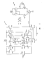
Fig. 4 has illustrated and has been applicable to and has the right operational amplifier of nmos differential 110 employed constant g
m/ C
LBiasing circuit 126.Operational amplifier 110 comprises the differential pair of a nmos device 112 and 114 and the differential pair of PMOS device 113 and 115, and they are connected in positive voltage source V in parallel
DDAnd between the node A.The right grid of nmos device links to each other with 118 with a pair of voltage input line 116 respectively.As shown in the figure, incoming line 120 links to each other with device 115 with node interconnection device 114.C is provided
LThe capacitor 120 of equivalent load capacitance output signal and external loading 121 are coupled.Operational amplifier work is poor with the free voltage that amplifies between the signal that receives along line 116 and 118.The output signal of representing these differences is along output line 120 outputs.Another nmos device 124 is connected between difference the NMOS right source electrode and ground, is used to receive offset signal and comes compensation process, temperature and bulk effect to change, and constant g still is provided
m/ C
L
In order to ensure producing offset signal, the voltage drop on the circuit 136 is essential.Thereby, provide voltage-setting circuitry in the biasing circuit 126.Voltage-setting circuitry comprises a pair of secondary nmos device 141 and 142, and its source electrode links to each other with ground, also comprises a pair of secondary PMOS device 144 and 146, and its source electrode links to each other with positive voltage source.The grid of secondary nmos device links together.The grid of secondary PMOS device links together and is attached to the grid of elementary PMOS device.The drain electrode of secondary PMOS device 144 is attached to Node B.The drain electrode of secondary nmos device 140 is attached to the grid of elementary nmos device 130. Secondary devices 142 and 146 drain electrode link together.At last, secondary nmos device 140 and 142 grid cross-couplings are to node D, with the drain electrode interconnection of device 142 and 146.Adopt this structure, various secondary nmos devices and PMOS device all have the function of current mirror, the voltage on the equivalent electrical circuit that is used to have a resistance, thus guarantee electric current by SC resistor equivalent electrical circuit.
Like this, the biasing circuit of Fig. 4 comprises the equivalent resistance circuit that is driven by the fixed frequency sampled clock signal, but not in some conventional biasing circuit visible simple resistor device.Therefore, realized constant g
m/ C
LRather than only realize constant g
mMore particularly, the equivalent resistance that is provided by circuit 136 is:
F in the formula
sBe the sample frequency of two input clocks, C is the electric capacity of sampling capacitor 137.In this circuit, when stable state, g
mValue be 1/R, therefore
Perhaps,
Thereby the unity gain bandwidth of operational amplifier is set up by the sampling clock frequency, and it generally is very stable amount.By fixing unity gain bandwidth, make the Time Created of operational amplifier constant.Equally, w
0Fixing, thus do not need associated edge and extra power consumption.G in the bias generator
mAnd C
LAll be preferred g respectively into operational amplifier and load
mThe change in size pattern, thereby saving power.Equally, notice that biasing circuit does not need to use outer resistor of chip or the outer assembly of other chip, and can realize that it is able to programme by using the simple digital frequency divider.
In addition, owing to be, the threshold voltage of two elementary nmos devices is equated basically between the grid of elementary nmos device but not between a nmos device and ground, form equivalent resistance.Thereby, may cause g
m/ C
LThe above-mentioned bulk effect variation that changes with threshold voltage can not take place.Therefore, the g of circuit
m/ C
LBasically avoid except that temperature and process change the influence that the bulk effect based on threshold voltage difference changes.
In order further to reduce the g that causes by bulk effect
m/ C
LVariation, source follower also is provided.Source follower helps to reduce may be because the variation that the difference between the source voltage elementary nmos device of biasing circuit and the operational amplifier nmos device causes.Source follower comprises a pair of secondary nmos device 150 and 152, and its source electrode links to each other with ground, also comprises the single secondary PMOS device 154 that is connected between device 152 and the positive voltage source.Source follower comprises another nmos device 156 in addition, and as shown in the figure, it is connected between the drain electrode of positive voltage source and nmos device 150.The grid of device 156 links to each other with common mode voltage incoming line 158, is used to receive and the common mode voltage that offers the signal correction of operational amplifier along line 116.
Adopt this structure, source follower work so that the source voltage of the elementary nmos device of biasing circuit equate with the source voltage of operational amplifier nmos device.Therefore, the bias current signal that is produced by biasing circuit is not subjected to the influence that process and temperature variation and bulk effect change substantially, and bulk effect may cause the source voltage mismatch.Bias current line 138 makes the gate interconnection of the bias device 114 of the grid of secondary nmos device 150 and 152 and operational amplifier, is used for bias current is coupled to operational amplifier.
Like this, Fig. 4 has illustrated a biasing circuit, and it not only provides process and temperature variation all constant basically g
m/ C
L, also remedied bulk effect.In a particular embodiment, the breadth length ratio of elementary nmos device 128 and elementary PMOS device 132 and 134 is W/L, and the breadth length ratio of elementary nmos device 130 is 4W/L.The breadth length ratio of secondary nmos device also is 4W/L.The breadth length ratio of secondary PMOS device is W/ L.Device 152 and 154 breadth length ratio are W/L.The breadth length ratio of device 150 is 5W/L, and the breadth length ratio of device 156 is 2W/L.
As mentioned above, the biasing circuit of Fig. 4 comprises single equivalent resistance circuit.Fig. 5 has illustrated another embodiment 126 ', and wherein parallel connection provides a pair of equivalent resistance circuit to help reduce parasitic capacitance effect.The biasing circuit of Fig. 5 is similar to the biasing circuit of Fig. 4, only describes relevant difference below in detail.
The biasing circuit of Fig. 5 comprises a pair of equivalent resistance circuit 136
1With 136
2The equivalent resistance circuit comprises sampling capacitor 137 respectively
1With 137
2, and the both has a pair of input clock signal switch 139
1With 139
2And 140
1With 140
2 Input clock switch 139
1With 139
2Receive fixed frequency non-overlapping clock sampled signal ck1 and ck2 respectively.Input clock switch 140
1With 140
2Receive fixed frequency non-overlapping clock sampled signal ck2 and ck1 respectively.Like this, the biasing circuit of Fig. 5 comprises a pair of equivalent resistance circuit, has reciprocal sampling clock ck1 and ck2.According to this configuration, when the switched capacitor of another circuit is discharging, will load the switched capacitor of the first equivalent resistance circuit, vice versa.
Fig. 6 and 7 has illustrated that the operational amplifier of SC circuit or other comprise the biasing circuit of the right employed stray-insensitive of device of nmos differential.Fig. 6 and 7 biasing circuit are similar to the biasing circuit of Figure 4 and 5, will describe only difference in detail below.Components identical is with adding that 100 reference number represents.
The stray insensitive bias circuit of Fig. 6 comprises that it has the single equivalent resistance circuit 236 of two ck1 signal inputs and two ck2 signal inputs, and the single switch capacitor.More particularly, equivalent resistance circuit 236 comprises the switched capacitor 237 that is connected between a pair of ck1 clock signal input 239A and the 239B, and the clock signal input links to each other with 230 grid with elementary nmos device 228 respectively again.Circuit 236 comprises a pair of ck2 signal input 240A and 240B in addition, and they are connected to node E to another terminal of capacitor 237, and as shown in the figure, node E is connected to the source electrode of elementary nmos device.
Adopt this structure, when ck1 activated, switched capacitor 237 was coupled with the grid of elementary nmos device.Yet when clock signal ck2 activated, the source electrode of switched capacitor and elementary nmos device was coupled.Therefore, provide a kind of symmetrical structure, and the variation in the clock signal can not cause any net change in the offset signal that is produced by biasing circuit.Therefore, the basic strays-insensitive of biasing circuit.
Fig. 7 has illustrated stray insensitive bias circuit 226 ', and the circuit of it and Fig. 6 is similar, but wherein provides a pair of equivalent resistance circuit to reduce parasitic capacitance effect.In brief, a pair of equivalent resistance circuit 236
1With 236
2In parallel.Equivalent resistance circuit 236
1The capacitor 237 that comprises independent switch
1And a pair of ck1 clock input switch 239A
1And 239B
1And a pair of ck2 clock switch 240A
1And 240B
1, they are as the figure configuration.Equivalent resistance circuit 237
2The capacitor 237 that comprises independent switch
2And a pair of ck2 clock input switch 239A
2And 239B
2And a pair of ck1 clock input switch 240A
2And 240B
2, they are as the figure configuration.Circuit 236
1 Switch 239A
1And 239B
1Receive the ck1 clock signal, and circuit 236
2 Switch 239A
2And 239B
2Receive the ck2 clock signal.Equally, circuit 236
1 Switch 240A
1And 240B
1Receive the ck2 clock signal, and circuit 236
2 Switch 240A
2And 240B
2Receive the ck1 clock signal.
Therefore, the biasing circuit of Fig. 7 provides a pair of balanced impedance equivalent electrical circuit, has the mutually anticlockwise input that is used for any effect that basic elimination may cause by stray capacitance.
The constant g that adopts a pair of fixing non-overlapped input clock signal has been described so
m/ C
LThe various embodiment of biasing circuit, clock signal is used for switched capacitor to set up equivalent resistance.Below with reference to Fig. 8 one embodiment is described, has wherein adopted input clock signal ck1, ck2 and the ck3 of three non-overlapping copies.Fig. 8 biasing circuit be similar to the biasing circuit of Fig. 4-7, relevant difference only is described below.Equally, components identical is represented with the reference number that increases by 100.
Fig. 8 has illustrated and has been applicable to operational amplifier 310 employed biasing circuits 326 that wherein biasing circuit comprises the single equivalent resistance circuit 336 with single switch capacitor 337.Yet, being different from equivalent resistance circuit and switched capacitor directly coupling between the grid of the elementary nmos device of biasing circuit in the foregoing description, the equivalent resistance circuit of the biasing circuit of Fig. 8 may separate.More particularly, switched capacitor 337 is connected a pair of ck1 clock signal input switch 339A and 339B, a pair of ck2 clock input switch 341A and 341B, reaches between a pair of ck3 clock input switch 343A and the 343B.The output of the operational amplifier that provides along line 320 links to each other with ck1 switch 339A.The common mode voltage signal input of input nmos device 358 also links to each other with ck1 switch 339B.The positive voltage reference signal that offers operational amplifier along line 318 also links to each other with ck2 clock switch 341A.Ck3 clock switch 343A links to each other with ground with 343B.At last, the positive and negative voltage reference signal that provides along line 316 and 318 also all links to each other with 330 grid with elementary nmos device 328 respectively.
Adopt this structure, the unity gain bandwidth operational amplifier is determined that by the sampling clock frequency this is a very stable amount.For saving power, the g in the bias generator
mWith sampling capacitor C
LAll can be selected as operational amplifier g
mTime variation with load.Like this, above-mentioned analysis is at least stable state and has realized constant g
m/ C
LAccording to implementation, nonlinear effect may take place before reaching stable state.Yet these nonlinear effects can not influence the g of final foundation substantially
m/ C
LBiasing.
Illustrated that like this, operational amplifier or other adopt the employed constant g of device of differential pair
m/ C
LThe various improvement of biasing circuit.Mainly discussed and adopt difference NMOS relevant device.These improvements can be eliminated substantially and may be changed or the caused variation of bulk effect by temperature variation, process.The further feature and the advantage of circuit also may be provided.In adopting the right device of difference PMOS, also can utilize these improvement.In this respect, in above-mentioned various circuit, may replace nmos device with the PMOS device, vice versa.Yet particular device size, operating voltage etc. may be different for the realization of difference PMOS.
The description of above preferred embodiment makes those skilled in the art can make or use the present invention.The various modifications of these embodiment are conspicuous for a person skilled in the art, and Ding Yi General Principle can be applied among other embodiment and not need to use creativity here.Therefore, the embodiment that the present invention is not limited to illustrate here, and will meet and the principle and the novel feature the most wide in range consistent scope that disclose here.
Claims (20)
1. biasing circuit that is used to add inclined to one side differential pair, described biasing circuit comprises:
Be used to produce the device of the source electric current of the pair of transistor device that comprises gate interconnection;
Be used for forming between the right grid of described transistor device the device of equivalent resistance, the described device that is used to form equivalent resistance comprises and is used to provide the device of electric capacity and provides the device of electric capacity optionally to be coupled to the right described grid of described transistor device to set up the device of equivalent resistance with fixing predetermined sampling frequency handle;
Apply the device of voltage at the described device two ends that are used to form equivalent resistance, make the described device that is used to produce the source electric current can also produce a bias current, this bias current is with proportional by the described formed resistance of device that is used to form resistance; And
Be used for bias current is applied to device on the differential pair.
2. biasing circuit as claimed in claim 1 is characterized in that described transistor device is a nmos device.
3. biasing circuit as claimed in claim 2 is characterized in that, the described device that is used to produce the source electric current comprises:
First and second nmos devices that between first and second nodes and ground, are connected in parallel respectively; And
The first and second PMOS devices that between first and second nodes and positive voltage source, are connected in parallel respectively; Wherein
The grid of described first and second nmos devices links together and further is connected to first node;
The grid of the described first and second PMOS devices links together and further is connected to Section Point.
4. biasing circuit as claimed in claim 3 is characterized in that, the described device that is used to form equivalent resistance comprises:
Capacitor links to each other between sampling node that connects described first and second nmos devices and ground; And
The input of first clock is connected between the described grid of sampling node and described first nmos device, and the second clock input, is connected between the described grid of the sampling node and second nmos device; Wherein
Described first and second clocks input provides the non-overlapping clock signal with preset sampling frequency.
5. biasing circuit as claimed in claim 3 is characterized in that, the described device that is used to form resistance comprises:
First capacitor links to each other between first sampling node of the grid that connects described first and second nmos devices and ground; And
The input of first clock is connected between the grid of first sampling node and described first nmos device, and the second clock input, is connected between the described grid of first sampling node and described second nmos device;
Second capacitor links to each other between second sampling node of the grid that connects described first and second nmos devices and ground; And
The second clock input is connected between the described grid of second sampling node and described first nmos device, and the input of first clock, is connected between the described grid of second sampling node and described second nmos device, wherein
Described first and second clocks input provides the non-overlapping clock signal with preset sampling frequency.
6. biasing circuit as claimed in claim 3 is characterized in that, the described device that is used to form resistance comprises:
Capacitor is connected between the grid of described first and second nmos devices; And
First clock input is connected between the described grid of first end of described capacitor and described first nmos device, and is connected between the described grid of second end of described capacitor and described second nmos device;
The second clock input is connected between first end and ground of described capacitor, and is connected between second end and described ground of described capacitor, and wherein said first and second clocks input provides the non-overlapping clock signal with preset sampling frequency.
7. biasing circuit as claimed in claim 3 is characterized in that, the described device that is used to form resistance comprises:
First capacitor is connected between the grid of described first and second nmos devices; And
First clock input is connected between the described grid of first end of described first capacitor and described first nmos device, and is connected between the described grid of second end of described first capacitor and described second nmos device;
The second clock input is connected between first end and ground of described first capacitor, and is connected between second end and described ground of described first capacitor;
Second capacitor is connected between the grid of described first and second nmos devices;
Second clock input is connected between the described grid of first end of described second capacitor and described first nmos device, and is connected between the described grid of second end of described second capacitor and described second nmos device;
The input of first clock is connected between first end and ground of described second capacitor, and is connected between second end and described ground of described second capacitor; Wherein
Described first and second clocks input provides the non-overlapping clock signal with preset sampling frequency.
8. biasing circuit as claimed in claim 3 is characterized in that, comprises being used to form the described device that applies voltage on the described device of resistance:
The 3rd nmos device is connected between the grid and ground of described second nmos device;
The 4th nmos device is connected between the 3rd node and the ground;
The 3rd PMOS device is connected between first node and the positive voltage source; And
The 4th PMOS device is connected between the 3rd node and the positive voltage source; Wherein
The grid of third and fourth nmos device links together and further is connected to the 3rd node.
9. biasing circuit as claimed in claim 1 is characterized in that, the described device that is used for bias voltage is put on differential pair comprises:
Offset line is used for the right source electrode of current source device is connected to differential pair.
10. one kind is applicable to differential pair is added inclined to one side biasing circuit, and described biasing circuit is characterised in that and comprises:
The a pair of current source device of gate interconnection;
The equivalent resistance circuit, be used between the right grid of described current source device, forming equivalent resistance, and the equivalent resistance circuit comprises sampling capacitor and on-off circuit, and the latter is used for fixing predetermined sampling frequency sampling capacitor being coupled to the right grid of current source device, to set up equivalent resistance;
With the voltage-setting circuitry that described equivalent resistance circuit links to each other, be used on described equivalent resistance circuit, applying a voltage; And
Offset line; Be used for voltage is exported from current source device being connected to differential pair.
11. biasing circuit as claimed in claim 10 is characterized in that, described equivalent resistance circuit comprises:
Capacitor links to each other connecting between right sampling node of described current source device and the ground; And
The input of first clock, be connected between sampling node and described first current source device, and the second clock input, being connected between sampling node and described second current source device, wherein said first and second clocks input provides the non-overlapping clock signal with preset sampling frequency.
12. biasing circuit as claimed in claim 10 is characterized in that, described equivalent resistance circuit comprises:
Capacitor is connected between the grid of described first and second current source devices; And
First clock input is connected between the described grid of first end of described capacitor and described first current source device, and is connected between the described grid of second end of described capacitor and described second current source device;
The second clock input is connected between first end and ground of described capacitor, and is connected between second end and described ground of described capacitor; Wherein
Described first and second clocks input provides the non-overlapping clock signal with preset sampling frequency.
13. biasing circuit as claimed in claim 10 is characterized in that, described current source device is to comprising first and second nmos devices.
14. biasing circuit as claimed in claim 13 is characterized in that, described equivalent resistance circuit comprises:
First capacitor is connected between the grid of described first and second nmos devices; And
First clock input is connected between the described grid of first end of described first capacitor and described first nmos device, and is connected between the described grid of second end of described first capacitor and described second nmos device;
The second clock input is connected between first end and ground of described first capacitor, and is connected between second end and described ground of described first capacitor;
Second capacitor is connected between the grid of described first and second nmos devices;
The 3rd clock input is connected between the described grid of first end of described second capacitor and described first nmos device, and is connected between the described grid of second end of described second capacitor and described second nmos device;
The input of the 4th clock is connected between first end and ground of described second capacitor, and is connected between second end and described ground of described second capacitor; Wherein
Described first and second clocks input provides the non-overlapping clock signal with preset sampling frequency, and the input of described third and fourth clock provides the non-overlapping clock signal with preset sampling frequency.
15. biasing circuit as claimed in claim 13 is characterized in that, described current source device is to comprising first and second nmos devices that are connected in parallel respectively between first and second nodes and ground; And
Wherein said biasing circuit also comprises the first and second PMOS devices that are connected in parallel respectively between first and second nodes and positive voltage source; Wherein
The grid of described first and second nmos devices links together and further links to each other with first node; And wherein
The grid of the described first and second PMOS devices links together and further links to each other with Section Point.
16. biasing circuit as claimed in claim 15 is characterized in that, described voltage-setting circuitry comprises:
The 3rd nmos device is connected between the grid and ground of described first nmos device;
The 4th nmos device is connected between the 3rd node and the ground;
The 3rd PMOS device is connected between first node and the positive voltage source; And
The 4th PMOS device is connected between the 3rd node and the positive voltage source; Wherein
The grid of third and fourth nmos device links together and further is connected to the 3rd node; And
The grid of the third and fourth PMOS device links together and further is connected to Section Point.
17. biasing circuit as claimed in claim 16 is characterized in that, described differential pair comprises:
The the 5th and the 6th nmos device that between the 4th node and positive voltage source, is connected in parallel, wherein the 5th links to each other with first and second incoming lines respectively with the grid of the 6th nmos device; And
Be connected the 7th nmos device between the 4th node and the ground, wherein the grid of the 7th nmos device links to each other with biasing circuit by offset line.
18. biasing circuit as claimed in claim 15 is characterized in that, described offset line links to each other with the 5th node, and the 5th node is connected between first and second nmos devices and the ground.
19. biasing circuit as claimed in claim 13 is characterized in that, also comprises the source follower that links to each other with the source electrode of first and second nmos devices, wherein source follower has the grid voltage that is arranged on the right common mode voltage of input difference.
20. biasing circuit as claimed in claim 19 is characterized in that, described source follower comprises:
The 8th nmos device link to each other between the source electrode of positive voltage source and first and second nmos devices, and its grid links to each other with the common mode voltage incoming line;
The 9th nmos device is connected between the source electrode and ground of first and second nmos devices;
The tenth nmos device and the 5th PMOS device are connected in series between positive voltage source and the ground; Wherein
The 9th links together with the grid of the tenth nmos device and links to each other with the 6th node, and the 6th node is connected between the 5th PMOS device and the tenth nmos device; And
The drain electrode of the 9th nmos device is connected to the source electrode of third and fourth nmos device.
Applications Claiming Priority (2)
| Application Number | Priority Date | Filing Date | Title |
|---|---|---|---|
| US09/773,404 | 2001-01-31 | ||
| US09/773,404 US6407623B1 (en) | 2001-01-31 | 2001-01-31 | Bias circuit for maintaining a constant value of transconductance divided by load capacitance |
Publications (2)
| Publication Number | Publication Date |
|---|---|
| CN1555517A CN1555517A (en) | 2004-12-15 |
| CN100380266C true CN100380266C (en) | 2008-04-09 |
Family
ID=25098165
Family Applications (1)
| Application Number | Title | Priority Date | Filing Date |
|---|---|---|---|
| CNB028061764A Expired - Fee Related CN100380266C (en) | 2001-01-31 | 2002-01-30 | Bias circuit for maintaining a constant value of transconductance divided by load capacitance |
Country Status (9)
| Country | Link |
|---|---|
| US (1) | US6407623B1 (en) |
| EP (1) | EP1356356A2 (en) |
| JP (1) | JP4422408B2 (en) |
| CN (1) | CN100380266C (en) |
| BR (1) | BR0206834A (en) |
| CA (1) | CA2437193C (en) |
| HK (1) | HK1070146A1 (en) |
| IL (2) | IL157141A (en) |
| WO (1) | WO2002061519A2 (en) |
Cited By (1)
| Publication number | Priority date | Publication date | Assignee | Title |
|---|---|---|---|---|
| CN104898751A (en) * | 2014-03-09 | 2015-09-09 | 财团法人交大思源基金会 | Bias circuit |
Families Citing this family (34)
| Publication number | Priority date | Publication date | Assignee | Title |
|---|---|---|---|---|
| CA2166450C (en) * | 1995-01-20 | 2008-03-25 | Ronald Salovey | Chemically crosslinked ultrahigh molecular weight polyethylene for artificial human joints |
| AU2002349859A1 (en) * | 2002-10-15 | 2004-06-07 | Agency For Science, Technology And Research | Apparatus and method for implementing a constant transconductance circuit |
| US6946896B2 (en) * | 2003-05-29 | 2005-09-20 | Broadcom Corporation | High temperature coefficient MOS bias generation circuit |
| JP2006146916A (en) * | 2004-11-22 | 2006-06-08 | Samsung Sdi Co Ltd | Current mirror circuit, drive circuit and drive method using the same |
| EP1679795B1 (en) * | 2005-01-10 | 2016-10-26 | CSEM Centre Suisse d'Electronique et de Microtechnique SA - Recherche et Développement | Biasing circuit structure for continuous time filters |
| CN100386706C (en) * | 2005-02-25 | 2008-05-07 | 清华大学 | Bias compensation circuit for adjusting transconductance variation range of transistor in load |
| US20060226892A1 (en) * | 2005-04-12 | 2006-10-12 | Stmicroelectronics S.A. | Circuit for generating a reference current |
| US7265625B2 (en) * | 2005-10-04 | 2007-09-04 | Analog Devices, Inc. | Amplifier systems with low-noise, constant-transconductance bias generators |
| US7307476B2 (en) * | 2006-02-17 | 2007-12-11 | Semiconductor Components Industries, L.L.C. | Method for nullifying temperature dependence and circuit therefor |
| WO2008050375A1 (en) * | 2006-09-29 | 2008-05-02 | Fujitsu Limited | Bias circuit |
| US7741827B2 (en) * | 2007-05-01 | 2010-06-22 | Semiconductor Components Industries, Llc | Parameter control circuit including charging and discharging current mirrors and method therefor |
| US8044654B2 (en) | 2007-05-18 | 2011-10-25 | Analog Devices, Inc. | Adaptive bias current generator methods and apparatus |
| CN101471632B (en) * | 2007-12-26 | 2011-07-20 | 中国科学院微电子研究所 | Self-bias low-voltage operation transconductance amplifier circuit with controllable loop gain |
| TWI435543B (en) * | 2008-02-06 | 2014-04-21 | Mediatek Inc | Semiconductor circuit and method for mitigating current variation in a semiconductor circuit |
| EP2124125A1 (en) * | 2008-05-21 | 2009-11-25 | Seiko Epson Corporation | Process and temperature compensation in CMOS circuits |
| US7750837B2 (en) * | 2008-08-01 | 2010-07-06 | Qualcomm Incorporated | Adaptive bias current generation for switched-capacitor circuits |
| US7982526B2 (en) * | 2008-09-17 | 2011-07-19 | Qualcomm, Incorporated | Active-time dependent bias current generation for switched-capacitor circuits |
| JP5515708B2 (en) * | 2009-12-11 | 2014-06-11 | 富士通株式会社 | Bias circuit and amplifier circuit having the same |
| US8390371B2 (en) * | 2010-07-30 | 2013-03-05 | Tialinx, Inc. | Tunable transconductance-capacitance filter with coefficients independent of variations in process corner, temperature, and input supply voltage |
| JP2012119835A (en) * | 2010-11-30 | 2012-06-21 | Asahi Kasei Electronics Co Ltd | Active filter |
| CN102969990A (en) * | 2011-09-01 | 2013-03-13 | 联咏科技股份有限公司 | Multi-input differential amplifier with dynamic transduction compensation |
| CN102437820B (en) * | 2011-12-21 | 2014-11-26 | 苏州云芯微电子科技有限公司 | Clock amplifier circuit for lowering introduction of phase noise |
| US9194890B2 (en) * | 2013-05-09 | 2015-11-24 | Freescale Semiconductor, Inc. | Metal-oxide-semiconductor (MOS) voltage divider with dynamic impedance control |
| CN104796092B (en) * | 2014-01-22 | 2018-02-13 | 上海华虹集成电路有限责任公司 | Equalizing circuit |
| CN104579206B (en) * | 2014-07-30 | 2017-08-08 | 上海华虹宏力半导体制造有限公司 | Differential amplifier circuit and operational amplifier |
| US10359794B2 (en) | 2014-10-13 | 2019-07-23 | Qorvo Us, Inc. | Switched capacitor biasing circuit |
| JP2016122897A (en) * | 2014-12-24 | 2016-07-07 | 三菱電機株式会社 | Divider circuit |
| EP3487076A1 (en) * | 2017-11-15 | 2019-05-22 | ams AG | Phase-locked loop circuitry having low variation transconductance design |
| CN108566173A (en) * | 2018-06-11 | 2018-09-21 | 杨俊杰 | A kind of RC time constant correcting circuits using CMOS technology chip interior |
| CN109672418A (en) * | 2018-12-19 | 2019-04-23 | 佛山臻智微芯科技有限公司 | A kind of high gain operational amplifier using feedforward compensation |
| CN109639135B (en) * | 2019-01-22 | 2024-03-01 | 上海艾为电子技术股份有限公司 | Charge pump circuit |
| US11251759B2 (en) | 2020-01-30 | 2022-02-15 | Texas Instruments Incorporated | Operational amplifier input stage with high common mode voltage rejection |
| KR20220046116A (en) | 2020-10-07 | 2022-04-14 | 삼성전자주식회사 | Amplifier and electronic device including amplifier |
| CN114265461A (en) * | 2021-12-15 | 2022-04-01 | 深圳飞骧科技股份有限公司 | Reference voltage source |
Citations (5)
| Publication number | Priority date | Publication date | Assignee | Title |
|---|---|---|---|---|
| US5444362A (en) * | 1991-12-20 | 1995-08-22 | Goldstar Electron Co., Ltd. | Dual back-bias voltage generating circuit with switched outputs |
| US5550510A (en) * | 1994-12-27 | 1996-08-27 | Lucent Technologies Inc. | Constant transconductance CMOS amplifier input stage with rail-to-rail input common mode voltage range |
| US5594382A (en) * | 1992-10-20 | 1997-01-14 | Fujitsu Ltd. | Constant voltage circuit |
| CN1201294A (en) * | 1997-05-16 | 1998-12-09 | 松下电器产业株式会社 | Reactive-current-trimmed power amplifier and trimming method thereof |
| US6144249A (en) * | 1998-01-15 | 2000-11-07 | Chrontel, Inc. | Clock-referenced switching bias current generator |
Family Cites Families (10)
| Publication number | Priority date | Publication date | Assignee | Title |
|---|---|---|---|---|
| GB2213011B (en) * | 1987-09-16 | 1991-09-25 | Philips Electronic Associated | A method of and a circuit arrangement for processing sampled analogue electricals |
| US5656957A (en) * | 1995-10-19 | 1997-08-12 | Sgs-Thomson Microelectronics, Inc. | Comparator circuit with hysteresis |
| JP3348019B2 (en) * | 1998-07-06 | 2002-11-20 | シャープ株式会社 | Pulse wave amplifier |
| JP2000040924A (en) * | 1998-07-24 | 2000-02-08 | Nec Corp | Constant current drive circuit |
| JP2000039926A (en) * | 1998-07-24 | 2000-02-08 | Canon Inc | Current outputting circuit |
| JP2953465B1 (en) * | 1998-08-14 | 1999-09-27 | 日本電気株式会社 | Constant current drive circuit |
| JP4508425B2 (en) * | 1998-12-17 | 2010-07-21 | コーニンクレッカ フィリップス エレクトロニクス エヌ ヴィ | Circuit equipment |
| US6323725B1 (en) * | 1999-03-31 | 2001-11-27 | Qualcomm Incorporated | Constant transconductance bias circuit having body effect cancellation circuitry |
| JP4015319B2 (en) * | 1999-07-12 | 2007-11-28 | 富士通株式会社 | Constant current generation circuit and differential amplifier circuit |
| US6300805B1 (en) * | 1999-09-30 | 2001-10-09 | Texas Instruments Incorporated | Circuit for auto-zeroing a high impedance CMOS current driver |
-
2001
- 2001-01-31 US US09/773,404 patent/US6407623B1/en not_active Expired - Lifetime
-
2002
- 2002-01-30 JP JP2002562029A patent/JP4422408B2/en not_active Expired - Fee Related
- 2002-01-30 WO PCT/US2002/003012 patent/WO2002061519A2/en active Application Filing
- 2002-01-30 IL IL157141A patent/IL157141A/en not_active IP Right Cessation
- 2002-01-30 CN CNB028061764A patent/CN100380266C/en not_active Expired - Fee Related
- 2002-01-30 BR BR0206834-6A patent/BR0206834A/en not_active IP Right Cessation
- 2002-01-30 CA CA002437193A patent/CA2437193C/en not_active Expired - Fee Related
- 2002-01-30 EP EP02702128A patent/EP1356356A2/en not_active Withdrawn
-
2005
- 2005-03-30 HK HK05102656A patent/HK1070146A1/en not_active IP Right Cessation
-
2008
- 2008-09-24 IL IL194326A patent/IL194326A/en not_active IP Right Cessation
Patent Citations (5)
| Publication number | Priority date | Publication date | Assignee | Title |
|---|---|---|---|---|
| US5444362A (en) * | 1991-12-20 | 1995-08-22 | Goldstar Electron Co., Ltd. | Dual back-bias voltage generating circuit with switched outputs |
| US5594382A (en) * | 1992-10-20 | 1997-01-14 | Fujitsu Ltd. | Constant voltage circuit |
| US5550510A (en) * | 1994-12-27 | 1996-08-27 | Lucent Technologies Inc. | Constant transconductance CMOS amplifier input stage with rail-to-rail input common mode voltage range |
| CN1201294A (en) * | 1997-05-16 | 1998-12-09 | 松下电器产业株式会社 | Reactive-current-trimmed power amplifier and trimming method thereof |
| US6144249A (en) * | 1998-01-15 | 2000-11-07 | Chrontel, Inc. | Clock-referenced switching bias current generator |
Cited By (1)
| Publication number | Priority date | Publication date | Assignee | Title |
|---|---|---|---|---|
| CN104898751A (en) * | 2014-03-09 | 2015-09-09 | 财团法人交大思源基金会 | Bias circuit |
Also Published As
| Publication number | Publication date |
|---|---|
| WO2002061519A2 (en) | 2002-08-08 |
| CA2437193C (en) | 2009-05-26 |
| US6407623B1 (en) | 2002-06-18 |
| WO2002061519A3 (en) | 2002-12-05 |
| JP4422408B2 (en) | 2010-02-24 |
| CA2437193A1 (en) | 2002-08-08 |
| CN1555517A (en) | 2004-12-15 |
| EP1356356A2 (en) | 2003-10-29 |
| IL157141A0 (en) | 2004-02-08 |
| HK1070146A1 (en) | 2005-06-10 |
| IL157141A (en) | 2010-06-30 |
| BR0206834A (en) | 2004-12-28 |
| IL194326A (en) | 2010-11-30 |
| JP2004523830A (en) | 2004-08-05 |
Similar Documents
| Publication | Publication Date | Title |
|---|---|---|
| CN100380266C (en) | Bias circuit for maintaining a constant value of transconductance divided by load capacitance | |
| US6552611B2 (en) | Differential amplifier and filter circuit using the same | |
| KR100299740B1 (en) | Filter circuit | |
| US6344767B1 (en) | Switched-opamp technique for low-voltage switched capacitor circuits | |
| JP2007159117A (en) | Low voltage low power class a/b output stage | |
| Bhaskar et al. | New CFOA-based sinusoidal oscillators retaining independent control of oscillation frequency even under the influence of parasitic impedances | |
| KR19980081642A (en) | Variable gain amplifier | |
| US20090184752A1 (en) | Bias circuit | |
| US6370066B1 (en) | Differential output circuit | |
| BAŞAK et al. | Ultra-low voltage VDBA design by using PMOS DTMOS transistors | |
| Arslan et al. | Self-biasing current conveyor for high frequency applications | |
| US9231540B2 (en) | High performance class AB operational amplifier | |
| Pretl et al. | Fifty nifty variations of two-transistor circuits: A tribute to the versatility of MOSFETs | |
| US8035448B1 (en) | Differential amplifier that compensates for process variations | |
| Wu et al. | A CMOS OTA with improved linearity based on current addition | |
| CN211352180U (en) | Oscillation circuit and clock circuit | |
| US6507246B1 (en) | FET circuit with resistor-programmable transconductance | |
| Chaichana et al. | A new quadrature sinusoidal oscillator for telecommunication system using VDDDAs | |
| CN210405229U (en) | Preamplifier, pre-differential amplifier, and integrated circuit | |
| Aggarwal et al. | Design of temperature and input voltage insensitive VDTA and impedance multiplier | |
| JP2009118258A (en) | Voltage-current conversion circuit | |
| Obaid et al. | Design of a CMOS differential operational transresistance amplifier in 90 nm CMOS technology | |
| Supreetha et al. | A Novel Design of Tunable and Balanced VDIBA | |
| JP2021164055A (en) | Fully differential amplifier | |
| Khatib et al. | Obvody pro analogové zpracování signálů na bázi nekonvenčních aktivních prvků |
Legal Events
| Date | Code | Title | Description |
|---|---|---|---|
| C06 | Publication | ||
| PB01 | Publication | ||
| C10 | Entry into substantive examination | ||
| SE01 | Entry into force of request for substantive examination | ||
| REG | Reference to a national code |
Ref country code: HK Ref legal event code: DE Ref document number: 1070146 Country of ref document: HK |
|
| C14 | Grant of patent or utility model | ||
| GR01 | Patent grant | ||
| REG | Reference to a national code |
Ref country code: HK Ref legal event code: GR Ref document number: 1070146 Country of ref document: HK |
|
| C17 | Cessation of patent right | ||
| CF01 | Termination of patent right due to non-payment of annual fee |
Granted publication date: 20080409 Termination date: 20110130 |