CN100336181C - Precise patterning of high-k films - Google Patents
Precise patterning of high-k films Download PDFInfo
- Publication number
- CN100336181C CN100336181C CNB2004100708261A CN200410070826A CN100336181C CN 100336181 C CN100336181 C CN 100336181C CN B2004100708261 A CNB2004100708261 A CN B2004100708261A CN 200410070826 A CN200410070826 A CN 200410070826A CN 100336181 C CN100336181 C CN 100336181C
- Authority
- CN
- China
- Prior art keywords
- dielectric constant
- grid
- material layer
- high dielectric
- dielectric material
- Prior art date
- Legal status (The legal status is an assumption and is not a legal conclusion. Google has not performed a legal analysis and makes no representation as to the accuracy of the status listed.)
- Expired - Fee Related
Links
- 238000000059 patterning Methods 0.000 title abstract description 7
- 239000000463 material Substances 0.000 claims abstract description 58
- 238000000034 method Methods 0.000 claims abstract description 48
- UFHFLCQGNIYNRP-UHFFFAOYSA-N Hydrogen Chemical compound [H][H] UFHFLCQGNIYNRP-UHFFFAOYSA-N 0.000 claims abstract description 21
- 239000003989 dielectric material Substances 0.000 claims description 76
- 229910052751 metal Inorganic materials 0.000 claims description 39
- 239000002184 metal Substances 0.000 claims description 39
- 239000000758 substrate Substances 0.000 claims description 35
- 239000001257 hydrogen Substances 0.000 claims description 26
- 229910052739 hydrogen Inorganic materials 0.000 claims description 26
- 239000000126 substance Substances 0.000 claims description 25
- MHAJPDPJQMAIIY-UHFFFAOYSA-N Hydrogen peroxide Chemical compound OO MHAJPDPJQMAIIY-UHFFFAOYSA-N 0.000 claims description 14
- VEXZGXHMUGYJMC-UHFFFAOYSA-N Hydrochloric acid Chemical compound Cl VEXZGXHMUGYJMC-UHFFFAOYSA-N 0.000 claims description 8
- 229910000449 hafnium oxide Inorganic materials 0.000 claims description 7
- WIHZLLGSGQNAGK-UHFFFAOYSA-N hafnium(4+);oxygen(2-) Chemical compound [O-2].[O-2].[Hf+4] WIHZLLGSGQNAGK-UHFFFAOYSA-N 0.000 claims description 7
- 150000002431 hydrogen Chemical class 0.000 claims description 7
- QAOWNCQODCNURD-UHFFFAOYSA-N Sulfuric acid Chemical compound OS(O)(=O)=O QAOWNCQODCNURD-UHFFFAOYSA-N 0.000 claims description 6
- MCMNRKCIXSYSNV-UHFFFAOYSA-N ZrO2 Inorganic materials O=[Zr]=O MCMNRKCIXSYSNV-UHFFFAOYSA-N 0.000 claims description 6
- RVTZCBVAJQQJTK-UHFFFAOYSA-N oxygen(2-);zirconium(4+) Chemical compound [O-2].[O-2].[Zr+4] RVTZCBVAJQQJTK-UHFFFAOYSA-N 0.000 claims description 6
- 229910052735 hafnium Inorganic materials 0.000 claims description 5
- VBJZVLUMGGDVMO-UHFFFAOYSA-N hafnium atom Chemical compound [Hf] VBJZVLUMGGDVMO-UHFFFAOYSA-N 0.000 claims description 5
- 241000252506 Characiformes Species 0.000 claims description 4
- QCWXUUIWCKQGHC-UHFFFAOYSA-N Zirconium Chemical compound [Zr] QCWXUUIWCKQGHC-UHFFFAOYSA-N 0.000 claims 3
- 229910052726 zirconium Inorganic materials 0.000 claims 3
- 230000008569 process Effects 0.000 abstract description 9
- 230000015572 biosynthetic process Effects 0.000 abstract description 3
- 239000010409 thin film Substances 0.000 abstract 1
- 238000001039 wet etching Methods 0.000 description 12
- 238000005530 etching Methods 0.000 description 8
- 238000005516 engineering process Methods 0.000 description 7
- 238000006722 reduction reaction Methods 0.000 description 6
- 238000004377 microelectronic Methods 0.000 description 5
- 238000005240 physical vapour deposition Methods 0.000 description 4
- 238000005260 corrosion Methods 0.000 description 3
- 230000007797 corrosion Effects 0.000 description 3
- 239000004065 semiconductor Substances 0.000 description 3
- XKRFYHLGVUSROY-UHFFFAOYSA-N Argon Chemical compound [Ar] XKRFYHLGVUSROY-UHFFFAOYSA-N 0.000 description 2
- 230000008859 change Effects 0.000 description 2
- 238000006243 chemical reaction Methods 0.000 description 2
- 239000011248 coating agent Substances 0.000 description 2
- 238000000576 coating method Methods 0.000 description 2
- 238000001312 dry etching Methods 0.000 description 2
- 238000012986 modification Methods 0.000 description 2
- 230000004048 modification Effects 0.000 description 2
- 229910021420 polycrystalline silicon Inorganic materials 0.000 description 2
- 229920005591 polysilicon Polymers 0.000 description 2
- 150000004760 silicates Chemical class 0.000 description 2
- 229910052710 silicon Inorganic materials 0.000 description 2
- 239000010703 silicon Substances 0.000 description 2
- KCXVZYZYPLLWCC-UHFFFAOYSA-N EDTA Chemical compound OC(=O)CN(CC(O)=O)CCN(CC(O)=O)CC(O)=O KCXVZYZYPLLWCC-UHFFFAOYSA-N 0.000 description 1
- ABLZXFCXXLZCGV-UHFFFAOYSA-N Phosphorous acid Chemical class OP(O)=O ABLZXFCXXLZCGV-UHFFFAOYSA-N 0.000 description 1
- 229910052581 Si3N4 Inorganic materials 0.000 description 1
- 239000000654 additive Substances 0.000 description 1
- 230000000996 additive effect Effects 0.000 description 1
- 239000007864 aqueous solution Substances 0.000 description 1
- 229910052786 argon Inorganic materials 0.000 description 1
- 239000002738 chelating agent Substances 0.000 description 1
- 238000004140 cleaning Methods 0.000 description 1
- 238000010276 construction Methods 0.000 description 1
- 238000004090 dissolution Methods 0.000 description 1
- 229960001484 edetic acid Drugs 0.000 description 1
- 239000007789 gas Substances 0.000 description 1
- 239000001307 helium Substances 0.000 description 1
- 229910052734 helium Inorganic materials 0.000 description 1
- SWQJXJOGLNCZEY-UHFFFAOYSA-N helium atom Chemical compound [He] SWQJXJOGLNCZEY-UHFFFAOYSA-N 0.000 description 1
- 239000011261 inert gas Substances 0.000 description 1
- 150000002739 metals Chemical class 0.000 description 1
- 239000007800 oxidant agent Substances 0.000 description 1
- 230000001590 oxidative effect Effects 0.000 description 1
- 230000000737 periodic effect Effects 0.000 description 1
- 230000009467 reduction Effects 0.000 description 1
- 230000000717 retained effect Effects 0.000 description 1
- HQVNEWCFYHHQES-UHFFFAOYSA-N silicon nitride Chemical compound N12[Si]34N5[Si]62N3[Si]51N64 HQVNEWCFYHHQES-UHFFFAOYSA-N 0.000 description 1
- 125000006850 spacer group Chemical group 0.000 description 1
- 229910052723 transition metal Inorganic materials 0.000 description 1
- 150000003624 transition metals Chemical class 0.000 description 1
Images


Classifications
-
- H—ELECTRICITY
- H01—ELECTRIC ELEMENTS
- H01L—SEMICONDUCTOR DEVICES NOT COVERED BY CLASS H10
- H01L21/00—Processes or apparatus adapted for the manufacture or treatment of semiconductor or solid state devices or of parts thereof
- H01L21/02—Manufacture or treatment of semiconductor devices or of parts thereof
- H01L21/04—Manufacture or treatment of semiconductor devices or of parts thereof the devices having potential barriers, e.g. a PN junction, depletion layer or carrier concentration layer
- H01L21/18—Manufacture or treatment of semiconductor devices or of parts thereof the devices having potential barriers, e.g. a PN junction, depletion layer or carrier concentration layer the devices having semiconductor bodies comprising elements of Group IV of the Periodic Table or AIIIBV compounds with or without impurities, e.g. doping materials
- H01L21/30—Treatment of semiconductor bodies using processes or apparatus not provided for in groups H01L21/20 - H01L21/26
- H01L21/302—Treatment of semiconductor bodies using processes or apparatus not provided for in groups H01L21/20 - H01L21/26 to change their surface-physical characteristics or shape, e.g. etching, polishing, cutting
- H01L21/306—Chemical or electrical treatment, e.g. electrolytic etching
- H01L21/3063—Electrolytic etching
-
- H—ELECTRICITY
- H01—ELECTRIC ELEMENTS
- H01L—SEMICONDUCTOR DEVICES NOT COVERED BY CLASS H10
- H01L21/00—Processes or apparatus adapted for the manufacture or treatment of semiconductor or solid state devices or of parts thereof
- H01L21/02—Manufacture or treatment of semiconductor devices or of parts thereof
- H01L21/04—Manufacture or treatment of semiconductor devices or of parts thereof the devices having potential barriers, e.g. a PN junction, depletion layer or carrier concentration layer
- H01L21/18—Manufacture or treatment of semiconductor devices or of parts thereof the devices having potential barriers, e.g. a PN junction, depletion layer or carrier concentration layer the devices having semiconductor bodies comprising elements of Group IV of the Periodic Table or AIIIBV compounds with or without impurities, e.g. doping materials
- H01L21/28—Manufacture of electrodes on semiconductor bodies using processes or apparatus not provided for in groups H01L21/20 - H01L21/268
- H01L21/28008—Making conductor-insulator-semiconductor electrodes
- H01L21/28017—Making conductor-insulator-semiconductor electrodes the insulator being formed after the semiconductor body, the semiconductor being silicon
- H01L21/28026—Making conductor-insulator-semiconductor electrodes the insulator being formed after the semiconductor body, the semiconductor being silicon characterised by the conductor
- H01L21/28123—Lithography-related aspects, e.g. sub-lithography lengths; Isolation-related aspects, e.g. to solve problems arising at the crossing with the side of the device isolation; Planarisation aspects
-
- H—ELECTRICITY
- H01—ELECTRIC ELEMENTS
- H01L—SEMICONDUCTOR DEVICES NOT COVERED BY CLASS H10
- H01L21/00—Processes or apparatus adapted for the manufacture or treatment of semiconductor or solid state devices or of parts thereof
- H01L21/02—Manufacture or treatment of semiconductor devices or of parts thereof
- H01L21/04—Manufacture or treatment of semiconductor devices or of parts thereof the devices having potential barriers, e.g. a PN junction, depletion layer or carrier concentration layer
- H01L21/18—Manufacture or treatment of semiconductor devices or of parts thereof the devices having potential barriers, e.g. a PN junction, depletion layer or carrier concentration layer the devices having semiconductor bodies comprising elements of Group IV of the Periodic Table or AIIIBV compounds with or without impurities, e.g. doping materials
- H01L21/30—Treatment of semiconductor bodies using processes or apparatus not provided for in groups H01L21/20 - H01L21/26
- H01L21/31—Treatment of semiconductor bodies using processes or apparatus not provided for in groups H01L21/20 - H01L21/26 to form insulating layers thereon, e.g. for masking or by using photolithographic techniques; After treatment of these layers; Selection of materials for these layers
- H01L21/3105—After-treatment
- H01L21/311—Etching the insulating layers by chemical or physical means
- H01L21/31105—Etching inorganic layers
- H01L21/31111—Etching inorganic layers by chemical means
Landscapes
- Engineering & Computer Science (AREA)
- Physics & Mathematics (AREA)
- Condensed Matter Physics & Semiconductors (AREA)
- General Physics & Mathematics (AREA)
- Manufacturing & Machinery (AREA)
- Computer Hardware Design (AREA)
- Microelectronics & Electronic Packaging (AREA)
- Power Engineering (AREA)
- Chemical & Material Sciences (AREA)
- Chemical Kinetics & Catalysis (AREA)
- General Chemical & Material Sciences (AREA)
- Inorganic Chemistry (AREA)
- Insulated Gate Type Field-Effect Transistor (AREA)
- Drying Of Semiconductors (AREA)
- Weting (AREA)
- Electrodes Of Semiconductors (AREA)
- Laminated Bodies (AREA)
- Insulating Bodies (AREA)
Abstract
A high-K thin film patterning solution is disclosed to address structural and process limitations of conventional patterning techniques. Subsequent to formation of gate structures adjacent a high-K dielectric layer, a portion of the high-K dielectric layer material is reduced, preferably via exposure to hydrogen gas, to form a reduced portion of the high-K dielectric layer. The reduced portion may be selectively removed utilizing wet etch chemistries to leave behind a trench of desirable geometric properties.
Description
Technical field
The present invention relates to make microelectronic component, more specifically, relate to the accurate formation of groove in the dielectric layer.
Background technology
By cambium layer and groove in the various structure constructions of making by various materials, can produce microelectronic structure such as semiconductor structure.With being used to that the dielectric film such as high-k (or " high K ") film is carried out a relevant challenge of the conventional art of patterning is accurately to form groove, to avoid the infringement to the integrality of adjacent structure.With reference to Figure 1A, described the cross-sectional view of typical grid structure, wherein with high-K gate oxide skin(coating) 102 adjacent two grids 104,106 with wall 108,110,112,114 that formed, wherein high-K gate oxide skin(coating) 102 adjacent substrate layers 100 form.Figure 1B has described unfavorable patterning situation, has wherein used dry etching technology, causes dark groove 116.Although the relative anisotropic properties of dry etching technology helps minimizing negative etching deviation, but they may be accompanied by the difficulty in the degree of depth that the control groove forms, for example describe as Figure 1B, wherein groove 116 has extended in the substrate layer 100 undesirablely.Fig. 1 C illustrates another kind of unfavorable patterning situation, has wherein used wet etching, has caused the incision of undesirable ground (undercut) groove 118 of proximity structure, and these proximity structures for example are grid 104,106 and wall 110,112.Many wet etching treatment are associated with isotropic substantially etch rate characteristic, cause negative etching deviation and incision, for example describe as Fig. 1 C.
Summary of the invention
According to an aspect of the present invention, provide a kind of method, having comprised: on substrate material layer, formed the high dielectric constant dielectric material layer; On described high dielectric constant dielectric material layer, form first grid and second grid at least, reserve the expose portion of the described high dielectric constant material between described first and second grids; The described expose portion of described high dielectric constant dielectric material layer is exposed to hydrogen, reduces described expose portion, to form the metal part by described expose portion; By described metal partly is exposed to described metal is partly had optionally wet chemical etchant, remove described metal part, to form groove from described high dielectric constant material layer; Form the wall adjacent with described second grid with described first grid; And wherein, the step that forms described wall comprises, remove described metal part branch from described high dielectric constant material layer after, forms the described wall adjacent with described grid.
According to another aspect of the present invention, provide a kind of method, having comprised: on substrate, formed the high dielectric constant dielectric material layer; On described high dielectric constant dielectric material layer, form first grid and second grid at least, reserve the expose portion of the described high dielectric constant material between described first and second grids; The described expose portion of described high dielectric constant dielectric material layer is exposed to hydrogen, reduces the described expose portion of described high dielectric constant dielectric material layer, to form the metal part by described expose portion; By described metal partly is exposed to described metal partly had optionally wet chemical etchant, remove described metal part from described high dielectric constant material layer, between described first grid and described second grid, to form groove, on the side opposite of described first and second grids, reserve the discontinuous part of described high dielectric constant material simultaneously with described groove; Form first wall on the side adjacent with described groove of described first grid, described first wall extends to the described groove from the upper surface of described grid basically, reaches the lower surface of described groove; And on the side opposite of described first grid, forming second wall with described groove, described second wall extends to the described discontinuous part of described high dielectric constant material basically from the upper surface of described grid.
According to another aspect of the present invention, provide a kind of method, having comprised: on substrate material layer, formed the high dielectric constant dielectric material layer; On described high dielectric constant dielectric material layer, form first grid and second grid at least, reserve the expose portion of the described high dielectric constant material between described first and second grids, each of wherein said first grid and described second grid has lower surface; The described expose portion of described high dielectric constant dielectric material layer is exposed to hydrogen, reduces described expose portion, to form the metal part by described expose portion; By described metal partly is exposed to described metal is partly had optionally wet chemical etchant, remove described metal part, between described first grid and described second grid, to form groove from described high dielectric constant material layer; Form first side adjacent first wall adjacent with described groove with described first grid, the position of described first wall on the lower surface of described first grid extends to the described groove, reaches the position under the lower surface of described first grid.
According to another aspect of the present invention, provide a kind of device, having comprised: substrate material layer; High dielectric constant dielectric material layer on described substrate material layer, described high dielectric constant dielectric material layer is divided into first and second portion by groove; First grid in the described first of described high dielectric constant dielectric material; Second grid on the described second portion of described high dielectric constant dielectric material; With with first side adjacent first wall adjacent of described first grid with described groove, the position of described first wall on the lower surface of described first grid extends to the described groove, reaches the position under the upper surface of described first of described high dielectric constant dielectric material.
Description of drawings
The present invention is illustrated explanation by way of example, and the invention is not restricted to the figure in the accompanying drawing, and similar in the drawings mark is represented similar elements.Feature shown in the accompanying drawing is not defined as in proportion and draws, and is not defined as with accurate position relation to illustrate yet.
Figure 1A~Fig. 1 C is that the cross section of traditional underlay pattern processing is described;
Fig. 2 A~Fig. 2 C is the cross-sectional view of each side of the patterned process of the embodiment of the invention;
Fig. 3 is the flow chart in each stage of describing the patterned process of the embodiment of the invention;
Fig. 4 A~Fig. 4 D is the cross-sectional view of each side of the patterned process of second embodiment of the invention;
Fig. 5 is the flow chart in each stage of describing the patterned process of second embodiment of the invention.
Embodiment
In the detailed description to the embodiment of the invention, with reference to accompanying drawing, wherein similar mark is represented similar elements below.Illustrative examples described here is by fully at length open, so that those skilled in the art can implement the present invention.Therefore following detailed description does not have the meaning of restriction, and scope of the present invention is only defined by claims.
Fig. 2 A~Fig. 2 C is the cross-sectional view of each side of the patterned process of one embodiment of the present of invention.With reference to figure 2A, show with Figure 1A in the similar microelectronic structure described.Can utilize various technology and material to form such structure.For example, can use, on substrate layer 100, form high-k dielectrics layer 102 such as chemistry or physical vapour deposition (PVD) or other technology.In each embodiment, high-k dielectrics layer 102 can comprise the hafnium such as hafnium oxide, zirconium dioxide or its silicate derivative, and substrate layer 100 can comprise the semi-conducting material such as silicon or other material.Subsequently, can between wall 108,110,112,114, form grid 104,106.In one embodiment, the grid material that grid 104,106 comprises such as polysilicon, the material spacer layer that wall 108,110,112,114 comprises such as silicon nitride is although also can use other materials in other embodiments.After forming grid 104,106 and wall 108,110,112,114, the part 132 on high-k dielectrics layer 102 surface keeps exposing.
With reference to figure 2B, the high-k dielectrics laminar surface 132 of exposure is exposed to hydrogen 120, produces hydrogen reduction reaction.Using hydrogen molecule that d district (in the periodic table of elements between II family and the III family) transition metal complex/film is reduced to the corresponding metal element is a kind of known phenomenon, for instance, described in the publication of the second edition of for example writing as N.N.Greenwood in 1997 and A.Earnshaw " Chemistry ofthe Elements ".Hydrogen, easily penetrates in such film on its direction that is applied in anisotropic substantially mode, to the degree of depth that runs into usually in high K microelectronic component structure, such as arriving between about 100 dusts at about 5 dusts.
In one embodiment, in the parallel-plate plasma chamber, the surface 132 that exposes is exposed to hydrogen 120, comprising grid 104,106, the device wafer of high-k dielectrics layer 102 and substrate layer 100 is as a pole plate, and separates about 5mm with second pole plate and arrive interval in the scope of about 10mm.Have radio frequency (" RF ") power source, it has about 2W/cm
2To about 4W/cm
2Power density in the scope and about 200KHz are to the interior frequency of about 13.5MHz scope.Chip temperature from about 20 ℃ in about 450 ℃ scope.Have about 1000SCCM to the interior hydrogen flowing quantity of about 2000SCCM scope, and about 0SCCM is to the interior inert gas flow such as argon gas or helium of about 2000SCCM scope.The pressure of this chamber holds in the palm in the scope of about 2 holders about 1.Other embodiment can use different conditions to carry out the hydrogen reducing reaction.
High-K gate dielectric 102 comprises among the embodiment of hafnium oxide therein, and the hydrogen reducing reaction can followingly be represented:
HfO
2+2H
2→Hf+2H
2O
Reduction reaction obtains the part 122 that high-K gate dielectric layer 102 is reduced.Describe as Fig. 2 C, be now metallics be reduced or " by change " part 122 can have optionally wet etching chemicals 124 to metal by being exposed to through changing, optionally removed, to stay groove 126, wherein wet etching chemicals 124 for example is the etch chemistry based on sulfuric acid and hydrogen peroxide that is known as " piranha " etch chemistry, perhaps is known as the etch chemistry based on hydrochloric acid and hydrogen peroxide of " SC2 " or " RCA standard cleaning 2 " wet etching chemicals.The removal of reduction part 122 also produces the discontinuous part 128,130 of remaining high-k dielectrics layer 102.Because the selectivity high relatively that in contrast to other adjacent nonmetallic materials of such wet etching chemicals 124 to metallics, the negative basically etching deviation of groove 126 or to the infringement of following substrate layer 100, described other adjacent nonmetallic materials comprise the part of the adjacent high-K gate dielectric 102 that is not reduced or is changed.In fact, the material 122 that is reduced by removal and the groove 126 that obtains is straight basically has substantially parallel wall---and this also is known as in the art, and to have be the groove of zero plus or minus " etching deviation " substantially.Such as the wet etching chemicals 124 of piranha and SC2,, be known in the art as being used for optionally removing organic substance and metal to arrive the system of following metal or backing material.For example, having the low pH system of oxidant, such as the hydrochloric acid with hydrogen peroxide of picture in the SC2 etch chemistry, is a kind of known effective ways of dissolution of metals.In other embodiments, can use additive method, for example, optionally remove the part 122 that is reduced such as the common chelating agent aqueous solution of phosphonates derivative or ethylenediamine tetra-acetic acid.Thereby dielectric layer 102 is by patternization accurately, avoided the adjacent problem such as the structure of grid 104,106 or wall 108,110,112,114 of substrate layer 100 below the corrosion and incision.
With reference to figure 3, described to sum up the flow chart of the patterned process of one embodiment of the invention, wherein, the adjacent substrate layer forms 300 high-K gate dielectric layers, thereafter contiguous high-K gate dielectric layer forms 302 grids and wall, reserves the surface of the exposure of high-K gate dielectric layer.The high-K gate dielectric layer surface of this exposure is exposed to 304 hydrogen that cause reduction reaction.By the high-K gate dielectric substance that is reduced is had optionally wet etching chemicals, the high-K gate dielectric substance that etching 306 is reduced, to form groove, make that the gate dielectric material be reduced is optionally removed, and substantially can incision not adjacent grid structure or can not corrode following substrate layer material substantially.
Fig. 4 A~Fig. 4 D is the cross-sectional view of each side of the patterned process of second embodiment of the invention.With reference to figure 4A, show with Fig. 2 A in the similar microelectronic structure described.But the structure among Fig. 4 A does not comprise the wall 108,110,112,114 adjacent with grid 104,106.Can use various technology and material to form such structure.For example, can use, on substrate layer 100, form high-k dielectrics layer 102 such as chemistry or physical vapour deposition (PVD) or other technology.In each embodiment, high-k dielectrics layer 102 can comprise the hafnium such as hafnium oxide, zirconium dioxide or its silicate derivative, and substrate layer 100 can comprise the semi-conducting material such as silicon or other material.Subsequently, can on high-k dielectrics layer 102, form grid 104,106.In one embodiment, the grid material that grid 104,106 comprises such as polysilicon is although also can use other materials in other embodiments.After forming grid 104,106, the part 132 of the high-k dielectrics layer 102 between grid 104,106 keeps exposing.
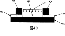
With reference to figure 4B, the high-k dielectrics laminar surface 132 of exposure is exposed to hydrogen 120, produces hydrogen reduction reaction.In one embodiment, this exposure of being carried out is to top similar about the described exposure of Fig. 2 B, obtains the identical result of the part 122 that high-K gate dielectric layer 102 is reduced.Describe as Fig. 4 C, be now metallics be reduced or " by change " part 122 can have optionally wet etching chemicals 124 to metal by being exposed to through changing, by the removal of selectivity, to stay groove 126.This wet etching chemicals 124 is generally finished function with top about the described identical mode of Fig. 2 C.The removal that is reduced part 122 also produces remaining high-k dielectrics layer 102 remaining discontinuous part 128,130.Because the selectivity high relatively that in contrast to other adjacent nonmetallic materials of such wet etching chemicals 124 to metallics, the negative basically etching deviation of groove 126 or to the infringement of following substrate layer 100, described other adjacent nonmetallic materials comprise the part of the adjacent high-K gate dielectric 102 that is not reduced or is changed.In fact, the material 122 that is reduced by removal and the groove 126 that obtains is straight basically has substantially parallel wall---and this also is known as in this area, and to have be the groove of zero plus or minus " etching deviation " substantially.Thereby dielectric layer 102 is by patternization accurately, avoided the adjacent problem such as the structure of grid 104,106 of substrate layer 100 below the corrosion and incision.
With reference to figure 4D, then with the discontinuous part 128,130 and grid 104, the 106 adjacent formation walls 108,110,112,114 of high-k dielectrics layer 102.Shown in Fig. 4 D, the discontinuous part 128,130 of the contiguous high-k dielectrics layers 102 of wall 110,112 and grid 104,106 both and form, and the upper surface from grid 104,106 extends to the groove 126 basically, and to by on the upper surface that is reduced the material that part 122 is exposed of removing high-k dielectrics layer 102.The upper surface that is reduced the material that part 122 is exposed by removing the high-k dielectrics layer is the lower surface of groove 126, and this is the upper surface of substrate layer 100 in illustrated embodiment.In illustrated embodiment, on a side of each grid 104,106, form groove 126.High-k dielectrics layer 102 is retained on the non-channel side of grid 104,106.In such embodiments, wall 108,114 adjacent gate 104,106 on the non-channel side of grid 104,106 are formed, and extend to the upper surface of the discontinuous part 128,130 of high-k dielectrics layer 102 basically from the upper surface of grid 104,106.But in other embodiment (not shown), groove 126 can be formed on in the grid 104,106 one or boths' the both sides.In other these embodiment, discontinuous part 128,130 and grid 104,106 that one of wall 108,114 on the non-channel side of grid 104,106 or both also can be close to high-k dielectrics layer 102 are formed, and the upper surface from grid 104,106 extends to the groove 126 basically, and to by removing the upper surface that is reduced the substrate layer 100 that part 122 is exposed of high-k dielectrics layer 102.Thereby dielectric layer 102 is by patternization accurately, avoided the adjacent problem such as the structure of grid 104,106 or wall 108,110,112,114 of substrate layer 100 below the corrosion and incision.
With reference to figure 5, described to sum up the flow chart of the patterned process of one embodiment of the invention, wherein the adjacent substrate layer forms 500 high-K gate dielectric layers, and contiguous thereafter high-K gate dielectric layer forms 502 grids, reserves the surface that is exposed of high-K gate dielectric layer.The high-K gate dielectric layer surface of this exposure is exposed 504 to the hydrogen that causes reduction reaction.By the high-K gate dielectric substance that is reduced is had optionally wet etching chemicals, the high-K gate dielectric substance that etching 506 is reduced, to form groove, make that the gate dielectric material be reduced is optionally removed, and substantially can incision not adjacent grid structure or can not corrode following substrate layer material substantially.Then, a part and the grid that is close to remaining high-K gate dielectric layer forms 508 walls.On the side of grid adjacent trenches, these walls extend to the upper surface of substrate layer basically from the upper surface of grid.
The underlay pattern that so discloses a kind of novelty is dissolved certainly method.Though with reference to certain embodiments the present invention has been described here, those of ordinary skill in the art will easily expect many modifications wherein.Therefore, all such changes and modifications are all comprised by in the determined protection range that the invention is intended to of claims.
Claims (41)
1. method comprises:
On substrate material layer, form the high dielectric constant dielectric material layer;
On described high dielectric constant dielectric material layer, form first grid and second grid at least, reserve the expose portion of the described high dielectric constant material between described first and second grids;
The described expose portion of described high dielectric constant dielectric material layer is exposed to hydrogen, reduces described expose portion, to form the metal part by described expose portion;
By described metal partly is exposed to described metal is partly had optionally wet chemical etchant, remove described metal part, to form groove from described high dielectric constant material layer;
Form the wall adjacent with described second grid with described first grid; And
Wherein, the step that forms described wall comprises, remove described metal part branch from described high dielectric constant material layer after, forms the described wall adjacent with described grid.
2. the method for claim 1, wherein at least one described wall basically from described first and second grids one upper surface extend in the described groove, reach the lower surface of described groove.
3. the method for claim 1, the step that wherein forms described wall comprises, before the described expose portion with described high dielectric constant dielectric material layer is exposed to hydrogen, forms described wall.
4. method as claimed in claim 3, wherein said wall extend to the upper surface of described high dielectric constant dielectric material layer basically from the upper surface of the grid adjacent with described wall.
5. the method for claim 1, wherein said high dielectric constant dielectric material comprises hafnium oxide, and wherein said metal part branch comprises hafnium.
6. the method for claim 1, wherein said high dielectric constant dielectric material comprises zirconium dioxide, and wherein said metal part branch comprises zirconium.
7. the method for claim 1, the step that wherein the described expose portion of described high dielectric constant dielectric material layer is exposed to hydrogen comprises that the described expose portion with described high dielectric constant dielectric material layer in plasma chamber is exposed to hydrogen.
8. method as claimed in claim 7, wherein said high dielectric constant dielectric material layer is placed in the described plasma chamber with the distance from the scope of pole plate from about 5mm to about 10mm.
9. method as claimed in claim 7, the step that wherein the described expose portion of described high dielectric constant dielectric material layer is exposed to hydrogen comprises, the described expose portion of described high dielectric constant dielectric material layer is exposed to the hydrogen of range of flow from about 1000SCCM to about 2000SCCM.
10. method comprises:
On substrate, form the high dielectric constant dielectric material layer;
On described high dielectric constant dielectric material layer, form first grid and second grid at least, reserve the expose portion of the described high dielectric constant material between described first and second grids;
The described expose portion of described high dielectric constant dielectric material layer is exposed to hydrogen, reduces the described expose portion of described high dielectric constant dielectric material layer, to form the metal part by described expose portion;
By described metal partly is exposed to described metal partly had optionally wet chemical etchant, remove described metal part from described high dielectric constant material layer, between described first grid and described second grid, to form groove, on the side opposite of described first and second grids, reserve the discontinuous part of described high dielectric constant material simultaneously with described groove;
Form first wall on the side adjacent with described groove of described first grid, described first wall extends to the described groove from the upper surface of described grid basically, reaches the lower surface of described groove; And
Form second wall on the side opposite with described groove of described first grid, described second wall extends to the described discontinuous part of described high dielectric constant material basically from the upper surface of described grid.
11. method as claimed in claim 10, wherein said high dielectric constant dielectric material comprises hafnium oxide, and wherein said metal part branch comprises hafnium.
12. method as claimed in claim 10, wherein said high dielectric constant dielectric material comprises zirconium dioxide, and wherein said metal part branch comprises zirconium.
13. method as claimed in claim 10, the step that wherein the described expose portion of described high dielectric constant dielectric material layer is exposed to hydrogen comprises that the described expose portion with described high dielectric constant dielectric material layer in plasma chamber is exposed to hydrogen.
14. method as claimed in claim 13, wherein said high dielectric constant dielectric material layer is placed in the described plasma chamber with the distance from the scope of pole plate from about 5mm to about 10mm.
15. method as claimed in claim 13, the step that wherein the described expose portion of described high dielectric constant dielectric material layer is exposed to hydrogen comprises, the described expose portion of described high dielectric constant dielectric material layer is exposed to the hydrogen of range of flow from about 1000SCCM to about 2000SCCM.
16. method as claimed in claim 10, wherein said wet chemical etchant comprises the etch chemistry based on sulfuric acid and hydrogen peroxide.
17. method as claimed in claim 16, wherein said etch chemistry are the piranha etch chemistry.
18. method as claimed in claim 10, wherein said wet chemical etchant comprises the etch chemistry based on hydrochloric acid and hydrogen peroxide.
19. method as claimed in claim 18, wherein said etch chemistry are the SC2 etch chemistry.
20. a method comprises:
On substrate material layer, form the high dielectric constant dielectric material layer;
On described high dielectric constant dielectric material layer, form first grid and second grid at least, reserve the expose portion of the described high dielectric constant material between described first and second grids, each of wherein said first grid and described second grid has lower surface;
The described expose portion of described high dielectric constant dielectric material layer is exposed to hydrogen, reduces described expose portion, to form the metal part by described expose portion;
By described metal partly is exposed to described metal is partly had optionally wet chemical etchant, remove described metal part, between described first grid and described second grid, to form groove from described high dielectric constant material layer;
Form first side adjacent first wall adjacent with described groove with described first grid, the position of described first wall on the lower surface of described first grid extends to the described groove, reaches the position under the lower surface of described first grid.
21. method as claimed in claim 20, wherein said wet chemical etchant comprises the etch chemistry based on sulfuric acid and hydrogen peroxide.
22. method as claimed in claim 21, wherein said etch chemistry are the piranha etch chemistry.
23. method as claimed in claim 20, wherein said wet chemical etchant comprises the etch chemistry based on hydrochloric acid and hydrogen peroxide.
24. method as claimed in claim 23, wherein said etch chemistry are the SC2 etch chemistry.
25. method as claimed in claim 20, wherein said high dielectric constant dielectric material comprises hafnium oxide, and wherein said metal part branch comprises hafnium.
26. method as claimed in claim 20, wherein said high dielectric constant dielectric material comprises zirconium dioxide, and wherein said metal part branch comprises zirconium.
27. method as claimed in claim 20, wherein said first wall extends to the lower surface of described groove.
28. method as claimed in claim 20, wherein form after the described groove between described first and second grids, the part of described high dielectric constant material layer is left the discontinuous part on second side opposite with described first side of described first grid.
29. method as claimed in claim 28 also comprises the second adjacent wall of described second side that forms with described first grid, described second wall extends to described discontinuous part from the position on the lower surface of described first grid.
30. method as claimed in claim 20, the step of wherein removing described metal part is reserved the expose portion of described backing material in the bottom of described groove.
31. method as claimed in claim 30, wherein said first wall extends to described backing material.
32. method as claimed in claim 31, wherein between described first and second grids, form after the described groove, the part of described high dielectric constant dielectric material layer is left the discontinuous part on second side opposite with described first side of described first grid, and described method also comprises the second adjacent wall of described second side that forms with described first grid, and described second wall extends to described discontinuous part from the position on the lower surface of described first grid.
33. a device comprises:
Substrate material layer;
High dielectric constant dielectric material layer on described substrate material layer, described high dielectric constant dielectric material layer is divided into first and second portion by groove;
First grid in the described first of described high dielectric constant dielectric material;
Second grid on the described second portion of described high dielectric constant dielectric material; With
First side adjacent first wall adjacent with described first grid with described groove, the position of described first wall on the lower surface of described first grid extends to the described groove, reaches the position under the upper surface of described first of described high dielectric constant dielectric material.
34. device as claimed in claim 33, wherein said groove have the sidewall that extends towards described substrate material layer from the upper surface of described high dielectric constant dielectric material layer, described sidewall is straight substantially, and parallel to each other substantially.
35. device as claimed in claim 33, wherein said groove has the sidewall that extends to the upper surface of described substrate material layer from the upper surface of described high dielectric constant dielectric material layer.
36. the device shown in claim 35, the regional substantially flat of the described upper surface of wherein said substrate material layer, described zone are included in the part of the substrate material layer under the described groove and the part of the substrate material layer under described first and second parts of described high dielectric constant dielectric material.
37. device as claimed in claim 36, wherein said sidewall are straight substantially, and parallel to each other substantially.
38. device as claimed in claim 37, wherein said high dielectric constant dielectric material comprises the material of selecting from the group of being made up of hafnium oxide and zirconium dioxide.
39. device as claimed in claim 33, wherein said first wall extend to the bottom of described groove from the position on the lower surface of described first grid.
40. device as claimed in claim 33, wherein said first wall extend to the upper surface of described substrate material layer from the position on the lower surface of described first grid.
41. device as claimed in claim 33 also comprises second wall adjacent with second side of described first grid, described second wall extends to the upper surface of described high dielectric constant dielectric material layer from the position on the lower surface of described first grid.
Applications Claiming Priority (2)
| Application Number | Priority Date | Filing Date | Title |
|---|---|---|---|
| US10/632,470 US6855639B1 (en) | 2003-08-01 | 2003-08-01 | Precise patterning of high-K films |
| US10/632,470 | 2003-08-01 |
Publications (2)
| Publication Number | Publication Date |
|---|---|
| CN1581446A CN1581446A (en) | 2005-02-16 |
| CN100336181C true CN100336181C (en) | 2007-09-05 |
Family
ID=33541545
Family Applications (1)
| Application Number | Title | Priority Date | Filing Date |
|---|---|---|---|
| CNB2004100708261A Expired - Fee Related CN100336181C (en) | 2003-08-01 | 2004-07-20 | Precise patterning of high-k films |
Country Status (8)
| Country | Link |
|---|---|
| US (2) | US6855639B1 (en) |
| EP (1) | EP1503404B1 (en) |
| KR (1) | KR100592841B1 (en) |
| CN (1) | CN100336181C (en) |
| AT (1) | ATE450887T1 (en) |
| DE (1) | DE602004024355D1 (en) |
| TW (1) | TWI320204B (en) |
| WO (1) | WO2005013347A2 (en) |
Families Citing this family (15)
| Publication number | Priority date | Publication date | Assignee | Title |
|---|---|---|---|---|
| JP4040425B2 (en) * | 2002-10-17 | 2008-01-30 | Necエレクトロニクス株式会社 | Manufacturing method of semiconductor device |
| US20050064716A1 (en) * | 2003-04-14 | 2005-03-24 | Hong Lin | Plasma removal of high k metal oxide |
| US7413996B2 (en) * | 2003-04-14 | 2008-08-19 | Lsi Corporation | High k gate insulator removal |
| US7037845B2 (en) * | 2003-08-28 | 2006-05-02 | Intel Corporation | Selective etch process for making a semiconductor device having a high-k gate dielectric |
| US7160779B2 (en) * | 2005-02-23 | 2007-01-09 | Intel Corporation | Method for making a semiconductor device having a high-k gate dielectric |
| US20060220090A1 (en) * | 2005-03-23 | 2006-10-05 | Intel Corporation | Semiconductor device with a high-k gate dielectric and a metal gate electrode |
| US7449756B2 (en) * | 2005-06-13 | 2008-11-11 | Intel Corporation | Semiconductor device with a high-k gate dielectric and a metal gate electrode |
| US7501336B2 (en) * | 2005-06-21 | 2009-03-10 | Intel Corporation | Metal gate device with reduced oxidation of a high-k gate dielectric |
| US7595248B2 (en) * | 2005-12-01 | 2009-09-29 | Intel Corporation | Angled implantation for removal of thin film layers |
| US7226831B1 (en) | 2005-12-27 | 2007-06-05 | Intel Corporation | Device with scavenging spacer layer |
| US7984408B2 (en) * | 2006-04-21 | 2011-07-19 | International Business Machines Corporation | Structures incorporating semiconductor device structures with reduced junction capacitance and drain induced barrier lowering |
| US7659178B2 (en) * | 2006-04-21 | 2010-02-09 | International Business Machines Corporation | Semiconductor device structures with reduced junction capacitance and drain induced barrier lowering and methods for fabricating such device structures and for fabricating a semiconductor-on-insulator substrate |
| US20070262399A1 (en) * | 2006-05-10 | 2007-11-15 | Gilbert Dewey | Sealing spacer to reduce or eliminate lateral oxidation of a high-k gate dielectric |
| KR100973828B1 (en) * | 2008-05-09 | 2010-08-03 | 포항공과대학교 산학협력단 | Glass nano fabrication method using deposition of metal thin film |
| US8853076B2 (en) | 2012-09-10 | 2014-10-07 | International Business Machines Corporation | Self-aligned contacts |
Citations (2)
| Publication number | Priority date | Publication date | Assignee | Title |
|---|---|---|---|---|
| JPH0831314A (en) * | 1994-07-15 | 1996-02-02 | Canon Inc | Electron emitting element, electron source, image forming device using the source, and their manufacture |
| US6432779B1 (en) * | 2000-05-18 | 2002-08-13 | Motorola, Inc. | Selective removal of a metal oxide dielectric |
Family Cites Families (10)
| Publication number | Priority date | Publication date | Assignee | Title |
|---|---|---|---|---|
| JPS5424236A (en) * | 1977-07-25 | 1979-02-23 | Sharp Corp | Etching solution and minute working process |
| US4980032A (en) * | 1988-08-12 | 1990-12-25 | Alameda Instruments, Inc. | Distillation method and apparatus for reprocessing sulfuric acid |
| USRE35827E (en) * | 1989-05-02 | 1998-06-23 | Sgs-Thomson Microelectronics S.R.L. | Surface field effect transistor with depressed source and/or drain areas for ULSI integrated devices |
| US6124620A (en) * | 1998-05-14 | 2000-09-26 | Advanced Micro Devices, Inc. | Incorporating barrier atoms into a gate dielectric using gas cluster ion beam implantation |
| US6017790A (en) * | 1998-07-06 | 2000-01-25 | United Microelectronics Corp. | Method of manufacturing embedded dynamic random access memory |
| JP2001213696A (en) * | 1999-11-22 | 2001-08-07 | Shin Etsu Handotai Co Ltd | Manufacturing method of epitaxyial wafer and its semiconductor manufacturing equipment |
| US6300202B1 (en) * | 2000-05-18 | 2001-10-09 | Motorola Inc. | Selective removal of a metal oxide dielectric |
| US6544906B2 (en) * | 2000-12-21 | 2003-04-08 | Texas Instruments Incorporated | Annealing of high-k dielectric materials |
| US7887711B2 (en) * | 2002-06-13 | 2011-02-15 | International Business Machines Corporation | Method for etching chemically inert metal oxides |
| US6794721B2 (en) * | 2002-12-23 | 2004-09-21 | International Business Machines Corporation | Integration system via metal oxide conversion |
-
2003
- 2003-08-01 US US10/632,470 patent/US6855639B1/en not_active Expired - Lifetime
-
2004
- 2004-07-20 CN CNB2004100708261A patent/CN100336181C/en not_active Expired - Fee Related
- 2004-07-21 WO PCT/US2004/023568 patent/WO2005013347A2/en active Application Filing
- 2004-07-22 TW TW093121973A patent/TWI320204B/en not_active IP Right Cessation
- 2004-07-23 DE DE602004024355T patent/DE602004024355D1/en active Active
- 2004-07-23 AT AT04017471T patent/ATE450887T1/en not_active IP Right Cessation
- 2004-07-23 EP EP04017471A patent/EP1503404B1/en not_active Not-in-force
- 2004-07-30 KR KR1020040060505A patent/KR100592841B1/en not_active IP Right Cessation
- 2004-12-20 US US11/018,015 patent/US20050110072A1/en not_active Abandoned
Patent Citations (2)
| Publication number | Priority date | Publication date | Assignee | Title |
|---|---|---|---|---|
| JPH0831314A (en) * | 1994-07-15 | 1996-02-02 | Canon Inc | Electron emitting element, electron source, image forming device using the source, and their manufacture |
| US6432779B1 (en) * | 2000-05-18 | 2002-08-13 | Motorola, Inc. | Selective removal of a metal oxide dielectric |
Also Published As
| Publication number | Publication date |
|---|---|
| KR20050016077A (en) | 2005-02-21 |
| EP1503404B1 (en) | 2009-12-02 |
| WO2005013347A2 (en) | 2005-02-10 |
| EP1503404A3 (en) | 2005-04-06 |
| WO2005013347A3 (en) | 2005-04-28 |
| TWI320204B (en) | 2010-02-01 |
| CN1581446A (en) | 2005-02-16 |
| KR100592841B1 (en) | 2006-06-26 |
| EP1503404A2 (en) | 2005-02-02 |
| ATE450887T1 (en) | 2009-12-15 |
| US6855639B1 (en) | 2005-02-15 |
| US20050110072A1 (en) | 2005-05-26 |
| US20050026451A1 (en) | 2005-02-03 |
| TW200518224A (en) | 2005-06-01 |
| DE602004024355D1 (en) | 2010-01-14 |
Similar Documents
| Publication | Publication Date | Title |
|---|---|---|
| CN100336181C (en) | Precise patterning of high-k films | |
| US7368394B2 (en) | Etch methods to form anisotropic features for high aspect ratio applications | |
| US8294246B2 (en) | Semiconductor structures including square cuts in single crystal silicon and method of forming same | |
| US6071815A (en) | Method of patterning sidewalls of a trench in integrated circuit manufacturing | |
| US7709341B2 (en) | Methods of shaping vertical single crystal silicon walls and resulting structures | |
| JP4653735B2 (en) | Process for forming a dual metal gate structure | |
| US20070202700A1 (en) | Etch methods to form anisotropic features for high aspect ratio applications | |
| TWI447811B (en) | Methods for forming a conductive material, methods for selectively forming a conductive material, methods for forming platinum, and methods for forming conductive structures | |
| US9966312B2 (en) | Method for etching a silicon-containing substrate | |
| JP2008135534A (en) | Manufacturing method of semiconductor substrate comprising bottomed slot | |
| US6440858B1 (en) | Multi-layer hard mask for deep trench silicon etch | |
| US7732347B2 (en) | Semiconductor device and fabrication process of semiconductor device | |
| JPH10178014A (en) | Method for manufacturing semiconductor device | |
| CN104701145A (en) | Forming method of semiconductor structure | |
| CN100561671C (en) | The manufacture method of grating of semiconductor element | |
| US20200135898A1 (en) | Hard mask replenishment for etching processes | |
| US20050142826A1 (en) | Method for forming silicide film in semiconductor device | |
| KR100479231B1 (en) | Method for forming a silicide gate line in a semiconductor dual damascene structure | |
| JPH07135198A (en) | Etching | |
| JP2008108803A (en) | Method of cleaning semiconductor device | |
| KR100236078B1 (en) | Etching method for semiconductor material | |
| JP2006080353A (en) | Manufacturing method of semiconductor device | |
| KR20000000536A (en) | Trench forming method for semiconductor device |
Legal Events
| Date | Code | Title | Description |
|---|---|---|---|
| C06 | Publication | ||
| PB01 | Publication | ||
| C10 | Entry into substantive examination | ||
| SE01 | Entry into force of request for substantive examination | ||
| C14 | Grant of patent or utility model | ||
| GR01 | Patent grant | ||
| CF01 | Termination of patent right due to non-payment of annual fee |
Granted publication date: 20070905 Termination date: 20170720 |
|
| CF01 | Termination of patent right due to non-payment of annual fee |