WO2018194133A1 - Semiconductor substrate manufacturing method, semiconductor device, and method for manufacturing same - Google Patents
Semiconductor substrate manufacturing method, semiconductor device, and method for manufacturing same Download PDFInfo
- Publication number
- WO2018194133A1 WO2018194133A1 PCT/JP2018/016187 JP2018016187W WO2018194133A1 WO 2018194133 A1 WO2018194133 A1 WO 2018194133A1 JP 2018016187 W JP2018016187 W JP 2018016187W WO 2018194133 A1 WO2018194133 A1 WO 2018194133A1
- Authority
- WO
- WIPO (PCT)
- Prior art keywords
- diamine
- tetracarboxylic dianhydride
- polyimide
- aromatic
- layer
- Prior art date
Links
Images


Classifications
-
- H—ELECTRICITY
- H01—ELECTRIC ELEMENTS
- H01L—SEMICONDUCTOR DEVICES NOT COVERED BY CLASS H10
- H01L21/00—Processes or apparatus adapted for the manufacture or treatment of semiconductor or solid state devices or of parts thereof
- H01L21/02—Manufacture or treatment of semiconductor devices or of parts thereof
- H01L21/04—Manufacture or treatment of semiconductor devices or of parts thereof the devices having at least one potential-jump barrier or surface barrier, e.g. PN junction, depletion layer or carrier concentration layer
- H01L21/50—Assembly of semiconductor devices using processes or apparatus not provided for in a single one of the subgroups H01L21/06 - H01L21/326, e.g. sealing of a cap to a base of a container
- H01L21/56—Encapsulations, e.g. encapsulation layers, coatings
-
- H—ELECTRICITY
- H01—ELECTRIC ELEMENTS
- H01L—SEMICONDUCTOR DEVICES NOT COVERED BY CLASS H10
- H01L21/00—Processes or apparatus adapted for the manufacture or treatment of semiconductor or solid state devices or of parts thereof
- H01L21/67—Apparatus specially adapted for handling semiconductor or electric solid state devices during manufacture or treatment thereof; Apparatus specially adapted for handling wafers during manufacture or treatment of semiconductor or electric solid state devices or components ; Apparatus not specifically provided for elsewhere
- H01L21/683—Apparatus specially adapted for handling semiconductor or electric solid state devices during manufacture or treatment thereof; Apparatus specially adapted for handling wafers during manufacture or treatment of semiconductor or electric solid state devices or components ; Apparatus not specifically provided for elsewhere for supporting or gripping
- H01L21/6835—Apparatus specially adapted for handling semiconductor or electric solid state devices during manufacture or treatment thereof; Apparatus specially adapted for handling wafers during manufacture or treatment of semiconductor or electric solid state devices or components ; Apparatus not specifically provided for elsewhere for supporting or gripping using temporarily an auxiliary support
-
- C—CHEMISTRY; METALLURGY
- C09—DYES; PAINTS; POLISHES; NATURAL RESINS; ADHESIVES; COMPOSITIONS NOT OTHERWISE PROVIDED FOR; APPLICATIONS OF MATERIALS NOT OTHERWISE PROVIDED FOR
- C09J—ADHESIVES; NON-MECHANICAL ASPECTS OF ADHESIVE PROCESSES IN GENERAL; ADHESIVE PROCESSES NOT PROVIDED FOR ELSEWHERE; USE OF MATERIALS AS ADHESIVES
- C09J179/00—Adhesives based on macromolecular compounds obtained by reactions forming in the main chain of the macromolecule a linkage containing nitrogen, with or without oxygen, or carbon only, not provided for in groups C09J161/00 - C09J177/00
- C09J179/04—Polycondensates having nitrogen-containing heterocyclic rings in the main chain; Polyhydrazides; Polyamide acids or similar polyimide precursors
- C09J179/08—Polyimides; Polyester-imides; Polyamide-imides; Polyamide acids or similar polyimide precursors
-
- C—CHEMISTRY; METALLURGY
- C09—DYES; PAINTS; POLISHES; NATURAL RESINS; ADHESIVES; COMPOSITIONS NOT OTHERWISE PROVIDED FOR; APPLICATIONS OF MATERIALS NOT OTHERWISE PROVIDED FOR
- C09J—ADHESIVES; NON-MECHANICAL ASPECTS OF ADHESIVE PROCESSES IN GENERAL; ADHESIVE PROCESSES NOT PROVIDED FOR ELSEWHERE; USE OF MATERIALS AS ADHESIVES
- C09J5/00—Adhesive processes in general; Adhesive processes not provided for elsewhere, e.g. relating to primers
-
- H—ELECTRICITY
- H01—ELECTRIC ELEMENTS
- H01L—SEMICONDUCTOR DEVICES NOT COVERED BY CLASS H10
- H01L21/00—Processes or apparatus adapted for the manufacture or treatment of semiconductor or solid state devices or of parts thereof
- H01L21/02—Manufacture or treatment of semiconductor devices or of parts thereof
- H01L21/02104—Forming layers
- H01L21/02107—Forming insulating materials on a substrate
- H01L21/02109—Forming insulating materials on a substrate characterised by the type of layer, e.g. type of material, porous/non-porous, pre-cursors, mixtures or laminates
- H01L21/02112—Forming insulating materials on a substrate characterised by the type of layer, e.g. type of material, porous/non-porous, pre-cursors, mixtures or laminates characterised by the material of the layer
- H01L21/02118—Forming insulating materials on a substrate characterised by the type of layer, e.g. type of material, porous/non-porous, pre-cursors, mixtures or laminates characterised by the material of the layer carbon based polymeric organic or inorganic material, e.g. polyimides, poly cyclobutene or PVC
-
- H—ELECTRICITY
- H01—ELECTRIC ELEMENTS
- H01L—SEMICONDUCTOR DEVICES NOT COVERED BY CLASS H10
- H01L21/00—Processes or apparatus adapted for the manufacture or treatment of semiconductor or solid state devices or of parts thereof
- H01L21/02—Manufacture or treatment of semiconductor devices or of parts thereof
- H01L21/04—Manufacture or treatment of semiconductor devices or of parts thereof the devices having at least one potential-jump barrier or surface barrier, e.g. PN junction, depletion layer or carrier concentration layer
- H01L21/18—Manufacture or treatment of semiconductor devices or of parts thereof the devices having at least one potential-jump barrier or surface barrier, e.g. PN junction, depletion layer or carrier concentration layer the devices having semiconductor bodies comprising elements of Group IV of the Periodic System or AIIIBV compounds with or without impurities, e.g. doping materials
- H01L21/30—Treatment of semiconductor bodies using processes or apparatus not provided for in groups H01L21/20 - H01L21/26
- H01L21/302—Treatment of semiconductor bodies using processes or apparatus not provided for in groups H01L21/20 - H01L21/26 to change their surface-physical characteristics or shape, e.g. etching, polishing, cutting
- H01L21/304—Mechanical treatment, e.g. grinding, polishing, cutting
-
- H—ELECTRICITY
- H01—ELECTRIC ELEMENTS
- H01L—SEMICONDUCTOR DEVICES NOT COVERED BY CLASS H10
- H01L21/00—Processes or apparatus adapted for the manufacture or treatment of semiconductor or solid state devices or of parts thereof
- H01L21/02—Manufacture or treatment of semiconductor devices or of parts thereof
- H01L21/04—Manufacture or treatment of semiconductor devices or of parts thereof the devices having at least one potential-jump barrier or surface barrier, e.g. PN junction, depletion layer or carrier concentration layer
- H01L21/18—Manufacture or treatment of semiconductor devices or of parts thereof the devices having at least one potential-jump barrier or surface barrier, e.g. PN junction, depletion layer or carrier concentration layer the devices having semiconductor bodies comprising elements of Group IV of the Periodic System or AIIIBV compounds with or without impurities, e.g. doping materials
- H01L21/30—Treatment of semiconductor bodies using processes or apparatus not provided for in groups H01L21/20 - H01L21/26
- H01L21/324—Thermal treatment for modifying the properties of semiconductor bodies, e.g. annealing, sintering
-
- H—ELECTRICITY
- H01—ELECTRIC ELEMENTS
- H01L—SEMICONDUCTOR DEVICES NOT COVERED BY CLASS H10
- H01L21/00—Processes or apparatus adapted for the manufacture or treatment of semiconductor or solid state devices or of parts thereof
- H01L21/70—Manufacture or treatment of devices consisting of a plurality of solid state components formed in or on a common substrate or of parts thereof; Manufacture of integrated circuit devices or of parts thereof
- H01L21/77—Manufacture or treatment of devices consisting of a plurality of solid state components or integrated circuits formed in, or on, a common substrate
- H01L21/78—Manufacture or treatment of devices consisting of a plurality of solid state components or integrated circuits formed in, or on, a common substrate with subsequent division of the substrate into plural individual devices
- H01L21/7806—Manufacture or treatment of devices consisting of a plurality of solid state components or integrated circuits formed in, or on, a common substrate with subsequent division of the substrate into plural individual devices involving the separation of the active layers from a substrate
-
- H—ELECTRICITY
- H01—ELECTRIC ELEMENTS
- H01L—SEMICONDUCTOR DEVICES NOT COVERED BY CLASS H10
- H01L23/00—Details of semiconductor or other solid state devices
- H01L23/12—Mountings, e.g. non-detachable insulating substrates
-
- C—CHEMISTRY; METALLURGY
- C09—DYES; PAINTS; POLISHES; NATURAL RESINS; ADHESIVES; COMPOSITIONS NOT OTHERWISE PROVIDED FOR; APPLICATIONS OF MATERIALS NOT OTHERWISE PROVIDED FOR
- C09J—ADHESIVES; NON-MECHANICAL ASPECTS OF ADHESIVE PROCESSES IN GENERAL; ADHESIVE PROCESSES NOT PROVIDED FOR ELSEWHERE; USE OF MATERIALS AS ADHESIVES
- C09J2203/00—Applications of adhesives in processes or use of adhesives in the form of films or foils
- C09J2203/326—Applications of adhesives in processes or use of adhesives in the form of films or foils for bonding electronic components such as wafers, chips or semiconductors
-
- H—ELECTRICITY
- H01—ELECTRIC ELEMENTS
- H01L—SEMICONDUCTOR DEVICES NOT COVERED BY CLASS H10
- H01L2221/00—Processes or apparatus adapted for the manufacture or treatment of semiconductor or solid state devices or of parts thereof covered by H01L21/00
- H01L2221/67—Apparatus for handling semiconductor or electric solid state devices during manufacture or treatment thereof; Apparatus for handling wafers during manufacture or treatment of semiconductor or electric solid state devices or components; Apparatus not specifically provided for elsewhere
- H01L2221/683—Apparatus for handling semiconductor or electric solid state devices during manufacture or treatment thereof; Apparatus for handling wafers during manufacture or treatment of semiconductor or electric solid state devices or components; Apparatus not specifically provided for elsewhere for supporting or gripping
- H01L2221/68304—Apparatus for handling semiconductor or electric solid state devices during manufacture or treatment thereof; Apparatus for handling wafers during manufacture or treatment of semiconductor or electric solid state devices or components; Apparatus not specifically provided for elsewhere for supporting or gripping using temporarily an auxiliary support
- H01L2221/68327—Apparatus for handling semiconductor or electric solid state devices during manufacture or treatment thereof; Apparatus for handling wafers during manufacture or treatment of semiconductor or electric solid state devices or components; Apparatus not specifically provided for elsewhere for supporting or gripping using temporarily an auxiliary support used during dicing or grinding
-
- H—ELECTRICITY
- H01—ELECTRIC ELEMENTS
- H01L—SEMICONDUCTOR DEVICES NOT COVERED BY CLASS H10
- H01L2221/00—Processes or apparatus adapted for the manufacture or treatment of semiconductor or solid state devices or of parts thereof covered by H01L21/00
- H01L2221/67—Apparatus for handling semiconductor or electric solid state devices during manufacture or treatment thereof; Apparatus for handling wafers during manufacture or treatment of semiconductor or electric solid state devices or components; Apparatus not specifically provided for elsewhere
- H01L2221/683—Apparatus for handling semiconductor or electric solid state devices during manufacture or treatment thereof; Apparatus for handling wafers during manufacture or treatment of semiconductor or electric solid state devices or components; Apparatus not specifically provided for elsewhere for supporting or gripping
- H01L2221/68304—Apparatus for handling semiconductor or electric solid state devices during manufacture or treatment thereof; Apparatus for handling wafers during manufacture or treatment of semiconductor or electric solid state devices or components; Apparatus not specifically provided for elsewhere for supporting or gripping using temporarily an auxiliary support
- H01L2221/6834—Apparatus for handling semiconductor or electric solid state devices during manufacture or treatment thereof; Apparatus for handling wafers during manufacture or treatment of semiconductor or electric solid state devices or components; Apparatus not specifically provided for elsewhere for supporting or gripping using temporarily an auxiliary support used to protect an active side of a device or wafer
-
- H—ELECTRICITY
- H01—ELECTRIC ELEMENTS
- H01L—SEMICONDUCTOR DEVICES NOT COVERED BY CLASS H10
- H01L2221/00—Processes or apparatus adapted for the manufacture or treatment of semiconductor or solid state devices or of parts thereof covered by H01L21/00
- H01L2221/67—Apparatus for handling semiconductor or electric solid state devices during manufacture or treatment thereof; Apparatus for handling wafers during manufacture or treatment of semiconductor or electric solid state devices or components; Apparatus not specifically provided for elsewhere
- H01L2221/683—Apparatus for handling semiconductor or electric solid state devices during manufacture or treatment thereof; Apparatus for handling wafers during manufacture or treatment of semiconductor or electric solid state devices or components; Apparatus not specifically provided for elsewhere for supporting or gripping
- H01L2221/68304—Apparatus for handling semiconductor or electric solid state devices during manufacture or treatment thereof; Apparatus for handling wafers during manufacture or treatment of semiconductor or electric solid state devices or components; Apparatus not specifically provided for elsewhere for supporting or gripping using temporarily an auxiliary support
- H01L2221/68381—Details of chemical or physical process used for separating the auxiliary support from a device or wafer
-
- H—ELECTRICITY
- H01—ELECTRIC ELEMENTS
- H01L—SEMICONDUCTOR DEVICES NOT COVERED BY CLASS H10
- H01L2224/00—Indexing scheme for arrangements for connecting or disconnecting semiconductor or solid-state bodies and methods related thereto as covered by H01L24/00
- H01L2224/01—Means for bonding being attached to, or being formed on, the surface to be connected, e.g. chip-to-package, die-attach, "first-level" interconnects; Manufacturing methods related thereto
- H01L2224/10—Bump connectors; Manufacturing methods related thereto
- H01L2224/15—Structure, shape, material or disposition of the bump connectors after the connecting process
- H01L2224/16—Structure, shape, material or disposition of the bump connectors after the connecting process of an individual bump connector
- H01L2224/161—Disposition
- H01L2224/16151—Disposition the bump connector connecting between a semiconductor or solid-state body and an item not being a semiconductor or solid-state body, e.g. chip-to-substrate, chip-to-passive
- H01L2224/16221—Disposition the bump connector connecting between a semiconductor or solid-state body and an item not being a semiconductor or solid-state body, e.g. chip-to-substrate, chip-to-passive the body and the item being stacked
- H01L2224/16225—Disposition the bump connector connecting between a semiconductor or solid-state body and an item not being a semiconductor or solid-state body, e.g. chip-to-substrate, chip-to-passive the body and the item being stacked the item being non-metallic, e.g. insulating substrate with or without metallisation
- H01L2224/16227—Disposition the bump connector connecting between a semiconductor or solid-state body and an item not being a semiconductor or solid-state body, e.g. chip-to-substrate, chip-to-passive the body and the item being stacked the item being non-metallic, e.g. insulating substrate with or without metallisation the bump connector connecting to a bond pad of the item
-
- H—ELECTRICITY
- H01—ELECTRIC ELEMENTS
- H01L—SEMICONDUCTOR DEVICES NOT COVERED BY CLASS H10
- H01L2224/00—Indexing scheme for arrangements for connecting or disconnecting semiconductor or solid-state bodies and methods related thereto as covered by H01L24/00
- H01L2224/80—Methods for connecting semiconductor or other solid state bodies using means for bonding being attached to, or being formed on, the surface to be connected
- H01L2224/81—Methods for connecting semiconductor or other solid state bodies using means for bonding being attached to, or being formed on, the surface to be connected using a bump connector
- H01L2224/81001—Methods for connecting semiconductor or other solid state bodies using means for bonding being attached to, or being formed on, the surface to be connected using a bump connector involving a temporary auxiliary member not forming part of the bonding apparatus
- H01L2224/81005—Methods for connecting semiconductor or other solid state bodies using means for bonding being attached to, or being formed on, the surface to be connected using a bump connector involving a temporary auxiliary member not forming part of the bonding apparatus being a temporary or sacrificial substrate
-
- H—ELECTRICITY
- H01—ELECTRIC ELEMENTS
- H01L—SEMICONDUCTOR DEVICES NOT COVERED BY CLASS H10
- H01L23/00—Details of semiconductor or other solid state devices
- H01L23/28—Encapsulations, e.g. encapsulating layers, coatings, e.g. for protection
- H01L23/31—Encapsulations, e.g. encapsulating layers, coatings, e.g. for protection characterised by the arrangement or shape
- H01L23/3107—Encapsulations, e.g. encapsulating layers, coatings, e.g. for protection characterised by the arrangement or shape the device being completely enclosed
- H01L23/3121—Encapsulations, e.g. encapsulating layers, coatings, e.g. for protection characterised by the arrangement or shape the device being completely enclosed a substrate forming part of the encapsulation
- H01L23/3128—Encapsulations, e.g. encapsulating layers, coatings, e.g. for protection characterised by the arrangement or shape the device being completely enclosed a substrate forming part of the encapsulation the substrate having spherical bumps for external connection
-
- H—ELECTRICITY
- H01—ELECTRIC ELEMENTS
- H01L—SEMICONDUCTOR DEVICES NOT COVERED BY CLASS H10
- H01L23/00—Details of semiconductor or other solid state devices
- H01L23/562—Protection against mechanical damage
-
- H—ELECTRICITY
- H01—ELECTRIC ELEMENTS
- H01L—SEMICONDUCTOR DEVICES NOT COVERED BY CLASS H10
- H01L2924/00—Indexing scheme for arrangements or methods for connecting or disconnecting semiconductor or solid-state bodies as covered by H01L24/00
- H01L2924/15—Details of package parts other than the semiconductor or other solid state devices to be connected
- H01L2924/151—Die mounting substrate
- H01L2924/153—Connection portion
- H01L2924/1531—Connection portion the connection portion being formed only on the surface of the substrate opposite to the die mounting surface
- H01L2924/15311—Connection portion the connection portion being formed only on the surface of the substrate opposite to the die mounting surface being a ball array, e.g. BGA
Definitions
- the present invention relates to a semiconductor substrate manufacturing method, a semiconductor device, and a manufacturing method thereof.
- the support 1 and the surface (also referred to as “circuit formation surface” in this specification) 3a on which the circuit of the semiconductor wafer 3 is formed are bonded together via the adhesive layer 2 (FIG. 1B).
- the circuit non-forming surface 3b is ground while supporting the semiconductor wafer 3 with the support material 1 (FIG. 1C).
- the support material 1 is peeled from the semiconductor wafer 3 ′ (also referred to as “semiconductor substrate” in this specification) 3 ′ after grinding (FIG. 1D), and the adhesive layer 2 is peeled from the semiconductor substrate 3 ′ (FIG. 1). 1E).
- TSV Through silicon via
- FIG. 2A a member having an adhesive layer 12 formed on a support material 11 is prepared (FIG. 2A). And the rewiring layer 13 is formed on the support material 11 through the said adhesive layer 12 (FIG. 2B). Thereafter, the semiconductor chip 14 is mounted on the rewiring layer 13 (FIG. 2C), and the region other than the connection portion between the semiconductor chip 14 and the rewiring layer 13 is sealed with the sealing material 15 (FIG. 2D). Then, the support material 11 is peeled off (FIG. 2E), the adhesive layer 12 is peeled off as necessary, and then the external connection electrode 16 is formed on the rewiring layer 13 (FIG. 2F).
- polyimide is frequently used from the viewpoint of excellent heat resistance as an adhesive layer used in the semiconductor substrate manufacturing method and the semiconductor device manufacturing method.
- polyimide often has low solubility in a solvent, and it is difficult to form a layer by a coating method.
- a polyamic acid varnish which is a polyimide precursor
- polyamic acid undergoes dehydration condensation during imidization. Therefore, there is a problem that bubbles (voids) are easily generated in the obtained adhesive layer (polyimide layer).
- the adhesive layer contains such bubbles, the surface is difficult to be smooth, and the adhesive area is further reduced, so that the adhesiveness to other members tends to be lowered.
- the present invention has been made in view of the above problems. That is, the present invention provides a method for manufacturing a semiconductor substrate in which the semiconductor wafer is not dropped during grinding, and the resulting semiconductor substrate is free from cracks and chips. The present invention also provides a semiconductor device free from cracks in the rewiring layer and free from disconnection, and a method for manufacturing the same.
- the first of the present invention is the following method for manufacturing a semiconductor substrate.
- a polyimide layer forming step of forming a polyimide layer on a support material, a wafer sticking step of bonding the support material and a circuit forming surface of a semiconductor wafer via the polyimide layer, and the support material sticking A wafer grinding step of grinding a circuit non-forming surface of the attached semiconductor wafer, a support material peeling step of peeling the support material from the polyimide layer, and a polyimide layer peeling step of peeling the polyimide layer from the semiconductor wafer;
- the polyimide used for the said polyimide layer has a glass transition temperature of 210 degrees C or less, and melt
- the polyimide includes a polycondensation unit of tetracarboxylic dianhydride ( ⁇ ) and diamine ( ⁇ ), and the tetracarboxylic dianhydride ( ⁇ ) is represented by the following formula (1). Containing an aromatic tetracarboxylic dianhydride ( ⁇ 1) having a benzophenone skeleton or the diamine ( ⁇ ) containing an aromatic diamine ( ⁇ 1) having a benzophenone skeleton represented by the following formula (2); The total amount of the aromatic tetracarboxylic dianhydride ( ⁇ 1) and the aromatic diamine ( ⁇ 1) is 5 to 49 mol% with respect to the total amount of the tetracarboxylic dianhydride ( ⁇ ) and the diamine ( ⁇ ).
- the method for manufacturing a semiconductor substrate according to [1].
- the diamine ( ⁇ ) includes an aliphatic diamine ( ⁇ 5) represented by the following formula (3) or (4):
- R 1 is an aliphatic chain having a main chain composed of one or more atoms of C, N, and O, and the total number of atoms constituting the main chain is 7 to 500. And the aliphatic chain may further have a side chain composed of one or more atoms of C, N, H and O, and the total number of atoms constituting the side chain is 10 or less
- R 2 is an aliphatic chain having a main chain composed of one or more atoms of C, N, and O, and the total number of atoms constituting the main chain is 5 to 500.
- the aliphatic chain may further have a side chain composed of one or more atoms of C, N, H and O, and the total number of atoms constituting the side chain is 10 or less)
- the total amount of the aromatic tetracarboxylic dianhydride ( ⁇ 1) and the aromatic diamine ( ⁇ 1) is 5 to 5 with respect to the total amount of the tetracarboxylic dianhydride ( ⁇ ) and the diamine ( ⁇ ).
- Tetracarboxylic dianhydride and diamine which are 30 mol% and do not have an aliphatic chain having 3 or more carbon atoms in the main chain with respect to the total amount of tetracarboxylic dianhydride ( ⁇ ) and diamine ( ⁇ )
- the tetracarboxylic dianhydride ( ⁇ ) does not have a biphenyl skeleton and contains an aromatic tetracarboxylic dianhydride ( ⁇ 2) having a diphenyl ether skeleton
- the diamine ( ⁇ ) does not have a biphenyl skeleton, and includes an aromatic diamine ( ⁇ 2) having a diphenyl ether skeleton, and the tetracarboxylic dianhydride ( ⁇ ) and the diamine
- the total amount of the aromatic tetracarboxylic dianhydride ( ⁇ 2) and the aromatic diamine ( ⁇ 2) is 40 mol% or more and 95 mol% or less with respect to the total amount of ( ⁇ ), and the te
- the total amount of the aromatic tetracarboxylic dianhydride ( ⁇ 4) and the aromatic diamine ( ⁇ 4) is 0 mol% or more and 45 mol% with respect to the total amount of rubonic acid dianhydride ( ⁇ ) and the diamine ( ⁇ ).
- the method according to any one of [1] to [4], further comprising a wafer processing step of processing the circuit non-formed surface of the semiconductor wafer at a temperature of 180 ° C. or higher after the wafer grinding step and before the support material peeling step.
- the manufacturing method of the semiconductor substrate in any one.
- the method further includes an uneven absorbing layer forming step for forming an uneven absorbing layer on the polyimide layer, and the wafer attaching step includes the polyimide layer and the uneven portion.
- the second of the present invention resides in the following semiconductor device and manufacturing method thereof.
- a polyimide layer forming step of forming a polyimide layer on a support material, a rewiring layer forming step of forming a rewiring layer on the support material via the polyimide layer, and a semiconductor on the rewiring layer A semiconductor chip bonding step of disposing a chip and bonding the rewiring layer and the semiconductor chip so as to be electrically connected; and sealing the semiconductor chip bonded to the rewiring layer with a sealing material;
- a semiconductor comprising: a stopping step; and a support material peeling step for peeling the support material from the polyimide layer, wherein the polyimide used for the polyimide layer has a glass transition temperature of 210 ° C.
- the polyimide includes a polycondensation unit of tetracarboxylic dianhydride ( ⁇ ) and diamine ( ⁇ ), and the tetracarboxylic dianhydride ( ⁇ ) is represented by the following formula (1).
- the total amount of the aromatic tetracarboxylic dianhydride ( ⁇ 1) and the aromatic diamine ( ⁇ 1) is 5 to 49 mol% with respect to the total amount of the tetracarboxylic dianhydride ( ⁇ ) and the diamine ( ⁇ ).
- the diamine ( ⁇ ) includes an aliphatic diamine ( ⁇ 5) represented by the following formula (3) or (4):
- R 1 is an aliphatic chain having a main chain composed of one or more atoms of C, N, and O, and the total number of atoms constituting the main chain is 7 to 500.
- the aliphatic chain may further have a side chain composed of one or more atoms of C, N, H and O, and the total number of atoms constituting the side chain is 10 or less
- R 2 is an aliphatic chain having a main chain composed of one or more atoms of C, N, and O, and the total number of atoms constituting the main chain is 5 to 500.
- the aliphatic chain may further have a side chain composed of one or more atoms of C, N, H and O, and the total number of atoms constituting the side chain is 10 or less)
- the total amount of the aromatic tetracarboxylic dianhydride ( ⁇ 1) and the aromatic diamine ( ⁇ 1) is 5 to 5 with respect to the total amount of the tetracarboxylic dianhydride ( ⁇ ) and the diamine ( ⁇ ).
- Tetracarboxylic dianhydride and diamine which are 30 mol% and do not have an aliphatic chain having 3 or more carbon atoms in the main chain with respect to the total amount of tetracarboxylic dianhydride ( ⁇ ) and diamine ( ⁇ ) Or the tetracarboxylic dianhydride ( ⁇ ) does not have a biphenyl skeleton and contains an aromatic tetracarboxylic dianhydride ( ⁇ 2) having a diphenyl ether skeleton,
- the diamine ( ⁇ ) includes an aromatic diamine ( ⁇ 2) having no diphenyl ether skeleton and having a biphenyl skeleton, and the tetracarboxylic dianhydride ( ⁇ ) and the diamine
- the total amount of the aromatic tetracarboxylic dianhydride ( ⁇ 2) and the aromatic diamine ( ⁇ 2) is 40 mol% or more and 95 mol% or less, and An aromatic tetracarboxylic dianhydride ( ⁇ 3)
- the method further includes a peeling layer forming step of forming a peeling layer on the polyimide layer, and the rewiring layer forming step includes the polyimide layer and It is a step of forming the rewiring layer on the support material via the release layer, and further includes a release layer peeling step of peeling the release layer from the rewiring layer after the support material peeling step.
- the method further includes an external connection electrode forming step of forming an external connection electrode electrically connected to the rewiring layer on the rewiring layer after the support material peeling step.
- the manufacturing method of the semiconductor device in any one of. [16] The method for manufacturing a semiconductor device according to any one of [11] to [15], wherein the supporting material peeling step is a step of irradiating a laser on an interface between the supporting material and the polyimide layer.
- a semiconductor chip an electrode formed on the semiconductor chip, a sealing material for sealing the periphery of the semiconductor chip so that a part of the electrode is exposed, and formed on the sealing material
- a redistribution layer electrically connected to the electrode; an external connection electrode formed on the redistribution layer and electrically connected to the redistribution layer; the redistribution layer; and
- a polyimide layer disposed around an external connection electrode, and the polyimide layer includes a polycondensation unit of tetracarboxylic dianhydride ( ⁇ ) and diamine ( ⁇ ), and the tetracarboxylic dianhydride
- the product ( ⁇ ) includes an aromatic tetracarboxylic dianhydride ( ⁇ 1) having a benzophenone skeleton represented by the following formula (1), or the diamine ( ⁇ ) is represented by the following formula (2).
- Aromatic diamine having benzophenone skeleton includes, The total amount of the aromatic tetracarboxylic dianhydride ( ⁇ 1) and the aromatic diamine ( ⁇ 1) is 5 to 49 mol% with respect to the total amount of the tetracarboxylic dianhydride ( ⁇ ) and the diamine ( ⁇ ). And the diamine ( ⁇ ) includes an aliphatic diamine ( ⁇ 5) represented by the following formula (3) or (4): (In Formula (3), R 1 is an aliphatic chain having a main chain composed of one or more atoms of C, N, and O, and the total number of atoms constituting the main chain is 7 to 500.
- the aliphatic chain may further have a side chain composed of one or more atoms of C, N, H and O, and the total number of atoms constituting the side chain is 10 or less)
- R 2 is an aliphatic chain having a main chain composed of one or more atoms of C, N, and O, and the total number of atoms constituting the main chain is 5 to 500.
- the aliphatic chain may further have a side chain composed of one or more atoms of C, N, H, and O, and the total number of atoms constituting the side chain is 10 or less
- a semiconductor device comprising a polyimide having an amine equivalent of 4000 to 20000.
- the total amount of anhydride and diamine is 95 mol% or more, and the tetracarboxylic dianhydride ( ⁇ ) does not have a biphenyl skeleton but has a diphenyl ether skeleton ( ⁇ 2).
- the diamine ( ⁇ ) does not have a biphenyl skeleton but includes an aromatic diamine ( ⁇ 2) having a diphenyl ether skeleton, and the tetracarboxylic dianhydride ( ⁇ )
- the total amount of the diamine ( ⁇ ), the total amount of the aromatic tetracarboxylic dianhydride ( ⁇ 2) and the aromatic diamine ( ⁇ 2) is 40 mol% or more and 95 mol% or less
- the tetra Aromatic tetracarboxylic dianhydride ( ⁇ 3) having no biphenyl skeleton, having a diphenyl ether skeleton, and having three or more aromatic rings with respect to the total amount of carboxylic dianhydride ( ⁇ ) and diamine ( ⁇ )
- the total amount of aromatic diamine ( ⁇ 3) having no diphenyl ether skeleton, having a diphenyl ether skeleton, and having three or more aromatic rings is 20 mol% or more, and the tetracarboxylic dian
- the total amount of the aromatic tetracarboxylic dianhydride ( ⁇ 4) and the aromatic diamine ( ⁇ 4) is 0 mol with respect to the total amount of the tetracarboxylic dianhydride ( ⁇ ) and the diamine ( ⁇ ).
- the method for manufacturing a semiconductor substrate of the present invention it is possible to grind the non-circuit-formed surface of the semiconductor wafer without dropping the semiconductor wafer during grinding. Furthermore, according to the method for manufacturing a semiconductor substrate, the resulting semiconductor substrate is unlikely to be chipped or cracked. Further, according to the method for manufacturing a semiconductor device of the present invention, it is possible to manufacture the semiconductor device without causing a crack or the like in the rewiring layer.
- FIG. 1A to 1E are process diagrams showing an example of a method for manufacturing a semiconductor substrate.
- 2A to 2F are process diagrams showing an example of a method for manufacturing a semiconductor device.
- FIG. 3 is a schematic diagram showing the configuration of the semiconductor device of the present invention.
- a numerical range expressed using “to” means a range including numerical values described before and after “to” as a lower limit value and an upper limit value.
- the present invention relates to a method for manufacturing a semiconductor substrate and a method for manufacturing a semiconductor device.
- a polyimide layer containing a specific polyimide is formed on a support material for supporting a semiconductor wafer or a member for a semiconductor device. Form. Therefore, the polyimide used in these manufacturing methods will be described first, and then the semiconductor substrate manufacturing method and the semiconductor device manufacturing method will be described.
- the polyimide used for the manufacturing method of the semiconductor substrate mentioned later and the manufacturing method of a semiconductor device contains the polycondensation unit of tetracarboxylic dianhydride ((alpha)) and diamine ((beta)). And in the said polyimide, tetracarboxylic dianhydride ((alpha)) contains the aromatic tetracarboxylic dianhydride ((alpha) 1) which has the benzophenone frame
- the polyimide may contain both the structure derived from aromatic tetracarboxylic dianhydride ( ⁇ 1) and the structure derived from aromatic diamine ( ⁇ 1).
- aromatic tetracarboxylic dianhydride ( ⁇ 1) having a benzophenone skeleton represented by the above formula (1) include 3,3 ′, 4,4′-benzophenone tetracarboxylic dianhydride, 2 3,3 ′, 4′-benzophenone tetracarboxylic dianhydride and 2,2 ′, 3,3′-benzophenone tetracarboxylic dianhydride.
- the tetracarboxylic dianhydride ( ⁇ ) may contain only one kind of aromatic tetracarboxylic dianhydride ( ⁇ 1), or may contain two or more kinds.
- the hydrogen atoms on the aromatic ring of the aromatic tetracarboxylic dianhydride ( ⁇ 1) are selected from a fluoro group, a methyl group, a methoxy group, a trifluoromethyl group, a trifluoromethoxy group, and the like. It may be substituted with a group.
- the aromatic tetracarboxylic dianhydride ( ⁇ 1) has an ethynyl group, a benzocyclobuten-4′-yl group, a vinyl group, an allyl group, a cyano group, an isocyanate group, a nitrilo group, and an isocyclic group on the aromatic ring. You may have the group used as the crosslinking point chosen from a propenyl group etc.
- aromatic diamine ( ⁇ 1) having a benzophenone skeleton represented by the above formula (2) examples include 3,3′-diaminobenzophenone, 3,4-diaminobenzophenone, and 4,4′-diaminobenzophenone.
- Diamine ( ⁇ ) may contain only one kind of aromatic diamine ( ⁇ 1), or may contain two or more kinds.
- the total amount of the aromatic tetracarboxylic dianhydride ( ⁇ 1) and the aromatic diamine ( ⁇ 1) is the total of the tetracarboxylic dianhydride ( ⁇ ) and the diamine ( ⁇ ) constituting the polyimide. 5 to 49 mol%, preferably 5 to 30 mol%, more preferably 9 to 30 mol%, still more preferably 10 to 25 mol%, based on the amount.
- the total of the aromatic tetracarboxylic dianhydride ( ⁇ 1) and the aromatic diamine ( ⁇ 1) is 5 mol% or more, the amount of the carbonyl group derived from the benzophenone skeleton in the polyimide molecule is increased, and the heat resistance of the polyimide layer is increased. Increases nature.
- the solubility to the polar solvent of a polyimide also increases because the quantity of a carbonyl group increases.
- the total of the aromatic tetracarboxylic dianhydride ( ⁇ 1) and the aromatic diamine ( ⁇ 1) is 49 mol% or less, gelation when the polyimide is dissolved in the solvent can be suppressed. .
- the diamine ( ⁇ ) also includes an aliphatic diamine containing an alkyleneoxy group, specifically, an aliphatic diamine ( ⁇ 5) represented by the following formula (3) or (4).
- an aliphatic diamine ( ⁇ 5) represented by the following formula (3) or (4).
- the diamine ( ⁇ ) contains an aliphatic diamine ( ⁇ 5)
- the flexibility of the polyimide is likely to increase.
- diamine ((beta)) contains aliphatic diamine ((beta) 5)
- Tg glass transition temperature
- the diamine ( ⁇ ) may contain only one or both of the aliphatic diamines ( ⁇ 5) represented by the formula (3) or the formula (4).
- R 1 in the above formula (3) and R 2 in the formula (4) are aliphatic chains having a main chain composed of one or more atoms of C, N, and O, preferably one containing at least one C.
- An aliphatic chain having a chain is shown.
- the total number of atoms constituting the main chain is 7 to 500 for R 1 and 5 to 500 for R 2 . These are all preferably 10 to 500, more preferably 21 to 300, and still more preferably 50 to 300.
- the main chain in R 1 of the formula (3) is a chain composed of atoms other than atoms constituting the side chain among the aliphatic chains linking the two phenyl groups at the molecular terminals
- the main chain in 2 is a chain composed of atoms other than atoms constituting the side chain among the aliphatic chains connecting two amino groups at the molecular terminals.
- Examples of the main chain composed of one or more atoms of C, N, and O constituting the aliphatic chain include a chain having a structure derived from a polyalkylene polyamine such as diethylenetriamine, triethylenetetramine, tetraethylenepentamine; A chain comprising an alkylene group; a chain having a polyalkylene glycol structure; a chain having an alkyl ether structure; a chain having a polyalkylene carbonate structure; a chain containing an alkyleneoxy group or a polyalkyleneoxy group.
- a chain containing an alkyleneoxy group or a polyalkyleneoxy group is preferable.
- the polyalkyleneoxy group is a divalent linking group containing two or more alkyleneoxy as a repeating unit. Examples thereof include “— (CH 2 CH 2 O) n —” having an ethyleneoxy unit as a repeating unit. And “— (CH 2 —CH (—CH 3 ) O) m —” (where n and m are the number of repetitions) having a propyleneoxy unit as a repeating unit is included.
- the number of repeating alkyleneoxy units in the polyalkyleneoxy group is preferably 2 to 50, more preferably 2 to 20, and even more preferably 2 to 15.
- the polyalkyleneoxy group may contain a plurality of types of alkyleneoxy units.
- the alkylene group in the alkyleneoxy group and the alkylene group contained in the polyalkyleneoxy group preferably have 1 to 10 carbon atoms, and more preferably 2 to 10 carbon atoms. Specific examples thereof include a methylene group, an ethylene group, a propylene group and a butylene group. Among these, when the alkyleneoxy group or the polyalkyleneoxy group contains a butylene group, the mechanical strength of the resulting polyimide layer tends to be good.
- the alkyleneoxy group or the polyalkyleneoxy group may be bonded to another linking group, , An alkylene group, an arylene group, an alkylenecarbonyloxy group, an arylenecarbonyloxy group, and the like.
- it is preferably linked to an alkylene group.
- the aliphatic chain represented by R 1 and R 2 may further have a side chain composed of one or more atoms of C, N, H, and O.
- a side chain is a monovalent group linked to atoms constituting the main chain.
- the total number of atoms constituting each side chain is preferably 10 or less.
- Examples of the side chain include an alkyl group such as a methyl group.
- the aliphatic diamine represented by the above formula (3) is particularly preferably a compound represented by the following formula (3-1).
- the aliphatic diamine represented by the above formula (4) is particularly preferably a compound represented by the following formula (4-1).
- o represents an integer of 1 to 50, preferably an integer of 10 to 20.
- p, q and r each independently represent an integer of 0 to 10. However, p + q + r is 1 or more, preferably 5 to 20.
- the amount of the aliphatic diamine ( ⁇ 5) represented by the above formula (3) or (4) is high in flexibility. Is preferably 10 mol% or more, more preferably 12 mol% or more with respect to the amount of diamine ( ⁇ ).
- the amount of the aliphatic diamine ( ⁇ 5) is preferably 45 mol% or less with respect to the amount of the diamine ( ⁇ ).
- Tetracarboxylic dianhydride ( ⁇ ) and diamine ( ⁇ ) are tetracarboxylic acids other than the above-mentioned aromatic tetracarboxylic dianhydride ( ⁇ 1), aromatic diamine ( ⁇ 1), and aliphatic diamine ( ⁇ 5). You may have an acid dianhydride and diamine.
- a compound having an aromatic ring other than those described above may be included, and in order to increase flexibility, a compound having an aliphatic chain other than those described above may be included.
- Examples of other tetracarboxylic dianhydrides include pyromellitic dianhydride, 3,3 ′, 4,4′-biphenyltetracarboxylic dianhydride, 1,1 ′, 2,2′-biphenyltetra Carboxylic dianhydride, 2,3,2 ′, 3′-biphenyltetracarboxylic dianhydride, 1,2,2 ′, 3-biphenyltetracarboxylic dianhydride, bis (3,4-dicarboxyphenyl) ) Ether dianhydride, bis (3,4-dicarboxyphenyl) sulfide dianhydride, bis (3,4-dicarboxyphenyl) sulfone dianhydride, bis (3,4-dicarboxyphenyl) methane dianhydride 2,2-bis (3,4-dicarboxyphenyl) propane dianhydride, 2,2-bis (3,4-dicarboxyphenyl)
- aromatic tetracarboxylic dianhydrides are substituted with a group selected from a fluoro group, a methyl group, a methoxy group, a trifluoromethyl group, a trifluoromethoxy group, and the like. May be.
- aromatic tetracarboxylic dianhydrides are selected from ethynyl group, benzocyclobuten-4′-yl group, vinyl group, allyl group, cyano group, isocyanate group, nitrilo group, isopropenyl group, and the like. You may have the group used as a crosslinking point.
- tetracarboxylic dianhydrides include cyclobutanetetracarboxylic dianhydride, 1,2,3,4-cyclopentanetetracarboxylic dianhydride, 1,2,4,5-cyclohexanetetra Carboxylic dianhydride, bicyclo [2.2.1] heptane-2,3,5,6-tetracarboxylic dianhydride, bicyclo [2.2.2] oct-7-ene-2,3,5 , 6-tetracarboxylic dianhydride, bicyclo [2.2.2] octane-2,3,5,6-tetracarboxylic dianhydride, 2,3,5-tricarboxycyclopentylacetic acid dianhydride, bicyclo [2.2.1] Heptane-2,3,5-tricarboxylic acid-6-acetic acid dianhydride, 1-methyl-3-ethylcyclohex-1-ene-3- (1,2), 5,6 -Tetracarboxylic
- examples of other diamines include m-phenylenediamine, o-phenylenediamine, p-phenylenediamine, m-aminobenzylamine, p-aminobenzylamine, bis (3-aminophenyl) sulfide, (3-amino Phenyl) (4-aminophenyl) sulfide, bis (4-aminophenyl) sulfide, bis (3-aminophenyl) sulfoxide, (3-aminophenyl) (4-aminophenyl) sulfoxide, bis (3-aminophenyl) sulfone (3-aminophenyl) (4-aminophenyl) sulfone, bis (4-aminophenyl) sulfone, 3,3'-diaminodiphenylmethane, 3,4'-diaminodiphenylmethane, 4,4'-d
- diamines examples include ethylenediamine, 1,3-diaminopropane, 1,4-diaminobutane, 1,5-diaminopentane, 1,6-diaminohexane, 1,7-diaminoheptane, 1,8 -Aliphatic diamines such as diaminooctane, 1,9-diaminononane, 1,10-diaminodecane, 1,11-diaminoundecane, 1,12-diaminododecane are included.
- diamines examples include cyclobutanediamine, 1,2-cyclohexanediamine, 1,3-cyclohexanediamine, 1,4-cyclohexanediamine, di (aminomethyl) cyclohexane [1,4-bis (aminomethyl) Bis (aminomethyl) cyclohexane excluding cyclohexane], diaminobicycloheptane, diaminomethylbicycloheptane (including norbornanediamines such as norbornanediamine), diaminooxybicycloheptane, diaminomethyloxybicycloheptane (including oxanorbornanediamine), isophorone Diamine, diaminotricyclodecane, diaminomethyltricyclodecane, bis (aminocyclohexyl) methane [or methylenebis (cyclohexylamine)], bis (amino Diamines having an alicyclic structure cyclohexy
- the amine equivalent of the polyimide is 4000 to 20000, more preferably 4500 to 18000.
- the amine equivalent of polyimide is defined as “number average molecular weight of polyimide / number of amino groups contained in one molecule”.
- the amino group contained in one molecule includes not only the terminal amino group but also other amino groups.
- the polyimide used for this invention can be prepared by polymerizing the said tetracarboxylic dianhydride ((alpha)) and diamine ((beta)) by a well-known method.
- the number of moles of the diamine ( ⁇ ) to be reacted should be larger than the number of moles of the tetracarboxylic dianhydride ( ⁇ ). That's fine.
- the compounding ratio is 1.0 or more, the molecular terminal cannot be an amino group, and the carbonyl group derived from the benzophenone skeleton and the amino group are not sufficiently hydrogen bonded.
- the preferable weight average molecular weight (Mw) of the polyimide is 50,000 or more and 1,000,000 or less.
- the weight average molecular weight is more preferably 100,000 or more, and particularly preferably 120,000 or more.
- the weight average molecular weight is more preferably 500,000 or less, and particularly preferably 300,000 or less.
- the number average molecular weight (Mn) of the polyimide is preferably 500 to 2.0 ⁇ 10 6 , and more preferably 4.0 ⁇ 10 3 to 2.4 ⁇ 10 4 .
- the weight average molecular weight and number average molecular weight of polyimide can be measured by gel permeation chromatography (GPC).
- the Mw / Mn ratio is preferably 5 or more and 100 or less. When the Mw / Mn ratio is in this range, the balance between the solubility of the polyimide in the solvent and the mechanical strength of the polyimide layer described later tends to be good.
- the Mw / Mn ratio is more preferably 10 or more, and particularly preferably 12 or more.
- the Mw / Mn ratio is more preferably 50 or less, and particularly preferably 30 or less.
- one example of a preferable polyimide includes a polyimide that satisfies the following requirements a) to e).
- the tetracarboxylic dianhydride ( ⁇ ) constituting the polyimide includes tetracarboxylic dianhydrides other than the aromatic tetracarboxylic dianhydrides ( ⁇ 1) to ( ⁇ 4) shown below. Also good.
- the diamine ( ⁇ ) constituting the polyimide may contain diamines other than the aromatic diamines ( ⁇ 1) to ( ⁇ 4) shown below.
- the total amount of tetracarboxylic dianhydride and diamine having no aliphatic chain having 3 or more carbon atoms in the main chain with respect to the total amount of tetracarboxylic dianhydride ( ⁇ ) and diamine ( ⁇ ) is: It is 95 mol% or more.
- the tetracarboxylic dianhydride ( ⁇ ) does not have a biphenyl skeleton and includes an aromatic tetracarboxylic dianhydride ( ⁇ 2) having a diphenyl ether skeleton, or the diamine ( ⁇ ) has a biphenyl skeleton. And an aromatic diamine ( ⁇ 2) having a diphenyl ether skeleton,
- the total amount of aromatic tetracarboxylic dianhydride ( ⁇ 2) and aromatic diamine ( ⁇ 2) relative to the total amount of tetracarboxylic dianhydride ( ⁇ ) and diamine ( ⁇ ) is 40 mol% or more and 95 mol% or less.
- Aromatic tetracarboxylic dianhydride having no diphenyl ether skeleton, having a diphenyl ether skeleton, and having three or more aromatic rings, with respect to the total amount of tetracarboxylic dianhydride ( ⁇ ) and diamine ( ⁇ )
- the total amount of ( ⁇ 3) and the aromatic diamine ( ⁇ 3) not having a biphenyl skeleton, having a diphenyl ether skeleton, and having three or more aromatic rings is 20 mol% or more.
- the tetracarboxylic dianhydride ( ⁇ ) includes an aromatic tetracarboxylic dianhydride ( ⁇ 4) having a biphenyl skeleton, or the diamine ( ⁇ ) is an aromatic diamine ( ⁇ 4) having a biphenyl skeleton. And the total amount of aromatic tetracarboxylic dianhydride ( ⁇ 4) and aromatic diamine ( ⁇ 4) is 0 mol% or more and 45 mol% with respect to the total amount of tetracarboxylic dianhydride ( ⁇ ) and diamine ( ⁇ ) Is less than.
- the viscosity average molecular weight ⁇ is 0.6 or more and 1.60 or less.
- the total amount of aromatic tetracarboxylic dianhydride ( ⁇ 1) and aromatic diamine ( ⁇ 1) is 5 mol% relative to the total amount of tetracarboxylic dianhydride ( ⁇ ) and diamine ( ⁇ ) of polyimide.
- the heat resistance and solubility of the polyimide in the solvent are likely to increase.
- the total amount of the aromatic tetracarboxylic dianhydride ( ⁇ 1) and the aromatic diamine ( ⁇ 1) is 30 mol% or less, the stability of the polyimide is likely to increase.
- the total amount of tetracarboxylic dianhydride and diamine having no aliphatic chain having 3 or more carbon atoms in the main chain with respect to the total amount of tetracarboxylic dianhydride ( ⁇ ) and diamine ( ⁇ ) is If it is 95 mol% or more, the heat resistance of the polyimide becomes very high.
- the main chain is a structure composed of polycondensation units of tetracarboxylic dianhydride ( ⁇ ) and diamine ( ⁇ ) formed between both ends of the polyimide molecule, and the atoms constituting the side chain are It means what was excluded.
- the side chain may contain an aliphatic chain having 3 or more carbon atoms, but if the polyimide requires very high heat resistance, the side chain also has an aliphatic chain having 3 or more carbon atoms. It is preferred not to have a chain.
- the tetracarboxylic dianhydride ( ⁇ ) does not have a biphenyl skeleton and includes an aromatic tetracarboxylic dianhydride ( ⁇ 2) having a diphenyl ether skeleton, or the diamine ( ⁇ ) has a biphenyl skeleton. If the aromatic diamine ( ⁇ 2) having a diphenyl ether skeleton is included, the solubility of the polyimide in the solvent becomes very high.
- a part of the aromatic diamine ( ⁇ 2) may correspond to the above-mentioned aromatic diamine ( ⁇ 1), and in this case, the compound is considered in both the requirements a) and c). .
- the total amount of aromatic tetracarboxylic dianhydride ( ⁇ 2) and aromatic diamine ( ⁇ 2) relative to the total amount of tetracarboxylic dianhydride ( ⁇ ) and diamine ( ⁇ ) is 40 mol% or more and 95 mol. % Of aromatic tetracarboxylic dianhydride ( ⁇ 3) and aromatic tetracarboxylic dianhydride ( ⁇ 3) and aromatic diamine ( ⁇ 2) of aromatic ring.
- the total amount of the aromatic diamine ( ⁇ 3) having 3 or more is 20 mol% or more, the solubility of the polyimide in the solvent is further enhanced.
- examples of the aromatic tetracarboxylic dianhydride ( ⁇ 3) include 4,4 ′-(4,4′-isopropylidenediphenoxy) bisphthalic anhydride, 1,3-bis (3,4- Dicarboxyphenoxy) benzene dianhydride, 1,4-bis (3,4-dicarboxyphenoxy) benzene dianhydride.
- examples of the aromatic tetracarboxylic dianhydride ( ⁇ 2) other than the aromatic tetracarboxylic dianhydride ( ⁇ 3) include 4,4′-oxydiphthalic anhydride.
- examples of the aromatic diamine ( ⁇ 3) include bis [4- (3-aminophenoxy) phenyl] sulfide, 1,3-bis (3-aminophenoxy) benzene, 1,3-bis (4-aminophenoxy).
- aromatic diamine ( ⁇ 2) other than the aromatic diamine ( ⁇ 3) examples include 4,4′-diaminodiphenyl ether, 3,3′-diaminodiphenyl ether, 3,4′-diaminodiphenyl ether, and the like.
- the tetracarboxylic dianhydride ( ⁇ ) includes an aromatic tetracarboxylic dianhydride ( ⁇ 4) having a biphenyl skeleton, or the diamine ( ⁇ ) is an aromatic diamine ( ⁇ 4) having a biphenyl skeleton.
- the total amount of aromatic tetracarboxylic dianhydride ( ⁇ 4) and aromatic diamine ( ⁇ 4) is 0 mol% or more and 45 mol with respect to the total amount of tetracarboxylic dianhydride ( ⁇ ) and diamine ( ⁇ ) If it is less than%, the heat resistance of the polyimide increases.
- a part of aromatic diamine ( ⁇ 4) may correspond to the above-mentioned aromatic diamine ( ⁇ 1). In this case, the compound is considered in both requirement a) and requirement d).
- aromatic tetracarboxylic dianhydrides examples include 3,3 ′, 4,4′-biphenyltetracarboxylic dianhydride, 2,3 ′, 3,4′-biphenyltetracarboxylic dianhydride Products, 4,4′-bis (3,4-dicarboxyphenoxy) biphenyl dianhydride, 2,2 ′, 3,3′-biphenyltetracarboxylic dianhydride, and the like.
- examples of the aromatic diamine ( ⁇ 4) include 4,4′-bis (3-aminophenoxy) biphenyl, 4,4′-bis (4-aminophenoxy) biphenyl, 3,3′-bis (4- Aminophenoxy) biphenyl, 4,4′-bis (4-aminophenoxy) biphenyl, 2,2′-bis (trifluoromethyl) -1,1′-biphenyl-4,4′-diamine, 3,3′- Dimethylbenzidine, 3,4'-dimethylbenzidine, 4,4'-dimethylbenzidine and the like are included.
- the viscosity average molecular weight ⁇ of polyimide is 0.6 or more, the mechanical strength of the polyimide layer described later tends to increase. On the other hand, when the viscosity average molecular weight is 1.60 or less, the solubility of the polyimide in the solvent increases.
- the viscosity average molecular weight ⁇ referred to in this specification is a value calculated by the following method. A small amount of polyimide to be measured is collected in an Erlenmeyer flask and diluted to 0.5 (g / dL) with N-methylpyrrolidone (NMP).
- the viscosity average molecular weight ⁇ is more preferably 0.7 or more, and further preferably 0.8 or more.
- the viscosity average molecular weight ⁇ is more preferably 1.4 or less.
- the polyimide layer is also heated. At this time, if the polyimide layer contains bubbles, the bubbles expand due to the heat, and a load is applied to the semiconductor wafer. As a result, the semiconductor wafer may be peeled off, warped or cracked. Furthermore, since the conventional polyimide has a high glass transition temperature (Tg), there is also a problem that it is necessary to increase the temperature when bonding to a semiconductor wafer.
- Tg glass transition temperature
- the support material and the circuit forming surface of the semiconductor wafer are bonded together with the polyimide layer containing the above-described polyimide.
- the above polyimide contains a benzophenone skeleton, it has high solubility in a solvent. Therefore, for example, it can be dissolved in a solvent and applied to a support material, and a polyimide layer can be formed without generating bubbles. That is, in the method of the present invention, the adhesion between the polyimide layer and the semiconductor wafer is very good, and the semiconductor wafer does not fall off when grinding the non-circuit-formed surface of the semiconductor wafer, and further, the chipping or cracking occurs. Will not be generated.
- the above-mentioned polyimide has a relatively low glass transition temperature. Therefore, it is also possible to bond a polyimide sheet prepared in advance with a support material at a relatively low temperature to form a polyimide layer. In addition, there is an advantage that the semiconductor wafer and the polyimide layer can be bonded at a relatively low temperature.
- the polyimide has a relatively low glass transition temperature (Tg), it has high heat resistance as described above. Therefore, even if various processing steps are performed on the non-circuit-formed surface of the semiconductor wafer with the semiconductor wafer and the polyimide layer bonded together, it is less likely to be decomposed and the semiconductor wafer can be held firmly. is there.
- Tg glass transition temperature
- the method for producing a semiconductor wafer of the present invention includes a polyimide layer forming step of forming a polyimide layer on a support material, and a wafer bonding method in which the support material and the circuit formation surface of the conductor wafer are bonded together via the polyimide layer. At least a wafer grinding process for grinding a circuit non-formation surface of the semiconductor wafer, a support material peeling process for peeling the support material from the polyimide layer, and a polyimide layer peeling process for peeling the polyimide layer from the wafer.
- the manufacturing method of the semiconductor wafer of this invention may have processes other than the above, for example, the uneven
- You may further have a wafer processing process etc. which process the circuit non-formation surface of a wafer after a formation process and a wafer grinding process.
- a wafer processing process etc. which process the circuit non-formation surface of a wafer after a formation process and a wafer grinding process.
- the polyimide layer forming step of the present invention is a step of forming a polyimide layer on a support material.
- the support material for forming the polyimide layer is not particularly limited as long as it is a member that has a smooth surface and can be supported without causing the semiconductor wafer to bend when the non-circuit-formed surface of the semiconductor wafer is ground.
- the kind of support material is suitably selected according to the formation method of the polyimide layer in this process, and the peeling method of the support material in the below-mentioned support material peeling process.
- this step when a varnish containing polyimide and a solvent is applied to form a polyimide layer, or when a part of the polyimide layer is dissolved with a solvent in a support material peeling step described later, these A support material is selected that has sufficient resistance to the solvent. Moreover, in the support material peeling process mentioned later, when irradiating a laser beam from the support material side and peeling a support material, the support material with the high transmittance
- a support material made of glass is particularly preferably used from the viewpoints of high resistance to solvents, high permeability to laser light, and high heat resistance. Moreover, since the permeability is higher, non-alkali glass or quartz glass support material is more preferably used.
- the shape and thickness of the support material can be appropriately selected according to the size of the semiconductor wafer to be ground, the desired strength, and the like.
- the method for forming the polyimide layer is not particularly limited as long as a smooth layer can be formed without generating bubbles in the obtained polyimide layer.
- a method of preparing a varnish in which polyimide is dissolved in a solvent, applying the varnish on a support material, and drying the varnish may be used.
- a method may be used in which a polyimide film containing polyimide is prepared in advance and the polyimide film is bonded to a support material.
- the polyimide layer formed in this step may be a layer containing only the above-described polyimide, and may contain a resin other than polyimide, various additives, a filler, and the like as long as the effects of the present invention are not impaired.
- the solvent for dissolving the polyimide is not particularly limited as long as it can dissolve polyimide, and examples thereof include N-methyl-2-pyrrolidone.
- Polar solvents such as (NMP), dimethylacetamide (DMAc), dimethylformamide (DMF), dimethylimidazolidinone (DMI), trimethylbenzene, toluene and xylene are included. Of these, NMP, DMI, and DMAc are preferable.
- the concentration of the polyimide in the varnish is not particularly limited and can be freely set within a range where solubility is recognized according to the target thickness, but is preferably 0.1 to 50% by mass, and preferably 1 to 35% by mass. It is more preferable that When the concentration of the polyimide in the varnish is 35% by mass or less, the fluidity of the varnish becomes good and a polyimide layer having a uniform thickness is easily obtained.
- “dissolves in a solvent” means that 0.1% by mass or more of the polyimide is dissolved with respect to 100% by mass of a solvent composed of N-methyl-2-pyrrolidone.
- the viscosity of the varnish is preferably 100 to 10000 mPa ⁇ s, more preferably 500 to 3000 mPa ⁇ s.
- the varnish is uniformly coated on the substrate.
- the viscosity is a value measured at 25 ° C. by an E-type viscosity measurement method.
- the method for applying the varnish on the support material is not particularly limited, and a known method such as spin coating application, slit coating application, die screening application, screen printing or dispenser application can be used.
- the drying temperature and drying time of a varnish are suitably selected according to the kind and quantity of the solvent which a varnish contains.
- the temperature at the time of bonding the polyimide sheet and the support material is preferably 80 to 250 ° C., and more preferably 100 to 220 ° C. By setting the temperature at the time of bonding to 80 ° C. or higher, the polyimide sheet can be adhered to the support material. On the other hand, by setting the temperature at the time of bonding to 250 ° C. or less, it is possible to perform bonding with high productivity.
- the thickness of the polyimide layer formed in this step is preferably 1 to 500 ⁇ m, more preferably 1 to 50 ⁇ m. If the thickness of the polyimide layer is too thick, the solvent used for forming the polyimide layer may be difficult to escape from the polyimide layer, and voids may be generated in the polyimide layer. On the other hand, if the thickness of the polyimide layer is too thin, sufficient adhesion to a support material or a semiconductor wafer may not be obtained.
- the glass transition temperature of the polyimide layer formed in this step is 210 ° C. or lower, and more preferably 100 to 210 ° C.
- the glass transition temperature (Tg) of a polyimide layer can be adjusted with the structure of the above-mentioned polyimide (tetracarboxylic dianhydride ((alpha)) and diamine ((beta))).
- a known resin can be used depending on the purpose, but a layer made of a resin having a relatively low elastic modulus is preferable.
- a resin include ⁇ 2 to 12 carbon atoms.
- -An ⁇ -olefin homopolymer or copolymer containing olefin as a main constituent unit is included.
- ⁇ -olefins having 2 to 12 carbon atoms include ethylene, propylene, 1-butene, 1-pentene, 3-methyl-1-butene, 1-hexene, 4-methyl-1-pentene, 3-methyl -1-pentene, 1-heptene, 1-octene, 1-decene, 1-dodecene and the like are included.
- ethylene / propylene copolymer ethylene / 1-butene copolymer, ethylene / propylene / ⁇ having 4 to 12 carbon atoms, ⁇ - Ethylene / ⁇ -olefin copolymers such as olefin terpolymers; and propylene / 1-butene copolymers / ⁇ -olefin terpolymers having 5 to 12 carbon atoms are preferred.
- a propylene copolymer is more preferable, it is not limited to this.
- the uneven absorption layer may contain other polymers or other additives as long as they do not impair easy pasting property, uneven embedding property, and easy peelability to the semiconductor wafer.
- additives include an ultraviolet polymerization initiator, a thermal polymerization initiator, a curing agent, and a tackifier.
- the method for forming the uneven absorption layer is not particularly limited, and for example, a varnish containing the above resin and solvent can be applied on the polyimide layer by screen printing or dispenser application, and dried.
- the thickness of the uneven absorption layer is preferably larger than the step provided on the circuit forming surface of the semiconductor wafer, and more preferably larger than the desired thickness of the semiconductor wafer (thickness of the semiconductor wafer after grinding). As a result, it becomes possible to perform a grinding process, which will be described later, in a state where most of the semiconductor wafer is embedded in the uneven absorption layer, and it is possible to suppress cracking and chipping at the edge of the semiconductor wafer.
- a known resin layer may be further formed on the upper surface of the polyimide layer / concave-absorbing absorption layer for the purpose of improving easy pasting to the semiconductor wafer, uneven embedding property, and easy peelability.
- the method for bonding the semiconductor wafer and the support material is not particularly limited, and for example, a known vacuum bonding apparatus can be used.
- one of the support material and the semiconductor wafer is fixed, and the other is arranged to face each other. And it can bond together by making these contact
- the temperature of the polyimide layer when the semiconductor wafer is bonded is preferably 80 to 260 ° C., more preferably 100 to 220 ° C.
- the polyimide layer has a relatively low glass transition temperature. Therefore, even at the above temperature, the semiconductor wafer can be sufficiently adhered.
- the pressurizing time is preferably 1 to 120 minutes, more preferably 1 to 60 minutes. By setting the pressurization time in the above range, it is possible to sufficiently improve the adhesion of the semiconductor wafer to the circuit forming surface, and to prevent the semiconductor wafer from falling off during grinding.
- the circuit non-formation surface of the semiconductor wafer is ground while supporting the circuit formation side with the support material.
- the semiconductor wafer may be ground by a known method, and may be either a through-feed method or an in-feed method. In either method, grinding is performed until the semiconductor wafer has a desired thickness while supplying water between the semiconductor wafer and the grindstone.
- Wafer processing step In the method for manufacturing a semiconductor substrate of the present invention, if necessary, a step of processing a circuit non-formation surface of a semiconductor wafer may be performed, or even if a circuit non-formation surface is processed at a temperature of 100 ° C. or higher. Good. As an example of such a process, there is a process of forming a metal thin film such as copper or aluminum on a circuit non-formation surface (so-called back metal process).
- a metal thin film is formed on a circuit non-formation surface of a semiconductor wafer by sputtering, vapor deposition, plating, chemical vapor deposition (CVD), or the like.
- the temperature of the semiconductor wafer, the polyimide layer, the support material, or the like may be about 300 to 400 ° C. Therefore, if bubbles are included in the polyimide layer, the bubbles may expand, and the support material and the semiconductor wafer (or the uneven absorption layer) may be peeled off or the semiconductor wafer may be warped.
- the polyimide layer formed in the above-described polyimide layer forming step hardly includes bubbles. Therefore, even if the temperature of the polyimide layer or the like rises in this step, there is little risk that the semiconductor wafer will drop off or the semiconductor wafer will crack.
- Support material peeling process In a support material peeling process, a support material is peeled from a polyimide layer.
- the method of peeling the support material from the polyimide layer is preferably a method in which stress is not easily applied to the semiconductor wafer from the viewpoint of preventing cracking of the semiconductor wafer.
- the polyimide layer is irradiated with laser light from the support material side, and at least a part of the polyimide layer facing the support material side is sublimated, dissolved, or decomposed, or the support material is peeled, or A method of supplying a solvent to the interface between the support material and the polyimide layer, dissolving the polyimide facing the support material, and peeling the support material is preferable.
- the type of the laser beam is not particularly limited as long as it is light having a wavelength capable of sublimating, dissolving, or decomposing the polyimide layer.
- the laser light can be, for example, excimer light.
- the supply method is not particularly limited.
- a through hole is formed in the support material, and the solvent is sprayed or immersed in the solvent.
- the solvent used at this time is not particularly limited as long as it can dissolve the above polyimide and does not affect the ground semiconductor wafer (semiconductor substrate).
- Such a solvent may be a polar solvent used at the time of preparing the polyimide layer.
- all of the polyimide layer may be removed depending on the purpose (this step may also serve as a polyimide layer peeling step described later), but only a part of the polyimide layer is removed and separately described later.
- the polyimide layer peeling step the polyimide layer may be peeled off.
- the method for peeling the polyimide layer or the uneven absorption layer is not particularly limited, but a part or the entire surface of the polyimide layer or the uneven absorption layer may be heated to 15 to 100 ° C., preferably 20 to 80 ° C. as necessary. It is possible to adopt a method of peeling by gripping and pulling in a certain direction.
- the gripping method is not particularly limited, and a known method, that is, a peeling tape or a suction nozzle may be used.
- a method for manufacturing a semiconductor device of the present invention will be described.
- a method of manufacturing a semiconductor device a method of manufacturing a semiconductor device by forming a rewiring layer on a support material on which an adhesive layer is formed and mounting a semiconductor chip on the rewiring layer is known.
- Polyimide is known as an adhesive layer used in such a method.
- the adhesive layer (hereinafter also referred to as “polyimide layer”) used in the method is usually formed by applying a varnish containing polyamic acid on a support material.
- a varnish containing polyamic acid As described above, in such a polyimide layer, water generated when the polyamic acid is imidized tends to remain as bubbles in the layer.
- the process of forming a rewiring layer, mounting a semiconductor chip, or sealing a semiconductor chip is required, and heat is applied to a polyimide layer and a support material in these processes. . Therefore, when the polyimide layer contains bubbles, the bubbles expand in these steps, and the rewiring layer is easily cracked or the rewiring layer is easily peeled off.
- a polyimide layer containing the above-described polyimide is formed on a support material. Since the above polyimide contains a benzophenone skeleton, it has high solubility in a solvent. Therefore, for example, it can be dissolved in a solvent and applied to a support material, and a polyimide layer can be formed without generating bubbles. That is, in the method of the present invention, even if heat is applied during the manufacture of the semiconductor device, cracks are hardly generated in the rewiring layer, and disconnection or the like is not easily generated.
- the polyimide has a relatively low glass transition temperature (Tg), it has high heat resistance as described above. Therefore, even if a solder ball or the like is formed adjacent to the polyimide layer so that the polyimide layer is not easily decomposed, the polyimide layer can be used as an insulating layer of a semiconductor device.
- Tg glass transition temperature
- the semiconductor wafer manufacturing method of the present invention includes a polyimide layer forming step of forming a polyimide layer on a support material, a rewiring layer forming step of forming a rewiring layer on the support material via the polyimide layer, A semiconductor chip is disposed on the rewiring layer, and the semiconductor chip bonding step is performed so that the rewiring layer and the semiconductor chip are electrically connected, and the semiconductor chip bonded to the rewiring layer is sealed. It includes at least a sealing step of sealing with a material and a support material peeling step of peeling the support material from the polyimide layer.
- the manufacturing method of the semiconductor device of this invention may have processes other than the above, for example, a peeling layer is formed on the polyimide layer after the polyimide layer forming process and before the rewiring layer forming process. You may have the peeling layer formation process to do.
- the peeling layer peeling step for peeling the peeling layer, the external connection electrode forming step for forming the external connection electrode electrically connected to the rewiring layer, and the semiconductor device are separated. You may have a process etc.
- each process in the manufacturing method of the semiconductor device of this invention is demonstrated.
- the polyimide layer formation process in the manufacturing method of the semiconductor device of this invention is a process of forming a polyimide layer on a support material.
- the support material for forming the polyimide layer is not particularly limited as long as it is a member that has a smooth surface and can support the rewiring layer and the like without bending when the semiconductor device is manufactured.
- the kind of the support material is appropriately selected according to the method for forming the polyimide layer in this step and the method for peeling the support material in the support material peeling step described later.
- a varnish containing polyimide and a solvent is applied to form a polyimide layer, or when a part of the polyimide layer is dissolved with a solvent in a support material peeling step described later, these A support material is selected that has sufficient resistance to the solvent.
- the support material peeling process mentioned later when irradiating a laser beam from the support material side and peeling a support material, the support material with the high laser beam permeability
- Such a support material can be the same as the support material used in the above-described method for manufacturing a semiconductor substrate, and the shape and thickness thereof are appropriately selected according to the size and type of a desired semiconductor device.
- the formation method of the polyimide layer is not particularly limited as long as it is a method capable of forming a smooth layer without generating bubbles in the obtained polyimide layer, and the formation of the polyimide layer in the method for manufacturing a semiconductor substrate described above. It can be similar to the method. Specifically, a varnish in which polyimide is dissolved in a solvent is prepared, and the varnish is applied on a support material and dried. On the other hand, a polyimide film containing polyimide can be prepared in advance, and the polyimide film can be attached to a support material.
- the thickness of the polyimide layer formed in this step can be freely set according to the wafer to be fixed, but is generally preferably 1 to 500 ⁇ m, and more preferably 1 to 100 ⁇ m. If the thickness of the polyimide layer is too thick, the solvent used for forming the polyimide layer may be difficult to escape from the polyimide layer, and voids may be generated. On the other hand, if the thickness of the polyimide layer is too thin, sufficient adhesion to the support material and the rewiring layer may not be obtained.
- the glass transition temperature of the polyimide layer formed in this step is 210 ° C. or lower, and more preferably 100 to 210 ° C.
- the heating temperature when the film is attached to the support substrate after forming a separate film is preferable in terms of productivity.
- the glass transition temperature (Tg) of a polyimide layer can be adjusted with the structure of the above-mentioned polyimide (tetracarboxylic dianhydride ((alpha)) and diamine ((beta))).
- the measuring method of the glass transition temperature of a polyimide layer can be made to be the same as that of the above-mentioned method.
- the storage elastic modulus E 'in (glass transition temperature +30 degreeC) of the polyimide layer formed at this process is 1.0 * 10 ⁇ 5 > Pa or more, and is 1.0 * 10 ⁇ 6 > Pa or more. It is more preferable.
- the storage elastic modulus E ′ at 180 ° C. of the polyimide layer formed in this step is preferably 1.0 ⁇ 10 5 Pa or more, and more preferably 1.0 ⁇ 10 6 Pa or more.
- the release layer forming step may be performed.
- the release layer is formed, the polyimide layer can be easily removed from the rewiring layer by a later-described release layer peeling step.
- the release layer can be the same as a known release layer, and examples thereof include a layer made of a resin such as acrylic and polyolefin, and an inorganic layer such as Ni, but are not limited thereto.
- the method for forming the release layer is not particularly limited.
- the varnish containing the resin and the solvent is applied on the polyimide layer by screen printing or dispenser application and the like, and the inorganic layer is evaporated or sputtered. can do.
- the thickness of the release layer is preferably 1 to 50 ⁇ m in the case of a resin layer.
- the thickness of the release layer is within the above range, the release layer is easily peeled from the rewiring layer in a release layer peeling step described later. Moreover, it becomes possible to affix, without impairing the unevenness
- a rewiring layer is formed on the polyimide layer (or a peeling layer when the peeling layer forming step is performed).
- the rewiring layer can be a layer made of an insulating resin or the like disposed around the conduction path.
- the rewiring layer can be formed by a known method. For example, it can be formed by patterning a metal thin film by various methods or forming a layer made of an insulating resin using a photosensitive resin. At this time, the conduction path is formed on the surface of the rewiring layer so that the conduction path for connection to the semiconductor chip is exposed.
- a semiconductor chip is disposed on the rewiring layer, and the rewiring layer and the semiconductor chip are electrically connected. Specifically, the electrodes of the semiconductor chip are arranged on the conduction path of the rewiring layer, and are joined by flip chip bonding or the like so that they are electrically conducted.
- a semiconductor chip is bonded to each rewiring layer.
- the type and size of the semiconductor chip bonded to the redistribution layer is not particularly limited, and is appropriately selected according to a desired semiconductor device.
- the semiconductor chip sealing method may be a known method. For example, a resin composition containing a curable resin such as an epoxy resin and a filler is applied onto a semiconductor chip by a dispenser or printed by various printing methods. Then, a sealing material can be formed by hardening a resin composition.
- a support material is peeled from a polyimide layer.
- the method of peeling the support material from the polyimide layer is preferably a method in which stress is not easily applied to the rewiring layer, the semiconductor chip, and the like from the viewpoint of preventing cracking and disconnection of the rewiring layer.
- the peeling method of the support material can be the same as the peeling method in the support material peeling step in the semiconductor substrate manufacturing method.
- a method of peeling a support material by irradiating a polyimide layer with laser light from the support material side and sublimating, dissolving, or decomposing at least a part of the polyimide layer facing the support material side, or a support material and a polyimide layer The solvent can be supplied to the interface with the substrate, the polyimide facing the support material can be dissolved, and the support material can be peeled off.
- all of the polyimide layer may be removed.
- the polyimide layer is used as an insulating layer, it is preferable to remove only a part of the polyimide layer.
- peeling layer peeling process When a peeling layer is formed in the above-mentioned peeling layer forming process, you may perform the process of peeling a peeling layer and a polyimide layer after peeling of a support material.
- the method for removing the polyimide layer or the release layer is not particularly limited, but a part or the whole surface of the polyimide layer or the release layer may be applied to the polyimide layer or the release layer while heating to 15 to 100 ° C., preferably 20 to 80 ° C., if necessary.
- a method of peeling by grasping and pulling in a certain direction can be employed.
- the gripping method is not particularly limited, and a known method, that is, a peeling tape or a suction nozzle may be used.
- a step of forming an external connection electrode on the rewiring layer may be performed.
- a part of the polyimide layer is patterned by laser processing or lithography processing to electrically connect the rewiring layer and the external connection electrode. Can be connected to each other.
- the polyimide layer is left around the external connection electrode, there is an advantage that cracking of the external connection electrode (solder ball) is suppressed.
- a plurality of semiconductor devices can be formed on a support material at a time. Therefore, after the above support material peeling step, a step of dividing the semiconductor device into individual pieces may be performed at an arbitrary timing.
- the singulation method is not particularly limited, and can be a known method.
- the periphery of the semiconductor chip 14 is sealed so that the semiconductor chip 14, the electrode 17 formed on the semiconductor chip 14, and a part of the electrode 17 are exposed.
- the semiconductor device 100 including the external connection electrode 16 and the polyimide layer 12 disposed on the rewiring layer 13 and around the external connection electrode 16 is obtained.
- Polyimide varnish A polyimide varnish MP14C manufactured by Mitsui Chemicals, Inc. (a varnish obtained by dissolving 0.1% by mass or more of a polyimide having a glass transition temperature of 138 ° C. in NMP at a viscosity of 2,000 mPas) was used.
- Method 1 for attaching polyimide film to the upper surface of the substrate The polyimide varnish was coated on a glass substrate with a spin coater (1000 mPs, ⁇ 10 sec). The polyimide coating solution formed on the glass substrate was filled in a nitrogen atmosphere and dried for 10 minutes in a dryer set at 150 ° C. A polyimide film having a thickness of 20 ⁇ m stuck on a glass substrate was obtained.
- Method 2 for attaching polyimide film to the upper surface of the substrate A polyimide film having a thickness of 20 ⁇ m formed in advance on the laminate sheet (PET base material) using the polyimide varnish was pressed onto a glass base material heated to 200 ° C. to fix the polyimide film, and then the laminate sheet was peeled off. A polyimide film attached to the upper surface of the glass substrate was formed.
- Example 1 A polyimide film was formed on the surface of the glass substrate by the attaching method 1 and method 2 to obtain a laminate of glass and polyimide film. Using this laminate, from the back side of the glass substrate (opposite side of the film lamination surface), a 355 nm solid UV laser beam (output 85 W, peel energy density is 210 mJ / cm 2 , beam size is 100 ⁇ 0.035 mm) , Pulse width 60 ns). About each laminated body obtained by the sticking method 1 and the method 2, it confirmed that a polyimide layer peeled from the glass interface by the laser ablation effect.
- the method of manufacturing a semiconductor substrate of the present invention it is possible to grind the non-circuit-formed surface of the semiconductor wafer without dropping the semiconductor wafer during grinding. Furthermore, according to the method for manufacturing a semiconductor substrate, the resulting semiconductor substrate is unlikely to be chipped or cracked. Therefore, it is very useful for manufacturing various semiconductor substrates. According to the method for manufacturing a semiconductor device of the present invention, it is possible to manufacture a semiconductor device without causing disconnection or the like in the rewiring layer, and it is particularly useful for manufacturing a fan-out wafer level package.
Abstract
Description
[1]支持材上にポリイミド層を形成するポリイミド層形成工程と、前記支持材と、半導体ウエハの回路形成面とを、前記ポリイミド層を介して貼り合わせるウエハ貼付工程と、前記支持材が貼り付けられた前記半導体ウエハの回路非形成面を研削するウエハ研削工程と、前記ポリイミド層から前記支持材を剥離する支持材剥離工程と、前記半導体ウエハから前記ポリイミド層を剥離するポリイミド層剥離工程と、を含み、前記ポリイミド層に用いられるポリイミドが210℃以下のガラス転移温度を有し、かつ溶媒に溶解する、半導体基板の製造方法。 The first of the present invention is the following method for manufacturing a semiconductor substrate.
[1] A polyimide layer forming step of forming a polyimide layer on a support material, a wafer sticking step of bonding the support material and a circuit forming surface of a semiconductor wafer via the polyimide layer, and the support material sticking A wafer grinding step of grinding a circuit non-forming surface of the attached semiconductor wafer, a support material peeling step of peeling the support material from the polyimide layer, and a polyimide layer peeling step of peeling the polyimide layer from the semiconductor wafer; The polyimide used for the said polyimide layer has a glass transition temperature of 210 degrees C or less, and melt | dissolves in a solvent.


前記ポリイミドのアミン当量が4000~20000である、[2]に記載の半導体基板の製造方法。 [3] The diamine (β) includes an aliphatic diamine (β5) represented by the following formula (3) or (4):
The method for producing a semiconductor substrate according to [2], wherein the amine equivalent of the polyimide is 4000 to 20000.
[6]前記ポリイミド層形成工程後、前記ウエハ貼付工程前に、前記ポリイミド層上に凹凸吸収層を形成する凹凸吸収層形成工程をさらに有し、前記ウエハ貼付工程が、前記ポリイミド層および前記凹凸吸収層を介して、前記支持材と前記半導体ウエハの回路形成面とを貼り合わせる工程であり、前記ポリイミド層剥離工程が、前記半導体ウエハから前記凹凸吸収層および前記ポリイミド層を剥離する工程である、[1]~[5]のいずれかに記載の半導体基板の製造方法。 [5] The method according to any one of [1] to [4], further comprising a wafer processing step of processing the circuit non-formed surface of the semiconductor wafer at a temperature of 180 ° C. or higher after the wafer grinding step and before the support material peeling step. The manufacturing method of the semiconductor substrate in any one.
[6] After the polyimide layer forming step and before the wafer attaching step, the method further includes an uneven absorbing layer forming step for forming an uneven absorbing layer on the polyimide layer, and the wafer attaching step includes the polyimide layer and the uneven portion. It is a step of bonding the support material and the circuit forming surface of the semiconductor wafer through an absorption layer, and the polyimide layer peeling step is a step of peeling the uneven absorption layer and the polyimide layer from the semiconductor wafer. , [1] to [5] A method for manufacturing a semiconductor substrate according to any one of [1] to [5].
[8]前記支持材剥離工程が、前記ポリイミド層の少なくとも一部を溶媒で溶解させる工程である、[1]~[6]のいずれかに記載の半導体基板の製造方法。
[9]前記ポリイミド層形成工程が、溶媒および前記ポリイミドを含むワニスを塗布し、前記ワニスを乾燥させる工程である、[1]~[8]のいずれかに記載の半導体基板の製造方法。
[10]前記ポリイミド層形成工程が、前記ポリイミドを含むポリイミドシートを、前記支持材に貼り付ける工程である、[1]~[8]のいずれかに記載の半導体基板の製造方法。 [7] The method for manufacturing a semiconductor substrate according to any one of [1] to [6], wherein the supporting material peeling step is a step of irradiating a laser beam to an interface between the supporting material and the polyimide layer.
[8] The method for manufacturing a semiconductor substrate according to any one of [1] to [6], wherein the supporting material peeling step is a step of dissolving at least a part of the polyimide layer with a solvent.
[9] The method for producing a semiconductor substrate according to any one of [1] to [8], wherein the polyimide layer forming step is a step of applying a varnish containing a solvent and the polyimide and drying the varnish.
[10] The method for manufacturing a semiconductor substrate according to any one of [1] to [8], wherein the polyimide layer forming step is a step of attaching a polyimide sheet containing the polyimide to the support material.
[11]支持材上にポリイミド層を形成するポリイミド層形成工程と、前記ポリイミド層を介して前記支持材上に再配線層を形成する再配線層形成工程と、前記再配線層上に、半導体チップを配置し、前記再配線層と前記半導体チップとを電気的に導通するよう、接合させる半導体チップ接合工程と、前記再配線層と接合された前記半導体チップを封止材で封止する封止工程と、前記支持材を前記ポリイミド層から剥離する支持材剥離工程と、を含み、前記ポリイミド層に用いられるポリイミドが、210℃以下のガラス転移温度を有し、かつ溶媒に溶解する、半導体装置の製造方法。
[12]前記ポリイミドが、テトラカルボン酸二無水物(α)とジアミン(β)との重縮合ユニットを含み、前記テトラカルボン酸二無水物(α)が、下記式(1)で表されるベンゾフェノン骨格を有する芳香族テトラカルボン酸二無水物(α1)を含むか、前記ジアミン(β)が、下記式(2)で表されるベンゾフェノン骨格を有する芳香族ジアミン(β1)を含み、


前記ポリイミドのアミン当量が4000~20000である、[11]に記載の半導体装置の製造方法。 The second of the present invention resides in the following semiconductor device and manufacturing method thereof.
[11] A polyimide layer forming step of forming a polyimide layer on a support material, a rewiring layer forming step of forming a rewiring layer on the support material via the polyimide layer, and a semiconductor on the rewiring layer A semiconductor chip bonding step of disposing a chip and bonding the rewiring layer and the semiconductor chip so as to be electrically connected; and sealing the semiconductor chip bonded to the rewiring layer with a sealing material; A semiconductor comprising: a stopping step; and a support material peeling step for peeling the support material from the polyimide layer, wherein the polyimide used for the polyimide layer has a glass transition temperature of 210 ° C. or lower and is dissolved in a solvent. Device manufacturing method.
[12] The polyimide includes a polycondensation unit of tetracarboxylic dianhydride (α) and diamine (β), and the tetracarboxylic dianhydride (α) is represented by the following formula (1). Containing an aromatic tetracarboxylic dianhydride (α1) having a benzophenone skeleton or the diamine (β) containing an aromatic diamine (β1) having a benzophenone skeleton represented by the following formula (2);
The method for producing a semiconductor device according to [11], wherein the polyimide has an amine equivalent of 4000 to 20000.
[15]前記支持材剥離工程後、前記再配線層上に、前記再配線層と電気的に接続する外部接続用電極を形成する外部接続用電極形成工程をさらに有する、[11]~[14]のいずれかに記載の半導体装置の製造方法。
[16]前記支持材剥離工程が、前記支持材と前記ポリイミド層との界面にレーザを照射する工程である、[11]~[15]のいずれかに記載の半導体装置の製造方法。 [14] After the polyimide layer forming step and before the rewiring layer forming step, the method further includes a peeling layer forming step of forming a peeling layer on the polyimide layer, and the rewiring layer forming step includes the polyimide layer and It is a step of forming the rewiring layer on the support material via the release layer, and further includes a release layer peeling step of peeling the release layer from the rewiring layer after the support material peeling step. [11] A method for manufacturing a semiconductor device according to any one of [13].
[15] The method further includes an external connection electrode forming step of forming an external connection electrode electrically connected to the rewiring layer on the rewiring layer after the support material peeling step. ] The manufacturing method of the semiconductor device in any one of.
[16] The method for manufacturing a semiconductor device according to any one of [11] to [15], wherein the supporting material peeling step is a step of irradiating a laser on an interface between the supporting material and the polyimide layer.
[18]前記ポリイミド層形成工程が、溶媒および前記ポリイミドを含むワニスを塗布し、前記ワニスを乾燥させる工程である、[11]~[17]のいずれかに記載の半導体装置の製造方法。
[19]前記ポリイミド層形成工程が、前記ポリイミドを含むポリイミドシートを、前記支持材に貼り付ける工程である、[11]~[17]のいずれかに記載の半導体装置の製造方法。 [17] The method for manufacturing a semiconductor device according to any one of [11] to [15], wherein the supporting material peeling step is a step of dissolving at least a part of the polyimide layer with a solvent.
[18] The method for manufacturing a semiconductor device according to any one of [11] to [17], wherein the polyimide layer forming step is a step of applying a varnish containing a solvent and the polyimide and drying the varnish.
[19] The method for manufacturing a semiconductor device according to any one of [11] to [17], wherein the polyimide layer forming step is a step of attaching a polyimide sheet containing the polyimide to the support material.


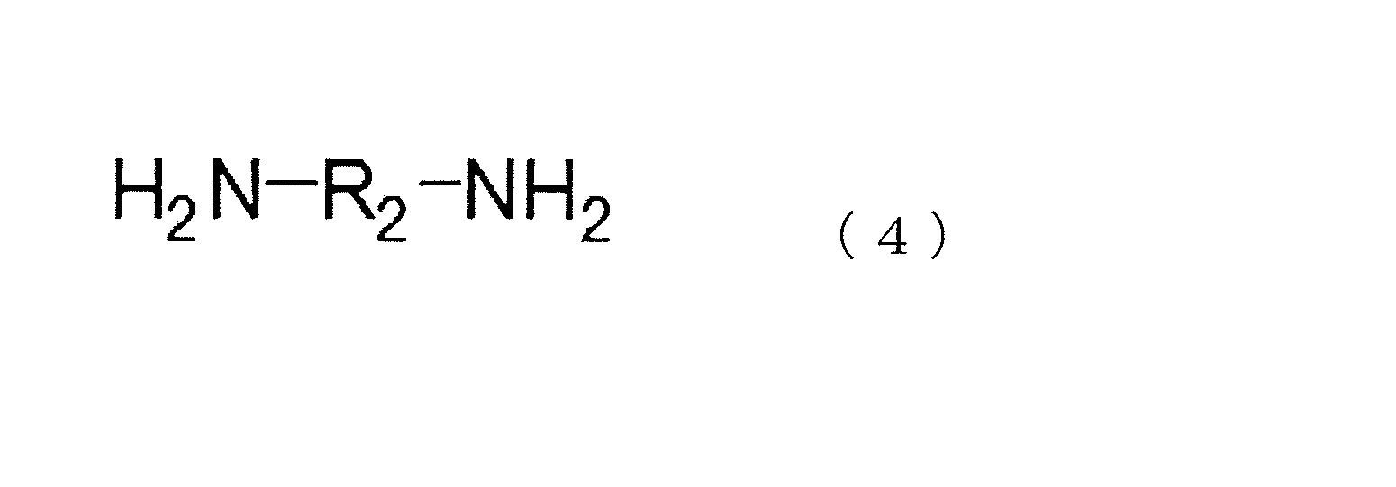
前記脂肪族鎖は、C、N、H、Oのいずれか一以上の原子からなる側鎖をさらに有してもよく、前記側鎖を構成する原子数の合計が10以下である)
アミン当量が4000~20000であるポリイミドを含む、半導体装置。 [20] A semiconductor chip, an electrode formed on the semiconductor chip, a sealing material for sealing the periphery of the semiconductor chip so that a part of the electrode is exposed, and formed on the sealing material A redistribution layer electrically connected to the electrode; an external connection electrode formed on the redistribution layer and electrically connected to the redistribution layer; the redistribution layer; and A polyimide layer disposed around an external connection electrode, and the polyimide layer includes a polycondensation unit of tetracarboxylic dianhydride (α) and diamine (β), and the tetracarboxylic dianhydride The product (α) includes an aromatic tetracarboxylic dianhydride (α1) having a benzophenone skeleton represented by the following formula (1), or the diamine (β) is represented by the following formula (2). Aromatic diamine having benzophenone skeleton (β ) Includes,
The aliphatic chain may further have a side chain composed of one or more atoms of C, N, H, and O, and the total number of atoms constituting the side chain is 10 or less)
A semiconductor device comprising a polyimide having an amine equivalent of 4000 to 20000.
後述の半導体基板の製造方法、および半導体装置の製造法に使用するポリイミドは、テトラカルボン酸二無水物(α)とジアミン(β)との重縮合ユニットを含む。そして、当該ポリイミドでは、テトラカルボン酸二無水物(α)が下記式(1)で表されるベンゾフェノン骨格を有する芳香族テトラカルボン酸二無水物(α1)を含むか、ジアミン(β)が下記式(2)で表されるベンゾフェノン骨格を有する芳香族ジアミン(β1)を含む。なお、ポリイミドは、芳香族テトラカルボン酸二無水物(α1)由来の構造、および芳香族ジアミン(β1)由来の構造の両方含んでいてもよい。


また、式(4-1)のp、qおよびrは、それぞれ独立に0~10の整数を示す。ただし、p+q+rは1以上であり、好ましくは5~20である。 In the formula (3-1), o represents an integer of 1 to 50, preferably an integer of 10 to 20.
In the formula (4-1), p, q and r each independently represent an integer of 0 to 10. However, p + q + r is 1 or more, preferably 5 to 20.
テトラカルボン酸二無水物(α)およびジアミン(β)の合計量に対する、芳香族テトラカルボン酸二無水物(α2)および芳香族ジアミン(β2)の合計量が40モル%以上95モル%以下であり、かつ
テトラカルボン酸二無水物(α)およびジアミン(β)の合計量に対する、ビフェニル骨格を有さず、ジフェニルエーテル骨格を有し、芳香環を3つ以上有する芳香族テトラカルボン酸二無水物(α3)、および、ビフェニル骨格を有さず、ジフェニルエーテル骨格を有し、芳香環を3つ以上有する芳香族ジアミン(β3)の合計量が、20モル%以上である。 Requirement c) The tetracarboxylic dianhydride (α) does not have a biphenyl skeleton and includes an aromatic tetracarboxylic dianhydride (α2) having a diphenyl ether skeleton, or the diamine (β) has a biphenyl skeleton. And an aromatic diamine (β2) having a diphenyl ether skeleton,
The total amount of aromatic tetracarboxylic dianhydride (α2) and aromatic diamine (β2) relative to the total amount of tetracarboxylic dianhydride (α) and diamine (β) is 40 mol% or more and 95 mol% or less. Aromatic tetracarboxylic dianhydride having no diphenyl ether skeleton, having a diphenyl ether skeleton, and having three or more aromatic rings, with respect to the total amount of tetracarboxylic dianhydride (α) and diamine (β) The total amount of (α3) and the aromatic diamine (β3) not having a biphenyl skeleton, having a diphenyl ether skeleton, and having three or more aromatic rings is 20 mol% or more.
要件e)粘度平均分子量ηが0.6以上1.60以下である。 Requirement d) The tetracarboxylic dianhydride (α) includes an aromatic tetracarboxylic dianhydride (α4) having a biphenyl skeleton, or the diamine (β) is an aromatic diamine (β4) having a biphenyl skeleton. And the total amount of aromatic tetracarboxylic dianhydride (α4) and aromatic diamine (β4) is 0 mol% or more and 45 mol% with respect to the total amount of tetracarboxylic dianhydride (α) and diamine (β) Is less than.
Requirement e) The viscosity average molecular weight η is 0.6 or more and 1.60 or less.
ポリイミドがテトラカルボン酸二無水物(α)およびジアミン(β)の合計量に対する、芳香族テトラカルボン酸二無水物(α1)および芳香族ジアミン(β1)の合計量が5モル%以上であると、上述のように、ポリイミドの耐熱性および溶媒への溶解性が高まりやすくなる。一方で、芳香族テトラカルボン酸二無水物(α1)および芳香族ジアミン(β1)の合計量が30モル%以下であると、ポリイミドの安定性が高まりやすくなる。 Regarding requirement a) The total amount of aromatic tetracarboxylic dianhydride (α1) and aromatic diamine (β1) is 5 mol% relative to the total amount of tetracarboxylic dianhydride (α) and diamine (β) of polyimide. When it is above, as described above, the heat resistance and solubility of the polyimide in the solvent are likely to increase. On the other hand, when the total amount of the aromatic tetracarboxylic dianhydride (α1) and the aromatic diamine (β1) is 30 mol% or less, the stability of the polyimide is likely to increase.
テトラカルボン酸二無水物(α)およびジアミン(β)の合計量に対する、主鎖に炭素数3以上の脂肪族鎖を有さないテトラカルボン酸二無水物およびジアミンの合計量が、95モル%以上であると、ポリイミドの耐熱性が非常に高くなる。なお、主鎖とは、ポリイミド分子の両末端の間に形成される、テトラカルボン酸二無水物(α)およびジアミン(β)の重縮合ユニットからなる構造をいい、側鎖を構成する原子を除いたものをいう。なお、側鎖には、炭素数3以上の脂肪族鎖が含まれていてもよいが、ポリイミドに非常に高い耐熱性が要求される場合には、側鎖にも炭素数3以上の脂肪族鎖を有さないことが好ましい。 Requirement b) The total amount of tetracarboxylic dianhydride and diamine having no aliphatic chain having 3 or more carbon atoms in the main chain with respect to the total amount of tetracarboxylic dianhydride (α) and diamine (β) is If it is 95 mol% or more, the heat resistance of the polyimide becomes very high. The main chain is a structure composed of polycondensation units of tetracarboxylic dianhydride (α) and diamine (β) formed between both ends of the polyimide molecule, and the atoms constituting the side chain are It means what was excluded. The side chain may contain an aliphatic chain having 3 or more carbon atoms, but if the polyimide requires very high heat resistance, the side chain also has an aliphatic chain having 3 or more carbon atoms. It is preferred not to have a chain.
テトラカルボン酸二無水物(α)が、ビフェニル骨格を有さず、ジフェニルエーテル骨格を有する芳香族テトラカルボン酸二無水物(α2)を含むか、ジアミン(β)が、ビフェニル骨格を有さず、ジフェニルエーテル骨格を有する芳香族ジアミン(β2)を含むと、ポリイミドの溶媒に対する溶解性が非常に高くなる。なお、芳香族ジアミン(β2)の一部は、上述の芳香族ジアミン(β1)に相当するものであってもよく、この場合、当該化合物は要件a)および要件c)の両方で考慮される。 Regarding Requirement c) The tetracarboxylic dianhydride (α) does not have a biphenyl skeleton and includes an aromatic tetracarboxylic dianhydride (α2) having a diphenyl ether skeleton, or the diamine (β) has a biphenyl skeleton. If the aromatic diamine (β2) having a diphenyl ether skeleton is included, the solubility of the polyimide in the solvent becomes very high. A part of the aromatic diamine (β2) may correspond to the above-mentioned aromatic diamine (β1), and in this case, the compound is considered in both the requirements a) and c). .
テトラカルボン酸二無水物(α)が、ビフェニル骨格を有する芳香族テトラカルボン酸二無水物(α4)を含むか、ジアミン(β)が、ビフェニル骨格を有する芳香族ジアミン(β4)を含み、テトラカルボン酸二無水物(α)およびジアミン(β)の合計量に対する、芳香族テトラカルボン酸二無水物(α4)および芳香族ジアミン(β4)の合計量が0モル%以上45モル%未満であると、ポリイミドの耐熱性が高まる。なお、芳香族ジアミン(β4)の一部は、上述の芳香族ジアミン(β1)に相当するものであってもよい。この場合、当該化合物は、要件a)および要件d)の両方で考慮される。 Regarding requirement d) The tetracarboxylic dianhydride (α) includes an aromatic tetracarboxylic dianhydride (α4) having a biphenyl skeleton, or the diamine (β) is an aromatic diamine (β4) having a biphenyl skeleton. The total amount of aromatic tetracarboxylic dianhydride (α4) and aromatic diamine (β4) is 0 mol% or more and 45 mol with respect to the total amount of tetracarboxylic dianhydride (α) and diamine (β) If it is less than%, the heat resistance of the polyimide increases. In addition, a part of aromatic diamine (β4) may correspond to the above-mentioned aromatic diamine (β1). In this case, the compound is considered in both requirement a) and requirement d).
ポリイミドの粘度平均分子量ηが、0.6以上であると、後述のポリイミド層の機械的強度が高まりやすくなる。一方、粘度平均分子量が、1.60以下であると、ポリイミドの溶媒への溶解性が高まる。なお、本明細書でいう粘度平均分子量ηは、以下の方法により算出した値とする。測定するポリイミドを三角フラスコに少量採取し、N-メチルピロリドン(NMP)を用いて0.5(g/dL)に希釈する。そして、調製した希釈ワニスについて、35℃恒温槽に入れたウベローテ管(柴田科学社製)で落下時間を測定する。そして、η=ln[希釈ワニス落下時間/NMP落下時間]より求めた値を粘度平均分子量ηとする。粘度平均分子量ηは、0.7以上であることがより好ましく、0.8以上であることがさらに好ましい。一方、ポリイミドの溶媒に対する溶解性の観点からは、粘度平均分子量ηは1.4以下であることがより好ましい。 Regarding requirement e) When the viscosity average molecular weight η of polyimide is 0.6 or more, the mechanical strength of the polyimide layer described later tends to increase. On the other hand, when the viscosity average molecular weight is 1.60 or less, the solubility of the polyimide in the solvent increases. The viscosity average molecular weight η referred to in this specification is a value calculated by the following method. A small amount of polyimide to be measured is collected in an Erlenmeyer flask and diluted to 0.5 (g / dL) with N-methylpyrrolidone (NMP). And about the prepared dilution varnish, fall time is measured with the Uberote tube (made by Shibata Kagaku company) put into the 35 degreeC thermostat. And let the value calculated | required from (eta) = ln [dilution varnish fall time / NMP fall time] be a viscosity average molecular weight (eta). The viscosity average molecular weight η is more preferably 0.7 or more, and further preferably 0.8 or more. On the other hand, from the viewpoint of solubility of the polyimide in the solvent, the viscosity average molecular weight η is more preferably 1.4 or less.
本発明の半導体基板の製造方法について説明する。前述のように、半導体基板の製造方法として、半導体ウエハの回路形成面側を支持材で支持しながら、半導体ウエハの回路非形成面を研削する手法が知られており、半導体ウエハと支持材とを貼り合わせるための接着層として、ポリイミドが知られている。従来の接着層(以下、「ポリイミド層」とも称する)は、ポリアミド酸を含むワニスを、支持材上に塗布することで形成されていた。しかしながら、このようなポリイミド層は、ポリアミド酸がイミド化する際に生じる水が層内に気泡として残留しやすい。そして、ポリイミド層が気泡を含むと、半導体ウエハの研削中に半導体ウエハが脱落したり、半導体ウエハの研削中に不均一に荷重が加わり、欠けや割れが生じる等の課題があった。 2. Manufacturing method of semiconductor substrate The manufacturing method of the semiconductor substrate of this invention is demonstrated. As described above, as a method for manufacturing a semiconductor substrate, there is known a method of grinding a circuit non-formation surface of a semiconductor wafer while supporting the circuit formation surface side of the semiconductor wafer with a support material. Polyimide is known as an adhesive layer for bonding together. Conventional adhesive layers (hereinafter also referred to as “polyimide layers”) are formed by applying a varnish containing polyamic acid onto a support material. However, in such a polyimide layer, water generated when the polyamic acid is imidized tends to remain as bubbles in the layer. When the polyimide layer contains air bubbles, there are problems such as dropping of the semiconductor wafer during grinding of the semiconductor wafer, non-uniform load during grinding of the semiconductor wafer, and chipping or cracking.
以下、本発明の半導体ウエハの製造方法における各工程について説明する。 Moreover, the manufacturing method of the semiconductor wafer of this invention may have processes other than the above, for example, the uneven | corrugated absorption layer which forms an uneven | corrugated absorption layer on a polyimide layer after a polyimide layer formation and before a wafer sticking process You may further have a wafer processing process etc. which process the circuit non-formation surface of a wafer after a formation process and a wafer grinding process.
Hereinafter, each process in the manufacturing method of the semiconductor wafer of this invention is demonstrated.
本発明のポリイミド層形成工程は、支持材上にポリイミド層を形成する工程である。
ポリイミド層を形成する支持材は、平滑な面を有し、かつ半導体ウエハの回路非形成面を研削する際に、半導体ウエハに撓み等を生じさせることなく支持可能な部材であれば特に制限されない。ここで、支持材の種類は、本工程におけるポリイミド層の形成方法や、後述の支持材剥離工程における支持材の剥離方法に応じて適宜選択される。例えば、本工程において、ポリイミドおよび溶媒を含むワニスを塗布し、ポリイミド層を形成する場合や、後述の支持材剥離工程において、ポリイミド層の一部を溶媒で溶解したりする場合には、これらの溶媒に対して十分な耐性を有する支持材が選択される。また、後述の支持材剥離工程において、支持材側からレーザ光を照射し、支持材を剥離する場合には、レーザ光の透過性が高い支持材が選択される。 2-1. Polyimide layer forming step The polyimide layer forming step of the present invention is a step of forming a polyimide layer on a support material.
The support material for forming the polyimide layer is not particularly limited as long as it is a member that has a smooth surface and can be supported without causing the semiconductor wafer to bend when the non-circuit-formed surface of the semiconductor wafer is ground. . Here, the kind of support material is suitably selected according to the formation method of the polyimide layer in this process, and the peeling method of the support material in the below-mentioned support material peeling process. For example, in this step, when a varnish containing polyimide and a solvent is applied to form a polyimide layer, or when a part of the polyimide layer is dissolved with a solvent in a support material peeling step described later, these A support material is selected that has sufficient resistance to the solvent. Moreover, in the support material peeling process mentioned later, when irradiating a laser beam from the support material side and peeling a support material, the support material with the high transmittance | permeability of a laser beam is selected.
上述のポリイミド層形成工程後、凹凸吸収層形成工程を行ってもよい。ポリイミド層上に凹凸吸収層を形成することで、支持材と貼り合わせる半導体ウエハの回路形成面の凹凸(例えば、電極、バンプ、半田ボール等による凹凸等)を吸収することができる。これにより、支持材と半導体ウエハとの密着性が高まり、半導体ウエハの研削中に半導体ウエハが脱落したり、局所的に荷重が加わって、半導体ウエハが割れたりすることを抑制することができる。 2-2. Concavity and convexity absorption layer formation process After the above-mentioned polyimide layer formation process, you may perform an unevenness | corrugation absorption layer formation process. By forming the uneven absorption layer on the polyimide layer, unevenness (for example, unevenness due to electrodes, bumps, solder balls, etc.) on the circuit forming surface of the semiconductor wafer to be bonded to the support material can be absorbed. Thereby, the adhesiveness between the support material and the semiconductor wafer is enhanced, and it is possible to suppress the semiconductor wafer from falling off during the grinding of the semiconductor wafer, or the semiconductor wafer from being cracked due to local load being applied.
また半導体ウエハに対する易貼り付け性、凹凸埋め込み性、易剥離性を向上させる目的で、公知の樹脂層をポリイミド層・凹凸吸収層上面にさらに形成しても構わない。 The thickness of the uneven absorption layer is preferably larger than the step provided on the circuit forming surface of the semiconductor wafer, and more preferably larger than the desired thickness of the semiconductor wafer (thickness of the semiconductor wafer after grinding). As a result, it becomes possible to perform a grinding process, which will be described later, in a state where most of the semiconductor wafer is embedded in the uneven absorption layer, and it is possible to suppress cracking and chipping at the edge of the semiconductor wafer.
A known resin layer may be further formed on the upper surface of the polyimide layer / concave-absorbing absorption layer for the purpose of improving easy pasting to the semiconductor wafer, uneven embedding property, and easy peelability.
続いて、支持材と半導体ウエハの回路形成面とを、前述のポリイミド層を介して貼り合わせる。なお、ポリイミド層上に凹凸吸収層を形成した場合、ポリイミド層および凹凸吸収層を介して支持材と半導体ウエハとを貼り合わせる。 2-3. Wafer pasting step Subsequently, the support material and the circuit forming surface of the semiconductor wafer are pasted together via the polyimide layer described above. In addition, when an uneven | corrugated absorption layer is formed on a polyimide layer, a support material and a semiconductor wafer are bonded together via a polyimide layer and an uneven | corrugated absorption layer.
支持材で回路形成面側を支持しながら、半導体ウエハの回路非形成面の研削を行う。半導体ウエハの研削方法は、公知の方法とすることができ、スルーフィード方式、インフィード方式のいずれの研削方式であってもよい。なお、いずれの方法においても、半導体ウエハと砥石との間に水を供給しながら、半導体ウエハが所望の厚みになるまで研削を行う。 2-4. Wafer grinding process The circuit non-formation surface of the semiconductor wafer is ground while supporting the circuit formation side with the support material. The semiconductor wafer may be ground by a known method, and may be either a through-feed method or an in-feed method. In either method, grinding is performed until the semiconductor wafer has a desired thickness while supplying water between the semiconductor wafer and the grindstone.
本発明の半導体基板の製造方法では、必要に応じて、半導体ウエハの回路非形成面を加工する工程を行ってもよく、回路非形成面を100℃以上の温度で加工してもよい。このような工程の一例として、銅やアルミニウム等の金属薄膜を回路非形成面に形成する工程(いわゆる、バックメタル工程)が挙げられる。 2-5. Wafer processing step In the method for manufacturing a semiconductor substrate of the present invention, if necessary, a step of processing a circuit non-formation surface of a semiconductor wafer may be performed, or even if a circuit non-formation surface is processed at a temperature of 100 ° C. or higher. Good. As an example of such a process, there is a process of forming a metal thin film such as copper or aluminum on a circuit non-formation surface (so-called back metal process).
支持材剥離工程では、ポリイミド層から支持材を剥離する。ポリイミド層から支持材を剥離する方法は、半導体ウエハの割れを防止するとの観点から、半導体ウエハに応力がかかり難い方法であることが好ましい。 2-6. Support material peeling process In a support material peeling process, a support material is peeled from a polyimide layer. The method of peeling the support material from the polyimide layer is preferably a method in which stress is not easily applied to the semiconductor wafer from the viewpoint of preventing cracking of the semiconductor wafer.
上記支持材剥離工程後、半導体ウエハの回路形成面からポリイミド層を剥離する。なお、ポリイミド層と半導体ウエハとの間に凹凸吸収層が介在する場合には、ポリイミド層と共に、凹凸吸収層も剥離することができる。 2-7. Polyimide layer peeling process After the said support material peeling process, a polyimide layer is peeled from the circuit formation surface of a semiconductor wafer. In addition, when an uneven | corrugated absorption layer interposes between a polyimide layer and a semiconductor wafer, an uneven | corrugated absorption layer can also be peeled with a polyimide layer.
次に、本発明の半導体装置の製造方法について説明する。前述のように、半導体装置の製造方法として、接着層を形成した支持材上に再配線層を形成し、当該再配線層上に半導体チップを実装することで、半導体装置を製造する方法が知られており、このような方法に用いる接着層として、ポリイミドが知られている。当該方法に用いられる接着層(以下「ポリイミド層」とも称する)も、通常、ポリアミド酸を含むワニスを、支持材上に塗布することで形成されていた。前述のように、このようなポリイミド層では、ポリアミド酸がイミド化する際に生じる水が層内に気泡として残留しやすい。そして、半導体装置の製造方法では、再配線層を形成したり、半導体チップを実装したり、半導体チップを封止する工程が必要であり、これらの工程では、ポリイミド層や支持材に熱がかかる。そのため、ポリイミド層が気泡を含むと、これらの工程で気泡が膨張し、再配線層にクラックが生じたり、再配線層が剥離したりしやすくなる。 3. Next, a method for manufacturing a semiconductor device of the present invention will be described. As described above, as a method of manufacturing a semiconductor device, a method of manufacturing a semiconductor device by forming a rewiring layer on a support material on which an adhesive layer is formed and mounting a semiconductor chip on the rewiring layer is known. Polyimide is known as an adhesive layer used in such a method. The adhesive layer (hereinafter also referred to as “polyimide layer”) used in the method is usually formed by applying a varnish containing polyamic acid on a support material. As described above, in such a polyimide layer, water generated when the polyamic acid is imidized tends to remain as bubbles in the layer. And in the manufacturing method of a semiconductor device, the process of forming a rewiring layer, mounting a semiconductor chip, or sealing a semiconductor chip is required, and heat is applied to a polyimide layer and a support material in these processes. . Therefore, when the polyimide layer contains bubbles, the bubbles expand in these steps, and the rewiring layer is easily cracked or the rewiring layer is easily peeled off.
以下、本発明の半導体装置の製造方法における各工程について説明する。 Moreover, the manufacturing method of the semiconductor device of this invention may have processes other than the above, for example, a peeling layer is formed on the polyimide layer after the polyimide layer forming process and before the rewiring layer forming process. You may have the peeling layer formation process to do. In addition, after the support material peeling step, the peeling layer peeling step for peeling the peeling layer, the external connection electrode forming step for forming the external connection electrode electrically connected to the rewiring layer, and the semiconductor device are separated. You may have a process etc.
Hereafter, each process in the manufacturing method of the semiconductor device of this invention is demonstrated.
本発明の半導体装置の製造方法におけるポリイミド層形成工程は、支持材上にポリイミド層を形成する工程である。ポリイミド層を形成する支持材は、平滑な面を有し、半導体装置の製造の際に、撓むことなく、再配線層等を支持可能な部材であれば特に制限されない。支持材の種類は、本工程におけるポリイミド層の形成方法や、後述の支持材剥離工程における支持材の剥離方法に応じて適宜選択される。例えば、本工程において、ポリイミドおよび溶媒を含むワニスを塗布し、ポリイミド層を形成する場合や、後述の支持材剥離工程において、ポリイミド層の一部を溶媒で溶解したりする場合には、これらの溶媒に対して十分な耐性を有する支持材が選択される。また、後述の支持材剥離工程において、支持材側からレーザ光を照射し、支持材を剥離する場合には、レーザ光の透過性が高い支持材が選択される。このような支持材としては、上述の半導体基板の製造方法に用いる支持材と同様とすることができ、その形状や厚みは、所望の半導体装置の大きさや種類等に合わせて適宜選択される。 3-1. Polyimide layer formation process The polyimide layer formation process in the manufacturing method of the semiconductor device of this invention is a process of forming a polyimide layer on a support material. The support material for forming the polyimide layer is not particularly limited as long as it is a member that has a smooth surface and can support the rewiring layer and the like without bending when the semiconductor device is manufactured. The kind of the support material is appropriately selected according to the method for forming the polyimide layer in this step and the method for peeling the support material in the support material peeling step described later. For example, in this step, when a varnish containing polyimide and a solvent is applied to form a polyimide layer, or when a part of the polyimide layer is dissolved with a solvent in a support material peeling step described later, these A support material is selected that has sufficient resistance to the solvent. Moreover, in the support material peeling process mentioned later, when irradiating a laser beam from the support material side and peeling a support material, the support material with the high laser beam permeability | transmittance is selected. Such a support material can be the same as the support material used in the above-described method for manufacturing a semiconductor substrate, and the shape and thickness thereof are appropriately selected according to the size and type of a desired semiconductor device.
上述のポリイミド層形成工程もしくは剥離層形成工程後、剥離層形成工程を行ってもよい。剥離層を形成した場合、後述の剥離層剥離工程によって、再配線層上からポリイミド層を容易に除去することが可能となる。 3-2. Release layer forming step After the polyimide layer forming step or the release layer forming step, the release layer forming step may be performed. When the release layer is formed, the polyimide layer can be easily removed from the rewiring layer by a later-described release layer peeling step.
続いて、上記ポリイミド層(剥離層形成工程を行った場合には、剥離層)上に再配線層を形成する。再配線層は、導通路やその周囲に配置される絶縁樹脂等からなる層とすることができる。ここで、本発明の方法によれば、支持材上に多くの半導体装置を一度に形成することが可能である。本工程では、再配線層を1つのみ形成してもよく、2つ以上形成してもよい。また、異なる配線パターンを有する再配線層を形成してもよい。 3-3. Rewiring layer forming step Subsequently, a rewiring layer is formed on the polyimide layer (or a peeling layer when the peeling layer forming step is performed). The rewiring layer can be a layer made of an insulating resin or the like disposed around the conduction path. Here, according to the method of the present invention, it is possible to form many semiconductor devices on the support material at a time. In this step, only one rewiring layer may be formed, or two or more rewiring layers may be formed. Further, a rewiring layer having a different wiring pattern may be formed.
その後、再配線層上に半導体チップを配置し、再配線層と半導体チップとを電気的に接続する。具体的には、再配線層の導通路上に、半導体チップの電極が位置するように配置し、これらが電気的に導通するよう、フリップチップボンディング等により接合する。なお、支持材上に複数の再配線層が形成されている場合には、各再配線層上に、それぞれ半導体チップを接合する。再配線層と接合する半導体チップの種類や大きさ等は特に制限されず、所望の半導体装置に合わせて適宜選択される。 3-4. Semiconductor chip bonding step Thereafter, a semiconductor chip is disposed on the rewiring layer, and the rewiring layer and the semiconductor chip are electrically connected. Specifically, the electrodes of the semiconductor chip are arranged on the conduction path of the rewiring layer, and are joined by flip chip bonding or the like so that they are electrically conducted. When a plurality of rewiring layers are formed on the support material, a semiconductor chip is bonded to each rewiring layer. The type and size of the semiconductor chip bonded to the redistribution layer is not particularly limited, and is appropriately selected according to a desired semiconductor device.
半導体チップの実装後、半導体チップの再配線層との接続部以外の部分を、封止材にて封止する。半導体チップの封止方法は、公知の方法とすることができる。例えば、エポキシ樹脂等の硬化性樹脂および充填材を含む樹脂組成物を半導体チップ上にディスペンサーによって塗布したり、各種印刷法で印刷する。その後、樹脂組成物を硬化させることにより、封止材を形成することができる。 3-5. Sealing Step After mounting the semiconductor chip, a portion other than the connection portion with the rewiring layer of the semiconductor chip is sealed with a sealing material. The semiconductor chip sealing method may be a known method. For example, a resin composition containing a curable resin such as an epoxy resin and a filler is applied onto a semiconductor chip by a dispenser or printed by various printing methods. Then, a sealing material can be formed by hardening a resin composition.
続いて、ポリイミド層から支持材を剥離する。ポリイミド層から支持材を剥離する方法は、再配線層のクラックや断線を防止するとの観点から、再配線層や半導体チップ等に応力がかかり難い方法であることが好ましい。 3-6. Support material peeling process Then, a support material is peeled from a polyimide layer. The method of peeling the support material from the polyimide layer is preferably a method in which stress is not easily applied to the rewiring layer, the semiconductor chip, and the like from the viewpoint of preventing cracking and disconnection of the rewiring layer.
上述の剥離層形成工程で剥離層を形成した場合には、支持材の剥離後、剥離層およびポリイミド層を剥離する工程を行ってもよい。 3-7. Peeling layer peeling process When a peeling layer is formed in the above-mentioned peeling layer forming process, you may perform the process of peeling a peeling layer and a polyimide layer after peeling of a support material.
また、必要に応じて、再配線層上に外部接続用電極を形成する工程を行ってもよい。なお、ポリイミド層が再配線層上に残存している場合には、ポリイミド層の一部をレーザー加工やリソグラフィー加工などでパターニングすることで、再配線層と電気的に外部接続用電極とを電気的に接続することが可能となる。このようにポリイミド層を外部接続用電極の周囲に残存させると、外部接続用電極(半田ボール)の割れ等が抑制されるとの利点がある。 3-8. External Connection Electrode Forming Step If necessary, a step of forming an external connection electrode on the rewiring layer may be performed. When the polyimide layer remains on the rewiring layer, a part of the polyimide layer is patterned by laser processing or lithography processing to electrically connect the rewiring layer and the external connection electrode. Can be connected to each other. Thus, when the polyimide layer is left around the external connection electrode, there is an advantage that cracking of the external connection electrode (solder ball) is suppressed.
上述のように、本発明の半導体装置の製造方法によれば、複数の半導体装置を支持材上で一度に形成することが可能である。そこで、上述の支持材剥離工程後、任意のタイミングで、半導体装置を個片化する工程を行ってもよい。個片化方法は特に制限されず、公知の方法とすることができる。 3-9. As described above, according to the method for manufacturing a semiconductor device of the present invention, a plurality of semiconductor devices can be formed on a support material at a time. Therefore, after the above support material peeling step, a step of dividing the semiconductor device into individual pieces may be performed at an arbitrary timing. The singulation method is not particularly limited, and can be a known method.
三井化学株式会社製ポリイミドワニスMP14C(ガラス転移温度138℃のポリイミドを、NMPに0.1質量%以上溶解させたワニス、粘度2,000mPas)を使用した。 (Polyimide varnish)
A polyimide varnish MP14C manufactured by Mitsui Chemicals, Inc. (a varnish obtained by dissolving 0.1% by mass or more of a polyimide having a glass transition temperature of 138 ° C. in NMP at a viscosity of 2,000 mPas) was used.
前記ポリイミドワニスを、ガラス基材上にスピンコーター(1000mPs、-10sec)にて塗膜した。ガラス基板上に形成されたポリイミド塗布液は窒素雰囲気で満たし150℃に設定した乾燥機中に10分間投入して乾燥した。ガラス基板上に貼り付けられた厚み20μmのポリイミドフィルムを得た。 (
The polyimide varnish was coated on a glass substrate with a spin coater (1000 mPs, −10 sec). The polyimide coating solution formed on the glass substrate was filled in a nitrogen atmosphere and dried for 10 minutes in a dryer set at 150 ° C. A polyimide film having a thickness of 20 μm stuck on a glass substrate was obtained.
あらかじめラミネートシート(PET基材)上に前記ポリイミドワニスを用いて形成した厚み20μmのポリイミドフィルムを、200℃に加熱したガラス基材に圧着してポリイミドフィルムを固着したのち、ラミネートシートを剥離し、ガラス基板の上面に貼り付けられたポリイミドフィルムを形成した。 (
A polyimide film having a thickness of 20 μm formed in advance on the laminate sheet (PET base material) using the polyimide varnish was pressed onto a glass base material heated to 200 ° C. to fix the polyimide film, and then the laminate sheet was peeled off. A polyimide film attached to the upper surface of the glass substrate was formed.
ガラス基板の表面に前記貼り付け方法1および方法2にてポリイミドフィルムを形成し、ガラスとポリイミドフィルムの積層体を得た。この積層体を用いガラス基板の裏面側(フィルム積層面と反対側)から、選択的に355nmの固体UVレーザービーム(出力85W、剥離エネルギー密度は210mJ/cm2、ビームサイズは100×0.035mm、バルス幅60ns)を照射した。
貼り付け方法1および方法2にて得たそれぞれの積層体につき、レーザーアブレーション効果により、ポリイミド層はガラス界面から剥がれることを確認した。 [Example 1]
A polyimide film was formed on the surface of the glass substrate by the attaching
About each laminated body obtained by the
2、12 ポリイミド層
3 半導体ウエハ
3’ 半導体基板
3a 回路形成面
3b 回路非形成面
13 再配線層
14 半導体チップ
15 封止材
16 外部接続用電極
17 電極
100 半導体装置
DESCRIPTION OF
Claims (21)
- 支持材上にポリイミド層を形成するポリイミド層形成工程と、
前記支持材と、半導体ウエハの回路形成面とを、前記ポリイミド層を介して貼り合わせるウエハ貼付工程と、
前記支持材が貼り付けられた前記半導体ウエハの回路非形成面を研削するウエハ研削工程と、
前記ポリイミド層から前記支持材を剥離する支持材剥離工程と、
前記半導体ウエハから前記ポリイミド層を剥離するポリイミド層剥離工程と、を含み、
前記ポリイミド層に用いられるポリイミドが210℃以下のガラス転移温度を有し、かつ溶媒に溶解する、半導体基板の製造方法。 A polyimide layer forming step of forming a polyimide layer on the support material;
A wafer pasting step of pasting the support and the circuit forming surface of the semiconductor wafer through the polyimide layer;
A wafer grinding step of grinding a non-circuit-formed surface of the semiconductor wafer to which the support material is attached;
A support material peeling step of peeling the support material from the polyimide layer;
A polyimide layer peeling step for peeling the polyimide layer from the semiconductor wafer,
The manufacturing method of a semiconductor substrate with which the polyimide used for the said polyimide layer has a glass transition temperature of 210 degrees C or less, and melt | dissolves in a solvent. - 前記ポリイミドが、
テトラカルボン酸二無水物(α)とジアミン(β)との重縮合ユニットを含み、
前記テトラカルボン酸二無水物(α)が、下記式(1)で表されるベンゾフェノン骨格を有する芳香族テトラカルボン酸二無水物(α1)を含むか、前記ジアミン(β)が、下記式(2)で表されるベンゾフェノン骨格を有する芳香族ジアミン(β1)を含み、


A polycondensation unit of tetracarboxylic dianhydride (α) and diamine (β),
The tetracarboxylic dianhydride (α) includes an aromatic tetracarboxylic dianhydride (α1) having a benzophenone skeleton represented by the following formula (1), or the diamine (β) is represented by the following formula ( 2) an aromatic diamine (β1) having a benzophenone skeleton represented by
- 前記ジアミン(β)が、下記式(3)または(4)で表される脂肪族ジアミン(β5)を含み、

前記脂肪族鎖は、C、N、H、Oのいずれか一以上の原子からなる側鎖をさらに有してもよく、前記側鎖を構成する原子数の合計が10以下である)

前記脂肪族鎖は、C、N、H、Oのいずれか一以上の原子からなる側鎖をさらに有してもよく、前記側鎖を構成する原子数の合計が10以下である)
前記ポリイミドのアミン当量が4000~20000である、
請求項2に記載の半導体基板の製造方法。 The diamine (β) includes an aliphatic diamine (β5) represented by the following formula (3) or (4),
The aliphatic chain may further have a side chain composed of one or more atoms of C, N, H, and O, and the total number of atoms constituting the side chain is 10 or less)
The aliphatic chain may further have a side chain composed of one or more atoms of C, N, H, and O, and the total number of atoms constituting the side chain is 10 or less)
The amine equivalent of the polyimide is 4000-20000,
A method for manufacturing a semiconductor substrate according to claim 2. - 前記テトラカルボン酸二無水物(α)および前記ジアミン(β)の合計量に対する、前記芳香族テトラカルボン酸二無水物(α1)および前記芳香族ジアミン(β1)の合計量が5~30モル%であり、
前記テトラカルボン酸二無水物(α)および前記ジアミン(β)の合計量に対する、主鎖に炭素数3以上の脂肪族鎖を有さないテトラカルボン酸二無水物およびジアミンの合計量が、95モル%以上であり、
前記テトラカルボン酸二無水物(α)が、ビフェニル骨格を有さず、ジフェニルエーテル骨格を有する芳香族テトラカルボン酸二無水物(α2)を含むか、前記ジアミン(β)が、ビフェニル骨格を有さず、ジフェニルエーテル骨格を有する芳香族ジアミン(β2)を含み、
前記テトラカルボン酸二無水物(α)および前記ジアミン(β)の合計量に対する、前記芳香族テトラカルボン酸二無水物(α2)および前記芳香族ジアミン(β2)の合計量が40モル%以上95モル%以下であり、かつ前記テトラカルボン酸二無水物(α)および前記ジアミン(β)の合計量に対する、ビフェニル骨格を有さず、ジフェニルエーテル骨格を有し、芳香環を3つ以上有する芳香族テトラカルボン酸二無水物(α3)、および、ビフェニル骨格を有さず、ジフェニルエーテル骨格を有し、芳香環を3つ以上有する芳香族ジアミン(β3)の合計量が、20モル%以上であり、
前記テトラカルボン酸二無水物(α)が、ビフェニル骨格を有する芳香族テトラカルボン酸二無水物(α4)を含むか、前記ジアミン(β)が、ビフェニル骨格を有する芳香族ジアミン(β4)を含み、
前記テトラカルボン酸二無水物(α)および前記ジアミン(β)の合計量に対する、前記芳香族テトラカルボン酸二無水物(α4)および前記芳香族ジアミン(β4)の合計量が0モル%以上45モル%未満であり、
前記ポリイミドの粘度平均分子量ηが0.6以上1.60以下である、
請求項3に記載の半導体基板の製造方法。 The total amount of the aromatic tetracarboxylic dianhydride (α1) and the aromatic diamine (β1) is 5 to 30 mol% based on the total amount of the tetracarboxylic dianhydride (α) and the diamine (β). And
The total amount of tetracarboxylic dianhydride and diamine having no aliphatic chain having 3 or more carbon atoms in the main chain is 95 with respect to the total amount of tetracarboxylic dianhydride (α) and diamine (β). Mol% or more,
The tetracarboxylic dianhydride (α) does not have a biphenyl skeleton and includes an aromatic tetracarboxylic dianhydride (α2) having a diphenyl ether skeleton, or the diamine (β) has a biphenyl skeleton. And an aromatic diamine (β2) having a diphenyl ether skeleton,
The total amount of the aromatic tetracarboxylic dianhydride (α2) and the aromatic diamine (β2) with respect to the total amount of the tetracarboxylic dianhydride (α) and the diamine (β) is 40 mol% or more and 95 Aromatics having no more than mol% and having no diphenyl ether skeleton, no diphenyl ether skeleton, and three or more aromatic rings with respect to the total amount of the tetracarboxylic dianhydride (α) and the diamine (β). The total amount of tetracarboxylic dianhydride (α3) and aromatic diamine (β3) having no diphenyl ether skeleton and three or more aromatic rings, having no biphenyl skeleton, is 20 mol% or more,
The tetracarboxylic dianhydride (α) includes an aromatic tetracarboxylic dianhydride (α4) having a biphenyl skeleton, or the diamine (β) includes an aromatic diamine (β4) having a biphenyl skeleton. ,
The total amount of the aromatic tetracarboxylic dianhydride (α4) and the aromatic diamine (β4) with respect to the total amount of the tetracarboxylic dianhydride (α) and the diamine (β) is 0 mol% or more and 45 Less than mol%,
The viscosity average molecular weight η of the polyimide is 0.6 or more and 1.60 or less,
A method for manufacturing a semiconductor substrate according to claim 3. - 前記ウエハ研削工程後、前記支持材剥離工程前に、前記半導体ウエハの回路非形成面を、180℃以上の温度で加工するウエハ加工工程をさらに有する、
請求項1~4のいずれかに記載の半導体基板の製造方法。 After the wafer grinding step, before the support material peeling step, further comprising a wafer processing step of processing the circuit non-formed surface of the semiconductor wafer at a temperature of 180 ° C. or higher.
The method for producing a semiconductor substrate according to any one of claims 1 to 4. - 前記ポリイミド層形成工程後、前記ウエハ貼付工程前に、前記ポリイミド層上に凹凸吸収層を形成する凹凸吸収層形成工程をさらに有し、
前記ウエハ貼付工程が、前記ポリイミド層および前記凹凸吸収層を介して、前記支持材と前記半導体ウエハの回路形成面とを貼り合わせる工程であり、
前記ポリイミド層剥離工程が、前記半導体ウエハから前記凹凸吸収層および前記ポリイミド層を剥離する工程である、
請求項1~5のいずれか一項に記載の半導体基板の製造方法。 After the polyimide layer forming step, before the wafer pasting step, further comprising an uneven absorption layer forming step of forming an uneven absorption layer on the polyimide layer,
The wafer pasting step is a step of pasting the support material and the circuit forming surface of the semiconductor wafer through the polyimide layer and the uneven absorption layer,
The polyimide layer peeling step is a step of peeling the uneven absorption layer and the polyimide layer from the semiconductor wafer.
The method for producing a semiconductor substrate according to any one of claims 1 to 5. - 前記支持材剥離工程が、前記支持材と前記ポリイミド層との界面にレーザ光を照射する工程である、
請求項1~6のいずれか一項に記載の半導体基板の製造方法。 The support material peeling step is a step of irradiating a laser beam to an interface between the support material and the polyimide layer.
The method for manufacturing a semiconductor substrate according to any one of claims 1 to 6. - 前記支持材剥離工程が、前記ポリイミド層の少なくとも一部を溶媒で溶解させる工程である、
請求項1~6のいずれか一項に記載の半導体基板の製造方法。 The support material peeling step is a step of dissolving at least a part of the polyimide layer with a solvent.
The method for manufacturing a semiconductor substrate according to any one of claims 1 to 6. - 前記ポリイミド層形成工程が、溶媒および前記ポリイミドを含むワニスを塗布し、前記ワニスを乾燥させる工程である、
請求項1~8のいずれか一項に記載の半導体基板の製造方法。 The polyimide layer forming step is a step of applying a solvent and a varnish containing the polyimide, and drying the varnish.
The method for producing a semiconductor substrate according to any one of claims 1 to 8. - 前記ポリイミド層形成工程が、前記ポリイミドを含むポリイミドシートを、前記支持材に貼り付ける工程である、
請求項1~8のいずれか一項に記載の半導体基板の製造方法。 The polyimide layer forming step is a step of attaching a polyimide sheet containing the polyimide to the support material.
The method for producing a semiconductor substrate according to any one of claims 1 to 8. - 支持材上にポリイミド層を形成するポリイミド層形成工程と、
前記ポリイミド層を介して前記支持材上に再配線層を形成する再配線層形成工程と、
前記再配線層上に、半導体チップを配置し、前記再配線層と前記半導体チップとを電気的に導通するよう、接合させる半導体チップ接合工程と、
前記再配線層と接合された前記半導体チップを封止材で封止する封止工程と、
前記支持材を前記ポリイミド層から剥離する支持材剥離工程と、
を含み、
前記ポリイミド層に用いられるポリイミドが、210℃以下のガラス転移温度を有し、かつ溶媒に溶解する、半導体装置の製造方法。 A polyimide layer forming step of forming a polyimide layer on the support material;
A rewiring layer forming step of forming a rewiring layer on the support material via the polyimide layer;
A semiconductor chip bonding step of disposing a semiconductor chip on the rewiring layer and bonding the rewiring layer and the semiconductor chip so as to be electrically connected;
A sealing step of sealing the semiconductor chip bonded to the rewiring layer with a sealing material;
A support material peeling step of peeling the support material from the polyimide layer;
Including
A method for manufacturing a semiconductor device, wherein a polyimide used for the polyimide layer has a glass transition temperature of 210 ° C. or lower and is dissolved in a solvent. - 前記ポリイミドが、
テトラカルボン酸二無水物(α)とジアミン(β)との重縮合ユニットを含み、
前記テトラカルボン酸二無水物(α)が、下記式(1)で表されるベンゾフェノン骨格を有する芳香族テトラカルボン酸二無水物(α1)を含むか、前記ジアミン(β)が、下記式(2)で表されるベンゾフェノン骨格を有する芳香族ジアミン(β1)を含み、


前記ジアミン(β)が、下記式(3)または(4)で表される脂肪族ジアミン(β5)を含み、

前記脂肪族鎖は、C、N、H、Oのいずれか一以上の原子からなる側鎖をさらに有してもよく、前記側鎖を構成する原子数の合計が10以下である)

前記脂肪族鎖は、C、N、H、Oのいずれか一以上の原子からなる側鎖をさらに有してもよく、前記側鎖を構成する原子数の合計が10以下である)
前記ポリイミドのアミン当量が4000~20000である、請求項11に記載の半導体装置の製造方法。 The polyimide is
A polycondensation unit of tetracarboxylic dianhydride (α) and diamine (β),
The tetracarboxylic dianhydride (α) includes an aromatic tetracarboxylic dianhydride (α1) having a benzophenone skeleton represented by the following formula (1), or the diamine (β) is represented by the following formula ( 2) an aromatic diamine (β1) having a benzophenone skeleton represented by
The diamine (β) includes an aliphatic diamine (β5) represented by the following formula (3) or (4),
The aliphatic chain may further have a side chain composed of one or more atoms of C, N, H, and O, and the total number of atoms constituting the side chain is 10 or less)
The aliphatic chain may further have a side chain composed of one or more atoms of C, N, H, and O, and the total number of atoms constituting the side chain is 10 or less)
The method of manufacturing a semiconductor device according to claim 11, wherein the amine equivalent of the polyimide is 4000 to 20000. - 前記テトラカルボン酸二無水物(α)および前記ジアミン(β)の合計量に対する、前記芳香族テトラカルボン酸二無水物(α1)および前記芳香族ジアミン(β1)の合計量が5~30モル%であり、
前記テトラカルボン酸二無水物(α)および前記ジアミン(β)の合計量に対する、主鎖に炭素数3以上の脂肪族鎖を有さないテトラカルボン酸二無水物およびジアミンの合計量が、95モル%以上であり、
前記テトラカルボン酸二無水物(α)が、ビフェニル骨格を有さず、ジフェニルエーテル骨格を有する芳香族テトラカルボン酸二無水物(α2)を含むか、前記ジアミン(β)が、ビフェニル骨格を有さず、ジフェニルエーテル骨格を有する芳香族ジアミン(β2)を含み、
前記テトラカルボン酸二無水物(α)および前記ジアミン(β)の合計量に対する、前記芳香族テトラカルボン酸二無水物(α2)および前記芳香族ジアミン(β2)の合計量が40モル%以上95モル%以下であり、かつ前記テトラカルボン酸二無水物(α)および前記ジアミン(β)の合計量に対する、ビフェニル骨格を有さず、ジフェニルエーテル骨格を有し、芳香環を3つ以上有する芳香族テトラカルボン酸二無水物(α3)、および、ビフェニル骨格を有さず、ジフェニルエーテル骨格を有し、芳香環を3つ以上有する芳香族ジアミン(β3)の合計量が、20モル%以上であり、
前記テトラカルボン酸二無水物(α)が、ビフェニル骨格を有する芳香族テトラカルボン酸二無水物(α4)を含むか、前記ジアミン(β)が、ビフェニル骨格を有する芳香族ジアミン(β4)を含み、
前記テトラカルボン酸二無水物(α)および前記ジアミン(β)の合計量に対する、前記芳香族テトラカルボン酸二無水物(α4)および前記芳香族ジアミン(β4)の合計量が0モル%以上45モル%未満であり、
前記ポリイミドの粘度平均分子量ηが0.6以上1.60以下である、
請求項12に記載の半導体装置の製造方法。 The total amount of the aromatic tetracarboxylic dianhydride (α1) and the aromatic diamine (β1) is 5 to 30 mol% based on the total amount of the tetracarboxylic dianhydride (α) and the diamine (β). And
The total amount of tetracarboxylic dianhydride and diamine having no aliphatic chain having 3 or more carbon atoms in the main chain is 95 with respect to the total amount of tetracarboxylic dianhydride (α) and diamine (β). Mol% or more,
The tetracarboxylic dianhydride (α) does not have a biphenyl skeleton and includes an aromatic tetracarboxylic dianhydride (α2) having a diphenyl ether skeleton, or the diamine (β) has a biphenyl skeleton. And an aromatic diamine (β2) having a diphenyl ether skeleton,
The total amount of the aromatic tetracarboxylic dianhydride (α2) and the aromatic diamine (β2) with respect to the total amount of the tetracarboxylic dianhydride (α) and the diamine (β) is 40 mol% or more and 95 Aromatics having no more than mol% and having no diphenyl ether skeleton, no diphenyl ether skeleton, and three or more aromatic rings with respect to the total amount of the tetracarboxylic dianhydride (α) and the diamine (β). The total amount of tetracarboxylic dianhydride (α3) and aromatic diamine (β3) having no diphenyl ether skeleton and three or more aromatic rings, having no biphenyl skeleton, is 20 mol% or more,
The tetracarboxylic dianhydride (α) includes an aromatic tetracarboxylic dianhydride (α4) having a biphenyl skeleton, or the diamine (β) includes an aromatic diamine (β4) having a biphenyl skeleton. ,
The total amount of the aromatic tetracarboxylic dianhydride (α4) and the aromatic diamine (β4) with respect to the total amount of the tetracarboxylic dianhydride (α) and the diamine (β) is 0 mol% or more and 45 Less than mol%,
The viscosity average molecular weight η of the polyimide is 0.6 or more and 1.60 or less,
A method for manufacturing a semiconductor device according to claim 12. - 前記ポリイミド層形成工程後、前記再配線層形成工程前に、前記ポリイミド層上に剥離層を形成する剥離層形成工程をさらに有し、
前記再配線層形成工程が、前記ポリイミド層および前記剥離層を介して、前記支持材上に前記再配線層を形成する工程であり、
前記支持材剥離工程後、前記再配線層から前記剥離層を剥離する剥離層剥離工程をさらに有する、
請求項11~13のいずれか一項に記載の半導体装置の製造方法。 After the polyimide layer forming step, before the rewiring layer forming step, further comprising a peeling layer forming step of forming a peeling layer on the polyimide layer,
The rewiring layer forming step is a step of forming the rewiring layer on the support material via the polyimide layer and the release layer,
After the support material peeling step, further comprising a peeling layer peeling step for peeling the peeling layer from the rewiring layer,
The method for manufacturing a semiconductor device according to any one of claims 11 to 13. - 前記支持材剥離工程後、前記再配線層上に、前記再配線層と電気的に接続する外部接続用電極を形成する外部接続用電極形成工程をさらに有する、
請求項11~14のいずれか一項に記載の半導体装置の製造方法。 After the supporting material peeling step, further comprising an external connection electrode forming step for forming an external connection electrode electrically connected to the rewiring layer on the rewiring layer.
The method for manufacturing a semiconductor device according to any one of claims 11 to 14. - 前記支持材剥離工程が、前記支持材と前記ポリイミド層との界面にレーザを照射する工程である、
請求項11~15のいずれか一項に記載の半導体装置の製造方法。 The support material peeling step is a step of irradiating a laser to the interface between the support material and the polyimide layer.
The method for manufacturing a semiconductor device according to any one of claims 11 to 15. - 前記支持材剥離工程が、前記ポリイミド層の少なくとも一部を溶媒で溶解させる工程である、
請求項11~15のいずれか一項に記載の半導体装置の製造方法。 The support material peeling step is a step of dissolving at least a part of the polyimide layer with a solvent.
The method for manufacturing a semiconductor device according to any one of claims 11 to 15. - 前記ポリイミド層形成工程が、溶媒および前記ポリイミドを含むワニスを塗布し、前記ワニスを乾燥させる工程である、
請求項11~17のいずれか一項に記載の半導体装置の製造方法。 The polyimide layer forming step is a step of applying a solvent and a varnish containing the polyimide, and drying the varnish.
The method for manufacturing a semiconductor device according to any one of claims 11 to 17. - 前記ポリイミド層形成工程が、前記ポリイミドを含むポリイミドシートを、前記支持材に貼り付ける工程である、
請求項11~17のいずれか一項に記載の半導体装置の製造方法。 The polyimide layer forming step is a step of attaching a polyimide sheet containing the polyimide to the support material.
The method for manufacturing a semiconductor device according to any one of claims 11 to 17. - 半導体チップと、
前記半導体チップ上に形成された電極と、
前記電極の一部が露出するように、前記半導体チップの周囲を封止する封止材と、
前記封止材上に形成され、前記電極と電気的に接続された再配線層と、
前記再配線層上に形成され、前記再配線層と電気的に接続された外部接続用電極と、
前記再配線層上、かつ前記外部接続用電極の周囲に配置されたポリイミド層と、
を含み、
前記ポリイミド層が、
テトラカルボン酸二無水物(α)とジアミン(β)との重縮合ユニットを含み、
前記テトラカルボン酸二無水物(α)が、下記式(1)で表されるベンゾフェノン骨格を有する芳香族テトラカルボン酸二無水物(α1)を含むか、前記ジアミン(β)が、下記式(2)で表されるベンゾフェノン骨格を有する芳香族ジアミン(β1)を含み、


前記ジアミン(β)が、下記式(3)または(4)で表される脂肪族ジアミン(β5)を含み、

前記脂肪族鎖は、C、N、H、Oのいずれか一以上の原子からなる側鎖をさらに有してもよく、前記側鎖を構成する原子数の合計が10以下である)

前記脂肪族鎖は、C、N、H、Oのいずれか一以上の原子からなる側鎖をさらに有してもよく、前記側鎖を構成する原子数の合計が10以下である)
アミン当量が4000~20000であるポリイミドを含む、半導体装置。 A semiconductor chip;
An electrode formed on the semiconductor chip;
A sealing material for sealing the periphery of the semiconductor chip so that a part of the electrode is exposed;
A rewiring layer formed on the sealing material and electrically connected to the electrode;
An external connection electrode formed on the rewiring layer and electrically connected to the rewiring layer;
A polyimide layer disposed on the rewiring layer and around the external connection electrode;
Including
The polyimide layer is
A polycondensation unit of tetracarboxylic dianhydride (α) and diamine (β),
The tetracarboxylic dianhydride (α) includes an aromatic tetracarboxylic dianhydride (α1) having a benzophenone skeleton represented by the following formula (1), or the diamine (β) is represented by the following formula ( 2) an aromatic diamine (β1) having a benzophenone skeleton represented by
The diamine (β) includes an aliphatic diamine (β5) represented by the following formula (3) or (4),
The aliphatic chain may further have a side chain composed of one or more atoms of C, N, H, and O, and the total number of atoms constituting the side chain is 10 or less)
The aliphatic chain may further have a side chain composed of one or more atoms of C, N, H, and O, and the total number of atoms constituting the side chain is 10 or less)
A semiconductor device comprising a polyimide having an amine equivalent of 4000 to 20000. - 前記ポリイミドが、
前記テトラカルボン酸二無水物(α)および前記ジアミン(β)の合計量に対する、前記芳香族テトラカルボン酸二無水物(α1)および前記芳香族ジアミン(β1)の合計量が5~30モル%であり、
前記テトラカルボン酸二無水物(α)および前記ジアミン(β)の合計量に対する、主鎖に炭素数3以上の脂肪族鎖を有さないテトラカルボン酸二無水物およびジアミンの合計量が、95モル%以上であり、
前記テトラカルボン酸二無水物(α)が、ビフェニル骨格を有さず、ジフェニルエーテル骨格を有する芳香族テトラカルボン酸二無水物(α2)を含むか、前記ジアミン(β)が、ビフェニル骨格を有さず、ジフェニルエーテル骨格を有する芳香族ジアミン(β2)を含み、
前記テトラカルボン酸二無水物(α)および前記ジアミン(β)の合計量に対する、前記芳香族テトラカルボン酸二無水物(α2)および前記芳香族ジアミン(β2)の合計量が40モル%以上95モル%以下であり、かつ前記テトラカルボン酸二無水物(α)および前記ジアミン(β)の合計量に対する、ビフェニル骨格を有さず、ジフェニルエーテル骨格を有し、芳香環を3つ以上有する芳香族テトラカルボン酸二無水物(α3)、および、ビフェニル骨格を有さず、ジフェニルエーテル骨格を有し、芳香環を3つ以上有する芳香族ジアミン(β3)の合計量が、20モル%以上であり、
前記テトラカルボン酸二無水物(α)が、ビフェニル骨格を有する芳香族テトラカルボン酸二無水物(α4)を含むか、前記ジアミン(β)が、ビフェニル骨格を有する芳香族ジアミン(β4)を含み、
前記テトラカルボン酸二無水物(α)および前記ジアミン(β)の合計量に対する、前記芳香族テトラカルボン酸二無水物(α4)および前記芳香族ジアミン(β4)の合計量が0モル%以上45モル%未満であり、
粘度平均分子量ηが0.6以上1.60以下である、
請求項20に記載の半導体装置。
The polyimide is
The total amount of the aromatic tetracarboxylic dianhydride (α1) and the aromatic diamine (β1) is 5 to 30 mol% based on the total amount of the tetracarboxylic dianhydride (α) and the diamine (β). And
The total amount of tetracarboxylic dianhydride and diamine having no aliphatic chain having 3 or more carbon atoms in the main chain is 95 with respect to the total amount of tetracarboxylic dianhydride (α) and diamine (β). Mol% or more,
The tetracarboxylic dianhydride (α) does not have a biphenyl skeleton and includes an aromatic tetracarboxylic dianhydride (α2) having a diphenyl ether skeleton, or the diamine (β) has a biphenyl skeleton. And an aromatic diamine (β2) having a diphenyl ether skeleton,
The total amount of the aromatic tetracarboxylic dianhydride (α2) and the aromatic diamine (β2) with respect to the total amount of the tetracarboxylic dianhydride (α) and the diamine (β) is 40 mol% or more and 95 Aromatics having no more than mol% and having no diphenyl ether skeleton, no diphenyl ether skeleton, and three or more aromatic rings with respect to the total amount of the tetracarboxylic dianhydride (α) and the diamine (β). The total amount of tetracarboxylic dianhydride (α3) and aromatic diamine (β3) having no diphenyl ether skeleton and three or more aromatic rings, having no biphenyl skeleton, is 20 mol% or more,
The tetracarboxylic dianhydride (α) includes an aromatic tetracarboxylic dianhydride (α4) having a biphenyl skeleton, or the diamine (β) includes an aromatic diamine (β4) having a biphenyl skeleton. ,
The total amount of the aromatic tetracarboxylic dianhydride (α4) and the aromatic diamine (β4) with respect to the total amount of the tetracarboxylic dianhydride (α) and the diamine (β) is 0 mol% or more and 45 Less than mol%,
The viscosity average molecular weight η is 0.6 or more and 1.60 or less,
The semiconductor device according to claim 20.
Priority Applications (5)
| Application Number | Priority Date | Filing Date | Title |
|---|---|---|---|
| US16/606,789 US10988647B2 (en) | 2017-04-21 | 2018-04-19 | Semiconductor substrate manufacturing method, semiconductor device, and method for manufacturing same |
| SG11201909822T SG11201909822TA (en) | 2017-04-21 | 2018-04-19 | Semiconductor substrate manufacturing method, semiconductor device, and method for manufacturing same |
| JP2019513685A JP6963602B2 (en) | 2017-04-21 | 2018-04-19 | Semiconductor substrate manufacturing method |
| CN201880025788.8A CN110546746A (en) | 2017-04-21 | 2018-04-19 | method for manufacturing semiconductor substrate, semiconductor device and method for manufacturing the same |
| KR1020197030753A KR102442262B1 (en) | 2017-04-21 | 2018-04-19 | A method for manufacturing a semiconductor substrate, a semiconductor device, and a method for manufacturing the same |
Applications Claiming Priority (2)
| Application Number | Priority Date | Filing Date | Title |
|---|---|---|---|
| JP2017-084694 | 2017-04-21 | ||
| JP2017084694 | 2017-04-21 |
Publications (1)
| Publication Number | Publication Date |
|---|---|
| WO2018194133A1 true WO2018194133A1 (en) | 2018-10-25 |
Family
ID=63856146
Family Applications (1)
| Application Number | Title | Priority Date | Filing Date |
|---|---|---|---|
| PCT/JP2018/016187 WO2018194133A1 (en) | 2017-04-21 | 2018-04-19 | Semiconductor substrate manufacturing method, semiconductor device, and method for manufacturing same |
Country Status (7)
| Country | Link |
|---|---|
| US (1) | US10988647B2 (en) |
| JP (1) | JP6963602B2 (en) |
| KR (1) | KR102442262B1 (en) |
| CN (1) | CN110546746A (en) |
| SG (1) | SG11201909822TA (en) |
| TW (1) | TWI816670B (en) |
| WO (1) | WO2018194133A1 (en) |
Cited By (1)
| Publication number | Priority date | Publication date | Assignee | Title |
|---|---|---|---|---|
| JP7451780B2 (en) | 2022-01-20 | 2024-03-18 | 東友ファインケム株式会社 | Polyimide precursor composition, polyimide film formed from it, and method for manufacturing semiconductor devices using the same |
Families Citing this family (1)
| Publication number | Priority date | Publication date | Assignee | Title |
|---|---|---|---|---|
| US11973058B2 (en) | 2021-11-25 | 2024-04-30 | International Business Machines Corporation | Multiple die assembly |
Citations (10)
| Publication number | Priority date | Publication date | Assignee | Title |
|---|---|---|---|---|
| JP2005116610A (en) * | 2003-10-03 | 2005-04-28 | Nitto Denko Corp | Processing method of semiconductor wafer, and adhesive sheet for processing semiconductor wafer |
| WO2013008437A1 (en) * | 2011-07-08 | 2013-01-17 | 三井化学株式会社 | Polyimide resin composition and laminate including same |
| WO2013099173A1 (en) * | 2011-12-26 | 2013-07-04 | 三井化学株式会社 | Multilayer molded body and method for producing same, electromagnetic shield member, and heat-dissipating member |
| WO2013183293A1 (en) * | 2012-06-07 | 2013-12-12 | 三井化学株式会社 | Polyimide resin composition, film, adhesive agent and component |
| WO2014003056A1 (en) * | 2012-06-29 | 2014-01-03 | 日立化成株式会社 | Method for producing semiconductor device |
| WO2014196296A1 (en) * | 2013-06-07 | 2014-12-11 | 日東電工株式会社 | Method for manufacturing semiconductor device |
| WO2015033867A1 (en) * | 2013-09-09 | 2015-03-12 | 日東電工株式会社 | Method for manufacturing semiconductor device |
| WO2015053132A1 (en) * | 2013-10-07 | 2015-04-16 | 東レ株式会社 | Element-processing layered structure, method for manufacturing element-processing layered structure, and method for manufacturing thin element using same |
| JP2016056060A (en) * | 2014-09-10 | 2016-04-21 | 株式会社オハラ | substrate |
| JP2016219511A (en) * | 2015-05-15 | 2016-12-22 | 日立化成株式会社 | Resin composition for temporary fixation, resin film for temporary fixation, and resin film sheet for temporary fixation |
Family Cites Families (8)
| Publication number | Priority date | Publication date | Assignee | Title |
|---|---|---|---|---|
| US20100193950A1 (en) * | 2009-01-30 | 2010-08-05 | E.I.Du Pont De Nemours And Company | Wafer level, chip scale semiconductor device packaging compositions, and methods relating thereto |
| JP2011132354A (en) * | 2009-12-24 | 2011-07-07 | Hitachi Maxell Ltd | Ultraviolet-curing adhesive film |
| US8643165B2 (en) * | 2011-02-23 | 2014-02-04 | Texas Instruments Incorporated | Semiconductor device having agglomerate terminals |
| TWI440412B (en) | 2011-12-28 | 2014-06-01 | Princo Corp | Package method of thin multi-layer substrate |
| US9895868B2 (en) * | 2012-06-20 | 2018-02-20 | Toyobo Co., Ltd. | Method for producing layered product, layered product, method for producing layered product with device using said layered product, and layered product with device |
| CN105683319A (en) * | 2013-10-30 | 2016-06-15 | 琳得科株式会社 | Semiconductor bonding adhesive sheet and semiconductor device manufacturing method |
| SG11201700478YA (en) * | 2014-07-22 | 2017-02-27 | Brewer Science Inc | Polyimides as laser release materials for 3-d ic applications |
| US20160133486A1 (en) * | 2014-11-07 | 2016-05-12 | International Business Machines Corporation | Double Layer Release Temporary Bond and Debond Processes and Systems |
-
2018
- 2018-04-19 WO PCT/JP2018/016187 patent/WO2018194133A1/en active Application Filing
- 2018-04-19 SG SG11201909822T patent/SG11201909822TA/en unknown
- 2018-04-19 JP JP2019513685A patent/JP6963602B2/en active Active
- 2018-04-19 US US16/606,789 patent/US10988647B2/en active Active
- 2018-04-19 CN CN201880025788.8A patent/CN110546746A/en active Pending
- 2018-04-19 KR KR1020197030753A patent/KR102442262B1/en active IP Right Grant
- 2018-04-20 TW TW107113572A patent/TWI816670B/en active
Patent Citations (10)
| Publication number | Priority date | Publication date | Assignee | Title |
|---|---|---|---|---|
| JP2005116610A (en) * | 2003-10-03 | 2005-04-28 | Nitto Denko Corp | Processing method of semiconductor wafer, and adhesive sheet for processing semiconductor wafer |
| WO2013008437A1 (en) * | 2011-07-08 | 2013-01-17 | 三井化学株式会社 | Polyimide resin composition and laminate including same |
| WO2013099173A1 (en) * | 2011-12-26 | 2013-07-04 | 三井化学株式会社 | Multilayer molded body and method for producing same, electromagnetic shield member, and heat-dissipating member |
| WO2013183293A1 (en) * | 2012-06-07 | 2013-12-12 | 三井化学株式会社 | Polyimide resin composition, film, adhesive agent and component |
| WO2014003056A1 (en) * | 2012-06-29 | 2014-01-03 | 日立化成株式会社 | Method for producing semiconductor device |
| WO2014196296A1 (en) * | 2013-06-07 | 2014-12-11 | 日東電工株式会社 | Method for manufacturing semiconductor device |
| WO2015033867A1 (en) * | 2013-09-09 | 2015-03-12 | 日東電工株式会社 | Method for manufacturing semiconductor device |
| WO2015053132A1 (en) * | 2013-10-07 | 2015-04-16 | 東レ株式会社 | Element-processing layered structure, method for manufacturing element-processing layered structure, and method for manufacturing thin element using same |
| JP2016056060A (en) * | 2014-09-10 | 2016-04-21 | 株式会社オハラ | substrate |
| JP2016219511A (en) * | 2015-05-15 | 2016-12-22 | 日立化成株式会社 | Resin composition for temporary fixation, resin film for temporary fixation, and resin film sheet for temporary fixation |
Cited By (1)
| Publication number | Priority date | Publication date | Assignee | Title |
|---|---|---|---|---|
| JP7451780B2 (en) | 2022-01-20 | 2024-03-18 | 東友ファインケム株式会社 | Polyimide precursor composition, polyimide film formed from it, and method for manufacturing semiconductor devices using the same |
Also Published As
| Publication number | Publication date |
|---|---|
| US20200377772A1 (en) | 2020-12-03 |
| JP6963602B2 (en) | 2021-11-10 |
| KR20190123793A (en) | 2019-11-01 |
| US10988647B2 (en) | 2021-04-27 |
| SG11201909822TA (en) | 2019-11-28 |
| TWI816670B (en) | 2023-10-01 |
| TW201900829A (en) | 2019-01-01 |
| CN110546746A (en) | 2019-12-06 |
| JPWO2018194133A1 (en) | 2020-02-27 |
| KR102442262B1 (en) | 2022-09-08 |
Similar Documents
| Publication | Publication Date | Title |
|---|---|---|
| TWI797066B (en) | Temporary bonding method using laminate film for temporary bonding, and method of manufacturing semiconductor device using the same | |
| TWI278471B (en) | Adhesive polyimide resin and adhesive laminate | |
| KR102260081B1 (en) | Adhesive for temporary bonding, adhesive layer, method for manufacturing wafer work piece and semiconductor device using same, polyimide copolymer, polyimide mixed resin, and resin composition | |
| TW201906896A (en) | Curable polyimine | |
| TWI615422B (en) | Resin composition, cured film, laminated film, and method of manufacturing semiconductor device | |
| TWI652286B (en) | Polyimine resin composition and laminated film, and manufacturing method of semiconductor device | |
| CN108603028B (en) | Resin composition, resin layer, temporary adhesive, laminated film, wafer processed body, and application thereof | |
| TW201609402A (en) | Polyimides as laser release materials for 3-D IC applications | |
| TW201012893A (en) | Dual side adhesive film and electric part using the same | |
| JP6435862B2 (en) | LAMINATE FOR ELEMENT PROCESSING, METHOD FOR PRODUCING LAMINATE FOR ELEMENT PROCESSING, AND METHOD FOR PRODUCING THIN ELEMENT USING THE SAME | |
| TW202106761A (en) | Phenolic functionalized polyimides and compositions thereof | |
| WO2018194133A1 (en) | Semiconductor substrate manufacturing method, semiconductor device, and method for manufacturing same | |
| JP2017141317A (en) | Temporarily stuck resin composition, resin layer, permanent adhesive, temporarily stuck adhesive, wafer processed body, and method for manufacturing semiconductor device using them | |
| TW202306779A (en) | Laminate and manufacturing method of semiconductor device | |
| WO2014083973A1 (en) | Semiconductor-device manufacturing method | |
| JP7183840B2 (en) | Adhesive composition for temporary attachment and method for producing semiconductor electronic component using the same | |
| TWI694508B (en) | Adhesive tape for semiconductor processing | |
| TWI836502B (en) | Application of laser-releasable composition | |
| TW202402549A (en) | Application of laser-releasable composition | |
| TW202239903A (en) | Laminate, resin composition, and method for manufacturing semiconductor device |
Legal Events
| Date | Code | Title | Description |
|---|---|---|---|
| 121 | Ep: the epo has been informed by wipo that ep was designated in this application |
Ref document number: 18788331 Country of ref document: EP Kind code of ref document: A1 |
|
| ENP | Entry into the national phase |
Ref document number: 2019513685 Country of ref document: JP Kind code of ref document: A |
|
| ENP | Entry into the national phase |
Ref document number: 20197030753 Country of ref document: KR Kind code of ref document: A |
|
| NENP | Non-entry into the national phase |
Ref country code: DE |
|
| 122 | Ep: pct application non-entry in european phase |
Ref document number: 18788331 Country of ref document: EP Kind code of ref document: A1 |