WO2018096767A1 - Electronic control apparatus, in-vehicle system, and power supply control method - Google Patents
Electronic control apparatus, in-vehicle system, and power supply control method Download PDFInfo
- Publication number
- WO2018096767A1 WO2018096767A1 PCT/JP2017/032772 JP2017032772W WO2018096767A1 WO 2018096767 A1 WO2018096767 A1 WO 2018096767A1 JP 2017032772 W JP2017032772 W JP 2017032772W WO 2018096767 A1 WO2018096767 A1 WO 2018096767A1
- Authority
- WO
- WIPO (PCT)
- Prior art keywords
- circuit
- power supply
- power
- control
- control unit
- Prior art date
Links
Images


Classifications
-
- B—PERFORMING OPERATIONS; TRANSPORTING
- B60—VEHICLES IN GENERAL
- B60W—CONJOINT CONTROL OF VEHICLE SUB-UNITS OF DIFFERENT TYPE OR DIFFERENT FUNCTION; CONTROL SYSTEMS SPECIALLY ADAPTED FOR HYBRID VEHICLES; ROAD VEHICLE DRIVE CONTROL SYSTEMS FOR PURPOSES NOT RELATED TO THE CONTROL OF A PARTICULAR SUB-UNIT
- B60W50/00—Details of control systems for road vehicle drive control not related to the control of a particular sub-unit, e.g. process diagnostic or vehicle driver interfaces
- B60W50/06—Improving the dynamic response of the control system, e.g. improving the speed of regulation or avoiding hunting or overshoot
-
- B—PERFORMING OPERATIONS; TRANSPORTING
- B60—VEHICLES IN GENERAL
- B60R—VEHICLES, VEHICLE FITTINGS, OR VEHICLE PARTS, NOT OTHERWISE PROVIDED FOR
- B60R16/00—Electric or fluid circuits specially adapted for vehicles and not otherwise provided for; Arrangement of elements of electric or fluid circuits specially adapted for vehicles and not otherwise provided for
- B60R16/02—Electric or fluid circuits specially adapted for vehicles and not otherwise provided for; Arrangement of elements of electric or fluid circuits specially adapted for vehicles and not otherwise provided for electric constitutive elements
-
- B—PERFORMING OPERATIONS; TRANSPORTING
- B60—VEHICLES IN GENERAL
- B60W—CONJOINT CONTROL OF VEHICLE SUB-UNITS OF DIFFERENT TYPE OR DIFFERENT FUNCTION; CONTROL SYSTEMS SPECIALLY ADAPTED FOR HYBRID VEHICLES; ROAD VEHICLE DRIVE CONTROL SYSTEMS FOR PURPOSES NOT RELATED TO THE CONTROL OF A PARTICULAR SUB-UNIT
- B60W30/00—Purposes of road vehicle drive control systems not related to the control of a particular sub-unit, e.g. of systems using conjoint control of vehicle sub-units, or advanced driver assistance systems for ensuring comfort, stability and safety or drive control systems for propelling or retarding the vehicle
- B60W30/18—Propelling the vehicle
- B60W30/182—Selecting between different operative modes, e.g. comfort and performance modes
-
- B—PERFORMING OPERATIONS; TRANSPORTING
- B60—VEHICLES IN GENERAL
- B60W—CONJOINT CONTROL OF VEHICLE SUB-UNITS OF DIFFERENT TYPE OR DIFFERENT FUNCTION; CONTROL SYSTEMS SPECIALLY ADAPTED FOR HYBRID VEHICLES; ROAD VEHICLE DRIVE CONTROL SYSTEMS FOR PURPOSES NOT RELATED TO THE CONTROL OF A PARTICULAR SUB-UNIT
- B60W50/00—Details of control systems for road vehicle drive control not related to the control of a particular sub-unit, e.g. process diagnostic or vehicle driver interfaces
- B60W50/04—Monitoring the functioning of the control system
-
- F—MECHANICAL ENGINEERING; LIGHTING; HEATING; WEAPONS; BLASTING
- F02—COMBUSTION ENGINES; HOT-GAS OR COMBUSTION-PRODUCT ENGINE PLANTS
- F02D—CONTROLLING COMBUSTION ENGINES
- F02D45/00—Electrical control not provided for in groups F02D41/00 - F02D43/00
-
- G—PHYSICS
- G05—CONTROLLING; REGULATING
- G05F—SYSTEMS FOR REGULATING ELECTRIC OR MAGNETIC VARIABLES
- G05F1/00—Automatic systems in which deviations of an electric quantity from one or more predetermined values are detected at the output of the system and fed back to a device within the system to restore the detected quantity to its predetermined value or values, i.e. retroactive systems
- G05F1/10—Regulating voltage or current
- G05F1/46—Regulating voltage or current wherein the variable actually regulated by the final control device is dc
-
- G—PHYSICS
- G06—COMPUTING; CALCULATING OR COUNTING
- G06F—ELECTRIC DIGITAL DATA PROCESSING
- G06F1/00—Details not covered by groups G06F3/00 - G06F13/00 and G06F21/00
- G06F1/26—Power supply means, e.g. regulation thereof
-
- H—ELECTRICITY
- H02—GENERATION; CONVERSION OR DISTRIBUTION OF ELECTRIC POWER
- H02M—APPARATUS FOR CONVERSION BETWEEN AC AND AC, BETWEEN AC AND DC, OR BETWEEN DC AND DC, AND FOR USE WITH MAINS OR SIMILAR POWER SUPPLY SYSTEMS; CONVERSION OF DC OR AC INPUT POWER INTO SURGE OUTPUT POWER; CONTROL OR REGULATION THEREOF
- H02M3/00—Conversion of dc power input into dc power output
- H02M3/02—Conversion of dc power input into dc power output without intermediate conversion into ac
- H02M3/04—Conversion of dc power input into dc power output without intermediate conversion into ac by static converters
- H02M3/10—Conversion of dc power input into dc power output without intermediate conversion into ac by static converters using discharge tubes with control electrode or semiconductor devices with control electrode
- H02M3/145—Conversion of dc power input into dc power output without intermediate conversion into ac by static converters using discharge tubes with control electrode or semiconductor devices with control electrode using devices of a triode or transistor type requiring continuous application of a control signal
- H02M3/155—Conversion of dc power input into dc power output without intermediate conversion into ac by static converters using discharge tubes with control electrode or semiconductor devices with control electrode using devices of a triode or transistor type requiring continuous application of a control signal using semiconductor devices only
-
- H—ELECTRICITY
- H02—GENERATION; CONVERSION OR DISTRIBUTION OF ELECTRIC POWER
- H02M—APPARATUS FOR CONVERSION BETWEEN AC AND AC, BETWEEN AC AND DC, OR BETWEEN DC AND DC, AND FOR USE WITH MAINS OR SIMILAR POWER SUPPLY SYSTEMS; CONVERSION OF DC OR AC INPUT POWER INTO SURGE OUTPUT POWER; CONTROL OR REGULATION THEREOF
- H02M1/00—Details of apparatus for conversion
- H02M1/0003—Details of control, feedback or regulation circuits
- H02M1/0016—Control circuits providing compensation of output voltage deviations using feedforward of disturbance parameters
- H02M1/0019—Control circuits providing compensation of output voltage deviations using feedforward of disturbance parameters the disturbance parameters being load current fluctuations
-
- H—ELECTRICITY
- H02—GENERATION; CONVERSION OR DISTRIBUTION OF ELECTRIC POWER
- H02M—APPARATUS FOR CONVERSION BETWEEN AC AND AC, BETWEEN AC AND DC, OR BETWEEN DC AND DC, AND FOR USE WITH MAINS OR SIMILAR POWER SUPPLY SYSTEMS; CONVERSION OF DC OR AC INPUT POWER INTO SURGE OUTPUT POWER; CONTROL OR REGULATION THEREOF
- H02M1/00—Details of apparatus for conversion
- H02M1/0003—Details of control, feedback or regulation circuits
- H02M1/0025—Arrangements for modifying reference values, feedback values or error values in the control loop of a converter
-
- H—ELECTRICITY
- H02—GENERATION; CONVERSION OR DISTRIBUTION OF ELECTRIC POWER
- H02M—APPARATUS FOR CONVERSION BETWEEN AC AND AC, BETWEEN AC AND DC, OR BETWEEN DC AND DC, AND FOR USE WITH MAINS OR SIMILAR POWER SUPPLY SYSTEMS; CONVERSION OF DC OR AC INPUT POWER INTO SURGE OUTPUT POWER; CONTROL OR REGULATION THEREOF
- H02M3/00—Conversion of dc power input into dc power output
- H02M3/02—Conversion of dc power input into dc power output without intermediate conversion into ac
- H02M3/04—Conversion of dc power input into dc power output without intermediate conversion into ac by static converters
- H02M3/10—Conversion of dc power input into dc power output without intermediate conversion into ac by static converters using discharge tubes with control electrode or semiconductor devices with control electrode
- H02M3/145—Conversion of dc power input into dc power output without intermediate conversion into ac by static converters using discharge tubes with control electrode or semiconductor devices with control electrode using devices of a triode or transistor type requiring continuous application of a control signal
- H02M3/155—Conversion of dc power input into dc power output without intermediate conversion into ac by static converters using discharge tubes with control electrode or semiconductor devices with control electrode using devices of a triode or transistor type requiring continuous application of a control signal using semiconductor devices only
- H02M3/156—Conversion of dc power input into dc power output without intermediate conversion into ac by static converters using discharge tubes with control electrode or semiconductor devices with control electrode using devices of a triode or transistor type requiring continuous application of a control signal using semiconductor devices only with automatic control of output voltage or current, e.g. switching regulators
- H02M3/1566—Conversion of dc power input into dc power output without intermediate conversion into ac by static converters using discharge tubes with control electrode or semiconductor devices with control electrode using devices of a triode or transistor type requiring continuous application of a control signal using semiconductor devices only with automatic control of output voltage or current, e.g. switching regulators with means for compensating against rapid load changes, e.g. with auxiliary current source, with dual mode control or with inductance variation
-
- H—ELECTRICITY
- H02—GENERATION; CONVERSION OR DISTRIBUTION OF ELECTRIC POWER
- H02M—APPARATUS FOR CONVERSION BETWEEN AC AND AC, BETWEEN AC AND DC, OR BETWEEN DC AND DC, AND FOR USE WITH MAINS OR SIMILAR POWER SUPPLY SYSTEMS; CONVERSION OF DC OR AC INPUT POWER INTO SURGE OUTPUT POWER; CONTROL OR REGULATION THEREOF
- H02M3/00—Conversion of dc power input into dc power output
- H02M3/02—Conversion of dc power input into dc power output without intermediate conversion into ac
- H02M3/04—Conversion of dc power input into dc power output without intermediate conversion into ac by static converters
- H02M3/10—Conversion of dc power input into dc power output without intermediate conversion into ac by static converters using discharge tubes with control electrode or semiconductor devices with control electrode
- H02M3/145—Conversion of dc power input into dc power output without intermediate conversion into ac by static converters using discharge tubes with control electrode or semiconductor devices with control electrode using devices of a triode or transistor type requiring continuous application of a control signal
- H02M3/155—Conversion of dc power input into dc power output without intermediate conversion into ac by static converters using discharge tubes with control electrode or semiconductor devices with control electrode using devices of a triode or transistor type requiring continuous application of a control signal using semiconductor devices only
- H02M3/156—Conversion of dc power input into dc power output without intermediate conversion into ac by static converters using discharge tubes with control electrode or semiconductor devices with control electrode using devices of a triode or transistor type requiring continuous application of a control signal using semiconductor devices only with automatic control of output voltage or current, e.g. switching regulators
- H02M3/158—Conversion of dc power input into dc power output without intermediate conversion into ac by static converters using discharge tubes with control electrode or semiconductor devices with control electrode using devices of a triode or transistor type requiring continuous application of a control signal using semiconductor devices only with automatic control of output voltage or current, e.g. switching regulators including plural semiconductor devices as final control devices for a single load
Definitions
- the present invention relates to an electronic control device, an in-vehicle system, and a power supply control method, and more particularly to a technique effective for controlling a power supply that supplies power to a logic circuit whose circuit configuration can be changed.
- Autonomous driving is a system that can solve various social issues such as reducing the number of accidents and eliminating traffic jams.
- an automatic driving system it is necessary to detect a vehicle, a pedestrian, a white line, and the like from sensor inputs such as a camera and a radar, and transmit them to the driver, or control a brake and a steering. Therefore, advanced recognition algorithms and simultaneous processing of a plurality of algorithms are required.
- the FPGA is a reconfigurable circuit that can change the logic circuit, and has a feature that it is possible to perform processing provided in a plurality of hardware on one circuit.
- a logic circuit but also an electronic circuit in general can be used only when power is supplied from a power supply circuit.
- the load state of at least one circuit block is determined as a function of an enable signal or a clock signal, and the output current of the power supply apparatus is determined as the load state of at least one circuit block.
- the power supply device controls the output current (see, for example, Patent Document 1).
- the output voltage transiently decreases and increases as the load current increases and decreases rapidly.
- a power supply circuit that supplies current to the FPGA is required to have a function of constantly supplying a constant voltage even when there is a sudden load fluctuation.
- An object of the present invention is to provide a technique capable of reducing a transient increase / decrease in power supplied to a logic circuit whose circuit configuration can be changed.
- a typical electronic control device has a reconfiguration circuit, a function control unit, a power supply circuit, and a power supply control unit.
- the reconfigurable circuit is a reconfigurable logic circuit.
- the function control unit determines the operation mode of the reconfiguration circuit based on the mode determination signal indicating the operation mode of the vehicle, and controls the reconfiguration of the reconfiguration circuit based on the determination result.
- the power supply circuit supplies a power supply voltage to the reconstruction circuit.
- the power control unit controls the power circuit.
- the power supply control unit controls the load current generated by the power supply circuit before the load change of the reconfiguration circuit based on the power supply control information that is information for controlling the power supply circuit.
- the power supply control information includes the operation mode of the reconfiguration circuit and the control information in the power supply circuit corresponding to the operation mode.
- the power supply control unit acquires control information corresponding to the operation mode determined by the function control unit from the power supply control information.
- the power control unit searches the power control information stored in the power control database for control information corresponding to the operation mode determined by the function control unit.
- a transient increase or decrease in the output voltage of the power supply circuit that supplies power to the reconfiguration circuit, which is a logic circuit whose circuit configuration can be changed, can be reduced.
- FIG. 1 is a block diagram illustrating an example of a configuration of an in-vehicle system according to Embodiment 1.
- FIG. It is a block diagram which shows an example of a structure in autonomous running control ECU which the vehicle-mounted system of FIG. 1 has. It is explanatory drawing of the mode database which the autonomous running control logic part of FIG. 2 has. It is explanatory drawing of the process item database which the autonomous running control logic part of FIG. 2 has. It is explanatory drawing of the power supply control database which the autonomous running control logic part of FIG. 2 has. It is a flowchart which shows an example of the power supply control process in the power supply control part of FIG. It is a sequence diagram which shows an example of the power supply control process in the power supply control part of FIG.
- the constituent elements are not necessarily indispensable unless otherwise specified and apparently essential in principle. Needless to say.
- the autonomous traveling control ECU 201 includes a reconfiguration circuit 209 that is a reconfigurable logic circuit, a function control unit 207 that controls reconfiguration of the reconfiguration circuit 209, and a reconfiguration circuit.
- a power supply circuit 211 that supplies a power supply voltage to 209 and a power supply control unit 206 that controls the power supply circuit 211 are included.
- the autonomous traveling control ECU 201 has a power control database 212 in which power control information corresponding to each operation ID that is a plurality of processes from the function control unit 207 to the reconfiguration circuit 209 or a rewrite between a plurality of processes is stored. .
- the power control unit 206 extracts power control information from the power control database 212 based on the calculation ID received from the function control unit 207. Based on the extracted power supply control information, the power supply circuit 211 that supplies the power supply voltage to the reconfiguration circuit 209 is controlled.
- FIG. 1 is a block diagram showing an example of the configuration of an in-vehicle system according to the first embodiment.
- the in-vehicle system 10 is a system that controls the autonomous traveling of the vehicle, for example.
- the in-vehicle system 10 includes a camera 101, a radar 102, a vehicle position sensor 103, an automatic operation button 104, a wireless communication device 105, an auxiliary control ECU 106, a brake control ECU (Electronic Control Unit). 107, an engine control ECU 108, a power steering control ECU 109, and an autonomous travel control ECU 201.
- the camera 101, the radar 102, and the own vehicle position sensor 103 are external recognition sensors that recognize the external environment of the vehicle.
- the camera 101 and the radar 102 are sensors for recognizing the outside world and obtaining a distance to an object.
- the own vehicle position sensor 103 is a sensor that detects the own vehicle position by GPS (Global Positioning System) or the like.
- the automatic operation button 104 is a button for starting automatic operation control or changing the automatic operation mode.
- the wireless communication device 105 which is a communication device, is connected to a wireless network (not shown) for updating the in-vehicle system by OTA (Over-The-Air).
- OTA Over-The-Air
- the autonomous travel control ECU 201 which is an electronic control device, is an automatic driving vehicle travel control device.
- the auxiliary control ECU 106 is an auxiliary automatic driving vehicle traveling control device.
- the brake control ECU 107 is a control device that performs vehicle brake control, that is, braking force control.
- the engine control ECU 108 is a control device that controls the engine that generates the driving force of the vehicle.
- the power steering control ECU 109 is a control device that controls the power steering of the vehicle.
- the camera 101, the radar 102, the own vehicle position sensor 103, the automatic operation button 104, and the wireless communication device 105 are connected to the autonomous travel control ECU 201, respectively.
- the autonomous traveling control ECU 201 includes sensor information from the camera 101, radar 102, and own vehicle position sensor 103, an automatic driving control signal from the automatic driving button 104, and autonomous traveling control processing information from the wireless communication device 105. Update information is transmitted.
- autonomous traveling control ECU 201 the auxiliary control ECU 106, the brake control ECU 107, the engine control ECU 108, and the power steering control ECU 109 are connected so as to be communicable with each other by, for example, CAN (Controller Area Network).
- CAN Controller Area Network
- the autonomous driving control ECU 201 calculates a moving route of the vehicle based on information of the outside world such as the camera 101, the radar 102, and the own vehicle position sensor 103.
- the autonomous travel control ECU 201 outputs a control command such as a brake and a driving force to the brake control ECU 107, the engine control ECU 108, and the power steering control ECU 109 so as to move the vehicle according to the route described above.
- a control command such as a brake and a driving force to the brake control ECU 107, the engine control ECU 108, and the power steering control ECU 109 so as to move the vehicle according to the route described above.
- the brake control ECU 107, the engine control ECU 108, and the power steering control ECU 109 receive an autonomous travel control command from the autonomous travel control ECU 201, and output an operation signal to each control target such as an actuator.
- the autonomous traveling control ECU 201 is a main control device that outputs a control command, and the brake control ECU 107, the engine control ECU 108, and the power steering control ECU 109 control a control target in accordance with the control command from the autonomous traveling control ECU 201. It is a sub control unit.
- the auxiliary control ECU 106 is an auxiliary control device for performing automatic driving control in place of the autonomous traveling control ECU 201 when the autonomous traveling control ECU 201 is abnormal.
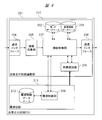
- FIG. 2 is a block diagram illustrating an example of a configuration of the autonomous traveling control ECU 201 included in the in-vehicle system 10 of FIG.
- the autonomous traveling control ECU 201 includes an autonomous traveling control logic unit 210 and a power supply circuit 211.
- the power supply circuit 211 supplies power to the reconfiguration circuit 209.
- the autonomous traveling control logic unit 210 power is supplied to each functional block other than the reconfiguration circuit 209 by a power circuit (not shown).
- the autonomous running control logic unit 210 includes communication interfaces 204 and 208 (hereinafter, collectively referred to as “communication interface 204”), an information collection unit 205, a power supply control unit 206, a function control unit 207, A reconfiguration circuit 209, a mode database 202, a processing item database 203, and a power control database 212 are included.
- the function control unit 207 holds a circuit database (not shown) to be described later.
- the communication interface 204 is an interface that communicates with a predetermined protocol such as CAN used in an in-vehicle system.
- the autonomous traveling control ECU 201 is connected to another device via the communication interface 204, and transmits and receives data.
- the autonomous traveling control ECU 201 is connected to the camera 101, the radar 102, the host vehicle position sensor 103, the automatic driving button 104, and the wireless communication device 105 via the communication interface 204.
- the autonomous travel control ECU 201 is connected to the auxiliary control ECU 106, the brake control ECU 107, the engine control ECU 108, and the power steering control ECU 109 via the communication interface 208, respectively.
- the information collecting unit 205 collects sensor information from the camera 101, the radar 102, and the vehicle position sensor 103 input from the communication interface 204, and an automatic driving control signal from the automatic driving button 104, and collects sensor information and The automatic operation control signal is periodically transferred to the function control unit 207.
- the information collection unit 205 when the information collection unit 205 receives the update information including the autonomous travel control processing information, the circuit data to be updated, and the power supply control data from the wireless communication device 105, the information collection unit 205 stores the circuit data to be updated in a circuit database (not shown), and 202, the contents of the processing item database 203, and the power control database 212 are updated.
- the wireless communication device 105 may be configured to be provided in the autonomous travel control ECU 201, for example.
- the information collecting unit 205 is connected to each database included in the autonomous traveling control logic unit 210 via a control line (not shown). An example of the update information processing will be described later with reference to FIG.
- the function control unit 207 refers to the mode database 202 based on the mode determination signal such as the sensor information and the automatic driving control signal acquired from the information collecting unit 205, and first, the highway approach mode, the automatic parking mode, or the ECU abnormality The operation mode such as the mode is determined.
- processing information indicating how the reconfiguration circuit 209 performs the arithmetic processing required in the operation mode is determined.
- this processing information means the number of divisions of the circuit area of the reconfigurable circuit 209, circuit data for updating each circuit area, calculation time, and the like. Details of the mode database 202 and the processing item database will be described with reference to FIGS. 3 and 4 to be described later.
- the function control unit 207 changes the reconfiguration circuit 209 based on the processing information described above, and causes the reconfiguration circuit 209 to perform the processing of the operation mode.
- a dotted arrow between the function control unit 207 and the reconfiguration circuit 209 indicates transfer of circuit data for the function control unit 207 to reconfigure a circuit from a circuit database (not shown) and a completion notification thereof.
- a solid line arrow between the function control unit 207 and the reconfiguration circuit 209 indicates a process execution instruction, execution data, and transfer of the execution result.
- the function control unit 207 outputs a control command such as a brake and a driving force through the communication interface 208 based on the processing result performed by the reconfiguration circuit 209.
- the reconfiguration circuit 209 is a circuit that executes predetermined processing on data, and is configured by hardware such as an FPGA that can change the circuit configuration.
- the function control unit 207 changes the circuit configuration in accordance with the processing information described above, and executes predetermined processing.
- the power supply control unit 206 acquires mode information from the function control unit 207 and an internal timer value managed by the function control unit 207.
- the internal timer value here is a counter value incremented by the internal clock.
- the power control unit 206 synchronizes by updating the internal timer value of the power control unit 206 based on the acquired internal timer value.
- the power control database 212 stores information related to a power control schedule such as a control signal to the power circuit 211 and timing.
- the power control unit 206 performs power control so as to increase or decrease the current supplied from the power circuit 211 based on the power control database 212 and the above-described internal timer value.
- the power supply control database 212 will be described later with reference to FIG. Details of the power supply control process will be described later with reference to FIGS. 4 and 5.
- the power supply circuit dedicated to the reconfiguration circuit 209 has been described here, the power supply circuit 211 may be a power supply circuit that supplies power to the entire autonomous traveling control logic unit 210.
- Each function unit of the autonomous traveling control logic unit 210 that is, the information collecting unit 205, the function control unit 207, and the power source control unit 206 is a program executed by the autonomous traveling control logic unit 210 or a logic circuit that performs a predetermined operation, for example, Configured by FPGA. From the viewpoint of functional safety of automatic driving, each functional unit of the autonomous traveling control logic unit 210 may be configured by a processor having a plurality of cores adopting a lockstep method.
- the autonomous traveling control logic unit 210 may be physically configured on one electronic control device, or logically or physically on a plurality of electronic control devices.
- the program of each functional unit described above may operate in a separate thread on the same electronic control device, or may operate on a virtual electronic control device constructed on the resources of a plurality of electronic control devices. Good.
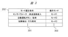
- FIG. 3 is an explanatory diagram of the mode database 202 included in the autonomous traveling control logic unit 210 of FIG.
- the mode database 202 is referred to by the function control unit 207 in FIG. 2 and associates information acquired from the information collection unit 205 with an operation mode to be selected.
- the mode database 202 has a mode selection condition 301 for selecting an operation mode based on information acquired from the information collection unit 205 and an operation mode 302 selected by the mode selection condition 301.
- the mode selection condition 301 is determined to have entered the expressway based on parameter information of external recognition sensors such as the camera 101, the radar 102, and the own vehicle position sensor 103 shown in FIG.
- the case may be the first mode selection condition, and in the operation mode 302, the first operation mode may be determined as the mode 1.
- the mode selection condition 301 the case where the control signal for automatically parking by the automatic operation button 104 in FIG. 1 is received as the second mode selection condition.
- the second operation mode is set to mode 2. You may judge.
- the third operation mode may be determined as mode 3.
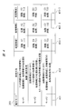
- FIG. 4 is an explanatory diagram of the processing item database 203 included in the autonomous traveling control logic unit 210 of FIG.
- the processing item database 203 is referred to by the function control unit 207 in FIG. 2 and associates the operation mode 302 with the processing content of the corresponding mode.
- This processing item database 203 describes, for each operation mode 401, processing method 402 and processing information 1 (403-1) to processing information 3 (403-3) (when processing information is collectively referred to as “processing information 403”). )).
- the processing method 402 designates the order of single or plural processing to be performed, the circuit reconfiguration procedure, and the like.
- the processing information 403 is processing information specified by the processing method 402.
- the operation mode 401 is mode 1
- one circuit area is provided on the reconfiguration circuit 209 in FIG. 2, and the processing information 1 (403-1) is processed on the circuit area.
- the processing method 402 holds that processing (403-2) and processing information 3 (403-3) are processed in order.
- the circuit data A1 for executing the first processing in mode 1 and the processing time T11 may be held as processing information 1 (403-1).
- the processing time T13 may be held as processing information 3 (403-3).
- the first process in mode 1 is a sensing process
- the second process in mode 1 is a behavior prediction process for a vehicle or a pedestrian
- the third process in mode 1 is a travel route calculation of the vehicle. It is good also as processing.
- the circuit area is divided into two, and processing of processing information 1 (403-1) and processing information 2 (403-2) is sequentially processed in one area.
- the processing method 402 may hold that the processing of the processing information 3 (403-3) is performed in the other area.
- the circuit data B1 to B3 for executing the first to third processes of the mode 2 and the respective processing times T21 to T23 are held as the processing information 403. May be.
- any one of the first to third processes in mode 2 may be an empty parking space search process.
- the operation mode 401 is mode 3
- the circuit area is divided into three and each of processing information 1 (403-1), processing information 2 (403-2), and processing information 3 (403-3) Processing in parallel may be held as the processing method 402.
- the circuit data C1 to C3 for executing the first to third processes of the mode 3 and the respective processing times T31 to T33 are held as the processing information 403. May be.
- any of the first to third processes in mode 3 may be a track securing process for safely stopping the vehicle.
- processing information 403 Although an example in which three pieces of information (processing information 1 (403-1) to processing information 3 (403-3)) are held as the processing information 403 is shown here, four or more pieces of information may be held. Good.
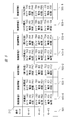
- FIG. 5 is an explanatory diagram of the power control database 212 included in the autonomous driving control logic unit 210 of FIG.
- the power control database 212 stores information related to a power control schedule such as a control signal and timing to the power circuit 211.
- the power supply control database 212 is referred to by the power supply control unit 206 of FIG. 2, and the control information 0 (503-0) to the control information 6 (503-6) (power supply) which are the power control contents of the operation mode 501 and the operation mode 501.
- control information 503 When the control information is collectively referred to, it is described as “power control information 503”).
- the timer value TA0 is a timer value that takes into account the timing at which the connection circuit to the interface with the function control unit 207 in FIG.
- the load current value IA0 is a load current value of the reconfiguration circuit 209 during writing.
- a timer value TA1 that considers the timing to start writing circuit data A1 for executing the first process of mode 1 to the reconfiguration circuit 209, a load current value IA1 of the reconfiguration circuit 209 being written, and a processing time PA1 are obtained. It may be held as control information 1 (503-1).
- the timer value TA2 in consideration of the timing at which the first process of mode 1 is started, the load current value IA2 of the reconfiguration circuit 209 that is executing the first process, and the process You may make it hold
- the timer value TA3 in consideration of the timing to start writing the circuit data A2 for executing the second process of mode 1 to the reconfiguration circuit 209, the load current of the reconfiguration circuit 209 being written
- the value IA3 and the processing time PA3 may be held.
- the timer value TA4 in consideration of the timing at which the second process of mode 1 is started, the load current value IA4 of the reconfiguration circuit 209 that is executing the second process, and the process You may make it hold
- the timer value TA5 in consideration of the timing to start writing the circuit data A3 for executing the third process of mode 1 to the reconfiguration circuit 209, the load current of the reconfiguration circuit 209 being written
- the value IA5 and the processing time PA5 may be held.
- the control information 6 (503-6) includes a timer value TA6 in consideration of the timing at which the third process of mode 1 is started, the load current value IA6 of the reconfiguration circuit 209 that is executing the third process, and the process You may make it hold
- Each load current value may hold, for example, a temporal average value of the load current.
- the power supply circuit 211 in FIG. 2 supplies power only to the reconfiguration circuit 209, but even if the power supply circuit 211 is configured to supply power to the entire autonomous traveling control logic unit 210. Good. In that case, the load current value of the entire autonomous traveling control logic unit 210 is stored in the power supply control database 212.
- the timer value is, for example, a counter value incremented by an internal clock, and is managed by the function control unit 207 in FIG. 2 and used for synchronization with the power supply control unit 206.
- This timer value takes into account the signal delay between the function control unit 207 and the power supply control unit 206 and the control delay from when the power supply control unit 206 starts the power supply control process until the supply current of the power supply circuit 211 increases or decreases.
- the supply current of the power supply circuit 211 is adjusted so as to increase or decrease.
- This power supply control database 212 may store each numerical value based on an actual measurement value or a simulation value before operating as an in-vehicle system, or a processing item database acquired by the power supply control unit 206 from the function control unit 207. It may be created and stored based on each piece of information 203.
- the power supply control information 503 may include a voltage value, a current value, or a control code for controlling the supply current of the power supply circuit 211.
- FIG. 6 is a flowchart showing an example of the power control process in the power control unit 206 of FIG.
- the power control database 212 is created and stored in advance, and the power control unit 206 manages the processing order using the internal control ID.
- the internal control ID indicates a number of control information 0 to 6 in the power supply control information 503 in FIG. Further, description will be made assuming that the function control unit 207 and the power supply control unit 206 in FIG. 2 are each provided with an internal timer.
- step S600 when the power supply control unit 206 starts the power supply control process (step S600), the power supply control unit 206 acquires mode information and a timer value from the function control unit 207 before the reconfiguration circuit calculation is started. The timer value is updated (step S601).
- step S601 the power supply control unit 206 determines whether or not the operation mode is the same as the previous mode value (step S602). If it is determined in step S602 that the operation mode is different from the previous mode value (NO), the power supply control unit 206 sets the internal control ID to 0 (step S603).
- the power supply control unit 206 sets the internal control ID to 1 (step S604). This determines whether or not the process of writing the connection circuit to the interface with the function control unit 207 in the reconfiguration circuit 209 is based on whether or not the operation mode is different from the previous one.
- the ID information of the connection circuit described above may be obtained from the function control unit 207 to determine whether or not it is the same as the previous time.
- the power supply control unit 206 refers to the power supply control database 212 and waits until the timer value indicated by the internal control ID matches the internal timer value of the power supply control unit 206. (Step S605).
- step S605 If it is determined in step S605 that the timer values match (YES), the load current value and processing time indicated by the internal control ID are transmitted to the power supply circuit 211 as a power supply control instruction (step S606).
- the power supply circuit 211 supplies a reference current value until receiving a power supply control instruction.
- the power supply circuit 211 increases or decreases the supply current so that the load current value indicated by the internal control ID is obtained.
- the reference current value is supplied again.
- the reference current value may be set in consideration of the leakage current when the supply target is only the reconfiguration circuit 209. In the case of supplying power to the entire autonomous traveling control logic unit 210, it may be set in consideration of a load current other than that of the reconfiguration circuit 209.
- the power supply control unit 206 determines whether or not there is a next process (step S607). Whether or not there is the next processing can be determined by the power supply control unit 206 from the power supply control database 212 of FIG.
- step S607 If it is determined in step S607 that the next process is present (YES), the power supply control unit 206 increments the internal process ID (step S608) and returns to the process in step S605 to prepare for the next process.
- step S607 If it is determined in step S607 that there is no next process (NO), the power supply control unit 206 ends the power supply control process (step S609).
- FIG. 7 is a sequence diagram showing an example of the power control process in the power control unit 206 of FIG.
- FIG. 7 illustrates an example in which the operation mode 501 of the power supply control database 212 described above with reference to FIG.
- the power control database 212 is created and stored in advance.
- the function control unit 207 acquires mode information from the mode database 202 and confirms whether or not the mode is switched. Further, an internal timer value managed by the function control unit 207 is acquired (step S700). Here, an example in which the mode is switched is shown.
- the function control unit 207 sends the mode information and the timer value to the power supply control unit 206 (step S701).
- the power control unit 206 updates the internal timer value of the power control unit 206 based on this timer value (step S702).
- control information 0 (503-0) relating to the reconfiguration of the connection circuit to the interface with the function control unit 207 held in the power control database 212 the timer value and the internal timer value of the power control unit 206 are Are matched, the load current value and the processing time are transmitted to the power supply circuit 211 as a power supply control instruction (step S704).
- the power supply circuit 211 increases or decreases the supply current to the reconfiguration circuit 209 from the reference current value so as to become the load current value indicated by the internal control ID. (Step S705).
- the function control unit 207 writes connection circuit data with the interface with the function control unit 207 in the reconfiguration circuit 209 slightly after the start of the current control in the process of step S705, for example, about 1 millisecond or less (step S707). ).
- the reconfiguration circuit 209 reconfigures the interface connection circuit (step S708), and notifies the function control unit 207 of the completion of writing (step S709). Then, the power supply control unit 206 refers to the control information 1 (503-1) relating to the reconfiguration of the circuit data A1 held in the power supply control database 212, and determines the timer value and the internal timer value of the power supply control unit 206. Are matched, the load current value and the processing time are transmitted to the power supply circuit 211 as a power supply control instruction (step S710).
- the power supply circuit 211 increases or decreases the supply current to the reconfiguration circuit 209 from the reference current value so as to become the load current value indicated by the internal control ID. (Step S711).
- the function control unit 207 writes the data of the circuit A1 in the reconfiguration circuit 209 slightly later than the current control start by the processing of S711 (step S713).
- the reconfiguration circuit 209 reconfigures the circuit A1 (step S714), and notifies the function controller 207 of the completion of writing (step S715).
- the power supply control unit 206 refers to the control information 2 (503-2) related to the first process stored in the power supply control database 212, and determines the timer value and the internal timer value of the power supply control unit 206. Are matched, the load current value and the processing time are transmitted to the power supply circuit 211 as a power supply control instruction (step S716).
- the power supply circuit 211 increases or decreases the supply current to the reconfiguration circuit 209 from the reference current value to the load current value indicated by the internal control ID, and again when the processing time indicated by the internal control ID ends.
- the reference current value is restored (step S717).
- the function control unit 207 notifies the reconfiguration circuit 209 of the execution instruction of the first process slightly after the start of the current control of the process of step S717 (step S719).
- the reconfiguration circuit 209 executes the calculation of the first process (step S720), and notifies the function control unit 207 of the completion of the execution together with the calculation result, in other words, the process result (step S721).
- the function control unit 207 may hold the calculation result of the first process and use it for the calculation of the subsequent process.
- step S722 confirms the presence or absence of the next process.
- the operation mode 501 is mode 1 and the second process is the next process.
- the function control unit 207 transmits a power control continuation instruction to the power control unit 206 (step S723).
- the power control unit 206 refers to the control information 3 (503-3) relating to the reconfiguration of the circuit data A2 held in the power control database 212, and the timer value matches the internal timer value of the power control unit 206. Then, the load current value and the processing time are transmitted to the power supply circuit 211 as a power supply control instruction (step S724).
- circuit data A2 and second processing using the same circuit data A3 and third processing using the same are performed.
- the function control unit 207 confirms the presence / absence of the next process (step S753).
- the operation mode 501 is mode 1 and there is no next processing
- an end instruction is sent to the power supply control unit 206 (step S754), and the power supply control unit 206 receives it and waits for reception (step S755).
- the sequence of the power control process is completed.
- the function control unit 207 and the power supply control unit 206 have been described as including internal timers, but may include a common internal timer.
- the autonomous traveling control logic unit 210 performs processing periodically based on the collected sensor information, automatic driving control signals, and the like. Therefore, as described above, it is not always necessary for the power supply control unit 206 to acquire each piece of information from the function control unit 207 every period.
- a delay may be given to the start time of the reconfiguration processing or arithmetic processing of the reconfiguration circuit 209.
- the power supply circuit 211 also supplies power other than the reconfiguration circuit 209
- calculation may be performed while avoiding a section in which the load fluctuation of the reconfiguration circuit 209 occurs with respect to the blocks of other autonomous traveling control logic units.
- the computation in the same section may be made redundant.
- FIG. 8 is a sequence diagram showing an example of operation mode expansion in the in-vehicle system 10 of FIG.
- FIG. 8 shows an example of adding an operation mode of automatic operation via a wireless network by OTA (Over-The-Air) from a server on the cloud, for example.
- OTA Over-The-Air
- step S1100 when an operation mode addition instruction is set in the server (step S1100), information on the operation mode to be added is transferred to the wireless communication device 105 of the in-vehicle system (S1101).
- the information regarding the operation mode includes, for example, the contents of the mode database 202, the processing item database 203, and the power control database 212, and circuit data of the operation mode to be added.
- the wireless communication device 105 transfers the received additional information to the autonomous travel control logic unit 210 (step S1102). Then, the autonomous traveling control logic unit 210 stores the circuit data in the circuit database (step S1103).
- the autonomous traveling control logic unit 210 sets the operation mode 501 and control information 503 to be added to the power supply control database 212 (step S1104). Further, the autonomous traveling control logic unit 210 sets the operation mode 401 to be added, the processing method 402, and the processing information 403 in the processing item database 203 (step S1105).
- the autonomous traveling control logic unit 210 adds the operation mode selection condition 301 and the operation mode 302 to the mode database 202 (S1106) and completes the processing.
- circuit data and processing method used in the added operation mode are introduced to the autonomous driving control unit without affecting the operating mode in use. be able to.
- the power supply control unit 206 obtains information on the reconfiguration and calculation schedule from the function control unit 207 that controls the reconfiguration and calculation of the reconfiguration circuit 209, and the load caused by the reconfiguration and calculation of the reconfiguration circuit 209.
- the power supply circuit 211 can be controlled to increase or decrease the supply current to the reconstruction circuit 209 prior to the fluctuation.
- the transient increase and decrease of the output voltage of the power supply circuit 211 can be reduced, and the highly reliable autonomous traveling control ECU 201 can be provided at low cost and in a small area.
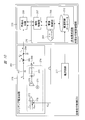
- FIG. 9 is a block diagram showing another example of the autonomous traveling control ECU 201 in FIG.
- the autonomous traveling control ECU 201 includes an autonomous traveling control logic unit 210 and a power supply circuit 211.
- the power circuit 211 supplies power to the reconfiguration circuit 209, and power supply to the autonomous traveling control logic unit 210 other than the reconfiguration circuit 209 is performed by a power circuit (not shown).
- the autonomous traveling control ECU 201 in FIG. 9 is significantly different from the autonomous traveling control ECU 201 in FIG. 2 in that the power control unit 206 and the power control database 212 are included in the power circuit 211 instead of the autonomous traveling control logic unit 210.
- Basic processing and control may be considered to be the same as described above with reference to FIG.
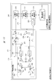
- FIG. 10 is an explanatory diagram showing an example of a configuration in the autonomous traveling control ECU 201 according to the second embodiment.
- the autonomous traveling control ECU 201 includes an autonomous traveling control logic unit 210, a switching power supply circuit 275, and a power supply circuit 277.
- the autonomous traveling control logic unit 210 includes a reconfiguration circuit 209 and a non-reconfiguration circuit 276.
- the non-reconfigurable circuit 276 includes a function control unit 207, a power control unit 206, a power control database 212, and a D / A (Digital / Analog) converter 263.
- the function control unit 207 holds a circuit database (not shown).
- the switching power supply circuit 275 supplies power to the reconfiguration circuit 209, and the power supply circuit 277 supplies power to the non-reconfiguration circuit 276.
- the autonomous travel control ECU 201 has a plurality of communication interfaces, an information collection unit, a mode database, and a processing item database, as in FIG. 1 of the first embodiment.
- the power supply control unit 206 acquires mode information from the function control unit 207 and an internal timer value managed by the function control unit 207. Further, the power control unit 206 achieves synchronization by updating the internal timer value of the power control unit 206 based on the acquired internal timer value.
- the power supply control database 212 stores information related to a power supply control schedule such as a control signal to the switching power supply circuit 275 and timing.
- the power supply control unit 206 performs power supply control so as to increase or decrease the supply current of the switching power supply circuit 275 based on the power supply control database 212 and the above-described internal timer value.
- the D / A converter 263 is used to convert the power supply control signal from a digital value to an analog value and transmit it to the switching power supply circuit 275. Details of the power supply control database 212 will be described later with reference to FIG.
- the switching power supply circuit 275 includes an inductor current control unit 274, switches 267 and 268, an inductor 265, and a capacitor 264.
- PWM Pulse Width Modulation
- the inductor current control unit 274 increases or decreases the inductor current IL flowing through the inductor 265 by performing ON / OFF control of the switches 267 and 268. Since the output voltage Vo1 generated by the output current Io1 flowing through the reconfiguration circuit 209 has a large ripple due to the fluctuation of the inductor current IL, the output voltage Vo1 is smoothed by the capacitor 264 to a voltage close to DC.
- the inductor current control unit 274 includes a switch driver 269, a comparator 270, a triangular wave generator 271, an error detector 272, and an adder 273.
- the reference voltage VREF1 and the observed output voltage Vo1 are input to the error detector 272, and the difference between the two input is output from the error detector 272. The difference is input to the comparator 270 together with the output of the triangular wave generator 271.
- the comparator 270 outputs a PWM signal corresponding to the above-described difference.
- the switch driver 269 performs ON / OFF control of the switches 267 and 268 in accordance with the PWM signal, and adjusts the inductor current IL.
- the switching power supply circuit 275 operates so as to maintain the output voltage Vo1 constant by such a feedback system, and steps down the input voltage Vin.
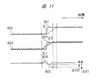
- FIG. 11 is a schematic diagram of changes in the inductor current waveform and output voltage to show the effect of power control by the power control unit 206 in FIG.
- the output voltage 805 has a large ⁇ V1 in accordance with the insufficient charge amount (corresponding to the area ⁇ in FIG. 11). A voltage drop occurs.
- the power supply control signal VPLS is a voltage pulse signal that is added to VREF1 via the adder 273 before the load fluctuation timing.
- the inductor current IL can be controlled to increase or decrease before the timing when the load current 801 changes suddenly.
- the areas of ⁇ 1 and ⁇ 2 can be matched as in the inductor current 803 in FIG.
- FIG. 12 is an explanatory diagram of the power supply control database 212 included in the autonomous traveling control ECU 201 of FIG.
- the power supply control database 212 stores information related to a power supply control schedule such as control signals and timing to the switching power supply circuit 275 in FIG.
- the power supply control database 212 is referred to by the power supply control unit 206, and control information 0 (513-0) to control information 6 (513-6) (generic name of power supply control information) which are the power control contents of the operation mode 511 and the corresponding mode. In this case, it is described as “power control information 513”.
- the control information 0 (513-0) includes the timer value TA01, the power supply control signal voltage value VA01, the pulse width time PA01, the timer value TA02, and the power supply control signal voltage value. VA02 and pulse width time PA02 may be held.
- the timer value TA01 is a timer value in consideration of the timing at which the connection circuit to the interface with the function control unit 207 starts to be written in the reconfiguration circuit 209.
- the timer value TA02 is a timer value that takes into account the timing at which the connection circuit is written to the reconfiguration circuit 209.
- the timer value TA11 in consideration of the timing to start writing the circuit data A1 for executing the first processing of mode 1 to the reconfiguration circuit 209, the voltage value VA11 of the power control signal
- the pulse width time PA11, the timer value TA12 in consideration of the timing to finish writing the circuit data A1 to the reconfiguration circuit 209, the voltage value VA12 of the power supply control signal, and the pulse width time PA12 may be held.
- the timer value TA21, the power control signal voltage value VA21, the pulse width time PA21, and the first process are executed in consideration of the timing at which the first process of the mode 1 is started.
- the timer value TA22 in consideration of the end timing, the voltage value VA22 of the power supply control signal, and the pulse width time PA22 may be held.
- the timer value TA31, the voltage value VA31 of the power supply control signal, the pulse width in consideration of the timing to start writing the circuit data A2 for executing the second process of mode 1 to the reconfiguration circuit 209
- the timer value TA32, the voltage value VA32 of the power supply control signal, and the pulse width time PA32 may be held in consideration of the time PA31, the timing at which the circuit data A2 is written to the reconfiguration circuit 209.
- the timer value TA41, the voltage value VA41 of the power supply control signal, the pulse width time PA41, and the second process are executed in consideration of the timing at which the second process of the mode 1 is started.
- the timer value TA42 in consideration of the end timing, the voltage value VA42 of the power supply control signal, and the pulse width time PA42 may be held as the control information 4 (513-4).
- the timer value TA51, the voltage value VA51 of the power supply control signal, the pulse width in consideration of the timing to start writing the circuit data A3 for executing the third process of mode 1 to the reconfiguration circuit 209
- the timer value TA52, the voltage value VA52 of the power supply control signal, and the pulse width time PA52 may be held in consideration of the time PA51, the timing at which the circuit data A3 is written to the reconfiguration circuit 209.
- the timer value TA61, the voltage value VA61 of the power supply control signal, the pulse width time PA61, and the third process are executed in consideration of the timing at which the third process of mode 1 is started.
- the timer value TA62, the voltage value VA62 of the power supply control signal, and the pulse width time PA62 taking into account the end timing may be held.
- the timer value is a counter value incremented by an internal clock, is managed by the function control unit 207, and is used for synchronization with the power supply control unit 206.
- This timer value is a signal delay between the function control unit 207 and the power supply control unit 206 or a control delay from when the power supply control unit 206 starts the power supply control process until the supply current of the switching power supply circuit 275 increases or decreases.
- the supply current of the switching power supply circuit 275 is adjusted to increase or decrease before the load current of the reconfiguration circuit 209 fluctuates.
- the power supply control database 212 may store each numerical value based on an actual measurement value or a simulation value before operating as an in-vehicle system, or may be a processing item database acquired by the power supply control unit 206 from the function control unit 207. You may create and store based on each information.
- the voltage pulse signal is added to the reference voltage VREF1 as the power supply control signal has been described, but it may be added to the output voltage value input to the error detector 272. Further, a power supply control signal that temporarily increases the response speed of the feedback loop of the switching power supply circuit 275 may be used so as to cope with a sudden change in the load current.
- the gain of the comparator 270 may be increased, or the frequency of the triangular wave generator 271 may be increased. Further, instead of controlling the switching power supply circuit by the PWM control method, a hysteresis control method may be used.
- an observation unit for monitoring the power supply voltage supplied to the reconfiguration circuit 209 is provided, for example, with the voltage value monitored by the power supply control unit 206 and the set voltage initially set in the power supply control database 212. It may be compared with a certain control voltage, and the power supply control database 212 may be updated according to the error between the two.
- the voltage may be divided by a high resistance and observed by the power supply control unit 206 through an operational amplifier and an A / D (Analog / Digital) converter.
- a / D Analog / Digital
- the value of (control voltage value ⁇ observed voltage value) may be added to the control voltage value of the power supply control database 212.
- a correction function using (control voltage value ⁇ observed voltage value) as an input value may be incorporated in the power supply control unit 206 in advance, and the power supply control database 212 may be updated based on the output value.
- FIG. 13 is an explanatory view showing another configuration example of the autonomous traveling control ECU 201 of FIG.
- a switching power supply circuit 275 shown in FIG. 13 is a single-inductor-two-output SIMO (Single Inductor Multi-Output) power supply circuit, and supplies power to the reconfiguration circuit 209 and the non-reconfiguration circuit 276. Since the SIMO power supply circuit has a plurality of outputs with one inductor, it is a technology that can contribute to cost reduction and area saving.
- SIMO Single Inductor Multi-Output
- the switching power supply circuit 275 includes an inductor current control unit 298, switches 283, 284, 286, 287, an inductor 285, and capacitors 281, 282, as shown.
- the inductor current control unit 298 increases or decreases the inductor current IL flowing through the inductor 285 by performing ON / OFF control of the switches 286 and 287.
- the output destination of the power supply voltage is changed to the reconfiguration circuit 209 or the non-reconfiguration circuit 276 by performing ON / OFF control of the switches 283 and 284.
- These switches 283 and 284 and the inductor current control unit 298 constitute an output switching unit.
- the output voltage Vo1 generated by the output current Io1 flowing through the reconfiguration circuit 209 has a large ripple due to the fluctuation of the inductor current IL, the output voltage Vo1 is smoothed by using the capacitor 281 to be a voltage close to DC.
- the inductor current control unit 298 includes switch drivers 288 and 289, comparators 290 and 291, a triangular wave generator 292, error detectors 293 and 294, adders 295, 296 and 297 and the like.
- the power control signal VPLS sent from the power control unit 206 through the D / A converter 263 is added to the reference voltage VREF1 by the adder 296.
- the output voltage Vo1 and the output voltage Vo2 added by the adder 295 are added. These added voltages are input to the error detector 293, and a difference between these voltages is output from the error detector 293.
- the difference is input to the comparator 290 together with the output of the triangular wave output device 292.
- the comparator 290 outputs a PWM signal corresponding to the above difference.
- the switch driver 288 performs ON / OFF control of the switches 286 and 287 according to the PWM signal, and adjusts the inductor current IL.
- the power supply control signal VPLS is also added to the reference voltage VREF2 by the adder 296, and is input to the error detector 294 together with the observed output voltage Vo2, and the difference between the two is output from the error detector 294.
- the difference is input to the comparator 291 together with the output of the triangular wave output device 292.
- the comparator 291 outputs a PWM signal corresponding to the above difference.
- the switch driver 289 performs ON / OFF control of the switches 283 and 284 in accordance with the PWM signal, and adjusts the output destination.
- the switching power supply circuit 275 operates to maintain the output voltage Vo1 and the output voltage Vo2 constant by such a feedback system, and steps down the input voltage Vin.
- the power supply control signal VPLS is a voltage pulse signal to be added to the reference voltages VREF1 and VREF2 before the timing of this load change, and is stored in advance in the control information database 212, for example.
- the inductor current IL can be controlled to increase or decrease before the timing when the load current suddenly changes, and the voltage transient fluctuation of the output voltage can be reduced.
- the power supply circuit can be controlled to increase or decrease the supply current to the reconfiguration circuit 209 prior to the load fluctuation caused by the reconfiguration and calculation of the reconfiguration circuit 209 using a simple analog circuit.
- the transient increase and decrease of the output voltage of the switching power supply circuit 275 can be reduced, and the highly reliable autonomous traveling control ECU 201 can be provided at low cost and in a small area.
- a part of the configuration of one embodiment can be replaced with the configuration of another embodiment, and the configuration of another embodiment can be added to the configuration of one embodiment. .
- each of the above-described configurations, functions, processing units, processing means, and the like may be realized by hardware by designing a part or all of them with, for example, an integrated circuit.
- Each of the above-described configurations, functions, and the like may be realized by software by interpreting and executing a program that realizes each function by the processor.
- Information such as programs, tables, and files for realizing each function can be stored in a recording device such as a memory, a hard disk, an SSD (Solid State Drive), or a recording medium such as an IC card, an SD card, or a DVD.
- control lines and information lines indicate what is considered necessary for the explanation, and not all the control lines and information lines on the product are necessarily shown. Actually, it may be considered that almost all the components are connected to each other.
Abstract
The present invention reduces transient increases/decreases in the power to be supplied to a reconfigurable circuit which is a logic circuit with a changeable circuit configuration. An autonomous travel control ECU 201 has a reconfigurable circuit 209, a functional control unit 207, a power supply circuit 211, and a power supply control unit 206. The reconfigurable circuit 209 is a logic circuit that can be reconfigured. The functional control unit 207 determines the operation mode of the reconfigurable circuit 209 on the basis of a mode determination signal and controls the reconfiguration of the reconfigurable circuit 209 on the basis of the determination result. The power supply circuit 211 supplies power to the reconfigurable circuit 209. The power supply control unit 206 controls the power supply circuit. The power supply control unit 206 controls the load current generated by the power supply circuit 211 before a the load of the reconfigurable circuit 209 fluctuates, on the basis of power supply control information that is information for controlling the power supply circuit 211.
Description
本発明は、電子制御装置、車載システムおよび電源制御方法に関し、特に、回路構成を変更可能な論理回路に電力供給する電源の制御に有効な技術に関する。
The present invention relates to an electronic control device, an in-vehicle system, and a power supply control method, and more particularly to a technique effective for controlling a power supply that supplies power to a logic circuit whose circuit configuration can be changed.
自動運転は、事故数低減、渋滞解消をはじめとした様々な社会課題を解決しうるシステムであり、世界的にその実用化に向けた取り組みが年々活発化している。自動運転システムでは、カメラやレーダなどのセンサ入力から車両や歩行者および白線などを検出して運転者に伝達したり、ブレーキやステアリングを制御したりする必要がある。そのため、高度な認識アルゴリズムや複数のアルゴリズムの同時処理が求められる。
Autonomous driving is a system that can solve various social issues such as reducing the number of accidents and eliminating traffic jams. In an automatic driving system, it is necessary to detect a vehicle, a pedestrian, a white line, and the like from sensor inputs such as a camera and a radar, and transmit them to the driver, or control a brake and a steering. Therefore, advanced recognition algorithms and simultaneous processing of a plurality of algorithms are required.
この要求に対応するため、自動運転システムでは、CPUに加えて、FPGA(Field-Programmable Gate Array)を用いて高性能化する検討が進められている。
In order to respond to this requirement, in the automatic driving system, in addition to the CPU, studies are being made to improve the performance by using FPGA (Field-Programmable Gate Array).
FPGAは、論理回路を変更可能な再構成回路であり、複数のハードウェアに備える処理を1つの回路上にて行うことができるという特長を有する。当然のことながら、このような論理回路に限らず電子回路全般は、電源回路からの電源供給があってはじめて用を成す。
The FPGA is a reconfigurable circuit that can change the logic circuit, and has a feature that it is possible to perform processing provided in a plurality of hardware on one circuit. As a matter of course, not only such a logic circuit but also an electronic circuit in general can be used only when power is supplied from a power supply circuit.
一方、ポータブル・コンピュータをはじめとした電子機器においては、所定の動作モードの際に、電力管理スキームを採用して電子機器中の選択したアセンブリの機能を無効または有効に適宜切り替えることにより省消費化を図っている。
On the other hand, in electronic devices such as portable computers, power consumption is reduced by appropriately switching the function of the selected assembly in the electronic device by using a power management scheme in a predetermined operation mode. I am trying.
電子機器のアセンブリの機能が有効または無効にされると、その電子機器の負荷が変化して、電源装置からの出力電圧が過渡的に低下および上昇して、データエラーや自動リセットなど引き起こしうる。
When the function of the electronic device assembly is enabled or disabled, the load of the electronic device is changed, and the output voltage from the power supply device is transiently decreased and increased, which may cause data error or automatic reset.
この過渡的な電圧変動を低減するための技術としては、例えば少なくとも1つの回路ブロックの負荷状態をイネーブル信号又はクロック信号の関数として判定し、電源装置の出力電流を少なくとも1つの回路ブロックの負荷状態の関数として、電源装置が出力電流を制御するものがある(例えば特許文献1参照)。
As a technique for reducing the transient voltage fluctuation, for example, the load state of at least one circuit block is determined as a function of an enable signal or a clock signal, and the output current of the power supply apparatus is determined as the load state of at least one circuit block. As a function, there is one in which the power supply device controls the output current (see, for example, Patent Document 1).
また、電源回路の出力電圧の平滑化する技術としては、電源の出力端子とグランド端子との間に出力コンデンサを設けることが広く知られている。
Also, as a technique for smoothing the output voltage of the power supply circuit, it is widely known to provide an output capacitor between the output terminal of the power supply and the ground terminal.
自動運転システムにおいては、歩行者の飛び出しなど突発的なシチュエーションにも瞬時に対応する必要がある。そのため、論理回路の再構成処理を短時間で行う必要がある。再構成処理からアルゴリズム処理に推移する際、論理回路の負荷電流は、短時間で大きく増加する。また、その逆に、アルゴリズム処理から再構成処理に推移する際には、論理回路の負荷電流は、短時間で大きく減少する。
In the automatic driving system, it is necessary to respond instantaneously to sudden situations such as pedestrians jumping out. Therefore, it is necessary to perform the logic circuit reconfiguration processing in a short time. When transitioning from the reconstruction process to the algorithm process, the load current of the logic circuit greatly increases in a short time. On the contrary, when the algorithm process is changed to the reconfiguration process, the load current of the logic circuit is greatly reduced in a short time.
そして、このようなFPGAを負荷とする電源回路は、上記した負荷電流の急激な増加および減少に伴って、それぞれ出力電圧が過渡的に低下および上昇する。
In such a power supply circuit using an FPGA as a load, the output voltage transiently decreases and increases as the load current increases and decreases rapidly.
このような場合において、電源回路の出力電圧がFPGAの許容範囲外となってしまうと、データエラーや自動リセットを誘発する可能性が増大するという問題がある。したがって、FPGAに電流を供給する電源回路は、急激な負荷変動があっても常に定電圧を供給するような機能が求められる。
In such a case, if the output voltage of the power supply circuit falls outside the allowable range of the FPGA, there is a problem that the possibility of inducing a data error or automatic reset increases. Therefore, a power supply circuit that supplies current to the FPGA is required to have a function of constantly supplying a constant voltage even when there is a sudden load fluctuation.
しかしながら、特許文献1の技術は、回路ブロックを制御、つまり、回路ブロックの負荷状態を変化させているイネーブル信号またはクロック信号から回路ブロックの負荷状態を推定するために、電源回路の制御は、必ず負荷変動後になってしまう。その結果、過渡的な電圧変動を十分に抑圧することは難しいと考えられる。
However, in the technique of Patent Document 1, in order to control the circuit block, that is, to estimate the load state of the circuit block from the enable signal or the clock signal that changes the load state of the circuit block, It becomes after the load fluctuation. As a result, it is considered difficult to sufficiently suppress the transient voltage fluctuation.
また、電源回路の出力電圧の平滑化に用いられる出力コンデンサについては、論理回路の負荷上昇が急激であればあるほど大きな容量のコンデンサが必要とされ、コストや実装面積が増大するという懸念がある。
In addition, as for the output capacitor used for smoothing the output voltage of the power supply circuit, a capacitor having a larger capacity is required as the load of the logic circuit increases more rapidly, and there is a concern that the cost and mounting area increase. .
本発明の目的は、回路構成を変更可能な論理回路に供給する電力の過渡的な増減を低減することのできる技術を提供することにある。
An object of the present invention is to provide a technique capable of reducing a transient increase / decrease in power supplied to a logic circuit whose circuit configuration can be changed.
本発明の前記ならびにその他の目的と新規な特徴については、本明細書の記述および添付図面から明らかになるであろう。
The above and other objects and novel features of the present invention will be apparent from the description of this specification and the accompanying drawings.
本願において開示される発明のうち、代表的なものの概要を簡単に説明すれば、次のとおりである。
Of the inventions disclosed in this application, the outline of typical ones will be briefly described as follows.
すなわち、代表的な電子制御装置は、再構成回路、機能制御部、電源回路、および電源制御部を有する。再構成回路は、再構成可能な論理回路である。機能制御部は、車両の動作モードを示すモード判定信号に基づいて、再構成回路の動作モードを判定し、その判定結果に基づいて再構成回路の再構成を制御する。電源回路は、再構成回路に電源電圧を供給する。電源制御部は、電源回路を制御する。
That is, a typical electronic control device has a reconfiguration circuit, a function control unit, a power supply circuit, and a power supply control unit. The reconfigurable circuit is a reconfigurable logic circuit. The function control unit determines the operation mode of the reconfiguration circuit based on the mode determination signal indicating the operation mode of the vehicle, and controls the reconfiguration of the reconfiguration circuit based on the determination result. The power supply circuit supplies a power supply voltage to the reconstruction circuit. The power control unit controls the power circuit.
電源制御部は、電源回路を制御する情報である電源制御情報に基づいて、再構成回路の負荷変動前に電源回路が生成する負荷電流を制御する。
The power supply control unit controls the load current generated by the power supply circuit before the load change of the reconfiguration circuit based on the power supply control information that is information for controlling the power supply circuit.
特に、電源制御情報は、再構成回路の動作モードおよび動作モードに対応する電源回路における制御情報を有する。そして、電源制御部は、機能制御部が判定した動作モードに対応する制御情報を電源制御情報から取得する。
In particular, the power supply control information includes the operation mode of the reconfiguration circuit and the control information in the power supply circuit corresponding to the operation mode. The power supply control unit acquires control information corresponding to the operation mode determined by the function control unit from the power supply control information.
さらに、電源制御情報を格納する電源制御データベースを有する。電源制御部は、機能制御部が判定した動作モードに対応する制御情報を電源制御データベースに格納される電源制御情報から検索する。
Furthermore, it has a power control database that stores power control information. The power control unit searches the power control information stored in the power control database for control information corresponding to the operation mode determined by the function control unit.
本願において開示される発明のうち、代表的なものによって得られる効果を簡単に説明すれば以下のとおりである。
Among the inventions disclosed in the present application, effects obtained by typical ones will be briefly described as follows.
(1)回路構成を変更可能な論理回路である再構成回路に電力を供給する電源回路の出力電圧の過渡的な増減を低減することができる。
(1) A transient increase or decrease in the output voltage of the power supply circuit that supplies power to the reconfiguration circuit, which is a logic circuit whose circuit configuration can be changed, can be reduced.
(2)上記(1)により、信頼性の高い電子制御装置を実現することができる。
(2) According to the above (1), a highly reliable electronic control device can be realized.
以下の実施の形態においては便宜上その必要があるときは、複数のセクションまたは実施の形態に分割して説明するが、特に明示した場合を除き、それらはお互いに無関係なものではなく、一方は他方の一部または全部の変形例、詳細、補足説明等の関係にある。
In the following embodiments, when it is necessary for the sake of convenience, the description will be divided into a plurality of sections or embodiments. However, unless otherwise specified, they are not irrelevant to each other. There are some or all of the modifications, details, supplementary explanations, and the like.
また、以下の実施の形態において、要素の数等(個数、数値、量、範囲等を含む)に言及する場合、特に明示した場合および原理的に明らかに特定の数に限定される場合等を除き、その特定の数に限定されるものではなく、特定の数以上でも以下でもよい。
Further, in the following embodiments, when referring to the number of elements (including the number, numerical value, quantity, range, etc.), especially when clearly indicated and when clearly limited to a specific number in principle, etc. Except, it is not limited to the specific number, and may be more or less than the specific number.
さらに、以下の実施の形態において、その構成要素(要素ステップ等も含む)は、特に明示した場合および原理的に明らかに必須であると考えられる場合等を除き、必ずしも必須のものではないことは言うまでもない。
Further, in the following embodiments, the constituent elements (including element steps and the like) are not necessarily indispensable unless otherwise specified and apparently essential in principle. Needless to say.
同様に、以下の実施の形態において、構成要素等の形状、位置関係等に言及するときは特に明示した場合および原理的に明らかにそうではないと考えられる場合等を除き、実質的にその形状等に近似または類似するもの等を含むものとする。このことは、上記数値および範囲についても同様である。
Similarly, in the following embodiments, when referring to the shape, positional relationship, etc. of components, etc., the shape of the component is substantially the case unless it is clearly specified and the case where it is clearly not apparent in principle. And the like are included. The same applies to the above numerical values and ranges.
また、実施の形態を説明するための全図において、同一の部材には原則として同一の符号を付し、その繰り返しの説明は省略する。なお、図面をわかりやすくするために平面図であってもハッチングを付す場合がある。
In all the drawings for explaining the embodiments, the same members are, in principle, given the same reference numerals, and the repeated explanation thereof is omitted. In order to make the drawings easy to understand, even a plan view may be hatched.
以下、実施の形態を詳細に説明する。
Hereinafter, embodiments will be described in detail.
(実施の形態1)
〈概要〉
本実施の形態1の車載システム10において、自律走行制御ECU201は、再構成可能な論理回路である再構成回路209と、再構成回路209の再構成を制御する機能制御部207と、再構成回路209に電源電圧を供給する電源回路211と、電源回路211を制御する電源制御部206を有する。 (Embodiment 1)
<Overview>
In the in-vehicle system 10 according to the first embodiment, the autonomoustraveling control ECU 201 includes a reconfiguration circuit 209 that is a reconfigurable logic circuit, a function control unit 207 that controls reconfiguration of the reconfiguration circuit 209, and a reconfiguration circuit. A power supply circuit 211 that supplies a power supply voltage to 209 and a power supply control unit 206 that controls the power supply circuit 211 are included.
〈概要〉
本実施の形態1の車載システム10において、自律走行制御ECU201は、再構成可能な論理回路である再構成回路209と、再構成回路209の再構成を制御する機能制御部207と、再構成回路209に電源電圧を供給する電源回路211と、電源回路211を制御する電源制御部206を有する。 (Embodiment 1)
<Overview>
In the in-vehicle system 10 according to the first embodiment, the autonomous
また、自律走行制御ECU201は、機能制御部か207ら再構成回路209に対する複数の処理または複数の処理間の書き換えである演算ID毎に対応した電源制御情報が格納された電源制御データベース212を有する。
Further, the autonomous traveling control ECU 201 has a power control database 212 in which power control information corresponding to each operation ID that is a plurality of processes from the function control unit 207 to the reconfiguration circuit 209 or a rewrite between a plurality of processes is stored. .
電源制御部206は、機能制御部207から受け付けた演算IDに基づいて、電源制御データベース212から電源制御情報を抽出する。そして、抽出した電源制御情報に基づいて、再構成回路209に電源電圧を供給する電源回路211を制御する。
The power control unit 206 extracts power control information from the power control database 212 based on the calculation ID received from the function control unit 207. Based on the extracted power supply control information, the power supply circuit 211 that supplies the power supply voltage to the reconfiguration circuit 209 is controlled.
以下、本発明の実施の形態を図面に基づいて詳細に説明する。
Hereinafter, embodiments of the present invention will be described in detail with reference to the drawings.
〈車載システムの構成例〉
図1は、本実施の形態1による車載システムの構成の一例を示すブロック図である。 <Example configuration of in-vehicle system>
FIG. 1 is a block diagram showing an example of the configuration of an in-vehicle system according to the first embodiment.
図1は、本実施の形態1による車載システムの構成の一例を示すブロック図である。 <Example configuration of in-vehicle system>
FIG. 1 is a block diagram showing an example of the configuration of an in-vehicle system according to the first embodiment.
車載システム10は、例えば車両の自律走行を制御するシステムである。この車載システム10は、図1に示すように、カメラ101、レーダ102、自車位置センサ103、自動運転ボタン104、無線通信装置105、補助制御ECU106、ブレーキ制御ECU(Electronic Control Unit:電子制御装置)107、エンジン制御ECU108、パワーステアリング制御ECU109、および自律走行制御ECU201を備える。
The in-vehicle system 10 is a system that controls the autonomous traveling of the vehicle, for example. As shown in FIG. 1, the in-vehicle system 10 includes a camera 101, a radar 102, a vehicle position sensor 103, an automatic operation button 104, a wireless communication device 105, an auxiliary control ECU 106, a brake control ECU (Electronic Control Unit). 107, an engine control ECU 108, a power steering control ECU 109, and an autonomous travel control ECU 201.
カメラ101、レーダ102、および自車位置センサ103は、車両の外界状況を認識する外界認識センサである。カメラ101およびレーダ102は、外界の認識や対象物までの距離を求めるセンサである。
The camera 101, the radar 102, and the own vehicle position sensor 103 are external recognition sensors that recognize the external environment of the vehicle. The camera 101 and the radar 102 are sensors for recognizing the outside world and obtaining a distance to an object.
自車位置センサ103は、GPS(Global Positioning System)などによって自車位置を検出するセンサである。自動運転ボタン104は、自動運転制御を開始したり、あるいは自動運転モードを変更したりするためのボタンである。
The own vehicle position sensor 103 is a sensor that detects the own vehicle position by GPS (Global Positioning System) or the like. The automatic operation button 104 is a button for starting automatic operation control or changing the automatic operation mode.
通信装置である無線通信装置105は、OTA(Over-The-Air)により車載システムを更新するための、図示しない無線ネットワークに接続される。
The wireless communication device 105, which is a communication device, is connected to a wireless network (not shown) for updating the in-vehicle system by OTA (Over-The-Air).
電子制御装置である自律走行制御ECU201は、自動運転の車両走行制御装置である。補助制御ECU106は、補助の自動運転車両走行制御装置である。ブレーキ制御ECU107は、車両のブレーキ制御、すなわち制動力制御を行う制御装置である。
The autonomous travel control ECU 201, which is an electronic control device, is an automatic driving vehicle travel control device. The auxiliary control ECU 106 is an auxiliary automatic driving vehicle traveling control device. The brake control ECU 107 is a control device that performs vehicle brake control, that is, braking force control.
エンジン制御ECU108は、車両の駆動力を発生するエンジンを制御する制御装置である。パワーステアリング制御ECU109は、車両のパワーステアリングを制御する制御装置である。
The engine control ECU 108 is a control device that controls the engine that generates the driving force of the vehicle. The power steering control ECU 109 is a control device that controls the power steering of the vehicle.
カメラ101、レーダ102、自車位置センサ103、自動運転ボタン104、および無線通信装置105は、自律走行制御ECU201にそれぞれ接続されている。自律走行制御ECU201には、これらカメラ101、レーダ102、自車位置センサ103からのセンサ情報や、自動運転ボタン104からの自動運転制御信号、および無線通信装置105からの自律走行制御処理情報を含む更新情報などが伝達される。
The camera 101, the radar 102, the own vehicle position sensor 103, the automatic operation button 104, and the wireless communication device 105 are connected to the autonomous travel control ECU 201, respectively. The autonomous traveling control ECU 201 includes sensor information from the camera 101, radar 102, and own vehicle position sensor 103, an automatic driving control signal from the automatic driving button 104, and autonomous traveling control processing information from the wireless communication device 105. Update information is transmitted.
また、自律走行制御ECU201、補助制御ECU106、ブレーキ制御ECU107、エンジン制御ECU108、およびパワーステアリング制御ECU109は、例えばCAN(Controller Area Network)によって相互に通信可能に接続される。
Further, the autonomous traveling control ECU 201, the auxiliary control ECU 106, the brake control ECU 107, the engine control ECU 108, and the power steering control ECU 109 are connected so as to be communicable with each other by, for example, CAN (Controller Area Network).
ここで、自律走行制御ECU201は、自動運転ボタン104により自動運転の開始要求を受け付けると、カメラ101、レーダ102、および自車位置センサ103など外界の情報に基づいて車両の移動ルートを算出する。
Here, when the autonomous driving control ECU 201 receives an automatic driving start request by the automatic driving button 104, the autonomous driving control ECU 201 calculates a moving route of the vehicle based on information of the outside world such as the camera 101, the radar 102, and the own vehicle position sensor 103.
自律走行制御ECU201は、前述したルート通りに車両を移動させるように、ブレーキや駆動力などの制御指令をブレーキ制御ECU107、エンジン制御ECU108、およびパワーステアリング制御ECU109に出力する。
The autonomous travel control ECU 201 outputs a control command such as a brake and a driving force to the brake control ECU 107, the engine control ECU 108, and the power steering control ECU 109 so as to move the vehicle according to the route described above.
ブレーキ制御ECU107、エンジン制御ECU108、およびパワーステアリング制御ECU109は、自律走行制御ECU201から自律走行制御の制御指令を受けて、例えばアクチュエータなどの各制御対象に操作信号を出力する。
The brake control ECU 107, the engine control ECU 108, and the power steering control ECU 109 receive an autonomous travel control command from the autonomous travel control ECU 201, and output an operation signal to each control target such as an actuator.
つまり、自律走行制御ECU201は、制御指令を出力するメイン制御装置であり、ブレーキ制御ECU107、エンジン制御ECU108、およびパワーステアリング制御ECU109は、自律走行制御ECU201からの制御指令に応じて制御対象を制御するサブ制御装置である。
That is, the autonomous traveling control ECU 201 is a main control device that outputs a control command, and the brake control ECU 107, the engine control ECU 108, and the power steering control ECU 109 control a control target in accordance with the control command from the autonomous traveling control ECU 201. It is a sub control unit.
なお、補助制御ECU106は、自律走行制御ECU201が異常の際に、自律走行制御ECU201に代わって自動運転制御を行うための補助制御装置である。
The auxiliary control ECU 106 is an auxiliary control device for performing automatic driving control in place of the autonomous traveling control ECU 201 when the autonomous traveling control ECU 201 is abnormal.
〈自律走行制御ECUについて〉
図2は、図1の車載システム10が有する自律走行制御ECU201における構成の一例を示すブロック図である。 <About autonomous driving control ECU>
FIG. 2 is a block diagram illustrating an example of a configuration of the autonomoustraveling control ECU 201 included in the in-vehicle system 10 of FIG.
図2は、図1の車載システム10が有する自律走行制御ECU201における構成の一例を示すブロック図である。 <About autonomous driving control ECU>
FIG. 2 is a block diagram illustrating an example of a configuration of the autonomous
自律走行制御ECU201は、自律走行制御論理部210および電源回路211を備える。ここでは、電源回路211は、再構成回路209に電源を供給するものとする。また、自律走行制御論理部210において、再構成回路209以外の各機能ブロックには、図示しない電源回路によって電源が供給されるものとする。
The autonomous traveling control ECU 201 includes an autonomous traveling control logic unit 210 and a power supply circuit 211. Here, it is assumed that the power supply circuit 211 supplies power to the reconfiguration circuit 209. In the autonomous traveling control logic unit 210, power is supplied to each functional block other than the reconfiguration circuit 209 by a power circuit (not shown).
自律走行制御論理部210は、通信インタフェース204,208(以下、通信インタフェースを総称する場合には、「通信インタフェース204」と記載する)、情報収集部205、電源制御部206、機能制御部207、再構成回路209、モードデータベース202、処理項目データベース203、および電源制御データベース212を有する。また、機能制御部207は、図示しない後述する回路データベースを保持している。
The autonomous running control logic unit 210 includes communication interfaces 204 and 208 (hereinafter, collectively referred to as “communication interface 204”), an information collection unit 205, a power supply control unit 206, a function control unit 207, A reconfiguration circuit 209, a mode database 202, a processing item database 203, and a power control database 212 are included. The function control unit 207 holds a circuit database (not shown) to be described later.
通信インタフェース204は、車載システムに用いられるCANなどの所定のプロトコルで通信するインタフェースである。自律走行制御ECU201は、通信インタフェース204を介して他の装置に接続され、データを送受信する。
The communication interface 204 is an interface that communicates with a predetermined protocol such as CAN used in an in-vehicle system. The autonomous traveling control ECU 201 is connected to another device via the communication interface 204, and transmits and receives data.
本実施の形態では、自律走行制御ECU201は、通信インタフェース204を介してカメラ101、レーダ102、自車位置センサ103、自動運転ボタン104、および無線通信装置105に接続されている。
In the present embodiment, the autonomous traveling control ECU 201 is connected to the camera 101, the radar 102, the host vehicle position sensor 103, the automatic driving button 104, and the wireless communication device 105 via the communication interface 204.
また、自律走行制御ECU201は、通信インタフェース208を介して補助制御ECU106、ブレーキ制御ECU107、エンジン制御ECU108、およびパワーステアリング制御ECU109にそれぞれ接続されている。
The autonomous travel control ECU 201 is connected to the auxiliary control ECU 106, the brake control ECU 107, the engine control ECU 108, and the power steering control ECU 109 via the communication interface 208, respectively.
情報収集部205は、通信インタフェース204から入力されるカメラ101、レーダ102、および自車位置センサ103からのセンサ情報や、自動運転ボタン104からの自動運転制御信号を収集し、収集したセンサ情報や自動運転制御信号を周期的に機能制御部207に転送する。
The information collecting unit 205 collects sensor information from the camera 101, the radar 102, and the vehicle position sensor 103 input from the communication interface 204, and an automatic driving control signal from the automatic driving button 104, and collects sensor information and The automatic operation control signal is periodically transferred to the function control unit 207.
また、情報収集部205は、無線通信装置105から自律走行制御処理情報や更新する回路データや電源制御データを含む更新情報を受信すると、図示しない回路データベースに更新する回路データを格納し、モードデータベース202や処理項目データベース203、および電源制御データベース212の内容を更新する。ここで、無線通信装置105は、例えば自律走行制御ECU201に設ける構成であってもよい。
Further, when the information collection unit 205 receives the update information including the autonomous travel control processing information, the circuit data to be updated, and the power supply control data from the wireless communication device 105, the information collection unit 205 stores the circuit data to be updated in a circuit database (not shown), and 202, the contents of the processing item database 203, and the power control database 212 are updated. Here, the wireless communication device 105 may be configured to be provided in the autonomous travel control ECU 201, for example.
情報収集部205は、自律走行制御論理部210が有する各データベースに図示しない制御線を介して接続される。更新情報の処理例の説明は、図8を用いて後述する。
The information collecting unit 205 is connected to each database included in the autonomous traveling control logic unit 210 via a control line (not shown). An example of the update information processing will be described later with reference to FIG.
機能制御部207は、情報収集部205から取得したセンサ情報や自動運転制御信号などのモード判定信号に基づいて、モードデータベース202を参照し、まず、高速道路進入モード、自動駐車モード、あるいはECU異常モードなどの動作モードを判定する。
The function control unit 207 refers to the mode database 202 based on the mode determination signal such as the sensor information and the automatic driving control signal acquired from the information collecting unit 205, and first, the highway approach mode, the automatic parking mode, or the ECU abnormality The operation mode such as the mode is determined.
その後、その動作モードにて必要な演算処理を、再構成回路209でどのように実施するかを示す処理情報を決定する。この処理情報は、具体的には、再構成回路209の回路領域の分割数やそれぞれの回路領域を更新する回路データ、および演算時間などを意味する。モードデータベース202および処理項目データベースの詳細は、後述する図3および図4を用いて説明する。
Then, processing information indicating how the reconfiguration circuit 209 performs the arithmetic processing required in the operation mode is determined. Specifically, this processing information means the number of divisions of the circuit area of the reconfigurable circuit 209, circuit data for updating each circuit area, calculation time, and the like. Details of the mode database 202 and the processing item database will be described with reference to FIGS. 3 and 4 to be described later.
また、機能制御部207は、上述した処理情報に基づいて、再構成回路209を変更して、再構成回路209に該当する動作モードの処理を実施させる。ここで、機能制御部207と再構成回路209との間の点線の矢印が、機能制御部207が図示しない回路データベースから回路を再構成するための回路データ、およびその完了通知の転送を示す。また、機能制御部207と再構成回路209との間の実線の矢印が、処理の実行指示や実行データ、およびその実行結果の転送を示す。
Also, the function control unit 207 changes the reconfiguration circuit 209 based on the processing information described above, and causes the reconfiguration circuit 209 to perform the processing of the operation mode. Here, a dotted arrow between the function control unit 207 and the reconfiguration circuit 209 indicates transfer of circuit data for the function control unit 207 to reconfigure a circuit from a circuit database (not shown) and a completion notification thereof. In addition, a solid line arrow between the function control unit 207 and the reconfiguration circuit 209 indicates a process execution instruction, execution data, and transfer of the execution result.
さらに、機能制御部207は、再構成回路209が実施した処理結果に基づいて、ブレーキや駆動力などの制御指令を通信インタフェース208を通じて出力する。
Furthermore, the function control unit 207 outputs a control command such as a brake and a driving force through the communication interface 208 based on the processing result performed by the reconfiguration circuit 209.
再構成回路209は、データに対して所定の処理を実行する回路であり、例えばFPGAなどの回路構成が変更可能なハードウェアによって構成される。再構成回路209は、上述の処理情報に応じて、機能制御部207により回路構成が変更され、所定の処理を実行する。
The reconfiguration circuit 209 is a circuit that executes predetermined processing on data, and is configured by hardware such as an FPGA that can change the circuit configuration. In the reconfiguration circuit 209, the function control unit 207 changes the circuit configuration in accordance with the processing information described above, and executes predetermined processing.
電源制御部206は、機能制御部207からモード情報や、機能制御部207が管理する内部タイマ値を取得する。ここでの内部タイマ値は、内部クロックでインクリメントされるカウンタの値とする。
The power supply control unit 206 acquires mode information from the function control unit 207 and an internal timer value managed by the function control unit 207. The internal timer value here is a counter value incremented by the internal clock.
電源制御部206は、取得した内部タイマ値に基づいて、電源制御部206の内部タイマ値を更新することで同期を図る。電源制御データベース212には、電源回路211への制御信号やタイミングなどの電源制御のスケジュールに関する情報が保管される。
The power control unit 206 synchronizes by updating the internal timer value of the power control unit 206 based on the acquired internal timer value. The power control database 212 stores information related to a power control schedule such as a control signal to the power circuit 211 and timing.
電源制御部206は、電源制御データベース212と上述の内部タイマ値とに基づいて、電源回路211が供給する電流を増減させるよう電源制御を行う。
The power control unit 206 performs power control so as to increase or decrease the current supplied from the power circuit 211 based on the power control database 212 and the above-described internal timer value.
電源制御データベース212の詳細については、図3を用いて後述する。また、電源制御処理の詳細についても、図4および図5を用いて後述する。ここでは、再構成回路209専用の電源回路として説明したが、電源回路211は、自律走行制御論理部210全体に電力供給する電源回路であっても構わない。
Details of the power supply control database 212 will be described later with reference to FIG. Details of the power supply control process will be described later with reference to FIGS. 4 and 5. Although the power supply circuit dedicated to the reconfiguration circuit 209 has been described here, the power supply circuit 211 may be a power supply circuit that supplies power to the entire autonomous traveling control logic unit 210.
自律走行制御論理部210の各機能部、すなわち情報収集部205、機能制御部207および電源制御部206は、自律走行制御論理部210が実行するプログラムや、所定の動作をする論理回路、例えば、FPGAによって構成される。自動運転の機能安全上から、自律走行制御論理部210の各機能部は、ロックステップ方式を採用した複数のコアを持つプロセッサにより構成されてもよい。
Each function unit of the autonomous traveling control logic unit 210, that is, the information collecting unit 205, the function control unit 207, and the power source control unit 206 is a program executed by the autonomous traveling control logic unit 210 or a logic circuit that performs a predetermined operation, for example, Configured by FPGA. From the viewpoint of functional safety of automatic driving, each functional unit of the autonomous traveling control logic unit 210 may be configured by a processor having a plurality of cores adopting a lockstep method.
また、自律走行制御論理部210は、物理的に一つの電子制御装置上で、または論理的あるいは物理的に複数の電子制御装置上にて構成されてもよい。前述した各機能部のプログラムは、同一の電子制御装置上で別個のスレッドで動作してもよく、複数の電子制御装置の資源上に構築された仮想的な電子制御装置上で動作してもよい。
Further, the autonomous traveling control logic unit 210 may be physically configured on one electronic control device, or logically or physically on a plurality of electronic control devices. The program of each functional unit described above may operate in a separate thread on the same electronic control device, or may operate on a virtual electronic control device constructed on the resources of a plurality of electronic control devices. Good.
〈各種データベース〉
図3は、図2の自律走行制御論理部210が有するモードデータベース202の説明図である。 <Various databases>
FIG. 3 is an explanatory diagram of themode database 202 included in the autonomous traveling control logic unit 210 of FIG.
図3は、図2の自律走行制御論理部210が有するモードデータベース202の説明図である。 <Various databases>
FIG. 3 is an explanatory diagram of the
モードデータベース202は、図2の機能制御部207によって参照され、情報収集部205から取得する情報と選定する動作モードとを対応づけるものである。モードデータベース202は、情報収集部205から取得した情報に基づいて動作モードを選定するモード選定条件301、およびモード選定条件301によって選定される動作モード302をそれぞれ有する。
The mode database 202 is referred to by the function control unit 207 in FIG. 2 and associates information acquired from the information collection unit 205 with an operation mode to be selected. The mode database 202 has a mode selection condition 301 for selecting an operation mode based on information acquired from the information collection unit 205 and an operation mode 302 selected by the mode selection condition 301.
例えば、モード選定条件301は、自動運転への適用例として、図1に示すカメラ101、レーダ102、および自車位置センサ103など外界認識センサのパラメータ情報に基づいて高速道路に進入したと判断した場合を第1のモード選定条件とし、動作モード302において、第1の動作モードをモード1と判定してもよい。
For example, the mode selection condition 301 is determined to have entered the expressway based on parameter information of external recognition sensors such as the camera 101, the radar 102, and the own vehicle position sensor 103 shown in FIG. The case may be the first mode selection condition, and in the operation mode 302, the first operation mode may be determined as the mode 1.
また、モード選定条件301において、図1の自動運転ボタン104により自動駐車するための制御信号を受信した場合を第2のモード選定条件とし、動作モード302において、第2の動作モードをモード2と判定してもよい。
Moreover, in the mode selection condition 301, the case where the control signal for automatically parking by the automatic operation button 104 in FIG. 1 is received as the second mode selection condition. In the operation mode 302, the second operation mode is set to mode 2. You may judge.
同様に、モード選定条件301において、故障検出情報としてECUの異常を検出した場合を第3のモード選定条件とし、動作モード302においては、第3の動作モードをモード3と判定してもよい。
Similarly, in the mode selection condition 301, a case where an abnormality of the ECU is detected as failure detection information may be set as the third mode selection condition, and in the operation mode 302, the third operation mode may be determined as mode 3.
図4は、図2の自律走行制御論理部210が有する処理項目データベース203の説明図である。
FIG. 4 is an explanatory diagram of the processing item database 203 included in the autonomous traveling control logic unit 210 of FIG.
処理項目データベース203は、図2の機能制御部207によって参照され、動作モード302と該当モードの処理内容とを対応づける。この処理項目データベース203は、動作モード401毎に、処理方法402、および処理情報1(403-1)~処理情報3(403-3)(処理情報を総称する場合、「処理情報403」と記載する)を対応づけしたものである。
The processing item database 203 is referred to by the function control unit 207 in FIG. 2 and associates the operation mode 302 with the processing content of the corresponding mode. This processing item database 203 describes, for each operation mode 401, processing method 402 and processing information 1 (403-1) to processing information 3 (403-3) (when processing information is collectively referred to as “processing information 403”). )).
処理方法402は、実施する単数あるいは複数の処理の順番や回路の再構成手順などを指定するものである。処理情報403は、処理方法402によって指定される処理情報である。
The processing method 402 designates the order of single or plural processing to be performed, the circuit reconfiguration procedure, and the like. The processing information 403 is processing information specified by the processing method 402.
例えば、動作モード401がモード1である場合は、図2の再構成回路209の上に1つの回路領域を設け、該回路領域上にて処理情報1(403-1)の処理、処理情報2(403-2)の処理、処理情報3(403-3)の処理を順番に処理することを処理方法402として保持する。そして、モード1の第1の処理を実行する回路データA1や、その処理時間T11を処理情報1(403-1)として保持してもよい。
For example, when the operation mode 401 is mode 1, one circuit area is provided on the reconfiguration circuit 209 in FIG. 2, and the processing information 1 (403-1) is processed on the circuit area. The processing method 402 holds that processing (403-2) and processing information 3 (403-3) are processed in order. Then, the circuit data A1 for executing the first processing in mode 1 and the processing time T11 may be held as processing information 1 (403-1).
同様に、モード1の第2の処理を実行する回路データA2や、その処理時間T12を処理情報2(403-2)として保持し、モード1の第3の処理を実行する回路データA3や、その処理時間T13を処理情報3(403-3)として保持してもよい。
Similarly, the circuit data A2 for executing the second process in mode 1 and the circuit data A3 for executing the third process in mode 1 by holding the processing time T12 as processing information 2 (403-2) The processing time T13 may be held as processing information 3 (403-3).
自動運転への適用例として、モード1の第1の処理をセンシング処理、モード1の第2の処理を車両や歩行者の行動予測処理、およびモード1の第3の処理を車両の移動ルート算出処理としてもよい。
As an application example to automatic driving, the first process in mode 1 is a sensing process, the second process in mode 1 is a behavior prediction process for a vehicle or a pedestrian, and the third process in mode 1 is a travel route calculation of the vehicle. It is good also as processing.
また、動作モード401がモード2である場合は、回路領域を2つに分け、一方の領域にて処理情報1(403-1)と処理情報2(403-2)の処理を順次処理し、もう一方の領域にて処理情報3(403-3)の処理を実施することを処理方法402として保持してもよい。
When the operation mode 401 is mode 2, the circuit area is divided into two, and processing of processing information 1 (403-1) and processing information 2 (403-2) is sequentially processed in one area. The processing method 402 may hold that the processing of the processing information 3 (403-3) is performed in the other area.
前述した動作モード401がモード1である場合と同様に、モード2の第1~第3の処理をそれぞれ実行する回路データB1~B3や、その各処理時間T21~T23を処理情報403として保持してもよい。
Similarly to the case where the operation mode 401 is the mode 1, the circuit data B1 to B3 for executing the first to third processes of the mode 2 and the respective processing times T21 to T23 are held as the processing information 403. May be.
自動運転への適用例としては、モード2の第1~第3の処理のいずれかを空き駐車スペース探索処理としてもよい。また、動作モード401がモード3である場合は、回路領域を3つに分け、処理情報1(403-1)、処理情報2(403-2)、および処理情報3(403-3)の各処理を並列に処理することを処理方法402として保持してもよい。
As an example of application to automatic driving, any one of the first to third processes in mode 2 may be an empty parking space search process. When the operation mode 401 is mode 3, the circuit area is divided into three and each of processing information 1 (403-1), processing information 2 (403-2), and processing information 3 (403-3) Processing in parallel may be held as the processing method 402.
前述した動作モード401がモード1である場合と同様に、モード3の第1~第3の処理をそれぞれ実行する回路データC1~C3や、その各処理時間T31~T33を処理情報403として保持してもよい。
Similarly to the case where the operation mode 401 is the mode 1, the circuit data C1 to C3 for executing the first to third processes of the mode 3 and the respective processing times T31 to T33 are held as the processing information 403. May be.
自動運転への適用例として、モード3の第1~第3の処理のいずれかを安全に停車するための軌道確保処理としてもよい。なお、ここでは、処理情報403として3つの情報(処理情報1(403-1)~処理情報3(403-3))を保持する例を示したが、4つ以上の情報を保持してもよい。
As an example of application to automatic driving, any of the first to third processes in mode 3 may be a track securing process for safely stopping the vehicle. Although an example in which three pieces of information (processing information 1 (403-1) to processing information 3 (403-3)) are held as the processing information 403 is shown here, four or more pieces of information may be held. Good.
図5は、図2の自律走行制御論理部210が有する電源制御データベース212の説明図である。
FIG. 5 is an explanatory diagram of the power control database 212 included in the autonomous driving control logic unit 210 of FIG.
この電源制御データベース212には、電源回路211への制御信号やタイミングなどの電源制御のスケジュールに関する情報が保管される。
The power control database 212 stores information related to a power control schedule such as a control signal and timing to the power circuit 211.
以下、詳細を説明する。電源制御データベース212は、図2の電源制御部206によって参照され、動作モード501と該動作モード501の電源制御内容である制御情報0(503-0)から制御情報6(503-6)(電源制御情報を総称する場合、「電源制御情報503」と記載する)とを対応付ける。
Details will be described below. The power supply control database 212 is referred to by the power supply control unit 206 of FIG. 2, and the control information 0 (503-0) to the control information 6 (503-6) (power supply) which are the power control contents of the operation mode 501 and the operation mode 501. When the control information is collectively referred to, it is described as “power control information 503”).
例えば、動作モード501がモード1である場合は、タイマ値TA0、負荷電流値IA0、および処理時間PA0を制御情報0(503-0)として保持してもよい。タイマ値TA0は、図2の機能制御部207とのインタフェースへの接続回路を再構成回路209に書き込み始めるタイミングを考慮したタイマ値である。負荷電流値IA0は、書き込み中の再構成回路209の負荷電流値である。
For example, when the operation mode 501 is mode 1, the timer value TA0, the load current value IA0, and the processing time PA0 may be held as the control information 0 (503-0). The timer value TA0 is a timer value that takes into account the timing at which the connection circuit to the interface with the function control unit 207 in FIG. The load current value IA0 is a load current value of the reconfiguration circuit 209 during writing.
同様に、モード1の第1の処理を実行する回路データA1を再構成回路209に書き込み始めるタイミングを考慮したタイマ値TA1、書き込み中の再構成回路209の負荷電流値IA1、および処理時間PA1を制御情報1(503-1)として保持するようにしてもよい。
Similarly, a timer value TA1 that considers the timing to start writing circuit data A1 for executing the first process of mode 1 to the reconfiguration circuit 209, a load current value IA1 of the reconfiguration circuit 209 being written, and a processing time PA1 are obtained. It may be held as control information 1 (503-1).
制御情報2(503-2)としては、モード1の第1の処理を実行し始めるタイミングを考慮したタイマ値TA2、第1の処理を実行中の再構成回路209の負荷電流値IA2、および処理時間PA2を保持するようにしてもよい。
As the control information 2 (503-2), the timer value TA2 in consideration of the timing at which the first process of mode 1 is started, the load current value IA2 of the reconfiguration circuit 209 that is executing the first process, and the process You may make it hold | maintain time PA2.
制御情報3(503-3)としては、モード1の第2の処理を実行する回路データA2を再構成回路209に書き込み始めるタイミングを考慮したタイマ値TA3、書き込み中の再構成回路209の負荷電流値IA3、および処理時間PA3を保持するようにしてもよい。
As the control information 3 (503-3), the timer value TA3 in consideration of the timing to start writing the circuit data A2 for executing the second process of mode 1 to the reconfiguration circuit 209, the load current of the reconfiguration circuit 209 being written The value IA3 and the processing time PA3 may be held.
制御情報4(503-4)としては、モード1の第2の処理を実行し始めるタイミングを考慮したタイマ値TA4、第2の処理を実行中の再構成回路209の負荷電流値IA4、および処理時間PA4を保持するようにしてもよい。
As the control information 4 (503-4), the timer value TA4 in consideration of the timing at which the second process of mode 1 is started, the load current value IA4 of the reconfiguration circuit 209 that is executing the second process, and the process You may make it hold | maintain time PA4.
制御情報5(503-5)としては、モード1の第3の処理を実行する回路データA3を再構成回路209に書き込み始めるタイミングを考慮したタイマ値TA5、書き込み中の再構成回路209の負荷電流値IA5、および処理時間PA5を保持するようにしてもよい。
As the control information 5 (503-5), the timer value TA5 in consideration of the timing to start writing the circuit data A3 for executing the third process of mode 1 to the reconfiguration circuit 209, the load current of the reconfiguration circuit 209 being written The value IA5 and the processing time PA5 may be held.
制御情報6(503-6)としては、モード1の第3の処理を実行し始めるタイミングを考慮したタイマ値TA6、第3の処理を実行中の再構成回路209の負荷電流値IA6、および処理時間PA6を保持するようにしてもよい。
The control information 6 (503-6) includes a timer value TA6 in consideration of the timing at which the third process of mode 1 is started, the load current value IA6 of the reconfiguration circuit 209 that is executing the third process, and the process You may make it hold | maintain time PA6.
各負荷電流値は、例えば負荷電流の時間的な平均値を保持してもよい。ここでは、上述したように図2の電源回路211は、再構成回路209にのみ電源を供給することを想定しているが、自律走行制御論理部210全体に電力を供給する構成であってもよい。その場合は、自律走行制御論理部210全体の負荷電流値を電源制御データベース212に保管しておく。
Each load current value may hold, for example, a temporal average value of the load current. Here, as described above, it is assumed that the power supply circuit 211 in FIG. 2 supplies power only to the reconfiguration circuit 209, but even if the power supply circuit 211 is configured to supply power to the entire autonomous traveling control logic unit 210. Good. In that case, the load current value of the entire autonomous traveling control logic unit 210 is stored in the power supply control database 212.
また、タイマ値は、例えば内部クロックにてインクリメントされるカウンタの値であり、図2の機能制御部207が管理し、電源制御部206との同期に用いる。このタイマ値は、機能制御部207と電源制御部206との間の信号遅延や、電源制御部206が電源制御処理を開始してから電源回路211の供給電流が増減するまでの制御遅延を考慮して、再構成回路209の負荷電流が変動する前に、電源回路211の供給電流が増減するように調整しておく。
The timer value is, for example, a counter value incremented by an internal clock, and is managed by the function control unit 207 in FIG. 2 and used for synchronization with the power supply control unit 206. This timer value takes into account the signal delay between the function control unit 207 and the power supply control unit 206 and the control delay from when the power supply control unit 206 starts the power supply control process until the supply current of the power supply circuit 211 increases or decreases. Thus, before the load current of the reconfiguration circuit 209 fluctuates, the supply current of the power supply circuit 211 is adjusted so as to increase or decrease.
この電源制御データベース212は、車載システムとして運用する前に、実測値もしくはシミュレーション値をベースに各数値を保管してもよいし、あるいは電源制御部206が、機能制御部207から取得した処理項目データベース203の各情報に基づいて作成して保管してもよい。また、電源制御情報503は、電源回路211の供給電流を制御するための電圧値、電流値もしくは制御コードが含まれてもよい。
This power supply control database 212 may store each numerical value based on an actual measurement value or a simulation value before operating as an in-vehicle system, or a processing item database acquired by the power supply control unit 206 from the function control unit 207. It may be created and stored based on each piece of information 203. The power supply control information 503 may include a voltage value, a current value, or a control code for controlling the supply current of the power supply circuit 211.
〈電源制御処理〉
次に、図6および図7を用いて電源制御部206の電源制御処理について説明する。 <Power control processing>
Next, the power supply control process of the powersupply control unit 206 will be described with reference to FIGS. 6 and 7.
次に、図6および図7を用いて電源制御部206の電源制御処理について説明する。 <Power control processing>
Next, the power supply control process of the power
図6は、図2の電源制御部206における電源制御処理の一例を示すフローチャートである。
FIG. 6 is a flowchart showing an example of the power control process in the power control unit 206 of FIG.
ここでは、電源制御データベース212は、事前に作成され保管されているとし、電源制御部206が内部制御IDを用いて処理順序を管理する例を示す。
Here, an example is shown in which the power control database 212 is created and stored in advance, and the power control unit 206 manages the processing order using the internal control ID.
内部制御IDは、図5における電源制御情報503の制御情報0~6の数字を指す。また、図2の機能制御部207および電源制御部206は、内部タイマをそれぞれ備えているとして説明する。
The internal control ID indicates a number of control information 0 to 6 in the power supply control information 503 in FIG. Further, description will be made assuming that the function control unit 207 and the power supply control unit 206 in FIG. 2 are each provided with an internal timer.
まず、電源制御部206は、電源制御処理を開始すると(ステップS600)、再構成回路演算が開始される前に、機能制御部207からモード情報およびタイマ値を取得し、電源制御部206の内部タイマ値を更新する(ステップS601)。
First, when the power supply control unit 206 starts the power supply control process (step S600), the power supply control unit 206 acquires mode information and a timer value from the function control unit 207 before the reconfiguration circuit calculation is started. The timer value is updated (step S601).
ステップS601の処理後、電源制御部206は、動作モードが前回モード値と同じか否かを判定する(ステップS602)。このステップS602の処理において、動作モードが前回モード値と異なると判定された場合(NO)、電源制御部206は、内部制御IDを0に設定する(ステップS603)。
After the process of step S601, the power supply control unit 206 determines whether or not the operation mode is the same as the previous mode value (step S602). If it is determined in step S602 that the operation mode is different from the previous mode value (NO), the power supply control unit 206 sets the internal control ID to 0 (step S603).
一方、動作モードが前回モード値と同じと判定された場合(YES)、電源制御部206は、内部制御IDを1に設定する(ステップS604)。これは、動作モードが前回と異なるか否かで、機能制御部207とのインタフェースへの接続回路を再構成回路209に書き込む処理の要否を判断するものである。もちろん、機能制御部207から上述した接続回路のID情報を入手し、それが前回と同じかどうか判定してもよい。
On the other hand, when it is determined that the operation mode is the same as the previous mode value (YES), the power supply control unit 206 sets the internal control ID to 1 (step S604). This determines whether or not the process of writing the connection circuit to the interface with the function control unit 207 in the reconfiguration circuit 209 is based on whether or not the operation mode is different from the previous one. Of course, the ID information of the connection circuit described above may be obtained from the function control unit 207 to determine whether or not it is the same as the previous time.
ステップS603の処理もしくはステップS604の処理の後、電源制御部206は、電源制御データベース212を参照し、内部制御IDが示すタイマ値と、電源制御部206の内部タイマ値とが一致するまで待機する(ステップS605)。
After the process of step S603 or the process of step S604, the power supply control unit 206 refers to the power supply control database 212 and waits until the timer value indicated by the internal control ID matches the internal timer value of the power supply control unit 206. (Step S605).
ステップS605の処理にて、タイマ値が一致と判定されたら(YES)、内部制御IDが示す負荷電流値および処理時間を電源制御指示として電源回路211に送信する(ステップS606)。なお、電源回路211は、電源制御指示を受けるまでは基準電流値を供給し、電源制御指示を受けると、内部制御IDが示す負荷電流値となるように供給電流を増減させ、内部制御IDが示す処理時間が終了すると、再び基準電流値を供給する。
If it is determined in step S605 that the timer values match (YES), the load current value and processing time indicated by the internal control ID are transmitted to the power supply circuit 211 as a power supply control instruction (step S606). The power supply circuit 211 supplies a reference current value until receiving a power supply control instruction. When the power supply control instruction is received, the power supply circuit 211 increases or decreases the supply current so that the load current value indicated by the internal control ID is obtained. When the processing time shown ends, the reference current value is supplied again.
この基準電流値は、供給対象が再構成回路209だけのときはリーク電流を勘案して設定してもよい。また、自律走行制御論理部210全体への電源供給の場合は、再構成回路209以外の負荷電流を勘案して設定してもよい。
The reference current value may be set in consideration of the leakage current when the supply target is only the reconfiguration circuit 209. In the case of supplying power to the entire autonomous traveling control logic unit 210, it may be set in consideration of a load current other than that of the reconfiguration circuit 209.
その後、電源制御部206は、次の処理があるか否かを判定する(ステップS607)。次の処理があるか否かの判定は、電源制御部206において、図5の電源制御データベース212から判定することができる。
Thereafter, the power supply control unit 206 determines whether or not there is a next process (step S607). Whether or not there is the next processing can be determined by the power supply control unit 206 from the power supply control database 212 of FIG.
ステップS607にて次の処理があると判定された場合(YES)、電源制御部206は、内部処理IDをインクリメントし(ステップS608)、ステップS605の処理にもどることによって次の処理に備える。
If it is determined in step S607 that the next process is present (YES), the power supply control unit 206 increments the internal process ID (step S608) and returns to the process in step S605 to prepare for the next process.
S607の処理にて、次の処理がないと判定された場合(NO)、電源制御部206は、電源制御処理を終了する(ステップS609)。
If it is determined in step S607 that there is no next process (NO), the power supply control unit 206 ends the power supply control process (step S609).
図7は、図2の電源制御部206における電源制御処理の一例を示すシーケンス図である。
FIG. 7 is a sequence diagram showing an example of the power control process in the power control unit 206 of FIG.
この図7では、図5において前述した電源制御データベース212の動作モード501がモード1である場合を例にとって説明する。
FIG. 7 illustrates an example in which the operation mode 501 of the power supply control database 212 described above with reference to FIG.
ここでは、電源制御データベース212は、事前に作成され保管されているものとする。
Here, it is assumed that the power control database 212 is created and stored in advance.
まず、機能制御部207は、モードデータベース202からモード情報を取得し、モードの切り替えの有無を確認する。さらに、機能制御部207が管理している内部タイマ値を取得する(ステップS700)。ここでは、モードの切り替えがあった例を示す。
First, the function control unit 207 acquires mode information from the mode database 202 and confirms whether or not the mode is switched. Further, an internal timer value managed by the function control unit 207 is acquired (step S700). Here, an example in which the mode is switched is shown.
続いて、機能制御部207は、モード情報およびタイマ値を電源制御部206に送付する(ステップS701)。電源制御部206は、このタイマ値に基づいて電源制御部206の内部タイマ値を更新する(ステップS702)。
Subsequently, the function control unit 207 sends the mode information and the timer value to the power supply control unit 206 (step S701). The power control unit 206 updates the internal timer value of the power control unit 206 based on this timer value (step S702).
電源制御データベース212に保持されている機能制御部207とのインタフェースへの接続回路の再構成に係る制御情報0(503-0)を参照して、タイマ値と電源制御部206の内部タイマ値とが一致したら、負荷電流値および処理時間を電源制御指示として電源回路211に送信する(ステップS704)。
Referring to control information 0 (503-0) relating to the reconfiguration of the connection circuit to the interface with the function control unit 207 held in the power control database 212, the timer value and the internal timer value of the power control unit 206 are Are matched, the load current value and the processing time are transmitted to the power supply circuit 211 as a power supply control instruction (step S704).
電源制御指示を受けた電源回路211は、再構成回路209への供給電流を基準電流値から内部制御IDが示す負荷電流値となるように増減させ、上述の処理時間が終了したら再び基準電流値に戻す(ステップS705)。
Receiving the power control instruction, the power supply circuit 211 increases or decreases the supply current to the reconfiguration circuit 209 from the reference current value so as to become the load current value indicated by the internal control ID. (Step S705).
ステップS705の処理の電流制御開始よりもわずか、例えば約1ミリ秒以下に遅れて、機能制御部207は、機能制御部207とのインタフェースとの接続回路データを再構成回路209に書き込む(ステップS707)。
The function control unit 207 writes connection circuit data with the interface with the function control unit 207 in the reconfiguration circuit 209 slightly after the start of the current control in the process of step S705, for example, about 1 millisecond or less (step S707). ).
再構成回路209は、インタフェース接続回路を再構成し(ステップS708)、書き込み完了を機能制御部207に通知する(ステップS709)。そして、電源制御部206は、電源制御データベース212に保持されている回路データA1の再構成に係る制御情報1(503-1)を参照して、タイマ値と電源制御部206の内部タイマ値とが一致したら、負荷電流値および処理時間を電源制御指示として電源回路211に送信する(ステップS710)。
The reconfiguration circuit 209 reconfigures the interface connection circuit (step S708), and notifies the function control unit 207 of the completion of writing (step S709). Then, the power supply control unit 206 refers to the control information 1 (503-1) relating to the reconfiguration of the circuit data A1 held in the power supply control database 212, and determines the timer value and the internal timer value of the power supply control unit 206. Are matched, the load current value and the processing time are transmitted to the power supply circuit 211 as a power supply control instruction (step S710).
電源制御指示を受けた電源回路211は、再構成回路209への供給電流を基準電流値から内部制御IDが示す負荷電流値となるように増減させ、上述の処理時間が終了したら再び基準電流値に戻す(ステップS711)。
Receiving the power control instruction, the power supply circuit 211 increases or decreases the supply current to the reconfiguration circuit 209 from the reference current value so as to become the load current value indicated by the internal control ID. (Step S711).
S711の処理による電流制御開始よりもわずかに遅れて、機能制御部207は、回路A1のデータを再構成回路209に書き込む(ステップS713)。再構成回路209は、回路A1を再構成して(ステップS714)、書き込み完了を機能制御部207に通知する(ステップS715)。
The function control unit 207 writes the data of the circuit A1 in the reconfiguration circuit 209 slightly later than the current control start by the processing of S711 (step S713). The reconfiguration circuit 209 reconfigures the circuit A1 (step S714), and notifies the function controller 207 of the completion of writing (step S715).
続いて、電源制御部206は、電源制御データベース212に保持されている、第1の処理に係る制御情報2(503-2)を参照して、タイマ値と電源制御部206の内部タイマ値とが一致したら、負荷電流値および処理時間を電源制御指示として電源回路211に送信する(ステップS716)。
Subsequently, the power supply control unit 206 refers to the control information 2 (503-2) related to the first process stored in the power supply control database 212, and determines the timer value and the internal timer value of the power supply control unit 206. Are matched, the load current value and the processing time are transmitted to the power supply circuit 211 as a power supply control instruction (step S716).
電源制御指示を受けた電源回路211は、再構成回路209への供給電流を基準電流値から内部制御IDが示す負荷電流値となるように増減させ、内部制御IDが示す処理時間が終了したら再び基準電流値に戻す(ステップS717)。
Receiving the power control instruction, the power supply circuit 211 increases or decreases the supply current to the reconfiguration circuit 209 from the reference current value to the load current value indicated by the internal control ID, and again when the processing time indicated by the internal control ID ends. The reference current value is restored (step S717).
ステップS717の処理の電流制御開始よりもわずかに遅れて、機能制御部207は、第1の処理の実行指示を再構成回路209に通知する(ステップS719)。再構成回路209は、第1の処理の演算を実行し(ステップS720)、演算結果、言い換えれば処理結果とともに実行完了を機能制御部207に通知する(ステップS721)。ここで、機能制御部207は、第1の処理の演算結果を保持し、後続する処理の演算に使用してもよい。
The function control unit 207 notifies the reconfiguration circuit 209 of the execution instruction of the first process slightly after the start of the current control of the process of step S717 (step S719). The reconfiguration circuit 209 executes the calculation of the first process (step S720), and notifies the function control unit 207 of the completion of the execution together with the calculation result, in other words, the process result (step S721). Here, the function control unit 207 may hold the calculation result of the first process and use it for the calculation of the subsequent process.
そして、機能制御部207は、次の処理の有無を確認する(ステップS722)。ここでは、動作モード501がモード1であり次の処理である第2の処理が有った例を示す。
And the function control part 207 confirms the presence or absence of the next process (step S722). Here, an example is shown in which the operation mode 501 is mode 1 and the second process is the next process.
機能制御部207は、電源制御部206に電源制御の継続指示を送信する(ステップS723)。電源制御部206は、電源制御データベース212に保持されている回路データA2の再構成に係る制御情報3(503-3)を参照して、タイマ値と電源制御部206の内部タイマ値とが一致したら、負荷電流値および処理時間を電源制御指示として電源回路211に送信する(ステップS724)。
The function control unit 207 transmits a power control continuation instruction to the power control unit 206 (step S723). The power control unit 206 refers to the control information 3 (503-3) relating to the reconfiguration of the circuit data A2 held in the power control database 212, and the timer value matches the internal timer value of the power control unit 206. Then, the load current value and the processing time are transmitted to the power supply circuit 211 as a power supply control instruction (step S724).
以降は、上述したステップS705~S722の処理と同様に、回路データA2とそれを用いた第2の処理、回路データA3とそれを用いた第3の処理を行う。
Thereafter, similarly to the processing of steps S705 to S722 described above, circuit data A2 and second processing using the same, circuit data A3 and third processing using the same are performed.
続いて、機能制御部207は、次の処理の有無を確認する(ステップS753)。ここでは、動作モード501がモード1であり次の処理がなく、電源制御部206に対して終了指示を送り(ステップS754)、電源制御部206がそれを受けて受信待機する(ステップS755)ことで、電源制御処理のシーケンスを終了する。以上は、機能制御部207と電源制御部206とは、内部タイマをそれぞれ備えているとして説明したが、共通の内部タイマを備えていてもよい。
Subsequently, the function control unit 207 confirms the presence / absence of the next process (step S753). Here, the operation mode 501 is mode 1 and there is no next processing, an end instruction is sent to the power supply control unit 206 (step S754), and the power supply control unit 206 receives it and waits for reception (step S755). Then, the sequence of the power control process is completed. The function control unit 207 and the power supply control unit 206 have been described as including internal timers, but may include a common internal timer.
自動運転では、センシング処理、距離計算処理、車両や歩行者の行動予測処理、車両の移動ルート算出処理といった多様な処理を繰り返し行うことが求められる。そのため、自律走行制御論理部210は、収集したセンサ情報や自動運転制御信号などに基づいて周期的に処理を行う。したがって、必ずしも、以上に説明したように、電源制御部206が機能制御部207から各情報を毎周期入手する必要はない。
In automatic driving, it is required to repeatedly perform various processes such as sensing processing, distance calculation processing, vehicle and pedestrian behavior prediction processing, and vehicle movement route calculation processing. Therefore, the autonomous traveling control logic unit 210 performs processing periodically based on the collected sensor information, automatic driving control signals, and the like. Therefore, as described above, it is not always necessary for the power supply control unit 206 to acquire each piece of information from the function control unit 207 every period.
また、電源制御部206に故障などが発生し、電源回路211の電源制御が正常に行えない、例えば制御遅延が運用中に大きくなるようなケースにおいては、機能制御部207にアラーム信号を送り、再構成回路209の再構成処理もしくは演算処理の開始時間に遅延を持たせてもよい。
In addition, in the case where a failure occurs in the power supply control unit 206 and the power supply control of the power supply circuit 211 cannot be performed normally, for example, a control delay becomes large during operation, an alarm signal is sent to the function control unit 207, A delay may be given to the start time of the reconfiguration processing or arithmetic processing of the reconfiguration circuit 209.
電源回路211が再構成回路209以外の電源供給も行う場合は、他の自律走行制御論理部のブロックについて、再構成回路209の負荷変動が発生する区間を避けて演算を行ってもよい。または同区間の演算を冗長化してもよい。
When the power supply circuit 211 also supplies power other than the reconfiguration circuit 209, calculation may be performed while avoiding a section in which the load fluctuation of the reconfiguration circuit 209 occurs with respect to the blocks of other autonomous traveling control logic units. Alternatively, the computation in the same section may be made redundant.
〈動作モードの拡張〉
図8は、図1の車載システム10における動作モード拡張の一例を示すシーケンス図である。 <Expansion of operation mode>
FIG. 8 is a sequence diagram showing an example of operation mode expansion in the in-vehicle system 10 of FIG.
図8は、図1の車載システム10における動作モード拡張の一例を示すシーケンス図である。 <Expansion of operation mode>
FIG. 8 is a sequence diagram showing an example of operation mode expansion in the in-vehicle system 10 of FIG.
この図8では、例えば、クラウド上のサーバなどからOTA(Over-The-Air)により、無線ネットワーク経由にて自動運転の動作モードを追加する例について示す。
FIG. 8 shows an example of adding an operation mode of automatic operation via a wireless network by OTA (Over-The-Air) from a server on the cloud, for example.
はじめに、サーバに動作モードの追加指示が設定されると(ステップS1100)、追加する動作モードに関する情報が車載システムの無線通信装置105に転送される(S1101)。動作モードに関する情報は、例えばモードデータベース202や処理項目データベース203、電源制御データベース212の内容、および追加する動作モードの回路データなどである。
First, when an operation mode addition instruction is set in the server (step S1100), information on the operation mode to be added is transferred to the wireless communication device 105 of the in-vehicle system (S1101). The information regarding the operation mode includes, for example, the contents of the mode database 202, the processing item database 203, and the power control database 212, and circuit data of the operation mode to be added.
続いて、無線通信装置105は、受信した追加情報を自律走行制御論理部210に転送する(ステップS1102)。そして、自律走行制御論理部210は、回路データを回路データベースに格納する(ステップS1103)。
Subsequently, the wireless communication device 105 transfers the received additional information to the autonomous travel control logic unit 210 (step S1102). Then, the autonomous traveling control logic unit 210 stores the circuit data in the circuit database (step S1103).
また、自律走行制御論理部210は、電源制御データベース212に、追加する動作モード501および制御情報503を設定する(ステップS1104)。さらに、自律走行制御論理部210は、処理項目データベース203に、追加する動作モード401、処理方法402、および処理情報403を設定する(ステップS1105)。
Also, the autonomous traveling control logic unit 210 sets the operation mode 501 and control information 503 to be added to the power supply control database 212 (step S1104). Further, the autonomous traveling control logic unit 210 sets the operation mode 401 to be added, the processing method 402, and the processing information 403 in the processing item database 203 (step S1105).
その後、自律走行制御論理部210が、モードデータベース202に、追加する動作モードの選定条件301および動作モード302を追加して(S1106)、処理を完了する。
After that, the autonomous traveling control logic unit 210 adds the operation mode selection condition 301 and the operation mode 302 to the mode database 202 (S1106) and completes the processing.
これにより、周期処理の周期間隔や、自動運転の動作モードに求められる演算負荷(性能や遅延など)に応じて柔軟に回路を再構成させることができる。さらに、新しい自動運転の動作モードを追加する場合に、利用中の動作モードには影響を与えることなく、その追加する動作モードにて利用する回路データや処理方法を自律走行制御部に追加導入することができる。
This allows the circuit to be flexibly reconfigured according to the periodic interval of the periodic processing and the computation load (performance, delay, etc.) required for the operation mode of automatic operation. In addition, when adding a new automatic operation mode, the circuit data and processing method used in the added operation mode are introduced to the autonomous driving control unit without affecting the operating mode in use. be able to.
以上により、再構成回路209の再構成および演算を制御する機能制御部207から電源制御部206が再構成および演算のスケジュールに関する情報を入手し、再構成回路209の再構成および演算に起因する負荷変動に先んじて再構成回路209への供給電流を増減させるよう電源回路211を制御することができる。
As described above, the power supply control unit 206 obtains information on the reconfiguration and calculation schedule from the function control unit 207 that controls the reconfiguration and calculation of the reconfiguration circuit 209, and the load caused by the reconfiguration and calculation of the reconfiguration circuit 209. The power supply circuit 211 can be controlled to increase or decrease the supply current to the reconstruction circuit 209 prior to the fluctuation.
これにより、電源回路211の出力電圧の過渡的な増減を低減することができ、高信頼な自律走行制御ECU201を低コストかつ省面積に提供することができる。
Thereby, the transient increase and decrease of the output voltage of the power supply circuit 211 can be reduced, and the highly reliable autonomous traveling control ECU 201 can be provided at low cost and in a small area.
〈自律走行制御ECUの他の例〉
図9は、図2の自律走行制御ECU201の他の例を示すブロック図である。 <Other examples of autonomous travel control ECU>
FIG. 9 is a block diagram showing another example of the autonomoustraveling control ECU 201 in FIG.
図9は、図2の自律走行制御ECU201の他の例を示すブロック図である。 <Other examples of autonomous travel control ECU>
FIG. 9 is a block diagram showing another example of the autonomous
自律走行制御ECU201は、図9に示すように、自律走行制御論理部210および電源回路211を備える。以下、電源回路211は、再構成回路209への電源供給を行い、再構成回路209以外の自律走行制御論理部210への電源供給は、図示しない電源回路が行うとして説明する。
As shown in FIG. 9, the autonomous traveling control ECU 201 includes an autonomous traveling control logic unit 210 and a power supply circuit 211. In the following description, the power circuit 211 supplies power to the reconfiguration circuit 209, and power supply to the autonomous traveling control logic unit 210 other than the reconfiguration circuit 209 is performed by a power circuit (not shown).
図9の自律走行制御ECU201が図2の自律走行制御ECU201と大きく異なるのは、電源制御部206および電源制御データベース212が自律走行制御論理部210ではなく、電源回路211に含まれる点であり、基本的な処理や制御については、図2を用いた前述の説明と同様であると考えてよい。
The autonomous traveling control ECU 201 in FIG. 9 is significantly different from the autonomous traveling control ECU 201 in FIG. 2 in that the power control unit 206 and the power control database 212 are included in the power circuit 211 instead of the autonomous traveling control logic unit 210. Basic processing and control may be considered to be the same as described above with reference to FIG.
このように、自動走行制御の主たる論理部と電源回路211を機能的に分離することによって、機能安全の面で有利となりえる。これにより、電源回路211の出力電圧の過渡的な増減を低減しながら、より信頼性の高い自律走行制御ECU201を低コストかつ省面積に提供することができる。
Thus, by functionally separating the main logic part of automatic driving control and the power supply circuit 211, it can be advantageous in terms of functional safety. Accordingly, it is possible to provide the autonomous traveling control ECU 201 with higher reliability at a low cost and in a small area while reducing a transient increase / decrease in the output voltage of the power supply circuit 211.
(実施の形態2)
以下、本実施の形態2に係る自律走行制御ECUについて、図10~図12を用いて説明する。 (Embodiment 2)
Hereinafter, the autonomous traveling control ECU according to the second embodiment will be described with reference to FIGS.
以下、本実施の形態2に係る自律走行制御ECUについて、図10~図12を用いて説明する。 (Embodiment 2)
Hereinafter, the autonomous traveling control ECU according to the second embodiment will be described with reference to FIGS.
〈自律走行制御ECU〉
図10は、本実施の形態2による自律走行制御ECU201における構成の一例を示す説明図である。 <Autonomous driving control ECU>
FIG. 10 is an explanatory diagram showing an example of a configuration in the autonomoustraveling control ECU 201 according to the second embodiment.
図10は、本実施の形態2による自律走行制御ECU201における構成の一例を示す説明図である。 <Autonomous driving control ECU>
FIG. 10 is an explanatory diagram showing an example of a configuration in the autonomous
自律走行制御ECU201は、図10に示すように、自律走行制御論理部210、スイッチング電源回路275、および電源回路277を備える。自律走行制御論理部210は、再構成回路209および非再構成回路276を有する。
As shown in FIG. 10, the autonomous traveling control ECU 201 includes an autonomous traveling control logic unit 210, a switching power supply circuit 275, and a power supply circuit 277. The autonomous traveling control logic unit 210 includes a reconfiguration circuit 209 and a non-reconfiguration circuit 276.
非再構成回路276は、機能制御部207、電源制御部206、電源制御データベース212、およびD/A(Digital/Analog)コンバータ263を有する。
The non-reconfigurable circuit 276 includes a function control unit 207, a power control unit 206, a power control database 212, and a D / A (Digital / Analog) converter 263.
機能制御部207は、図示しない回路データベースを保持している。スイッチング電源回路275は、再構成回路209に電源を供給し、電源回路277は、非再構成回路276に電源を供給する。
The function control unit 207 holds a circuit database (not shown). The switching power supply circuit 275 supplies power to the reconfiguration circuit 209, and the power supply circuit 277 supplies power to the non-reconfiguration circuit 276. *
また、自律走行制御ECU201は、図示していないが、前記実施の形態1の図1と同様に、複数の通信インタフェース、情報収集部、モードデータベース、および処理項目データベースを有する。
Further, although not shown, the autonomous travel control ECU 201 has a plurality of communication interfaces, an information collection unit, a mode database, and a processing item database, as in FIG. 1 of the first embodiment.
電源制御部206は、機能制御部207からモード情報や、機能制御部207が管理する内部タイマ値を取得する。また、電源制御部206は、取得した内部タイマ値に基づいて、電源制御部206の内部タイマ値を更新することにより同期を図る。
The power supply control unit 206 acquires mode information from the function control unit 207 and an internal timer value managed by the function control unit 207. Further, the power control unit 206 achieves synchronization by updating the internal timer value of the power control unit 206 based on the acquired internal timer value.
電源制御データベース212には、スイッチング電源回路275への制御信号やタイミングなどの電源制御のスケジュールに関する情報が保管される。電源制御部206は、電源制御データベース212と上述の内部タイマ値に基づいて、スイッチング電源回路275の供給電流を増減させるよう電源制御を行う。
The power supply control database 212 stores information related to a power supply control schedule such as a control signal to the switching power supply circuit 275 and timing. The power supply control unit 206 performs power supply control so as to increase or decrease the supply current of the switching power supply circuit 275 based on the power supply control database 212 and the above-described internal timer value.
ここでは、アナログ制御を行うこととして説明するため、D/Aコンバータ263を用いて、電源制御信号をデジタル値からアナログ値に変換してスイッチング電源回路275に送信する。電源制御データベース212の詳細は、図12を用いて後述する。
Here, in order to explain that analog control is performed, the D / A converter 263 is used to convert the power supply control signal from a digital value to an analog value and transmit it to the switching power supply circuit 275. Details of the power supply control database 212 will be described later with reference to FIG.
スイッチング電源回路275は、インダクタ電流制御部274、スイッチ267,268、インダクタ265、およびコンデンサ264から構成される。ここでは、PWM(Pulse Width Modulation)制御方式を用いた降圧スイッチング電源回路を例にとり説明する。
The switching power supply circuit 275 includes an inductor current control unit 274, switches 267 and 268, an inductor 265, and a capacitor 264. Here, a step-down switching power supply circuit using a PWM (Pulse Width Modulation) control method will be described as an example.
インダクタ電流制御部274は、スイッチ267,268のON/OFF制御を行うことによってインダクタ265に流れるインダクタ電流ILを増減させる。再構成回路209に流れる出力電流Io1によって発生した出力電圧Vo1は、インダクタ電流ILの変動により大きなリップルを持つため、コンデンサ264によって平滑化して直流に近い電圧にしている。
The inductor current control unit 274 increases or decreases the inductor current IL flowing through the inductor 265 by performing ON / OFF control of the switches 267 and 268. Since the output voltage Vo1 generated by the output current Io1 flowing through the reconfiguration circuit 209 has a large ripple due to the fluctuation of the inductor current IL, the output voltage Vo1 is smoothed by the capacitor 264 to a voltage close to DC.
インダクタ電流制御部274は、スイッチドライバ269、コンパレータ270、三角波生成器271、誤差検出器272、および加算器273から構成される。
The inductor current control unit 274 includes a switch driver 269, a comparator 270, a triangular wave generator 271, an error detector 272, and an adder 273.
まず、電源制御部206からD/Aコンバータ263を通じて送られる電源制御信号VPLS=0として説明する。
First, description will be made assuming that the power control signal VPLS = 0 sent from the power control unit 206 through the D / A converter 263.
リファレンス電圧VREF1と観測された出力電圧Vo1が誤差検出器272に入力され、入力された両者の差分が誤差検出器272から出力される。その差分が三角波生成器271の出力と共にコンパレータ270に入力される。
The reference voltage VREF1 and the observed output voltage Vo1 are input to the error detector 272, and the difference between the two input is output from the error detector 272. The difference is input to the comparator 270 together with the output of the triangular wave generator 271.
その結果、コンパレータ270からは、上述の差分に応じたPWM信号が出力される。スイッチドライバ269は、このPWM信号に応じてスイッチ267,268のON/OFF制御を行い、インダクタ電流ILを調整する。スイッチング電源回路275は、このようなフィードバック系により、出力電圧Vo1を一定に維持するように動作して、入力電圧Vinを降圧する。
As a result, the comparator 270 outputs a PWM signal corresponding to the above-described difference. The switch driver 269 performs ON / OFF control of the switches 267 and 268 in accordance with the PWM signal, and adjusts the inductor current IL. The switching power supply circuit 275 operates so as to maintain the output voltage Vo1 constant by such a feedback system, and steps down the input voltage Vin.
しかし、フィードバック制御であるために、再構成回路209に急激な負荷変動がある場合、出力電圧Vo1は追従できず、負荷変動のタイミングにおいて過渡的な増減が発生する。
However, because of the feedback control, when the reconfiguration circuit 209 has a sudden load fluctuation, the output voltage Vo1 cannot follow and a transient increase / decrease occurs at the load fluctuation timing.
図11は、図10の電源制御部206による電源制御の効果を示すためのインダクタ電流波形および出力電圧の変化の模式図である。
FIG. 11 is a schematic diagram of changes in the inductor current waveform and output voltage to show the effect of power control by the power control unit 206 in FIG.
図示するように、負荷電流801が急変したタイミングにてインダクタ電流802が遅れて追従するために、不足した電荷量(図11の面積Δに相当)に合わせて、出力電圧805は、ΔV1の大きな電圧ドロップが生じる。
As shown in the figure, since the inductor current 802 follows with a delay when the load current 801 suddenly changes, the output voltage 805 has a large ΔV1 in accordance with the insufficient charge amount (corresponding to the area Δ in FIG. 11). A voltage drop occurs.
電源制御信号VPLSは、この負荷変動のタイミングより前に、加算器273を介してVREF1に加算する電圧パルス信号である。この電源制御信号VPLSをインダクタ電流制御部274に入力することにより、負荷電流801が急変するタイミングよりも前にインダクタ電流ILを増減制御することができる。
The power supply control signal VPLS is a voltage pulse signal that is added to VREF1 via the adder 273 before the load fluctuation timing. By inputting the power supply control signal VPLS to the inductor current control unit 274, the inductor current IL can be controlled to increase or decrease before the timing when the load current 801 changes suddenly.
例えば、図11のインダクタ電流803のようにΔ1とΔ2の面積を一致させることが可能になる。このときの出力電圧804は、ΔV2の過渡変動になり、電源制御信号VPLS=0のケースよりも電圧過渡変動を小さくすることができる。
For example, the areas of Δ1 and Δ2 can be matched as in the inductor current 803 in FIG. The output voltage 804 at this time becomes a transient variation of ΔV2, and the voltage transient variation can be made smaller than in the case where the power supply control signal VPLS = 0.
〈電源制御データベース〉
図12は、図10の自律走行制御ECU201が有する電源制御データベース212の説明図である。 <Power control database>
FIG. 12 is an explanatory diagram of the powersupply control database 212 included in the autonomous traveling control ECU 201 of FIG.
図12は、図10の自律走行制御ECU201が有する電源制御データベース212の説明図である。 <Power control database>
FIG. 12 is an explanatory diagram of the power
電源制御データベース212には、図10のスイッチング電源回路275への制御信号やタイミングなどの電源制御のスケジュールに関する情報が保管される。
The power supply control database 212 stores information related to a power supply control schedule such as control signals and timing to the switching power supply circuit 275 in FIG.
以下、詳細を説明する。電源制御データベース212は、電源制御部206によって参照され、動作モード511と該当モードの電源制御内容である制御情報0(513-0)~制御情報6(513-6)(電源制御情報を総称する場合、「電源制御情報513」と記載する)とを対応付ける。
Details will be described below. The power supply control database 212 is referred to by the power supply control unit 206, and control information 0 (513-0) to control information 6 (513-6) (generic name of power supply control information) which are the power control contents of the operation mode 511 and the corresponding mode. In this case, it is described as “power control information 513”.
例えば、動作モード511がモード1である場合は、制御情報0(513-0)は、タイマ値TA01、電源制御信号の電圧値VA01、パルス幅時間PA01、タイマ値TA02、電源制御信号の電圧値VA02、およびパルス幅時間PA02を保持してもよい。
For example, when the operation mode 511 is mode 1, the control information 0 (513-0) includes the timer value TA01, the power supply control signal voltage value VA01, the pulse width time PA01, the timer value TA02, and the power supply control signal voltage value. VA02 and pulse width time PA02 may be held.
タイマ値TA01は、機能制御部207とのインタフェースへの接続回路を再構成回路209に書き込み始めるタイミングを考慮したタイマ値である。タイマ値TA02は、接続回路を再構成回路209に書き込み終わるタイミングを考慮したタイマ値である。
The timer value TA01 is a timer value in consideration of the timing at which the connection circuit to the interface with the function control unit 207 starts to be written in the reconfiguration circuit 209. The timer value TA02 is a timer value that takes into account the timing at which the connection circuit is written to the reconfiguration circuit 209.
同様に、制御情報1(513-1)としては、モード1の第1の処理を実行する回路データA1を再構成回路209に書き込み始めるタイミングを考慮したタイマ値TA11、電源制御信号の電圧値VA11、パルス幅時間PA11、回路データA1を再構成回路209に書き込み終わるタイミングを考慮した考慮したタイマ値TA12、電源制御信号の電圧値VA12、およびパルス幅時間PA12を保持してもよい。
Similarly, as the control information 1 (513-1), the timer value TA11 in consideration of the timing to start writing the circuit data A1 for executing the first processing of mode 1 to the reconfiguration circuit 209, the voltage value VA11 of the power control signal The pulse width time PA11, the timer value TA12 in consideration of the timing to finish writing the circuit data A1 to the reconfiguration circuit 209, the voltage value VA12 of the power supply control signal, and the pulse width time PA12 may be held.
制御情報2(513-2)としては、モード1の第1の処理を実行し始めるタイミングを考慮したタイマ値TA21、電源制御信号の電圧値VA21、パルス幅時間PA21、第1の処理を実行し終わるタイミングを考慮した考慮したタイマ値TA22、電源制御信号の電圧値VA22、およびパルス幅時間PA22を保持してもよい。
As the control information 2 (513-2), the timer value TA21, the power control signal voltage value VA21, the pulse width time PA21, and the first process are executed in consideration of the timing at which the first process of the mode 1 is started. The timer value TA22 in consideration of the end timing, the voltage value VA22 of the power supply control signal, and the pulse width time PA22 may be held.
制御情報3(513-3)としては、モード1の第2の処理を実行する回路データA2を再構成回路209に書き込み始めるタイミングを考慮したタイマ値TA31、電源制御信号の電圧値VA31、パルス幅時間PA31、回路データA2を再構成回路209に書き込み終わるタイミングを考慮した考慮したタイマ値TA32、電源制御信号の電圧値VA32、およびパルス幅時間PA32を保持してもよい。
As the control information 3 (513-3), the timer value TA31, the voltage value VA31 of the power supply control signal, the pulse width in consideration of the timing to start writing the circuit data A2 for executing the second process of mode 1 to the reconfiguration circuit 209 The timer value TA32, the voltage value VA32 of the power supply control signal, and the pulse width time PA32 may be held in consideration of the time PA31, the timing at which the circuit data A2 is written to the reconfiguration circuit 209.
制御情報4(513-4)としては、モード1の第2の処理を実行し始めるタイミングを考慮したタイマ値TA41、電源制御信号の電圧値VA41、パルス幅時間PA41、第2の処理を実行し終わるタイミングを考慮した考慮したタイマ値TA42、電源制御信号の電圧値VA42、およびパルス幅時間PA42を制御情報4(513-4)として保持してもよい。
As the control information 4 (513-4), the timer value TA41, the voltage value VA41 of the power supply control signal, the pulse width time PA41, and the second process are executed in consideration of the timing at which the second process of the mode 1 is started. The timer value TA42 in consideration of the end timing, the voltage value VA42 of the power supply control signal, and the pulse width time PA42 may be held as the control information 4 (513-4).
制御情報5(513-5)としては、モード1の第3の処理を実行する回路データA3を再構成回路209に書き込み始めるタイミングを考慮したタイマ値TA51、電源制御信号の電圧値VA51、パルス幅時間PA51、回路データA3を再構成回路209に書き込み終わるタイミングを考慮した考慮したタイマ値TA52、電源制御信号の電圧値VA52、およびパルス幅時間PA52を保持してもよい。
As the control information 5 (513-5), the timer value TA51, the voltage value VA51 of the power supply control signal, the pulse width in consideration of the timing to start writing the circuit data A3 for executing the third process of mode 1 to the reconfiguration circuit 209 The timer value TA52, the voltage value VA52 of the power supply control signal, and the pulse width time PA52 may be held in consideration of the time PA51, the timing at which the circuit data A3 is written to the reconfiguration circuit 209.
制御情報6(513-6)としては、モード1の第3の処理を実行し始めるタイミングを考慮したタイマ値TA61、電源制御信号の電圧値VA61、パルス幅時間PA61、第3の処理を実行し終わるタイミングを考慮した考慮したタイマ値TA62、電源制御信号の電圧値VA62、および、パルス幅時間PA62を保持してもよい。
As the control information 6 (513-6), the timer value TA61, the voltage value VA61 of the power supply control signal, the pulse width time PA61, and the third process are executed in consideration of the timing at which the third process of mode 1 is started. The timer value TA62, the voltage value VA62 of the power supply control signal, and the pulse width time PA62 taking into account the end timing may be held.
また、タイマ値は、内部クロックにてインクリメントされるカウンタの値であり、機能制御部207が管理し、電源制御部206との同期に用いる。このタイマ値は、機能制御部207と電源制御部206との間の信号遅延や、電源制御部206が電源制御処理を開始してからスイッチング電源回路275の供給電流が増減するまでの制御遅延を考慮して、再構成回路209の負荷電流が変動する前に、スイッチング電源回路275の供給電流が増減するように調整しておく。
The timer value is a counter value incremented by an internal clock, is managed by the function control unit 207, and is used for synchronization with the power supply control unit 206. This timer value is a signal delay between the function control unit 207 and the power supply control unit 206 or a control delay from when the power supply control unit 206 starts the power supply control process until the supply current of the switching power supply circuit 275 increases or decreases. In consideration, the supply current of the switching power supply circuit 275 is adjusted to increase or decrease before the load current of the reconfiguration circuit 209 fluctuates.
電源制御データベース212は、車載システムとして運用する前に、実測値もしくはシミュレーション値をベースに各数値を保管してもよいし、あるいは電源制御部206が、機能制御部207から取得した処理項目データベースの各情報を基に作成して保管してもよい。
The power supply control database 212 may store each numerical value based on an actual measurement value or a simulation value before operating as an in-vehicle system, or may be a processing item database acquired by the power supply control unit 206 from the function control unit 207. You may create and store based on each information.
ここでは、電源制御信号として電圧パルス信号をリファレンス電圧VREF1に加算する例を説明したが、誤差検出器272に入力する出力電圧値に加算してもよい。また、負荷電流の急変に対応するように、一時的に、スイッチング電源回路275のフィードバックループの応答速度を速くするような電源制御信号を使用してもよい。
Here, the example in which the voltage pulse signal is added to the reference voltage VREF1 as the power supply control signal has been described, but it may be added to the output voltage value input to the error detector 272. Further, a power supply control signal that temporarily increases the response speed of the feedback loop of the switching power supply circuit 275 may be used so as to cope with a sudden change in the load current.
このような電源制御信号として、コンパレータ270のゲインを上げたり、三角波生成器271の周波数を上げてもよい。また、スイッチング電源回路をPWM制御方式で制御するのではなく、ヒステリシス制御方式を用いてもよい。
As such a power supply control signal, the gain of the comparator 270 may be increased, or the frequency of the triangular wave generator 271 may be increased. Further, instead of controlling the switching power supply circuit by the PWM control method, a hysteresis control method may be used.
また、再構成回路209に供給される電源電圧のモニタする観測部(図示せず)を設け、例えば電源制御部206がモニタされた電圧値と電源制御データベース212にて初期設定された設定電圧である制御電圧とを比較し、両者の誤差に応じて、電源制御データベース212を更新してもよい。
In addition, an observation unit (not shown) for monitoring the power supply voltage supplied to the reconfiguration circuit 209 is provided, for example, with the voltage value monitored by the power supply control unit 206 and the set voltage initially set in the power supply control database 212. It may be compared with a certain control voltage, and the power supply control database 212 may be updated according to the error between the two.
上述した観測部としては、例えば高抵抗で分圧してオペアンプおよびA/D(Analog/Digital)コンバータを通じて電源制御部206により観測してもよい。
As the above-described observation unit, for example, the voltage may be divided by a high resistance and observed by the power supply control unit 206 through an operational amplifier and an A / D (Analog / Digital) converter.
電源制御データベース212の更新については、(制御電圧値-観測電圧値)の値を、電源制御データベース212の制御電圧値に加算してもよい。もちろん、(制御電圧値-観測電圧値)を入力値とした補正関数を予め電源制御部206に組み込んでおき、その出力値に基づいて電源制御データベース212を更新してもよい。
Regarding the update of the power supply control database 212, the value of (control voltage value−observed voltage value) may be added to the control voltage value of the power supply control database 212. Of course, a correction function using (control voltage value−observed voltage value) as an input value may be incorporated in the power supply control unit 206 in advance, and the power supply control database 212 may be updated based on the output value.
〈スイッチング電源回路の変形例〉
図13は、図10の自律走行制御ECU201の他の構成例を示した説明図である。 <Modification of switching power supply circuit>
FIG. 13 is an explanatory view showing another configuration example of the autonomoustraveling control ECU 201 of FIG.
図13は、図10の自律走行制御ECU201の他の構成例を示した説明図である。 <Modification of switching power supply circuit>
FIG. 13 is an explanatory view showing another configuration example of the autonomous
この図13の自律走行制御ECU201が、図10の自律走行制御ECU201と異なる点は、スイッチング電源回路275の構成である。
13 is different from the autonomous traveling control ECU 201 in FIG. 10 in the configuration of the switching power supply circuit 275.
図13に示すスイッチング電源回路275は、1インダクタ2出力のSIMO(Single Inductor Multi Output)電源回路であり、再構成回路209および非再構成回路276に電源を供給する。SIMO電源回路は、1つのインダクタにて複数出力を持つため、低コスト化ならびに省面積化に貢献しうる技術である。
A switching power supply circuit 275 shown in FIG. 13 is a single-inductor-two-output SIMO (Single Inductor Multi-Output) power supply circuit, and supplies power to the reconfiguration circuit 209 and the non-reconfiguration circuit 276. Since the SIMO power supply circuit has a plurality of outputs with one inductor, it is a technology that can contribute to cost reduction and area saving.
スイッチング電源回路275は、図示するように、インダクタ電流制御部298、スイッチ283,284,286,287、インダクタ285、およびコンデンサ281,282から構成される。
The switching power supply circuit 275 includes an inductor current control unit 298, switches 283, 284, 286, 287, an inductor 285, and capacitors 281, 282, as shown.
ここでは、PWM(Pulse Width Modulation)制御方式を用いた降圧スイッチング電源回路を例にとり説明する。インダクタ電流制御部298は、スイッチ286,287のON/OFF制御を行うことにより、インダクタ285に流れるインダクタ電流ILを増減させる。
Here, a step-down switching power supply circuit using a PWM (Pulse Width Modulation) control method will be described as an example. The inductor current control unit 298 increases or decreases the inductor current IL flowing through the inductor 285 by performing ON / OFF control of the switches 286 and 287.
また、スイッチ283,284のON/OFF制御を行うことによって電源電圧の出力先を再構成回路209または非再構成回路276に変更する。これらスイッチ283,284、およびインダクタ電流制御部298によって出力切り替え部が構成される。
Also, the output destination of the power supply voltage is changed to the reconfiguration circuit 209 or the non-reconfiguration circuit 276 by performing ON / OFF control of the switches 283 and 284. These switches 283 and 284 and the inductor current control unit 298 constitute an output switching unit.
再構成回路209に流れる出力電流Io1により発生した出力電圧Vo1は、インダクタ電流ILの変動により大きなリップルを持つため、コンデンサ281を用いて平滑化して直流に近い電圧にしている。
Since the output voltage Vo1 generated by the output current Io1 flowing through the reconfiguration circuit 209 has a large ripple due to the fluctuation of the inductor current IL, the output voltage Vo1 is smoothed by using the capacitor 281 to be a voltage close to DC.
非再構成回路276に流れる出力電流Io2により発生した出力電圧Vo2についても同様に、コンデンサ282を用いて平滑化している。インダクタ電流制御部298は、スイッチドライバ288,289、コンパレータ290,291、三角波生成器292、誤差検出器293,294、および加算器295,296,297などから構成される。
Similarly, the output voltage Vo2 generated by the output current Io2 flowing through the non-reconfigurable circuit 276 is also smoothed by using the capacitor 282. The inductor current control unit 298 includes switch drivers 288 and 289, comparators 290 and 291, a triangular wave generator 292, error detectors 293 and 294, adders 295, 296 and 297 and the like.
電源制御部206からD/Aコンバータ263を通じて送られる電源制御信号VPLSが加算器296によってリファレンス電圧VREF1に加算される。加算器295によって加算された出力電圧Vo1と出力電圧Vo2とが加算される。これら加算された電圧は、誤差検出器293に入力され、それらの電圧の差分が誤差検出器293から出力される。
The power control signal VPLS sent from the power control unit 206 through the D / A converter 263 is added to the reference voltage VREF1 by the adder 296. The output voltage Vo1 and the output voltage Vo2 added by the adder 295 are added. These added voltages are input to the error detector 293, and a difference between these voltages is output from the error detector 293.
その差分が三角波出力器292の出力と共にコンパレータ290に入力される。その結果、コンパレータ290からは、上述の差分に応じたPWM信号が出力される。スイッチドライバ288は、このPWM信号に応じてスイッチ286,287のON/OFF制御を行い、インダクタ電流ILを調整する。
The difference is input to the comparator 290 together with the output of the triangular wave output device 292. As a result, the comparator 290 outputs a PWM signal corresponding to the above difference. The switch driver 288 performs ON / OFF control of the switches 286 and 287 according to the PWM signal, and adjusts the inductor current IL.
一方、電源制御信号VPLSは、加算器296によってリファレンス電圧VREF2にも加算され、観測された出力電圧Vo2と共に誤差検出器294に入力され、両者の差分が誤差検出器294から出力される。
On the other hand, the power supply control signal VPLS is also added to the reference voltage VREF2 by the adder 296, and is input to the error detector 294 together with the observed output voltage Vo2, and the difference between the two is output from the error detector 294.
その差分が三角波出力器292の出力と共にコンパレータ291に入力される。その結果、コンパレータ291からは、上述の差分に応じたPWM信号が出力される。スイッチドライバ289は、このPWM信号に応じてスイッチ283、284のON/OFF制御を行い、出力先を調整する。
The difference is input to the comparator 291 together with the output of the triangular wave output device 292. As a result, the comparator 291 outputs a PWM signal corresponding to the above difference. The switch driver 289 performs ON / OFF control of the switches 283 and 284 in accordance with the PWM signal, and adjusts the output destination.
スイッチング電源回路275は、このようなフィードバック系により、出力電圧Vo1および出力電圧Vo2を一定に維持するように動作し、入力電圧Vinを降圧する。
The switching power supply circuit 275 operates to maintain the output voltage Vo1 and the output voltage Vo2 constant by such a feedback system, and steps down the input voltage Vin.
しかし、フィードバック制御であるため、再構成回路209に急激な負荷変動がある場合、出力電圧Vo1は追従できず、負荷変動のタイミングで過渡的な増減が発生する。この過渡的な電圧変動は、出力間干渉として、出力電圧Vo2にも現れうる。
However, because of feedback control, when there is a sudden load fluctuation in the reconfiguration circuit 209, the output voltage Vo1 cannot follow, and a transient increase or decrease occurs at the timing of the load fluctuation. This transient voltage fluctuation can also appear in the output voltage Vo2 as interference between outputs.
電源制御信号VPLSは、この負荷変動のタイミングより前に、リファレンス電圧VREF1、VREF2に加算する電圧パルス信号であり、例えば制御情報データベース212などに予め格納されている。
The power supply control signal VPLS is a voltage pulse signal to be added to the reference voltages VREF1 and VREF2 before the timing of this load change, and is stored in advance in the control information database 212, for example.
この電源制御信号VPLSをインダクタ電流制御部298に入力することで、負荷電流が急変するタイミングよりも前にインダクタ電流ILを増減制御することができ、出力電圧の電圧過渡変動を小さくすることができる。
By inputting the power supply control signal VPLS to the inductor current control unit 298, the inductor current IL can be controlled to increase or decrease before the timing when the load current suddenly changes, and the voltage transient fluctuation of the output voltage can be reduced. .
以上により、簡素なアナログ回路を用いて、再構成回路209の再構成および演算に起因する負荷変動に先んじて再構成回路209への供給電流を増減させるよう電源回路を制御することができる。
As described above, the power supply circuit can be controlled to increase or decrease the supply current to the reconfiguration circuit 209 prior to the load fluctuation caused by the reconfiguration and calculation of the reconfiguration circuit 209 using a simple analog circuit.
それにより、スイッチング電源回路275の出力電圧の過渡的な増減を低減することができ、高信頼な自律走行制御ECU201を低コストかつ省面積に提供することができる。
Thereby, the transient increase and decrease of the output voltage of the switching power supply circuit 275 can be reduced, and the highly reliable autonomous traveling control ECU 201 can be provided at low cost and in a small area.
以上、本発明者によってなされた発明を実施の形態に基づき具体的に説明したが、本発明は前記実施の形態に限定されるものではなく、その要旨を逸脱しない範囲で種々変更可能であることはいうまでもない。
As mentioned above, the invention made by the present inventor has been specifically described based on the embodiment. However, the present invention is not limited to the embodiment, and various modifications can be made without departing from the scope of the invention. Needless to say.
なお、本発明は上記した実施の形態に限定されるものではなく、様々な変形例が含まれる。例えば、上記した実施の形態は本発明を分かりやすく説明するために詳細に説明したものであり、必ずしも説明した全ての構成を備えるものに限定されるものではない。
Note that the present invention is not limited to the above-described embodiment, and includes various modifications. For example, the above-described embodiment has been described in detail for easy understanding of the present invention, and is not necessarily limited to one having all the configurations described.
また、ある実施の形態の構成の一部を他の実施の形態の構成に置き換えることが可能であり、また、ある実施の形態の構成に他の実施の形態の構成を加えることも可能である。また、各実施の形態の構成の一部について、他の構成の追加、削除、置換をすることが可能である。
Further, a part of the configuration of one embodiment can be replaced with the configuration of another embodiment, and the configuration of another embodiment can be added to the configuration of one embodiment. . In addition, it is possible to add, delete, and replace other configurations for a part of the configuration of each embodiment.
また、上記の各構成、機能、処理部、処理手段等は、それらの一部又は全部を、例えば集積回路で設計する等によりハードウェアで実現してもよい。また、上記の各構成、機能等は、プロセッサがそれぞれの機能を実現するプログラムを解釈し、実行することによりソフトウェアで実現してもよい。各機能を実現するプログラム、テーブル、ファイル等の情報は、メモリや、ハードディスク、SSD(Solid State Drive)等の記録装置、または、ICカード、SDカード、DVDなどの記録媒体に置くことができる。
In addition, each of the above-described configurations, functions, processing units, processing means, and the like may be realized by hardware by designing a part or all of them with, for example, an integrated circuit. Each of the above-described configurations, functions, and the like may be realized by software by interpreting and executing a program that realizes each function by the processor. Information such as programs, tables, and files for realizing each function can be stored in a recording device such as a memory, a hard disk, an SSD (Solid State Drive), or a recording medium such as an IC card, an SD card, or a DVD.
また、制御線や情報線は説明上必要と考えられるものを示しており、製品上必ずしも全ての制御線や情報線を示しているとは限らない。実際には殆ど全ての構成が相互に接続されていると考えてもよい。
Also, the control lines and information lines indicate what is considered necessary for the explanation, and not all the control lines and information lines on the product are necessarily shown. Actually, it may be considered that almost all the components are connected to each other.
10 車載システム
101 カメラ
102 レーダ
103 自車位置センサ
104 自動運転ボタン
105 無線通信装置
106 補助制御ECU
107 ブレーキ制御ECU
108 エンジン制御ECU
109 パワーステアリング制御ECU
201 自律走行制御ECU
202 モードデータベース
203 処理項目データベース
204 通信インタフェース
205 情報収集部
206 電源制御部
207 機能制御部
208 通信インタフェース
209 再構成回路
210 自律走行制御論理部
211 電源回路
212 電源制御データベース
212 電源回路
276 非再構成回路 DESCRIPTION OF SYMBOLS 10 In-vehicle system 101 Camera 102 Radar 103 Own vehicle position sensor 104 Automatic operation button 105 Wireless communication apparatus 106 Auxiliary control ECU
107 Brake control ECU
108 Engine control ECU
109 Power steering control ECU
201 Autonomous travel control ECU
202Mode database 203 Processing item database 204 Communication interface 205 Information collection unit 206 Power supply control unit 207 Function control unit 208 Communication interface 209 Reconfiguration circuit 210 Autonomous driving control logic unit 211 Power supply circuit 212 Power supply control database 212 Power supply circuit 276 Non-reconfiguration circuit
101 カメラ
102 レーダ
103 自車位置センサ
104 自動運転ボタン
105 無線通信装置
106 補助制御ECU
107 ブレーキ制御ECU
108 エンジン制御ECU
109 パワーステアリング制御ECU
201 自律走行制御ECU
202 モードデータベース
203 処理項目データベース
204 通信インタフェース
205 情報収集部
206 電源制御部
207 機能制御部
208 通信インタフェース
209 再構成回路
210 自律走行制御論理部
211 電源回路
212 電源制御データベース
212 電源回路
276 非再構成回路 DESCRIPTION OF SYMBOLS 10 In-
107 Brake control ECU
108 Engine control ECU
109 Power steering control ECU
201 Autonomous travel control ECU
202
Claims (15)
- 再構成可能な論理回路である再構成回路と、
外部から入力され、車両の走行モードを示すモード判定信号に基づいて、前記再構成回路の動作モードを判定し、その判定結果に基づいて前記再構成回路の再構成を制御する機能制御部と、
前記再構成回路に電源電圧を供給する電源回路と、
前記電源回路を制御する電源制御部と、
を有し、
前記電源制御部は、前記電源回路を制御する情報である電源制御情報に基づいて、前記再構成回路の負荷が変動する前に前記電源回路が生成する負荷電流を制御する、電子制御装置。 A reconfigurable circuit which is a reconfigurable logic circuit;
A function control unit that determines an operation mode of the reconfiguration circuit based on a mode determination signal that is input from the outside and indicates a travel mode of the vehicle, and controls reconfiguration of the reconfiguration circuit based on the determination result;
A power supply circuit for supplying a power supply voltage to the reconfigurable circuit;
A power control unit for controlling the power circuit;
Have
The electronic control device, wherein the power control unit controls a load current generated by the power circuit before the load of the reconfigurable circuit fluctuates based on power control information that is information for controlling the power circuit. - 請求項1記載の電子制御装置において、
前記電源回路は、前記電子制御装置が有する前記再構成回路以外の他の論理回路にも電源電圧を供給する、電子制御装置。 The electronic control device according to claim 1,
The electronic control device, wherein the power supply circuit supplies a power supply voltage to another logic circuit other than the reconfigurable circuit included in the electronic control device. - 請求項1記載の電子制御装置において、
前記電源制御情報は、前記再構成回路の動作モードおよび前記動作モードに対応する前記電源回路における制御情報を有し、
前記電源制御部は、前記機能制御部が判定した前記動作モードに対応する前記制御情報を前記電源制御情報から取得する、電子制御装置。 The electronic control device according to claim 1,
The power control information includes control information in the power supply circuit corresponding to the operation mode of the reconfiguration circuit and the operation mode,
The electronic control device, wherein the power control unit acquires the control information corresponding to the operation mode determined by the function control unit from the power control information. - 請求項3記載の電子制御装置において、
前記電源制御情報を格納する電源制御データベースを有し、
前記電源制御部は、前記機能制御部が判定した前記動作モードに対応する前記制御情報を前記電源制御データベースに格納される前記電源制御情報から検索する、電子制御装置。 The electronic control device according to claim 3.
A power control database for storing the power control information;
The electronic control device, wherein the power control unit searches the power control information stored in the power control database for the control information corresponding to the operation mode determined by the function control unit. - 請求項4記載の電子制御装置において、
前記電源回路は、スイッチング電源回路であり、
前記電源制御データベースに格納される制御情報は、前記スイッチング電源回路におけるインダクタ電流の増減を制御する制御指示を有する、電子制御装置。 The electronic control device according to claim 4.
The power supply circuit is a switching power supply circuit,
The electronic control device, wherein the control information stored in the power supply control database includes a control instruction for controlling increase / decrease in inductor current in the switching power supply circuit. - 請求項4記載の電子制御装置において、
通信ネットワークに接続する通信装置と、
前記通信装置を通じて前記通信ネットワークから前記電源制御情報の更新情報を収集し、前記電源制御データベースに格納される前記電源制御情報を更新する情報収集部と、
を有する、電子制御装置。 The electronic control device according to claim 4.
A communication device connected to the communication network;
An information collection unit that collects update information of the power control information from the communication network through the communication device and updates the power control information stored in the power control database;
An electronic control device. - 請求項5記載の電子制御装置において、
前記スイッチング電源回路から前記再構成回路に供給される電源電圧をモニタする観測部を有し、
前記電源制御部は、前記観測部がモニタした電源電圧と、予め前記電源制御情報に設定された設定電圧とを比較し、モニタした前記電源電圧と前記設定電圧との差に応じて、前記電源制御データベースに格納されている前記電源制御情報を更新する、電子制御装置。 The electronic control device according to claim 5.
An observation unit for monitoring a power supply voltage supplied from the switching power supply circuit to the reconfiguration circuit;
The power supply control unit compares the power supply voltage monitored by the observation unit with a set voltage set in advance in the power supply control information, and according to a difference between the monitored power supply voltage and the set voltage, An electronic control device that updates the power control information stored in a control database. - 請求項5記載の電子制御装置において、
前記スイッチング電源回路は、生成した電源電圧の出力先を前記再構成回路または他の前記論理回路に切り替える出力切り替え部を有し、
前記出力切り替え部は、前記電源制御部から出力される電源制御信号に基づいて、前記電源電圧の出力先を切り替える、電子制御装置。 The electronic control device according to claim 5.
The switching power supply circuit has an output switching unit that switches the output destination of the generated power supply voltage to the reconfiguration circuit or the other logic circuit,
The output switching unit is an electronic control device that switches an output destination of the power supply voltage based on a power supply control signal output from the power supply control unit. - 車両の自律走行を制御する自律走行制御装置を有する車載システムであって、
前記自律走行制御装置は、
再構成可能な論理回路である再構成回路と、
前記車両が自律走行する際の走行モードを示すモード判定信号に基づいて、前記再構成回路の動作モードを判定し、その判定結果に基づいて前記再構成回路の再構成を制御する機能制御部と、
前記再構成回路に電源電圧を供給する電源回路と、
前記電源回路を制御する電源制御部と、
を有し、
前記電源制御部は、前記電源回路を制御する情報である電源制御情報に基づいて、前記再構成回路の負荷が変動する前に前記電源回路が生成する負荷電流を制御する、車載システム。 An in-vehicle system having an autonomous traveling control device for controlling autonomous traveling of a vehicle,
The autonomous traveling control device is
A reconfigurable circuit which is a reconfigurable logic circuit;
A function control unit that determines an operation mode of the reconfiguration circuit based on a mode determination signal indicating a travel mode when the vehicle autonomously travels, and controls reconfiguration of the reconfiguration circuit based on the determination result; ,
A power supply circuit for supplying a power supply voltage to the reconfigurable circuit;
A power control unit for controlling the power circuit;
Have
The in-vehicle system, wherein the power control unit controls a load current generated by the power circuit before the load of the reconfigurable circuit fluctuates based on power control information that is information for controlling the power circuit. - 請求項9記載の車載システムにおいて、
前記電源制御情報は、前記再構成回路の動作モードおよび前記動作モードに対応する前記電源回路における制御情報を有し、
前記電源制御部は、前記機能制御部が判定した前記動作モードに対応する前記制御情報を前記電源制御情報から取得する、車載システム。 The in-vehicle system according to claim 9,
The power control information includes control information in the power supply circuit corresponding to the operation mode of the reconfiguration circuit and the operation mode,
The in-vehicle system, wherein the power control unit acquires the control information corresponding to the operation mode determined by the function control unit from the power control information. - 請求項10記載の車載システムにおいて、
前記電源制御情報を格納する電源制御データベースを有し、
前記電源制御部は、前記機能制御部が判定した前記動作モードに対応する前記制御情報を前記電源制御データベースに格納される前記電源制御情報から検索する、車載システム。 The in-vehicle system according to claim 10,
A power control database for storing the power control information;
The in-vehicle system, wherein the power control unit retrieves the control information corresponding to the operation mode determined by the function control unit from the power control information stored in the power control database. - 請求項11記載の車載システムにおいて、
通信ネットワークに接続する通信装置と、
前記通信装置を通じて前記通信ネットワークから前記電源制御情報の更新情報を収集し、前記電源制御データベースに格納される前記電源制御情報を更新する情報収集部と、
を有する、車載システム。 The in-vehicle system according to claim 11,
A communication device connected to the communication network;
An information collection unit that collects update information of the power control information from the communication network through the communication device and updates the power control information stored in the power control database;
An in-vehicle system. - 再構成可能な論理回路である再構成回路と、車両の走行モードを示すモード判定信号に基づいて、前記再構成回路の動作モードを判定し、その判定結果に基づいて、前記再構成回路の再構成を制御する機能制御部と、前記再構成回路に電源電圧を供給する電源回路と、前記電源回路を制御する電源制御部と、を有する電子制御装置における電源制御方法であって、
前記電源制御部が、前記電源回路を制御する情報である電源制御情報に基づいて、前記再構成回路の負荷が変動する前に前記電源回路が生成する負荷電流を制御するステップを有する、電源制御方法。 An operation mode of the reconfiguration circuit is determined based on a reconfiguration circuit that is a reconfigurable logic circuit and a mode determination signal indicating a driving mode of the vehicle, and based on the determination result, the reconfiguration circuit is reconfigured. A power control method in an electronic control device comprising: a function control unit that controls a configuration; a power supply circuit that supplies a power supply voltage to the reconfiguration circuit; and a power supply control unit that controls the power supply circuit,
The power control unit includes a step of controlling a load current generated by the power circuit before the load of the reconfigurable circuit fluctuates based on power control information that is information for controlling the power circuit. Method. - 請求項13記載の電源制御方法において、
前記電源制御情報は、前記再構成回路の動作モードおよび前記動作モードに対応する前記電源回路における制御情報を有し、
前記負荷電流を制御するステップは、前記機能制御部が判定した前記動作モードに対応する前記制御情報を前記電源制御情報から取得する、電源制御方法。 The power supply control method according to claim 13, wherein
The power control information includes control information in the power supply circuit corresponding to the operation mode of the reconfiguration circuit and the operation mode,
The step of controlling the load current is a power control method in which the control information corresponding to the operation mode determined by the function control unit is acquired from the power control information. - 請求項14記載の電源制御方法において、
前記機能制御部が判定した前記動作モードに対応する前記制御情報は、前記電源制御情報が格納された電源制御データベースを検索して取得する、電源制御方法。 The power supply control method according to claim 14,
The power control method, wherein the control information corresponding to the operation mode determined by the function control unit is obtained by searching a power control database in which the power control information is stored.
Priority Applications (3)
| Application Number | Priority Date | Filing Date | Title |
|---|---|---|---|
| CN201780071168.3A CN110023167B (en) | 2016-11-28 | 2017-09-12 | Electronic control device, in-vehicle system, and power supply control method |
| US16/463,284 US11235780B2 (en) | 2016-11-28 | 2017-09-12 | Electronic control device, in-vehicle system, and power supply control method |
| DE112017005279.3T DE112017005279T5 (en) | 2016-11-28 | 2017-09-12 | Electronic control device, in-vehicle system and power supply control method |
Applications Claiming Priority (2)
| Application Number | Priority Date | Filing Date | Title |
|---|---|---|---|
| JP2016-230386 | 2016-11-28 | ||
| JP2016230386A JP6618455B2 (en) | 2016-11-28 | 2016-11-28 | Electronic control device, in-vehicle system, and power supply control method |
Publications (1)
| Publication Number | Publication Date |
|---|---|
| WO2018096767A1 true WO2018096767A1 (en) | 2018-05-31 |
Family
ID=62195890
Family Applications (1)
| Application Number | Title | Priority Date | Filing Date |
|---|---|---|---|
| PCT/JP2017/032772 WO2018096767A1 (en) | 2016-11-28 | 2017-09-12 | Electronic control apparatus, in-vehicle system, and power supply control method |
Country Status (5)
| Country | Link |
|---|---|
| US (1) | US11235780B2 (en) |
| JP (1) | JP6618455B2 (en) |
| CN (1) | CN110023167B (en) |
| DE (1) | DE112017005279T5 (en) |
| WO (1) | WO2018096767A1 (en) |
Cited By (1)
| Publication number | Priority date | Publication date | Assignee | Title |
|---|---|---|---|---|
| WO2019235076A1 (en) * | 2018-06-06 | 2019-12-12 | 日立オートモティブシステムズ株式会社 | Electronic control device |
Families Citing this family (2)
| Publication number | Priority date | Publication date | Assignee | Title |
|---|---|---|---|---|
| US10996730B2 (en) * | 2018-03-15 | 2021-05-04 | Ricoh Company, Ltd. | Electronic device including power supply and method to be executed by electronic device |
| US11435438B2 (en) * | 2019-12-30 | 2022-09-06 | Woven Planet North America, Inc. | Dynamic sparse radar array for scenarios |
Citations (7)
| Publication number | Priority date | Publication date | Assignee | Title |
|---|---|---|---|---|
| JP2006060918A (en) * | 2004-08-20 | 2006-03-02 | Renesas Technology Corp | Electronic device |
| JP2010151619A (en) * | 2008-12-25 | 2010-07-08 | Equos Research Co Ltd | Control apparatus |
| JP2010282563A (en) * | 2009-06-08 | 2010-12-16 | Toyota Motor Corp | Electronic control unit, and circuit reconstruction method |
| JP2011103725A (en) * | 2009-11-10 | 2011-05-26 | Fuji Electric Systems Co Ltd | Power factor improvement type switching power supply device |
| JP2014046748A (en) * | 2012-08-30 | 2014-03-17 | Toyota Motor Corp | Vehicle control device |
| JP2014137797A (en) * | 2013-01-18 | 2014-07-28 | Canon Inc | Information processing device, control method of information processing device, and program |
| WO2016080452A1 (en) * | 2014-11-19 | 2016-05-26 | エイディシーテクノロジー株式会社 | Automatic driving control device |
Family Cites Families (36)
| Publication number | Priority date | Publication date | Assignee | Title |
|---|---|---|---|---|
| US7454643B2 (en) | 2003-04-30 | 2008-11-18 | Marvell World Trade Ltd. | Pre-emptive power supply control system and method |
| JP2005119370A (en) * | 2003-10-14 | 2005-05-12 | Pacific Ind Co Ltd | Transmitter of tire condition monitoring device |
| US20090292520A1 (en) * | 2006-07-27 | 2009-11-26 | Drexel University | Solver for hardware based computing |
| JP2008149807A (en) * | 2006-12-15 | 2008-07-03 | Hitachi Ltd | Vehicle load control device |
| JP4960833B2 (en) * | 2007-10-31 | 2012-06-27 | パナソニック株式会社 | Interface circuit capable of switching between single-ended transmission and differential transmission |
| US7863930B2 (en) * | 2007-11-13 | 2011-01-04 | Panasonic Corporation | Programmable device, control method of device and information processing system |
| US8237389B2 (en) * | 2008-11-12 | 2012-08-07 | Irobot Corporation | Multi mode safety control module |
| JP2013082391A (en) * | 2011-10-12 | 2013-05-09 | Autonetworks Technologies Ltd | Vehicle ecu |
| US9665101B1 (en) * | 2012-09-28 | 2017-05-30 | Waymo Llc | Methods and systems for transportation to destinations by a self-driving vehicle |
| JP6034699B2 (en) * | 2013-01-07 | 2016-11-30 | ルネサスエレクトロニクス株式会社 | Semiconductor device and command control method thereof |
| EP2811548B1 (en) * | 2013-06-07 | 2017-08-09 | Autoliv Development AB | Battery module disconnect arrangement |
| JP6119475B2 (en) * | 2013-07-15 | 2017-04-26 | 株式会社ジェイテクト | In-vehicle motor controller |
| US9368936B1 (en) * | 2013-09-30 | 2016-06-14 | Google Inc. | Laser diode firing system |
| JPWO2015056530A1 (en) * | 2013-10-17 | 2017-03-09 | みこらった株式会社 | Self-driving car, self-driving car anti-theft system, self-driving car anti-theft program, terminal control program, self-driving car rental method and self-driving car car sharing method |
| KR102183527B1 (en) * | 2014-02-07 | 2020-11-26 | 팅크웨어(주) | Electronic apparatus and control method thereof |
| US9676382B2 (en) * | 2014-04-17 | 2017-06-13 | Palo Alto Research Center Incorporated | Systems and methods for hybrid vehicles with a high degree of hybridization |
| CA2958269C (en) * | 2014-08-19 | 2017-07-04 | Aeryon Labs Inc. | Secure system for emergency-mode operation, system monitoring and trusted access vehicle location and recovery |
| US10007263B1 (en) * | 2014-11-13 | 2018-06-26 | State Farm Mutual Automobile Insurance Company | Autonomous vehicle accident and emergency response |
| CN105717827A (en) * | 2014-12-04 | 2016-06-29 | 财团法人资讯工业策进会 | Vehicle engine state detection device and method, and vehicle-mounted electronic device |
| US9871444B2 (en) * | 2014-12-24 | 2018-01-16 | Texas Instruments Incorporated | Integrated circuit with configurable control and power switches |
| KR101659034B1 (en) * | 2015-01-20 | 2016-09-23 | 엘지전자 주식회사 | Apparatus for switching driving mode of vehicle and method thereof |
| EP3888958B1 (en) * | 2015-06-03 | 2023-05-24 | ClearMotion, Inc. | Method of mitigating motion sickness in an autonomous vehicle |
| JP6365469B2 (en) * | 2015-09-03 | 2018-08-01 | トヨタ自動車株式会社 | Vehicle control device |
| US20170072812A1 (en) * | 2015-09-16 | 2017-03-16 | Qualcomm Incorporated | Battery Management Systems for Autonomous Vehicles |
| US9802661B1 (en) * | 2015-11-04 | 2017-10-31 | Zoox, Inc. | Quadrant configuration of robotic vehicles |
| US9958864B2 (en) * | 2015-11-04 | 2018-05-01 | Zoox, Inc. | Coordination of dispatching and maintaining fleet of autonomous vehicles |
| KR101788183B1 (en) * | 2015-12-28 | 2017-10-20 | 현대자동차주식회사 | Vehicle and controlling method for the vehicle |
| US10894519B2 (en) * | 2015-12-28 | 2021-01-19 | Rohm Co., Ltd. | Vehicle switch control device and switch state detection method |
| KR102464926B1 (en) * | 2016-02-11 | 2022-11-08 | 삼성전자주식회사 | Apparatus and Method for controlling a vehicle thereof |
| CN109074040A (en) * | 2016-05-30 | 2018-12-21 | 深圳市大疆创新科技有限公司 | Flight restriction based on operating parameter |
| US11110812B2 (en) * | 2016-05-31 | 2021-09-07 | Ford Global Technologies, Llc | Mobile charging for electric vehicles |
| US10025899B2 (en) * | 2016-06-17 | 2018-07-17 | Toyota Motor Engineering & Manufacturing North America, Inc. | Deactivating or disabling various vehicle systems and/or components when vehicle operates in an autonomous mode |
| JP6475872B2 (en) * | 2016-07-11 | 2019-02-27 | Groove X株式会社 | Autonomous behavior robot with controlled amount of activity |
| CN109478371A (en) * | 2016-07-15 | 2019-03-15 | 创新龙有限公司 | The control method of traffic system, driving carriage and traffic system |
| US10071675B2 (en) * | 2016-08-03 | 2018-09-11 | Ford Global Technologies, Llc | Autonomous vehicle headlight deactivation |
| US10216190B2 (en) * | 2016-09-20 | 2019-02-26 | International Business Machines Corporation | Managing autonomous vehicles needing energy replenishment |
-
2016
- 2016-11-28 JP JP2016230386A patent/JP6618455B2/en active Active
-
2017
- 2017-09-12 US US16/463,284 patent/US11235780B2/en active Active
- 2017-09-12 CN CN201780071168.3A patent/CN110023167B/en active Active
- 2017-09-12 DE DE112017005279.3T patent/DE112017005279T5/en active Pending
- 2017-09-12 WO PCT/JP2017/032772 patent/WO2018096767A1/en active Application Filing
Patent Citations (7)
| Publication number | Priority date | Publication date | Assignee | Title |
|---|---|---|---|---|
| JP2006060918A (en) * | 2004-08-20 | 2006-03-02 | Renesas Technology Corp | Electronic device |
| JP2010151619A (en) * | 2008-12-25 | 2010-07-08 | Equos Research Co Ltd | Control apparatus |
| JP2010282563A (en) * | 2009-06-08 | 2010-12-16 | Toyota Motor Corp | Electronic control unit, and circuit reconstruction method |
| JP2011103725A (en) * | 2009-11-10 | 2011-05-26 | Fuji Electric Systems Co Ltd | Power factor improvement type switching power supply device |
| JP2014046748A (en) * | 2012-08-30 | 2014-03-17 | Toyota Motor Corp | Vehicle control device |
| JP2014137797A (en) * | 2013-01-18 | 2014-07-28 | Canon Inc | Information processing device, control method of information processing device, and program |
| WO2016080452A1 (en) * | 2014-11-19 | 2016-05-26 | エイディシーテクノロジー株式会社 | Automatic driving control device |
Cited By (3)
| Publication number | Priority date | Publication date | Assignee | Title |
|---|---|---|---|---|
| WO2019235076A1 (en) * | 2018-06-06 | 2019-12-12 | 日立オートモティブシステムズ株式会社 | Electronic control device |
| JPWO2019235076A1 (en) * | 2018-06-06 | 2021-03-18 | 日立Astemo株式会社 | Electronic control device |
| JP7037648B2 (en) | 2018-06-06 | 2022-03-16 | 日立Astemo株式会社 | Electronic control device |
Also Published As
| Publication number | Publication date |
|---|---|
| JP6618455B2 (en) | 2019-12-11 |
| DE112017005279T5 (en) | 2019-08-14 |
| CN110023167B (en) | 2022-02-08 |
| US11235780B2 (en) | 2022-02-01 |
| CN110023167A (en) | 2019-07-16 |
| US20190308637A1 (en) | 2019-10-10 |
| JP2018086896A (en) | 2018-06-07 |
Similar Documents
| Publication | Publication Date | Title |
|---|---|---|
| WO2018096767A1 (en) | Electronic control apparatus, in-vehicle system, and power supply control method | |
| US9425690B2 (en) | Current controlling mode direct current (DC)-DC converter | |
| WO2020129523A1 (en) | Electronic control device and in-vehicle device | |
| CN110036370B (en) | Electronic control device, electronic control system, and electronic control method | |
| WO2018230149A1 (en) | Electronic control device, vehicle-mounted system, and power supply device | |
| CN111936366B (en) | Electronic control device and control method | |
| JP2008218900A (en) | Solenoid drive control apparatus | |
| CN105210286A (en) | Motor control device and motor control method | |
| US20200218331A1 (en) | Information processing apparatus and method, autonomous mobile apparatus and method, and program | |
| WO2017121313A1 (en) | Voltage converter fault processing method and voltage converter | |
| JP6391402B2 (en) | DCDC converter fault diagnosis device and fault diagnosis method | |
| JP2020202626A (en) | Power supply switching device, robot, method, and program | |
| JPWO2019202824A1 (en) | Electronic control device | |
| JPWO2020003418A1 (en) | Control planning device, robot group system, and control planning method | |
| US11962238B2 (en) | Electronic control unit | |
| JP6733922B1 (en) | Voltage conversion circuit, control method and program | |
| JP2023107015A (en) | Electronic control device | |
| US9960694B2 (en) | System and method for recovering voltage in a power conversion circuit | |
| JP2023116248A (en) | Electronic control device | |
| WO2018163469A1 (en) | Mems sensor | |
| EP3506483A1 (en) | Power conversion device | |
| CN116228193A (en) | Maintenance method and device for robot, terminal equipment and readable storage medium | |
| US20170250615A1 (en) | System and method for controlling a synchronous rectifier | |
| CN115593430A (en) | Method and device for predicting a future movement of an object for a driving assistance system of a highly automated drivable vehicle | |
| JP2019138816A (en) | Radar device and method for controlling radar device |
Legal Events
| Date | Code | Title | Description |
|---|---|---|---|
| DPE1 | Request for preliminary examination filed after expiration of 19th month from priority date (pct application filed from 20040101) | ||
| 121 | Ep: the epo has been informed by wipo that ep was designated in this application |
Ref document number: 17873981 Country of ref document: EP Kind code of ref document: A1 |
|
| 122 | Ep: pct application non-entry in european phase |
Ref document number: 17873981 Country of ref document: EP Kind code of ref document: A1 |