WO2018096767A1 - Appareil de commande électronique, système à bord d'un véhicule et procédé de commande d'alimentation - Google Patents
Appareil de commande électronique, système à bord d'un véhicule et procédé de commande d'alimentation Download PDFInfo
- Publication number
- WO2018096767A1 WO2018096767A1 PCT/JP2017/032772 JP2017032772W WO2018096767A1 WO 2018096767 A1 WO2018096767 A1 WO 2018096767A1 JP 2017032772 W JP2017032772 W JP 2017032772W WO 2018096767 A1 WO2018096767 A1 WO 2018096767A1
- Authority
- WO
- WIPO (PCT)
- Prior art keywords
- circuit
- power supply
- power
- control
- control unit
- Prior art date
Links
- 238000000034 method Methods 0.000 title claims description 94
- 230000007423 decrease Effects 0.000 claims abstract description 27
- 238000004891 communication Methods 0.000 claims description 30
- 238000012544 monitoring process Methods 0.000 claims description 2
- 230000001052 transient effect Effects 0.000 abstract description 14
- 238000012545 processing Methods 0.000 description 94
- 230000008569 process Effects 0.000 description 75
- 230000006870 function Effects 0.000 description 69
- 238000010586 diagram Methods 0.000 description 17
- 238000004364 calculation method Methods 0.000 description 15
- 239000003990 capacitor Substances 0.000 description 8
- 238000003672 processing method Methods 0.000 description 8
- 230000008859 change Effects 0.000 description 6
- 238000004422 calculation algorithm Methods 0.000 description 4
- 238000012986 modification Methods 0.000 description 4
- 230000004048 modification Effects 0.000 description 4
- 230000000694 effects Effects 0.000 description 3
- 238000012546 transfer Methods 0.000 description 3
- 230000005856 abnormality Effects 0.000 description 2
- 238000009499 grossing Methods 0.000 description 2
- 238000005259 measurement Methods 0.000 description 2
- 230000000737 periodic effect Effects 0.000 description 2
- 238000004088 simulation Methods 0.000 description 2
- 230000002159 abnormal effect Effects 0.000 description 1
- 238000013459 approach Methods 0.000 description 1
- 239000000470 constituent Substances 0.000 description 1
- 238000012937 correction Methods 0.000 description 1
- 230000003247 decreasing effect Effects 0.000 description 1
- 238000001514 detection method Methods 0.000 description 1
- 238000005516 engineering process Methods 0.000 description 1
- 239000000284 extract Substances 0.000 description 1
- 230000001939 inductive effect Effects 0.000 description 1
- 230000010365 information processing Effects 0.000 description 1
- 230000009191 jumping Effects 0.000 description 1
- 230000009467 reduction Effects 0.000 description 1
- 230000004044 response Effects 0.000 description 1
- 239000007787 solid Substances 0.000 description 1
- 230000002123 temporal effect Effects 0.000 description 1
Images


Classifications
-
- B—PERFORMING OPERATIONS; TRANSPORTING
- B60—VEHICLES IN GENERAL
- B60W—CONJOINT CONTROL OF VEHICLE SUB-UNITS OF DIFFERENT TYPE OR DIFFERENT FUNCTION; CONTROL SYSTEMS SPECIALLY ADAPTED FOR HYBRID VEHICLES; ROAD VEHICLE DRIVE CONTROL SYSTEMS FOR PURPOSES NOT RELATED TO THE CONTROL OF A PARTICULAR SUB-UNIT
- B60W50/00—Details of control systems for road vehicle drive control not related to the control of a particular sub-unit, e.g. process diagnostic or vehicle driver interfaces
- B60W50/06—Improving the dynamic response of the control system, e.g. improving the speed of regulation or avoiding hunting or overshoot
-
- B—PERFORMING OPERATIONS; TRANSPORTING
- B60—VEHICLES IN GENERAL
- B60R—VEHICLES, VEHICLE FITTINGS, OR VEHICLE PARTS, NOT OTHERWISE PROVIDED FOR
- B60R16/00—Electric or fluid circuits specially adapted for vehicles and not otherwise provided for; Arrangement of elements of electric or fluid circuits specially adapted for vehicles and not otherwise provided for
- B60R16/02—Electric or fluid circuits specially adapted for vehicles and not otherwise provided for; Arrangement of elements of electric or fluid circuits specially adapted for vehicles and not otherwise provided for electric constitutive elements
-
- B—PERFORMING OPERATIONS; TRANSPORTING
- B60—VEHICLES IN GENERAL
- B60W—CONJOINT CONTROL OF VEHICLE SUB-UNITS OF DIFFERENT TYPE OR DIFFERENT FUNCTION; CONTROL SYSTEMS SPECIALLY ADAPTED FOR HYBRID VEHICLES; ROAD VEHICLE DRIVE CONTROL SYSTEMS FOR PURPOSES NOT RELATED TO THE CONTROL OF A PARTICULAR SUB-UNIT
- B60W30/00—Purposes of road vehicle drive control systems not related to the control of a particular sub-unit, e.g. of systems using conjoint control of vehicle sub-units
- B60W30/18—Propelling the vehicle
- B60W30/182—Selecting between different operative modes, e.g. comfort and performance modes
-
- B—PERFORMING OPERATIONS; TRANSPORTING
- B60—VEHICLES IN GENERAL
- B60W—CONJOINT CONTROL OF VEHICLE SUB-UNITS OF DIFFERENT TYPE OR DIFFERENT FUNCTION; CONTROL SYSTEMS SPECIALLY ADAPTED FOR HYBRID VEHICLES; ROAD VEHICLE DRIVE CONTROL SYSTEMS FOR PURPOSES NOT RELATED TO THE CONTROL OF A PARTICULAR SUB-UNIT
- B60W50/00—Details of control systems for road vehicle drive control not related to the control of a particular sub-unit, e.g. process diagnostic or vehicle driver interfaces
- B60W50/04—Monitoring the functioning of the control system
-
- F—MECHANICAL ENGINEERING; LIGHTING; HEATING; WEAPONS; BLASTING
- F02—COMBUSTION ENGINES; HOT-GAS OR COMBUSTION-PRODUCT ENGINE PLANTS
- F02D—CONTROLLING COMBUSTION ENGINES
- F02D45/00—Electrical control not provided for in groups F02D41/00 - F02D43/00
-
- G—PHYSICS
- G05—CONTROLLING; REGULATING
- G05F—SYSTEMS FOR REGULATING ELECTRIC OR MAGNETIC VARIABLES
- G05F1/00—Automatic systems in which deviations of an electric quantity from one or more predetermined values are detected at the output of the system and fed back to a device within the system to restore the detected quantity to its predetermined value or values, i.e. retroactive systems
- G05F1/10—Regulating voltage or current
- G05F1/46—Regulating voltage or current wherein the variable actually regulated by the final control device is dc
-
- G—PHYSICS
- G06—COMPUTING; CALCULATING OR COUNTING
- G06F—ELECTRIC DIGITAL DATA PROCESSING
- G06F1/00—Details not covered by groups G06F3/00 - G06F13/00 and G06F21/00
- G06F1/26—Power supply means, e.g. regulation thereof
-
- H—ELECTRICITY
- H02—GENERATION; CONVERSION OR DISTRIBUTION OF ELECTRIC POWER
- H02M—APPARATUS FOR CONVERSION BETWEEN AC AND AC, BETWEEN AC AND DC, OR BETWEEN DC AND DC, AND FOR USE WITH MAINS OR SIMILAR POWER SUPPLY SYSTEMS; CONVERSION OF DC OR AC INPUT POWER INTO SURGE OUTPUT POWER; CONTROL OR REGULATION THEREOF
- H02M3/00—Conversion of dc power input into dc power output
- H02M3/02—Conversion of dc power input into dc power output without intermediate conversion into ac
- H02M3/04—Conversion of dc power input into dc power output without intermediate conversion into ac by static converters
- H02M3/10—Conversion of dc power input into dc power output without intermediate conversion into ac by static converters using discharge tubes with control electrode or semiconductor devices with control electrode
- H02M3/145—Conversion of dc power input into dc power output without intermediate conversion into ac by static converters using discharge tubes with control electrode or semiconductor devices with control electrode using devices of a triode or transistor type requiring continuous application of a control signal
- H02M3/155—Conversion of dc power input into dc power output without intermediate conversion into ac by static converters using discharge tubes with control electrode or semiconductor devices with control electrode using devices of a triode or transistor type requiring continuous application of a control signal using semiconductor devices only
-
- H—ELECTRICITY
- H02—GENERATION; CONVERSION OR DISTRIBUTION OF ELECTRIC POWER
- H02M—APPARATUS FOR CONVERSION BETWEEN AC AND AC, BETWEEN AC AND DC, OR BETWEEN DC AND DC, AND FOR USE WITH MAINS OR SIMILAR POWER SUPPLY SYSTEMS; CONVERSION OF DC OR AC INPUT POWER INTO SURGE OUTPUT POWER; CONTROL OR REGULATION THEREOF
- H02M1/00—Details of apparatus for conversion
- H02M1/0003—Details of control, feedback or regulation circuits
- H02M1/0016—Control circuits providing compensation of output voltage deviations using feedforward of disturbance parameters
- H02M1/0019—Control circuits providing compensation of output voltage deviations using feedforward of disturbance parameters the disturbance parameters being load current fluctuations
-
- H—ELECTRICITY
- H02—GENERATION; CONVERSION OR DISTRIBUTION OF ELECTRIC POWER
- H02M—APPARATUS FOR CONVERSION BETWEEN AC AND AC, BETWEEN AC AND DC, OR BETWEEN DC AND DC, AND FOR USE WITH MAINS OR SIMILAR POWER SUPPLY SYSTEMS; CONVERSION OF DC OR AC INPUT POWER INTO SURGE OUTPUT POWER; CONTROL OR REGULATION THEREOF
- H02M1/00—Details of apparatus for conversion
- H02M1/0003—Details of control, feedback or regulation circuits
- H02M1/0025—Arrangements for modifying reference values, feedback values or error values in the control loop of a converter
-
- H—ELECTRICITY
- H02—GENERATION; CONVERSION OR DISTRIBUTION OF ELECTRIC POWER
- H02M—APPARATUS FOR CONVERSION BETWEEN AC AND AC, BETWEEN AC AND DC, OR BETWEEN DC AND DC, AND FOR USE WITH MAINS OR SIMILAR POWER SUPPLY SYSTEMS; CONVERSION OF DC OR AC INPUT POWER INTO SURGE OUTPUT POWER; CONTROL OR REGULATION THEREOF
- H02M3/00—Conversion of dc power input into dc power output
- H02M3/02—Conversion of dc power input into dc power output without intermediate conversion into ac
- H02M3/04—Conversion of dc power input into dc power output without intermediate conversion into ac by static converters
- H02M3/10—Conversion of dc power input into dc power output without intermediate conversion into ac by static converters using discharge tubes with control electrode or semiconductor devices with control electrode
- H02M3/145—Conversion of dc power input into dc power output without intermediate conversion into ac by static converters using discharge tubes with control electrode or semiconductor devices with control electrode using devices of a triode or transistor type requiring continuous application of a control signal
- H02M3/155—Conversion of dc power input into dc power output without intermediate conversion into ac by static converters using discharge tubes with control electrode or semiconductor devices with control electrode using devices of a triode or transistor type requiring continuous application of a control signal using semiconductor devices only
- H02M3/156—Conversion of dc power input into dc power output without intermediate conversion into ac by static converters using discharge tubes with control electrode or semiconductor devices with control electrode using devices of a triode or transistor type requiring continuous application of a control signal using semiconductor devices only with automatic control of output voltage or current, e.g. switching regulators
- H02M3/1566—Conversion of dc power input into dc power output without intermediate conversion into ac by static converters using discharge tubes with control electrode or semiconductor devices with control electrode using devices of a triode or transistor type requiring continuous application of a control signal using semiconductor devices only with automatic control of output voltage or current, e.g. switching regulators with means for compensating against rapid load changes, e.g. with auxiliary current source, with dual mode control or with inductance variation
-
- H—ELECTRICITY
- H02—GENERATION; CONVERSION OR DISTRIBUTION OF ELECTRIC POWER
- H02M—APPARATUS FOR CONVERSION BETWEEN AC AND AC, BETWEEN AC AND DC, OR BETWEEN DC AND DC, AND FOR USE WITH MAINS OR SIMILAR POWER SUPPLY SYSTEMS; CONVERSION OF DC OR AC INPUT POWER INTO SURGE OUTPUT POWER; CONTROL OR REGULATION THEREOF
- H02M3/00—Conversion of dc power input into dc power output
- H02M3/02—Conversion of dc power input into dc power output without intermediate conversion into ac
- H02M3/04—Conversion of dc power input into dc power output without intermediate conversion into ac by static converters
- H02M3/10—Conversion of dc power input into dc power output without intermediate conversion into ac by static converters using discharge tubes with control electrode or semiconductor devices with control electrode
- H02M3/145—Conversion of dc power input into dc power output without intermediate conversion into ac by static converters using discharge tubes with control electrode or semiconductor devices with control electrode using devices of a triode or transistor type requiring continuous application of a control signal
- H02M3/155—Conversion of dc power input into dc power output without intermediate conversion into ac by static converters using discharge tubes with control electrode or semiconductor devices with control electrode using devices of a triode or transistor type requiring continuous application of a control signal using semiconductor devices only
- H02M3/156—Conversion of dc power input into dc power output without intermediate conversion into ac by static converters using discharge tubes with control electrode or semiconductor devices with control electrode using devices of a triode or transistor type requiring continuous application of a control signal using semiconductor devices only with automatic control of output voltage or current, e.g. switching regulators
- H02M3/158—Conversion of dc power input into dc power output without intermediate conversion into ac by static converters using discharge tubes with control electrode or semiconductor devices with control electrode using devices of a triode or transistor type requiring continuous application of a control signal using semiconductor devices only with automatic control of output voltage or current, e.g. switching regulators including plural semiconductor devices as final control devices for a single load
Definitions
- the present invention relates to an electronic control device, an in-vehicle system, and a power supply control method, and more particularly to a technique effective for controlling a power supply that supplies power to a logic circuit whose circuit configuration can be changed.
- Autonomous driving is a system that can solve various social issues such as reducing the number of accidents and eliminating traffic jams.
- an automatic driving system it is necessary to detect a vehicle, a pedestrian, a white line, and the like from sensor inputs such as a camera and a radar, and transmit them to the driver, or control a brake and a steering. Therefore, advanced recognition algorithms and simultaneous processing of a plurality of algorithms are required.
- the FPGA is a reconfigurable circuit that can change the logic circuit, and has a feature that it is possible to perform processing provided in a plurality of hardware on one circuit.
- a logic circuit but also an electronic circuit in general can be used only when power is supplied from a power supply circuit.
- the load state of at least one circuit block is determined as a function of an enable signal or a clock signal, and the output current of the power supply apparatus is determined as the load state of at least one circuit block.
- the power supply device controls the output current (see, for example, Patent Document 1).
- the output voltage transiently decreases and increases as the load current increases and decreases rapidly.
- a power supply circuit that supplies current to the FPGA is required to have a function of constantly supplying a constant voltage even when there is a sudden load fluctuation.
- An object of the present invention is to provide a technique capable of reducing a transient increase / decrease in power supplied to a logic circuit whose circuit configuration can be changed.
- a typical electronic control device has a reconfiguration circuit, a function control unit, a power supply circuit, and a power supply control unit.
- the reconfigurable circuit is a reconfigurable logic circuit.
- the function control unit determines the operation mode of the reconfiguration circuit based on the mode determination signal indicating the operation mode of the vehicle, and controls the reconfiguration of the reconfiguration circuit based on the determination result.
- the power supply circuit supplies a power supply voltage to the reconstruction circuit.
- the power control unit controls the power circuit.
- the power supply control unit controls the load current generated by the power supply circuit before the load change of the reconfiguration circuit based on the power supply control information that is information for controlling the power supply circuit.
- the power supply control information includes the operation mode of the reconfiguration circuit and the control information in the power supply circuit corresponding to the operation mode.
- the power supply control unit acquires control information corresponding to the operation mode determined by the function control unit from the power supply control information.
- the power control unit searches the power control information stored in the power control database for control information corresponding to the operation mode determined by the function control unit.
- a transient increase or decrease in the output voltage of the power supply circuit that supplies power to the reconfiguration circuit, which is a logic circuit whose circuit configuration can be changed, can be reduced.
- FIG. 1 is a block diagram illustrating an example of a configuration of an in-vehicle system according to Embodiment 1.
- FIG. It is a block diagram which shows an example of a structure in autonomous running control ECU which the vehicle-mounted system of FIG. 1 has. It is explanatory drawing of the mode database which the autonomous running control logic part of FIG. 2 has. It is explanatory drawing of the process item database which the autonomous running control logic part of FIG. 2 has. It is explanatory drawing of the power supply control database which the autonomous running control logic part of FIG. 2 has. It is a flowchart which shows an example of the power supply control process in the power supply control part of FIG. It is a sequence diagram which shows an example of the power supply control process in the power supply control part of FIG.
- the constituent elements are not necessarily indispensable unless otherwise specified and apparently essential in principle. Needless to say.
- the autonomous traveling control ECU 201 includes a reconfiguration circuit 209 that is a reconfigurable logic circuit, a function control unit 207 that controls reconfiguration of the reconfiguration circuit 209, and a reconfiguration circuit.
- a power supply circuit 211 that supplies a power supply voltage to 209 and a power supply control unit 206 that controls the power supply circuit 211 are included.
- the autonomous traveling control ECU 201 has a power control database 212 in which power control information corresponding to each operation ID that is a plurality of processes from the function control unit 207 to the reconfiguration circuit 209 or a rewrite between a plurality of processes is stored. .
- the power control unit 206 extracts power control information from the power control database 212 based on the calculation ID received from the function control unit 207. Based on the extracted power supply control information, the power supply circuit 211 that supplies the power supply voltage to the reconfiguration circuit 209 is controlled.
- FIG. 1 is a block diagram showing an example of the configuration of an in-vehicle system according to the first embodiment.
- the in-vehicle system 10 is a system that controls the autonomous traveling of the vehicle, for example.
- the in-vehicle system 10 includes a camera 101, a radar 102, a vehicle position sensor 103, an automatic operation button 104, a wireless communication device 105, an auxiliary control ECU 106, a brake control ECU (Electronic Control Unit). 107, an engine control ECU 108, a power steering control ECU 109, and an autonomous travel control ECU 201.
- the camera 101, the radar 102, and the own vehicle position sensor 103 are external recognition sensors that recognize the external environment of the vehicle.
- the camera 101 and the radar 102 are sensors for recognizing the outside world and obtaining a distance to an object.
- the own vehicle position sensor 103 is a sensor that detects the own vehicle position by GPS (Global Positioning System) or the like.
- the automatic operation button 104 is a button for starting automatic operation control or changing the automatic operation mode.
- the wireless communication device 105 which is a communication device, is connected to a wireless network (not shown) for updating the in-vehicle system by OTA (Over-The-Air).
- OTA Over-The-Air
- the autonomous travel control ECU 201 which is an electronic control device, is an automatic driving vehicle travel control device.
- the auxiliary control ECU 106 is an auxiliary automatic driving vehicle traveling control device.
- the brake control ECU 107 is a control device that performs vehicle brake control, that is, braking force control.
- the engine control ECU 108 is a control device that controls the engine that generates the driving force of the vehicle.
- the power steering control ECU 109 is a control device that controls the power steering of the vehicle.
- the camera 101, the radar 102, the own vehicle position sensor 103, the automatic operation button 104, and the wireless communication device 105 are connected to the autonomous travel control ECU 201, respectively.
- the autonomous traveling control ECU 201 includes sensor information from the camera 101, radar 102, and own vehicle position sensor 103, an automatic driving control signal from the automatic driving button 104, and autonomous traveling control processing information from the wireless communication device 105. Update information is transmitted.
- autonomous traveling control ECU 201 the auxiliary control ECU 106, the brake control ECU 107, the engine control ECU 108, and the power steering control ECU 109 are connected so as to be communicable with each other by, for example, CAN (Controller Area Network).
- CAN Controller Area Network
- the autonomous driving control ECU 201 calculates a moving route of the vehicle based on information of the outside world such as the camera 101, the radar 102, and the own vehicle position sensor 103.
- the autonomous travel control ECU 201 outputs a control command such as a brake and a driving force to the brake control ECU 107, the engine control ECU 108, and the power steering control ECU 109 so as to move the vehicle according to the route described above.
- a control command such as a brake and a driving force to the brake control ECU 107, the engine control ECU 108, and the power steering control ECU 109 so as to move the vehicle according to the route described above.
- the brake control ECU 107, the engine control ECU 108, and the power steering control ECU 109 receive an autonomous travel control command from the autonomous travel control ECU 201, and output an operation signal to each control target such as an actuator.
- the autonomous traveling control ECU 201 is a main control device that outputs a control command, and the brake control ECU 107, the engine control ECU 108, and the power steering control ECU 109 control a control target in accordance with the control command from the autonomous traveling control ECU 201. It is a sub control unit.
- the auxiliary control ECU 106 is an auxiliary control device for performing automatic driving control in place of the autonomous traveling control ECU 201 when the autonomous traveling control ECU 201 is abnormal.
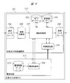
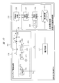
- FIG. 2 is a block diagram illustrating an example of a configuration of the autonomous traveling control ECU 201 included in the in-vehicle system 10 of FIG.
- the autonomous traveling control ECU 201 includes an autonomous traveling control logic unit 210 and a power supply circuit 211.
- the power supply circuit 211 supplies power to the reconfiguration circuit 209.
- the autonomous traveling control logic unit 210 power is supplied to each functional block other than the reconfiguration circuit 209 by a power circuit (not shown).
- the autonomous running control logic unit 210 includes communication interfaces 204 and 208 (hereinafter, collectively referred to as “communication interface 204”), an information collection unit 205, a power supply control unit 206, a function control unit 207, A reconfiguration circuit 209, a mode database 202, a processing item database 203, and a power control database 212 are included.
- the function control unit 207 holds a circuit database (not shown) to be described later.
- the communication interface 204 is an interface that communicates with a predetermined protocol such as CAN used in an in-vehicle system.
- the autonomous traveling control ECU 201 is connected to another device via the communication interface 204, and transmits and receives data.
- the autonomous traveling control ECU 201 is connected to the camera 101, the radar 102, the host vehicle position sensor 103, the automatic driving button 104, and the wireless communication device 105 via the communication interface 204.
- the autonomous travel control ECU 201 is connected to the auxiliary control ECU 106, the brake control ECU 107, the engine control ECU 108, and the power steering control ECU 109 via the communication interface 208, respectively.
- the information collecting unit 205 collects sensor information from the camera 101, the radar 102, and the vehicle position sensor 103 input from the communication interface 204, and an automatic driving control signal from the automatic driving button 104, and collects sensor information and The automatic operation control signal is periodically transferred to the function control unit 207.
- the information collection unit 205 when the information collection unit 205 receives the update information including the autonomous travel control processing information, the circuit data to be updated, and the power supply control data from the wireless communication device 105, the information collection unit 205 stores the circuit data to be updated in a circuit database (not shown), and 202, the contents of the processing item database 203, and the power control database 212 are updated.
- the wireless communication device 105 may be configured to be provided in the autonomous travel control ECU 201, for example.
- the information collecting unit 205 is connected to each database included in the autonomous traveling control logic unit 210 via a control line (not shown). An example of the update information processing will be described later with reference to FIG.
- the function control unit 207 refers to the mode database 202 based on the mode determination signal such as the sensor information and the automatic driving control signal acquired from the information collecting unit 205, and first, the highway approach mode, the automatic parking mode, or the ECU abnormality The operation mode such as the mode is determined.
- processing information indicating how the reconfiguration circuit 209 performs the arithmetic processing required in the operation mode is determined.
- this processing information means the number of divisions of the circuit area of the reconfigurable circuit 209, circuit data for updating each circuit area, calculation time, and the like. Details of the mode database 202 and the processing item database will be described with reference to FIGS. 3 and 4 to be described later.
- the function control unit 207 changes the reconfiguration circuit 209 based on the processing information described above, and causes the reconfiguration circuit 209 to perform the processing of the operation mode.
- a dotted arrow between the function control unit 207 and the reconfiguration circuit 209 indicates transfer of circuit data for the function control unit 207 to reconfigure a circuit from a circuit database (not shown) and a completion notification thereof.
- a solid line arrow between the function control unit 207 and the reconfiguration circuit 209 indicates a process execution instruction, execution data, and transfer of the execution result.
- the function control unit 207 outputs a control command such as a brake and a driving force through the communication interface 208 based on the processing result performed by the reconfiguration circuit 209.
- the reconfiguration circuit 209 is a circuit that executes predetermined processing on data, and is configured by hardware such as an FPGA that can change the circuit configuration.
- the function control unit 207 changes the circuit configuration in accordance with the processing information described above, and executes predetermined processing.
- the power supply control unit 206 acquires mode information from the function control unit 207 and an internal timer value managed by the function control unit 207.
- the internal timer value here is a counter value incremented by the internal clock.
- the power control unit 206 synchronizes by updating the internal timer value of the power control unit 206 based on the acquired internal timer value.
- the power control database 212 stores information related to a power control schedule such as a control signal to the power circuit 211 and timing.
- the power control unit 206 performs power control so as to increase or decrease the current supplied from the power circuit 211 based on the power control database 212 and the above-described internal timer value.
- the power supply control database 212 will be described later with reference to FIG. Details of the power supply control process will be described later with reference to FIGS. 4 and 5.
- the power supply circuit dedicated to the reconfiguration circuit 209 has been described here, the power supply circuit 211 may be a power supply circuit that supplies power to the entire autonomous traveling control logic unit 210.
- Each function unit of the autonomous traveling control logic unit 210 that is, the information collecting unit 205, the function control unit 207, and the power source control unit 206 is a program executed by the autonomous traveling control logic unit 210 or a logic circuit that performs a predetermined operation, for example, Configured by FPGA. From the viewpoint of functional safety of automatic driving, each functional unit of the autonomous traveling control logic unit 210 may be configured by a processor having a plurality of cores adopting a lockstep method.
- the autonomous traveling control logic unit 210 may be physically configured on one electronic control device, or logically or physically on a plurality of electronic control devices.
- the program of each functional unit described above may operate in a separate thread on the same electronic control device, or may operate on a virtual electronic control device constructed on the resources of a plurality of electronic control devices. Good.
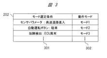
- FIG. 3 is an explanatory diagram of the mode database 202 included in the autonomous traveling control logic unit 210 of FIG.
- the mode database 202 is referred to by the function control unit 207 in FIG. 2 and associates information acquired from the information collection unit 205 with an operation mode to be selected.
- the mode database 202 has a mode selection condition 301 for selecting an operation mode based on information acquired from the information collection unit 205 and an operation mode 302 selected by the mode selection condition 301.
- the mode selection condition 301 is determined to have entered the expressway based on parameter information of external recognition sensors such as the camera 101, the radar 102, and the own vehicle position sensor 103 shown in FIG.
- the case may be the first mode selection condition, and in the operation mode 302, the first operation mode may be determined as the mode 1.
- the mode selection condition 301 the case where the control signal for automatically parking by the automatic operation button 104 in FIG. 1 is received as the second mode selection condition.
- the second operation mode is set to mode 2. You may judge.
- the third operation mode may be determined as mode 3.
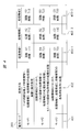
- FIG. 4 is an explanatory diagram of the processing item database 203 included in the autonomous traveling control logic unit 210 of FIG.
- the processing item database 203 is referred to by the function control unit 207 in FIG. 2 and associates the operation mode 302 with the processing content of the corresponding mode.
- This processing item database 203 describes, for each operation mode 401, processing method 402 and processing information 1 (403-1) to processing information 3 (403-3) (when processing information is collectively referred to as “processing information 403”). )).
- the processing method 402 designates the order of single or plural processing to be performed, the circuit reconfiguration procedure, and the like.
- the processing information 403 is processing information specified by the processing method 402.
- the operation mode 401 is mode 1
- one circuit area is provided on the reconfiguration circuit 209 in FIG. 2, and the processing information 1 (403-1) is processed on the circuit area.
- the processing method 402 holds that processing (403-2) and processing information 3 (403-3) are processed in order.
- the circuit data A1 for executing the first processing in mode 1 and the processing time T11 may be held as processing information 1 (403-1).
- the processing time T13 may be held as processing information 3 (403-3).
- the first process in mode 1 is a sensing process
- the second process in mode 1 is a behavior prediction process for a vehicle or a pedestrian
- the third process in mode 1 is a travel route calculation of the vehicle. It is good also as processing.
- the circuit area is divided into two, and processing of processing information 1 (403-1) and processing information 2 (403-2) is sequentially processed in one area.
- the processing method 402 may hold that the processing of the processing information 3 (403-3) is performed in the other area.
- the circuit data B1 to B3 for executing the first to third processes of the mode 2 and the respective processing times T21 to T23 are held as the processing information 403. May be.
- any one of the first to third processes in mode 2 may be an empty parking space search process.
- the operation mode 401 is mode 3
- the circuit area is divided into three and each of processing information 1 (403-1), processing information 2 (403-2), and processing information 3 (403-3) Processing in parallel may be held as the processing method 402.
- the circuit data C1 to C3 for executing the first to third processes of the mode 3 and the respective processing times T31 to T33 are held as the processing information 403. May be.
- any of the first to third processes in mode 3 may be a track securing process for safely stopping the vehicle.
- processing information 403 Although an example in which three pieces of information (processing information 1 (403-1) to processing information 3 (403-3)) are held as the processing information 403 is shown here, four or more pieces of information may be held. Good.
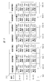
- FIG. 5 is an explanatory diagram of the power control database 212 included in the autonomous driving control logic unit 210 of FIG.
- the power control database 212 stores information related to a power control schedule such as a control signal and timing to the power circuit 211.
- the power supply control database 212 is referred to by the power supply control unit 206 of FIG. 2, and the control information 0 (503-0) to the control information 6 (503-6) (power supply) which are the power control contents of the operation mode 501 and the operation mode 501.
- control information 503 When the control information is collectively referred to, it is described as “power control information 503”).
- the timer value TA0 is a timer value that takes into account the timing at which the connection circuit to the interface with the function control unit 207 in FIG.
- the load current value IA0 is a load current value of the reconfiguration circuit 209 during writing.
- a timer value TA1 that considers the timing to start writing circuit data A1 for executing the first process of mode 1 to the reconfiguration circuit 209, a load current value IA1 of the reconfiguration circuit 209 being written, and a processing time PA1 are obtained. It may be held as control information 1 (503-1).
- the timer value TA2 in consideration of the timing at which the first process of mode 1 is started, the load current value IA2 of the reconfiguration circuit 209 that is executing the first process, and the process You may make it hold
- the timer value TA3 in consideration of the timing to start writing the circuit data A2 for executing the second process of mode 1 to the reconfiguration circuit 209, the load current of the reconfiguration circuit 209 being written
- the value IA3 and the processing time PA3 may be held.
- the timer value TA4 in consideration of the timing at which the second process of mode 1 is started, the load current value IA4 of the reconfiguration circuit 209 that is executing the second process, and the process You may make it hold
- the timer value TA5 in consideration of the timing to start writing the circuit data A3 for executing the third process of mode 1 to the reconfiguration circuit 209, the load current of the reconfiguration circuit 209 being written
- the value IA5 and the processing time PA5 may be held.
- the control information 6 (503-6) includes a timer value TA6 in consideration of the timing at which the third process of mode 1 is started, the load current value IA6 of the reconfiguration circuit 209 that is executing the third process, and the process You may make it hold
- Each load current value may hold, for example, a temporal average value of the load current.
- the power supply circuit 211 in FIG. 2 supplies power only to the reconfiguration circuit 209, but even if the power supply circuit 211 is configured to supply power to the entire autonomous traveling control logic unit 210. Good. In that case, the load current value of the entire autonomous traveling control logic unit 210 is stored in the power supply control database 212.
- the timer value is, for example, a counter value incremented by an internal clock, and is managed by the function control unit 207 in FIG. 2 and used for synchronization with the power supply control unit 206.
- This timer value takes into account the signal delay between the function control unit 207 and the power supply control unit 206 and the control delay from when the power supply control unit 206 starts the power supply control process until the supply current of the power supply circuit 211 increases or decreases.
- the supply current of the power supply circuit 211 is adjusted so as to increase or decrease.
- This power supply control database 212 may store each numerical value based on an actual measurement value or a simulation value before operating as an in-vehicle system, or a processing item database acquired by the power supply control unit 206 from the function control unit 207. It may be created and stored based on each piece of information 203.
- the power supply control information 503 may include a voltage value, a current value, or a control code for controlling the supply current of the power supply circuit 211.
- FIG. 6 is a flowchart showing an example of the power control process in the power control unit 206 of FIG.
- the power control database 212 is created and stored in advance, and the power control unit 206 manages the processing order using the internal control ID.
- the internal control ID indicates a number of control information 0 to 6 in the power supply control information 503 in FIG. Further, description will be made assuming that the function control unit 207 and the power supply control unit 206 in FIG. 2 are each provided with an internal timer.
- step S600 when the power supply control unit 206 starts the power supply control process (step S600), the power supply control unit 206 acquires mode information and a timer value from the function control unit 207 before the reconfiguration circuit calculation is started. The timer value is updated (step S601).
- step S601 the power supply control unit 206 determines whether or not the operation mode is the same as the previous mode value (step S602). If it is determined in step S602 that the operation mode is different from the previous mode value (NO), the power supply control unit 206 sets the internal control ID to 0 (step S603).
- the power supply control unit 206 sets the internal control ID to 1 (step S604). This determines whether or not the process of writing the connection circuit to the interface with the function control unit 207 in the reconfiguration circuit 209 is based on whether or not the operation mode is different from the previous one.
- the ID information of the connection circuit described above may be obtained from the function control unit 207 to determine whether or not it is the same as the previous time.
- the power supply control unit 206 refers to the power supply control database 212 and waits until the timer value indicated by the internal control ID matches the internal timer value of the power supply control unit 206. (Step S605).
- step S605 If it is determined in step S605 that the timer values match (YES), the load current value and processing time indicated by the internal control ID are transmitted to the power supply circuit 211 as a power supply control instruction (step S606).
- the power supply circuit 211 supplies a reference current value until receiving a power supply control instruction.
- the power supply circuit 211 increases or decreases the supply current so that the load current value indicated by the internal control ID is obtained.
- the reference current value is supplied again.
- the reference current value may be set in consideration of the leakage current when the supply target is only the reconfiguration circuit 209. In the case of supplying power to the entire autonomous traveling control logic unit 210, it may be set in consideration of a load current other than that of the reconfiguration circuit 209.
- the power supply control unit 206 determines whether or not there is a next process (step S607). Whether or not there is the next processing can be determined by the power supply control unit 206 from the power supply control database 212 of FIG.
- step S607 If it is determined in step S607 that the next process is present (YES), the power supply control unit 206 increments the internal process ID (step S608) and returns to the process in step S605 to prepare for the next process.
- step S607 If it is determined in step S607 that there is no next process (NO), the power supply control unit 206 ends the power supply control process (step S609).
- FIG. 7 is a sequence diagram showing an example of the power control process in the power control unit 206 of FIG.
- FIG. 7 illustrates an example in which the operation mode 501 of the power supply control database 212 described above with reference to FIG.
- the power control database 212 is created and stored in advance.
- the function control unit 207 acquires mode information from the mode database 202 and confirms whether or not the mode is switched. Further, an internal timer value managed by the function control unit 207 is acquired (step S700). Here, an example in which the mode is switched is shown.
- the function control unit 207 sends the mode information and the timer value to the power supply control unit 206 (step S701).
- the power control unit 206 updates the internal timer value of the power control unit 206 based on this timer value (step S702).
- control information 0 (503-0) relating to the reconfiguration of the connection circuit to the interface with the function control unit 207 held in the power control database 212 the timer value and the internal timer value of the power control unit 206 are Are matched, the load current value and the processing time are transmitted to the power supply circuit 211 as a power supply control instruction (step S704).
- the power supply circuit 211 increases or decreases the supply current to the reconfiguration circuit 209 from the reference current value so as to become the load current value indicated by the internal control ID. (Step S705).
- the function control unit 207 writes connection circuit data with the interface with the function control unit 207 in the reconfiguration circuit 209 slightly after the start of the current control in the process of step S705, for example, about 1 millisecond or less (step S707). ).
- the reconfiguration circuit 209 reconfigures the interface connection circuit (step S708), and notifies the function control unit 207 of the completion of writing (step S709). Then, the power supply control unit 206 refers to the control information 1 (503-1) relating to the reconfiguration of the circuit data A1 held in the power supply control database 212, and determines the timer value and the internal timer value of the power supply control unit 206. Are matched, the load current value and the processing time are transmitted to the power supply circuit 211 as a power supply control instruction (step S710).
- the power supply circuit 211 increases or decreases the supply current to the reconfiguration circuit 209 from the reference current value so as to become the load current value indicated by the internal control ID. (Step S711).
- the function control unit 207 writes the data of the circuit A1 in the reconfiguration circuit 209 slightly later than the current control start by the processing of S711 (step S713).
- the reconfiguration circuit 209 reconfigures the circuit A1 (step S714), and notifies the function controller 207 of the completion of writing (step S715).
- the power supply control unit 206 refers to the control information 2 (503-2) related to the first process stored in the power supply control database 212, and determines the timer value and the internal timer value of the power supply control unit 206. Are matched, the load current value and the processing time are transmitted to the power supply circuit 211 as a power supply control instruction (step S716).
- the power supply circuit 211 increases or decreases the supply current to the reconfiguration circuit 209 from the reference current value to the load current value indicated by the internal control ID, and again when the processing time indicated by the internal control ID ends.
- the reference current value is restored (step S717).
- the function control unit 207 notifies the reconfiguration circuit 209 of the execution instruction of the first process slightly after the start of the current control of the process of step S717 (step S719).
- the reconfiguration circuit 209 executes the calculation of the first process (step S720), and notifies the function control unit 207 of the completion of the execution together with the calculation result, in other words, the process result (step S721).
- the function control unit 207 may hold the calculation result of the first process and use it for the calculation of the subsequent process.
- step S722 confirms the presence or absence of the next process.
- the operation mode 501 is mode 1 and the second process is the next process.
- the function control unit 207 transmits a power control continuation instruction to the power control unit 206 (step S723).
- the power control unit 206 refers to the control information 3 (503-3) relating to the reconfiguration of the circuit data A2 held in the power control database 212, and the timer value matches the internal timer value of the power control unit 206. Then, the load current value and the processing time are transmitted to the power supply circuit 211 as a power supply control instruction (step S724).
- circuit data A2 and second processing using the same circuit data A3 and third processing using the same are performed.
- the function control unit 207 confirms the presence / absence of the next process (step S753).
- the operation mode 501 is mode 1 and there is no next processing
- an end instruction is sent to the power supply control unit 206 (step S754), and the power supply control unit 206 receives it and waits for reception (step S755).
- the sequence of the power control process is completed.
- the function control unit 207 and the power supply control unit 206 have been described as including internal timers, but may include a common internal timer.
- the autonomous traveling control logic unit 210 performs processing periodically based on the collected sensor information, automatic driving control signals, and the like. Therefore, as described above, it is not always necessary for the power supply control unit 206 to acquire each piece of information from the function control unit 207 every period.
- a delay may be given to the start time of the reconfiguration processing or arithmetic processing of the reconfiguration circuit 209.
- the power supply circuit 211 also supplies power other than the reconfiguration circuit 209
- calculation may be performed while avoiding a section in which the load fluctuation of the reconfiguration circuit 209 occurs with respect to the blocks of other autonomous traveling control logic units.
- the computation in the same section may be made redundant.
- FIG. 8 is a sequence diagram showing an example of operation mode expansion in the in-vehicle system 10 of FIG.
- FIG. 8 shows an example of adding an operation mode of automatic operation via a wireless network by OTA (Over-The-Air) from a server on the cloud, for example.
- OTA Over-The-Air
- step S1100 when an operation mode addition instruction is set in the server (step S1100), information on the operation mode to be added is transferred to the wireless communication device 105 of the in-vehicle system (S1101).
- the information regarding the operation mode includes, for example, the contents of the mode database 202, the processing item database 203, and the power control database 212, and circuit data of the operation mode to be added.
- the wireless communication device 105 transfers the received additional information to the autonomous travel control logic unit 210 (step S1102). Then, the autonomous traveling control logic unit 210 stores the circuit data in the circuit database (step S1103).
- the autonomous traveling control logic unit 210 sets the operation mode 501 and control information 503 to be added to the power supply control database 212 (step S1104). Further, the autonomous traveling control logic unit 210 sets the operation mode 401 to be added, the processing method 402, and the processing information 403 in the processing item database 203 (step S1105).
- the autonomous traveling control logic unit 210 adds the operation mode selection condition 301 and the operation mode 302 to the mode database 202 (S1106) and completes the processing.
- circuit data and processing method used in the added operation mode are introduced to the autonomous driving control unit without affecting the operating mode in use. be able to.
- the power supply control unit 206 obtains information on the reconfiguration and calculation schedule from the function control unit 207 that controls the reconfiguration and calculation of the reconfiguration circuit 209, and the load caused by the reconfiguration and calculation of the reconfiguration circuit 209.
- the power supply circuit 211 can be controlled to increase or decrease the supply current to the reconstruction circuit 209 prior to the fluctuation.
- the transient increase and decrease of the output voltage of the power supply circuit 211 can be reduced, and the highly reliable autonomous traveling control ECU 201 can be provided at low cost and in a small area.
- FIG. 9 is a block diagram showing another example of the autonomous traveling control ECU 201 in FIG.
- the autonomous traveling control ECU 201 includes an autonomous traveling control logic unit 210 and a power supply circuit 211.
- the power circuit 211 supplies power to the reconfiguration circuit 209, and power supply to the autonomous traveling control logic unit 210 other than the reconfiguration circuit 209 is performed by a power circuit (not shown).
- the autonomous traveling control ECU 201 in FIG. 9 is significantly different from the autonomous traveling control ECU 201 in FIG. 2 in that the power control unit 206 and the power control database 212 are included in the power circuit 211 instead of the autonomous traveling control logic unit 210.
- Basic processing and control may be considered to be the same as described above with reference to FIG.
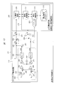
- FIG. 10 is an explanatory diagram showing an example of a configuration in the autonomous traveling control ECU 201 according to the second embodiment.
- the autonomous traveling control ECU 201 includes an autonomous traveling control logic unit 210, a switching power supply circuit 275, and a power supply circuit 277.
- the autonomous traveling control logic unit 210 includes a reconfiguration circuit 209 and a non-reconfiguration circuit 276.
- the non-reconfigurable circuit 276 includes a function control unit 207, a power control unit 206, a power control database 212, and a D / A (Digital / Analog) converter 263.
- the function control unit 207 holds a circuit database (not shown).
- the switching power supply circuit 275 supplies power to the reconfiguration circuit 209, and the power supply circuit 277 supplies power to the non-reconfiguration circuit 276.
- the autonomous travel control ECU 201 has a plurality of communication interfaces, an information collection unit, a mode database, and a processing item database, as in FIG. 1 of the first embodiment.
- the power supply control unit 206 acquires mode information from the function control unit 207 and an internal timer value managed by the function control unit 207. Further, the power control unit 206 achieves synchronization by updating the internal timer value of the power control unit 206 based on the acquired internal timer value.
- the power supply control database 212 stores information related to a power supply control schedule such as a control signal to the switching power supply circuit 275 and timing.
- the power supply control unit 206 performs power supply control so as to increase or decrease the supply current of the switching power supply circuit 275 based on the power supply control database 212 and the above-described internal timer value.
- the D / A converter 263 is used to convert the power supply control signal from a digital value to an analog value and transmit it to the switching power supply circuit 275. Details of the power supply control database 212 will be described later with reference to FIG.
- the switching power supply circuit 275 includes an inductor current control unit 274, switches 267 and 268, an inductor 265, and a capacitor 264.
- PWM Pulse Width Modulation
- the inductor current control unit 274 increases or decreases the inductor current IL flowing through the inductor 265 by performing ON / OFF control of the switches 267 and 268. Since the output voltage Vo1 generated by the output current Io1 flowing through the reconfiguration circuit 209 has a large ripple due to the fluctuation of the inductor current IL, the output voltage Vo1 is smoothed by the capacitor 264 to a voltage close to DC.
- the inductor current control unit 274 includes a switch driver 269, a comparator 270, a triangular wave generator 271, an error detector 272, and an adder 273.
- the reference voltage VREF1 and the observed output voltage Vo1 are input to the error detector 272, and the difference between the two input is output from the error detector 272. The difference is input to the comparator 270 together with the output of the triangular wave generator 271.
- the comparator 270 outputs a PWM signal corresponding to the above-described difference.
- the switch driver 269 performs ON / OFF control of the switches 267 and 268 in accordance with the PWM signal, and adjusts the inductor current IL.
- the switching power supply circuit 275 operates so as to maintain the output voltage Vo1 constant by such a feedback system, and steps down the input voltage Vin.
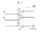
- FIG. 11 is a schematic diagram of changes in the inductor current waveform and output voltage to show the effect of power control by the power control unit 206 in FIG.
- the output voltage 805 has a large ⁇ V1 in accordance with the insufficient charge amount (corresponding to the area ⁇ in FIG. 11). A voltage drop occurs.
- the power supply control signal VPLS is a voltage pulse signal that is added to VREF1 via the adder 273 before the load fluctuation timing.
- the inductor current IL can be controlled to increase or decrease before the timing when the load current 801 changes suddenly.
- the areas of ⁇ 1 and ⁇ 2 can be matched as in the inductor current 803 in FIG.
- FIG. 12 is an explanatory diagram of the power supply control database 212 included in the autonomous traveling control ECU 201 of FIG.
- the power supply control database 212 stores information related to a power supply control schedule such as control signals and timing to the switching power supply circuit 275 in FIG.
- the power supply control database 212 is referred to by the power supply control unit 206, and control information 0 (513-0) to control information 6 (513-6) (generic name of power supply control information) which are the power control contents of the operation mode 511 and the corresponding mode. In this case, it is described as “power control information 513”.
- the control information 0 (513-0) includes the timer value TA01, the power supply control signal voltage value VA01, the pulse width time PA01, the timer value TA02, and the power supply control signal voltage value. VA02 and pulse width time PA02 may be held.
- the timer value TA01 is a timer value in consideration of the timing at which the connection circuit to the interface with the function control unit 207 starts to be written in the reconfiguration circuit 209.
- the timer value TA02 is a timer value that takes into account the timing at which the connection circuit is written to the reconfiguration circuit 209.
- the timer value TA11 in consideration of the timing to start writing the circuit data A1 for executing the first processing of mode 1 to the reconfiguration circuit 209, the voltage value VA11 of the power control signal
- the pulse width time PA11, the timer value TA12 in consideration of the timing to finish writing the circuit data A1 to the reconfiguration circuit 209, the voltage value VA12 of the power supply control signal, and the pulse width time PA12 may be held.
- the timer value TA21, the power control signal voltage value VA21, the pulse width time PA21, and the first process are executed in consideration of the timing at which the first process of the mode 1 is started.
- the timer value TA22 in consideration of the end timing, the voltage value VA22 of the power supply control signal, and the pulse width time PA22 may be held.
- the timer value TA31, the voltage value VA31 of the power supply control signal, the pulse width in consideration of the timing to start writing the circuit data A2 for executing the second process of mode 1 to the reconfiguration circuit 209
- the timer value TA32, the voltage value VA32 of the power supply control signal, and the pulse width time PA32 may be held in consideration of the time PA31, the timing at which the circuit data A2 is written to the reconfiguration circuit 209.
- the timer value TA41, the voltage value VA41 of the power supply control signal, the pulse width time PA41, and the second process are executed in consideration of the timing at which the second process of the mode 1 is started.
- the timer value TA42 in consideration of the end timing, the voltage value VA42 of the power supply control signal, and the pulse width time PA42 may be held as the control information 4 (513-4).
- the timer value TA51, the voltage value VA51 of the power supply control signal, the pulse width in consideration of the timing to start writing the circuit data A3 for executing the third process of mode 1 to the reconfiguration circuit 209
- the timer value TA52, the voltage value VA52 of the power supply control signal, and the pulse width time PA52 may be held in consideration of the time PA51, the timing at which the circuit data A3 is written to the reconfiguration circuit 209.
- the timer value TA61, the voltage value VA61 of the power supply control signal, the pulse width time PA61, and the third process are executed in consideration of the timing at which the third process of mode 1 is started.
- the timer value TA62, the voltage value VA62 of the power supply control signal, and the pulse width time PA62 taking into account the end timing may be held.
- the timer value is a counter value incremented by an internal clock, is managed by the function control unit 207, and is used for synchronization with the power supply control unit 206.
- This timer value is a signal delay between the function control unit 207 and the power supply control unit 206 or a control delay from when the power supply control unit 206 starts the power supply control process until the supply current of the switching power supply circuit 275 increases or decreases.
- the supply current of the switching power supply circuit 275 is adjusted to increase or decrease before the load current of the reconfiguration circuit 209 fluctuates.
- the power supply control database 212 may store each numerical value based on an actual measurement value or a simulation value before operating as an in-vehicle system, or may be a processing item database acquired by the power supply control unit 206 from the function control unit 207. You may create and store based on each information.
- the voltage pulse signal is added to the reference voltage VREF1 as the power supply control signal has been described, but it may be added to the output voltage value input to the error detector 272. Further, a power supply control signal that temporarily increases the response speed of the feedback loop of the switching power supply circuit 275 may be used so as to cope with a sudden change in the load current.
- the gain of the comparator 270 may be increased, or the frequency of the triangular wave generator 271 may be increased. Further, instead of controlling the switching power supply circuit by the PWM control method, a hysteresis control method may be used.
- an observation unit for monitoring the power supply voltage supplied to the reconfiguration circuit 209 is provided, for example, with the voltage value monitored by the power supply control unit 206 and the set voltage initially set in the power supply control database 212. It may be compared with a certain control voltage, and the power supply control database 212 may be updated according to the error between the two.
- the voltage may be divided by a high resistance and observed by the power supply control unit 206 through an operational amplifier and an A / D (Analog / Digital) converter.
- a / D Analog / Digital
- the value of (control voltage value ⁇ observed voltage value) may be added to the control voltage value of the power supply control database 212.
- a correction function using (control voltage value ⁇ observed voltage value) as an input value may be incorporated in the power supply control unit 206 in advance, and the power supply control database 212 may be updated based on the output value.
- FIG. 13 is an explanatory view showing another configuration example of the autonomous traveling control ECU 201 of FIG.
- a switching power supply circuit 275 shown in FIG. 13 is a single-inductor-two-output SIMO (Single Inductor Multi-Output) power supply circuit, and supplies power to the reconfiguration circuit 209 and the non-reconfiguration circuit 276. Since the SIMO power supply circuit has a plurality of outputs with one inductor, it is a technology that can contribute to cost reduction and area saving.
- SIMO Single Inductor Multi-Output
- the switching power supply circuit 275 includes an inductor current control unit 298, switches 283, 284, 286, 287, an inductor 285, and capacitors 281, 282, as shown.
- the inductor current control unit 298 increases or decreases the inductor current IL flowing through the inductor 285 by performing ON / OFF control of the switches 286 and 287.
- the output destination of the power supply voltage is changed to the reconfiguration circuit 209 or the non-reconfiguration circuit 276 by performing ON / OFF control of the switches 283 and 284.
- These switches 283 and 284 and the inductor current control unit 298 constitute an output switching unit.
- the output voltage Vo1 generated by the output current Io1 flowing through the reconfiguration circuit 209 has a large ripple due to the fluctuation of the inductor current IL, the output voltage Vo1 is smoothed by using the capacitor 281 to be a voltage close to DC.
- the inductor current control unit 298 includes switch drivers 288 and 289, comparators 290 and 291, a triangular wave generator 292, error detectors 293 and 294, adders 295, 296 and 297 and the like.
- the power control signal VPLS sent from the power control unit 206 through the D / A converter 263 is added to the reference voltage VREF1 by the adder 296.
- the output voltage Vo1 and the output voltage Vo2 added by the adder 295 are added. These added voltages are input to the error detector 293, and a difference between these voltages is output from the error detector 293.
- the difference is input to the comparator 290 together with the output of the triangular wave output device 292.
- the comparator 290 outputs a PWM signal corresponding to the above difference.
- the switch driver 288 performs ON / OFF control of the switches 286 and 287 according to the PWM signal, and adjusts the inductor current IL.
- the power supply control signal VPLS is also added to the reference voltage VREF2 by the adder 296, and is input to the error detector 294 together with the observed output voltage Vo2, and the difference between the two is output from the error detector 294.
- the difference is input to the comparator 291 together with the output of the triangular wave output device 292.
- the comparator 291 outputs a PWM signal corresponding to the above difference.
- the switch driver 289 performs ON / OFF control of the switches 283 and 284 in accordance with the PWM signal, and adjusts the output destination.
- the switching power supply circuit 275 operates to maintain the output voltage Vo1 and the output voltage Vo2 constant by such a feedback system, and steps down the input voltage Vin.
- the power supply control signal VPLS is a voltage pulse signal to be added to the reference voltages VREF1 and VREF2 before the timing of this load change, and is stored in advance in the control information database 212, for example.
- the inductor current IL can be controlled to increase or decrease before the timing when the load current suddenly changes, and the voltage transient fluctuation of the output voltage can be reduced.
- the power supply circuit can be controlled to increase or decrease the supply current to the reconfiguration circuit 209 prior to the load fluctuation caused by the reconfiguration and calculation of the reconfiguration circuit 209 using a simple analog circuit.
- the transient increase and decrease of the output voltage of the switching power supply circuit 275 can be reduced, and the highly reliable autonomous traveling control ECU 201 can be provided at low cost and in a small area.
- a part of the configuration of one embodiment can be replaced with the configuration of another embodiment, and the configuration of another embodiment can be added to the configuration of one embodiment. .
- each of the above-described configurations, functions, processing units, processing means, and the like may be realized by hardware by designing a part or all of them with, for example, an integrated circuit.
- Each of the above-described configurations, functions, and the like may be realized by software by interpreting and executing a program that realizes each function by the processor.
- Information such as programs, tables, and files for realizing each function can be stored in a recording device such as a memory, a hard disk, an SSD (Solid State Drive), or a recording medium such as an IC card, an SD card, or a DVD.
- control lines and information lines indicate what is considered necessary for the explanation, and not all the control lines and information lines on the product are necessarily shown. Actually, it may be considered that almost all the components are connected to each other.
Landscapes
- Engineering & Computer Science (AREA)
- Automation & Control Theory (AREA)
- Mechanical Engineering (AREA)
- Theoretical Computer Science (AREA)
- General Physics & Mathematics (AREA)
- Physics & Mathematics (AREA)
- Transportation (AREA)
- General Engineering & Computer Science (AREA)
- Human Computer Interaction (AREA)
- Electromagnetism (AREA)
- Radar, Positioning & Navigation (AREA)
- Combustion & Propulsion (AREA)
- Chemical & Material Sciences (AREA)
- Power Engineering (AREA)
- Traffic Control Systems (AREA)
- Power Sources (AREA)
- Dc-Dc Converters (AREA)
Abstract
La présente invention réduit les augmentations/réductions transitoires de l'énergie devant être fournie à un circuit reconfigurable, ce dernier étant un circuit logique dont la configuration de circuit est modifiable. Une ECU de commande de déplacement autonome (201) possède un circuit reconfigurable (209), une unité de commande fonctionnelle (207), un circuit d'alimentation (211) et une unité de commande d'alimentation (206). Le circuit reconfigurable (209) est un circuit logique qui peut être reconfiguré. L'unité de commande fonctionnelle (207) détermine le mode de fonctionnement du circuit reconfigurable (209) sur la base d'un signal de détermination de mode et commande la reconfiguration du circuit reconfigurable (209) sur la base du résultat de détermination. Le circuit d'alimentation électrique (211) fournit de l'énergie au circuit reconfigurable (209). L'unité de commande d'alimentation (206) commande le circuit d'alimentation. L'unité de commande d'alimentation (206) commande le courant de charge généré par le circuit d'alimentation (211) avant qu'une charge du circuit reconfigurable (209) ne fluctue sur la base d'informations de commande d'alimentation qui sont des informations permettant de commander le circuit d'alimentation (211).
Priority Applications (3)
| Application Number | Priority Date | Filing Date | Title |
|---|---|---|---|
| US16/463,284 US11235780B2 (en) | 2016-11-28 | 2017-09-12 | Electronic control device, in-vehicle system, and power supply control method |
| CN201780071168.3A CN110023167B (zh) | 2016-11-28 | 2017-09-12 | 电子控制装置、车载系统以及电源控制方法 |
| DE112017005279.3T DE112017005279T5 (de) | 2016-11-28 | 2017-09-12 | Elektronische Steuervorrichtung, fahrzeuginternes System und Leistungsversorgungssteuerverfahren |
Applications Claiming Priority (2)
| Application Number | Priority Date | Filing Date | Title |
|---|---|---|---|
| JP2016230386A JP6618455B2 (ja) | 2016-11-28 | 2016-11-28 | 電子制御装置、車載システム、および電源制御方法 |
| JP2016-230386 | 2016-11-28 |
Publications (1)
| Publication Number | Publication Date |
|---|---|
| WO2018096767A1 true WO2018096767A1 (fr) | 2018-05-31 |
Family
ID=62195890
Family Applications (1)
| Application Number | Title | Priority Date | Filing Date |
|---|---|---|---|
| PCT/JP2017/032772 WO2018096767A1 (fr) | 2016-11-28 | 2017-09-12 | Appareil de commande électronique, système à bord d'un véhicule et procédé de commande d'alimentation |
Country Status (5)
| Country | Link |
|---|---|
| US (1) | US11235780B2 (fr) |
| JP (1) | JP6618455B2 (fr) |
| CN (1) | CN110023167B (fr) |
| DE (1) | DE112017005279T5 (fr) |
| WO (1) | WO2018096767A1 (fr) |
Cited By (1)
| Publication number | Priority date | Publication date | Assignee | Title |
|---|---|---|---|---|
| WO2019235076A1 (fr) * | 2018-06-06 | 2019-12-12 | 日立オートモティブシステムズ株式会社 | Dispositif de commande électronique |
Families Citing this family (2)
| Publication number | Priority date | Publication date | Assignee | Title |
|---|---|---|---|---|
| US10996730B2 (en) * | 2018-03-15 | 2021-05-04 | Ricoh Company, Ltd. | Electronic device including power supply and method to be executed by electronic device |
| US11435438B2 (en) * | 2019-12-30 | 2022-09-06 | Woven Planet North America, Inc. | Dynamic sparse radar array for scenarios |
Citations (7)
| Publication number | Priority date | Publication date | Assignee | Title |
|---|---|---|---|---|
| JP2006060918A (ja) * | 2004-08-20 | 2006-03-02 | Renesas Technology Corp | 電子装置 |
| JP2010151619A (ja) * | 2008-12-25 | 2010-07-08 | Equos Research Co Ltd | 制御装置 |
| JP2010282563A (ja) * | 2009-06-08 | 2010-12-16 | Toyota Motor Corp | 電子制御ユニット、回路再構築方法 |
| JP2011103725A (ja) * | 2009-11-10 | 2011-05-26 | Fuji Electric Systems Co Ltd | 力率改善型スイッチング電源装置 |
| JP2014046748A (ja) * | 2012-08-30 | 2014-03-17 | Toyota Motor Corp | 車両制御装置 |
| JP2014137797A (ja) * | 2013-01-18 | 2014-07-28 | Canon Inc | 情報処理装置、情報処理装置の制御方法及びプログラム |
| WO2016080452A1 (fr) * | 2014-11-19 | 2016-05-26 | エイディシーテクノロジー株式会社 | Dispositif de commande de conduite autonome |
Family Cites Families (36)
| Publication number | Priority date | Publication date | Assignee | Title |
|---|---|---|---|---|
| US7454643B2 (en) | 2003-04-30 | 2008-11-18 | Marvell World Trade Ltd. | Pre-emptive power supply control system and method |
| JP2005119370A (ja) * | 2003-10-14 | 2005-05-12 | Pacific Ind Co Ltd | タイヤ状態監視装置の送信機 |
| US20090292520A1 (en) * | 2006-07-27 | 2009-11-26 | Drexel University | Solver for hardware based computing |
| JP2008149807A (ja) * | 2006-12-15 | 2008-07-03 | Hitachi Ltd | 車両負荷制御装置 |
| JP4960833B2 (ja) * | 2007-10-31 | 2012-06-27 | パナソニック株式会社 | シングルエンド伝送及び差動伝送の切替えが可能なインタフェース回路 |
| CN101971500A (zh) * | 2007-11-13 | 2011-02-09 | 松下电器产业株式会社 | 可编程设备、设备控制方法及信息处理系统 |
| US8237389B2 (en) * | 2008-11-12 | 2012-08-07 | Irobot Corporation | Multi mode safety control module |
| JP2013082391A (ja) * | 2011-10-12 | 2013-05-09 | Autonetworks Technologies Ltd | 車載用ecu |
| US9665101B1 (en) * | 2012-09-28 | 2017-05-30 | Waymo Llc | Methods and systems for transportation to destinations by a self-driving vehicle |
| JP6034699B2 (ja) * | 2013-01-07 | 2016-11-30 | ルネサスエレクトロニクス株式会社 | 半導体装置及びそのコマンド制御方法 |
| EP2811548B1 (fr) * | 2013-06-07 | 2017-08-09 | Autoliv Development AB | Agencement de déconnexion de module de batterie |
| JP6119475B2 (ja) * | 2013-07-15 | 2017-04-26 | 株式会社ジェイテクト | 車載用モータ制御装置 |
| US9368936B1 (en) * | 2013-09-30 | 2016-06-14 | Google Inc. | Laser diode firing system |
| JPWO2015056530A1 (ja) * | 2013-10-17 | 2017-03-09 | みこらった株式会社 | 自動運転車、自動運転車の盗難防止システム、自動運転車の盗難防止プログラム、端末制御用プログラム、自動運転車のレンタル方法及び自動運転車のカーシェアリング方法 |
| KR102183527B1 (ko) * | 2014-02-07 | 2020-11-26 | 팅크웨어(주) | 전자 장치 및 그의 제어 방법 |
| US9676382B2 (en) * | 2014-04-17 | 2017-06-13 | Palo Alto Research Center Incorporated | Systems and methods for hybrid vehicles with a high degree of hybridization |
| US10178535B2 (en) * | 2014-08-19 | 2019-01-08 | Aeryon Labs Inc. | Secure system for emergency-mode operation, system monitoring and trusted access vehicle location and recovery |
| US10157423B1 (en) * | 2014-11-13 | 2018-12-18 | State Farm Mutual Automobile Insurance Company | Autonomous vehicle operating style and mode monitoring |
| CN105717827A (zh) * | 2014-12-04 | 2016-06-29 | 财团法人资讯工业策进会 | 车辆引擎状态侦测装置及方法与车载电子装置 |
| US9871444B2 (en) * | 2014-12-24 | 2018-01-16 | Texas Instruments Incorporated | Integrated circuit with configurable control and power switches |
| KR101659034B1 (ko) * | 2015-01-20 | 2016-09-23 | 엘지전자 주식회사 | 차량의 주행 모드 전환 장치 및 그 방법 |
| WO2016197068A1 (fr) * | 2015-06-03 | 2016-12-08 | Levant Power Corporation | Procédés et systèmes de commande de mouvement de carrosserie de véhicule et d'expérience d'occupant |
| JP6365469B2 (ja) * | 2015-09-03 | 2018-08-01 | トヨタ自動車株式会社 | 車両の制御装置 |
| US20170072812A1 (en) * | 2015-09-16 | 2017-03-16 | Qualcomm Incorporated | Battery Management Systems for Autonomous Vehicles |
| US9802661B1 (en) * | 2015-11-04 | 2017-10-31 | Zoox, Inc. | Quadrant configuration of robotic vehicles |
| US9958864B2 (en) * | 2015-11-04 | 2018-05-01 | Zoox, Inc. | Coordination of dispatching and maintaining fleet of autonomous vehicles |
| KR101788183B1 (ko) * | 2015-12-28 | 2017-10-20 | 현대자동차주식회사 | 차량 및 그 제어방법 |
| US10894519B2 (en) * | 2015-12-28 | 2021-01-19 | Rohm Co., Ltd. | Vehicle switch control device and switch state detection method |
| KR102464926B1 (ko) * | 2016-02-11 | 2022-11-08 | 삼성전자주식회사 | 운송 기기를 제어하는 제어 장치 및 이의 운송 기기 제어 방법 |
| CN109074040A (zh) * | 2016-05-30 | 2018-12-21 | 深圳市大疆创新科技有限公司 | 基于操作参数的飞行限制 |
| CN109195827B (zh) * | 2016-05-31 | 2022-07-26 | 福特全球技术公司 | 对于电动车辆的移动充电的系统 |
| US10025899B2 (en) * | 2016-06-17 | 2018-07-17 | Toyota Motor Engineering & Manufacturing North America, Inc. | Deactivating or disabling various vehicle systems and/or components when vehicle operates in an autonomous mode |
| DE112017003497B4 (de) * | 2016-07-11 | 2020-12-03 | Groove X, Inc. | Selbständig agierender Roboter mit gesteuerter Aktivitätsmenge |
| WO2018011394A2 (fr) * | 2016-07-15 | 2018-01-18 | Innovative Dragon Ltd. | Système de transport, véhicule automoteur et procédé de commande d'un système de transport |
| US10071675B2 (en) * | 2016-08-03 | 2018-09-11 | Ford Global Technologies, Llc | Autonomous vehicle headlight deactivation |
| US10216190B2 (en) * | 2016-09-20 | 2019-02-26 | International Business Machines Corporation | Managing autonomous vehicles needing energy replenishment |
-
2016
- 2016-11-28 JP JP2016230386A patent/JP6618455B2/ja active Active
-
2017
- 2017-09-12 WO PCT/JP2017/032772 patent/WO2018096767A1/fr active Application Filing
- 2017-09-12 DE DE112017005279.3T patent/DE112017005279T5/de active Pending
- 2017-09-12 CN CN201780071168.3A patent/CN110023167B/zh active Active
- 2017-09-12 US US16/463,284 patent/US11235780B2/en active Active
Patent Citations (7)
| Publication number | Priority date | Publication date | Assignee | Title |
|---|---|---|---|---|
| JP2006060918A (ja) * | 2004-08-20 | 2006-03-02 | Renesas Technology Corp | 電子装置 |
| JP2010151619A (ja) * | 2008-12-25 | 2010-07-08 | Equos Research Co Ltd | 制御装置 |
| JP2010282563A (ja) * | 2009-06-08 | 2010-12-16 | Toyota Motor Corp | 電子制御ユニット、回路再構築方法 |
| JP2011103725A (ja) * | 2009-11-10 | 2011-05-26 | Fuji Electric Systems Co Ltd | 力率改善型スイッチング電源装置 |
| JP2014046748A (ja) * | 2012-08-30 | 2014-03-17 | Toyota Motor Corp | 車両制御装置 |
| JP2014137797A (ja) * | 2013-01-18 | 2014-07-28 | Canon Inc | 情報処理装置、情報処理装置の制御方法及びプログラム |
| WO2016080452A1 (fr) * | 2014-11-19 | 2016-05-26 | エイディシーテクノロジー株式会社 | Dispositif de commande de conduite autonome |
Cited By (3)
| Publication number | Priority date | Publication date | Assignee | Title |
|---|---|---|---|---|
| WO2019235076A1 (fr) * | 2018-06-06 | 2019-12-12 | 日立オートモティブシステムズ株式会社 | Dispositif de commande électronique |
| JPWO2019235076A1 (ja) * | 2018-06-06 | 2021-03-18 | 日立Astemo株式会社 | 電子制御装置 |
| JP7037648B2 (ja) | 2018-06-06 | 2022-03-16 | 日立Astemo株式会社 | 電子制御装置 |
Also Published As
| Publication number | Publication date |
|---|---|
| US20190308637A1 (en) | 2019-10-10 |
| JP6618455B2 (ja) | 2019-12-11 |
| DE112017005279T5 (de) | 2019-08-14 |
| CN110023167B (zh) | 2022-02-08 |
| CN110023167A (zh) | 2019-07-16 |
| US11235780B2 (en) | 2022-02-01 |
| JP2018086896A (ja) | 2018-06-07 |
Similar Documents
| Publication | Publication Date | Title |
|---|---|---|
| WO2018096767A1 (fr) | Appareil de commande électronique, système à bord d'un véhicule et procédé de commande d'alimentation | |
| EP4144605B1 (fr) | Appareil et procédé pour fournir une notification de transfert d'autorité de contrôle dans un véhicule | |
| US9425690B2 (en) | Current controlling mode direct current (DC)-DC converter | |
| WO2020129523A1 (fr) | Dispositif de commande électronique et dispositif embarqué | |
| WO2018230149A1 (fr) | Dispositif de commande électronique, système embarqué et dispositif d'alimentation électrique | |
| US20200254947A1 (en) | Electronic Control Device, In-Vehicle System, and Power Supply Device | |
| US11318929B2 (en) | Electronic control apparatus, electronic control system, and electronic control method | |
| JP2008218900A (ja) | ソレノイド駆動制御装置 | |
| JP7007226B2 (ja) | 電子制御装置、制御方法 | |
| CN105210286A (zh) | 电动机控制装置及电动机控制方法 | |
| US20200218331A1 (en) | Information processing apparatus and method, autonomous mobile apparatus and method, and program | |
| JP2017229115A (ja) | モータ制御装置 | |
| EP3038069B1 (fr) | Circuit d'attaque, dispositif maître de bus, système de détection d'incendie et système d'alarme antivol utilisant ledit circuit d'attaque | |
| JP6391402B2 (ja) | Dcdcコンバータ故障診断装置及び故障診断方法 | |
| CN105450009A (zh) | 电压转换器故障处理方法及电压转换器 | |
| JP2020202626A (ja) | 電源切り替え装置、ロボット、および方法、並びにプログラム | |
| US20190369618A1 (en) | Control system, control method, and program recording medium | |
| JPWO2019202824A1 (ja) | 電子制御装置 | |
| JPWO2020003418A1 (ja) | 制御プランニング装置、ロボット群システムおよび制御プランニング方法 | |
| US11962238B2 (en) | Electronic control unit | |
| KR101915888B1 (ko) | 반도체 변압기의 초기 구동 방법 및 이를 수행하는 장치들 | |
| JP6733922B1 (ja) | 電圧変換回路、制御方法及びプログラム | |
| JP2023107015A (ja) | 電子制御装置 | |
| US9960694B2 (en) | System and method for recovering voltage in a power conversion circuit | |
| JP2023116248A (ja) | 電子制御装置 |
Legal Events
| Date | Code | Title | Description |
|---|---|---|---|
| DPE1 | Request for preliminary examination filed after expiration of 19th month from priority date (pct application filed from 20040101) | ||
| 121 | Ep: the epo has been informed by wipo that ep was designated in this application |
Ref document number: 17873981 Country of ref document: EP Kind code of ref document: A1 |
|
| 122 | Ep: pct application non-entry in european phase |
Ref document number: 17873981 Country of ref document: EP Kind code of ref document: A1 |