US11216717B2 - Neural network processor incorporating multi-level hierarchical aggregated computing and memory elements - Google Patents
Neural network processor incorporating multi-level hierarchical aggregated computing and memory elements Download PDFInfo
- Publication number
- US11216717B2 US11216717B2 US15/943,800 US201815943800A US11216717B2 US 11216717 B2 US11216717 B2 US 11216717B2 US 201815943800 A US201815943800 A US 201815943800A US 11216717 B2 US11216717 B2 US 11216717B2
- Authority
- US
- United States
- Prior art keywords
- memory
- control
- ann
- neural network
- data
- Prior art date
- Legal status (The legal status is an assumption and is not a legal conclusion. Google has not performed a legal analysis and makes no representation as to the accuracy of the status listed.)
- Active, expires
Links
- 238000013528 artificial neural network Methods 0.000 title claims abstract description 384
- 230000015654 memory Effects 0.000 title claims abstract description 342
- 238000012545 processing Methods 0.000 claims abstract description 67
- 238000003860 storage Methods 0.000 claims abstract description 21
- 230000011664 signaling Effects 0.000 claims abstract description 15
- 230000006870 function Effects 0.000 claims description 77
- 238000000034 method Methods 0.000 claims description 60
- 210000002569 neuron Anatomy 0.000 claims description 55
- 239000004744 fabric Substances 0.000 claims description 39
- 230000002776 aggregation Effects 0.000 claims description 20
- 238000004220 aggregation Methods 0.000 claims description 20
- 238000013507 mapping Methods 0.000 claims description 17
- 230000008569 process Effects 0.000 claims description 12
- 238000004364 calculation method Methods 0.000 claims description 11
- 238000004891 communication Methods 0.000 claims description 8
- 239000010410 layer Substances 0.000 description 181
- 238000010586 diagram Methods 0.000 description 80
- 230000004913 activation Effects 0.000 description 28
- 239000000872 buffer Substances 0.000 description 18
- 238000004590 computer program Methods 0.000 description 11
- 230000000694 effects Effects 0.000 description 9
- 230000007246 mechanism Effects 0.000 description 9
- 230000008901 benefit Effects 0.000 description 8
- 238000007726 management method Methods 0.000 description 8
- 238000012549 training Methods 0.000 description 8
- 230000003287 optical effect Effects 0.000 description 7
- 230000003068 static effect Effects 0.000 description 7
- 238000000926 separation method Methods 0.000 description 6
- 238000013459 approach Methods 0.000 description 5
- 230000006399 behavior Effects 0.000 description 5
- 239000011229 interlayer Substances 0.000 description 5
- 230000000670 limiting effect Effects 0.000 description 5
- 230000002093 peripheral effect Effects 0.000 description 5
- 241000282326 Felis catus Species 0.000 description 4
- 238000004422 calculation algorithm Methods 0.000 description 4
- 238000013461 design Methods 0.000 description 4
- 238000009826 distribution Methods 0.000 description 4
- 238000007667 floating Methods 0.000 description 4
- 230000004048 modification Effects 0.000 description 4
- 238000012986 modification Methods 0.000 description 4
- 230000006855 networking Effects 0.000 description 4
- 238000012805 post-processing Methods 0.000 description 4
- 238000007781 pre-processing Methods 0.000 description 4
- 230000009471 action Effects 0.000 description 3
- 210000004556 brain Anatomy 0.000 description 3
- 230000003139 buffering effect Effects 0.000 description 3
- 239000003795 chemical substances by application Substances 0.000 description 3
- 230000001419 dependent effect Effects 0.000 description 3
- 238000011068 loading method Methods 0.000 description 3
- 230000002787 reinforcement Effects 0.000 description 3
- 230000004044 response Effects 0.000 description 3
- 239000004065 semiconductor Substances 0.000 description 3
- 210000000225 synapse Anatomy 0.000 description 3
- 230000009466 transformation Effects 0.000 description 3
- 230000001960 triggered effect Effects 0.000 description 3
- 230000035508 accumulation Effects 0.000 description 2
- 238000009825 accumulation Methods 0.000 description 2
- 238000007792 addition Methods 0.000 description 2
- 230000004931 aggregating effect Effects 0.000 description 2
- 238000004458 analytical method Methods 0.000 description 2
- 230000002457 bidirectional effect Effects 0.000 description 2
- 238000013500 data storage Methods 0.000 description 2
- 230000009977 dual effect Effects 0.000 description 2
- 238000005516 engineering process Methods 0.000 description 2
- 238000011156 evaluation Methods 0.000 description 2
- 238000012432 intermediate storage Methods 0.000 description 2
- 230000004807 localization Effects 0.000 description 2
- 230000007774 longterm Effects 0.000 description 2
- 238000004519 manufacturing process Methods 0.000 description 2
- 239000000463 material Substances 0.000 description 2
- 230000005055 memory storage Effects 0.000 description 2
- 238000003062 neural network model Methods 0.000 description 2
- 230000008520 organization Effects 0.000 description 2
- 238000011176 pooling Methods 0.000 description 2
- 238000013139 quantization Methods 0.000 description 2
- 230000002441 reversible effect Effects 0.000 description 2
- 239000007787 solid Substances 0.000 description 2
- 230000001360 synchronised effect Effects 0.000 description 2
- 101150064138 MAP1 gene Proteins 0.000 description 1
- 241001465754 Metazoa Species 0.000 description 1
- XUIMIQQOPSSXEZ-UHFFFAOYSA-N Silicon Chemical compound [Si] XUIMIQQOPSSXEZ-UHFFFAOYSA-N 0.000 description 1
- 230000006978 adaptation Effects 0.000 description 1
- 210000003050 axon Anatomy 0.000 description 1
- 238000013529 biological neural network Methods 0.000 description 1
- 230000005540 biological transmission Effects 0.000 description 1
- 210000004027 cell Anatomy 0.000 description 1
- 230000001413 cellular effect Effects 0.000 description 1
- 230000008859 change Effects 0.000 description 1
- 230000000295 complement effect Effects 0.000 description 1
- 238000007906 compression Methods 0.000 description 1
- 230000006835 compression Effects 0.000 description 1
- 238000012937 correction Methods 0.000 description 1
- 230000005574 cross-species transmission Effects 0.000 description 1
- 230000001186 cumulative effect Effects 0.000 description 1
- 125000004122 cyclic group Chemical group 0.000 description 1
- 238000000354 decomposition reaction Methods 0.000 description 1
- 230000003111 delayed effect Effects 0.000 description 1
- 238000001514 detection method Methods 0.000 description 1
- 238000000605 extraction Methods 0.000 description 1
- 238000001914 filtration Methods 0.000 description 1
- 230000036039 immunity Effects 0.000 description 1
- 230000006872 improvement Effects 0.000 description 1
- 230000002401 inhibitory effect Effects 0.000 description 1
- 230000003993 interaction Effects 0.000 description 1
- 230000002452 interceptive effect Effects 0.000 description 1
- 239000011159 matrix material Substances 0.000 description 1
- 238000005259 measurement Methods 0.000 description 1
- 230000003923 mental ability Effects 0.000 description 1
- 238000012544 monitoring process Methods 0.000 description 1
- 238000010606 normalization Methods 0.000 description 1
- 239000013307 optical fiber Substances 0.000 description 1
- 238000005457 optimization Methods 0.000 description 1
- 230000037361 pathway Effects 0.000 description 1
- 238000003909 pattern recognition Methods 0.000 description 1
- 230000001242 postsynaptic effect Effects 0.000 description 1
- 238000012913 prioritisation Methods 0.000 description 1
- 238000013138 pruning Methods 0.000 description 1
- 230000000306 recurrent effect Effects 0.000 description 1
- 230000009467 reduction Effects 0.000 description 1
- 230000002829 reductive effect Effects 0.000 description 1
- 230000010076 replication Effects 0.000 description 1
- 238000013468 resource allocation Methods 0.000 description 1
- 230000011218 segmentation Effects 0.000 description 1
- 230000007727 signaling mechanism Effects 0.000 description 1
- 229910052710 silicon Inorganic materials 0.000 description 1
- 239000010703 silicon Substances 0.000 description 1
- 238000003786 synthesis reaction Methods 0.000 description 1
- 230000002123 temporal effect Effects 0.000 description 1
- 238000012360 testing method Methods 0.000 description 1
- 238000000844 transformation Methods 0.000 description 1
- 230000007704 transition Effects 0.000 description 1
- 238000013519 translation Methods 0.000 description 1
- 238000009424 underpinning Methods 0.000 description 1
- 238000004260 weight control Methods 0.000 description 1
Images


Classifications
-
- G—PHYSICS
- G06—COMPUTING; CALCULATING OR COUNTING
- G06F—ELECTRIC DIGITAL DATA PROCESSING
- G06F12/00—Accessing, addressing or allocating within memory systems or architectures
- G06F12/02—Addressing or allocation; Relocation
- G06F12/0207—Addressing or allocation; Relocation with multidimensional access, e.g. row/column, matrix
-
- G—PHYSICS
- G06—COMPUTING; CALCULATING OR COUNTING
- G06F—ELECTRIC DIGITAL DATA PROCESSING
- G06F12/00—Accessing, addressing or allocating within memory systems or architectures
- G06F12/02—Addressing or allocation; Relocation
-
- G—PHYSICS
- G06—COMPUTING; CALCULATING OR COUNTING
- G06F—ELECTRIC DIGITAL DATA PROCESSING
- G06F12/00—Accessing, addressing or allocating within memory systems or architectures
- G06F12/02—Addressing or allocation; Relocation
- G06F12/06—Addressing a physical block of locations, e.g. base addressing, module addressing, memory dedication
- G06F12/0646—Configuration or reconfiguration
- G06F12/0692—Multiconfiguration, e.g. local and global addressing
-
- G—PHYSICS
- G06—COMPUTING; CALCULATING OR COUNTING
- G06F—ELECTRIC DIGITAL DATA PROCESSING
- G06F13/00—Interconnection of, or transfer of information or other signals between, memories, input/output devices or central processing units
- G06F13/14—Handling requests for interconnection or transfer
- G06F13/16—Handling requests for interconnection or transfer for access to memory bus
- G06F13/1605—Handling requests for interconnection or transfer for access to memory bus based on arbitration
- G06F13/1652—Handling requests for interconnection or transfer for access to memory bus based on arbitration in a multiprocessor architecture
- G06F13/1663—Access to shared memory
-
- G—PHYSICS
- G06—COMPUTING; CALCULATING OR COUNTING
- G06F—ELECTRIC DIGITAL DATA PROCESSING
- G06F17/00—Digital computing or data processing equipment or methods, specially adapted for specific functions
- G06F17/10—Complex mathematical operations
-
- G—PHYSICS
- G06—COMPUTING; CALCULATING OR COUNTING
- G06F—ELECTRIC DIGITAL DATA PROCESSING
- G06F30/00—Computer-aided design [CAD]
- G06F30/20—Design optimisation, verification or simulation
- G06F30/27—Design optimisation, verification or simulation using machine learning, e.g. artificial intelligence, neural networks, support vector machines [SVM] or training a model
-
- G—PHYSICS
- G06—COMPUTING; CALCULATING OR COUNTING
- G06F—ELECTRIC DIGITAL DATA PROCESSING
- G06F30/00—Computer-aided design [CAD]
- G06F30/30—Circuit design
-
- G—PHYSICS
- G06—COMPUTING; CALCULATING OR COUNTING
- G06F—ELECTRIC DIGITAL DATA PROCESSING
- G06F5/00—Methods or arrangements for data conversion without changing the order or content of the data handled
- G06F5/01—Methods or arrangements for data conversion without changing the order or content of the data handled for shifting, e.g. justifying, scaling, normalising
-
- G—PHYSICS
- G06—COMPUTING; CALCULATING OR COUNTING
- G06F—ELECTRIC DIGITAL DATA PROCESSING
- G06F7/00—Methods or arrangements for processing data by operating upon the order or content of the data handled
- G06F7/38—Methods or arrangements for performing computations using exclusively denominational number representation, e.g. using binary, ternary, decimal representation
- G06F7/48—Methods or arrangements for performing computations using exclusively denominational number representation, e.g. using binary, ternary, decimal representation using non-contact-making devices, e.g. tube, solid state device; using unspecified devices
- G06F7/50—Adding; Subtracting
- G06F7/501—Half or full adders, i.e. basic adder cells for one denomination
-
- G—PHYSICS
- G06—COMPUTING; CALCULATING OR COUNTING
- G06F—ELECTRIC DIGITAL DATA PROCESSING
- G06F7/00—Methods or arrangements for processing data by operating upon the order or content of the data handled
- G06F7/38—Methods or arrangements for performing computations using exclusively denominational number representation, e.g. using binary, ternary, decimal representation
- G06F7/48—Methods or arrangements for performing computations using exclusively denominational number representation, e.g. using binary, ternary, decimal representation using non-contact-making devices, e.g. tube, solid state device; using unspecified devices
- G06F7/52—Multiplying; Dividing
- G06F7/523—Multiplying only
-
- G—PHYSICS
- G06—COMPUTING; CALCULATING OR COUNTING
- G06F—ELECTRIC DIGITAL DATA PROCESSING
- G06F9/00—Arrangements for program control, e.g. control units
- G06F9/06—Arrangements for program control, e.g. control units using stored programs, i.e. using an internal store of processing equipment to receive or retain programs
- G06F9/30—Arrangements for executing machine instructions, e.g. instruction decode
- G06F9/30003—Arrangements for executing specific machine instructions
- G06F9/3005—Arrangements for executing specific machine instructions to perform operations for flow control
- G06F9/30054—Unconditional branch instructions
-
- G—PHYSICS
- G06—COMPUTING; CALCULATING OR COUNTING
- G06F—ELECTRIC DIGITAL DATA PROCESSING
- G06F9/00—Arrangements for program control, e.g. control units
- G06F9/06—Arrangements for program control, e.g. control units using stored programs, i.e. using an internal store of processing equipment to receive or retain programs
- G06F9/46—Multiprogramming arrangements
- G06F9/50—Allocation of resources, e.g. of the central processing unit [CPU]
- G06F9/5005—Allocation of resources, e.g. of the central processing unit [CPU] to service a request
- G06F9/5011—Allocation of resources, e.g. of the central processing unit [CPU] to service a request the resources being hardware resources other than CPUs, Servers and Terminals
- G06F9/5016—Allocation of resources, e.g. of the central processing unit [CPU] to service a request the resources being hardware resources other than CPUs, Servers and Terminals the resource being the memory
-
- G—PHYSICS
- G06—COMPUTING; CALCULATING OR COUNTING
- G06F—ELECTRIC DIGITAL DATA PROCESSING
- G06F9/00—Arrangements for program control, e.g. control units
- G06F9/06—Arrangements for program control, e.g. control units using stored programs, i.e. using an internal store of processing equipment to receive or retain programs
- G06F9/46—Multiprogramming arrangements
- G06F9/50—Allocation of resources, e.g. of the central processing unit [CPU]
- G06F9/5005—Allocation of resources, e.g. of the central processing unit [CPU] to service a request
- G06F9/5027—Allocation of resources, e.g. of the central processing unit [CPU] to service a request the resource being a machine, e.g. CPUs, Servers, Terminals
-
- G06K9/46—
-
- G06K9/62—
-
- G—PHYSICS
- G06—COMPUTING; CALCULATING OR COUNTING
- G06N—COMPUTING ARRANGEMENTS BASED ON SPECIFIC COMPUTATIONAL MODELS
- G06N20/00—Machine learning
-
- G—PHYSICS
- G06—COMPUTING; CALCULATING OR COUNTING
- G06N—COMPUTING ARRANGEMENTS BASED ON SPECIFIC COMPUTATIONAL MODELS
- G06N3/00—Computing arrangements based on biological models
- G06N3/02—Neural networks
-
- G—PHYSICS
- G06—COMPUTING; CALCULATING OR COUNTING
- G06N—COMPUTING ARRANGEMENTS BASED ON SPECIFIC COMPUTATIONAL MODELS
- G06N3/00—Computing arrangements based on biological models
- G06N3/02—Neural networks
- G06N3/04—Architecture, e.g. interconnection topology
-
- G—PHYSICS
- G06—COMPUTING; CALCULATING OR COUNTING
- G06N—COMPUTING ARRANGEMENTS BASED ON SPECIFIC COMPUTATIONAL MODELS
- G06N3/00—Computing arrangements based on biological models
- G06N3/02—Neural networks
- G06N3/04—Architecture, e.g. interconnection topology
- G06N3/045—Combinations of networks
-
- G06N3/0454—
-
- G—PHYSICS
- G06—COMPUTING; CALCULATING OR COUNTING
- G06N—COMPUTING ARRANGEMENTS BASED ON SPECIFIC COMPUTATIONAL MODELS
- G06N3/00—Computing arrangements based on biological models
- G06N3/02—Neural networks
- G06N3/06—Physical realisation, i.e. hardware implementation of neural networks, neurons or parts of neurons
- G06N3/063—Physical realisation, i.e. hardware implementation of neural networks, neurons or parts of neurons using electronic means
-
- G—PHYSICS
- G06—COMPUTING; CALCULATING OR COUNTING
- G06N—COMPUTING ARRANGEMENTS BASED ON SPECIFIC COMPUTATIONAL MODELS
- G06N3/00—Computing arrangements based on biological models
- G06N3/02—Neural networks
- G06N3/08—Learning methods
-
- G—PHYSICS
- G06—COMPUTING; CALCULATING OR COUNTING
- G06N—COMPUTING ARRANGEMENTS BASED ON SPECIFIC COMPUTATIONAL MODELS
- G06N3/00—Computing arrangements based on biological models
- G06N3/02—Neural networks
- G06N3/08—Learning methods
- G06N3/084—Backpropagation, e.g. using gradient descent
-
- G—PHYSICS
- G06—COMPUTING; CALCULATING OR COUNTING
- G06N—COMPUTING ARRANGEMENTS BASED ON SPECIFIC COMPUTATIONAL MODELS
- G06N3/00—Computing arrangements based on biological models
- G06N3/02—Neural networks
- G06N3/08—Learning methods
- G06N3/082—Learning methods modifying the architecture, e.g. adding, deleting or silencing nodes or connections
-
- Y—GENERAL TAGGING OF NEW TECHNOLOGICAL DEVELOPMENTS; GENERAL TAGGING OF CROSS-SECTIONAL TECHNOLOGIES SPANNING OVER SEVERAL SECTIONS OF THE IPC; TECHNICAL SUBJECTS COVERED BY FORMER USPC CROSS-REFERENCE ART COLLECTIONS [XRACs] AND DIGESTS
- Y02—TECHNOLOGIES OR APPLICATIONS FOR MITIGATION OR ADAPTATION AGAINST CLIMATE CHANGE
- Y02D—CLIMATE CHANGE MITIGATION TECHNOLOGIES IN INFORMATION AND COMMUNICATION TECHNOLOGIES [ICT], I.E. INFORMATION AND COMMUNICATION TECHNOLOGIES AIMING AT THE REDUCTION OF THEIR OWN ENERGY USE
- Y02D10/00—Energy efficient computing, e.g. low power processors, power management or thermal management
Definitions
- the subject matter disclosed herein relates to the field of neural networks and more particularly relates to a neural network (NN) processing engine adapted to implement an artificial neural network (ANN).
- NN neural network
- ANN artificial neural network
- ANNs Artificial neural networks
- Such systems learn, i.e. progressively improve performance, to do tasks by considering examples, generally without task-specific programming by extracting the critical features of those tasks and generalizing from large numbers of examples.
- image recognition they might learn to identify images that contain cats by analyzing example images that have been manually labeled as “cat” or “not cat” and using the analytic results to identify cats in other images. They have found most use in applications difficult to express in a traditional computer algorithm using rule-based programming.
- An ANN is based on a collection of connected units called artificial neurons, analogous to neurons in a biological brain. Each connection or synapse between neurons can transmit a signal to another neuron.
- the receiving or postsynaptic neuron is connected to another one or several neurons and can process the signals and then signal downstream neurons connected to it through a synapse also referred to as an axon.
- Neurons may have state, generally represented by real numbers, typically between 0 and 1.
- Neurons and synapses may also have a weight that varies as learning proceeds, which can increase or decrease the strength of the signal that it sends downstream. Further, they may have a threshold such that only if the aggregate signal is below or above that level is the downstream signal sent.
- neurons are organized in layers. Different layers may perform different kinds of transformations on their inputs. Signals travel from the first, i.e. input, to the last, i.e. output, layer, possibly after traversing the layers multiple times.
- the original goal of the neural network approach was to solve problems in the same way that a human brain would. Over time, attention focused on matching specific mental abilities, leading to deviations from biology such as backpropagation, or passing information in the reverse direction and adjusting the network to reflect that information.
- the components of an artificial neural network include (1) neurons having an activation threshold; (2) connections and weights for transferring the output of a neuron; (3) a propagation function to compute the input to a neuron from the output of predecessor neurons; and (4) a learning rule which is an algorithm that modifies the parameters of the neural network in order for a given input to produce a desired outcome which typically amounts to modifying the weights and thresholds.
- a cost function C is defined such that, for the optimal solution no other solution has a cost less than the cost of the optimal solution).
- the cost function C is a measure of how far away a particular solution is from an optimal solution to the problem to be solved. Learning algorithms search through the solution space to find a function that has the smallest possible cost.
- a neural network can be trained using backpropagation which is a method to calculate the gradient of the loss function with respect to the weights in an ANN.
- the weight updates of backpropagation can be done via well-known stochastic gradient descent techniques. Note that the choice of the cost function depends on factors such as the learning type (e.g., supervised, unsupervised, reinforcement) and the activation function.
- supervised learning uses a set of example pairs and the goal is to find a function in the allowed class of functions that matches the examples.
- a commonly used cost is the mean-squared error, which tries to minimize the average squared error between the network's output and the target value over all example pairs. Minimizing this cost using gradient descent for the class of neural networks called multilayer perceptrons (MLP), produces the backpropagation algorithm for training neural networks.
- MLP multilayer perceptrons
- Examples of supervised learning include pattern recognition, i.e. classification, and regression, i.e. function approximation.
- unsupervised learning some data is given and the cost function to be minimized, that can be any function of the data and the network's output.
- the cost function is dependent on the task (i.e. the model domain) and any a priori assumptions (i.e. the implicit properties of the model, its parameters, and the observed variables).
- Tasks that fall within the paradigm of unsupervised learning are in general estimation problems; the applications include clustering, the estimation of statistical distributions, compression, and filtering.
- data is usually not provided, but generated by an agent's interactions with the environment.
- the agent performs an action and the environment generates an observation and an instantaneous cost according to some typically unknown dynamics.
- the aim is to discover a policy for selecting actions that minimizes some measure of a long-term cost, e.g., the expected cumulative cost.
- the environment's dynamics and the long-term cost for each policy are usually unknown but can be estimated.
- ANN Artificial Neural Network
- network model a set of parameters that are attributed to the so-called ‘network model’. These parameters are often called ‘weights’ of the network due to their tendency to operate as a scaling factor for other intermediate values as they propagate along the network.
- the process for determining the values of the weights is called training as described supra. Once training is complete, the network settles into a steady state and can now be used with new (i.e. unknown) data to extract information. This stage is referred to as the ‘inference’ stage.
- the present invention is a neural network (NN) processing engine adapted to implement artificial neural networks (ANNs).
- NN neural network
- the granular nature of the NN processing engine or processor, also referred to as a neurocomputer or neurochip, enables the underpinnings of a neural network to be easily identified and a wide range of neural network models to be implemented in a very efficient manner.
- the NN processor provides some flexibility in selecting a balance between (1) over-generalizing the architecture regarding the computational aspect, and (2) aggregating computations in dedicated computationally capable units.
- the present invention provides an improved balance specific for neural networks and attempts to meet needed capabilities with appropriate capacity.
- the resulting architecture is thus more efficient and provides substantially higher computational unit density along with much lower power consumption per unit.
- NN processor of the present invention Several key features of the architecture of the NN processor of the present invention include the following: (1) computational units are self-contained and configured to be at full utilization to implement their target task; (2) a hierarchical architecture provides homogeneity and self-similarity thereby enabling simpler management and control of similar computational units, aggregated in multiple levels of hierarchy; (3) computational units are designed with minimal overhead as possible, where additional features and capabilities are placed at higher levels in the hierarchy (i.e. aggregation); (4) on-chip memory provides storage for content inherently required for basic operation at a particular hierarchy is coupled with the computational resources in an optimal ratio; (5) lean control provides just enough control to manage only the operations required at a particular hierarchical level; and (6) dynamic resource assignment agility can be adjusted as required depending on availability and capacity.
- a neural network (NN) processor circuit for performing neural network calculations for an artificial neural network (ANN) having one or more network layers, comprising a plurality of computation circuits, each computation circuit including computing elements, associated dedicated memory elements, and related control logic and operative to process an input data stream associated with the ANN, wherein the plurality of computation circuits are aggregated in multiple levels to form a hierarchy, and wherein higher levels in the hierarchy are generally more complex and include a smaller number of instantiations than lower levels.
- ANN artificial neural network
- a neural network (NN) processor circuit for performing neural network calculations for an artificial neural network (ANN) having one or more network layers, comprising a plurality of processing element circuits, each processing element circuit including computation elements and local memory elements operative to perform basic neural network computations and to store intermediate results thereby reflecting a plurality of neurons in the ANN, wherein the plurality of processing element circuits are aggregated in multiple levels to form a hierarchy, and wherein higher levels in the hierarchy are more complex and include a smaller number of instantiations than lower levels.
- ANN artificial neural network
- a method implemented by an integrated circuit including a neural network (NN) processor circuit for performing neural network calculations for an artificial neural network (ANN) having one or more network layers, the method comprising providing a plurality of computation circuits, each computation circuit including computing elements, associated dedicated memory elements, and control logic, processing, via the plurality of computation circuits, an input data stream associated with the ANN, aggregating the plurality of computation circuits into multiple levels to form a hierarchy, and wherein higher levels in the hierarchy are more complex and include a smaller number of instantiations than lower levels.
- IC integrated circuit
- the IC including a neural network (NN) processor circuit for performing neural network calculations for an artificial neural network (ANN) having one or more network layers
- the method comprising providing a plurality of computation circuits, each computation circuit including computing elements, associated dedicated memory elements, and control logic, processing, via the plurality of computation circuits, an input data stream associated with the ANN, aggregating the plurality of computation circuits into multiple levels to form a hierarchy, and wherein higher levels in the hierarchy are
- FIG. 1 is a block diagram illustrating an example computer processing system adapted to implement one or more portions of the present invention
- FIG. 2 is a diagram illustrating a first example artificial neural network
- FIG. 3 is a diagram illustrating an example multi-layer abstraction for a neural network processing system
- FIG. 4 is a high-level block diagram illustrating an example SoC based NN processing system comprising one or more NN processing cores;
- FIG. 5 is a high-level block diagram illustrating an example NN processing core in more detail
- FIG. 6 is a block diagram illustrating a first example low-level processing element (PE) in more detail
- FIG. 7A is a block diagram illustrating a second example low-level processing element (PE) in more detail
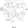
- FIG. 7B is a block diagram illustrating the quad multiplier of the PE in more detail
- FIG. 8 is a high-level block diagram illustrating a first example subcluster in more detail
- FIG. 9 is a high-level block diagram illustrating a second example subcluster in more detail.
- FIG. 10 is a high-level block diagram illustrating a first example cluster in more detail
- FIG. 11 is a high-level block diagram illustrating a second example cluster in more detail
- FIG. 12 is a high-level block diagram illustrating the inter-cluster crossconnect in more detail
- FIG. 13 is a diagram illustrating a first example memory windowing scheme
- FIG. 14 is a diagram illustrating a second example memory windowing scheme
- FIG. 15 is a diagram illustrating first example memory accessibility between compute and memory elements including window size and computer access configurability
- FIG. 16 is a diagram illustrating second example memory accessibility between compute and memory elements
- FIG. 17 is a diagram illustrating an example scatter/gather based resource windowing technique
- FIG. 18 is a block diagram illustrating an example memory contention resolution scheme
- FIG. 19 is a high-level block diagram illustrating a first example layer controller in more detail
- FIG. 20 is a high-level block diagram illustrating the layer controller interface to L3 memory and subclusters in more detail
- FIG. 21 is a high-level block diagram illustrating a second example layer controller in more detail
- FIG. 22 is a high-level block diagram illustrating an example NN processor compiler/SDK
- FIG. 23 is a diagram illustrating the flexible processing granularity of the NN processor and related memory versus latency trade-off
- FIG. 24 is a diagram illustrating a first example multi-NN processor SoC system of the present invention.
- FIG. 25 is a diagram illustrating a second example multi-NN processor SoC system of the present invention.
- FIG. 26 is a diagram illustrating a first example multi-NN processor SoC system of the present invention.
- FIG. 27 is a diagram illustrating a first example multi-NN processor SoC system of the present invention.
- FIG. 28 is a diagram illustrating an example mapping strategy for the first example artificial neural network of FIG. 2 ;
- FIG. 29 is a diagram illustrating a second example artificial neural network
- FIG. 30 is a diagram illustrating an example multi-NN processor SoC system of the ANN of FIG. 29 ;
- FIG. 31 is a diagram illustrating a third example artificial neural network
- FIG. 32 is a diagram illustrating a first example multi-NN processor SoC system of the ANN of FIG. 31 ;
- FIG. 33 is a diagram illustrating a second example multi-NN processor SoC system of the ANN of FIG. 31 .
- Any reference in the specification to a method should be applied mutatis mutandis to a system capable of executing the method. Any reference in the specification to a system should be applied mutatis mutandis to a method that may be executed by the system.
- the term “or” is an inclusive “or” operator, and is equivalent to the term “and/or,” unless the context clearly dictates otherwise.
- the term “based on” is not exclusive and allows for being based on additional factors not described, unless the context clearly dictates otherwise.
- the meaning of “a,” “an,” and “the” include plural references.
- the meaning of “in” includes “in” and “on.”
- the present invention may be embodied as a system, method, computer program product or any combination thereof. Accordingly, the present invention may take the form of an entirely hardware embodiment, an entirely software embodiment (including firmware, resident software, micro-code, etc.) or an embodiment combining software and hardware aspects that may all generally be referred to herein as a “circuit,” “module” or “system.” Furthermore, the present invention may take the form of a computer program product embodied in any tangible medium of expression having computer usable program code embodied in the medium.
- the invention may be described in the general context of computer-executable instructions, such as program modules, being executed by a computer.
- program modules include routines, programs, objects, components, data structures, etc. that perform particular tasks or implement particular abstract data types.
- the invention may also be practiced in distributed computing environments where tasks are performed by remote processing devices that are linked through a communications network.
- program modules may be located in both local and remote computer storage media including memory storage devices.
- the computer-usable or computer-readable medium may be, for example but not limited to, an electronic, magnetic, optical, electromagnetic, infrared, or semiconductor system, apparatus, device, or propagation medium.
- the computer-readable medium would include the following: an electrical connection having one or more wires, a portable computer diskette, a hard disk, a random access memory (RAM), a read-only memory (ROM), an erasable programmable read-only memory (EPROM or flash memory), an optical fiber, a portable compact disc read-only memory (CDROM), an optical storage device, a transmission media such as those supporting the Internet or an intranet, or a magnetic storage device.
- the computer-usable or computer-readable medium could even be paper or another suitable medium upon which the program is printed, as the program can be electronically captured, via, for instance, optical scanning of the paper or other medium, then compiled, interpreted, or otherwise processed in a suitable manner, if necessary, and then stored in a computer memory.
- a computer-usable or computer-readable medium may be any medium that can contain or store the program for use by or in connection with the instruction execution system, apparatus, or device.
- Computer program code for carrying out operations of the present invention may be written in any combination of one or more programming languages, including an object-oriented programming language such as Java, Smalltalk, C++, C# or the like, conventional procedural programming languages, such as the “C” programming language, and functional programming languages such as Prolog and Lisp, machine code, assembler or any other suitable programming languages.
- the program code may execute entirely on the user's computer, partly on the user's computer, as a stand-alone software package, partly on the user's computer and partly on a remote computer or entirely on the remote computer or server.
- the remote computer may be connected to the user's computer through any type of network using any type of network protocol, including for example a local area network (LAN) or a wide area network (WAN), or the connection may be made to an external computer (for example, through the Internet using an Internet Service Provider).
- LAN local area network
- WAN wide area network
- Internet Service Provider an Internet Service Provider
- These computer program instructions may also be stored in a computer-readable medium that can direct a computer or other programmable data processing apparatus to function in a particular manner, such that the instructions stored in the computer-readable medium produce an article of manufacture including instruction means which implement the function/act specified in the flowchart and/or block diagram block or blocks.
- the computer program instructions may also be loaded onto a computer or other programmable data processing apparatus to cause a series of operational steps to be performed on the computer or other programmable apparatus to produce a computer implemented process such that the instructions which execute on the computer or other programmable apparatus provide processes for implementing the functions/acts specified in the flowchart and/or block diagram block or blocks.
- the invention is operational with numerous general purpose or special purpose computing system environments or configurations.
- Examples of well-known computing systems, environments, and/or configurations that may be suitable for use with the invention include, but are not limited to, personal computers, server computers, cloud computing, hand-held or laptop devices, multiprocessor systems, microprocessor, microcontroller or microcomputer based systems, set top boxes, programmable consumer electronics, ASIC or FPGA core, DSP core, network PCs, minicomputers, mainframe computers, distributed computing environments that include any of the above systems or devices, and the like.
- the invention is operational in systems incorporating video and still cameras, sensors, etc. such as found in automated factories, autonomous vehicles, in mobile devices such as tablets and smartphones, smart meters installed in the power grid and control systems for robot networks.
- any computation device that can host an agent can be used to implement the present invention.
- FIG. 1 A block diagram illustrating an example computer processing system adapted to implement one or more portions of the present invention is shown in FIG. 1 .
- the exemplary computer processing system, generally referenced 10 for implementing the invention comprises a general-purpose computing device 11 .
- Computing device 11 comprises central processing unit (CPU) 12 , host/PIC/cache bridge 20 and main memory 24 .
- CPU central processing unit
- main memory 24 main memory
- the CPU 12 comprises one or more general purpose CPU cores 14 and optionally one or more special purpose cores 16 (e.g., DSP core, floating point, GPU, and neural network optimized core).
- the one or more general purpose cores execute general purpose opcodes while the special purpose cores execute functions specific to their purpose.
- the CPU 12 is coupled through the CPU local bus 18 to a host/PCI/cache bridge or chipset 20 .
- a second level (i.e. L2) cache memory (not shown) may be coupled to a cache controller in the chipset.
- the external cache may comprise an L1 or first level cache.
- the bridge or chipset 20 couples to main memory 24 via memory bus 20 .
- the main memory comprises dynamic random access memory (DRAM) or extended data out (EDO) memory, or other types of memory such as ROM, static RAM, flash, and non-volatile static random access memory (NVSRAM), bubble memory, etc.
- DRAM dynamic random access memory
- EEO extended data out
- the computing device 11 also comprises various system components coupled to the CPU via system bus 26 (e.g., PCI).
- the host/PCI/cache bridge or chipset 20 interfaces to the system bus 26 , such as peripheral component interconnect (PCI) bus.
- PCI peripheral component interconnect
- the system bus 26 may comprise any of several types of well-known bus structures using any of a variety of bus architectures. Example architectures include Industry Standard Architecture (ISA) bus, Micro Channel Architecture (MCA) bus, Enhanced ISA (EISA) bus, Video Electronics Standards Associate (VESA) local bus and Peripheral Component Interconnect (PCI) also known as Mezzanine bus.
- ISA Industry Standard Architecture
- MCA Micro Channel Architecture
- EISA Enhanced ISA
- VESA Video Electronics Standards Associate
- PCI Peripheral Component Interconnect
- Non-volatile memory e.g., disk based data storage
- video/graphics adapter 30 connected to display 32
- user input interface (I/F) controller 31 connected to one or more input devices such mouse 34 , tablet 35 , microphone 36 , keyboard 38 and modem 40
- network interface controller 42 peripheral interface controller 52 connected to one or more external peripherals such as printer 54 and speakers 56 .
- the network interface controller 42 is coupled to one or more devices, such as data storage 46 , remote computer 48 running one or more remote applications 50 , via a network 44 which may comprise the Internet cloud, a local area network (LAN), wide area network (WAN), storage area network (SAN), etc.
- a small computer systems interface (SCSI) adapter (not shown) may also be coupled to the system bus.
- the SCSI adapter can couple to various SCSI devices such as a CD-ROM drive, tape drive, etc.
- the non-volatile memory 28 may include various removable/non-removable, volatile/nonvolatile computer storage media, such as hard disk drives that reads from or writes to non-removable, nonvolatile magnetic media, a magnetic disk drive that reads from or writes to a removable, nonvolatile magnetic disk, an optical disk drive that reads from or writes to a removable, nonvolatile optical disk such as a CD ROM or other optical media.
- Other removable/non-removable, volatile/nonvolatile computer storage media that can be used in the exemplary operating environment include, but are not limited to, magnetic tape cassettes, flash memory cards, digital versatile disks, digital video tape, solid state RAM, solid state ROM, and the like.
- a user may enter commands and information into the computer through input devices connected to the user input interface 31 .
- input devices include a keyboard and pointing device, mouse, trackball or touch pad.
- Other input devices may include a microphone, joystick, game pad, satellite dish, scanner, etc.
- the computer 11 may operate in a networked environment via connections to one or more remote computers, such as a remote computer 48 .
- the remote computer may comprise a personal computer (PC), server, router, network PC, peer device or other common network node, and typically includes many or all of the elements described supra.
- PC personal computer
- server router
- network PC peer device
- Such networking environments are commonplace in offices, enterprise-wide computer networks, intranets and the Internet.
- the computer 11 When used in a LAN networking environment, the computer 11 is connected to the LAN 44 via network interface 42 . When used in a WAN networking environment, the computer 11 includes a modem 40 or other means for establishing communications over the WAN, such as the Internet.
- the modem 40 which may be internal or external, is connected to the system bus 26 via user input interface 31 , or other appropriate mechanism.
- the computing system environment is an example of a suitable computing environment and is not intended to suggest any limitation as to the scope of use or functionality of the invention. Neither should the computing environment be interpreted as having any dependency or requirement relating to any one or combination of components illustrated in the exemplary operating environment.
- the software adapted to implement the system and methods of the present invention can also reside in the cloud.
- Cloud computing provides computation, software, data access and storage services that do not require end-user knowledge of the physical location and configuration of the system that delivers the services.
- Cloud computing encompasses any subscription-based or pay-per-use service and typically involves provisioning of dynamically scalable and often virtualized resources.
- Cloud computing providers deliver applications via the internet, which can be accessed from a web browser, while the business software and data are stored on servers at a remote location.
- Computer readable media can be any available media that can be accessed by the computer and capable of storing for later reading by a computer a computer program implementing the method of this invention.
- Computer readable media includes both volatile and nonvolatile media, removable and non-removable media.
- Computer readable media may comprise computer storage media and communication media.
- Computer storage media includes volatile and nonvolatile, removable and non-removable media implemented in any method or technology for storage of information such as computer readable instructions, data structures, program modules or other data.
- Computer storage media includes, but is not limited to, RAM, ROM, EEPROM, flash memory or other memory technology, CD-ROM, digital versatile disks (DVD) or other optical disk storage, magnetic cassettes, magnetic tape, magnetic disk storage or other magnetic storage devices, or any other medium which can be used to store the desired information and which can be accessed by a computer.
- Communication media typically embodies computer readable instructions, data structures, program modules or other data such as a magnetic disk within a disk drive unit.
- the software adapted to implement the system and methods of the present invention may also reside, in whole or in part, in the static or dynamic main memories or in firmware within the processor of the computer system (i.e. within microcontroller, microprocessor or microcomputer internal memory).
- each block in the flowchart or block diagrams may represent a module, segment, or portion of code, which comprises one or more executable instructions for implementing the specified logical function(s).
- the functions noted in the block may occur out of the order noted in the figures. For example, two blocks shown in succession may, in fact, be executed substantially concurrently, or the blocks may sometimes be executed in the reverse order, depending upon the functionality involved.
- an ANN is essentially a function with a large number of parameters, mapping between an input space to an output space.
- an ANN can be viewed as a sequence of computations.
- ANNs have a certain internal structure and a set of properties.
- the neural network (NN) processor comprises a plurality of basic computation units doing the same or similar mathematical manipulations, which, when combined together make up the neural network.
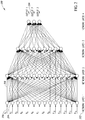
- the example ANN generally referenced 350 , comprises four network layers 352 , including network layers 1 through 4 .
- Each network layer comprises a plurality of neurons 354 .
- Inputs X 1 to X 14 are input to network layer 1 .
- Weights 358 are applied to the inputs of each neuron in a network layer. The outputs of one network layer forming the input to the next network layer until the final outputs 359 , outputs 1 through 3 , are generated.
- the architecture of the present invention comprises a multi-layer architecture (i.e. not referred to ANN layers) that addresses the computational needs of an artificial neural network to its full capacity.
- multi-layer refers to an approach similar to that of the well-known ISO OSI-layer model for networking which describes the overall solution at varying levels of abstraction.
- the equivalent model for neural network processing comprises six layers, including: Layer 1 (Physical 412 ) comprising the physical primitives making up the various units; Layer 2 (Unit 414 ) comprising the basic computational unit that underlies the neural network; Layer 3 (Interconnect 416 ) comprising the interconnect fabric that provides the network connectivity; Layer 4 (Management 418 ) providing network level flow control, monitoring and diagnostics; Layer 5 (Interface 420 ) providing the application layer interface and mapping to architecture primitives; and Layer 6 (Application 422 ) comprising the neural network based application.
- Layer 1 Physical 412
- Layer 2 Unit 414
- Layer 3 Interconnect 416
- Layer 4 Management 418
- Layer 5 Interface 420
- Layer 6 Application 422
- FIG. 4 A high-level block diagram illustrating an example system on chip (SoC) NN processing system comprising one or more NN processing cores is shown in FIG. 4 .
- the SoC NN processing system generally referenced 100 , comprises at least one NN processor integrated circuit (or core) 102 optionally coupled to one or more additional internal or external NN processors 104 via one or more suitable chip to chip interfaces, a bus fabric 106 adapted to couple the NN processor to various system on chip elements 108 , microcontroller unit (MCU) subsystem 118 , and one or more interfaces 126 .
- MCU microcontroller unit
- the SoC 108 includes bootstrap circuit block 110 , debug circuit block 112 , power circuit block 114 , and clock circuit block 116 .
- the MCU subsystem 118 includes a controller circuit block 120 , instruction memory 122 , and data memory 124 .
- Interfaces 126 comprise a pin multiplexer 139 , and one or more well-known interfaces including camera serial interface (CSI) 128 , display serial interface (DSI), Ethernet 132 , universal serial bus (USB) 134 , inter-integrated circuit (I 2 C) interface 136 , serial peripheral interface (SPI) 137 , and controller area network (CAN) interface 138 . Note that these interfaces are shown as an example, as any combination of different interfaces may be implemented.
- CSI camera serial interface
- DSI display serial interface
- USB universal serial bus
- I 2 C inter-integrated circuit
- SPI serial peripheral interface
- CAN controller area network
- FIG. 5 A high-level block diagram illustrating an example NN processing core in more detail is shown in FIG. 5 .
- the NN processing engine or core 60 comprises several hierarchical computation units.
- the lowest hierarchical level is the processing element (PE) 76 with its own dedicated internal Layer 1 or L1 memory 78 in which individual neurons are implemented.
- a plurality of N PEs 76 along with dedicated Layer 2 or L2 memory 74 make up the next hierarchical level termed a subcluster 70 .
- a plurality of M subclusters 70 along with dedicated Layer 3 or L3 memory 72 , a plurality of activation function circuits 80 , and a plurality of layer controller (LC) circuits 82 make up a cluster 66 .
- PE processing element
- L1 memory 78 A plurality of N PEs 76 along with dedicated Layer 2 or L2 memory 74 make up the next hierarchical level termed a subcluster 70 .
- a plurality of L clusters along with dedicated Layer 4 or L4 memory 64 are in the NN processor core 60 which also comprises NN manager circuit 62 , and memory interface 68 to off-chip Layer 5 or L5 memory 98 .
- a plurality of bus interfaces 86 (i.e. chip-to-chip interfaces) couple the NN processor to other off-chip NN processor chips for additional network capacity.
- Bus interface 84 (i.e. chip-to-chip interface) couples the NN processor to a conventional rule based machine (RBM) co-processor 88 comprising a CPU 90 , instruction memory 92 and data memory 94 .
- the RBM co-processor is optionally coupled to the NN device 60 via a suitable interface, e.g., GPUs, I 2 C, etc.
- the NN processor can be implemented having any desired number of hierarchical levels as well as any number of computation units within each level and is not limited to the examples described herein which are provided for illustration purposes only.
- any number of activation functions 80 and layer controllers 82 may be implemented in the cluster level or in any other level depending on the design goals and particular implementation of the NN processor.
- the NN manager 62 is a specialized processor that controls two data pipes: one parallel and one serial along with functions to drive the network fabric.
- This processor carries out special purpose operations that are native to the control plane of the neural network.
- Example operations includes, but are not limited to, Infer, Train, Load weights, and Update weights.
- Load balancing and resource allocation are handled by an external software tool chain, which includes a set of tools including a compiler, mapper, and allocator, that address these tasks.
- the NN processor includes shared memory for the storage of weights and dedicated memory elements are for storing contexts thereby enabling relatively high data processing bandwidth.
- the NN processor includes data and control planes that are strictly separate from each other and that provide out of band control to the computation elements.
- the NN processor includes a configurable interconnect between aggregation levels to yield a dynamic and programmable data pipeline.
- the NN processor is capable of implementing multiple ANNs in parallel, where each ANN has one or more network layers.
- the NN processor is adapted to simultaneously process one or more input data streams associated with the ANNs. Since the architecture of the NN device resembles the structure of an ANN, multiple ANNs can be viewed as a single wide ANN. Note that when deploying multiple ANNs, given enough resources, the mapper in the external tool chain is operative to map available resources while the NN manager governs event triggers. In this case, due to the enormous parallelism of the device, each set of resources grouped within a ‘layer’ of the ANN is independent from each other.
- computation elements of the NN processor are operative to function at any desired granularity of a subset of the input data stream thereby trading off memory element usage versus latency, as described in more detail infra.
- the NN processor of the present invention uses several design principles in its implementation including: (1) just in time usage of system resources; (2) dynamic allocation of system resources per need; (3) leveraging both the time-domain and the space-domain to optimize utilization and efficiency; and (4) balanced load over available system resources.
- ANNs are implemented in three stages: modeling, training, and inference, all three of which are addressed to some extent by the NN processor of the present invention.
- the NN processor is capable of altering the model representation statically and dynamically thus reflecting its flexible nature.
- the ‘processor’ notation is used as opposed to an ‘accelerator’ since the latter is typically adapted a priori to exercise a predefined set of operations.
- the NN processor supports on-the-fly and complementary training operations that allows implementation of the training procedure. This includes: (1) running back and forth through the network (i.e. backpropagation); (2) dynamically applying dropout; and (3) on-the-fly evaluation of layer performance and ill behavior detection.
- the ANN is executed optimally and efficiently and is applied to new inputs.
- the NN processor of the present invention combines several features that combine together to provide extremely high computation rate, small chip footprint, low power consumption, scalability, programmability, and flexibility to handle many types of neural networks.
- a first feature comprises the compute fabric (or compute capability) provided by the computation units that are organized into various aggregation levels or hierarchical levels, such as PEs, subclusters, clusters, NN cores as described in the example system disclosed herein.
- the compute fabric comprises the basic compute elements that are configured to address the special nature of the computational needs of ANNs.
- Several features of the compute fabric include: (1) a lean circuit architecture thereby allowing a relatively large number of physical entities to be implemented; (2) a large number of multiply and accumulate operations at once, where additions are performed as accumulations; (3) flexibility of number representation, including integer and floating point as well as different bit widths; (4) quad-multiplier support allowing for higher resolution computations; and (5) N-way ALU support to provide the capability of optimizing memory bandwidth, i.e. instead of performing a single operation per cycle such as y ⁇ y+w*x, a more complex operation such as y ⁇ y+w 1 *x 1 +w 2 *x 2 can be implemented which reflects a trade-off between an increase in silicon complexity and reduced memory access required.
- a second feature is the control plane and the strict separation of the control fabric from the data fabric which enables aggregation of control as well as very ‘lean’ or ‘slim’ control of the entire data fabric (i.e. data plane).
- the control plane is separate from the data plane and thus it can be aggregated in the sense that a large number of compute units are controlled using relatively few control lines, e.g., by a single control line in some cases. For example, considering the multiply circuits in the PEs, a single control signal initiates the multiply operation in thousands of PEs at the same time.
- the programmability of the control plane is separate from the programmability of the data plane.
- the massive parallelism of the data fabric of the NN core is matched by the lean structure of the control plane.
- out-of-band control is in contrast to traditional microcontroller based techniques as it is not a Von-Neuman machine based technique.
- control remains programmable.
- the non-rigid implementation of the control fabric and the general nature of the computation units allows the NN core to handle numerous types of ANNs, such as convolutional NNs (CNNs), recurrent NNs (RNNs), deep NNs (DNNs), MLPs, etc., as well as more intricate implementations of the above and subtle combinations and properties of each, e.g., stride, padding, etc. implemented in convolutional modes.
- CNNs convolutional NNs
- RNNs recurrent NNs
- DNNs deep NNs
- MLPs etc.
- a third feature is the structure of the memory fabric including memory windowing.
- high bandwidth access to the memory is provided in parallel to a large number of computation units. This is achieved by narrowing access for a particular computation unit to only a small portion of the memory. Thus, full random access to the entire memory is not provided. Rather, access to only a relatively small window of memory is provided. This allows simultaneous access across thousands of computation units, thus representing a tradeoff between bandwidth and random accessibility. Since a single compute unit memory access pattern is structured and well-defined by the ANN and does not require full random access to the entire memory, access can be ‘windowed’ to only those few memory blocks required for that particular compute unit. Thus, extremely high memory bandwidth is achieved whereby thousands of compute units can access memory simultaneously in parallel with the tradeoff being access only to memory that is ‘local’ to the compute unit.
- the architecture of the NN processor comprises a control plane and a data plane (or control fabric and data fabric).
- the control plane is responsible for configuring and controlling all the data computation units in the NN processor. It comprises a dataflow machine or processor incorporating, in one embodiment, microcode tailored for neural network operations.
- the control plane governs the cluster entities 66 which functions as an aggregator for the next layer of aggregation, i.e. the subcluster 70 .
- the subcluster comprises the most basic units, namely the processing elements (PEs) 76 which are composed of a multiply and accumulate (MAC) circuit and local memory. It is the PE hierarchical level that contains a set of neuron entities found in a typical neural network.
- an important aspect of implementing an ANN in the NN processor is the control and interconnect of all the compute elements.
- the very large number of compute elements in an ANN is leveraged by the present invention.
- One feature of the device control fabric is that it is relatively very lean since it is shared among a large set of compute resources.
- the NN processor features (1) strict separation between data and control, where the control signaling is performed out of band and does not include any data driven memory access; (2) dynamic mapping between control and attached compute resources; and (3) flexibility and programmability of the control fabric (i.e. at compile time).
- the NN processor includes layer controllers incorporating microcode machines that allow full accessibility to the control signaling of the computational elements, memory etc.
- data driven memory access denotes access that involves observation of the data that flows through the data pipeline.
- the NN processor does not require this.
- data driven memory access is common in rule based machines since the nature of the rules is data dependent and thus control must be intertwined with data. For example, consider the statement: if (x>some_value) then do A. This implies the need to observe every input ‘x’. In contrast, consider a machine that compares many inputs with a threshold. The microcode in this case only needs to trigger an operation that applies a massive set of comparators. Such an approach, however, cannot be taken in an RBM because it implies a huge number of operations that must be hardwired which negates the possibility of programing the machine.
- the NN processor in contrast, operates on data using a very limited set of operations.
- the nature of the processing flow does not involve the value of the data.
- a control bus of 64 control signals is needed to control thousands of compute units.
- the NN processor is implemented such that functionality is provided at several points of aggregation where it is needed, as described in more detail infra.
- the NN processor is configured to be substantially balanced in terms of compute and memory resources to ensure the system achieves maximal utilization.
- bus interfaces 86 provide for interconnecting additional NN processors 96 to extend beyond the limitations of a single processor.
- an RBM coprocessor subsystem 88 is configured to support one or more primitives that are not supported by the NN processor.
- the coprocessor functions to exchange tasks extracted from the ANN and assigned to the RBM.
- the NN processor essentially operates as a dataflow machine meaning that the calculations are executed based solely upon the availability of data.
- the data flow is divided between layers, which are analogous to the layers in the ANN.
- the computation units inside a layer act synchronously, starting when data is ready at the layer's input and ending when they need new data and/or need to pass results to the next layer, at which point the layer's state machine synchronizes with the previous and/or next layer's state machine.
- an MLP network with two dense layers can be mapped as (1) one layer which receives input from outside the core, (2) two layers which represent the neural network layers, and (3) one layer which sends the result outside the core.
- the input layer waits until it receives all the inputs (e.g., 784 inputs for the well-known MNIST data set), and then signals layer 1 that its input is ready. Layer 1 then performs all the required multiply and accumulate (MAC) operations, the activation function, and finally signals to layer 2 , which in turn repeats the same steps. When layer 2 is finished, it signals to the output layer to send the results outside the NN core.
- all the inputs e.g., 784 inputs for the well-known MNIST data set
- the NN core starts the MACs in layer 1 on a smaller portion of input data, thus reducing the buffering required between the input layer and layer 1 , at the expense of complexity of the state machine in layer 1 and possibly loss of compute efficiency during signaling.
- data is passed through shared L3 memory 72 , while the signaling is performed through a dedicated interconnect 282 ( FIG. 11 ), described in more detail infra.
- a dedicated interconnect 282 FIG. 11
- the AXI4-Stream protocol is used between clusters, which handles both data and control planes.
- the interconnect between the layers provides a dual buffer mechanism, so that one layer writes its output to one buffer as the second layer reads the previous output as its input from the second buffer.
- the use of the dataflow architecture together with a relatively limited set of basic operations in neural networks enables a significant reduction in the requirements of control distribution.
- each dynamic ‘instruction’ actually comprises multiple instructions instructing all the compute elements in a layer what to do in each cycle.
- the basic instructions themselves are relatively simple. Repetitions (i.e. loops) and jump instructions are provided out of band, to avoid wasting cycles.
- microcode since the microcode is very compact, it can reside in on-chip SRAM without the need for prefetch, branch prediction, etc.
- a layer comprises many processing elements (PEs)
- PEs processing elements
- only one central state machine is needed to control the steps of the computation for the entire layer along with smaller slave state machines which store only a sub-state, with each of them controlling multiple PEs.
- a global enable bit starts execution of all the state machines, and a global synchronous reset signal returns them to an initial state. Note that reset has no effect on the configuration memory and the data memory as the control plane ensures that no invalid data is used.
- model is used to describe a quasi-static configuration which defines the dynamic behavior of all the compete units in the NN core.
- a model is typically analogous to a ANN model, but there may be other types of models, such as a model loaded for debug purposes or for loading weights into memory.
- the configuration space is exposed in a memory-like interface, where modules are addressed using a hierarchical address space.
- Weights loading is normally performed before the configuration of the model and is achieved by configuring control signaling which copies the weights into the relevant memory blocks and sets the enable bit.
- the inference model is then loaded while the cluster is disabled, the control is reset and finally the cluster is enabled.
- the memory fabric of the NN processor is designed to address the inherent nature of ANNs.
- the memory is structured in a hierarchical manner in order to address the needs of the various memory consumers. These consumers include: (1) inter-layer data (i.e. cross layer input/output); (2) intra-layer information (i.e. contexts or intermediate results); and (3) weights.
- the various memory layers e.g., five in the example embodiment disclosed herein, go from smaller, efficient, more localized memory to larger, less efficient, global memory.
- the memory fabric is organized and constructed utilizing the following: (1) localization of memory where computing elements require access to local data which permits accessibility of any given computing element to a predefined and limited memory entity; (2) structured organization whereby memory content is organized a priori in a given consistent matter; (3) limited recall nature (i.e. read once) where most of the data is volatile by nature and once processed, is fully consumed with limited or no need for further access to it; and (4) pipelined operation where the output data of one compute element serves as the input data to another compute element.
- each hierarchical level contains its own local memory.
- PEs comprise L1 memory
- subclusters comprise L2 memory
- clusters comprise L3 memory
- NN cores comprise L4 memory
- L5 memory is located externally off-SoC.
- An example memory hierarchy is presented below in Table 1.
- N represents the number of processing elements in a subcluster
- M is the number of subclusters in a cluster
- L is the number of clusters in the NN processor device. Note that the size indicated for each memory level L1 through L5 are for illustration purposes only. It is appreciated that any desired memory size for the various memory layers may be implemented without departing from the scope of the invention.
- the lower memory layers e.g., L1 in the PE
- the upper memory layers e.g., L4 in the NN core, are much larger sized by carry far less traffic.
- this ‘spillover’ is a quasi-static feature, as the resource requirements are already known once the model is selected, and thus does not require complex arbitration. This feature allows the static allocation of a significantly lower amount of memory resources in each layer since they are allocated according to the nominal case rather than the worst case.
- ‘gradual’ allocation of memory also features a sliding window mechanism, described briefly supra, which is used in L3 memory and described in more detail infra.
- PE Processing Element
- the basic compute unit is the processing element (PE).
- PE processing element
- a block diagram illustrating an example low-level processing element (PE) in more detail is shown in FIG. 6 .
- the PE generally referenced 140 , comprises one or more multipliers 142 controlled by multiply trigger 177 , an adder 144 controlled by adder trigger 171 , L1 memory 150 comprising a plurality of registers 152 , destination multiplexer 146 controlled by destination control 175 , source multiplexer 148 controlled by source control 173 , write multiplexer 154 controlled by output shuffle control 178 , and read multiplexer 156 controlled by input shuffle control 179 .
- Input (x) data 161 from input memory 158 and weights (w) 163 from weight memory 160 are provided to the multiplier(s) 142 in accordance with an input control and weight control, respectively.
- the basic compute unit is a PE and comprises a multiply/accumulate entity that reflects the intrinsic operation of a neuron.
- the intermediate result or outcome is stored in L1 memory 150 which is local to the PE.
- the depth P of L1 memory reflects the number of simultaneous ‘neurons’ or ‘contexts’ a PE can handle. Note that more than P neurons (i.e. contexts) can be handled by storing intermediate results for additional neurons in L2/L3 memory. Latency is impacted in that additional time is required to process the additional neurons.
- Providing P neurons leverages both the spatial domain by limiting the computational construct to the bare minimum, while also leveraging the time domain by storing multiple contexts.
- the capability of handling internal context provides for a number of capabilities such as: (1) the ability to assign multiple logical neurons to a single physical neuron (each context stores the output of one neuron); (2) storing multiple intermediate results for the same input resulting in simultaneous operations, and hypothesis testing for different versions of weights (e.g., backpropagation results, correction values based on gradients, etc.); (3) multithreaded inference of the same inputs for the purpose of applying common methodology of a network committee and a majority vote extraction; (4) running multiple networks if resources are available; and (5) load balancing based on overall network capacity as governed by an NN manager.
- capabilities such as: (1) the ability to assign multiple logical neurons to a single physical neuron (each context stores the output of one neuron); (2) storing multiple intermediate results for the same input resulting in simultaneous operations, and hypothesis testing for different versions of weights (e.g., backpropagation results, correction values based on gradients, etc.); (3) multithreaded inference of the same inputs for the purpose of
- Equation 2 above reflecting neuron functionality is spread over multiple time instances and implemented as provided below in Listing 1. Note that this is an example implementation only as other sequences may be used by loading different microcode to the layer controllers (LCs) 642 ( FIG. 20 ).
- LCs layer controllers
- P ⁇ 1 Apply calculation according to configured representation, based on subcluster ctrl. Target is stored in place unless otherwise indicated by control signals.
- the PE comprises separately controlled counting elements for the weights (w) and inputs (x) as well as separate control over the representation format for the adder and multiplier. It also comprises separately controlled ingress/egress L1 entry index, allowing the order of calculations to be manipulated.
- the intermediate results of the accumulation function are stored locally in the L1 memory registers 152 .
- pre-processing during initialization enables L1 memory to be pre-loaded with default values (e.g. prior intermediate results, bias values, etc.).
- the PE also includes intermediate memory aggregation control, i.e. allocation step size.
- activation functions are aggregated to minimize area overhead and not implemented at the PE or subcluster level but rather at the cluster level.
- the PE also supports activation bypass to permit concatenation.
- the output 151 of the adder 144 can be steered via destination mux 146 using destination control 175 to either (1) the activation function via path 162 ; (2) to L2 or L3 memory via path 164 ; or (3) to the source mux 148 via path 166 .
- the source mux 148 selects via source control 173 either (1) the output from the adder; or (2) an intermediate result from L2 or L3 memory 168 .
- the write mux selects via output shuffle select 178 one of the neuron registers 152 to write the output of the source mux to via one of P paths 172 .
- the data written to the L1 memory typically comprises intermediate results generated as a result of the multiply and accumulate operations performed over many cycles.
- Data is read out of the L1 memory via one of P paths 174 connecting the neuron registers to the read mux 156 and selected via input shuffle control select 179 .
- the output 176 of the read mux forms one of the two inputs to the adder 144 .
- the other input to the adder being the output of the multiplier 142 .
- a pre-adder (not shown) functions to add the outputs of the multipliers to generate a single sum that is then input to the adder 144 .
- FIG. 7A A block diagram illustrating a second example low-level processing element (PE) in more detail is shown in FIG. 7A .
- the PE is the most basic compute element of the NN processor.
- the neurons of the ANN are implemented in the PE, essentially in the L1 memory.
- the processing element generally referenced 450 , comprises an input data representation circuit 452 , multiplier circuit 454 , representation transformation/rounding circuit 456 , accumulator (i.e. adder) 458 , L1 memory 460 , negate circuit 472 , and multiplexer 474 .
- input data (X) 468 and weights (W) 470 are input from L3 memory to the input data representation circuit 452 .
- This circuit is operative to transform the representation of the input data and/or weights from integer to floating point (FP) format and vice versa in accordance with an INT/FP signal 462 which is also input to the multiplier.
- the resulting X 504 and W 506 are input to the multiplier 454 . Note that either of the two PE embodiments shown in FIGS. 6 and 7A may be used in the NN device of the present invention.
- the multiplier comprises several multipliers that operate in parallel.
- the multiplier is capable of multiplying both integer and floating point numbers.
- the number of significant bits for the input data and weights can also vary as set by the control inputs 464 , 466 , respectively.
- the product output of the multiplier 486 is input to the representation transformation/rounding circuit 456 .
- FP accumulator and FP input control inputs 508 , 510 respectively, signal circuit 456 whether the product is integer or FP format.
- the circuit 456 functions to perform rounding of the product before input to the accumulator.
- the output 488 of circuit 456 is input to the accumulator (adder) 458 .
- the second input to the accumulator 496 comprises either a context (i.e. intermediate result) 490 from L2 or L3 memory or the output of local L1 memory 460 .
- Multiplexer 474 selects between the two in accordance with SEL 476 .
- the output 494 is input to a negate circuit 472 where, in accordance with a Negate control 478 , the output 496 is negated before being input to the accumulator.
- Additional configuration controls to the accumulator include an accumulator shift signal (accumulator_shift) 498 , accumulator enable (accum_en) 500 , and FP accumulator 502 .
- the output 484 of the accumulator is written to the L1 memory.
- the L1 memory also includes L1 output select 480 and zero skip 482 .
- Intermediate results (i.e. contexts) output from the L1 memory are either input to the accumulator via path 493 or written to L2 or L3 memory via path 492 .
- accumulated (i.e. intermediate) results are written to and read from L1 memory sequentially, i.e. there is no random access to the neuron registers in L1 memory.
- L1 memory may be accessed using any suitable predefined pattern other than randomly, e.g., sequential (one by one), skip one, skip two, etc. This greatly simplifies the addressing required to access the neuron registers.
- access to and from L2 and L3 memory layers is provided in the event not enough local L1 memory is available for a particular ANN. In this case, intermediate results are stored in higher memory layers to accommodate the particular ANN. The tradeoff, however, is increased latency in accessing the higher memory layers.
- a higher precision multiplication (e.g., 16-bit) is performed by combining four low precision (e.g., 8-bit) multipliers to generate a high (or double) precision (e.g., 16-bit) product.
- a block diagram illustrating the quad multiplier of the PE in more detail is shown in FIG. 7B .
- the quad multiplier, generally referenced 870 comprises four lower precision (e.g., 8-bit) multipliers 872 , Q 0 , Q 1 , Q 2 , and Q 3 .
- the input to the quad multiplier is a double precision input X made up of two low precision (e.g., 8-bit) values, namely X L 873 and X H 871 , and a double precision weight W also comprising two low precision (e.g., 8-bit) values, namely W L 880 and X H 882 .
- each basic unit Q i receives a low precision (e.g., 8-bit) W and X value and based thereon, the quad multiplier circuit generates the result Y ⁇ Y+W*X.
- a low precision e.g. 8-bit
- each output Y L and Y H represents a 16-bit number to yield a 32-bit multiplication product Y. It is appreciated that results of greater precision can be obtained using additional multipliers and suitable combination of input, weight and carry components.
- FIG. 8 A high-level block diagram illustrating a first example subcluster in more detail is shown in FIG. 8 .
- the subcluster, generally referenced 180 comprises a plurality of N PEs 182 , each individual PE 182 including local L1 memory 184 , interconnect fabric 186 , dedicated local L2 memory 188 portioned into a plurality of allocated memory blocks 190 , configuration and decode block 192 , and control/data signals 181 .
- the configuration/decode circuit 192 receives instructions from an external control bus 194 .
- Each subcluster 180 also communicates with input/output alignment circuit 196 and activation circuit 198 which in the example embodiment presented herein are located in the cluster hierarchy level, as described in more detail infra.
- the subcluster encapsulates the next level of memory hierarchy, i.e. the L2 memory layer that stores interlayer and intermediate results.
- it also includes the activation function circuits (i.e. represented by ⁇ in Equation 2 supra).
- the example NN core moves the activation function to the cluster level.
- the activation function regardless of its location receives the outputs of the neurons and is triggered once per N multiply and accumulate operations. Note that the number and location of the activation function circuits are selected to reflect optimal utilization of hardware.
- subcluster Several features of the subcluster include: (1) a distributed control scheme to manage memory access; (2) dynamic allocation of L2 memory for weights and intermediate results; (3) inherent intermediate results shuffling support to seamlessly augment L1 memory; (4) layer-centric information and diagnostics storage; (5) layer-centric pre-processing; (6) layer-centric post-processing; and (7) in-layer split support (e.g., for quantization segmentation).
- FIG. 9 A high-level block diagram illustrating a second example subcluster in more detail is shown in FIG. 9 . While FIG. 8 reflects a mostly logical view of the subcluster, FIG. 8 reflects a more physical view.
- the subcluster generally referenced 200 , comprises dedicated local L2 memory 210 , a plurality of N PEs 212 , each with its own L1 memory 214 and receiving enable EN 211 , PE control signal 213 , and PE configuration signal 215 , input interconnect 206 , output interconnect 208 , subcluster configuration 202 which receives instructions from the subcluster control bus 230 and outputs L2_cbus 236 , and subcluster decoder 204 which receives layer control 232 and group control 234 and outputs address ADDR 238 , enable EN 240 , and select SEL 242 .
- input data 216 and weights 218 are provided from the L3 memory at the cluster level to the input interconnect 206 in accordance with control signal 201 .
- the input interconnect feed input data 244 and weights 246 to the PEs 212 .
- a zero_skip signal 217 notifies the PEs that either the input data or weights have zero values and thus a multiply and add operation are not needed.
- weights 220 may also come from local L2 memory 210 , which receive address ADDR 205 , enable EN 207 , and control L2_cbus 209 .
- intermediate results 248 are read out and output to the output interconnect 208 via control signal 203 .
- Intermediate results can then be written to local L2 memory via path 226 or written to L3 memory via path 221 , multiplexer 222 , and path 228 .
- intermediate results 224 can be read from L2 memory and either transferred to L3 memory via multiplexer 222 or to the output interconnect which then forwards it to the PEs via path 249 .
- each subcluster comprises flexible and programmable pathways for feeding input data and weights to the neurons in the PEs as well as steering intermediate results from the neurons to and from either L2 or L3 memory.
- a subcluster is dedicated to the execution of a single ANN layer or a portion of it. Its function is to receive external inputs from L3 memory, perform multiply and adds with weights from either local L2 or external L3 memory, store intermediate results (also referred to as ‘contexts’) in PE L1 memory (or in local L2 memory when L1 memory is not sufficient), and finally send the results to the external activation function for normalization and activation.
- the subcluster decoder 204 functions to combine static input from the subcluster configuration 202 with dynamic input, both the common layer control and the timing group control.
- the state it stored includes counters which hold the following addressing: (1) weights read/write address; (2) contexts read address; (3) contexts write address; (4) activation source address (which PEs output for reading).
- the input interconnect is operative to (1) selects between external weights (i.e. L3 memory) or local weights (i.e. from L2 memory); (2) select the width of the weights memory, i.e. the number of weights selected and the depth of the memory where the maximum width allows all PEs to receive a different weight from L2 memory, or from L3 external memory; (3) select the weights to pass to the PEs from the selected weights source (using the MSBs of the address); select the width of the input bus; and (4) select the inputs to pass to the PEs from the selected input source (using the MSBs of the address).
- external weights i.e. L3 memory
- local weights i.e. from L2 memory
- select the width of the weights memory i.e. the number of weights selected and the depth of the memory where the maximum width allows all PEs to receive a different weight from L2 memory, or from L3 external memory
- select the weights to pass to the PEs from the selected weights source using the MS
- L2 memory 210 is used to store both weights and contexts in the same block.
- the weights addresses start from zero and count upwards while the contexts addresses start from the end of the memory. It is the responsibility of the control plane to prevent overflows.
- the cluster comprises a plurality of M subclusters, each subcluster 266 having its own L2 memory 268 , dedicated local L3 memory 262 portioned into a plurality of allocated memory blocks 264 , memory management unit (MMU) 260 adapted to interface L3 memory to the subclusters, management and control block 252 including control synchronizer 254 and a plurality of layers control circuits 256 , a plurality of input aligners 274 , and a plurality of activation function circuits 276 .
- I/O Input/output
- the cluster is the next level of aggregation typically representing more than one neural network layer. It contains both the subclusters which contain the PE basic computational entities as well as the interconnect fabric amongst subclusters. This provides the NN core with the flexibility to represent different neural network models by controlling the connectivity between subclusters.
- the L3 memory 262 functions to store interlayer results in one or more allocated memory blocks 264 .
- a distributed control scheme to manage memory access
- flexible configurable routing matrix to support representation of the total M subclusters into multiple layers
- interlayer control to allow data flow throttling and load balancing.
- Additional features include: (1) weight/input data balancing; (2) pre and post-processing blocks; (3) dynamic bus width and memory bit cell; (4) input data and weights interchangeability in the MMU; (5) the capability to provide event-driven behavior and pipelining; (6) control is decoupled from the data plane; (7) optional zero pipeline capability; and (8) balanced capability of runtime configuration modification.
- the cluster generally referenced 280 , comprises a cluster interconnect circuit 282 , input buffers 284 , output buffers 292 , plurality of M subclusters 306 , subcluster interconnect 304 , a plurality of activation function/pooling circuits 300 , a plurality of input aligner circuits 302 , and L3 memory 296 including a plurality of allocated memory blocks 298 .
- Input data and weights 286 are stored in the input buffers 284 . From the input buffers the input data and weights 288 are input to the cluster interconnect 282 . Input data 305 and weights 307 can also be written to and read from L3 memory 296 . Input data 281 from the cluster interconnect is input to the aligner circuit 302 before being input to the subcluster interconnect 304 . Input data 285 is fed to the subclusters 306 from the subcluster interconnect while output 283 from the subclusters is sent to the subcluster interconnect. The output 309 is input to the activation functions/pooling circuits 300 where the resulting output 308 is input to the cluster interconnect 282 . Output data 290 is written to the output buffers 292 . Data output 294 is then sent to other clusters or off-chip.
- the NN core supports multiple neural networks in parallel.
- Each cluster is operative to expose a control interface (e.g., clock, reset, enable, etc.), a configuration interface (memory like) and data interfaces (e.g., Advanced Extensible Interface (AXI)).
- AXI Advanced Extensible Interface
- Each cluster is adapted to implement one or more ANN layers, possibly from more than one ANN.
- the AXI interconnect exposes a control interface, and is used to connect the clusters, the DMA engine of an ARM controller in the NN core, and external ports.
- the ARM exposes an AXI interface through a DMA engine, control and configuration interfaces to the clusters and the interconnect, and external standard interfaces.
- clusters comprise: (1) configuration circuit; (2) memory management unit (MMU); (3) control interconnect; (4) trigger interconnect; (5) multiple subclusters; (6) multiple layer controllers (LCs); (7) multiple special purpose units; (8) multiple input units; (9) multiple output units; and (10) multiple memory blocks (i.e. L3 memory).
- MMU memory management unit
- LCs layer controllers
- special purpose units i.e. L3 memory
- the cluster supports multiple ANN layers in parallel, possibly from multiple ANNs.
- a network layer can be implemented as a layer controller (LC) with one or more subclusters connected through the control interconnect, or one of the special units (special purpose, input or output) which contains the control within.
- Layers communicate data through the allocated memory blocks 298 in L3 memory 296 , using signaling for flow control over the trigger interconnect, all defined by the configuration.
- the allocated memory blocks are also used as weight memory for the subclusters. All the control signals from the various layers to the L3 memory are translated by the MMU 260 from virtual to physical addresses using the configuration.
- the MMU uses a sliding overlapping window mechanism between two communicating port groups, such as the read ports of the L3 memory and the input ports to the subcluster.
- Each subcluster can choose its input from a group of memory ports around its relative place in the list of subclusters.
- the window mechanism is described more detail infra.
- the allocation of subclusters for each ANN layer is preferably proportional to the number of computations required in the ANN layer per feed.
- the allocation is determined by the control interconnect, which maps the subclusters to the LCs.
- the mapping is performed in two levels: (1) each subcluster is assigned to an LC through a sliding overlapping window mechanism (i.e. similar to that used in the MMU); and (2) the subcluster is assigned to a timing group inside the ANN layer.
- the timing groups spreads over time the actions requiring common resources, such as the write port to L3 used after activation.
- An ANN layer may comprise one or more timing groups, each containing one or more subclusters.
- the controls, which are common among all timing groups, are not passed through the second selection level, reducing multiplexing complexity of the circuit.
- the signaling mechanism between ANN layers is based on two bi-directional wires, which negotiate on the state of the dual buffer between them. Therefore, two bidirectional lines are required to connect two consecutive layers, i.e. each layer uses four bidirectional lines, two for the previous layer and two for the next layer.
- the two backward signals indicate whether the buffer ready for receiving new data for each one of the two buffers between the layers, and the two forward signals indicate whether the data in the buffer is valid for both buffers.
- the controller can flip the meaning of the two buffers (i.e. active and passive) in both directions, using a dedicated instruction.
- FIG. 12 A high-level block diagram illustrating the inter-cluster crossconnect in more detail is shown in FIG. 12 .
- the inter-cluster interconnect fabric/crossconnect generally referenced 430 , comprises a plurality of multiplexers 432 and splitters 440 that enable communications between clusters 436 .
- each cluster J comprises a plurality of ports, including input ports 396 and output ports 398 . Four input and output ports are shown in the example but any number can be implemented.
- Multiplexers 432 on the input side are controlled by SEL lines 438 .
- the inputs 434 to each multiplexer comprise output lines from neighboring clusters, e.g., clusters J ⁇ 2, J ⁇ 1, J, J+1.
- the output 444 from each multiplexer is input to a separate input port 396 in a cluster.
- splitters 440 on the output side generate outputs 442 that are fed to input lines of neighboring clusters, e.g., clusters J ⁇ 1, J, J+1, J+2.
- the output 446 from each output port 398 of a cluster is input to a separate multiplexer 440 .
- the NN manager 392 functions to control the configuration of the crossconnect 430 .
- connections to cluster J via inputs 434 are limited to clusters J ⁇ 2, J ⁇ 1, J, and J+1, i.e. neighboring clusters (and itself) only.
- connections from cluster J at the outputs 442 are limited to clusters J ⁇ 2, J ⁇ 1, J, and J+1. Note that although direct connections to other clusters are limited, any cluster is still able to communicate with any other cluster indirectly by traversing one or more intermediary clusters.
- the crossconnect occurs at all levels, starting at the cluster level, going through the top level of the NN processor core as well as device to device.
- the L clusters in the NN processor are connected using a cyclic interconnect fabric that enables output ports from one cluster to be mapped to neighboring clusters.
- the crossconnect is also capable of routing outputs of a cluster to itself (i.e. self-routing). Note that the extent of access in the crossconnect is configurable and permits a tradeoff between design complexity and accessibility. Note also that a ‘scatter/gather’ mechanism allows the outputs to be split (i.e. via splitters) into multiple replicas such that the same output feeds multiple inputs in parallel. Control of the crossconnect is provided by NN manager 392 via control lines 431 .
- FIG. 13 A diagram illustrating a first example memory windowing scheme is shown in FIG. 13 .
- memory windowing refers to a scheme whereby a computing element or entity is given access only to a certain subset of available memory resources rather than a much wider range of memory resources. Limiting access to memory by the compute elements using a memory windowing scheme significantly improves the available bandwidth while greatly reducing the required address and control routing.
- the memory fabric can dynamically rearrange the memory windowing scheme whereby the memory resources accessible by compute elements is programmable and configurable (e.g., at compile time, runtime, etc.).
- the windowing scheme is based on a scatter/gather technique described in more detail infra.
- two compute elements 582 access memory resources 584 , 586 , 588 . None of the compute elements have access to the entire memory, but rather only to a finite window. This is because the compute elements never require access to the entire memory fabric at once. Note that the windowing can different for control, ingress data, egress data, and weights. In addition, the windows typically overlap to enable sharing and pipelining. Also, the memory resources themselves is multipurposed where it can be used to store more than one type of information.
- control for compute element 1 spans memory blocks 584 , 586 , and 588 , denoted by Control 1 arrow 590 .
- Compute element 1 includes an ingress data window to memory block 586 , denoted by Ingress Data arrow 592 .
- compute element 1 includes an egress data window to memory block 588 , denoted by Egress Data arrow 594 .
- the weights are stored in memory block 584 as well as in memory block 588 which also functions to store egress data.
- the other compute elements include control, ingress, egress, and weight windows as well.
- compute element 2 includes a control window 596 spanning memory block 588 as well as one or more other memory blocks (not shown).
- FIG. 14 A diagram illustrating a second example memory windowing scheme is shown in FIG. 14 .
- the data that flows through the computing elements in the NN processor is pipelined, wherein PEs in the subclusters receive data as input and generate outputs which then serve as input for some other subcluster for subsequent computations.
- the memory in the various layers is localized as much as possible and leveraged to maximize accessibility and efficiency of the computing elements each layer serves. Since the computing elements only need to access a limited subset of the memory routing (i.e. address lines, control, etc.) can be limited to cross connect memory blocks and computing elements that are actually needed.
- FIGS. 15, 16, and 17 illustrate the configurability of the memory access windows through which the allocation of each resource is administered and configured and equipped with the resources that address the particular demand.
- the window memory scheme comprises a plurality of subclusters 348 , each including a plurality of PEs 349 , L3 memory (not shared) 342 , and L3 memory (shared) 344 .
- the subclusters receive weights information 345 from a portion of L3 memory that is not shared.
- Input data 341 to a subcluster is received from an allocated memory block 346 from a shared portion of L3 memory.
- the PEs within the subcluster process the weights and input data and generate outputs 343 .
- the outputs are written to a different (e.g., neighboring) allocated memory block (i.e. not the memory block the inputs were read from).
- ANN input data 347 enters shared L3 memory, is read from allocated memory blocks, processed by the PEs in one or more subclusters, output to neighboring memory blocks, and after traversing through the various layers in the ANN is ultimately output as ANN output data 349 from shared L3 memory.
- subclusters do not have direct random access capability to L3 memory, but rather only to neighboring or close by allocated memory blocks.
- subcluster H has access to subcluster H ⁇ 2, H ⁇ 1, H (itself), and H+1 subclusters. This greatly reduces the addressing and control routing requirements for memory access.
- each subcluster only ‘sees’ a relatively small window of memory, just enough for its PEs to perform their function.
- FIG. 15 A diagram illustrating first example memory accessibility between compute and memory elements window size and computer access configurability is shown in FIG. 15 .
- This diagram illustrates the memory windowing scheme whereby compute elements as well as memory elements have limited access to each other.
- the hatched blocked area 520 represents the resources accessible by each.
- the compute elements 1 through 3 can only access memory elements 1 through 12 .
- memory elements 1 through 12 can only connect to compute elements 1 through 3 .
- the memory elements accessible to the compute elements form sliding access windows that overlap one another.
- the access windows have a size (i.e. span) and specific connectivity that can be dynamically configured and not hardwired or fixed.
- a key feature is that any single compute element does not have random access to the entire memory. Rather, each compute element can only access a portion of the memory elements, e.g., neighboring memory elements or those close by.
- the non-accessible portion of memory for the compute elements is represented by the white area 522 .
- the number of compute elements accessible by memory is programmable and configurable as represented by the vertical arrows 523 .
- the number of memory elements accessible by a compute element is programmable and configurable as represented by the horizontal arrows 521 .
- FIG. 16 A diagram illustrating second example memory accessibility between compute and memory elements is shown in FIG. 16 .
- This diagram illustrates that access between compute and memory elements is not limited to contiguous windows. Rather, access may be discontinuous which is achieved in one embodiment using virtual to physical mapping. Regardless of the means, the accessible regions have rectangular shapes of limited and predefined range indicating that access between compute and memory elements is limited and finite i.e. no such region covers the entire address space.
- FIG. 17 A diagram illustrating an example scatter/gather based resource windowing technique is shown in FIG. 17 .
- a portion of an example cluster 530 is shown.
- the technique is not limited for use in a cluster and can be used anywhere in the NN processor.
- the resource may comprise any desired circuit, e.g., compute, memory, control elements, etc.
- the output of each resource A 532 is input to a splitter 534 and the input to each resource B 538 is the output of a multiplexer 536 .
- the outputs of the splitters only go to a limited number of multiplexer inputs, thus providing limited connectivity.
- each B resource only connects to a small window of A resources.
- access between the 100 A resources and 50 B resources forms a sliding window where a finite number of A resources connect with a finite number of B resources on an overlapping sliding basis.
- Control of the splitters and muxes is provided by the layer controllers (LCs) 548 .
- the control lines 549 output of the LCs are input to a series of muxes 546 in a control fabric 544 that select one of the controls from the LC in accordance with a SEL line 547 which originates in the LCU and may be further decoded within the LC.
- the control of the muxes 546 is programmable and configurable, such as at compile or run time, thereby achieving flexible mapping between the A and B resources.
- a feature of the memory access fabric of the NN processor is the ability to operate in substantially high parallelism. This is a virtue of the inherent separation of mappings between compute resources and the memory attached to them. For example, weights are connected explicitly only to the relevant subcluster.
- One exception, however, is the case where an allocated memory block is shared and a collision occurs. Although such an event is typically rare, the NN processor provides the capability to resolve the contention resulting from the collision.
- memory contention is resolved at the control layer, where the two compute entities that share a common memory block handle collision avoidance at the signaling level as described infra. Note that backpressure is typically temporary and short lived, and the overall total bandwidth is guaranteed by the design of the NN processor.
- Memory contention resolution circuit comprises L3 memory 602 including a plurality of memory blocks 632 , MMU 626 , LCU A 604 , LCU B 606 , one or more subclusters 618 forming ANN layer G 614 , and one or more subclusters 620 forming ANN layer G+1 616 .
- both layers G and G+1 of the ANN read and write data to and from memory blocks 634 in L3 memory.
- the output of layer G serves as the input to layer G+1.
- both layers may try to access the same memory block at the same time. This is indicated by the memory block 636 labeled with an ‘X’.
- the MMU 626 detects the event and generates a contention alert 608 to the LCUs (A and B in this example) in their respective LCs.
- the contention alert one of the LCUs generates a halt command 610 , 612 that is input to the subclusters.
- the subcluster that receives the halt command inhibits access to the memory block in L3 memory until the read or write operation is complete.
- ANN layers memory contention always occurs between ANN layers and not within a layer since within a layer, the subcluster making up the layer are configured such that contention for memory never occurs.
- contentions occur when one layer is writing while the other is reading.
- either the write or the read operation can be inhibited.
- the write operation is inhibited since the nature of ANNs is that write operations are far rarer events.
- inhibiting read operations would stall a significant portion of the data processing pipeline. Thus, write operations are inhibited rather than read operations.
- a halt signal ( 610 to layer G or 612 to layer G+1) is issued to the layer to be inhibited. Note also that the decision whether to inhibit write or read operations is programmable and configurable a priori at compile time.
- the layer controller (LC), generally referenced 310 comprises a layer control unit (LCU) 314 responsible for decoding and executing microcode instructions 311 read from instruction memory 312 .
- LCU layer control unit
- one or more command signals 313 are output to various control and decode blocks, including input aligner control 316 , activation control 318 , input address decoder 320 , weight address decoder 322 , output address decoder 324 , and PE control 326 .
- control and address signals from these six blocks are respectively output to input aligner 328 , activation function circuit 330 , input memory 332 , weight memory 334 , output window 335 , and control window 336 .
- PE control signals 315 are output from the control window 336 to the PE circuits in the subclusters 338 .
- the example cluster generally referenced 640 , comprises L3 memory 644 , LC 642 , plurality of subclusters 662 , post processor 666 , and windowing for control, write data, read data, and weights as described supra in connection with FIG. 17 .
- the LC 642 comprises LCU 656 , one or more preprocessors 652 , instruction memory 654 , one or more decoder circuits 658 , and MMU 660 .
- control windowing includes circuit 674 and control lines 684 ; weight windowing includes circuits 646 , 648 , and signal lines 650 ; ingress data windowing includes circuits 676 , 678 , 672 , and signal lines 690 , 692 ; egress data windowing includes circuits 680 , 682 , 668 , and signal lines 686 , 688 . Note that the ingress and egress windows accessing L3 memory overlap as indicated by the dashed lines. Control for the windowing (i.e.
- MWC memory window control
- ingress data is read from L3 memory and input to the preprocessing circuits 652 .
- These circuits function to optionally reshape the data, performing manipulations on the input data, e.g., shifting, etc.
- the preprocessed data is output to the subclusters where the PEs 664 multiply the input data with weights also read from L3 memory.
- Intermediate results, i.e. contexts, are output from the subclusters to post processing circuitry 666 through the memory windowing.
- the post processing circuit is part of the data processing pipeline and is operative to apply the activation function and optionally alignment.
- each LC is assigned one or more subclusters that make up a layer in the ANN.
- Each cluster comprises a plurality of LCs (e.g., eight).
- the subclusters 662 shown are only a subset of the M subclusters within each cluster, where each LC controls a different set of subclusters that can be selected using the same windowing concept described above.
- the N PEs within a subcluster are not split, meaning all PEs in a subcluster are controlled as a single unit. This simplifies the control of the computing elements and allows for relatively lean control signaling as only a few control lines control large numbers of PEs and ultimately neurons.
- each of the decoder circuits 658 is configured to control a different set of memory blocks.
- the control signals 698 which in one embodiment are encoded, are generated by the LCU and input to the decoders circuits 658 .
- the LCU itself is controlled by the contents of the instruction memory 654 .
- the execution of each instruction results in the generation of encoded control signals which are then decoded by the decoders and output to the computing elements via the control window circuit 674 .
- the LCU also generates the control signals (i.e. MWC select controls) for controlling the control window as well (along with the weight, ingress and egress data windows).
- the MMU 660 Once configured (as compile time), the control signals, weights, ingress and egress data are routed statically.
- the MMU 660 generates the control signals for the L3 memory windowing and functions to perform the virtual to physical mapping. It also functions to generate a contention alert 694 in response to a memory contention event between two layers in the ANN. As described supra, the LCU resolves the contention event by issuing one of the layers a halt command.
- the example LC generally referenced 550 , comprises instruction memory 552 including a plurality of instructions 554 , LCU 556 , instruction decoders 566 , trigger window crossconnect 558 , and trigger handler 560 .
- the LCU 556 comprises a state machine 562 , and instruction register 564 .
- instructions 551 are read from instruction memory into the instructions register 564 in the LCU where they are decided and executed.
- the one or more portions 568 of the instruction that are configured to directly control hardware are sent to the one or more decoders 566 for decoding.
- the output of the decoders comprises direct control signaling that is sent to the subclusters to control the internal PE operation as shown and described supra in FIG. 20 .
- the other portions 570 , 572 of the instruction control the logical state of the LCU and are input to the state machine 562 . These portions control looping and branching, for example.
- a next 553 command causes the next instruction from the instruction memory 552 to be read into the LCU for execution.
- one or more triggers 555 are generate by the state machine and input to the trigger crossconnect 558 .
- the trigger function is similar to an ‘interrupt’ where activity can be halted and delayed until the occurrence of some event.
- Trigger signals are used to trigger activity.
- Triggers can be issued to activate other triggers. They represent an asynchronous mechanism that functions to synchronize activities in the NN processor. For example, a trigger can be issued to halt processing until a buffer is written to, or until a layer completes processing (or otherwise function as an indication that some event has taken place and further processing can commence).
- a trigger can be issued to trigger activity in an LCU in a different LC. This process is termed a ‘handover’.
- the handover mechanism can trigger activity from one LC to another, e.g., a trigger can be used when one ANN layer completes and sends results to another layer in the ANN.
- the trigger window crossconnect functions to steer output trigger signals 559 to the trigger handler in the appropriate LC where they act to control activity in the LCU via signals 557 .
- the microcode that governs the control plane executes in the LCs and does not have any access to data.
- An additional capability of the microcode machine in the LCs is that there are no conditional statements or conditional branching. This is advantageous for data pipelining since the need to manage branch prediction or other pipeline overhead is avoided. Execution is thus fully predictable. This is in contrast to typical prior art microcode that can branch causing execution to be dependent on the input. In the NN processor, once microcode executes, the evolution of data flow is fully predictable, i.e. the generation of each control signal can be predicted at every instance in time.
- each microcode instruction executed in the microcode-based controllers is operative to generate control signaling for compute resources and memory resources.
- the microcode does not carry any ‘overhead’ as there are no operations that are responsible for internal handling that do not also apply actual control signaling to the outputs.
- no microcode instruction operations are wasted on internal housekeeping of the microcode machine (with the sole exception of a ‘NOP’ operation).
- execution flow can be triggered by external signals that indicate start/stop of execution to enable data pipeline handshakes, e.g., handoffs from one LCU to another.
- control and data planes also functions to provide a degree of inherent immunity from control plane security hazards. This is because a common technique for hacking a device is to feed it data that interferes with the control plane. Since the two planes are strictly separate, interfering with one does not affect the other.
- FIG. 22 A high-level block diagram illustrating an example NN processor compiler/SDK is shown in FIG. 22 .
- the compiler generally referenced 770 , functions to configure the NN processor based on an input ANN model. It is executed in a process that executes off-chip as part of an external software tool chain used and initiated by a user.
- the compiler has knowledge of the NN processor, NN processor SoC or multiple NN processor SoCs that will be the target of the source ANN model.
- the translator 772 functions to receive the user model and generate an intermediate format of the model.
- the optimizer 774 functions to perform model level optimizations, post-translation model adjustments for performance, and numerical adaptations to different bit widths.
- the resource allocator 778 allocates and assigns physical resources (e.g., compute and memory elements, etc.) in accordance with the intermediate model.
- the profiler 786 performs a performance evaluation, including for example, expected power consumption, throughout, latency, etc.
- the software emulator 782 functions to perform bit exact numerical emulation of the NN processor using the intermediate model output of the translator 772 .
- target options are provided to the user to implement the external tool chain.
- the three target options include (1) the NN Device 780 , (2) emulator 782 , and (3) simulator 784 which comprises a software model of the hardware that simulates NN device functionality.
- a user has the option of executing the tool chain either using the NN device itself, a hardware emulation of the NN device or a software simulation of the NN device.
- a capability and advantage of the present invention is that the pipeline in the NN processor is able to operate at any desired granularity of any subset of the input where memory is traded off for latency and vice versa. More specifically, when the input data has some internal structure (e.g., frames of video and each frame is composed of multiple rows (or buffers, packets, etc.), the NN processor architecture can trigger the activity of a next layer at any aggregation from a single such row, buffer, packet, etc. multiples of thereof.
- some internal structure e.g., frames of video and each frame is composed of multiple rows (or buffers, packets, etc.
- FIG. 23 A diagram illustrating the flexible processing granularity of the NN processor and related memory versus latency trade-off is shown in FIG. 23 .
- the data pipeline example generally referenced 930 , highlights the option of leveraging the data pipeline to favor minimal latency and operate at low input domain granularity.
- input tensor 932 including input data 938 that can be located at the beginning of or at any arbitrary point in the network.
- One of the network layers then applies an NN operation 934 to the input data (e.g., 3 ⁇ 3 convolution in this example) followed by the output domain 936 including memory blocks 931 and 939 .
- this function can be executed by: (1) waiting for the entire frame and applying a batch operation whereby all data is immediately committed to output to avoid intermediate results; (2) waiting for the minimal set of rows in order to avoid intermediate results (in this example case three); (3) using intermediate results stored in external memory with the increase in memory access latency; or (4) recalling inputs as needed (i.e. multiple reads of the same data) in order to avoid having to store intermediate results.
- the NN processor can be used to implement an ANN.
- the invention provides the capability of using several NN processors to implement the ANN model.
- the NN processor comprises a plurality of bus interfaces (e.g., chip to chip interfaces) for communicating between NN processor cores.
- bus interfaces e.g., chip to chip interfaces
- two chip-to-chip interfaces are provided, but any number can be implemented.
- large ANN models can be accommodated by combining the processing power of multiple NN processor cores.
- the chip-to-chip interface keeps with the technique of narrowing bandwidth on the boundaries of layers.
- the physical layer of the interface may comprise any suitable protocol that is synchronous and guarantees the required bandwidth.
- the next layer is a packet layer which carries a frame format that can be removed by the receiving chip.
- the structure of the frame format attempts to minimize overhead in transition between devices and is similar to that of Ethernet, including a plurality of fields including, for example, a stream ID, destination layer, data format, etc.
- FIG. 24 A diagram illustrating a first example multi-NN processor SoC system of the present invention is shown in FIG. 24 .
- the NN processor core (or engine) as described supra and shown in FIGS. 4 and 5 can be replicated and implemented as a System on Chip (SoC).
- SoC System on Chip
- the intellectual property (IP) for the NN processor core can be used to implement a monolithic integrated circuit (IC).
- IC monolithic integrated circuit
- physical NN processor core dies can be integrated and implemented on an SoC.
- the NN processor SoC comprises a plurality of NN processor cores 706 interconnected via an internal bus 710 , one or more external interface circuits 702 , one or more ‘external’ L5 memory circuits 708 , bootstrap and preprocess circuit 704 , and postprocess circuit 712 .
- the number of NN processor cores, L5 memory circuits, etc. is not limited to that shown as one skilled in the semiconductor arts can implement an IC or SoC having any number of NN processor cores and other components.
- ANN input data 714 is written to the SoC 700 via an external I/F 702 .
- the bootstrap and preprocess circuit 704 is operative to perform one or more functions depending on the implementation, including for example, buffering, clocking, power management, data throttling, etc.
- Data is then fed to the NN processor cores 706 for processing.
- the NN processor cores communicate with each other over the internal bus 710 .
- connectivity between the NN processor cores may comprise any desired routing type including such as full mesh, token ring, chained, etc. depending on implementation and is not critical to the invention.
- the other circuit components also communicate over the bus, including the bootstrap and preprocessor 704 , external I/Fs 702 , L5 memories 708 , and postprocessor 712 .
- FIG. 25 A diagram illustrating a second example multi-NN processor SoC system of the present invention is shown in FIG. 25 .
- a plurality of NN processor cores or SoCs 794 are concatenated serially.
- ANN input data 792 enters the left most NN processor and ANN output data 799 exits the right most NN processor.
- the plurality of NN processors together implement the ANN model layer by layer.
- FIG. 26 A diagram illustrating a first example multi-NN processor SoC system of the present invention is shown in FIG. 26 .
- this example system generally referenced 800 , three NN processor cores or SoCs 804 , 806 , 808 are combined in a 2 ⁇ 1 gather scheme and together implement the ANN model.
- ANN input data 802 is input to both NN processors 804 , 806 through input ports.
- two NN processor cores 804 , 806 in parallel are needed to implement the ANN model, e.g., either (1) the model contains a very large number of neurons in one or more layers or (2) the number of neurons exceeds any of the resource constraints (e.g., control, memory or compute) of a single device.
- the outputs of each NN processor 804 , 806 are input via chip to chip input ports to NN processor 808 which functions to generate the ANN output 809 .
- FIG. 27 A diagram illustrating a first example multi-NN processor SoC system of the present invention is shown in FIG. 27 .
- this example system generally referenced 810 , three NN processor cores or SoCs 814 , 816 , 818 are combined in a 1 ⁇ 2 scatter scheme and together implement the ANN model.
- ANN input data 812 is input to NN processor 814 through an input port.
- the output of NN processor 814 is input to both NN processors 816 , 818 .
- two NN processor cores 816 , 818 in parallel are needed to implement the ANN model, e.g., either (1) the model contains a very large number of neurons in one or more layers or (2) the number of neurons exceeds any of the resource constraints (e.g., control, memory or compute) of a single device.
- the outputs generated by each NN processor 816 , 818 are combined to form the ANN output 819 .
- the ANN model can be split across several devices.
- the compiler/SDK seamlessly leverages the typically cellular nature of ANNs that allows splitting and merging between and across network layers. Within the compiler, the split is done while accounting for the bandwidth demand at the input and output of the sub-networks that are mapped to each device, in addition to relying on the fact that inter-layer bandwidth is inherently much lower than intra-layer bandwidth.
- the device to device mapping is driven by the number of input and output ports present in the device (e.g., two in the present example).
- the flexibility to map 1 ⁇ 2 (i.e. scatter), 2 ⁇ 1 (i.e. gather), as well as 1 ⁇ 1 (i.e. feedforward) allows constructing the system arrangements shown.
- FIG. 28 A diagram illustrating an example mapping strategy for the first example ANN of FIG. 2 is shown in FIG. 28 .
- the compiler/SDK functions to map the logical ANN model to the physical NN processor device.
- the compiler determines that the entire ANN can be implemented in a single cluster 362 in a single NN processor device.
- Each network layer 365 in the ANN is mapped to one or more subclusters 364 and an LC 361 is assigned as well.
- network layer 1 is mapped to three subclusters, namely subclusters 1 , 2 , and 3 which also receive ANN inputs 363 . These three subclusters are configured and controlled by LC 1 .
- the neurons in network layer 2 are mapped by the compiler to subclusters 4 , 5 , and 6 and assigned to LC 2 .
- the neurons in network layer 3 are mapped to subclusters 7 and 8 and assigned to LC 3 .
- network layer 4 is mapped to subcluster 9 and configured and controlled by LC 4 .
- the ANN outputs 369 are generated by subcluster 9 .
- FIG. 29 A diagram illustrating a second example artificial neural network is shown in FIG. 29 .
- This example ANN generally referenced 720 , which may be a convolutional type NN, comprises a plurality of layers 726 , including Layers 1 through 6 .
- Layer 1 receives ANN input 722 and Layer 6 generates ANN output 724 .
- FIG. 30 A diagram illustrating an example multi-NN processor SoC system of the ANN of FIG. 29 is shown in FIG. 30 .
- the NN system generally referenced 730 , represents the mapping of the ANN 720 to the NN processor system of the present invention.
- Each NN processor 736 comprises a separate IC or alternatively, a separate die in an SoC.
- Layer 1 maps into the entire NN processor 1 since its capacity in terms of compute elements, memory fabric, etc. is only sufficient to implement Layer 1 .
- NN processor 1 also received the ANN input 732 .
- Layers 2 and 3 are such that they cannot be implemented in a single device, thus two devices are required, i.e. NN processors 2 and 3 , in parallel and the processing is split between them.
- Layer 4 is large but the compiler determines that it can be implemented in a single device. Thus, the entire NN processor 4 is mapped to Layer 4 .
- Layers 5 and 6 are analyzed and mapped to a single NN processor 5 device by the compiler.
- NN processor 5 generates the ANN output 734 . Note that the NN processors communicate with each other in a feedforward manner via the chip to chip interfaces in each device.
- FIG. 31 A diagram illustrating a third example artificial neural network is shown in FIG. 31 .
- the example ANN generally referenced 740 , is intended to represent any desired ANN. It comprises a plurality of neurons 744 organized into different network layers. Input data X 746 is input to the first layer and output data Y 748 is generated by the last layer.
- FIG. 32 A diagram illustrating a first example multi-NN processor SoC system of the ANN of FIG. 31 is shown in FIG. 32 .
- a first mapping is generated by the compiler/SDK and comprises several NN processor devices.
- the neurons 756 in the first two network layers are mapped to NN processor 1
- the third network layer is mapped to NN processor 2
- the last three network layers are mapped to NN processor 3 .
- ANN input data 752 is input to the first layer in NN processor 1 .
- NN processor 3 generates the ANN output data 754 .
- FIG. 33 A diagram illustrating a second example multi-NN processor SoC system of the ANN of FIG. 31 is shown in FIG. 33 .
- a different mapping is generated by the compiler/SDK and comprises several NN processor devices.
- the neurons 766 in the first four network layers are split between two devices, namely NN processors 1 and 2 , as they exceed the capacities of a single device.
- the last two network layers are mapped to NN processor 3 .
- ANN input data 762 is input to the first layer in NN processors 1 and 2 .
- NN processor 3 generates the ANN output data 764 .
- any arrangement of components to achieve the same functionality is effectively “associated” such that the desired functionality is achieved.
- any two components herein combined to achieve a particular functionality may be seen as “associated with” each other such that the desired functionality is achieved, irrespective of architectures or intermediary components.
- any two components so associated can also be viewed as being “operably connected,” or “operably coupled,” to each other to achieve the desired functionality.
- any reference signs placed between parentheses shall not be construed as limiting the claim.
- the use of introductory phrases such as “at least one” and “one or more” in the claims should not be construed to imply that the introduction of another claim element by the indefinite articles “a” or “an” limits any particular claim containing such introduced claim element to inventions containing only one such element, even when the same claim includes the introductory phrases “one or more” or “at least one” and indefinite articles such as “a” or “an.”
- terms such as “first,” “second,” etc. are used to arbitrarily distinguish between the elements such terms describe. Thus, these terms are not necessarily intended to indicate temporal or other prioritization of such elements.
- the mere fact that certain measures are recited in mutually different claims does not indicate that a combination of these measures cannot be used to advantage.
Abstract
Description
ANN∝{X <S> ,Y <T> ,M <W>} (1)
where:
-
- X<S> represents the input dataset, characterized by a certain structure S;
- Y<T> represents the output dataset with a format denoted by T;
- M<W> represents the ANN model, which, given a set of parameters or weights (W) is a function that maps input to output;
| TABLE 1 |
| Memory Hierarchy |
| Bandwidth | Usage |
| Memory | Size | [Bytes/ | Input | ||||
| Level | Location | [Bytes] | Transaction] | Contexts | Weights | Data | |
| L1 | PE | Baseline | L * M * | X | |||
| (B) | N * 2 | ||||||
| L2 | Subcluster | B * 512 | L * M * 16 | X | X | ||
| L3 | Cluster | B * 1024 * | L * 128 | | X | ||
| 128 | |||||||
| L4 | NN Core | B * 512 * | 128 | | X | ||
| 128 | |||||||
| L5 | External to | B * 1024 * | 0.5 | (X) | (X) | ||
| SoC | 2048 | ||||||
y j=σ(Σi=0 N−1 w i,j ·x i) (2)
Where:
-
- x(i) denotes the input dataset, organized into a 1D vector;
- w(i,j) denotes the weight representing ith input contribution to output j;
- σ denotes the activation function, typically a nonlinear scalar function;
| Listing 1: Neuron functionality |
| @ time t = 0: |
| Set default value based on subcluster control signal as follows: |
| •Ctrl = load_zero: | y ← 0 |
| •Ctrl = load_bias: | y ← L2/L3 [@bias_address] |
| •Ctrl = load_same: | y ← L1 [@same_address_index] |
| •Ctrl = load_cont: | y ← L2 [@next_address_index] |
| •Ctrl = load_other: | y ← L3 [@previous_layer_neuron_index] |
| @ t = 1 . . . P − 1: |
| Apply calculation according to configured representation, |
| based on subcluster ctrl. |
| Target is stored in place unless otherwise indicated by control signals. |
| y ← y + w * x |
| •‘*’ is implemented as a multiplier with control |
| signals for representation type |
| •‘+’ is implemented as an adder with control signals |
| for representation type |
| Update weight according to the control scheme: |
| w ← (ctrl = weight_update) & read_next (base, offset) |
| Update input according to the control scheme: |
| x ← (ctrl = input_update) & read_next (base, offset) |
| @ t = P: |
| Apply activation function unless bypassed; activation type |
| determined through control |
| Destination is pre-configured and auto-determined by activation |
| z ← (ctrl ≅ bypass_activation) & activation_func (y, type) |
(Y H<<16+Y L)←(W H<<8+W L)*(X H<<8+X L) (3)
yields the following
Y L ←W L *X L+[(W L *X H +W H *X L)<<8]L +C 0<<9 (4)
and
Y H ←W H *X H+[(W L *X H +W H *X L)<<8]H +C 1<<9+C 2<<9 (5)
| Listing 2: Example conventional |
| processor pseudo code loop |
| Init: | Set count = 1000 | ||
| Start: | Multiply A, B => C | ||
| Add C, D | |||
| Decrement count by 1 | |||
| If count > 0 jump to Start | |||
| Listing 3: Example NN processor |
| pseudo code loop |
| Mul a, b => c; start loop | |||
| Add c, d; end loop, 1000 repetitions | |||
Claims (32)
Priority Applications (2)
| Application Number | Priority Date | Filing Date | Title |
|---|---|---|---|
| US15/943,800 US11216717B2 (en) | 2017-04-04 | 2018-04-03 | Neural network processor incorporating multi-level hierarchical aggregated computing and memory elements |
| US16/569,307 US11238334B2 (en) | 2017-04-04 | 2019-09-12 | System and method of input alignment for efficient vector operations in an artificial neural network |
Applications Claiming Priority (3)
| Application Number | Priority Date | Filing Date | Title |
|---|---|---|---|
| US201762481492P | 2017-04-04 | 2017-04-04 | |
| US201762531372P | 2017-07-12 | 2017-07-12 | |
| US15/943,800 US11216717B2 (en) | 2017-04-04 | 2018-04-03 | Neural network processor incorporating multi-level hierarchical aggregated computing and memory elements |
Related Child Applications (1)
| Application Number | Title | Priority Date | Filing Date |
|---|---|---|---|
| US16/569,307 Continuation-In-Part US11238334B2 (en) | 2017-04-04 | 2019-09-12 | System and method of input alignment for efficient vector operations in an artificial neural network |
Publications (2)
| Publication Number | Publication Date |
|---|---|
| US20180285718A1 US20180285718A1 (en) | 2018-10-04 |
| US11216717B2 true US11216717B2 (en) | 2022-01-04 |
Family
ID=63669456
Family Applications (9)
| Application Number | Title | Priority Date | Filing Date |
|---|---|---|---|
| US15/669,933 Active 2037-12-13 US10387298B2 (en) | 2017-04-04 | 2017-08-06 | Artificial neural network incorporating emphasis and focus techniques |
| US15/794,586 Active 2040-10-13 US11238331B2 (en) | 2017-04-04 | 2017-10-26 | System and method for augmenting an existing artificial neural network |
| US15/838,552 Active 2040-10-30 US11461614B2 (en) | 2017-04-04 | 2017-12-12 | Data driven quantization optimization of weights and input data in an artificial neural network |
| US15/943,800 Active 2040-08-01 US11216717B2 (en) | 2017-04-04 | 2018-04-03 | Neural network processor incorporating multi-level hierarchical aggregated computing and memory elements |
| US15/943,830 Active 2040-05-28 US11263512B2 (en) | 2017-04-04 | 2018-04-03 | Neural network processor incorporating separate control and data fabric |
| US15/943,872 Active 2041-06-15 US11675693B2 (en) | 2017-04-04 | 2018-04-03 | Neural network processor incorporating inter-device connectivity |
| US15/943,992 Active 2041-08-05 US11461615B2 (en) | 2017-04-04 | 2018-04-03 | System and method of memory access of multi-dimensional data |
| US15/943,845 Active 2041-03-19 US11354563B2 (en) | 2017-04-04 | 2018-04-03 | Configurable and programmable sliding window based memory access in a neural network processor |
| US15/943,976 Active 2041-09-30 US11514291B2 (en) | 2017-04-04 | 2018-04-03 | Neural network processing element incorporating compute and local memory elements |
Family Applications Before (3)
| Application Number | Title | Priority Date | Filing Date |
|---|---|---|---|
| US15/669,933 Active 2037-12-13 US10387298B2 (en) | 2017-04-04 | 2017-08-06 | Artificial neural network incorporating emphasis and focus techniques |
| US15/794,586 Active 2040-10-13 US11238331B2 (en) | 2017-04-04 | 2017-10-26 | System and method for augmenting an existing artificial neural network |
| US15/838,552 Active 2040-10-30 US11461614B2 (en) | 2017-04-04 | 2017-12-12 | Data driven quantization optimization of weights and input data in an artificial neural network |
Family Applications After (5)
| Application Number | Title | Priority Date | Filing Date |
|---|---|---|---|
| US15/943,830 Active 2040-05-28 US11263512B2 (en) | 2017-04-04 | 2018-04-03 | Neural network processor incorporating separate control and data fabric |
| US15/943,872 Active 2041-06-15 US11675693B2 (en) | 2017-04-04 | 2018-04-03 | Neural network processor incorporating inter-device connectivity |
| US15/943,992 Active 2041-08-05 US11461615B2 (en) | 2017-04-04 | 2018-04-03 | System and method of memory access of multi-dimensional data |
| US15/943,845 Active 2041-03-19 US11354563B2 (en) | 2017-04-04 | 2018-04-03 | Configurable and programmable sliding window based memory access in a neural network processor |
| US15/943,976 Active 2041-09-30 US11514291B2 (en) | 2017-04-04 | 2018-04-03 | Neural network processing element incorporating compute and local memory elements |
Country Status (5)
| Country | Link |
|---|---|
| US (9) | US10387298B2 (en) |
| EP (5) | EP3607497B1 (en) |
| JP (5) | JP7148087B2 (en) |
| CN (5) | CN110494869B (en) |
| WO (5) | WO2018185765A1 (en) |
Cited By (3)
| Publication number | Priority date | Publication date | Assignee | Title |
|---|---|---|---|---|
| US20200364580A1 (en) * | 2019-05-16 | 2020-11-19 | Salesforce.Com, Inc. | Learning World Graphs to Accelerate Hierarchical Reinforcement Learning |
| US20200364537A1 (en) * | 2019-05-16 | 2020-11-19 | Capital One Services, Llc | Systems and methods for training and executing a recurrent neural network to determine resolutions |
| US11544548B2 (en) * | 2021-05-24 | 2023-01-03 | Rebellions Inc. | Processing element and neural processing device including same |
Families Citing this family (138)
| Publication number | Priority date | Publication date | Assignee | Title |
|---|---|---|---|---|
| EP3552112A1 (en) * | 2016-12-09 | 2019-10-16 | Beijing Horizon Information Technology Co., Ltd. | Systems and methods for data management |
| US10248906B2 (en) * | 2016-12-28 | 2019-04-02 | Intel Corporation | Neuromorphic circuits for storing and generating connectivity information |
| US11037330B2 (en) * | 2017-04-08 | 2021-06-15 | Intel Corporation | Low rank matrix compression |
| US11164071B2 (en) * | 2017-04-18 | 2021-11-02 | Samsung Electronics Co., Ltd. | Method and apparatus for reducing computational complexity of convolutional neural networks |
| US11017295B1 (en) | 2017-05-01 | 2021-05-25 | Perceive Corporation | Device storing ternary weight parameters for machine-trained network |
| US11138494B2 (en) * | 2017-05-02 | 2021-10-05 | International Business Machines Corporation | Storage controller acceleration for neural network training and inference |
| JP7242634B2 (en) | 2017-07-30 | 2023-03-20 | ニューロブレード リミテッド | memory chip |
| US10872290B2 (en) | 2017-09-21 | 2020-12-22 | Raytheon Company | Neural network processor with direct memory access and hardware acceleration circuits |
| US10782997B1 (en) * | 2017-10-31 | 2020-09-22 | EMC IP Holding Company, LLC | Storage management system and method |
| JP2019087012A (en) * | 2017-11-07 | 2019-06-06 | キヤノン株式会社 | Information processing apparatus, information processing method, computer program, and storage medium |
| US11803734B2 (en) * | 2017-12-20 | 2023-10-31 | Advanced Micro Devices, Inc. | Adaptive quantization for neural networks |
| US11328210B2 (en) | 2017-12-29 | 2022-05-10 | Micron Technology, Inc. | Self-learning in distributed architecture for enhancing artificial neural network |
| US11734568B2 (en) * | 2018-02-14 | 2023-08-22 | Google Llc | Systems and methods for modification of neural networks based on estimated edge utility |
| US10445638B1 (en) * | 2018-02-28 | 2019-10-15 | Amazon Technologies, Inc. | Restructuring a multi-dimensional array |
| WO2019177639A1 (en) * | 2018-03-16 | 2019-09-19 | Cornell University | Artificial intelligence system and methods for performing image analysis |
| US10522038B2 (en) | 2018-04-19 | 2019-12-31 | Micron Technology, Inc. | Systems and methods for automatically warning nearby vehicles of potential hazards |
| US11783167B1 (en) | 2018-04-20 | 2023-10-10 | Perceive Corporation | Data transfer for non-dot product computations on neural network inference circuit |
| US10740434B1 (en) | 2018-04-20 | 2020-08-11 | Perceive Corporation | Reduced dot product computation circuit |
| US11170289B1 (en) | 2018-04-20 | 2021-11-09 | Perceive Corporation | Computation of neural network node by neural network inference circuit |
| US11568227B1 (en) | 2018-04-20 | 2023-01-31 | Perceive Corporation | Neural network inference circuit read controller with multiple operational modes |
| US11481612B1 (en) | 2018-04-20 | 2022-10-25 | Perceive Corporation | Storage of input values across multiple cores of neural network inference circuit |
| US11586910B1 (en) | 2018-04-20 | 2023-02-21 | Perceive Corporation | Write cache for neural network inference circuit |
| US11480971B2 (en) * | 2018-05-01 | 2022-10-25 | Honda Motor Co., Ltd. | Systems and methods for generating instructions for navigating intersections with autonomous vehicles |
| US11340936B2 (en) * | 2018-05-04 | 2022-05-24 | Apple Inc. | Compiling and scheduling transactions in neural network processor |
| JP7136204B2 (en) * | 2018-06-04 | 2022-09-13 | 株式会社ソシオネクスト | calculation method |
| US11551077B2 (en) * | 2018-06-13 | 2023-01-10 | International Business Machines Corporation | Statistics-aware weight quantization |
| US20190392287A1 (en) | 2018-06-22 | 2019-12-26 | Samsung Electronics Co., Ltd. | Neural processor |
| US11468338B2 (en) | 2018-09-11 | 2022-10-11 | Apple Inc. | Compiling models for dedicated hardware |
| US11630982B1 (en) * | 2018-09-14 | 2023-04-18 | Cadence Design Systems, Inc. | Constraint-based dynamic quantization adjustment for fixed-point processing |
| CN109359732B (en) * | 2018-09-30 | 2020-06-09 | 阿里巴巴集团控股有限公司 | Chip and data processing method based on chip |
| KR102137802B1 (en) * | 2019-01-21 | 2020-07-27 | 주식회사 디퍼아이 | Apparatus of Acceleration for Artificial Neural Network System and Method thereof |
| US20200117988A1 (en) * | 2018-10-11 | 2020-04-16 | International Business Machines Corporation | Networks for distributing parameters and data to neural network compute cores |
| US20200117978A1 (en) * | 2018-10-12 | 2020-04-16 | Alibaba Group Holding Limited | Systems and methods for efficiently mapping neural networks to programmable logic devices |
| US11157213B2 (en) * | 2018-10-12 | 2021-10-26 | Micron Technology, Inc. | Parallel memory access and computation in memory devices |
| US10705967B2 (en) * | 2018-10-15 | 2020-07-07 | Intel Corporation | Programmable interface to in-memory cache processor |
| CN109635917B (en) * | 2018-10-17 | 2020-08-25 | 北京大学 | Multi-agent cooperation decision and training method |
| EP3869352A4 (en) * | 2018-10-18 | 2022-06-22 | Shanghai Cambricon Information Technology Co., Ltd | Network-on-chip data processing method and device |
| AU2019364195A1 (en) * | 2018-10-26 | 2021-05-27 | Dow Global Technologies Llc | Deep reinforcement learning for production scheduling |
| CN109583942B (en) * | 2018-11-07 | 2021-05-11 | 浙江工业大学 | Intensive network-based multi-task convolutional neural network customer behavior analysis method |
| CN109547803B (en) * | 2018-11-21 | 2020-06-09 | 北京航空航天大学 | Time-space domain significance detection and fusion method |
| CN111224740B (en) * | 2018-11-23 | 2022-03-29 | 华为技术有限公司 | Control information sending and receiving method and terminal equipment |
| US11087170B2 (en) * | 2018-12-03 | 2021-08-10 | Advanced Micro Devices, Inc. | Deliberate conditional poison training for generative models |
| US11604973B1 (en) | 2018-12-05 | 2023-03-14 | Perceive Corporation | Replication of neural network layers |
| JP7400719B2 (en) * | 2018-12-17 | 2023-12-19 | ソニーグループ株式会社 | Learning devices, identification devices and programs |
| CN109754073B (en) * | 2018-12-29 | 2020-03-10 | 中科寒武纪科技股份有限公司 | Data processing method and device, electronic equipment and readable storage medium |
| KR20200082613A (en) | 2018-12-31 | 2020-07-08 | 에스케이하이닉스 주식회사 | Processing system |
| KR20210099564A (en) * | 2018-12-31 | 2021-08-12 | 인텔 코포레이션 | Security system using artificial intelligence |
| US11347297B1 (en) * | 2019-01-23 | 2022-05-31 | Perceive Corporation | Neural network inference circuit employing dynamic memory sleep |
| US11687771B2 (en) | 2019-01-23 | 2023-06-27 | Samsung Electronics Co., Ltd. | Platform for concurrent execution of GPU operations |
| CN111507463B (en) * | 2019-01-30 | 2023-06-20 | 芯立嘉集成电路(杭州)有限公司 | Symbol processor of nerve morphology and method for operating the same |
| US11410475B2 (en) | 2019-01-31 | 2022-08-09 | Micron Technology, Inc. | Autonomous vehicle data recorders |
| US11373466B2 (en) | 2019-01-31 | 2022-06-28 | Micron Technology, Inc. | Data recorders of autonomous vehicles |
| WO2020163171A1 (en) * | 2019-02-07 | 2020-08-13 | quadric.io, Inc. | Systems and methods for implementing a random access augmented machine perception and dense algorithm integrated circuit |
| JP7241563B2 (en) * | 2019-02-15 | 2023-03-17 | 三菱電機株式会社 | neural network circuit |
| CN109901878B (en) | 2019-02-25 | 2021-07-23 | 北京灵汐科技有限公司 | Brain-like computing chip and computing equipment |
| US11475308B2 (en) | 2019-03-15 | 2022-10-18 | Samsung Electronics Co., Ltd. | Jointly pruning and quantizing deep neural networks |
| CN111695686B (en) * | 2019-03-15 | 2022-11-01 | 上海寒武纪信息科技有限公司 | Address allocation method and device |
| KR20200111948A (en) * | 2019-03-20 | 2020-10-05 | 삼성전자주식회사 | A method for processing artificial neural network and electronic device therefor |
| FR3094118A1 (en) * | 2019-03-20 | 2020-09-25 | Stmicroelectronics (Rousset) Sas | A method of analyzing a set of parameters of a neural network with a view to adjusting areas allocated to said parameters. |
| US20200302299A1 (en) * | 2019-03-22 | 2020-09-24 | Qualcomm Incorporated | Systems and Methods of Cross Layer Rescaling for Improved Quantization Performance |
| US11188454B2 (en) | 2019-03-25 | 2021-11-30 | International Business Machines Corporation | Reduced memory neural network training |
| US20220164639A1 (en) * | 2019-03-28 | 2022-05-26 | Agency For Science, Technology And Research | A system for mapping a neural network architecture onto a computing core and a method of mapping a neural network architecture onto a computing core |
| US20200320373A1 (en) * | 2019-04-03 | 2020-10-08 | Realtek Semiconductor Corp. | Mixed-signal neurons for neuromorphic computing and method thereof |
| CN111831337B (en) | 2019-04-19 | 2022-11-29 | 安徽寒武纪信息科技有限公司 | Data synchronization method and device and related product |
| EP3825843B1 (en) * | 2019-04-04 | 2022-11-30 | Cambricon (Xi'an) Semiconductor Co., Ltd. | Data processing method and apparatus, and related product |
| CN111782577B (en) | 2019-04-04 | 2023-03-24 | 安徽寒武纪信息科技有限公司 | Data processing device and method and related product |
| WO2020211783A1 (en) * | 2019-04-16 | 2020-10-22 | 上海寒武纪信息科技有限公司 | Adjusting method for quantization frequency of operational data and related product |
| US11671111B2 (en) | 2019-04-17 | 2023-06-06 | Samsung Electronics Co., Ltd. | Hardware channel-parallel data compression/decompression |
| US11211944B2 (en) | 2019-04-17 | 2021-12-28 | Samsung Electronics Co., Ltd. | Mixed-precision compression with random access |
| US11880760B2 (en) | 2019-05-01 | 2024-01-23 | Samsung Electronics Co., Ltd. | Mixed-precision NPU tile with depth-wise convolution |
| US11941533B1 (en) | 2019-05-21 | 2024-03-26 | Perceive Corporation | Compiler for performing zero-channel removal |
| US11055234B2 (en) | 2019-05-21 | 2021-07-06 | International Business Machines Corporation | Managing allocation and demotion of cache segments between a global queue and a plurality of local queues by training a machine learning module |
| US11048641B2 (en) | 2019-05-21 | 2021-06-29 | International Business Machines Corporation | Managing allocation and demotion of cache segments between a global queue and a plurality of local queues by using a machine learning module |
| US11231961B2 (en) | 2019-05-22 | 2022-01-25 | Fujitsu Limited | Scheduling operations |
| CN111985630A (en) * | 2019-05-22 | 2020-11-24 | 力旺电子股份有限公司 | Control circuit of product accumulation circuit applied to neural network system |
| JP7278150B2 (en) * | 2019-05-23 | 2023-05-19 | キヤノン株式会社 | Image processing device, imaging device, image processing method |
| US10936317B2 (en) * | 2019-05-24 | 2021-03-02 | Texas Instruments Incorporated | Streaming address generation |
| US10831691B1 (en) | 2019-05-24 | 2020-11-10 | International Business Machines Corporation | Method for implementing processing elements in a chip card |
| CN110222821B (en) * | 2019-05-30 | 2022-03-25 | 浙江大学 | Weight distribution-based convolutional neural network low bit width quantization method |
| RU2755935C2 (en) * | 2019-06-20 | 2021-09-23 | Сергей Александрович Шумский | Method and system for machine learning of hierarchically organized purposeful behavior |
| US11941512B2 (en) * | 2019-06-26 | 2024-03-26 | Western Digital Technologies, Inc. | Neural network engine utilizing a serial bus |
| US11303582B1 (en) * | 2019-06-28 | 2022-04-12 | Amazon Technologies, Inc. | Multi-layer network for metric aggregation |
| KR102091580B1 (en) * | 2019-07-09 | 2020-03-20 | 주식회사 모빌테크 | Method for collecting road signs information using MMS |
| US11494657B2 (en) * | 2019-07-30 | 2022-11-08 | Perceive Corporation | Quantizing neural networks using approximate quantization function |
| CN110458114B (en) * | 2019-08-13 | 2022-02-01 | 杜波 | Method and device for determining number of people and storage medium |
| US11392796B2 (en) | 2019-08-20 | 2022-07-19 | Micron Technology, Inc. | Feature dictionary for bandwidth enhancement |
| US11636334B2 (en) | 2019-08-20 | 2023-04-25 | Micron Technology, Inc. | Machine learning with feature obfuscation |
| US11755884B2 (en) | 2019-08-20 | 2023-09-12 | Micron Technology, Inc. | Distributed machine learning with privacy protection |
| KR20220031717A (en) * | 2019-08-22 | 2022-03-11 | 구글 엘엘씨 | Sharding for Synchronous Processors |
| US11947959B2 (en) * | 2019-09-10 | 2024-04-02 | Micron Technology, Inc. | Re-using processing elements of an artificial intelligence processor |
| US11676009B2 (en) * | 2019-10-04 | 2023-06-13 | Raytheon Technologies Corporation | Machine learning based rotor alloy design system |
| US11475283B2 (en) | 2019-10-24 | 2022-10-18 | Apple Inc. | Multi dimensional convolution in neural network processor |
| WO2021086498A1 (en) * | 2019-10-28 | 2021-05-06 | Aetherai Ip Holding Llc | Enhancing memory utilization and throughput in executing a computational graph |
| US20210125049A1 (en) * | 2019-10-29 | 2021-04-29 | Taiwan Semiconductor Manufacturing Co., Ltd. | System for executing neural network |
| CN112749778B (en) * | 2019-10-29 | 2023-11-28 | 北京灵汐科技有限公司 | Neural network mapping method and device under strong synchronization |
| KR20210060024A (en) * | 2019-11-18 | 2021-05-26 | 에스케이하이닉스 주식회사 | Memory device including neural network processing circuit |
| US11539786B2 (en) * | 2019-11-19 | 2022-12-27 | Jeff Wang | Method and system for heterogeneous blockchain service management |
| CN112862085B (en) * | 2019-11-27 | 2023-08-22 | 杭州海康威视数字技术股份有限公司 | Storage space optimization method and device |
| CN111102559B (en) * | 2019-11-28 | 2022-08-23 | 中国大唐集团科学技术研究院有限公司火力发电技术研究院 | Screen type superheater steam temperature control method based on double neural network inverse model |
| CN111027456B (en) * | 2019-12-06 | 2023-06-20 | 四川杰森机电有限公司 | Mechanical water meter reading identification method based on image identification |
| US20230119126A1 (en) * | 2019-12-19 | 2023-04-20 | Google Llc | Processing sequential inputs using neural network accelerators |
| WO2021128278A1 (en) * | 2019-12-27 | 2021-07-01 | Intel Corporation | Driving safety systems |
| US11076210B1 (en) * | 2020-01-03 | 2021-07-27 | Microsoft Technology Licensing, Llc | Distributed processing architecture |
| US11580388B2 (en) | 2020-01-03 | 2023-02-14 | Microsoft Technology Licensing, Llc | Distributed processing architecture |
| US11935271B2 (en) * | 2020-01-10 | 2024-03-19 | Tencent America LLC | Neural network model compression with selective structured weight unification |
| WO2021152369A1 (en) * | 2020-01-28 | 2021-08-05 | Zeku Inc. | Dynamic uplink end-to-end data transfer scheme with optimized memory path |
| US11520640B2 (en) * | 2020-01-30 | 2022-12-06 | Alibaba Group Holding Limited | Efficient and more advanced implementation of ring-AllReduce algorithm for distributed parallel deep learning |
| CN111491006B (en) * | 2020-03-03 | 2021-11-02 | 天津大学 | Load-aware cloud computing resource elastic distribution system and method |
| EP3896565B1 (en) * | 2020-04-16 | 2024-03-06 | NXP USA, Inc. | Memory address generator |
| CN111783976B (en) * | 2020-04-21 | 2023-04-21 | 北京大学 | Neural network training process intermediate value storage compression method and device based on window gradient update |
| CN111224727B (en) * | 2020-04-24 | 2020-07-31 | 成都坤恒顺维科技股份有限公司 | Method for realizing self-adaptive topological structure based on channel simulator |
| EP3904907A1 (en) * | 2020-04-29 | 2021-11-03 | Aptiv Technologies Limited | Methods and systems for tracking an object |
| US11397885B2 (en) * | 2020-04-29 | 2022-07-26 | Sandisk Technologies Llc | Vertical mapping and computing for deep neural networks in non-volatile memory |
| CN111523658B (en) * | 2020-07-02 | 2020-12-15 | 南京优存科技有限公司 | Double-bit memory cell and circuit structure of in-memory calculation thereof |
| US20220036163A1 (en) * | 2020-07-29 | 2022-02-03 | Apple Inc. | Chained neural engine write-back architecture |
| US11720417B2 (en) * | 2020-08-06 | 2023-08-08 | Micron Technology, Inc. | Distributed inferencing using deep learning accelerators with integrated random access memory |
| US11915126B2 (en) | 2020-09-04 | 2024-02-27 | Recogni Inc. | Low power hardware architecture for a convolutional neural network |
| US11811421B2 (en) * | 2020-09-29 | 2023-11-07 | Hailo Technologies Ltd. | Weights safety mechanism in an artificial neural network processor |
| US11934487B2 (en) * | 2020-09-30 | 2024-03-19 | EMC IP Holding Company LLC | Splitting neural networks on multiple edge devices to train on vertically distributed data |
| EP3979248A1 (en) * | 2020-09-30 | 2022-04-06 | Imec VZW | A memory macro |
| US20220147812A1 (en) * | 2020-11-06 | 2022-05-12 | Micron Technology, Inc. | Compiler with an artificial neural network to optimize instructions generated for execution on a deep learning accelerator of artificial neural networks |
| JP7408533B2 (en) | 2020-12-09 | 2024-01-05 | 株式会社東芝 | Information processing device, information processing method and program |
| US11922306B2 (en) * | 2020-12-28 | 2024-03-05 | Meta Platforms, Inc. | Tensor controller architecture |
| US20240062537A1 (en) * | 2020-12-31 | 2024-02-22 | Seoul National University R&Db Foundation | Algorithm and method for dynamically varying quantization precision of deep learning network |
| CN112766387B (en) * | 2021-01-25 | 2024-01-23 | 卡奥斯数字科技(上海)有限公司 | Training data error correction method, device, equipment and storage medium |
| CN113168349A (en) * | 2021-03-26 | 2021-07-23 | 珠海全志科技股份有限公司 | Memory allocation method of AI processor, computer device and computer readable storage medium |
| CN113537555B (en) * | 2021-06-03 | 2023-04-11 | 太原理工大学 | Traffic sub-region model prediction sliding mode boundary control method considering disturbance |
| KR20220169085A (en) | 2021-06-18 | 2022-12-27 | 에스케이하이닉스 주식회사 | Device for performing reinforcement learning and operation method thereof |
| CN115600478B (en) * | 2021-06-28 | 2023-08-15 | 中企网络通信技术有限公司 | Software defined wide area network analysis system and method of operation thereof |
| CN113408713B (en) * | 2021-08-18 | 2021-11-16 | 成都时识科技有限公司 | Method for eliminating data copy, neural network processor and electronic product |
| CN113791996B (en) * | 2021-09-10 | 2024-02-06 | 中科寒武纪科技股份有限公司 | Integrated circuit device, electronic apparatus, board and computing method |
| US11789646B2 (en) * | 2021-09-24 | 2023-10-17 | Intel Corporation | Methods, apparatus, and articles of manufacture to increase data reuse for multiply and accumulate (MAC) operations |
| WO2023068489A1 (en) * | 2021-10-18 | 2023-04-27 | 삼성전자 주식회사 | Electronic device comprising npu supporting different data types, and control method thereof |
| WO2023099603A1 (en) * | 2021-11-30 | 2023-06-08 | Grai Matter Labs S.A.S. | Neural network device, method and system comprising the device |
| WO2023105616A1 (en) * | 2021-12-07 | 2023-06-15 | 日本電信電話株式会社 | Deep learning inference system |
| US20230367497A1 (en) * | 2022-05-10 | 2023-11-16 | Taiwan Semiconductor Manufacturing Company, Ltd. | Memory system, operating method and controller |
| US11886973B2 (en) | 2022-05-30 | 2024-01-30 | Deepx Co., Ltd. | Neural processing unit including variable internal memory |
| CN116151345B (en) * | 2023-04-20 | 2023-09-26 | 西安紫光展锐科技有限公司 | Data transmission method, device, electronic equipment and storage medium |
Citations (325)
| Publication number | Priority date | Publication date | Assignee | Title |
|---|---|---|---|---|
| US662908A (en) | 1899-04-17 | 1900-12-04 | Caldwell Mfg Co | Garment-hanger. |
| US960721A (en) | 1909-11-22 | 1910-06-07 | Sharp & Smith | Pessary. |
| US4450533A (en) | 1980-08-27 | 1984-05-22 | Petit Jean P | Distributed arithmetic digital processing circuit |
| JPH02157832A (en) | 1988-12-12 | 1990-06-18 | Nippon Telegr & Teleph Corp <Ntt> | Optical neural processor |
| US4943931A (en) | 1988-05-02 | 1990-07-24 | Trw Inc. | Digital artificial neural processor |
| JPH02206867A (en) | 1989-02-06 | 1990-08-16 | Nippon Telegr & Teleph Corp <Ntt> | Sorting learning device |
| JPH02207369A (en) | 1989-02-08 | 1990-08-17 | Hitachi Ltd | Neural network computer |
| EP0388806A2 (en) | 1989-03-21 | 1990-09-26 | Bodenseewerk Gerätetechnik GmbH | Parallel processor structure for the implementation and learning of artificial neuronal networks |
| JPH02267660A (en) | 1989-04-07 | 1990-11-01 | Pfu Ltd | Neural net simulation processor |
| JPH02292602A (en) | 1989-05-02 | 1990-12-04 | Nkk Corp | Artificial neural circuit network type fuzzy controller |
| CA2019099A1 (en) | 1989-06-16 | 1990-12-16 | Daryl H. Graf | Neural controllers |
| US4979124A (en) | 1988-10-05 | 1990-12-18 | Cornell Research Foundation | Adaptive, neural-based signal processor |
| US4994982A (en) | 1987-12-23 | 1991-02-19 | U.S. Philips Corporation | Neural network system and circuit for use therein |
| US5003490A (en) | 1988-10-07 | 1991-03-26 | Hughes Aircraft Company | Neural network signal processor |
| US5008833A (en) | 1988-11-18 | 1991-04-16 | California Institute Of Technology | Parallel optoelectronic neural network processors |
| JPH03100857A (en) | 1989-09-14 | 1991-04-25 | Toshiba Corp | Neuron network processor |
| US5014235A (en) | 1987-12-15 | 1991-05-07 | Steven G. Morton | Convolution memory |
| CA2002681A1 (en) | 1989-11-10 | 1991-05-10 | Patrick F. Castelaz | Neural network signal processor |
| US5056037A (en) | 1989-12-28 | 1991-10-08 | The United States Of America As Represented By The Administrator Of The National Aeronautics And Space Administration | Analog hardware for learning neural networks |
| JPH03276137A (en) | 1990-03-27 | 1991-12-06 | Nippon Telegr & Teleph Corp <Ntt> | Optical neural processor |
| WO1991019267A1 (en) | 1990-06-06 | 1991-12-12 | Hughes Aircraft Company | Neural network processor |
| GB2245401A (en) | 1989-11-01 | 1992-01-02 | Hughes Aircraft Co | Neural network signal processor |
| US5080464A (en) | 1989-09-05 | 1992-01-14 | Hamamatsu Photonics K.K. | Optical neural network apparatus using primary processing |
| JPH0440581A (en) | 1990-06-06 | 1992-02-10 | Matsushita Electric Ind Co Ltd | Neuroprocessor |
| US5091864A (en) | 1988-12-23 | 1992-02-25 | Hitachi, Ltd. | Systolic processor elements for a neural network |
| JPH04113481A (en) | 1990-09-04 | 1992-04-14 | Graphtec Corp | Manufacture of neural network type data processor |
| JPH04148212A (en) | 1990-10-08 | 1992-05-21 | Nippon Telegr & Teleph Corp <Ntt> | Opto-neural processor |
| JPH04182769A (en) | 1990-11-17 | 1992-06-30 | Nissan Motor Co Ltd | Digital neuro processor |
| JPH04237388A (en) | 1991-01-22 | 1992-08-25 | Matsushita Electric Ind Co Ltd | Neuro processor |
| US5148515A (en) | 1990-05-22 | 1992-09-15 | International Business Machines Corp. | Scalable neural array processor and method |
| JPH04264664A (en) | 1991-02-19 | 1992-09-21 | Nippon Telegr & Teleph Corp <Ntt> | Neural circuit-type pattern processor |
| JPH04328691A (en) | 1991-04-30 | 1992-11-17 | Nippon Telegr & Teleph Corp <Ntt> | Optical neural processor |
| JPH04336370A (en) | 1991-05-13 | 1992-11-24 | Toshiba Corp | Artificial neural network processor |
| JPH04344970A (en) | 1991-05-23 | 1992-12-01 | Nippon Telegr & Teleph Corp <Ntt> | Neural network processor |
| JPH0520294A (en) | 1991-07-17 | 1993-01-29 | Fujitsu Ltd | Neural network type information processor |
| US5195169A (en) | 1989-03-03 | 1993-03-16 | Sharp Kabushiki Kaisha | Control device for controlling learning of a neural network |
| US5195170A (en) | 1991-08-12 | 1993-03-16 | The United States Of America As Represented By The Administrator Of The National Aeronautics And Space Administration | Neural-network dedicated processor for solving assignment problems |
| JPH0567064A (en) | 1991-09-05 | 1993-03-19 | Toshiba Corp | Automatic neural circuit network construction system |
| JPH0581227A (en) | 1990-03-16 | 1993-04-02 | Hughes Aircraft Co | Neuron system network signal processor and method of processing signal |
| JPH05128285A (en) | 1991-11-07 | 1993-05-25 | Matsushita Electric Ind Co Ltd | Neuro-processor |
| JPH05128284A (en) | 1991-11-07 | 1993-05-25 | Matsushita Electric Ind Co Ltd | Neuro-processor |
| JPH05159087A (en) | 1991-12-06 | 1993-06-25 | Matsushita Electric Ind Co Ltd | Neuro processor |
| JPH05165800A (en) | 1991-12-16 | 1993-07-02 | Toshiba Corp | Information processor using neural net |
| JPH05165987A (en) | 1991-12-11 | 1993-07-02 | Ricoh Co Ltd | Signal processor |
| JPH05181547A (en) | 1992-01-06 | 1993-07-23 | Tonen Corp | Electroviscous fluid using device |
| JPH05197701A (en) | 1992-01-21 | 1993-08-06 | Fujitsu Ltd | Information processor using neural network |
| DE4310279A1 (en) | 1992-03-31 | 1993-10-07 | Genshi Nenryo Kogyo | Signal processor for evaluating test data e.g. in nuclear reactor testing - uses neural network with interconnection weighting factor correction |
| US5257358A (en) | 1989-04-18 | 1993-10-26 | Nec Electronics, Inc. | Method for counting the number of program instruction completed by a microprocessor |
| JPH05282272A (en) | 1992-03-31 | 1993-10-29 | Akira Iwata | Neural network parallel distribution processor |
| WO1993023814A1 (en) | 1992-05-18 | 1993-11-25 | New Mexico State University Technology Transfer Corporation | Asynchronous temporal neural processing element |
| JPH05334278A (en) | 1992-05-29 | 1993-12-17 | Victor Co Of Japan Ltd | Designing method for waveform processor by neural net |
| JPH05346914A (en) | 1992-06-16 | 1993-12-27 | Matsushita Electron Corp | Neuro processor |
| US5274743A (en) | 1991-01-31 | 1993-12-28 | Texas Instruments Incorporated | Learning system for a neural net of a suitable architecture, physically insertable in the learning process |
| EP0575716A1 (en) | 1993-04-08 | 1993-12-29 | Andrzej Cichocki | A neural network and signal processing units |
| US5278945A (en) | 1992-01-10 | 1994-01-11 | American Neuralogical, Inc. | Neural processor apparatus |
| JPH0619868A (en) | 1992-06-29 | 1994-01-28 | Victor Co Of Japan Ltd | Waveform processor in neural net and its design method |
| US5293456A (en) | 1991-06-28 | 1994-03-08 | E. I. Du Pont De Nemours And Company | Object recognition system employing a sparse comparison neural network |
| US5293459A (en) | 1988-12-23 | 1994-03-08 | U.S. Philips Corporation | Neural integrated circuit comprising learning means |
| JPH0676092A (en) | 1992-06-29 | 1994-03-18 | Nippon Telegr & Teleph Corp <Ntt> | Optical neural processor |
| US5297232A (en) | 1991-10-30 | 1994-03-22 | Westinghouse Electric Corp. | Wireless neural network and a wireless neural processing element |
| JPH06161586A (en) | 1992-11-17 | 1994-06-07 | Nippon Telegr & Teleph Corp <Ntt> | Optical neural processor |
| US5365460A (en) | 1990-08-27 | 1994-11-15 | Rockwell International Corp. | Neural network signal processor |
| US5367612A (en) | 1990-10-30 | 1994-11-22 | Science Applications International Corporation | Neurocontrolled adaptive process control system |
| JPH075904A (en) | 1991-07-16 | 1995-01-10 | Toshiba Corp | Neural network controller |
| US5408645A (en) | 1991-06-25 | 1995-04-18 | Nissan Motor Co., Ltd. | Circuit and method for detecting a failure in a microcomputer |
| JPH07105165A (en) | 1993-09-30 | 1995-04-21 | Nri & Ncc Co Ltd | Neural network information processor |
| US5423001A (en) | 1989-11-07 | 1995-06-06 | Daikin Industries, Ltd. | Data transmission and apparatus, data processing apparatus and a neural network which utilize phase shifted, modulated, convolutable pseudo noise |
| JPH07160796A (en) | 1993-12-03 | 1995-06-23 | Victor Co Of Japan Ltd | Signal processor by neural network |
| US5430830A (en) | 1994-08-22 | 1995-07-04 | Motorola, Inc. | Adaptive weight adjusting circuit for an neural network |
| JPH07191951A (en) | 1993-12-27 | 1995-07-28 | Matsushita Electric Ind Co Ltd | Neural network circuit |
| US5444822A (en) | 1992-07-28 | 1995-08-22 | Mitsubishi Denki Kabushiki Kaisha | Semiconductor integrated circuit device carrying out parallel operational processing with electronically implemented neural network |
| US5448681A (en) | 1992-03-27 | 1995-09-05 | National Semiconductor Corporation | Intelligent controller with neural network and reinforcement learning |
| US5450315A (en) | 1994-09-26 | 1995-09-12 | Square D Company | Apparatus using a neural network for power factor calculation |
| US5465204A (en) | 1991-11-08 | 1995-11-07 | Kabushiki Kaisha Toshiba | Heuristic control system employing expert system, neural network and training pattern generating and controlling system |
| JPH07302292A (en) | 1994-05-09 | 1995-11-14 | Nippon Telegr & Teleph Corp <Ntt> | Controller for neural network circuit |
| US5479579A (en) | 1992-09-04 | 1995-12-26 | The United States Of America As Represented By The Administrator Of The National Aeronautics And Space Administration | Cascaded VLSI neural network architecture for on-line learning |
| US5485545A (en) | 1991-06-20 | 1996-01-16 | Mitsubishi Denki Kabushiki Kaisha | Control method using neural networks and a voltage/reactive-power controller for a power system using the control method |
| US5486996A (en) | 1993-01-22 | 1996-01-23 | Honeywell Inc. | Parameterized neurocontrollers |
| US5493631A (en) | 1993-11-17 | 1996-02-20 | Northrop Grumman Corporation | Stabilized adaptive neural network based control system |
| RU2057363C1 (en) | 1992-06-30 | 1996-03-27 | Александр Федорович Лавренюк | Hybrid transputer for optoelectronic neural processor |
| US5504839A (en) | 1991-05-08 | 1996-04-02 | Caterpillar Inc. | Processor and processing element for use in a neural network |
| EP0411761B1 (en) | 1989-06-28 | 1996-04-17 | Mitsubishi Denki Kabushiki Kaisha | Neuronal processing element |
| US5519811A (en) | 1991-10-17 | 1996-05-21 | Kawasaki Steel Corporation | Neural network, processor, and pattern recognition apparatus |
| US5521985A (en) | 1992-08-13 | 1996-05-28 | International Business Machines Corporation | Apparatus for recognizing machine generated or handprinted text |
| JPH08161282A (en) | 1994-12-06 | 1996-06-21 | Korea Electron Telecommun | Digital array processor exclusively used for multiple data-type neuronetwork of multiple instruction word and system constituted by utilizing it |
| US5533383A (en) | 1994-08-18 | 1996-07-09 | General Electric Company | Integrated acoustic leak detection processing system |
| US5537513A (en) | 1992-04-29 | 1996-07-16 | U.S. Philips Corporation | Neural processor which can calculate a norm or a distance |
| US5583771A (en) | 1994-08-04 | 1996-12-10 | Delco Electronics Corp. | Method and apparatus for distinguishing between deployment events and non-deployment events in an SIR system |
| WO1996041277A1 (en) | 1995-06-07 | 1996-12-19 | Inficom, Inc. | Neutral network processor for communication systems and method for its use |
| EP0370543B1 (en) | 1988-10-24 | 1997-01-02 | Philips Electronics Uk Limited | Digital neural network |
| JPH0926948A (en) | 1995-07-11 | 1997-01-28 | Fujitsu Ltd | Information processor by neural network |
| US5615305A (en) | 1990-11-08 | 1997-03-25 | Hughes Missile Systems Company | Neural processor element |
| US5627943A (en) | 1993-02-17 | 1997-05-06 | Kawasaki Steel Corporation | Neural network processor including systolic array of two-dimensional layers |
| US5689622A (en) | 1989-08-23 | 1997-11-18 | N.V. Philips Gloeilampenfabrieken | Method for adjusting network parameters in a multi-layer perceptron device provided with means for executing the method |
| EP0568146B1 (en) | 1992-04-29 | 1997-11-19 | Laboratoires D'electronique Philips S.A.S. | Neural processor with data normalising means |
| DE19718224A1 (en) | 1997-04-30 | 1997-11-27 | Harald Dipl Phys Wuest | Digital neural network processor for consumer goods, games, telecommunications or medical equipment or vehicle |
| FR2724029B1 (en) | 1992-03-17 | 1997-12-19 | Thomson Csf | METHOD FOR DETECTING ACOUSTIC SIGNALS FROM TORPEDOS |
| US5704016A (en) | 1994-03-23 | 1997-12-30 | Agency Of Industrial Science & Technology, Ministry Of International Trade & Industry | Temporal learning neural network |
| US5705956A (en) | 1996-07-12 | 1998-01-06 | National Semiconductor Corporation | Neural network based PLL |
| US5717832A (en) | 1994-07-28 | 1998-02-10 | International Business Machines Corporation | Neural semiconductor chip and neural networks incorporated therein |
| US5740325A (en) | 1994-05-02 | 1998-04-14 | Motorola Inc. | Computer system having a polynomial co-processor |
| US5745652A (en) | 1993-10-08 | 1998-04-28 | International Business Machines Corporation | Adaptive resource allocation using neural networks |
| US5748849A (en) | 1992-02-26 | 1998-05-05 | U.S. Philips Corporation | Neural processor comprising distributed synaptic cells |
| US5796925A (en) | 1991-12-11 | 1998-08-18 | U.S. Philips Corporation | Neural digital processor utilizing an approximation of a non-linear activation function |
| EP0465241B1 (en) | 1990-07-03 | 1998-11-04 | Telectronics N.V. | Apparatus for the detection and treatment of arrhythmias using neural networks |
| EP0525543B1 (en) | 1991-08-02 | 1999-01-13 | Yozan Inc. | Neural processor device |
| US5944841A (en) | 1997-04-15 | 1999-08-31 | Advanced Micro Devices, Inc. | Microprocessor with built-in instruction tracing capability |
| US5956703A (en) | 1995-07-28 | 1999-09-21 | Delco Electronics Corporation | Configurable neural network integrated circuit |
| US5978782A (en) | 1996-07-05 | 1999-11-02 | National Semiconductor Corporation | Neural network signal processor for magnetic storage channels |
| JP3100857B2 (en) | 1995-02-28 | 2000-10-23 | 松下電工株式会社 | Fire alarm sensor |
| JP2000322400A (en) | 1999-05-10 | 2000-11-24 | Fuji Xerox Co Ltd | Information processor |
| GB2351885A (en) | 1999-06-26 | 2001-01-10 | Axeon Ltd | Neural network for real-time channel equalisation |
| JP2001034735A (en) | 2000-01-01 | 2001-02-09 | Hitachi Ltd | Information processor |
| JP3177996B2 (en) | 1991-04-16 | 2001-06-18 | 松下電器産業株式会社 | Neuroprocessor |
| US6267298B1 (en) | 1993-05-28 | 2001-07-31 | Paul D. Campbell | Neural networked irrigation controller |
| KR20010095960A (en) | 2000-04-14 | 2001-11-07 | 유인균 | Neuro-controller for the Implementation of Artificial Intelligence Apartment Building |
| US6317658B1 (en) | 1997-10-15 | 2001-11-13 | The Boeing Company | Neurocomputing control distribution system |
| US6326912B1 (en) * | 1999-09-24 | 2001-12-04 | Akm Semiconductor, Inc. | Analog-to-digital conversion using a multi-bit analog delta-sigma modulator combined with a one-bit digital delta-sigma modulator |
| US6366236B1 (en) | 1999-08-12 | 2002-04-02 | Automotive Systems Laboratory, Inc. | Neural network radar processor |
| FR2780919B1 (en) | 1998-07-08 | 2002-05-17 | Peugeot | DEVICE FOR CONTROLLING THE OPERATION OF A VENTILATION / AIR CONDITIONING SYSTEM FOR THE INTERIOR OF A MOTOR VEHICLE |
| US6421359B1 (en) | 1996-10-08 | 2002-07-16 | Tiernan Communications, Inc. | Apparatus and method for multi-service transport multiplexing |
| US6434541B1 (en) | 1996-10-23 | 2002-08-13 | Ford Global Technologies, Inc. | Automotive engine misfire detection system including a bit-serial based recurrent neuroprocessor |
| US20020112204A1 (en) | 2000-12-07 | 2002-08-15 | Biskup Richard J. | Disk drive data protection using clusters containing error detection sectors |
| US6446238B1 (en) | 1999-05-21 | 2002-09-03 | International Business Machines Corporation | System and method for updating microcode stored in a non-volatile memory |
| US20020184556A1 (en) | 2001-06-05 | 2002-12-05 | Ebrahim Hashemi | Data storage array employing block verification information to invoke initialization procedures |
| US6493689B2 (en) | 2000-12-29 | 2002-12-10 | General Dynamics Advanced Technology Systems, Inc. | Neural net controller for noise and vibration reduction |
| KR100367715B1 (en) | 1999-04-03 | 2003-01-10 | 조용범 | Digital hopfield neural network chip for channel assignment in cellular mobile communication |
| US6523018B1 (en) | 1998-12-29 | 2003-02-18 | International Business Machines Corporation | Neural chip architecture and neural networks incorporated therein |
| US6529614B1 (en) | 1998-08-05 | 2003-03-04 | California Institute Of Technology | Advanced miniature processing handware for ATR applications |
| US6539368B1 (en) | 1998-06-16 | 2003-03-25 | Joint-Stock Company Research Centre “Module” | Neural processor, saturation unit, calculation unit and adder circuit |
| US6542985B1 (en) | 1999-09-23 | 2003-04-01 | Unisys Corporation | Event counter |
| US20030069516A1 (en) | 2001-10-04 | 2003-04-10 | International Business Machines Corporation | Sleep disconnect safety override for direct human-computer neural interfaces for the control of computer controlled functions |
| US6567953B1 (en) | 2000-03-29 | 2003-05-20 | Intel Corporation | Method and apparatus for host-based validating of data transferred between a device and a host |
| US6578020B1 (en) | 1999-12-07 | 2003-06-10 | International Business Machines Corporation | Method and system for converting code to executable code using neural networks implemented in a very large scale integration (VLSI) integrated circuit |
| US20030115537A1 (en) | 2001-12-14 | 2003-06-19 | Storage Technology Corporation | Weighted error/erasure correction in a multi-track storage medium |
| US6622125B1 (en) | 1994-12-23 | 2003-09-16 | International Business Machines Corporation | Automatic sales promotion selection system and method |
| US6629089B1 (en) | 2000-09-29 | 2003-09-30 | Cirrus Logic, Inc. | Artificial neural network voice coil motor controller |
| CA2383318A1 (en) | 2002-04-25 | 2003-10-25 | Mike A. Trzecieski | Active optical component alignment system and method |
| US6665813B1 (en) | 2000-08-03 | 2003-12-16 | International Business Machines Corporation | Method and apparatus for updateable flash memory design and recovery with minimal redundancy |
| US6671832B1 (en) | 1999-10-29 | 2003-12-30 | Worldcom, Inc. | Method and apparatus for performing error checking in a network |
| US6751529B1 (en) | 2002-06-03 | 2004-06-15 | Neural Robotics, Inc. | System and method for controlling model aircraft |
| US20040167418A1 (en) | 2001-02-28 | 2004-08-26 | Hung Nguyen | Non-invasive method and apparatus for determining onset of physiological conditions |
| US6836767B2 (en) | 2001-10-03 | 2004-12-28 | International Business Machines Corporation | Pipelined hardware implementation of a neural network circuit |
| US6882992B1 (en) | 1999-09-02 | 2005-04-19 | Paul J. Werbos | Neural networks for intelligent control |
| KR20050042871A (en) | 2003-11-04 | 2005-05-11 | 박왈서 | Practical adaptive neural network controller |
| WO2005051189A2 (en) | 2003-11-25 | 2005-06-09 | Cyberkinetics, Inc. | Neural system with embedded id |
| US20050193357A1 (en) | 2004-02-27 | 2005-09-01 | Intel Corporation | Allocation of combined or separate data and control planes |
| US20050256420A1 (en) | 2004-05-12 | 2005-11-17 | Norman Robert G | System and method for classifying patient's breathing using artificial neural network |
| US20060015703A1 (en) | 2004-07-13 | 2006-01-19 | Amit Ramchandran | Programmable processor architecture |
| US20060085558A1 (en) | 2004-09-16 | 2006-04-20 | Geodesic Dynamics | Mobile hybrid software router |
| JP2006154992A (en) | 2004-11-26 | 2006-06-15 | Akita Prefecture | Neuro-processor |
| US7069256B1 (en) | 2002-05-23 | 2006-06-27 | Oracle International Corporation | Neural network module for data mining |
| US7082419B1 (en) | 1999-02-01 | 2006-07-25 | Axeon Limited | Neural processing element for use in a neural network |
| US20060167784A1 (en) | 2004-09-10 | 2006-07-27 | Hoffberg Steven M | Game theoretic prioritization scheme for mobile ad hoc networks permitting hierarchal deference |
| US7113970B2 (en) | 2001-03-06 | 2006-09-26 | National Science Council | Complex-valued multiplier-and-accumulator |
| US7117045B2 (en) | 2001-09-08 | 2006-10-03 | Colorado State University Research Foundation | Combined proportional plus integral (PI) and neural network (nN) controller |
| US7174325B1 (en) | 2002-06-07 | 2007-02-06 | George Mason Intellectual Properties, Inc. | Neural processor |
| WO2007033101A2 (en) | 2005-09-13 | 2007-03-22 | Neurosciences Research Foundation, Inc. | Hybrid control device |
| US20070266277A1 (en) | 2004-12-28 | 2007-11-15 | Fujitsu Limited | Memory diagnostic method |
| US7302619B1 (en) | 2004-07-06 | 2007-11-27 | Mindspeed Technologies, Inc. | Error correction in a cache memory |
| US7308322B1 (en) | 1998-09-29 | 2007-12-11 | Rockwell Automation Technologies, Inc. | Motorized system integrated control and diagnostics using vibration, pressure, temperature, speed, and/or current analysis |
| JP4040581B2 (en) | 2004-01-20 | 2008-01-30 | 日本特殊陶業株式会社 | Vacuum-pressurized pressure fluctuation adsorption type oxygen concentrator |
| US20080117220A1 (en) | 2006-09-25 | 2008-05-22 | Neurala Llc | Graphic Processor Based Accelerator System and Method |
| JP4113481B2 (en) | 2003-09-03 | 2008-07-09 | 日本電信電話株式会社 | Voice quality objective evaluation apparatus and voice quality objective evaluation method |
| JP4148212B2 (en) | 2004-10-19 | 2008-09-10 | 松下電器産業株式会社 | Induction heating cooker |
| JP4182769B2 (en) | 2002-06-21 | 2008-11-19 | アイシン・エィ・ダブリュ株式会社 | Image display device and navigation device |
| JP4237388B2 (en) | 1996-04-22 | 2009-03-11 | サミー株式会社 | Slot machine |
| JP4264664B2 (en) | 2006-12-06 | 2009-05-20 | ソニー株式会社 | Power supply system, power supply plate, and electronic device |
| CN101452258A (en) | 2007-12-06 | 2009-06-10 | 西安电子科技大学 | Adaptive controller independent to model and control method thereof |
| CN101493677A (en) | 2008-06-30 | 2009-07-29 | 李华嵩 | System controller structure of neural net and system identification structure |
| JP4328691B2 (en) | 2003-08-11 | 2009-09-09 | キヤノン株式会社 | Image forming method, image forming apparatus, data generating apparatus, and program |
| JP4336370B2 (en) | 2007-02-19 | 2009-09-30 | 古河電気工業株式会社 | Packaging method for grating type optical components |
| KR100919572B1 (en) | 2007-09-11 | 2009-10-01 | 주식회사 부시파워 | A velocity type neural controller for speed control of a digital speed regulator |
| JP4344970B2 (en) | 1998-12-21 | 2009-10-14 | 東洋紡績株式会社 | Polyurethane composition, polyurethane fiber, and method for producing polyurethane fiber |
| US20090276666A1 (en) | 2008-04-30 | 2009-11-05 | Egenera, Inc. | System, method, and adapter for creating fault-tolerant communication busses from standard components |
| JP2009288908A (en) | 2008-05-28 | 2009-12-10 | Dainippon Printing Co Ltd | Method of detecting failure attack for alterating content of memory, security device, and computer program |
| US7647284B2 (en) | 2007-01-12 | 2010-01-12 | Toyota Motor Engineering & Manufacturing North America, Inc. | Fixed-weight recurrent neural network controller with fixed long-term and adaptive short-term memory |
| US20100100514A1 (en) | 2008-10-20 | 2010-04-22 | Deutsch-Franzosisches Forschungsinstitut Saint- Louis | Sensor unit for environment observation comprising a neural processor |
| US20100205399A1 (en) | 2009-02-12 | 2010-08-12 | Via Technologies, Inc. | Performance counter for microcode instruction execution |
| CN101809597A (en) | 2007-09-26 | 2010-08-18 | 佳能株式会社 | Calculation processing apparatus and method |
| CN101882238A (en) | 2010-07-15 | 2010-11-10 | 长安大学 | Wavelet neural network processor based on SOPC (System On a Programmable Chip) |
| US20100313104A1 (en) | 2009-06-09 | 2010-12-09 | Microchip Technology Incorporated | Programmable CRC Unit |
| US20100317420A1 (en) | 2003-02-05 | 2010-12-16 | Hoffberg Steven M | System and method |
| US20110041013A1 (en) | 2009-08-14 | 2011-02-17 | Texas Instruments Deutschland Gmbh | Electronic device and method for verifying correct program execution |
| CN201927073U (en) | 2010-11-25 | 2011-08-10 | 福建师范大学 | Programmable hardware BP (back propagation) neuron processor |
| UA96148C2 (en) | 2008-09-25 | 2011-10-10 | Запорожский Национальный Технический Университет | Process neuron network control system and method for its configuration while teaching |
| US8081816B1 (en) | 2008-06-06 | 2011-12-20 | Kevin Maurice Irick | Apparatus and method for hardware implementation of object recognition from an image stream using artificial neural network |
| WO2012006468A1 (en) | 2010-07-07 | 2012-01-12 | Qualcomm Incorporated | Methods and systems for replaceable synaptic weight storage in neuro-processors |
| US8126828B2 (en) | 2005-06-28 | 2012-02-28 | Neuroscience Research Foundation, Inc. | Special purpose processor implementing a synthetic neural model of the human brain |
| US8131659B2 (en) | 2008-09-25 | 2012-03-06 | Microsoft Corporation | Field-programmable gate array based accelerator system |
| US8145983B1 (en) | 2006-11-08 | 2012-03-27 | Marvell International Ltd. | Methods and apparatus for identification of likely errors in data blocks |
| CN102490120A (en) | 2011-11-29 | 2012-06-13 | 清华大学 | Adaptive inverse control system for chemical-mechanical polishing machine |
| US20120179898A1 (en) | 2011-01-10 | 2012-07-12 | Apple Inc. | System and method for enforcing software security through cpu statistics gathered using hardware features |
| JP5020294B2 (en) | 2004-12-03 | 2012-09-05 | 株式会社半導体エネルギー研究所 | Light emitting device using organometallic complex |
| JP5067064B2 (en) | 2007-08-07 | 2012-11-07 | ダイキン工業株式会社 | Oil collector and compressor for compressor |
| US8321769B1 (en) | 2008-11-06 | 2012-11-27 | Marvell International Ltd. | Multi-parity tensor-product code for data channel |
| JP5081227B2 (en) | 2006-04-11 | 2012-11-28 | コーニンクレッカ フィリップス エレクトロニクス エヌ ヴィ | Apparatus for positioning an ultrasonic transducer within an MR scanner |
| US8326782B2 (en) | 2005-06-28 | 2012-12-04 | Neurosciences Research Foundation, Inc. | Addressing scheme for neural modeling and brain-based devices using special purpose processor |
| RU2473126C1 (en) | 2011-10-28 | 2013-01-20 | Федеральное государственное унитарное предприятие "Научно-производственное объединение автоматики имени академика Н.А. Семихатова" | Neuroprocessor |
| JP5128284B2 (en) | 2004-10-25 | 2013-01-23 | アステックス、セラピューティックス、リミテッド | Ortho-fused pyridine and pyrimidine derivatives (eg purines) as protein kinase inhibitors |
| JP5128285B2 (en) | 2004-11-12 | 2013-01-23 | ブイエフエス・テクノロジーズ・リミテッド | Particle detection method and system |
| JP5159087B2 (en) | 2005-11-11 | 2013-03-06 | キヤノン株式会社 | Charge control agent and electrostatic image developing toner |
| JP5165800B2 (en) | 2009-03-04 | 2013-03-21 | グローバル・オーエルイーディー・テクノロジー・リミテッド・ライアビリティ・カンパニー | Hermetic seals for electronic devices containing active organic materials |
| JP5165987B2 (en) | 2006-10-13 | 2013-03-21 | 花王株式会社 | Mascara applicator |
| US20130079842A1 (en) | 2011-09-27 | 2013-03-28 | Eric A. Mokelke | Neural control of central sleep apnea |
| JP5181547B2 (en) | 2007-06-28 | 2013-04-10 | タカタ株式会社 | Air bag, air bag device, and occupant restraint device |
| JP5197701B2 (en) | 2010-09-21 | 2013-05-15 | 株式会社東芝 | Sealed secondary battery manufacturing apparatus and manufacturing method |
| JP5282272B2 (en) | 2008-06-30 | 2013-09-04 | コニカミノルタ株式会社 | Wide-angle optical system and imaging device |
| US20130254892A1 (en) | 2012-03-22 | 2013-09-26 | International Business Machines Corporation | Detecting malicious computer code in an executing program module |
| JP5334278B1 (en) | 2012-04-18 | 2013-11-06 | テックワン株式会社 | Carbon fiber material, carbon fiber material manufacturing method, and material having the carbon fiber material |
| JP5346914B2 (en) | 2010-12-27 | 2013-11-20 | 京セラドキュメントソリューションズ株式会社 | Image forming apparatus |
| US20140032457A1 (en) | 2012-07-27 | 2014-01-30 | Douglas A. Palmer | Neural processing engine and architecture using the same |
| CN103778468A (en) | 2014-01-16 | 2014-05-07 | 北京大学 | RRAM-based new type neural network circuit |
| US8745466B2 (en) | 2010-08-06 | 2014-06-03 | Stmicroelectronics, Inc. | Detecting data-write errors |
| US20140156576A1 (en) | 2002-03-12 | 2014-06-05 | Knowm Tech, Llc | Memristive neural processor utilizing anti-hebbian and hebbian technology |
| CN104107507A (en) | 2014-07-09 | 2014-10-22 | 庞德兴 | Passive minimally-invasive subcutaneous nerve interventional chip based on RFID radio frequency technology |
| US8892485B2 (en) | 2010-07-08 | 2014-11-18 | Qualcomm Incorporated | Methods and systems for neural processor training by encouragement of correct output |
| US20140344203A1 (en) | 2012-02-03 | 2014-11-20 | Byungik Ahn | Neural network computing apparatus and system, and method therefor |
| US8909576B2 (en) | 2011-09-16 | 2014-12-09 | International Business Machines Corporation | Neuromorphic event-driven neural computing architecture in a scalable neural network |
| EP2825974A1 (en) | 2012-03-15 | 2015-01-21 | Qualcomm Technologies, Inc. | Tag-based apparatus and methods for neural networks |
| US20150026104A1 (en) | 2013-07-17 | 2015-01-22 | Christopher Tambos | System and method for email classification |
| US20150081753A1 (en) | 2013-09-13 | 2015-03-19 | Nvidia Corporation | Technique for performing arbitrary width integer arithmetic operations using fixed width elements |
| CN104459064A (en) | 2013-09-12 | 2015-03-25 | 西安众智惠泽光电科技有限公司 | Chemical oxygen demand online monitoring circuit |
| US8996967B2 (en) | 2010-08-06 | 2015-03-31 | Stmicroelectronics, Inc. | Rendering data write errors detectable |
| US8996350B1 (en) | 2011-11-02 | 2015-03-31 | Dub Software Group, Inc. | System and method for automatic document management |
| CN104493826A (en) | 2014-12-23 | 2015-04-08 | 南京熊猫电子股份有限公司 | Neural network control-based reload robot position controller |
| US20150106317A1 (en) | 2013-10-11 | 2015-04-16 | Qualcomm Incorporated | Shared memory architecture for a neural simulator |
| US20150106311A1 (en) | 2013-10-16 | 2015-04-16 | University Of Tennessee Research Foundation | Method and apparatus for constructing, using and reusing components and structures of an artifical neural network |
| US9014181B2 (en) | 2004-11-01 | 2015-04-21 | Alcatel Lucent | Softrouter separate control network |
| US20150134580A1 (en) | 2013-11-12 | 2015-05-14 | Persyst Development Corporation | Method And System For Training A Neural Network |
| US20150170021A1 (en) | 2013-12-18 | 2015-06-18 | Marc Lupon | Reconfigurable processing unit |
| US9077491B2 (en) | 2012-09-21 | 2015-07-07 | Yuan Ze University | Three layer cascade adaptive neural fuzzy inference system (ANFIS) based intelligent controller scheme and device |
| US20150212861A1 (en) | 2014-01-24 | 2015-07-30 | Qualcomm Incorporated | Value synchronization across neural processors |
| US9129220B2 (en) | 2010-07-07 | 2015-09-08 | Qualcomm Incorporated | Methods and systems for digital neural processing with discrete-level synapes and probabilistic STDP |
| US9129222B2 (en) | 2011-06-22 | 2015-09-08 | Qualcomm Incorporated | Method and apparatus for a local competitive learning rule that leads to sparse connectivity |
| CN104899641A (en) | 2015-05-25 | 2015-09-09 | 杭州朗和科技有限公司 | Deep neural network learning method, processor and deep neural network learning system |
| US20150269480A1 (en) | 2014-03-21 | 2015-09-24 | Qualcomm Incorporated | Implementing a neural-network processor |
| US9153230B2 (en) | 2012-10-23 | 2015-10-06 | Google Inc. | Mobile speech recognition hardware accelerator |
| US9159020B2 (en) | 2012-09-14 | 2015-10-13 | International Business Machines Corporation | Multiplexing physical neurons to optimize power and area |
| WO2015157013A1 (en) | 2014-04-11 | 2015-10-15 | Analog Devices, Inc. | Apparatus, systems and methods for providing blind source separation services |
| JP2015195011A (en) | 2014-03-18 | 2015-11-05 | パナソニックIpマネジメント株式会社 | Neural network circuit and learning method for the same |
| US20150324691A1 (en) | 2014-05-07 | 2015-11-12 | Seagate Technology Llc | Neural network connections using nonvolatile memory devices |
| US20150324690A1 (en) | 2014-05-08 | 2015-11-12 | Microsoft Corporation | Deep Learning Training System |
| US20150324692A1 (en) | 2006-02-15 | 2015-11-12 | Kurtis John Ritchey | Human environment life logging assistant virtual esemplastic network system and method |
| US9195656B2 (en) | 2013-12-30 | 2015-11-24 | Google Inc. | Multilingual prosody generation |
| WO2015193531A1 (en) | 2014-06-16 | 2015-12-23 | Nokia Technologies Oy | Data processing |
| CN105184366A (en) | 2015-09-15 | 2015-12-23 | 中国科学院计算技术研究所 | Time-division-multiplexing general neural network processor |
| CN105260776A (en) | 2015-09-10 | 2016-01-20 | 华为技术有限公司 | Neural network processor and convolutional neural network processor |
| CN105311750A (en) | 2015-11-09 | 2016-02-10 | 杭州承诺医疗科技有限公司 | Sacral nerve stimulation system |
| US20160086077A1 (en) | 2014-09-19 | 2016-03-24 | International Business Machines Corporation | Self-timed, event-driven neurosynaptic core controller |
| US9306965B1 (en) | 2014-10-21 | 2016-04-05 | IronNet Cybersecurity, Inc. | Cybersecurity system |
| CN105653790A (en) | 2015-12-29 | 2016-06-08 | 东南大学—无锡集成电路技术研究所 | Artificial neural network-based out-of-order processor Cache memory access performance evaluation method |
| CN105678379A (en) | 2016-01-12 | 2016-06-15 | 腾讯科技(深圳)有限公司 | CNN processing method and device |
| CN105676649A (en) | 2016-04-09 | 2016-06-15 | 北京工业大学 | Control method for sewage treatment process based on self-organizing neural network |
| EP3035249A1 (en) | 2014-12-19 | 2016-06-22 | Intel Corporation | Method and apparatus for distributed and cooperative computation in artificial neural networks |
| US20160179434A1 (en) | 2014-12-19 | 2016-06-23 | Intel Corporation | Storage device and method for performing convolution operations |
| CA2927171A1 (en) | 2016-04-13 | 2016-07-04 | 1Qb Information Technologies Inc. | Quantum processor and its use for implementing a neural network |
| US9400954B2 (en) | 2012-07-30 | 2016-07-26 | International Business Machines Corporation | Multi-scale spatio-temporal neural network system |
| CN105844330A (en) | 2016-03-22 | 2016-08-10 | 华为技术有限公司 | Data processing method of neural network processor and neural network processor |
| US20160232442A1 (en) | 2015-02-05 | 2016-08-11 | International Business Machines Corporation | Passage justification scoring for question answering |
| JP2016153984A (en) | 2015-02-20 | 2016-08-25 | 株式会社デンソーアイティーラボラトリ | Neural network processor, neural network processing method, detection device, detection method, and vehicle |
| CN105930902A (en) | 2016-04-18 | 2016-09-07 | 中国科学院计算技术研究所 | Neural network processing method and system |
| US20160275398A1 (en) | 2015-03-05 | 2016-09-22 | International Business Machines Corporation | Cardinality estimation using artificial neural networks |
| US9466022B2 (en) | 2012-12-21 | 2016-10-11 | International Business Machines Corporation | Hardware architecture for simulating a neural network of neurons |
| CN106022468A (en) | 2016-05-17 | 2016-10-12 | 成都启英泰伦科技有限公司 | Artificial neural network processor integrated circuit and design method therefor |
| US9477925B2 (en) | 2012-11-20 | 2016-10-25 | Microsoft Technology Licensing, Llc | Deep neural networks training for speech and pattern recognition |
| JP6019868B2 (en) | 2012-07-20 | 2016-11-02 | カシオ計算機株式会社 | Power supply device, electronic device, and power supply control method |
| US20160321537A1 (en) | 2014-03-28 | 2016-11-03 | International Business Machines Corporation | Consolidating multiple neurosynaptic core circuits into one reconfigurable memory block |
| US20160335119A1 (en) | 2015-05-12 | 2016-11-17 | minds.ai inc | Batch-based neural network system |
| US20160335534A1 (en) | 2015-05-14 | 2016-11-17 | Thalchemy Corporation | Neural sensor hub system |
| RU2602973C1 (en) | 2015-09-30 | 2016-11-20 | Федеральное государственное бюджетное образовательное учреждение высшего образования "Кубанский государственный технологический университет" (ФГБОУ ВО "КубГТУ") | Neural network training controller with genetic algorithm |
| WO2016186811A1 (en) | 2015-05-21 | 2016-11-24 | Google Inc. | Computing convolutions using a neural network processor |
| JP2016219011A (en) | 2015-05-21 | 2016-12-22 | 株式会社半導体エネルギー研究所 | Electronic device |
| US9530092B2 (en) | 2013-12-18 | 2016-12-27 | International Business Machines Corporation | Haptic-based artificial neural network training |
| US9542643B2 (en) | 2013-05-21 | 2017-01-10 | Qualcomm Incorporated | Efficient hardware implementation of spiking networks |
| US9542642B2 (en) | 2006-04-06 | 2017-01-10 | Samuel F. Wood | Packet data neural network system and method |
| US20170011288A1 (en) | 2015-07-10 | 2017-01-12 | Samsung Electronics Co., Ltd. | Neural network processor |
| US20170017876A1 (en) | 2013-03-08 | 2017-01-19 | International Business Machines Corporation | Structural descriptions for neurosynaptic networks |
| CN106355246A (en) | 2015-10-08 | 2017-01-25 | 上海兆芯集成电路有限公司 | Tri-configuration neural network element |
| US20170024644A1 (en) | 2015-07-24 | 2017-01-26 | Brainchip Inc. | Neural processor based accelerator system and method |
| US9558444B2 (en) | 2010-05-19 | 2017-01-31 | The Regents Of The University Of California | Neural processing unit |
| JP6076092B2 (en) | 2011-02-17 | 2017-02-08 | バイオコーク技研株式会社 | Skin external composition |
| CN106447034A (en) | 2016-10-27 | 2017-02-22 | 中国科学院计算技术研究所 | Neutral network processor based on data compression, design method and chip |
| CN106529670A (en) | 2016-10-27 | 2017-03-22 | 中国科学院计算技术研究所 | Neural network processor based on weight compression, design method, and chip |
| US9607217B2 (en) | 2014-12-22 | 2017-03-28 | Yahoo! Inc. | Generating preference indices for image content |
| US20170090929A1 (en) | 2015-09-25 | 2017-03-30 | Mcafee, Inc. | Hardware-assisted software verification and secure execution |
| US20170091614A1 (en) | 2015-09-30 | 2017-03-30 | International Business Machines Corporation | Optimizing core utilization in neurosynaptic systems |
| US20170093526A1 (en) | 2015-09-30 | 2017-03-30 | Mellanox Technologies Tlv Ltd. | Error correction on demand |
| US20170103313A1 (en) | 2015-05-21 | 2017-04-13 | Google Inc. | Neural Network Processor |
| US20170110093A1 (en) | 2015-10-19 | 2017-04-20 | Yahoo! Inc. | Computerized system and method for automatically creating and applying a filter to alter the display of rendered media |
| JP6161586B2 (en) | 2014-10-02 | 2017-07-12 | コトブキ技研工業株式会社 | Granular material grinding equipment |
| US20170206437A1 (en) | 2016-01-14 | 2017-07-20 | Canon Kabushiki Kaisha | Recognition training apparatus, recognition training method, and storage medium |
| US20170330509A1 (en) | 2016-05-10 | 2017-11-16 | X-Celeprint Limited | Multi-pixel distributed pulse width modulation control |
| US20170345181A1 (en) | 2016-05-27 | 2017-11-30 | Beijing Kuangshi Technology Co., Ltd. | Video monitoring method and video monitoring system |
| US20180018558A1 (en) * | 2016-07-13 | 2018-01-18 | Samsung Electronics Co., Ltd. | Method for neural network and apparatus performing same method |
| EP3276540A2 (en) | 2016-07-28 | 2018-01-31 | Samsung Electronics Co., Ltd. | Neural network method and apparatus |
| US20180189231A1 (en) | 2016-12-30 | 2018-07-05 | Intel Corporation | Processors, methods, and systems with a configurable spatial accelerator |
| WO2018126270A1 (en) | 2017-01-02 | 2018-07-05 | Novumind, Inc. | Unsupervised learning of object recognition methods and systems |
| US20180232627A1 (en) * | 2017-02-16 | 2018-08-16 | Intel IP Corporation | Variable word length neural network accelerator circuit |
| US10073816B1 (en) | 2017-05-11 | 2018-09-11 | NovuMind Limited | Native tensor processor, and partitioning of tensor contractions |
| US20180260220A1 (en) | 2017-03-09 | 2018-09-13 | Google Inc. | Vector processing unit |
| US20180322382A1 (en) | 2017-05-03 | 2018-11-08 | Intel Corporation | Scaling half-precision floating point tensors for training deep neural networks |
| US20180336462A1 (en) | 2017-05-16 | 2018-11-22 | Samsung Electronics Co., Ltd. | Optimized neural network input stride method and apparatus |
| US20180375729A1 (en) | 2017-06-22 | 2018-12-27 | Texas Instruments Incorporated | Accelerated network reconnect using previous connection parameters |
| US20190079729A1 (en) | 2017-09-08 | 2019-03-14 | National Technology & Engineering Solutions Of Sandia, Llc | Constant depth, near constant depth, and subcubic size threshold circuits for linear algebraic calculations |
| US20190158223A1 (en) | 2017-11-20 | 2019-05-23 | International Business Machines Corporation | Use of a cyclic redundancy code multiple-input shift register to provide early warning and fail detection |
| US20190197350A1 (en) | 2017-12-26 | 2019-06-27 | Samsung Electronics Co., Ltd. | Apparatus for performing neural network operation and method of operating the same |
| US10417089B2 (en) | 2018-02-13 | 2019-09-17 | Western Digital Technologies, Inc. | Data storage device extending erasures for LDPC-type decoding |
| US10430706B2 (en) | 2016-12-01 | 2019-10-01 | Via Alliance Semiconductor Co., Ltd. | Processor with memory array operable as either last level cache slice or neural network unit memory |
| US20190373588A1 (en) | 2018-05-11 | 2019-12-05 | Lg Electronics Inc. | Method for performing uplink transmission in a wireless communication system and apparatus therefor |
| US20200024496A1 (en) | 2017-02-02 | 2020-01-23 | Kaneka Corporation | Thermal interface material, method for thermally coupling with thermal interface material, and method for preparing thermal interface material |
| US20200154482A1 (en) | 2018-07-13 | 2020-05-14 | Lg Electronics Inc. | Method and device for performing random access procedure |
| US20200193297A1 (en) | 2018-12-17 | 2020-06-18 | Imec Vzw | System and method for binary recurrent neural network inferencing |
| US20200202198A1 (en) | 2018-12-21 | 2020-06-25 | Waymo Llc | Neural network processor |
| US10699189B2 (en) | 2017-02-23 | 2020-06-30 | Cerebras Systems Inc. | Accelerated deep learning |
| US20200285997A1 (en) | 2019-03-04 | 2020-09-10 | Iocurrents, Inc. | Near real-time detection and classification of machine anomalies using machine learning and artificial intelligence |
| US20200285950A1 (en) | 2017-04-04 | 2020-09-10 | Hailo Technologies Ltd. | Structured Weight Based Sparsity In An Artificial Neural Network Compiler |
| US10789734B2 (en) | 2017-06-06 | 2020-09-29 | Via Alliance Semiconductor Co., Ltd. | Method and device for data quantization |
| US20200322135A1 (en) | 2017-12-20 | 2020-10-08 | Lg Electronics Inc. | Cryptographic methods and systems for authentication in connected vehicle systems and for other uses |
| US20200379841A1 (en) | 2019-05-31 | 2020-12-03 | International Business Machines Corporation | Performing error detection during deterministic program execution |
| US20210053574A1 (en) | 2019-08-21 | 2021-02-25 | Micron Technology, Inc. | Monitoring controller area network bus for vehicle control |
| US10936569B1 (en) | 2012-05-18 | 2021-03-02 | Reservoir Labs, Inc. | Efficient and scalable computations with sparse tensors |
| US20210073127A1 (en) | 2019-09-05 | 2021-03-11 | Micron Technology, Inc. | Intelligent Optimization of Caching Operations in a Data Storage Device |
| US20210132678A1 (en) | 2019-11-04 | 2021-05-06 | Lg Electronics Inc. | Multimedia device and method for controlling the same |
| US20210158169A1 (en) | 2019-11-26 | 2021-05-27 | SK Hynix Inc. | Electronic device and method of operating the same |
Family Cites Families (87)
| Publication number | Priority date | Publication date | Assignee | Title |
|---|---|---|---|---|
| SE345407B (en) | 1969-02-21 | 1972-05-29 | Fagersta Ab | |
| JPS5128284B2 (en) | 1973-06-26 | 1976-08-18 | ||
| JPS593090B2 (en) | 1973-06-27 | 1984-01-23 | カブシキガイシヤ サンコウシヤ | How can I help you? |
| JPS5346914B2 (en) | 1973-08-04 | 1978-12-16 | ||
| JPS5248050B2 (en) | 1973-10-12 | 1977-12-07 | ||
| JPS538621B2 (en) | 1973-11-16 | 1978-03-30 | ||
| JPS5114903A (en) | 1974-07-23 | 1976-02-05 | Texaco Development Corp | KAINYUKAYOSOSEI BUTSU |
| JPS5426136Y2 (en) | 1974-08-15 | 1979-08-30 | ||
| JPS5340274Y2 (en) | 1974-08-16 | 1978-09-29 | ||
| JPS5128285A (en) | 1974-09-02 | 1976-03-10 | Ikegai Iron Works Ltd | KOSAKUKIKAI |
| JPS5128284A (en) | 1974-09-04 | 1976-03-10 | Hitachi Ltd | Kozeiseiitazai no setsudanho |
| CH603655A5 (en) | 1974-10-21 | 1978-08-31 | Hoffmann La Roche | |
| JPS5159087A (en) | 1974-11-20 | 1976-05-22 | Nissan Motor | |
| JPS5165987A (en) | 1974-12-04 | 1976-06-08 | Mori Gijutsu Kenkyusho Kk | GARASUNOKIHOKENSHUTSUSOCHI |
| JPS5181547A (en) | 1975-01-14 | 1976-07-16 | Victor Company Of Japan | TAJUHENCHOHAFUKUCHOHOSHIKI |
| JPS5197701A (en) | 1975-02-24 | 1976-08-27 | ||
| JPS5282272A (en) | 1975-12-27 | 1977-07-09 | Jiekoo Kk | Three needle clock |
| JPS5530612Y2 (en) | 1976-08-31 | 1980-07-21 | ||
| JPS6025326B2 (en) | 1976-09-11 | 1985-06-18 | 株式会社ダイフク | storage equipment |
| JPS5338897A (en) | 1976-09-20 | 1978-04-10 | Kyoto Daigaku Souchiyou | Method of separating isotope using infrared rays |
| JPS5346914U (en) | 1976-09-24 | 1978-04-21 | ||
| JPS5346914A (en) | 1976-10-08 | 1978-04-27 | Agency Of Ind Science & Technol | Preparation of dibasic acids |
| JPS6019868B2 (en) | 1977-12-29 | 1985-05-18 | シャープ株式会社 | facsimile machine |
| JPS56152382A (en) | 1980-04-25 | 1981-11-25 | Hitachi Ltd | Solid image pickup element |
| JPS6019868A (en) | 1983-07-12 | 1985-02-01 | 戸田建設株式会社 | Pre-assembling construction of slab upper end iron wire |
| JPS6019868U (en) | 1983-07-18 | 1985-02-12 | 幸和金属株式会社 | gaskotok |
| JPS6076092A (en) | 1983-09-30 | 1985-04-30 | Fujitsu Ltd | Photomagnetic memory device |
| JPS6161586A (en) | 1984-08-31 | 1986-03-29 | Olympus Optical Co Ltd | Lighting device of color image pickup device |
| JPS6161586U (en) | 1984-09-25 | 1986-04-25 | ||
| JPH085165Y2 (en) | 1988-03-18 | 1996-02-14 | 富士写真フイルム株式会社 | Adsorption and removal device for sheet materials |
| US5333239A (en) * | 1988-09-12 | 1994-07-26 | Fujitsu Limited | Learning process system for use with a neural network structure data processing apparatus |
| JPH075904Y2 (en) | 1990-05-12 | 1995-02-15 | 水野 幸行 | Ultrasonic cleaner |
| JPH05233586A (en) * | 1992-02-25 | 1993-09-10 | Mitsubishi Electric Corp | Digital neural circuit and its driving method |
| JPH06348906A (en) | 1992-10-01 | 1994-12-22 | Sony Electron Inc | Method for training of neural network, character recognition apparatus and symbol processing method |
| JPH06195322A (en) * | 1992-10-29 | 1994-07-15 | Hitachi Ltd | Information processor used as general purpose neurocomputer |
| JP3183484B2 (en) | 1993-06-07 | 2001-07-09 | 日本電信電話株式会社 | Protocol processing device |
| JPH085165A (en) | 1994-06-21 | 1996-01-12 | Matsushita Refrig Co Ltd | Cooling system for automatic vending machine |
| JP3448109B2 (en) | 1994-08-23 | 2003-09-16 | 岩山 清喜 | Concrete structures using porous formwork panels for fill-in |
| JPH102292A (en) | 1996-04-16 | 1998-01-06 | Yasunari Takeshita | Motor-driven kerosene pump |
| JPH1055346A (en) | 1996-05-30 | 1998-02-24 | Matsushita Electric Ind Co Ltd | Neural network circuit |
| JP3276137B2 (en) | 1996-11-29 | 2002-04-22 | 日本電波工業株式会社 | Crystal oscillation circuit |
| JP4846924B2 (en) | 2001-05-31 | 2011-12-28 | キヤノン株式会社 | Pattern recognition device |
| JP3100857U (en) | 2003-10-03 | 2004-05-27 | 南亜塑膠工業股▲ふん▼有限公司 | Mortise joint structure of symmetrically fitted glass frame |
| TWI346504B (en) * | 2006-09-05 | 2011-08-01 | Mstar Semiconductor Inc | Sound signal processing system and related apparatus |
| WO2009063475A1 (en) * | 2007-11-12 | 2009-05-22 | Pricol Limited | A fluid level sensor |
| US7561077B1 (en) * | 2007-12-28 | 2009-07-14 | L3 Communications Integrated Systems, L.P. | Multiple stream multiple rate resampling component |
| US8219952B2 (en) * | 2009-02-23 | 2012-07-10 | Synopsys, Inc. | Variation aware victim and aggressor timing overlap detection by pessimism reduction based on relative positions of timing windows |
| JP5376509B2 (en) | 2009-03-16 | 2013-12-25 | スパンション エルエルシー | Execution history trace method |
| JP5282693B2 (en) * | 2009-07-27 | 2013-09-04 | 株式会社リコー | Image forming apparatus, display control method, and program |
| US9361104B2 (en) | 2010-08-13 | 2016-06-07 | Freescale Semiconductor, Inc. | Systems and methods for determining instruction execution error by comparing an operand of a reference instruction to a result of a subsequent cross-check instruction |
| US8996430B2 (en) * | 2012-01-27 | 2015-03-31 | International Business Machines Corporation | Hierarchical scalable neuromorphic synaptronic system for synaptic and structural plasticity |
| US9378455B2 (en) * | 2012-05-10 | 2016-06-28 | Yan M. Yufik | Systems and methods for a computer understanding multi modal data streams |
| US20140108734A1 (en) * | 2012-10-17 | 2014-04-17 | Advanced Micro Devices, Inc. | Method and apparatus for saving processor architectural state in cache hierarchy |
| CN104809498B (en) * | 2014-01-24 | 2018-02-13 | 清华大学 | A kind of class brain coprocessor based on Neuromorphic circuit |
| JP6354394B2 (en) | 2014-07-04 | 2018-07-11 | 富士ゼロックス株式会社 | Information processing apparatus and image processing system |
| US20160210550A1 (en) * | 2015-01-20 | 2016-07-21 | Nomizo, Inc. | Cloud-based neural networks |
| EP3089080A1 (en) * | 2015-04-27 | 2016-11-02 | Universität Zürich | Networks and hierarchical routing fabrics with heterogeneous memory structures for scalable event-driven computing systems |
| US10373050B2 (en) * | 2015-05-08 | 2019-08-06 | Qualcomm Incorporated | Fixed point neural network based on floating point neural network quantization |
| US20160328645A1 (en) * | 2015-05-08 | 2016-11-10 | Qualcomm Incorporated | Reduced computational complexity for fixed point neural network |
| US10083395B2 (en) * | 2015-05-21 | 2018-09-25 | Google Llc | Batch processing in a neural network processor |
| CN106250981B (en) * | 2015-06-10 | 2022-04-01 | 三星电子株式会社 | Spiking neural network with reduced memory access and bandwidth consumption within the network |
| EP3144820A1 (en) * | 2015-09-18 | 2017-03-22 | Stichting IMEC Nederland | Inter-cluster data communication network for a dynamic shared communication platform |
| US10310826B2 (en) | 2015-11-19 | 2019-06-04 | Intel Corporation | Technologies for automatic reordering of sparse matrices |
| WO2017136665A1 (en) | 2016-02-05 | 2017-08-10 | Google Inc. | Augmenting neural networks with sparsely-accessed external memory |
| KR101754985B1 (en) | 2016-04-21 | 2017-07-19 | 주식회사 아이씨케이 | A metal card having a contactless card function and the method for fabrication the same |
| US10621486B2 (en) * | 2016-08-12 | 2020-04-14 | Beijing Deephi Intelligent Technology Co., Ltd. | Method for optimizing an artificial neural network (ANN) |
| WO2018058426A1 (en) * | 2016-09-29 | 2018-04-05 | 清华大学 | Hardware neural network conversion method, computing device, compiling method and neural network software and hardware collaboration system |
| US10824937B2 (en) * | 2016-12-20 | 2020-11-03 | Intel Corporation | Scalable neuromorphic core with shared synaptic memory and variable precision synaptic memory |
| US10713558B2 (en) | 2016-12-30 | 2020-07-14 | Intel Corporation | Neural network with reconfigurable sparse connectivity and online learning |
| JP7005904B2 (en) | 2017-02-03 | 2022-01-24 | いすゞ自動車株式会社 | Driving control device, vehicle and driving control method |
| US11544545B2 (en) | 2017-04-04 | 2023-01-03 | Hailo Technologies Ltd. | Structured activation based sparsity in an artificial neural network |
| JP7160796B2 (en) | 2017-04-21 | 2022-10-25 | 三洋化成工業株式会社 | Adhesive for lithium ion electrode, electrode for lithium ion battery, and method for producing electrode for lithium ion battery |
| US10776308B2 (en) | 2017-06-30 | 2020-09-15 | Intel Corporation | Smart memory data store or load method and apparatus |
| US11392829B1 (en) | 2018-05-02 | 2022-07-19 | Nvidia Corporation | Managing data sparsity for neural networks |
| US11232016B1 (en) | 2018-09-21 | 2022-01-25 | Amazon Technologies, Inc. | Debug for computation networks using error detection codes |
| WO2020072274A1 (en) | 2018-10-01 | 2020-04-09 | Neuralmagic Inc. | Systems and methods for neural network pruning with accuracy preservation |
| JP7105165B2 (en) | 2018-10-11 | 2022-07-22 | オルガノ株式会社 | Water treatment device and water treatment method |
| GB2579591B (en) | 2018-12-04 | 2022-10-26 | Imagination Tech Ltd | Buffer checker |
| US10798386B2 (en) | 2019-01-25 | 2020-10-06 | At&T Intellectual Property I, L.P. | Video compression with generative models |
| JP7302292B2 (en) | 2019-05-28 | 2023-07-04 | 京セラドキュメントソリューションズ株式会社 | IMAGE FORMING SYSTEM AND OPERATION CONTROL METHOD OF IMAGE FORMING APPARATUS |
| US11175898B2 (en) | 2019-05-31 | 2021-11-16 | Apple Inc. | Compiling code for a machine learning model for execution on a specialized processor |
| US20200380369A1 (en) | 2019-05-31 | 2020-12-03 | Nvidia Corporation | Training a neural network using selective weight updates |
| US20190392296A1 (en) | 2019-06-28 | 2019-12-26 | John Brady | Hardware agnostic deep neural network compiler |
| US20200136943A1 (en) | 2019-12-27 | 2020-04-30 | Intel Corporation | Storage management in a data management platform for cloud-native workloads |
| US20210256384A1 (en) | 2020-02-14 | 2021-08-19 | Northeastern University | Computer-implemented methods and systems for achieving real-time dnn execution on mobile devices with pattern-based weight pruning |
| US20210279055A1 (en) | 2020-03-03 | 2021-09-09 | Nvidia Corporation | Technique for performing bit-linear transformations |
| US20220108157A1 (en) | 2020-10-05 | 2022-04-07 | Numenta, Inc. | Hardware architecture for introducing activation sparsity in neural network |
-
2017
- 2017-08-06 US US15/669,933 patent/US10387298B2/en active Active
- 2017-10-26 US US15/794,586 patent/US11238331B2/en active Active
- 2017-12-12 US US15/838,552 patent/US11461614B2/en active Active
-
2018
- 2018-04-03 US US15/943,800 patent/US11216717B2/en active Active
- 2018-04-03 EP EP18781193.0A patent/EP3607497B1/en active Active
- 2018-04-03 WO PCT/IL2018/050395 patent/WO2018185765A1/en unknown
- 2018-04-03 CN CN201880022239.5A patent/CN110494869B/en active Active
- 2018-04-03 JP JP2019555007A patent/JP7148087B2/en active Active
- 2018-04-03 JP JP2019555011A patent/JP7108268B2/en active Active
- 2018-04-03 WO PCT/IL2018/050393 patent/WO2018185763A1/en unknown
- 2018-04-03 US US15/943,830 patent/US11263512B2/en active Active
- 2018-04-03 CN CN201880022145.8A patent/CN110476174B/en active Active
- 2018-04-03 EP EP18780642.7A patent/EP3607499B1/en active Active
- 2018-04-03 US US15/943,872 patent/US11675693B2/en active Active
- 2018-04-03 WO PCT/IL2018/050392 patent/WO2018185762A1/en unknown
- 2018-04-03 CN CN201880020722.XA patent/CN110462642B/en active Active
- 2018-04-03 CN CN201880021608.9A patent/CN110462643A/en active Pending
- 2018-04-03 WO PCT/IL2018/050394 patent/WO2018185764A1/en unknown
- 2018-04-03 JP JP2019554894A patent/JP7170281B2/en active Active
- 2018-04-03 CN CN201880021600.2A patent/CN110462640B/en active Active
- 2018-04-03 EP EP18780640.1A patent/EP3607498A4/en active Pending
- 2018-04-03 US US15/943,992 patent/US11461615B2/en active Active
- 2018-04-03 JP JP2019554909A patent/JP7288250B2/en active Active
- 2018-04-03 EP EP18781080.9A patent/EP3607500B1/en active Active
- 2018-04-03 US US15/943,845 patent/US11354563B2/en active Active
- 2018-04-03 WO PCT/IL2018/050396 patent/WO2018185766A1/en unknown
- 2018-04-03 EP EP18781194.8A patent/EP3607501A4/en active Pending
- 2018-04-03 US US15/943,976 patent/US11514291B2/en active Active
- 2018-04-03 JP JP2019554805A patent/JP7191329B2/en active Active
Patent Citations (329)
| Publication number | Priority date | Publication date | Assignee | Title |
|---|---|---|---|---|
| US662908A (en) | 1899-04-17 | 1900-12-04 | Caldwell Mfg Co | Garment-hanger. |
| US960721A (en) | 1909-11-22 | 1910-06-07 | Sharp & Smith | Pessary. |
| US4450533A (en) | 1980-08-27 | 1984-05-22 | Petit Jean P | Distributed arithmetic digital processing circuit |
| US5014235A (en) | 1987-12-15 | 1991-05-07 | Steven G. Morton | Convolution memory |
| US4994982A (en) | 1987-12-23 | 1991-02-19 | U.S. Philips Corporation | Neural network system and circuit for use therein |
| US4943931A (en) | 1988-05-02 | 1990-07-24 | Trw Inc. | Digital artificial neural processor |
| US4979124A (en) | 1988-10-05 | 1990-12-18 | Cornell Research Foundation | Adaptive, neural-based signal processor |
| US5003490A (en) | 1988-10-07 | 1991-03-26 | Hughes Aircraft Company | Neural network signal processor |
| EP0370543B1 (en) | 1988-10-24 | 1997-01-02 | Philips Electronics Uk Limited | Digital neural network |
| US5008833A (en) | 1988-11-18 | 1991-04-16 | California Institute Of Technology | Parallel optoelectronic neural network processors |
| JPH02157832A (en) | 1988-12-12 | 1990-06-18 | Nippon Telegr & Teleph Corp <Ntt> | Optical neural processor |
| US5293459A (en) | 1988-12-23 | 1994-03-08 | U.S. Philips Corporation | Neural integrated circuit comprising learning means |
| US5091864A (en) | 1988-12-23 | 1992-02-25 | Hitachi, Ltd. | Systolic processor elements for a neural network |
| JPH02206867A (en) | 1989-02-06 | 1990-08-16 | Nippon Telegr & Teleph Corp <Ntt> | Sorting learning device |
| JPH02207369A (en) | 1989-02-08 | 1990-08-17 | Hitachi Ltd | Neural network computer |
| US5195169A (en) | 1989-03-03 | 1993-03-16 | Sharp Kabushiki Kaisha | Control device for controlling learning of a neural network |
| EP0388806A2 (en) | 1989-03-21 | 1990-09-26 | Bodenseewerk Gerätetechnik GmbH | Parallel processor structure for the implementation and learning of artificial neuronal networks |
| JPH02267660A (en) | 1989-04-07 | 1990-11-01 | Pfu Ltd | Neural net simulation processor |
| US5257358A (en) | 1989-04-18 | 1993-10-26 | Nec Electronics, Inc. | Method for counting the number of program instruction completed by a microprocessor |
| JPH02292602A (en) | 1989-05-02 | 1990-12-04 | Nkk Corp | Artificial neural circuit network type fuzzy controller |
| CA2019099A1 (en) | 1989-06-16 | 1990-12-16 | Daryl H. Graf | Neural controllers |
| EP0411761B1 (en) | 1989-06-28 | 1996-04-17 | Mitsubishi Denki Kabushiki Kaisha | Neuronal processing element |
| US5689622A (en) | 1989-08-23 | 1997-11-18 | N.V. Philips Gloeilampenfabrieken | Method for adjusting network parameters in a multi-layer perceptron device provided with means for executing the method |
| US5080464A (en) | 1989-09-05 | 1992-01-14 | Hamamatsu Photonics K.K. | Optical neural network apparatus using primary processing |
| JPH03100857A (en) | 1989-09-14 | 1991-04-25 | Toshiba Corp | Neuron network processor |
| GB2245401A (en) | 1989-11-01 | 1992-01-02 | Hughes Aircraft Co | Neural network signal processor |
| US5423001A (en) | 1989-11-07 | 1995-06-06 | Daikin Industries, Ltd. | Data transmission and apparatus, data processing apparatus and a neural network which utilize phase shifted, modulated, convolutable pseudo noise |
| CA2002681A1 (en) | 1989-11-10 | 1991-05-10 | Patrick F. Castelaz | Neural network signal processor |
| US5056037A (en) | 1989-12-28 | 1991-10-08 | The United States Of America As Represented By The Administrator Of The National Aeronautics And Space Administration | Analog hardware for learning neural networks |
| JPH0581227A (en) | 1990-03-16 | 1993-04-02 | Hughes Aircraft Co | Neuron system network signal processor and method of processing signal |
| JPH03276137A (en) | 1990-03-27 | 1991-12-06 | Nippon Telegr & Teleph Corp <Ntt> | Optical neural processor |
| US5148515A (en) | 1990-05-22 | 1992-09-15 | International Business Machines Corp. | Scalable neural array processor and method |
| JPH0440581A (en) | 1990-06-06 | 1992-02-10 | Matsushita Electric Ind Co Ltd | Neuroprocessor |
| WO1991019267A1 (en) | 1990-06-06 | 1991-12-12 | Hughes Aircraft Company | Neural network processor |
| EP0465241B1 (en) | 1990-07-03 | 1998-11-04 | Telectronics N.V. | Apparatus for the detection and treatment of arrhythmias using neural networks |
| US5365460A (en) | 1990-08-27 | 1994-11-15 | Rockwell International Corp. | Neural network signal processor |
| JPH04113481A (en) | 1990-09-04 | 1992-04-14 | Graphtec Corp | Manufacture of neural network type data processor |
| JPH04148212A (en) | 1990-10-08 | 1992-05-21 | Nippon Telegr & Teleph Corp <Ntt> | Opto-neural processor |
| US5367612A (en) | 1990-10-30 | 1994-11-22 | Science Applications International Corporation | Neurocontrolled adaptive process control system |
| US5615305A (en) | 1990-11-08 | 1997-03-25 | Hughes Missile Systems Company | Neural processor element |
| JPH04182769A (en) | 1990-11-17 | 1992-06-30 | Nissan Motor Co Ltd | Digital neuro processor |
| JPH04237388A (en) | 1991-01-22 | 1992-08-25 | Matsushita Electric Ind Co Ltd | Neuro processor |
| US5274743A (en) | 1991-01-31 | 1993-12-28 | Texas Instruments Incorporated | Learning system for a neural net of a suitable architecture, physically insertable in the learning process |
| JPH04264664A (en) | 1991-02-19 | 1992-09-21 | Nippon Telegr & Teleph Corp <Ntt> | Neural circuit-type pattern processor |
| JP3177996B2 (en) | 1991-04-16 | 2001-06-18 | 松下電器産業株式会社 | Neuroprocessor |
| JPH04328691A (en) | 1991-04-30 | 1992-11-17 | Nippon Telegr & Teleph Corp <Ntt> | Optical neural processor |
| US5504839A (en) | 1991-05-08 | 1996-04-02 | Caterpillar Inc. | Processor and processing element for use in a neural network |
| JPH04336370A (en) | 1991-05-13 | 1992-11-24 | Toshiba Corp | Artificial neural network processor |
| JPH04344970A (en) | 1991-05-23 | 1992-12-01 | Nippon Telegr & Teleph Corp <Ntt> | Neural network processor |
| US5485545A (en) | 1991-06-20 | 1996-01-16 | Mitsubishi Denki Kabushiki Kaisha | Control method using neural networks and a voltage/reactive-power controller for a power system using the control method |
| US5408645A (en) | 1991-06-25 | 1995-04-18 | Nissan Motor Co., Ltd. | Circuit and method for detecting a failure in a microcomputer |
| US5293456A (en) | 1991-06-28 | 1994-03-08 | E. I. Du Pont De Nemours And Company | Object recognition system employing a sparse comparison neural network |
| JPH075904A (en) | 1991-07-16 | 1995-01-10 | Toshiba Corp | Neural network controller |
| JPH0520294A (en) | 1991-07-17 | 1993-01-29 | Fujitsu Ltd | Neural network type information processor |
| EP0525543B1 (en) | 1991-08-02 | 1999-01-13 | Yozan Inc. | Neural processor device |
| US5195170A (en) | 1991-08-12 | 1993-03-16 | The United States Of America As Represented By The Administrator Of The National Aeronautics And Space Administration | Neural-network dedicated processor for solving assignment problems |
| JPH0567064A (en) | 1991-09-05 | 1993-03-19 | Toshiba Corp | Automatic neural circuit network construction system |
| US5519811A (en) | 1991-10-17 | 1996-05-21 | Kawasaki Steel Corporation | Neural network, processor, and pattern recognition apparatus |
| US5297232A (en) | 1991-10-30 | 1994-03-22 | Westinghouse Electric Corp. | Wireless neural network and a wireless neural processing element |
| JPH05128285A (en) | 1991-11-07 | 1993-05-25 | Matsushita Electric Ind Co Ltd | Neuro-processor |
| JPH05128284A (en) | 1991-11-07 | 1993-05-25 | Matsushita Electric Ind Co Ltd | Neuro-processor |
| US5465204A (en) | 1991-11-08 | 1995-11-07 | Kabushiki Kaisha Toshiba | Heuristic control system employing expert system, neural network and training pattern generating and controlling system |
| JPH05159087A (en) | 1991-12-06 | 1993-06-25 | Matsushita Electric Ind Co Ltd | Neuro processor |
| JPH05165987A (en) | 1991-12-11 | 1993-07-02 | Ricoh Co Ltd | Signal processor |
| US5796925A (en) | 1991-12-11 | 1998-08-18 | U.S. Philips Corporation | Neural digital processor utilizing an approximation of a non-linear activation function |
| JPH05165800A (en) | 1991-12-16 | 1993-07-02 | Toshiba Corp | Information processor using neural net |
| JPH05181547A (en) | 1992-01-06 | 1993-07-23 | Tonen Corp | Electroviscous fluid using device |
| US5278945A (en) | 1992-01-10 | 1994-01-11 | American Neuralogical, Inc. | Neural processor apparatus |
| JPH05197701A (en) | 1992-01-21 | 1993-08-06 | Fujitsu Ltd | Information processor using neural network |
| US5748849A (en) | 1992-02-26 | 1998-05-05 | U.S. Philips Corporation | Neural processor comprising distributed synaptic cells |
| FR2724029B1 (en) | 1992-03-17 | 1997-12-19 | Thomson Csf | METHOD FOR DETECTING ACOUSTIC SIGNALS FROM TORPEDOS |
| US5448681A (en) | 1992-03-27 | 1995-09-05 | National Semiconductor Corporation | Intelligent controller with neural network and reinforcement learning |
| DE4310279A1 (en) | 1992-03-31 | 1993-10-07 | Genshi Nenryo Kogyo | Signal processor for evaluating test data e.g. in nuclear reactor testing - uses neural network with interconnection weighting factor correction |
| JPH05282272A (en) | 1992-03-31 | 1993-10-29 | Akira Iwata | Neural network parallel distribution processor |
| US5537513A (en) | 1992-04-29 | 1996-07-16 | U.S. Philips Corporation | Neural processor which can calculate a norm or a distance |
| EP0568146B1 (en) | 1992-04-29 | 1997-11-19 | Laboratoires D'electronique Philips S.A.S. | Neural processor with data normalising means |
| WO1993023814A1 (en) | 1992-05-18 | 1993-11-25 | New Mexico State University Technology Transfer Corporation | Asynchronous temporal neural processing element |
| JPH05334278A (en) | 1992-05-29 | 1993-12-17 | Victor Co Of Japan Ltd | Designing method for waveform processor by neural net |
| JPH05346914A (en) | 1992-06-16 | 1993-12-27 | Matsushita Electron Corp | Neuro processor |
| JPH0619868A (en) | 1992-06-29 | 1994-01-28 | Victor Co Of Japan Ltd | Waveform processor in neural net and its design method |
| JPH0676092A (en) | 1992-06-29 | 1994-03-18 | Nippon Telegr & Teleph Corp <Ntt> | Optical neural processor |
| RU2057363C1 (en) | 1992-06-30 | 1996-03-27 | Александр Федорович Лавренюк | Hybrid transputer for optoelectronic neural processor |
| US5444822A (en) | 1992-07-28 | 1995-08-22 | Mitsubishi Denki Kabushiki Kaisha | Semiconductor integrated circuit device carrying out parallel operational processing with electronically implemented neural network |
| US5521985A (en) | 1992-08-13 | 1996-05-28 | International Business Machines Corporation | Apparatus for recognizing machine generated or handprinted text |
| US5479579A (en) | 1992-09-04 | 1995-12-26 | The United States Of America As Represented By The Administrator Of The National Aeronautics And Space Administration | Cascaded VLSI neural network architecture for on-line learning |
| JPH06161586A (en) | 1992-11-17 | 1994-06-07 | Nippon Telegr & Teleph Corp <Ntt> | Optical neural processor |
| US5486996A (en) | 1993-01-22 | 1996-01-23 | Honeywell Inc. | Parameterized neurocontrollers |
| US5627943A (en) | 1993-02-17 | 1997-05-06 | Kawasaki Steel Corporation | Neural network processor including systolic array of two-dimensional layers |
| EP0575716A1 (en) | 1993-04-08 | 1993-12-29 | Andrzej Cichocki | A neural network and signal processing units |
| US6267298B1 (en) | 1993-05-28 | 2001-07-31 | Paul D. Campbell | Neural networked irrigation controller |
| JPH07105165A (en) | 1993-09-30 | 1995-04-21 | Nri & Ncc Co Ltd | Neural network information processor |
| US5745652A (en) | 1993-10-08 | 1998-04-28 | International Business Machines Corporation | Adaptive resource allocation using neural networks |
| US5493631A (en) | 1993-11-17 | 1996-02-20 | Northrop Grumman Corporation | Stabilized adaptive neural network based control system |
| JPH07160796A (en) | 1993-12-03 | 1995-06-23 | Victor Co Of Japan Ltd | Signal processor by neural network |
| JPH07191951A (en) | 1993-12-27 | 1995-07-28 | Matsushita Electric Ind Co Ltd | Neural network circuit |
| US5704016A (en) | 1994-03-23 | 1997-12-30 | Agency Of Industrial Science & Technology, Ministry Of International Trade & Industry | Temporal learning neural network |
| US5740325A (en) | 1994-05-02 | 1998-04-14 | Motorola Inc. | Computer system having a polynomial co-processor |
| JPH07302292A (en) | 1994-05-09 | 1995-11-14 | Nippon Telegr & Teleph Corp <Ntt> | Controller for neural network circuit |
| US5717832A (en) | 1994-07-28 | 1998-02-10 | International Business Machines Corporation | Neural semiconductor chip and neural networks incorporated therein |
| US5583771A (en) | 1994-08-04 | 1996-12-10 | Delco Electronics Corp. | Method and apparatus for distinguishing between deployment events and non-deployment events in an SIR system |
| US5533383A (en) | 1994-08-18 | 1996-07-09 | General Electric Company | Integrated acoustic leak detection processing system |
| US5430830A (en) | 1994-08-22 | 1995-07-04 | Motorola, Inc. | Adaptive weight adjusting circuit for an neural network |
| US5450315A (en) | 1994-09-26 | 1995-09-12 | Square D Company | Apparatus using a neural network for power factor calculation |
| JPH08161282A (en) | 1994-12-06 | 1996-06-21 | Korea Electron Telecommun | Digital array processor exclusively used for multiple data-type neuronetwork of multiple instruction word and system constituted by utilizing it |
| US6622125B1 (en) | 1994-12-23 | 2003-09-16 | International Business Machines Corporation | Automatic sales promotion selection system and method |
| JP3100857B2 (en) | 1995-02-28 | 2000-10-23 | 松下電工株式会社 | Fire alarm sensor |
| WO1996041277A1 (en) | 1995-06-07 | 1996-12-19 | Inficom, Inc. | Neutral network processor for communication systems and method for its use |
| JPH0926948A (en) | 1995-07-11 | 1997-01-28 | Fujitsu Ltd | Information processor by neural network |
| US5956703A (en) | 1995-07-28 | 1999-09-21 | Delco Electronics Corporation | Configurable neural network integrated circuit |
| JP4237388B2 (en) | 1996-04-22 | 2009-03-11 | サミー株式会社 | Slot machine |
| US5978782A (en) | 1996-07-05 | 1999-11-02 | National Semiconductor Corporation | Neural network signal processor for magnetic storage channels |
| US5705956A (en) | 1996-07-12 | 1998-01-06 | National Semiconductor Corporation | Neural network based PLL |
| US6421359B1 (en) | 1996-10-08 | 2002-07-16 | Tiernan Communications, Inc. | Apparatus and method for multi-service transport multiplexing |
| US6434541B1 (en) | 1996-10-23 | 2002-08-13 | Ford Global Technologies, Inc. | Automotive engine misfire detection system including a bit-serial based recurrent neuroprocessor |
| US5944841A (en) | 1997-04-15 | 1999-08-31 | Advanced Micro Devices, Inc. | Microprocessor with built-in instruction tracing capability |
| DE19718224A1 (en) | 1997-04-30 | 1997-11-27 | Harald Dipl Phys Wuest | Digital neural network processor for consumer goods, games, telecommunications or medical equipment or vehicle |
| US6317658B1 (en) | 1997-10-15 | 2001-11-13 | The Boeing Company | Neurocomputing control distribution system |
| US6539368B1 (en) | 1998-06-16 | 2003-03-25 | Joint-Stock Company Research Centre “Module” | Neural processor, saturation unit, calculation unit and adder circuit |
| FR2780919B1 (en) | 1998-07-08 | 2002-05-17 | Peugeot | DEVICE FOR CONTROLLING THE OPERATION OF A VENTILATION / AIR CONDITIONING SYSTEM FOR THE INTERIOR OF A MOTOR VEHICLE |
| US6529614B1 (en) | 1998-08-05 | 2003-03-04 | California Institute Of Technology | Advanced miniature processing handware for ATR applications |
| US7308322B1 (en) | 1998-09-29 | 2007-12-11 | Rockwell Automation Technologies, Inc. | Motorized system integrated control and diagnostics using vibration, pressure, temperature, speed, and/or current analysis |
| JP4344970B2 (en) | 1998-12-21 | 2009-10-14 | 東洋紡績株式会社 | Polyurethane composition, polyurethane fiber, and method for producing polyurethane fiber |
| US6523018B1 (en) | 1998-12-29 | 2003-02-18 | International Business Machines Corporation | Neural chip architecture and neural networks incorporated therein |
| US7082419B1 (en) | 1999-02-01 | 2006-07-25 | Axeon Limited | Neural processing element for use in a neural network |
| KR100367715B1 (en) | 1999-04-03 | 2003-01-10 | 조용범 | Digital hopfield neural network chip for channel assignment in cellular mobile communication |
| JP2000322400A (en) | 1999-05-10 | 2000-11-24 | Fuji Xerox Co Ltd | Information processor |
| US6446238B1 (en) | 1999-05-21 | 2002-09-03 | International Business Machines Corporation | System and method for updating microcode stored in a non-volatile memory |
| GB2351885A (en) | 1999-06-26 | 2001-01-10 | Axeon Ltd | Neural network for real-time channel equalisation |
| US6366236B1 (en) | 1999-08-12 | 2002-04-02 | Automotive Systems Laboratory, Inc. | Neural network radar processor |
| US6882992B1 (en) | 1999-09-02 | 2005-04-19 | Paul J. Werbos | Neural networks for intelligent control |
| US6542985B1 (en) | 1999-09-23 | 2003-04-01 | Unisys Corporation | Event counter |
| US6326912B1 (en) * | 1999-09-24 | 2001-12-04 | Akm Semiconductor, Inc. | Analog-to-digital conversion using a multi-bit analog delta-sigma modulator combined with a one-bit digital delta-sigma modulator |
| US6671832B1 (en) | 1999-10-29 | 2003-12-30 | Worldcom, Inc. | Method and apparatus for performing error checking in a network |
| US6578020B1 (en) | 1999-12-07 | 2003-06-10 | International Business Machines Corporation | Method and system for converting code to executable code using neural networks implemented in a very large scale integration (VLSI) integrated circuit |
| JP2001034735A (en) | 2000-01-01 | 2001-02-09 | Hitachi Ltd | Information processor |
| US6567953B1 (en) | 2000-03-29 | 2003-05-20 | Intel Corporation | Method and apparatus for host-based validating of data transferred between a device and a host |
| KR20010095960A (en) | 2000-04-14 | 2001-11-07 | 유인균 | Neuro-controller for the Implementation of Artificial Intelligence Apartment Building |
| US6665813B1 (en) | 2000-08-03 | 2003-12-16 | International Business Machines Corporation | Method and apparatus for updateable flash memory design and recovery with minimal redundancy |
| US6629089B1 (en) | 2000-09-29 | 2003-09-30 | Cirrus Logic, Inc. | Artificial neural network voice coil motor controller |
| US20020112204A1 (en) | 2000-12-07 | 2002-08-15 | Biskup Richard J. | Disk drive data protection using clusters containing error detection sectors |
| US6493689B2 (en) | 2000-12-29 | 2002-12-10 | General Dynamics Advanced Technology Systems, Inc. | Neural net controller for noise and vibration reduction |
| US20040167418A1 (en) | 2001-02-28 | 2004-08-26 | Hung Nguyen | Non-invasive method and apparatus for determining onset of physiological conditions |
| US7113970B2 (en) | 2001-03-06 | 2006-09-26 | National Science Council | Complex-valued multiplier-and-accumulator |
| US20020184556A1 (en) | 2001-06-05 | 2002-12-05 | Ebrahim Hashemi | Data storage array employing block verification information to invoke initialization procedures |
| US7117045B2 (en) | 2001-09-08 | 2006-10-03 | Colorado State University Research Foundation | Combined proportional plus integral (PI) and neural network (nN) controller |
| US6836767B2 (en) | 2001-10-03 | 2004-12-28 | International Business Machines Corporation | Pipelined hardware implementation of a neural network circuit |
| US20030069516A1 (en) | 2001-10-04 | 2003-04-10 | International Business Machines Corporation | Sleep disconnect safety override for direct human-computer neural interfaces for the control of computer controlled functions |
| US20030115537A1 (en) | 2001-12-14 | 2003-06-19 | Storage Technology Corporation | Weighted error/erasure correction in a multi-track storage medium |
| US20140156576A1 (en) | 2002-03-12 | 2014-06-05 | Knowm Tech, Llc | Memristive neural processor utilizing anti-hebbian and hebbian technology |
| CA2383318A1 (en) | 2002-04-25 | 2003-10-25 | Mike A. Trzecieski | Active optical component alignment system and method |
| US7069256B1 (en) | 2002-05-23 | 2006-06-27 | Oracle International Corporation | Neural network module for data mining |
| US6751529B1 (en) | 2002-06-03 | 2004-06-15 | Neural Robotics, Inc. | System and method for controlling model aircraft |
| US7174325B1 (en) | 2002-06-07 | 2007-02-06 | George Mason Intellectual Properties, Inc. | Neural processor |
| JP4182769B2 (en) | 2002-06-21 | 2008-11-19 | アイシン・エィ・ダブリュ株式会社 | Image display device and navigation device |
| US20100317420A1 (en) | 2003-02-05 | 2010-12-16 | Hoffberg Steven M | System and method |
| JP4328691B2 (en) | 2003-08-11 | 2009-09-09 | キヤノン株式会社 | Image forming method, image forming apparatus, data generating apparatus, and program |
| JP4113481B2 (en) | 2003-09-03 | 2008-07-09 | 日本電信電話株式会社 | Voice quality objective evaluation apparatus and voice quality objective evaluation method |
| KR20050042871A (en) | 2003-11-04 | 2005-05-11 | 박왈서 | Practical adaptive neural network controller |
| WO2005051189A2 (en) | 2003-11-25 | 2005-06-09 | Cyberkinetics, Inc. | Neural system with embedded id |
| JP4040581B2 (en) | 2004-01-20 | 2008-01-30 | 日本特殊陶業株式会社 | Vacuum-pressurized pressure fluctuation adsorption type oxygen concentrator |
| US20050193357A1 (en) | 2004-02-27 | 2005-09-01 | Intel Corporation | Allocation of combined or separate data and control planes |
| US20050256420A1 (en) | 2004-05-12 | 2005-11-17 | Norman Robert G | System and method for classifying patient's breathing using artificial neural network |
| US7302619B1 (en) | 2004-07-06 | 2007-11-27 | Mindspeed Technologies, Inc. | Error correction in a cache memory |
| US20060015703A1 (en) | 2004-07-13 | 2006-01-19 | Amit Ramchandran | Programmable processor architecture |
| US20060167784A1 (en) | 2004-09-10 | 2006-07-27 | Hoffberg Steven M | Game theoretic prioritization scheme for mobile ad hoc networks permitting hierarchal deference |
| US20060085558A1 (en) | 2004-09-16 | 2006-04-20 | Geodesic Dynamics | Mobile hybrid software router |
| JP4148212B2 (en) | 2004-10-19 | 2008-09-10 | 松下電器産業株式会社 | Induction heating cooker |
| JP5128284B2 (en) | 2004-10-25 | 2013-01-23 | アステックス、セラピューティックス、リミテッド | Ortho-fused pyridine and pyrimidine derivatives (eg purines) as protein kinase inhibitors |
| US9014181B2 (en) | 2004-11-01 | 2015-04-21 | Alcatel Lucent | Softrouter separate control network |
| JP5128285B2 (en) | 2004-11-12 | 2013-01-23 | ブイエフエス・テクノロジーズ・リミテッド | Particle detection method and system |
| JP2006154992A (en) | 2004-11-26 | 2006-06-15 | Akita Prefecture | Neuro-processor |
| JP5020294B2 (en) | 2004-12-03 | 2012-09-05 | 株式会社半導体エネルギー研究所 | Light emitting device using organometallic complex |
| US20070266277A1 (en) | 2004-12-28 | 2007-11-15 | Fujitsu Limited | Memory diagnostic method |
| US8126828B2 (en) | 2005-06-28 | 2012-02-28 | Neuroscience Research Foundation, Inc. | Special purpose processor implementing a synthetic neural model of the human brain |
| US8326782B2 (en) | 2005-06-28 | 2012-12-04 | Neurosciences Research Foundation, Inc. | Addressing scheme for neural modeling and brain-based devices using special purpose processor |
| WO2007033101A2 (en) | 2005-09-13 | 2007-03-22 | Neurosciences Research Foundation, Inc. | Hybrid control device |
| JP5159087B2 (en) | 2005-11-11 | 2013-03-06 | キヤノン株式会社 | Charge control agent and electrostatic image developing toner |
| US20150324692A1 (en) | 2006-02-15 | 2015-11-12 | Kurtis John Ritchey | Human environment life logging assistant virtual esemplastic network system and method |
| US9542642B2 (en) | 2006-04-06 | 2017-01-10 | Samuel F. Wood | Packet data neural network system and method |
| JP5081227B2 (en) | 2006-04-11 | 2012-11-28 | コーニンクレッカ フィリップス エレクトロニクス エヌ ヴィ | Apparatus for positioning an ultrasonic transducer within an MR scanner |
| US20080117220A1 (en) | 2006-09-25 | 2008-05-22 | Neurala Llc | Graphic Processor Based Accelerator System and Method |
| JP5165987B2 (en) | 2006-10-13 | 2013-03-21 | 花王株式会社 | Mascara applicator |
| US8145983B1 (en) | 2006-11-08 | 2012-03-27 | Marvell International Ltd. | Methods and apparatus for identification of likely errors in data blocks |
| JP4264664B2 (en) | 2006-12-06 | 2009-05-20 | ソニー株式会社 | Power supply system, power supply plate, and electronic device |
| US7647284B2 (en) | 2007-01-12 | 2010-01-12 | Toyota Motor Engineering & Manufacturing North America, Inc. | Fixed-weight recurrent neural network controller with fixed long-term and adaptive short-term memory |
| JP4336370B2 (en) | 2007-02-19 | 2009-09-30 | 古河電気工業株式会社 | Packaging method for grating type optical components |
| JP5181547B2 (en) | 2007-06-28 | 2013-04-10 | タカタ株式会社 | Air bag, air bag device, and occupant restraint device |
| JP5067064B2 (en) | 2007-08-07 | 2012-11-07 | ダイキン工業株式会社 | Oil collector and compressor for compressor |
| KR100919572B1 (en) | 2007-09-11 | 2009-10-01 | 주식회사 부시파워 | A velocity type neural controller for speed control of a digital speed regulator |
| CN101809597A (en) | 2007-09-26 | 2010-08-18 | 佳能株式会社 | Calculation processing apparatus and method |
| US8391306B2 (en) | 2007-09-26 | 2013-03-05 | Canon Kabushiki Kaisha | Calculation processing apparatus and method |
| CN101452258A (en) | 2007-12-06 | 2009-06-10 | 西安电子科技大学 | Adaptive controller independent to model and control method thereof |
| US20090276666A1 (en) | 2008-04-30 | 2009-11-05 | Egenera, Inc. | System, method, and adapter for creating fault-tolerant communication busses from standard components |
| JP2009288908A (en) | 2008-05-28 | 2009-12-10 | Dainippon Printing Co Ltd | Method of detecting failure attack for alterating content of memory, security device, and computer program |
| US8081816B1 (en) | 2008-06-06 | 2011-12-20 | Kevin Maurice Irick | Apparatus and method for hardware implementation of object recognition from an image stream using artificial neural network |
| JP5282272B2 (en) | 2008-06-30 | 2013-09-04 | コニカミノルタ株式会社 | Wide-angle optical system and imaging device |
| CN101493677A (en) | 2008-06-30 | 2009-07-29 | 李华嵩 | System controller structure of neural net and system identification structure |
| UA96148C2 (en) | 2008-09-25 | 2011-10-10 | Запорожский Национальный Технический Университет | Process neuron network control system and method for its configuration while teaching |
| US8131659B2 (en) | 2008-09-25 | 2012-03-06 | Microsoft Corporation | Field-programmable gate array based accelerator system |
| US20100100514A1 (en) | 2008-10-20 | 2010-04-22 | Deutsch-Franzosisches Forschungsinstitut Saint- Louis | Sensor unit for environment observation comprising a neural processor |
| US8321769B1 (en) | 2008-11-06 | 2012-11-27 | Marvell International Ltd. | Multi-parity tensor-product code for data channel |
| US20100205399A1 (en) | 2009-02-12 | 2010-08-12 | Via Technologies, Inc. | Performance counter for microcode instruction execution |
| JP5165800B2 (en) | 2009-03-04 | 2013-03-21 | グローバル・オーエルイーディー・テクノロジー・リミテッド・ライアビリティ・カンパニー | Hermetic seals for electronic devices containing active organic materials |
| US20100313104A1 (en) | 2009-06-09 | 2010-12-09 | Microchip Technology Incorporated | Programmable CRC Unit |
| US20110041013A1 (en) | 2009-08-14 | 2011-02-17 | Texas Instruments Deutschland Gmbh | Electronic device and method for verifying correct program execution |
| US9558444B2 (en) | 2010-05-19 | 2017-01-31 | The Regents Of The University Of California | Neural processing unit |
| US9129220B2 (en) | 2010-07-07 | 2015-09-08 | Qualcomm Incorporated | Methods and systems for digital neural processing with discrete-level synapes and probabilistic STDP |
| WO2012006468A1 (en) | 2010-07-07 | 2012-01-12 | Qualcomm Incorporated | Methods and systems for replaceable synaptic weight storage in neuro-processors |
| US8892485B2 (en) | 2010-07-08 | 2014-11-18 | Qualcomm Incorporated | Methods and systems for neural processor training by encouragement of correct output |
| CN101882238A (en) | 2010-07-15 | 2010-11-10 | 长安大学 | Wavelet neural network processor based on SOPC (System On a Programmable Chip) |
| US8996967B2 (en) | 2010-08-06 | 2015-03-31 | Stmicroelectronics, Inc. | Rendering data write errors detectable |
| US8745466B2 (en) | 2010-08-06 | 2014-06-03 | Stmicroelectronics, Inc. | Detecting data-write errors |
| JP5197701B2 (en) | 2010-09-21 | 2013-05-15 | 株式会社東芝 | Sealed secondary battery manufacturing apparatus and manufacturing method |
| CN201927073U (en) | 2010-11-25 | 2011-08-10 | 福建师范大学 | Programmable hardware BP (back propagation) neuron processor |
| JP5346914B2 (en) | 2010-12-27 | 2013-11-20 | 京セラドキュメントソリューションズ株式会社 | Image forming apparatus |
| US20120179898A1 (en) | 2011-01-10 | 2012-07-12 | Apple Inc. | System and method for enforcing software security through cpu statistics gathered using hardware features |
| JP6076092B2 (en) | 2011-02-17 | 2017-02-08 | バイオコーク技研株式会社 | Skin external composition |
| US9129222B2 (en) | 2011-06-22 | 2015-09-08 | Qualcomm Incorporated | Method and apparatus for a local competitive learning rule that leads to sparse connectivity |
| US8909576B2 (en) | 2011-09-16 | 2014-12-09 | International Business Machines Corporation | Neuromorphic event-driven neural computing architecture in a scalable neural network |
| US20130079842A1 (en) | 2011-09-27 | 2013-03-28 | Eric A. Mokelke | Neural control of central sleep apnea |
| RU2473126C1 (en) | 2011-10-28 | 2013-01-20 | Федеральное государственное унитарное предприятие "Научно-производственное объединение автоматики имени академика Н.А. Семихатова" | Neuroprocessor |
| US8996350B1 (en) | 2011-11-02 | 2015-03-31 | Dub Software Group, Inc. | System and method for automatic document management |
| CN102490120A (en) | 2011-11-29 | 2012-06-13 | 清华大学 | Adaptive inverse control system for chemical-mechanical polishing machine |
| US20140344203A1 (en) | 2012-02-03 | 2014-11-20 | Byungik Ahn | Neural network computing apparatus and system, and method therefor |
| EP2825974A1 (en) | 2012-03-15 | 2015-01-21 | Qualcomm Technologies, Inc. | Tag-based apparatus and methods for neural networks |
| US20130254892A1 (en) | 2012-03-22 | 2013-09-26 | International Business Machines Corporation | Detecting malicious computer code in an executing program module |
| JP5334278B1 (en) | 2012-04-18 | 2013-11-06 | テックワン株式会社 | Carbon fiber material, carbon fiber material manufacturing method, and material having the carbon fiber material |
| US10936569B1 (en) | 2012-05-18 | 2021-03-02 | Reservoir Labs, Inc. | Efficient and scalable computations with sparse tensors |
| JP6019868B2 (en) | 2012-07-20 | 2016-11-02 | カシオ計算機株式会社 | Power supply device, electronic device, and power supply control method |
| US20140032457A1 (en) | 2012-07-27 | 2014-01-30 | Douglas A. Palmer | Neural processing engine and architecture using the same |
| US9400954B2 (en) | 2012-07-30 | 2016-07-26 | International Business Machines Corporation | Multi-scale spatio-temporal neural network system |
| US9159020B2 (en) | 2012-09-14 | 2015-10-13 | International Business Machines Corporation | Multiplexing physical neurons to optimize power and area |
| US9077491B2 (en) | 2012-09-21 | 2015-07-07 | Yuan Ze University | Three layer cascade adaptive neural fuzzy inference system (ANFIS) based intelligent controller scheme and device |
| US9153230B2 (en) | 2012-10-23 | 2015-10-06 | Google Inc. | Mobile speech recognition hardware accelerator |
| US9477925B2 (en) | 2012-11-20 | 2016-10-25 | Microsoft Technology Licensing, Llc | Deep neural networks training for speech and pattern recognition |
| US9466022B2 (en) | 2012-12-21 | 2016-10-11 | International Business Machines Corporation | Hardware architecture for simulating a neural network of neurons |
| US20170017876A1 (en) | 2013-03-08 | 2017-01-19 | International Business Machines Corporation | Structural descriptions for neurosynaptic networks |
| US9542643B2 (en) | 2013-05-21 | 2017-01-10 | Qualcomm Incorporated | Efficient hardware implementation of spiking networks |
| US20150026104A1 (en) | 2013-07-17 | 2015-01-22 | Christopher Tambos | System and method for email classification |
| CN104459064A (en) | 2013-09-12 | 2015-03-25 | 西安众智惠泽光电科技有限公司 | Chemical oxygen demand online monitoring circuit |
| US20150081753A1 (en) | 2013-09-13 | 2015-03-19 | Nvidia Corporation | Technique for performing arbitrary width integer arithmetic operations using fixed width elements |
| US20150106317A1 (en) | 2013-10-11 | 2015-04-16 | Qualcomm Incorporated | Shared memory architecture for a neural simulator |
| US20150106311A1 (en) | 2013-10-16 | 2015-04-16 | University Of Tennessee Research Foundation | Method and apparatus for constructing, using and reusing components and structures of an artifical neural network |
| US10019470B2 (en) | 2013-10-16 | 2018-07-10 | University Of Tennessee Research Foundation | Method and apparatus for constructing, using and reusing components and structures of an artifical neural network |
| US20150134580A1 (en) | 2013-11-12 | 2015-05-14 | Persyst Development Corporation | Method And System For Training A Neural Network |
| US20150170021A1 (en) | 2013-12-18 | 2015-06-18 | Marc Lupon | Reconfigurable processing unit |
| US9530092B2 (en) | 2013-12-18 | 2016-12-27 | International Business Machines Corporation | Haptic-based artificial neural network training |
| US9195656B2 (en) | 2013-12-30 | 2015-11-24 | Google Inc. | Multilingual prosody generation |
| CN103778468A (en) | 2014-01-16 | 2014-05-07 | 北京大学 | RRAM-based new type neural network circuit |
| US20150212861A1 (en) | 2014-01-24 | 2015-07-30 | Qualcomm Incorporated | Value synchronization across neural processors |
| JP2015195011A (en) | 2014-03-18 | 2015-11-05 | パナソニックIpマネジメント株式会社 | Neural network circuit and learning method for the same |
| US20150269480A1 (en) | 2014-03-21 | 2015-09-24 | Qualcomm Incorporated | Implementing a neural-network processor |
| US20160321537A1 (en) | 2014-03-28 | 2016-11-03 | International Business Machines Corporation | Consolidating multiple neurosynaptic core circuits into one reconfigurable memory block |
| WO2015157013A1 (en) | 2014-04-11 | 2015-10-15 | Analog Devices, Inc. | Apparatus, systems and methods for providing blind source separation services |
| US20150324691A1 (en) | 2014-05-07 | 2015-11-12 | Seagate Technology Llc | Neural network connections using nonvolatile memory devices |
| US20150324690A1 (en) | 2014-05-08 | 2015-11-12 | Microsoft Corporation | Deep Learning Training System |
| WO2015193531A1 (en) | 2014-06-16 | 2015-12-23 | Nokia Technologies Oy | Data processing |
| CN104107507A (en) | 2014-07-09 | 2014-10-22 | 庞德兴 | Passive minimally-invasive subcutaneous nerve interventional chip based on RFID radio frequency technology |
| US20160086077A1 (en) | 2014-09-19 | 2016-03-24 | International Business Machines Corporation | Self-timed, event-driven neurosynaptic core controller |
| JP6161586B2 (en) | 2014-10-02 | 2017-07-12 | コトブキ技研工業株式会社 | Granular material grinding equipment |
| US9306965B1 (en) | 2014-10-21 | 2016-04-05 | IronNet Cybersecurity, Inc. | Cybersecurity system |
| WO2016099779A1 (en) | 2014-12-19 | 2016-06-23 | Intel Corporation | Method and apparatus for distributed and cooperative computation in artificial neural networks |
| US20160179434A1 (en) | 2014-12-19 | 2016-06-23 | Intel Corporation | Storage device and method for performing convolution operations |
| EP3035249A1 (en) | 2014-12-19 | 2016-06-22 | Intel Corporation | Method and apparatus for distributed and cooperative computation in artificial neural networks |
| US9607217B2 (en) | 2014-12-22 | 2017-03-28 | Yahoo! Inc. | Generating preference indices for image content |
| CN104493826A (en) | 2014-12-23 | 2015-04-08 | 南京熊猫电子股份有限公司 | Neural network control-based reload robot position controller |
| US20160232442A1 (en) | 2015-02-05 | 2016-08-11 | International Business Machines Corporation | Passage justification scoring for question answering |
| JP2016153984A (en) | 2015-02-20 | 2016-08-25 | 株式会社デンソーアイティーラボラトリ | Neural network processor, neural network processing method, detection device, detection method, and vehicle |
| US20160275398A1 (en) | 2015-03-05 | 2016-09-22 | International Business Machines Corporation | Cardinality estimation using artificial neural networks |
| US20160335119A1 (en) | 2015-05-12 | 2016-11-17 | minds.ai inc | Batch-based neural network system |
| US20160335534A1 (en) | 2015-05-14 | 2016-11-17 | Thalchemy Corporation | Neural sensor hub system |
| WO2016186811A1 (en) | 2015-05-21 | 2016-11-24 | Google Inc. | Computing convolutions using a neural network processor |
| JP2016219011A (en) | 2015-05-21 | 2016-12-22 | 株式会社半導体エネルギー研究所 | Electronic device |
| US20170103313A1 (en) | 2015-05-21 | 2017-04-13 | Google Inc. | Neural Network Processor |
| CN104899641A (en) | 2015-05-25 | 2015-09-09 | 杭州朗和科技有限公司 | Deep neural network learning method, processor and deep neural network learning system |
| US20170011288A1 (en) | 2015-07-10 | 2017-01-12 | Samsung Electronics Co., Ltd. | Neural network processor |
| US20170024644A1 (en) | 2015-07-24 | 2017-01-26 | Brainchip Inc. | Neural processor based accelerator system and method |
| CN105260776A (en) | 2015-09-10 | 2016-01-20 | 华为技术有限公司 | Neural network processor and convolutional neural network processor |
| CN105184366A (en) | 2015-09-15 | 2015-12-23 | 中国科学院计算技术研究所 | Time-division-multiplexing general neural network processor |
| US20170090929A1 (en) | 2015-09-25 | 2017-03-30 | Mcafee, Inc. | Hardware-assisted software verification and secure execution |
| US20170093526A1 (en) | 2015-09-30 | 2017-03-30 | Mellanox Technologies Tlv Ltd. | Error correction on demand |
| US20170091614A1 (en) | 2015-09-30 | 2017-03-30 | International Business Machines Corporation | Optimizing core utilization in neurosynaptic systems |
| RU2602973C1 (en) | 2015-09-30 | 2016-11-20 | Федеральное государственное бюджетное образовательное учреждение высшего образования "Кубанский государственный технологический университет" (ФГБОУ ВО "КубГТУ") | Neural network training controller with genetic algorithm |
| CN106355246A (en) | 2015-10-08 | 2017-01-25 | 上海兆芯集成电路有限公司 | Tri-configuration neural network element |
| CN106503796A (en) | 2015-10-08 | 2017-03-15 | 上海兆芯集成电路有限公司 | Multioperation neutral net unit |
| US20170110093A1 (en) | 2015-10-19 | 2017-04-20 | Yahoo! Inc. | Computerized system and method for automatically creating and applying a filter to alter the display of rendered media |
| CN105311750A (en) | 2015-11-09 | 2016-02-10 | 杭州承诺医疗科技有限公司 | Sacral nerve stimulation system |
| CN105653790A (en) | 2015-12-29 | 2016-06-08 | 东南大学—无锡集成电路技术研究所 | Artificial neural network-based out-of-order processor Cache memory access performance evaluation method |
| CN105678379A (en) | 2016-01-12 | 2016-06-15 | 腾讯科技(深圳)有限公司 | CNN processing method and device |
| US20170206437A1 (en) | 2016-01-14 | 2017-07-20 | Canon Kabushiki Kaisha | Recognition training apparatus, recognition training method, and storage medium |
| CN105844330A (en) | 2016-03-22 | 2016-08-10 | 华为技术有限公司 | Data processing method of neural network processor and neural network processor |
| CN105676649A (en) | 2016-04-09 | 2016-06-15 | 北京工业大学 | Control method for sewage treatment process based on self-organizing neural network |
| CA2927171A1 (en) | 2016-04-13 | 2016-07-04 | 1Qb Information Technologies Inc. | Quantum processor and its use for implementing a neural network |
| CN105930902A (en) | 2016-04-18 | 2016-09-07 | 中国科学院计算技术研究所 | Neural network processing method and system |
| US20170330509A1 (en) | 2016-05-10 | 2017-11-16 | X-Celeprint Limited | Multi-pixel distributed pulse width modulation control |
| CN106022468A (en) | 2016-05-17 | 2016-10-12 | 成都启英泰伦科技有限公司 | Artificial neural network processor integrated circuit and design method therefor |
| US20170345181A1 (en) | 2016-05-27 | 2017-11-30 | Beijing Kuangshi Technology Co., Ltd. | Video monitoring method and video monitoring system |
| US20180018558A1 (en) * | 2016-07-13 | 2018-01-18 | Samsung Electronics Co., Ltd. | Method for neural network and apparatus performing same method |
| EP3276540A2 (en) | 2016-07-28 | 2018-01-31 | Samsung Electronics Co., Ltd. | Neural network method and apparatus |
| CN106529670A (en) | 2016-10-27 | 2017-03-22 | 中国科学院计算技术研究所 | Neural network processor based on weight compression, design method, and chip |
| CN106447034A (en) | 2016-10-27 | 2017-02-22 | 中国科学院计算技术研究所 | Neutral network processor based on data compression, design method and chip |
| US10430706B2 (en) | 2016-12-01 | 2019-10-01 | Via Alliance Semiconductor Co., Ltd. | Processor with memory array operable as either last level cache slice or neural network unit memory |
| US20180189231A1 (en) | 2016-12-30 | 2018-07-05 | Intel Corporation | Processors, methods, and systems with a configurable spatial accelerator |
| WO2018126270A1 (en) | 2017-01-02 | 2018-07-05 | Novumind, Inc. | Unsupervised learning of object recognition methods and systems |
| US20200024496A1 (en) | 2017-02-02 | 2020-01-23 | Kaneka Corporation | Thermal interface material, method for thermally coupling with thermal interface material, and method for preparing thermal interface material |
| US20180232627A1 (en) * | 2017-02-16 | 2018-08-16 | Intel IP Corporation | Variable word length neural network accelerator circuit |
| US10699189B2 (en) | 2017-02-23 | 2020-06-30 | Cerebras Systems Inc. | Accelerated deep learning |
| US20180260220A1 (en) | 2017-03-09 | 2018-09-13 | Google Inc. | Vector processing unit |
| US20200285950A1 (en) | 2017-04-04 | 2020-09-10 | Hailo Technologies Ltd. | Structured Weight Based Sparsity In An Artificial Neural Network Compiler |
| US20180322382A1 (en) | 2017-05-03 | 2018-11-08 | Intel Corporation | Scaling half-precision floating point tensors for training deep neural networks |
| US10073816B1 (en) | 2017-05-11 | 2018-09-11 | NovuMind Limited | Native tensor processor, and partitioning of tensor contractions |
| US20180336462A1 (en) | 2017-05-16 | 2018-11-22 | Samsung Electronics Co., Ltd. | Optimized neural network input stride method and apparatus |
| US10789734B2 (en) | 2017-06-06 | 2020-09-29 | Via Alliance Semiconductor Co., Ltd. | Method and device for data quantization |
| US20180375729A1 (en) | 2017-06-22 | 2018-12-27 | Texas Instruments Incorporated | Accelerated network reconnect using previous connection parameters |
| US20190079729A1 (en) | 2017-09-08 | 2019-03-14 | National Technology & Engineering Solutions Of Sandia, Llc | Constant depth, near constant depth, and subcubic size threshold circuits for linear algebraic calculations |
| US20190158223A1 (en) | 2017-11-20 | 2019-05-23 | International Business Machines Corporation | Use of a cyclic redundancy code multiple-input shift register to provide early warning and fail detection |
| US20200322135A1 (en) | 2017-12-20 | 2020-10-08 | Lg Electronics Inc. | Cryptographic methods and systems for authentication in connected vehicle systems and for other uses |
| US20190197350A1 (en) | 2017-12-26 | 2019-06-27 | Samsung Electronics Co., Ltd. | Apparatus for performing neural network operation and method of operating the same |
| US10417089B2 (en) | 2018-02-13 | 2019-09-17 | Western Digital Technologies, Inc. | Data storage device extending erasures for LDPC-type decoding |
| US20190373588A1 (en) | 2018-05-11 | 2019-12-05 | Lg Electronics Inc. | Method for performing uplink transmission in a wireless communication system and apparatus therefor |
| US20200154482A1 (en) | 2018-07-13 | 2020-05-14 | Lg Electronics Inc. | Method and device for performing random access procedure |
| US20200193297A1 (en) | 2018-12-17 | 2020-06-18 | Imec Vzw | System and method for binary recurrent neural network inferencing |
| US20200202198A1 (en) | 2018-12-21 | 2020-06-25 | Waymo Llc | Neural network processor |
| US20200285997A1 (en) | 2019-03-04 | 2020-09-10 | Iocurrents, Inc. | Near real-time detection and classification of machine anomalies using machine learning and artificial intelligence |
| US20200379841A1 (en) | 2019-05-31 | 2020-12-03 | International Business Machines Corporation | Performing error detection during deterministic program execution |
| US20210053574A1 (en) | 2019-08-21 | 2021-02-25 | Micron Technology, Inc. | Monitoring controller area network bus for vehicle control |
| US20210073127A1 (en) | 2019-09-05 | 2021-03-11 | Micron Technology, Inc. | Intelligent Optimization of Caching Operations in a Data Storage Device |
| US20210132678A1 (en) | 2019-11-04 | 2021-05-06 | Lg Electronics Inc. | Multimedia device and method for controlling the same |
| US20210158169A1 (en) | 2019-11-26 | 2021-05-27 | SK Hynix Inc. | Electronic device and method of operating the same |
Non-Patent Citations (18)
| Title |
|---|
| Amir et al., "Cognitive Computing Programming Paradigm: A Corelet Language for Composing Networks ofNeurosynaptic Cores", Aug. 4-9, 2013, The 2013 International Joint Conference on Neural Networks (IJCNN), IEEE. |
| Campolucci et al., "On-Line Learning Algorithms for Locally Recurrent Neural Networks", IEEE Transactions on Neural Networks, vol. 1 , No. 2, pp. 253-271, Mar. 1999. |
| Carillo et al, Hierarchical network-on-chip and traffic ompression . . . , 2012 IEEE, p. 83-90. |
| George et al.,MicroPython 1.14 [Online}, Aug. 2015, ,URL: http://docs.micropython.org/en/latest/pyboard/tutorial/assembler.html. |
| ISR/WO dated Jul. 10, 2018; issued in connection with PCT/IL2018/050393. |
| ISR/WO dated Jul. 11, 2018; issued in connection with PCT/IL2018/050395. |
| ISR/WO dated Jul. 12, 2018; issued in connection with PCT/IL2018/050394. |
| ISR/WO dated Jul. 15, 2018; issued in connection with PCT/IL2018/050396. |
| ISR/WO dated Jun. 24, 2018; issued in connection with PCT/IL2018/050392. |
| Khan M et al, SpiNNaker: Mapping neural networks onto a massively-parallel chip multiprocessor, Neural Networks, 2008, pp. 2849-2856. |
| Kumpati S. Narendra et al., "Identification and Control of Dynamical Systyems Using Neural Networks", IEEE Transactions on Neural Networks, vol. 1, No. 1, pp. 4-27, Mar. 1990. |
| Lin, "Fixed Point Quantization of Deep Convolutional Networks", Proceedings of the 33rd International Conference on Machine Learning, New York, NY, JMLR: W&CP vol. 48, arXiv, Jun. 2016. |
| M'zah et al., "Deterministic Microcode Machine Generation", 2017 IEEE Conference on Dependable and Secure Computing, 2017, pp. 370-376, doi: 10.1109/DESEC.2017.8073858. |
| Pattnaik et al., "Scheduling Techniques for GPU Architectures with Processing-In_Memory Capabilities", Sep. 11-15, 2016, IEEE, p. 31-44. |
| Principe et al. , "An Analysis of the Gamma Memory in Dynamic Neural Networks", IEEE Transactions on Neural Networks, vol. 5, No. 2, pp. 331-337, Mar. 1994. |
| Shuchang Zhou et al., "Balanced Quantization: An Effective and Efficient Approach to Quantized Neural Networks", arXiv, Jun. 2017. |
| Yihua Liao: Neural Networks in Hardware: A Survey (undated). |
| Zhu et al., "Flow-Guided Feature Aggregation for Video Object Detection", Arxiv Technology Report, arXiv:1703.10025v2 [cs.CV], Aug. 2017. |
Cited By (4)
| Publication number | Priority date | Publication date | Assignee | Title |
|---|---|---|---|---|
| US20200364580A1 (en) * | 2019-05-16 | 2020-11-19 | Salesforce.Com, Inc. | Learning World Graphs to Accelerate Hierarchical Reinforcement Learning |
| US20200364537A1 (en) * | 2019-05-16 | 2020-11-19 | Capital One Services, Llc | Systems and methods for training and executing a recurrent neural network to determine resolutions |
| US11562251B2 (en) * | 2019-05-16 | 2023-01-24 | Salesforce.Com, Inc. | Learning world graphs to accelerate hierarchical reinforcement learning |
| US11544548B2 (en) * | 2021-05-24 | 2023-01-03 | Rebellions Inc. | Processing element and neural processing device including same |
Also Published As
Similar Documents
| Publication | Publication Date | Title |
|---|---|---|
| US11216717B2 (en) | Neural network processor incorporating multi-level hierarchical aggregated computing and memory elements | |
| US11544545B2 (en) | Structured activation based sparsity in an artificial neural network | |
| US11615297B2 (en) | Structured weight based sparsity in an artificial neural network compiler | |
| US11551028B2 (en) | Structured weight based sparsity in an artificial neural network | |
| US11238334B2 (en) | System and method of input alignment for efficient vector operations in an artificial neural network | |
| US20200279133A1 (en) | Structured Sparsity Guided Training In An Artificial Neural Network | |
| US11221929B1 (en) | Data stream fault detection mechanism in an artificial neural network processor | |
| US20230161997A1 (en) | System and method of early termination of layer processing in an artificial neural network |
Legal Events
| Date | Code | Title | Description |
|---|---|---|---|
| FEPP | Fee payment procedure |
Free format text: ENTITY STATUS SET TO UNDISCOUNTED (ORIGINAL EVENT CODE: BIG.); ENTITY STATUS OF PATENT OWNER: LARGE ENTITY |
|
| FEPP | Fee payment procedure |
Free format text: ENTITY STATUS SET TO SMALL (ORIGINAL EVENT CODE: SMAL); ENTITY STATUS OF PATENT OWNER: LARGE ENTITY |
|
| STPP | Information on status: patent application and granting procedure in general |
Free format text: DOCKETED NEW CASE - READY FOR EXAMINATION |
|
| AS | Assignment |
Owner name: HAILO TECHNOLOGIES LTD., ISRAEL Free format text: ASSIGNMENT OF ASSIGNORS INTEREST;ASSIGNORS:BAUM, AVI;DANON, OR;ZEITLIN, HADAR;AND OTHERS;REEL/FRAME:046222/0468 Effective date: 20180617 |
|
| FEPP | Fee payment procedure |
Free format text: ENTITY STATUS SET TO UNDISCOUNTED (ORIGINAL EVENT CODE: BIG.); ENTITY STATUS OF PATENT OWNER: LARGE ENTITY |
|
| STPP | Information on status: patent application and granting procedure in general |
Free format text: NON FINAL ACTION MAILED |
|
| STPP | Information on status: patent application and granting procedure in general |
Free format text: RESPONSE TO NON-FINAL OFFICE ACTION ENTERED AND FORWARDED TO EXAMINER |
|
| STPP | Information on status: patent application and granting procedure in general |
Free format text: NOTICE OF ALLOWANCE MAILED -- APPLICATION RECEIVED IN OFFICE OF PUBLICATIONS |
|
| STPP | Information on status: patent application and granting procedure in general |
Free format text: DOCKETED NEW CASE - READY FOR EXAMINATION |
|
| STPP | Information on status: patent application and granting procedure in general |
Free format text: NOTICE OF ALLOWANCE MAILED -- APPLICATION RECEIVED IN OFFICE OF PUBLICATIONS |
|
| STPP | Information on status: patent application and granting procedure in general |
Free format text: AWAITING TC RESP, ISSUE FEE PAYMENT VERIFIED |
|
| STPP | Information on status: patent application and granting procedure in general |
Free format text: PUBLICATIONS -- ISSUE FEE PAYMENT VERIFIED |
|
| STCF | Information on status: patent grant |
Free format text: PATENTED CASE |
|
| STPP | Information on status: patent application and granting procedure in general |
Free format text: AWAITING TC RESP., ISSUE FEE NOT PAID |
|
| STPP | Information on status: patent application and granting procedure in general |
Free format text: PUBLICATIONS -- ISSUE FEE PAYMENT VERIFIED |
|
| STPP | Information on status: patent application and granting procedure in general |
Free format text: AWAITING TC RESP., ISSUE FEE NOT PAID |
|
| STPP | Information on status: patent application and granting procedure in general |
Free format text: PUBLICATIONS -- ISSUE FEE PAYMENT VERIFIED |
|
| STCF | Information on status: patent grant |
Free format text: PATENTED CASE |