JP7154230B2 - Optical Imaging Transmitter with Enhanced Brightness - Google Patents
Optical Imaging Transmitter with Enhanced Brightness Download PDFInfo
- Publication number
- JP7154230B2 JP7154230B2 JP2019563187A JP2019563187A JP7154230B2 JP 7154230 B2 JP7154230 B2 JP 7154230B2 JP 2019563187 A JP2019563187 A JP 2019563187A JP 2019563187 A JP2019563187 A JP 2019563187A JP 7154230 B2 JP7154230 B2 JP 7154230B2
- Authority
- JP
- Japan
- Prior art keywords
- optical
- light
- micro
- receiver
- channel
- Prior art date
- Legal status (The legal status is an assumption and is not a legal conclusion. Google has not performed a legal analysis and makes no representation as to the accuracy of the status listed.)
- Active
Links
- 238000012634 optical imaging Methods 0.000 title description 29
- 230000003287 optical effect Effects 0.000 claims description 867
- 238000005259 measurement Methods 0.000 claims description 103
- 239000000758 substrate Substances 0.000 claims description 77
- 238000005286 illumination Methods 0.000 claims description 62
- 238000001514 detection method Methods 0.000 claims description 45
- 238000000034 method Methods 0.000 claims description 35
- 230000002829 reductive effect Effects 0.000 claims description 30
- 239000010410 layer Substances 0.000 description 470
- 125000006850 spacer group Chemical group 0.000 description 61
- 238000003384 imaging method Methods 0.000 description 57
- 239000000463 material Substances 0.000 description 29
- 201000009310 astigmatism Diseases 0.000 description 25
- 238000004891 communication Methods 0.000 description 23
- 238000010586 diagram Methods 0.000 description 22
- 238000012937 correction Methods 0.000 description 18
- 238000003491 array Methods 0.000 description 16
- 229920000642 polymer Polymers 0.000 description 16
- 230000005540 biological transmission Effects 0.000 description 15
- XUIMIQQOPSSXEZ-UHFFFAOYSA-N Silicon Chemical compound [Si] XUIMIQQOPSSXEZ-UHFFFAOYSA-N 0.000 description 13
- 239000011521 glass Substances 0.000 description 13
- 238000012545 processing Methods 0.000 description 13
- 239000010703 silicon Substances 0.000 description 13
- 229910052710 silicon Inorganic materials 0.000 description 13
- 230000004075 alteration Effects 0.000 description 9
- 230000001965 increasing effect Effects 0.000 description 9
- 239000012780 transparent material Substances 0.000 description 9
- 230000008901 benefit Effects 0.000 description 8
- 230000006870 function Effects 0.000 description 8
- 238000004519 manufacturing process Methods 0.000 description 8
- 239000002184 metal Substances 0.000 description 8
- 230000008569 process Effects 0.000 description 8
- VYZAMTAEIAYCRO-UHFFFAOYSA-N Chromium Chemical compound [Cr] VYZAMTAEIAYCRO-UHFFFAOYSA-N 0.000 description 7
- 230000000903 blocking effect Effects 0.000 description 7
- 238000013461 design Methods 0.000 description 7
- 238000005070 sampling Methods 0.000 description 7
- 230000003595 spectral effect Effects 0.000 description 7
- 238000001228 spectrum Methods 0.000 description 7
- 230000008859 change Effects 0.000 description 6
- 230000000694 effects Effects 0.000 description 5
- 239000007787 solid Substances 0.000 description 5
- 238000005530 etching Methods 0.000 description 4
- 238000001914 filtration Methods 0.000 description 4
- 238000013507 mapping Methods 0.000 description 4
- 238000002834 transmittance Methods 0.000 description 4
- 230000009286 beneficial effect Effects 0.000 description 3
- -1 but not limited to Substances 0.000 description 3
- 230000002708 enhancing effect Effects 0.000 description 3
- 230000001976 improved effect Effects 0.000 description 3
- 230000002452 interceptive effect Effects 0.000 description 3
- 230000000670 limiting effect Effects 0.000 description 3
- 239000004065 semiconductor Substances 0.000 description 3
- 230000002123 temporal effect Effects 0.000 description 3
- 230000007704 transition Effects 0.000 description 3
- VYPSYNLAJGMNEJ-UHFFFAOYSA-N Silicium dioxide Chemical compound O=[Si]=O VYPSYNLAJGMNEJ-UHFFFAOYSA-N 0.000 description 2
- 230000001413 cellular effect Effects 0.000 description 2
- 229930002875 chlorophyll Natural products 0.000 description 2
- 235000019804 chlorophyll Nutrition 0.000 description 2
- ATNHDLDRLWWWCB-AENOIHSZSA-M chlorophyll a Chemical compound C1([C@@H](C(=O)OC)C(=O)C2=C3C)=C2N2C3=CC(C(CC)=C3C)=[N+]4C3=CC3=C(C=C)C(C)=C5N3[Mg-2]42[N+]2=C1[C@@H](CCC(=O)OC\C=C(/C)CCC[C@H](C)CCC[C@H](C)CCCC(C)C)[C@H](C)C2=C5 ATNHDLDRLWWWCB-AENOIHSZSA-M 0.000 description 2
- 239000011248 coating agent Substances 0.000 description 2
- 238000000576 coating method Methods 0.000 description 2
- 239000002131 composite material Substances 0.000 description 2
- 238000005516 engineering process Methods 0.000 description 2
- 239000010408 film Substances 0.000 description 2
- 230000001939 inductive effect Effects 0.000 description 2
- 238000012544 monitoring process Methods 0.000 description 2
- 230000007935 neutral effect Effects 0.000 description 2
- 230000005855 radiation Effects 0.000 description 2
- 230000004044 response Effects 0.000 description 2
- 239000000126 substance Substances 0.000 description 2
- 238000010408 sweeping Methods 0.000 description 2
- 230000001960 triggered effect Effects 0.000 description 2
- 229920000742 Cotton Polymers 0.000 description 1
- 206010041349 Somnolence Diseases 0.000 description 1
- 239000011358 absorbing material Substances 0.000 description 1
- 230000003044 adaptive effect Effects 0.000 description 1
- 230000002411 adverse Effects 0.000 description 1
- 238000004458 analytical method Methods 0.000 description 1
- 230000003190 augmentative effect Effects 0.000 description 1
- 230000006399 behavior Effects 0.000 description 1
- 239000005388 borosilicate glass Substances 0.000 description 1
- 230000001427 coherent effect Effects 0.000 description 1
- 238000010276 construction Methods 0.000 description 1
- 238000000708 deep reactive-ion etching Methods 0.000 description 1
- 230000001934 delay Effects 0.000 description 1
- 230000008021 deposition Effects 0.000 description 1
- 230000001627 detrimental effect Effects 0.000 description 1
- 238000002059 diagnostic imaging Methods 0.000 description 1
- 238000010304 firing Methods 0.000 description 1
- 239000011888 foil Substances 0.000 description 1
- 230000036541 health Effects 0.000 description 1
- 230000000977 initiatory effect Effects 0.000 description 1
- 238000002347 injection Methods 0.000 description 1
- 239000007924 injection Substances 0.000 description 1
- 229910052500 inorganic mineral Inorganic materials 0.000 description 1
- 230000003993 interaction Effects 0.000 description 1
- 238000010030 laminating Methods 0.000 description 1
- 230000005012 migration Effects 0.000 description 1
- 238000013508 migration Methods 0.000 description 1
- 239000011707 mineral Substances 0.000 description 1
- 230000000116 mitigating effect Effects 0.000 description 1
- 239000000203 mixture Substances 0.000 description 1
- 238000012986 modification Methods 0.000 description 1
- 230000004048 modification Effects 0.000 description 1
- 239000003921 oil Substances 0.000 description 1
- 239000002245 particle Substances 0.000 description 1
- 230000035515 penetration Effects 0.000 description 1
- 230000001902 propagating effect Effects 0.000 description 1
- 230000001681 protective effect Effects 0.000 description 1
- 230000035945 sensitivity Effects 0.000 description 1
- 238000007493 shaping process Methods 0.000 description 1
- 235000012239 silicon dioxide Nutrition 0.000 description 1
- 239000000377 silicon dioxide Substances 0.000 description 1
- 239000002356 single layer Substances 0.000 description 1
- 230000008093 supporting effect Effects 0.000 description 1
- 239000010409 thin film Substances 0.000 description 1
- 238000002366 time-of-flight method Methods 0.000 description 1
- 238000012876 topography Methods 0.000 description 1
- 239000003053 toxin Substances 0.000 description 1
- 231100000765 toxin Toxicity 0.000 description 1
- 108700012359 toxins Proteins 0.000 description 1
- 238000001429 visible spectrum Methods 0.000 description 1
- 230000000007 visual effect Effects 0.000 description 1
Images


Classifications
-
- G—PHYSICS
- G01—MEASURING; TESTING
- G01S—RADIO DIRECTION-FINDING; RADIO NAVIGATION; DETERMINING DISTANCE OR VELOCITY BY USE OF RADIO WAVES; LOCATING OR PRESENCE-DETECTING BY USE OF THE REFLECTION OR RERADIATION OF RADIO WAVES; ANALOGOUS ARRANGEMENTS USING OTHER WAVES
- G01S7/00—Details of systems according to groups G01S13/00, G01S15/00, G01S17/00
- G01S7/48—Details of systems according to groups G01S13/00, G01S15/00, G01S17/00 of systems according to group G01S17/00
- G01S7/481—Constructional features, e.g. arrangements of optical elements
- G01S7/4814—Constructional features, e.g. arrangements of optical elements of transmitters alone
-
- G—PHYSICS
- G01—MEASURING; TESTING
- G01S—RADIO DIRECTION-FINDING; RADIO NAVIGATION; DETERMINING DISTANCE OR VELOCITY BY USE OF RADIO WAVES; LOCATING OR PRESENCE-DETECTING BY USE OF THE REFLECTION OR RERADIATION OF RADIO WAVES; ANALOGOUS ARRANGEMENTS USING OTHER WAVES
- G01S17/00—Systems using the reflection or reradiation of electromagnetic waves other than radio waves, e.g. lidar systems
- G01S17/02—Systems using the reflection of electromagnetic waves other than radio waves
- G01S17/06—Systems determining position data of a target
- G01S17/08—Systems determining position data of a target for measuring distance only
- G01S17/10—Systems determining position data of a target for measuring distance only using transmission of interrupted, pulse-modulated waves
-
- G—PHYSICS
- G01—MEASURING; TESTING
- G01S—RADIO DIRECTION-FINDING; RADIO NAVIGATION; DETERMINING DISTANCE OR VELOCITY BY USE OF RADIO WAVES; LOCATING OR PRESENCE-DETECTING BY USE OF THE REFLECTION OR RERADIATION OF RADIO WAVES; ANALOGOUS ARRANGEMENTS USING OTHER WAVES
- G01S17/00—Systems using the reflection or reradiation of electromagnetic waves other than radio waves, e.g. lidar systems
- G01S17/02—Systems using the reflection of electromagnetic waves other than radio waves
- G01S17/06—Systems determining position data of a target
- G01S17/42—Simultaneous measurement of distance and other co-ordinates
-
- G—PHYSICS
- G01—MEASURING; TESTING
- G01S—RADIO DIRECTION-FINDING; RADIO NAVIGATION; DETERMINING DISTANCE OR VELOCITY BY USE OF RADIO WAVES; LOCATING OR PRESENCE-DETECTING BY USE OF THE REFLECTION OR RERADIATION OF RADIO WAVES; ANALOGOUS ARRANGEMENTS USING OTHER WAVES
- G01S17/00—Systems using the reflection or reradiation of electromagnetic waves other than radio waves, e.g. lidar systems
- G01S17/88—Lidar systems specially adapted for specific applications
- G01S17/89—Lidar systems specially adapted for specific applications for mapping or imaging
-
- G—PHYSICS
- G01—MEASURING; TESTING
- G01S—RADIO DIRECTION-FINDING; RADIO NAVIGATION; DETERMINING DISTANCE OR VELOCITY BY USE OF RADIO WAVES; LOCATING OR PRESENCE-DETECTING BY USE OF THE REFLECTION OR RERADIATION OF RADIO WAVES; ANALOGOUS ARRANGEMENTS USING OTHER WAVES
- G01S17/00—Systems using the reflection or reradiation of electromagnetic waves other than radio waves, e.g. lidar systems
- G01S17/88—Lidar systems specially adapted for specific applications
- G01S17/93—Lidar systems specially adapted for specific applications for anti-collision purposes
- G01S17/931—Lidar systems specially adapted for specific applications for anti-collision purposes of land vehicles
-
- G—PHYSICS
- G01—MEASURING; TESTING
- G01S—RADIO DIRECTION-FINDING; RADIO NAVIGATION; DETERMINING DISTANCE OR VELOCITY BY USE OF RADIO WAVES; LOCATING OR PRESENCE-DETECTING BY USE OF THE REFLECTION OR RERADIATION OF RADIO WAVES; ANALOGOUS ARRANGEMENTS USING OTHER WAVES
- G01S7/00—Details of systems according to groups G01S13/00, G01S15/00, G01S17/00
- G01S7/48—Details of systems according to groups G01S13/00, G01S15/00, G01S17/00 of systems according to group G01S17/00
- G01S7/481—Constructional features, e.g. arrangements of optical elements
- G01S7/4811—Constructional features, e.g. arrangements of optical elements common to transmitter and receiver
- G01S7/4813—Housing arrangements
-
- G—PHYSICS
- G01—MEASURING; TESTING
- G01S—RADIO DIRECTION-FINDING; RADIO NAVIGATION; DETERMINING DISTANCE OR VELOCITY BY USE OF RADIO WAVES; LOCATING OR PRESENCE-DETECTING BY USE OF THE REFLECTION OR RERADIATION OF RADIO WAVES; ANALOGOUS ARRANGEMENTS USING OTHER WAVES
- G01S7/00—Details of systems according to groups G01S13/00, G01S15/00, G01S17/00
- G01S7/48—Details of systems according to groups G01S13/00, G01S15/00, G01S17/00 of systems according to group G01S17/00
- G01S7/481—Constructional features, e.g. arrangements of optical elements
- G01S7/4814—Constructional features, e.g. arrangements of optical elements of transmitters alone
- G01S7/4815—Constructional features, e.g. arrangements of optical elements of transmitters alone using multiple transmitters
-
- G—PHYSICS
- G01—MEASURING; TESTING
- G01S—RADIO DIRECTION-FINDING; RADIO NAVIGATION; DETERMINING DISTANCE OR VELOCITY BY USE OF RADIO WAVES; LOCATING OR PRESENCE-DETECTING BY USE OF THE REFLECTION OR RERADIATION OF RADIO WAVES; ANALOGOUS ARRANGEMENTS USING OTHER WAVES
- G01S7/00—Details of systems according to groups G01S13/00, G01S15/00, G01S17/00
- G01S7/48—Details of systems according to groups G01S13/00, G01S15/00, G01S17/00 of systems according to group G01S17/00
- G01S7/481—Constructional features, e.g. arrangements of optical elements
- G01S7/4816—Constructional features, e.g. arrangements of optical elements of receivers alone
-
- G—PHYSICS
- G01—MEASURING; TESTING
- G01S—RADIO DIRECTION-FINDING; RADIO NAVIGATION; DETERMINING DISTANCE OR VELOCITY BY USE OF RADIO WAVES; LOCATING OR PRESENCE-DETECTING BY USE OF THE REFLECTION OR RERADIATION OF RADIO WAVES; ANALOGOUS ARRANGEMENTS USING OTHER WAVES
- G01S7/00—Details of systems according to groups G01S13/00, G01S15/00, G01S17/00
- G01S7/48—Details of systems according to groups G01S13/00, G01S15/00, G01S17/00 of systems according to group G01S17/00
- G01S7/481—Constructional features, e.g. arrangements of optical elements
- G01S7/4817—Constructional features, e.g. arrangements of optical elements relating to scanning
-
- G—PHYSICS
- G01—MEASURING; TESTING
- G01S—RADIO DIRECTION-FINDING; RADIO NAVIGATION; DETERMINING DISTANCE OR VELOCITY BY USE OF RADIO WAVES; LOCATING OR PRESENCE-DETECTING BY USE OF THE REFLECTION OR RERADIATION OF RADIO WAVES; ANALOGOUS ARRANGEMENTS USING OTHER WAVES
- G01S7/00—Details of systems according to groups G01S13/00, G01S15/00, G01S17/00
- G01S7/48—Details of systems according to groups G01S13/00, G01S15/00, G01S17/00 of systems according to group G01S17/00
- G01S7/483—Details of pulse systems
- G01S7/486—Receivers
- G01S7/4861—Circuits for detection, sampling, integration or read-out
- G01S7/4863—Detector arrays, e.g. charge-transfer gates
-
- G—PHYSICS
- G01—MEASURING; TESTING
- G01S—RADIO DIRECTION-FINDING; RADIO NAVIGATION; DETERMINING DISTANCE OR VELOCITY BY USE OF RADIO WAVES; LOCATING OR PRESENCE-DETECTING BY USE OF THE REFLECTION OR RERADIATION OF RADIO WAVES; ANALOGOUS ARRANGEMENTS USING OTHER WAVES
- G01S7/00—Details of systems according to groups G01S13/00, G01S15/00, G01S17/00
- G01S7/48—Details of systems according to groups G01S13/00, G01S15/00, G01S17/00 of systems according to group G01S17/00
- G01S7/483—Details of pulse systems
- G01S7/486—Receivers
- G01S7/4865—Time delay measurement, e.g. time-of-flight measurement, time of arrival measurement or determining the exact position of a peak
-
- G—PHYSICS
- G02—OPTICS
- G02B—OPTICAL ELEMENTS, SYSTEMS OR APPARATUS
- G02B27/00—Optical systems or apparatus not provided for by any of the groups G02B1/00 - G02B26/00, G02B30/00
- G02B27/0025—Optical systems or apparatus not provided for by any of the groups G02B1/00 - G02B26/00, G02B30/00 for optical correction, e.g. distorsion, aberration
- G02B27/0037—Optical systems or apparatus not provided for by any of the groups G02B1/00 - G02B26/00, G02B30/00 for optical correction, e.g. distorsion, aberration with diffracting elements
-
- G—PHYSICS
- G02—OPTICS
- G02B—OPTICAL ELEMENTS, SYSTEMS OR APPARATUS
- G02B27/00—Optical systems or apparatus not provided for by any of the groups G02B1/00 - G02B26/00, G02B30/00
- G02B27/09—Beam shaping, e.g. changing the cross-sectional area, not otherwise provided for
- G02B27/0938—Using specific optical elements
- G02B27/095—Refractive optical elements
- G02B27/0955—Lenses
-
- G—PHYSICS
- G02—OPTICS
- G02B—OPTICAL ELEMENTS, SYSTEMS OR APPARATUS
- G02B27/00—Optical systems or apparatus not provided for by any of the groups G02B1/00 - G02B26/00, G02B30/00
- G02B27/30—Collimators
-
- G—PHYSICS
- G02—OPTICS
- G02B—OPTICAL ELEMENTS, SYSTEMS OR APPARATUS
- G02B27/00—Optical systems or apparatus not provided for by any of the groups G02B1/00 - G02B26/00, G02B30/00
- G02B27/42—Diffraction optics, i.e. systems including a diffractive element being designed for providing a diffractive effect
- G02B27/46—Systems using spatial filters
-
- H—ELECTRICITY
- H01—ELECTRIC ELEMENTS
- H01L—SEMICONDUCTOR DEVICES NOT COVERED BY CLASS H10
- H01L27/00—Devices consisting of a plurality of semiconductor or other solid-state components formed in or on a common substrate
- H01L27/14—Devices consisting of a plurality of semiconductor or other solid-state components formed in or on a common substrate including semiconductor components sensitive to infrared radiation, light, electromagnetic radiation of shorter wavelength or corpuscular radiation and specially adapted either for the conversion of the energy of such radiation into electrical energy or for the control of electrical energy by such radiation
- H01L27/144—Devices controlled by radiation
- H01L27/1446—Devices controlled by radiation in a repetitive configuration
-
- H—ELECTRICITY
- H01—ELECTRIC ELEMENTS
- H01L—SEMICONDUCTOR DEVICES NOT COVERED BY CLASS H10
- H01L27/00—Devices consisting of a plurality of semiconductor or other solid-state components formed in or on a common substrate
- H01L27/14—Devices consisting of a plurality of semiconductor or other solid-state components formed in or on a common substrate including semiconductor components sensitive to infrared radiation, light, electromagnetic radiation of shorter wavelength or corpuscular radiation and specially adapted either for the conversion of the energy of such radiation into electrical energy or for the control of electrical energy by such radiation
- H01L27/144—Devices controlled by radiation
- H01L27/146—Imager structures
- H01L27/14643—Photodiode arrays; MOS imagers
-
- H—ELECTRICITY
- H01—ELECTRIC ELEMENTS
- H01L—SEMICONDUCTOR DEVICES NOT COVERED BY CLASS H10
- H01L31/00—Semiconductor devices sensitive to infrared radiation, light, electromagnetic radiation of shorter wavelength or corpuscular radiation and specially adapted either for the conversion of the energy of such radiation into electrical energy or for the control of electrical energy by such radiation; Processes or apparatus specially adapted for the manufacture or treatment thereof or of parts thereof; Details thereof
- H01L31/02—Details
- H01L31/02016—Circuit arrangements of general character for the devices
- H01L31/02019—Circuit arrangements of general character for the devices for devices characterised by at least one potential jump barrier or surface barrier
- H01L31/02027—Circuit arrangements of general character for the devices for devices characterised by at least one potential jump barrier or surface barrier for devices working in avalanche mode
-
- H—ELECTRICITY
- H01—ELECTRIC ELEMENTS
- H01L—SEMICONDUCTOR DEVICES NOT COVERED BY CLASS H10
- H01L31/00—Semiconductor devices sensitive to infrared radiation, light, electromagnetic radiation of shorter wavelength or corpuscular radiation and specially adapted either for the conversion of the energy of such radiation into electrical energy or for the control of electrical energy by such radiation; Processes or apparatus specially adapted for the manufacture or treatment thereof or of parts thereof; Details thereof
- H01L31/02—Details
- H01L31/0216—Coatings
- H01L31/02161—Coatings for devices characterised by at least one potential jump barrier or surface barrier
- H01L31/02162—Coatings for devices characterised by at least one potential jump barrier or surface barrier for filtering or shielding light, e.g. multicolour filters for photodetectors
- H01L31/02164—Coatings for devices characterised by at least one potential jump barrier or surface barrier for filtering or shielding light, e.g. multicolour filters for photodetectors for shielding light, e.g. light blocking layers, cold shields for infrared detectors
-
- H—ELECTRICITY
- H01—ELECTRIC ELEMENTS
- H01L—SEMICONDUCTOR DEVICES NOT COVERED BY CLASS H10
- H01L31/00—Semiconductor devices sensitive to infrared radiation, light, electromagnetic radiation of shorter wavelength or corpuscular radiation and specially adapted either for the conversion of the energy of such radiation into electrical energy or for the control of electrical energy by such radiation; Processes or apparatus specially adapted for the manufacture or treatment thereof or of parts thereof; Details thereof
- H01L31/02—Details
- H01L31/0216—Coatings
- H01L31/02161—Coatings for devices characterised by at least one potential jump barrier or surface barrier
- H01L31/02162—Coatings for devices characterised by at least one potential jump barrier or surface barrier for filtering or shielding light, e.g. multicolour filters for photodetectors
- H01L31/02165—Coatings for devices characterised by at least one potential jump barrier or surface barrier for filtering or shielding light, e.g. multicolour filters for photodetectors using interference filters, e.g. multilayer dielectric filters
-
- H—ELECTRICITY
- H01—ELECTRIC ELEMENTS
- H01L—SEMICONDUCTOR DEVICES NOT COVERED BY CLASS H10
- H01L31/00—Semiconductor devices sensitive to infrared radiation, light, electromagnetic radiation of shorter wavelength or corpuscular radiation and specially adapted either for the conversion of the energy of such radiation into electrical energy or for the control of electrical energy by such radiation; Processes or apparatus specially adapted for the manufacture or treatment thereof or of parts thereof; Details thereof
- H01L31/02—Details
- H01L31/0232—Optical elements or arrangements associated with the device
- H01L31/02325—Optical elements or arrangements associated with the device the optical elements not being integrated nor being directly associated with the device
-
- H—ELECTRICITY
- H01—ELECTRIC ELEMENTS
- H01L—SEMICONDUCTOR DEVICES NOT COVERED BY CLASS H10
- H01L31/00—Semiconductor devices sensitive to infrared radiation, light, electromagnetic radiation of shorter wavelength or corpuscular radiation and specially adapted either for the conversion of the energy of such radiation into electrical energy or for the control of electrical energy by such radiation; Processes or apparatus specially adapted for the manufacture or treatment thereof or of parts thereof; Details thereof
- H01L31/02—Details
- H01L31/0232—Optical elements or arrangements associated with the device
- H01L31/02327—Optical elements or arrangements associated with the device the optical elements being integrated or being directly associated to the device, e.g. back reflectors
-
- H—ELECTRICITY
- H01—ELECTRIC ELEMENTS
- H01L—SEMICONDUCTOR DEVICES NOT COVERED BY CLASS H10
- H01L31/00—Semiconductor devices sensitive to infrared radiation, light, electromagnetic radiation of shorter wavelength or corpuscular radiation and specially adapted either for the conversion of the energy of such radiation into electrical energy or for the control of electrical energy by such radiation; Processes or apparatus specially adapted for the manufacture or treatment thereof or of parts thereof; Details thereof
- H01L31/08—Semiconductor devices sensitive to infrared radiation, light, electromagnetic radiation of shorter wavelength or corpuscular radiation and specially adapted either for the conversion of the energy of such radiation into electrical energy or for the control of electrical energy by such radiation; Processes or apparatus specially adapted for the manufacture or treatment thereof or of parts thereof; Details thereof in which radiation controls flow of current through the device, e.g. photoresistors
- H01L31/10—Semiconductor devices sensitive to infrared radiation, light, electromagnetic radiation of shorter wavelength or corpuscular radiation and specially adapted either for the conversion of the energy of such radiation into electrical energy or for the control of electrical energy by such radiation; Processes or apparatus specially adapted for the manufacture or treatment thereof or of parts thereof; Details thereof in which radiation controls flow of current through the device, e.g. photoresistors characterised by potential barriers, e.g. phototransistors
- H01L31/101—Devices sensitive to infrared, visible or ultraviolet radiation
- H01L31/102—Devices sensitive to infrared, visible or ultraviolet radiation characterised by only one potential barrier
- H01L31/107—Devices sensitive to infrared, visible or ultraviolet radiation characterised by only one potential barrier the potential barrier working in avalanche mode, e.g. avalanche photodiodes
-
- H—ELECTRICITY
- H04—ELECTRIC COMMUNICATION TECHNIQUE
- H04B—TRANSMISSION
- H04B10/00—Transmission systems employing electromagnetic waves other than radio-waves, e.g. infrared, visible or ultraviolet light, or employing corpuscular radiation, e.g. quantum communication
- H04B10/50—Transmitters
- H04B10/501—Structural aspects
- H04B10/503—Laser transmitters
-
- H—ELECTRICITY
- H04—ELECTRIC COMMUNICATION TECHNIQUE
- H04B—TRANSMISSION
- H04B10/00—Transmission systems employing electromagnetic waves other than radio-waves, e.g. infrared, visible or ultraviolet light, or employing corpuscular radiation, e.g. quantum communication
- H04B10/60—Receivers
- H04B10/66—Non-coherent receivers, e.g. using direct detection
- H04B10/67—Optical arrangements in the receiver
- H04B10/671—Optical arrangements in the receiver for controlling the input optical signal
- H04B10/675—Optical arrangements in the receiver for controlling the input optical signal for controlling the optical bandwidth of the input signal, e.g. spectral filtering
-
- H—ELECTRICITY
- H04—ELECTRIC COMMUNICATION TECHNIQUE
- H04B—TRANSMISSION
- H04B10/00—Transmission systems employing electromagnetic waves other than radio-waves, e.g. infrared, visible or ultraviolet light, or employing corpuscular radiation, e.g. quantum communication
- H04B10/60—Receivers
- H04B10/66—Non-coherent receivers, e.g. using direct detection
- H04B10/69—Electrical arrangements in the receiver
- H04B10/697—Arrangements for reducing noise and distortion
- H04B10/6973—Arrangements for reducing noise and distortion using noise matching networks
-
- H—ELECTRICITY
- H04—ELECTRIC COMMUNICATION TECHNIQUE
- H04B—TRANSMISSION
- H04B10/00—Transmission systems employing electromagnetic waves other than radio-waves, e.g. infrared, visible or ultraviolet light, or employing corpuscular radiation, e.g. quantum communication
- H04B10/80—Optical aspects relating to the use of optical transmission for specific applications, not provided for in groups H04B10/03 - H04B10/70, e.g. optical power feeding or optical transmission through water
- H04B10/801—Optical aspects relating to the use of optical transmission for specific applications, not provided for in groups H04B10/03 - H04B10/70, e.g. optical power feeding or optical transmission through water using optical interconnects, e.g. light coupled isolators, circuit board interconnections
-
- G—PHYSICS
- G02—OPTICS
- G02B—OPTICAL ELEMENTS, SYSTEMS OR APPARATUS
- G02B5/00—Optical elements other than lenses
- G02B5/20—Filters
- G02B5/205—Neutral density filters
Landscapes
- Physics & Mathematics (AREA)
- Engineering & Computer Science (AREA)
- General Physics & Mathematics (AREA)
- Electromagnetism (AREA)
- Computer Networks & Wireless Communication (AREA)
- Radar, Positioning & Navigation (AREA)
- Remote Sensing (AREA)
- Power Engineering (AREA)
- Computer Hardware Design (AREA)
- Microelectronics & Electronic Packaging (AREA)
- Condensed Matter Physics & Semiconductors (AREA)
- Optics & Photonics (AREA)
- Signal Processing (AREA)
- Spectroscopy & Molecular Physics (AREA)
- Measurement Of Optical Distance (AREA)
- Optical Radar Systems And Details Thereof (AREA)
- Solid State Image Pick-Up Elements (AREA)
- Light Receiving Elements (AREA)
Description
〔関連出願の相互参照〕
本出願は、2017年5月15日に出願された米国仮特許出願第62/506,449号、2017年5月15日に出願された米国仮特許出願第62/506,437号、2017年5月15日に出願された米国仮特許出願第62/506,445号、及び2017年6月5日に出願された米国仮特許出願第62/515,291号の優先権を主張し、その開示は、その全体があらゆる目的のために参照により本明細書に組み込まれる。
[Cross reference to related applications]
No. 62/506,449 filed May 15, 2017; Claiming priority from U.S. Provisional Patent Application No. 62/506,445, filed May 15, and U.S. Provisional Patent Application No. 62/515,291, filed June 5, 2017; The disclosure is incorporated herein by reference in its entirety for all purposes.
撮像装置は光を検出し、検出した光に基づいてシーンのデジタル画像を作成する。画像には、固定数のピクセルの行と列の数が含まれており、各ピクセルはシーン内の異なる視野にマッピングされる。電子撮像装置は通常、光検出器を使用して光を電気信号に変換する。各光検出器は、焦点面の異なる位置に配置されており、通常、画像内の単一ピクセルまたはピクセルの構成要素に対応する。電子撮像装置は通常、パッシブ照明撮像装置またはアクティブ照明撮像装置の2つの種類のうちの1つに分類できる。パッシブ照明撮像装置は、シーン内の物体によって反射される太陽光などの周囲光を収集するが、アクティブ照明撮像装置はシーンを照明し、アクティブ照明撮像装置システム自体によって生成される反射光を収集する。 The imaging device detects light and creates a digital image of the scene based on the detected light. An image contains a fixed number of rows and columns of pixels, each of which maps to a different field of view within the scene. Electronic imaging devices typically use photodetectors to convert light into electrical signals. Each photodetector is positioned at a different location in the focal plane and typically corresponds to a single pixel or component of a pixel in the image. Electronic imagers can generally be categorized into one of two types: passive illumination imagers or active illumination imagers. Passive lighting imagers collect ambient light, such as sunlight reflected by objects in the scene, whereas active lighting imagers illuminate the scene and collect reflected light generated by the active lighting imager system itself. .
狭帯域撮像装置は、限られた波長範囲内の光を収集する。これは、可視スペクトル全体、またはそれぞれが100nm以上の3つの異なるRGBカラーバンドに光を検出する従来のカメラとは対照的である。狭帯域撮像装置は、依存する光学フィルタの特性によっては、従来のカメラよりも開発が困難である。光学フィルタは、電磁スペクトルのいくつかの部分が光検出器に到達するのを防ぐのに役立つ。ほとんどの狭帯域フィルタは、薄膜干渉効果に依存して、光を選択的に透過または反射する(このようなフィルタは、しばしば誘電体ミラーまたはブラッグミラーと呼ばれる)。狭帯域フィルタのスペクトル透過率は、フィルタを構成する構成の数、厚さ、順序、及び屈折率に依存する。フィルタのスペクトル透過率は、狭帯域フィルタへの光の入射角にも依存する。 Narrowband imagers collect light within a limited wavelength range. This is in contrast to conventional cameras that detect light across the visible spectrum or in three different RGB color bands, each over 100 nm. Narrowband imagers are more difficult to develop than conventional cameras due to the properties of the optical filters they rely on. Optical filters help prevent some portions of the electromagnetic spectrum from reaching the photodetector. Most narrowband filters rely on thin film interference effects to selectively transmit or reflect light (such filters are often called dielectric mirrors or Bragg mirrors). The spectral transmittance of narrowband filters depends on the number, thickness, order, and refractive indices of the features that make up the filter. The spectral transmittance of a filter also depends on the angle of incidence of light on the narrowband filter.
現在の狭帯域撮像装置は、視野が狭いか、50nm程度より狭い波長帯域をフィルタリングする能力が制限されている。光学フィルタは入射光の角度に敏感であるため、狭い範囲の波長を達成するのが困難である。例えば、光学フィルタは、940-945nmの波長の垂直光と、930-935nmの波長のわずかに斜めの光を受け入れることができる。従来のカメラにおけるほとんどの光検出器は、入射光の角度範囲が広いため、単純に光学フィルタを前に置くだけでは、狭帯域フィルタリングを達成できない。通常、光検出器に入射する光の角度を制限するには、焦点距離の長いレンズを使用する必要があり、これによりカメラの視野が制限される。 Current narrowband imagers either have a narrow field of view or have limited ability to filter wavelength bands narrower than about 50 nm. Optical filters are sensitive to the angle of incident light, making it difficult to achieve a narrow range of wavelengths. For example, the optical filter can accept normal light at wavelengths 940-945 nm and slightly oblique light at wavelengths 930-935 nm. Since most photodetectors in conventional cameras have a wide angular range of incident light, narrowband filtering cannot be achieved simply by placing an optical filter in front of them. Typically, limiting the angle of light incident on the photodetector requires the use of a long focal length lens, which limits the field of view of the camera.
広い視野を持つ撮像装置は、均一に鮮明な視覚画像を生成し、シーン全体で均一な測定を行うことが困難である。例えば、画像の中心にあるピクセルは、シーンの端にあるピクセルと比較して、明るく見えるか、異なる波長の光を表する。いくつかのアプリケーションでは、状況認識が向上するため、広い視野が望ましい。例えば、車両の周囲の歩行者を検出するカメラベースの自動車安全システムでは、車両の周囲360度の視野で監視する必要がある。同じジョブを実行する(つまり、360度の完全な視野の画像を生成する)ために必要な幅の広い視野センサが少なく、多くの狭いフィールドの視野センサと同じであるため、システムのコストが削減される。 Imagers with wide fields of view have difficulty producing uniformly sharp visual images and making uniform measurements across a scene. For example, pixels in the center of an image appear brighter or represent different wavelengths of light compared to pixels at the edge of the scene. A wide field of view is desirable in some applications because it improves situational awareness. For example, camera-based automotive safety systems that detect pedestrians around a vehicle require a 360-degree field of view around the vehicle. Reduced system cost because fewer wide field-of-view sensors are required to do the same job (i.e. produce a full 360-degree field-of-view image) as many narrow-field field-of-view sensors be done.
狭帯域撮像装置には、地理的マッピング、天文学、LIDAR(光検出と測距)などの多くのアプリケーションがある。狭帯域撮像装置は、クロロフィルを含む植物や星の中の元素によって生成される波長などの特徴的な光波長を検出できる。狭帯域撮像装置は、例えば、植生の健康状態を判断したり、油の堆積物を発見したりするために使用できる。LIDARなどの光受信器システムは、物体の検出と測距に使用できる。LIDARシステムは、ターゲットまたは風景に光を照射し、レーザからのパルスを使用して、光子がターゲットまたは風景に移動して反射後に狭帯域撮像装置に戻るまでの時間を測定することにより、風景内のターゲットまたは物体までの距離を測定する。光復調、コヒーレントLIDAR、レンジゲーテッドLIDARなどの他のLIDAR技術も、光子の透過と反射に依存しているが、レーザ光のパルスの飛行時間を直接測定することはできない。多くのLIDARアプリケーションでは、送信器と受信器の物理サイズが小さくコンパクトであると同時に、比較的低コストであることが有益である。長距離で正確に物体を感知する必要があるアプリケーションの場合、送信器から放出され、受信器に向かって反射される光子の数を増加または最大化すると同時に、レーザエネルギーの放出を指定された安全制限内に維持することが有益である。 Narrowband imagers have many applications such as geographic mapping, astronomy, and LIDAR (light detection and ranging). Narrowband imagers can detect characteristic light wavelengths, such as those produced by elements in plants and stars, including chlorophyll. Narrowband imagers can be used, for example, to determine the health of vegetation or to detect oil deposits. Optical receiver systems such as LIDAR can be used for object detection and ranging. A LIDAR system works by illuminating a target or scene with light and using pulses from a laser to measure the time it takes for a photon to travel to the target or scene and return to a narrowband imager after reflection, thereby capturing light within the scene. Measure the distance to a target or object. Other LIDAR techniques, such as optical demodulation, coherent LIDAR and range-gated LIDAR, also rely on transmission and reflection of photons, but cannot directly measure the time-of-flight of pulses of laser light. For many LIDAR applications, it is beneficial to have a small and compact physical size of the transmitter and receiver as well as a relatively low cost. For applications that require accurate object sensing over long distances, the number of photons emitted from the transmitter and reflected back towards the receiver can be increased or maximized while emitting laser energy in a specified safe manner. It is beneficial to keep within limits.
マイクロ光学システムは、通常、数マイクロメートルから1ミリメートルのサイズの小型化された光学部品を含むシステムである。互いに隣接してアレイ化されたマイクロ光受信器は、クロストークの影響を受けやすくなっている。光学面の粗さ、透明媒体の欠陥、後方反射などによって生じる迷光は、受信器チャネル内または受信器チャネルの外部の様々な機能で生成され得る。複数の受信器チャネルが互いに隣接してアレイ化されている場合、ある受信器チャネルのこの迷光は、別のチャネルの光センサに吸収され、それにより、光子に固有のタイミング、位相、または他の情報が汚染される可能性がある。クロストークの最小化は、アクティブ照明システムでは特に重要である。近くのレトロリフレクタ(例えば、ナンバープレート)から反射される光は、遠くの暗いランベルトの表面(黒い綿の衣服など)から反射される光よりも数千または数百万時間強い場合がある。したがって、クロストークが最小化されていない場合、レトロリフレクタからの迷光光子は、近くのセンサの他の表面から反射された光子を大幅に上回る可能性がある。これにより、LIDARシステムは、レトロリフレクタが占める視野の近くの視野を占める暗い物体を検出できなくなる。 A micro-optical system is a system containing miniaturized optical components, typically a few micrometers to a millimeter in size. Micro optical receivers arrayed next to each other are susceptible to crosstalk. Stray light caused by roughness of optical surfaces, imperfections in transparent media, back reflections, etc., can be generated by various features within or outside the receiver channel. When multiple receiver channels are arrayed next to each other, this stray light in one receiver channel is absorbed by the photosensors in another channel, thereby providing photon-specific timing, phase, or other Information can be contaminated. Minimizing crosstalk is especially important in active lighting systems. Light reflected from a nearby retroreflector (eg, license plate) can be thousands or millions of hours stronger than light reflected from a distant, dark Lambertian surface (such as black cotton clothing). Therefore, if crosstalk is not minimized, stray light photons from the retroreflector can significantly outweigh photons reflected from other surfaces of nearby sensors. This prevents the LIDAR system from detecting dark objects occupying fields near the field of view occupied by the retroreflector.
本開示の実施形態は、クロストークを最小限に抑えて受信器チャネルアレイ全体で均一で厳密なスペクトル選択性を可能にするマイクロ光学受信器チャネルアレイを備えた広視野の狭帯域撮像を達成する光学撮像システムを提供する。本開示によるいくつかの光学撮像システムは、光感知モジュールに戻る光の電力レベルが増加するように、増強されたスポット照明を提供する光送信モジュールを含むことができ、同時に、測定画像の空間解像度を改善することができる。 Embodiments of the present disclosure achieve wide-field, narrow-band imaging with micro-optical receiver channel arrays that minimize crosstalk and enable uniform, tight spectral selectivity across the receiver channel array An optical imaging system is provided. Some optical imaging systems according to the present disclosure may include a light transmission module that provides enhanced spot illumination such that the power level of light returning to the light sensing module is increased while simultaneously increasing the spatial resolution of the measured image. can be improved.
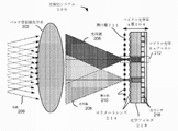
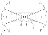
いくつかの実施形態では、距離測定を実行するための光学システムは、バルク送信器光学系、照明源、及び照明源とバルク送信器光学系との間に配設されたマイクロ光学チャネルアレイを含む。照明源は、バルク送信器光学系を通して個別の光ビームを光学システムの前方のフィールドに投射するように位置合わせされた複数の発光体を含む。マイクロ光学チャネルアレイは、複数のマイクロ光学チャネルを画定し、各マイクロ光学チャネルは、複数の発光体からの発光体から離れたマイクロ光学レンズを含み、マイクロ光学レンズが、発光体から光円錐を受信し、かつ発光体とバルク送信器光学系との間の場所で発光体から変位した焦点で発光体の縮小サイズのスポット画像を生成するように構成されている。各チャネルのマイクロ光学レンズは、発光体から光円錐を受信し、かつマイクロ光学レンズとバルク送信器光学系との間の焦点で発光体の縮小サイズの実スポット画像を生成するように構成されている。発光体からの光円錐の発散は、縮小サイズの実スポット画像を生成するためのマイクロ光学レンズの第2の光学面からの光円錐の発散より小さくすることができる。 In some embodiments, an optical system for performing range finding includes bulk transmitter optics, an illumination source, and a micro-optical channel array disposed between the illumination source and the bulk transmitter optics. . The illumination source includes a plurality of light emitters aligned to project individual beams of light through bulk transmitter optics into a field in front of the optical system. The micro-optical channel array defines a plurality of micro-optical channels, each micro-optical channel including a micro-optical lens remote from the emitters from the plurality of emitters, the micro-optical lens receiving cones of light from the emitters. and to produce a reduced size spot image of the light emitter at a location between the light emitter and the bulk transmitter optics at a focus displaced from the light emitter. Each channel's micro-optic lens is configured to receive a cone of light from the light emitter and produce a reduced size real spot image of the light emitter at a focal point between the micro-optic lens and the bulk transmitter optics. there is The divergence of the cone of light from the light emitter can be less than the divergence of the cone of light from the second optical surface of the micro-optical lens to produce a reduced size real spot image.
いくつかの追加の実施形態では、距離測定を実行するための光学システムは、発光システム及び光検出システムを含む。発光システムは、バルク送信器光学系と、バルク送信器光学系を通して個別の光ビームを光学システムの前方のフィールドに投射するように位置合わせされた複数の発光体を含む照明源と、照明源とバルク送信器光学系との間に配設されたマイクロ光学チャネルアレイと、を含む。マイクロ光学チャネルアレイは、複数のマイクロ光学チャネルを画定し、各マイクロ光学チャネルは、複数の発光体からの発光体から離れたマイクロ光学レンズを含み、マイクロ光学レンズが、発光体から光円錐を受信し、かつ発光体とバルク送信器光学系との間の場所で発光体から変位した焦点で発光体の縮小サイズのスポット画像を生成するように構成されている。光検出システムは、フィールドからの個別の光ビームを受信するように構成されたバルク受信器光学系と、フィールド内の複数の個別の非重複視野を画定する複数のマイクロ光学受信器チャネルを有する光学アセンブリと、を含む。光学アセンブリは、バルク受信器光学系の焦点面に沿って配置された複数の個別の開口部を有する開口層と、開口層の背後に配設された光センサのアレイと、開口層と光センサのアレイとの間に位置付けられた複数のレンズと、を含む。 In some additional embodiments, the optical system for performing range finding includes a light emitting system and a light detecting system. The light emitting system comprises bulk transmitter optics, an illumination source including a plurality of light emitters aligned to project individual light beams through the bulk transmitter optics into a field in front of the optical system, and an illumination source. and a micro-optical channel array disposed between the bulk transmitter optics. The micro-optical channel array defines a plurality of micro-optical channels, each micro-optical channel including a micro-optical lens remote from the emitters from the plurality of emitters, the micro-optical lens receiving cones of light from the emitters. and to produce a reduced size spot image of the light emitter at a location between the light emitter and the bulk transmitter optics at a focus displaced from the light emitter. The optical detection system has bulk receiver optics configured to receive separate light beams from the field and a plurality of micro-optical receiver channels defining a plurality of separate, non-overlapping fields of view within the field. including assembly; The optical assembly includes an aperture layer having a plurality of discrete apertures arranged along the focal plane of the bulk receiver optics, an array of photosensors disposed behind the aperture layer, and an aperture layer and the photosensors. and a plurality of lenses positioned between the array of .
特定の実施形態では、距離測定を実行するための光学システムは、光学的透明窓を有するハウジングと、ハウジング内に配設された光測距デバイスとを含む。光測距デバイスは、プラットフォームに結合された光送信器を含む。光送信器は、バルク送信器光学系、照明源、及び照明源とバルク送信器光学系との間に配設されたマイクロ光学チャネルアレイを含む。照明源は、バルク送信器光学系を通して個別の光ビームを光学システムの前方のフィールドに投射するように位置合わせされた複数の発光体を含む。マイクロ光学チャネルアレイは、照明源とバルク送信器光学系との間に配設されてもよく、マイクロ光学チャネルアレイは、複数のマイクロ光学チャネルを画定することができ、各マイクロ光学チャネルは、複数の発光体からの発光体から離れたマイクロ光学レンズを含むことができ、マイクロ光学レンズが、発光体から光円錐を受信し、かつ発光体とバルク送信器光学系との間の場所で発光体から変位した焦点で発光体の縮小サイズのスポット画像を生成するように構成されている。 In certain embodiments, an optical system for performing range finding includes a housing having an optically transparent window and an optical ranging device disposed within the housing. The optical ranging device includes an optical transmitter coupled to the platform. The optical transmitter includes bulk transmitter optics, an illumination source, and a micro-optical channel array disposed between the illumination source and the bulk transmitter optics. The illumination source includes a plurality of light emitters aligned to project individual beams of light through bulk transmitter optics into a field in front of the optical system. A micro-optical channel array may be disposed between the illumination source and the bulk transmitter optics, and the micro-optical channel array may define a plurality of micro-optical channels, each micro-optical channel comprising a plurality of a micro-optical lens remote from the emitter from the emitter, the micro-optical lens receiving a cone of light from the emitter and at a location between the emitter and the bulk transmitter optics is configured to generate a reduced size spot image of the light emitter at a focal point displaced from.
いくつかの実施形態では、光検出システムは、光学システムの外部のフィールドから発生する光線を受信するように構成されたバルク受信器光学系と、フィールド内の複数の個別の非重複視野を画定する複数のマイクロ光学受信器チャネルを有する光学アセンブリと、を含む。光学アセンブリは、バルク受信器光学系の焦点面に沿って配置された複数の個別の開口部を有する開口層と、開口層の背後に配設された光センサのアレイと、異なるマイクロ光学チャネルが異なる波長範囲を測定できるように構成された不均一光学フィルタ層と、を含む。不均一光学フィルタは、一次元で段階的に厚さが増加し、または各チャネルが一定の光学フィルタ層厚を有するように一次元で段階的に厚さが増加するが、異なるマイクロ光学チャネルの厚さが異なる段階的光学フィルタを含むことができる。 In some embodiments, the photodetection system defines a bulk receiver optic configured to receive light rays originating from a field external to the optical system and a plurality of separate non-overlapping fields of view within the field. an optical assembly having a plurality of micro-optical receiver channels. The optical assembly includes an aperture layer having a plurality of discrete apertures arranged along the focal plane of the bulk receiver optics, an array of optical sensors disposed behind the aperture layer, and different micro-optical channels. and a non-uniform optical filter layer configured to allow different wavelength ranges to be measured. The nonuniform optical filter has a stepwise thickness increase in one dimension, or a stepwise thickness increase in one dimension such that each channel has a constant optical filter layer thickness, but different micro-optical channels. Graduated optical filters with different thicknesses can be included.
いくつかの追加の実施形態では、光学システムは、光学システムの外部のフィールドからの光を受信するように構成されたバルク受信器光学系と、バルク光学系の背後に配設され、バルク光学系の焦点面に位置する複数の開口部を含む開口層と、焦点距離を有する複数のコリメートレンズを含むレンズ層であって、レンズ層が、開口層の背後に配設され、焦点距離によって開口層から分離される、レンズ層と、レンズ層の背後にある不均一光学フィルタ層と、複数の光センサを含む光センサ層と、を含む。開口層、レンズ層、不均一光学フィルタ層、及び光センサ層は、フィールド内の複数の個別の非重複視野を画定する複数のマイクロ光学チャネルを形成するように配置され、複数のマイクロ光学チャネル内の各マイクロ光学チャネルが、複数の開口部からの開口部、複数のレンズからのレンズ、フィルタ層からのフィルタ、及び複数の光センサからの光センサを含み、かつ、バルク受信器光学系からの入射光をマイクロ光学チャネルの光センサに伝達するように構成されている。不均一光学フィルタ層は、異なるマイクロ光学チャネルが異なる波長範囲を測定できるように構成されている。 In some additional embodiments, the optical system includes a bulk receiver optic configured to receive light from a field external to the optical system, and a bulk optic disposed behind the bulk optic and configured to receive light from a field external to the optical system. and a lens layer including a plurality of collimating lenses having a focal length, the lens layer disposed behind the aperture layer and the focal length of the aperture layer a lens layer, a non-uniform optical filter layer behind the lens layer, and a photosensor layer including a plurality of photosensors, separated from the lens layer; The aperture layer, the lens layer, the non-uniform optical filter layer, and the photosensor layer are arranged to form a plurality of micro-optical channels defining a plurality of distinct, non-overlapping fields of view within the field; each micro-optical channel of includes an aperture from the plurality of apertures, a lens from the plurality of lenses, a filter from the filter layer, and a photosensor from the plurality of photosensors, and from the bulk receiver optics It is configured to transmit incident light to the optical sensor of the micro-optical channel. The non-uniform optical filter layer is configured to allow different micro-optical channels to measure different wavelength ranges.
特定の実施形態では、光検出システムは、光学システムの外部のフィールドから発生する光線を受信するように構成されたバルク受信器光学系と、フィールド内の複数の個別の非重複視野を画定する複数のマイクロ光学受信器チャネルを有する光学アセンブリと、を含む。光学アセンブリは、プロセッサ、メモリ、及びASICで製造された複数の光センサを含むモノリシックASICと、バルク受信器光学系の焦点面に沿って配置された複数の個別の開口部を有する開口層であって、光センサのアレイが開口層の背後に配設されている、開口層と、開口層と光センサのアレイとの間に位置付けられた複数のレンズと、その構造全体に異なる中心波長を有して、少なくとも2つの異なるマイクロ光学受信器チャネルが異なる波長範囲の光を測定できるようにする不均一光学フィルタ層であって、開口層、複数のレンズ、及び不均一光学フィルタ層が、ASICのモノリシック構造の一部を形成するようにASIC上に形成される、不均一光学フィルタ層と、を含む。 In certain embodiments, the photodetection system includes a bulk receiver optic configured to receive light rays originating from a field external to the optical system, and a plurality of receiver optics defining a plurality of separate, non-overlapping fields of view within the field. an optical assembly having a micro-optical receiver channel of . The optical assembly is a monolithic ASIC containing a processor, memory, and multiple photosensors fabricated in the ASIC, and an aperture layer having multiple discrete apertures arranged along the focal plane of the bulk receiver optics. an aperture layer with an array of photosensors disposed behind the aperture layer; a plurality of lenses positioned between the aperture layer and the array of photosensors; to enable at least two different micro-optical receiver channels to measure light in different wavelength ranges, wherein the aperture layer, the plurality of lenses, and the non-uniform optical filter layer are integrated into the ASIC. a non-uniform optical filter layer formed on the ASIC to form part of the monolithic structure.
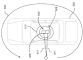
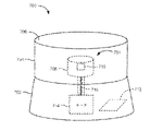
いくつかの実施形態では、距離測定を実行するための光学システムは、光学的透明窓を有するハウジングと、ハウジング内に配設された回転光測距デバイスと、ハウジング内に配設され、ハウジング内のプラットフォーム、光送信器、及び光受信器を含む光測距デバイスを回転させるように動作可能に結合されたモータと、ハウジング内に配設されたシステムコントローラであって、モータを制御し、光測距デバイスの光検出動作を開始及び停止するように構成されたシステムコントローラと、を含む。光測距デバイスは、プラットフォーム、プラットフォームに結合された光送信器、及びプラットフォームに結合された光受信器を含む。光送信器は、バルク送信器光学系及び複数の送信器チャネルを含み、各送信器チャネルが、狭帯域光を生成して、バルク送信器光学系を通して光学システムの外部のフィールドに送信するように構成された発光体を含む。光受信器は、バルク受信器光学系及び複数のマイクロ光学受信器チャネルを含み、各マイクロ光学チャネルが、バルク受信器光学系の焦点面と一致する開口部を含み、光学フィルタは、バルク受信器光学系からの光路に沿って位置付けられ、開口部と軸方向に位置合わせされ、光センサが、開口部及び光学フィルタを通過した入射光子に応答する。 In some embodiments, an optical system for performing range finding includes a housing having an optically transparent window; a rotating optical ranging device disposed within the housing; a motor operably coupled to rotate the optical ranging device including the platform of the, the optical transmitter, and the optical receiver; and a system controller disposed within the housing for controlling the motor and the optical a system controller configured to start and stop light sensing operations of the ranging device. The optical ranging device includes a platform, an optical transmitter coupled to the platform, and an optical receiver coupled to the platform. The optical transmitter includes bulk transmitter optics and a plurality of transmitter channels such that each transmitter channel produces narrowband light for transmission through the bulk transmitter optics into a field external to the optical system. Includes structured light emitters. The optical receiver includes bulk receiver optics and a plurality of micro-optical receiver channels, each micro-optical channel including an aperture coinciding with the focal plane of the bulk receiver optics; Positioned along the optical path from the optical system and axially aligned with the aperture, an optical sensor responds to incident photons that pass through the aperture and the optical filter.
いくつかの追加の実施形態では、距離測定を実行するための光学システムは、基部、上部、及び基部と上部との間に配設された光学的透明窓を有する固定ハウジングと、ハウジング内に配設され、光学的透明窓と位置合わせされた回転光測距デバイスと、ハウジング内に配設され、ハウジング内のプラットフォーム、光送信器、及び光受信器を含む光測距デバイスを回転させるように動作可能に結合されたモータと、ハウジング内に配設されたシステムコントローラであって、モータを制御し、光測距デバイスの光検出動作を開始及び停止するように構成されたシステムコントローラと、を含む。光測距デバイスは、プラットフォーム、プラットフォームに結合された光送信器、及びプラットフォームに結合された光受信器を含む。光送信器は、画像空間テレセントリックバルク送信器光学系及び複数の送信器チャネルを含み、各チャネルが、狭帯域光を生成して、バルク送信器光学系を通して光学システムの外部のフィールドに送信するように構成された発光体を含む。光受信器は、画像空間テレセントリックバルク受信器光学系及び複数のマイクロ光学受信器チャネルを含み、各マイクロ光学チャネルが、バルク受信器光学系の焦点面と一致する開口部を含み、開口部の背後のコリメートレンズ、コリメートレンズの背後の光学フィルタ、及び開口部を通過してコリメートレンズ及び光センサが、フィルタを通過した入射光子に応答する。 In some additional embodiments, an optical system for performing range finding includes a fixed housing having a base, a top, and an optically transparent window disposed between the base and the top; a rotating optical ranging device provided and aligned with the optically transparent window; and a rotating optical ranging device disposed within the housing to rotate the optical ranging device including a platform, an optical transmitter, and an optical receiver within the housing. a motor operably coupled; and a system controller disposed within the housing and configured to control the motor and to start and stop light sensing operations of the optical ranging device. include. The optical ranging device includes a platform, an optical transmitter coupled to the platform, and an optical receiver coupled to the platform. The optical transmitter includes image-space telecentric bulk transmitter optics and a plurality of transmitter channels, each channel for producing narrowband light for transmission through the bulk transmitter optics to a field external to the optical system. a light emitter configured to The optical receiver includes an image-space telecentric bulk receiver optic and a plurality of micro-optical receiver channels, each micro-optical channel including an aperture coinciding with the focal plane of the bulk receiver optic and behind the aperture. A collimating lens, an optical filter behind the collimating lens, and an aperture through the collimating lens and an optical sensor respond to incident photons passing through the filter.
特定の実施形態では、距離測定を実行するための光学システムは、基部、上部、及び基部と上部との間に配設された光学的透明窓を有する固定ハウジングと、ハウジング内に配設され、光学的透明窓と位置合わせされた光測距デバイスと、ハウジング内に配設され、ハウジング内の光測距デバイスを回転させるように動作可能に結合されたモータと、ハウジング内に配設されたシステムコントローラであって、モータを制御し、光測距デバイスの光検出動作を開始及び停止するように構成されたシステムコントローラと、を含む。光測距デバイスは、プラットフォーム、アレイ状に配置された複数の垂直キャビティ面発光レーザ(VCSEL)、及びプラットフォームに結合された光受信器を含む。複数のVCSELの各VCSELは、光の個別パルスを生成して光学システムの外部のフィールドに送信するように構成される。光受信器は、バルク受信器光学系、複数の光センサを含み、各光センサが、入射光子に応答する複数の単一光子アバランシェダイオード(SPAD)、及びバルク受信器光学系と複数の光センサとの間に配設された光学フィルタを含み、光の帯域がフィルタを通過して複数の光センサに到達する一方で、帯域の外の光が複数の光センサに到達するのを遮断するように構成される。 In certain embodiments, an optical system for performing distance measurements is disposed within a fixed housing having a base, a top, and an optically transparent window disposed between the base and the top; an optical ranging device aligned with the optically transparent window; a motor disposed within the housing and operably coupled to rotate the optical ranging device within the housing; a system controller configured to control the motor and to start and stop light sensing operations of the optical ranging device. The optical ranging device includes a platform, a plurality of vertical cavity surface emitting lasers (VCSELs) arranged in an array, and an optical receiver coupled to the platform. Each VCSEL of the plurality of VCSELs is configured to generate and transmit individual pulses of light into a field external to the optical system. The optical receiver includes bulk receiver optics, a plurality of photosensors, each photosensor a plurality of single-photon avalanche diodes (SPADs) responsive to incident photons, and the bulk receiver optics and the plurality of photosensors. such that a band of light passes through the filter to reach the plurality of photosensors, while blocking out-of-band light from reaching the plurality of photosensors. configured to
いくつかの実施形態では、距離測定を実行するための光学システムは、回転可能なプラットフォームと、回転可能なプラットフォームに結合され、バルク送信器光学系及び複数の送信器チャネルを含む光送信器と、回転可能なプラットフォームに結合され、バルク受信器光学系及び複数のマイクロ光学受信器チャネルを含む光受信器と、ハウジング内に配設され、プラットフォーム、光送信器、及び光受信器を回転させるように動作可能に結合されたモータと、光学システムの固定部品に取り付けられたシステムコントローラと、システムコントローラと光受信器との間に動作可能に結合され、システムコントローラが光受信器と通信できるようにする光通信リンクと、を含む。各送信器チャネルは、狭帯域光を生成して、バルク送信器光学系を通して光学システムの外部のフィールドに送信するように構成された発光体を含む。各マイクロ光学チャネルは、バルク受信器光学系の焦点面と一致する開口部を含み、光学フィルタは、バルク受信器光学系からの光路に沿って位置付けられ、開口部と軸方向に位置合わせされ、光センサが、開口部及びフィルタを通過した入射光子に応答する。光通信リンクは、光学システムの固定部品と回転可能なプラットフォームとの間に延びて、システムコントローラを光受信器に動作可能に結合することができる。光受信器は、開口部の背後にあり、光学フィルタに直接結合されたコリメートレンズを更に含むことができ、光学フィルタが、コリメートレンズの背後に位置付けられる。 In some embodiments, an optical system for performing range finding includes a rotatable platform, an optical transmitter coupled to the rotatable platform and including bulk transmitter optics and a plurality of transmitter channels; an optical receiver coupled to the rotatable platform and including bulk receiver optics and a plurality of micro-optical receiver channels; and disposed within the housing to rotate the platform, optical transmitter, and optical receiver. an operably coupled motor, a system controller attached to a fixed component of the optical system, and operably coupled between the system controller and the optical receiver to enable the system controller to communicate with the optical receiver. and an optical communication link. Each transmitter channel includes a light emitter configured to generate and transmit narrowband light through bulk transmitter optics into a field external to the optical system. each micro-optical channel includes an aperture coinciding with the focal plane of the bulk receiver optics, an optical filter positioned along the optical path from the bulk receiver optics and axially aligned with the aperture; A photosensor responds to incident photons that pass through the aperture and the filter. An optical communication link can extend between the fixed components of the optical system and the rotatable platform to operatively couple the system controller to the optical receiver. The optical receiver can further include a collimating lens behind the aperture and directly coupled to the optical filter, the optical filter positioned behind the collimating lens.
いくつかの追加の実施形態では、距離測定を実行するための光学システムは、回転可能なプラットフォームと、回転可能なプラットフォームに結合され、画像空間テレセントリックバルク送信器光学系及び複数の送信器チャネルを含む光送信器と、回転可能なプラットフォームに結合され、画像空間テレセントリックバルク受信器光学系及び複数のマイクロ光学受信器チャネルを含む光受信器と、ハウジング内に配設され、プラットフォーム、光送信器、及び光受信器を回転させるように動作可能に結合されたモータと、光学システムの固定部品に取り付けられたシステムコントローラと、システムコントローラと光受信器との間に動作可能に結合され、システムコントローラが光受信器と通信できるようにする光通信リンクと、を含む。各送信器チャネルは、狭帯域光を生成して、バルク送信器光学系を通して光学システムの外部のフィールドに送信するように構成された発光体を含む。各マイクロ光学チャネルは、バルク受信器光学系の焦点面と一致する開口部を含み、開口部の背後のコリメートレンズ、コリメートレンズの背後の光学フィルタ、及び開口部を通過してコリメートレンズ及び光センサが、フィルタを通過した入射光子に応答する。 In some additional embodiments, an optical system for performing range finding includes a rotatable platform and image space telecentric bulk transmitter optics and a plurality of transmitter channels coupled to the rotatable platform. an optical transmitter, an optical receiver coupled to a rotatable platform and including an image space telecentric bulk receiver optic and a plurality of micro-optical receiver channels; disposed within a housing comprising the platform, the optical transmitter, and a plurality of micro optical receiver channels; a motor operably coupled to rotate the optical receiver; a system controller attached to a fixed component of the optical system; and an optical communication link that allows communication with the receiver. Each transmitter channel includes a light emitter configured to generate and transmit narrowband light through bulk transmitter optics into a field external to the optical system. Each micro-optical channel includes an aperture coinciding with the focal plane of the bulk receiver optics, with a collimating lens behind the aperture, an optical filter behind the collimating lens, and a collimating lens and optical sensor through the aperture. responds to incident photons that pass through the filter.
特定の実施形態では、距離測定を実行するための光学システムは、回転可能なプラットフォームと、アレイ状に配置され、回転可能なプラットフォームに結合された複数の垂直キャビティ面発光レーザ(VCSEL)と、回転可能なプラットフォームに結合された光受信器と、ハウジング内に配設され、プラットフォーム、複数のVCSEL、及び光受信器を回転させるように動作可能に結合されたモータと、光学システムの固定部品に取り付けられたシステムコントローラと、システムコントローラと光受信器との間に動作可能に結合され、システムコントローラが光受信器と通信できるようにする光通信リンクと、を含む。複数のVCSELの各VCSELは、光の個別パルスを生成して光学システムの外部のフィールドに送信するように構成される。光受信器は、バルク受信器光学系及び複数の光センサを含み、各光センサが、入射光子に応答する複数の単一光子アバランシェダイオード(SPAD)を含む。 In certain embodiments, an optical system for performing range finding includes a rotatable platform, a plurality of vertical cavity surface emitting lasers (VCSELs) arranged in an array and coupled to the rotatable platform, and a rotating an optical receiver coupled to a possible platform; a motor disposed within the housing and operably coupled to rotate the platform, the plurality of VCSELs, and the optical receiver; and attached to a stationary component of the optical system. and an optical communication link operably coupled between the system controller and the optical receiver to enable the system controller to communicate with the optical receiver. Each VCSEL of the plurality of VCSELs is configured to generate and transmit individual pulses of light into a field external to the optical system. The optical receiver includes bulk receiver optics and a plurality of photosensors, each including a plurality of single-photon avalanche diodes (SPADs) responsive to incident photons.
いくつかの実施形態では、距離測定を実行するための光学システムは、バルク受信器光学系と、複数の開口部を含む開口層と、第1の複数のレンズを含む第1のレンズ層と、バルク受信器光学系を通過した後に光を受信し、放出の帯域を通過させる一方で、帯域の外の放出を遮断するように構成された光学フィルタ層と、複数の光センサを含む光センサ層と、を含み、各光センサは、光子を検出するように構成された複数の光検出器と、光センサで受信した入射光子を複数の光検出器に集束するように構成された第2の複数のレンズとを含む。光学システムは、複数の開口部からの開口部を含む複数の受信器チャネル内の各受信器チャネルを備えた複数の受信器チャネルと、複数の第1のレンズからのレンズと、光学フィルタ層からの光学フィルタと、各チャネルの開口部が、そのそれぞれのチャネルの個別の非重複視野を画定する、複数の光センサからの光センサと、を含む。複数の受信器チャネル内の各受信器チャネルについて、そのチャネルの光センサ内の複数の光検出器と第2の複数のレンズとの間に1対1の対応があってもよく、第2の複数のレンズのレンズの各々が、第2の複数のレンズの対応するレンズに光子を集束させるように構成されてもよい。 In some embodiments, an optical system for performing range finding includes bulk receiver optics, an aperture layer including a plurality of apertures, a first lens layer including a first plurality of lenses, an optical filter layer configured to receive light after passing through the bulk receiver optics and pass through a band of emissions while blocking out-of-band emissions; and a photosensor layer including a plurality of photosensors. and each photosensor includes a plurality of photodetectors configured to detect photons, and a second photodetector configured to focus incident photons received at the photosensor onto the plurality of photodetectors. a plurality of lenses; The optical system comprises a plurality of receiver channels with each receiver channel in the plurality of receiver channels including an aperture from the plurality of apertures, lenses from the plurality of first lenses, and an optical filter layer from the plurality of first lenses. and a photosensor from the plurality of photosensors, the aperture of each channel defining a separate, non-overlapping field of view for its respective channel. For each receiver channel in the plurality of receiver channels, there may be a one-to-one correspondence between the plurality of photodetectors in the photosensor of that channel and the second plurality of lenses; Each lens of the plurality of lenses may be configured to focus photons onto a corresponding lens of the second plurality of lenses.
いくつかの追加の実施形態では、距離測定を実行するための光学システムは、発光システム及び光検出システムを含む。発光システムは、バルク送信器光学系及び照明源を含む。照明源は、バルク送信器光学系を通して個別の光ビームを光学システムの前方のフィールドに投射するように位置合わせされた複数の発光体を含む。光検出システムは、バルク受信器光学系と、複数の開口部を含む開口層と、第1の複数のレンズを含む第1のレンズ層と、バルク受信器光学系を通過した後に光を受信し、放出の帯域を通過させる一方で、帯域の外の放出を遮断するように構成された光学フィルタ層と、複数の光センサを含む光センサ層と、を含む。各光センサは、光子を検出するように構成された複数の光検出器と、光センサで受信した入射光子を複数の光検出器に集束するように構成された第2の複数のレンズとを含む。光学システムは、複数の開口部からの開口部を含む複数の受信器チャネル内の各受信器チャネルを備えた複数の受信器チャネルと、複数の第1のレンズからのレンズと、光学フィルタ層からの光学フィルタと、各チャネルの開口部が、そのそれぞれのチャネルの個別の非重複視野を画定する、複数の光センサからの光センサと、を含む。 In some additional embodiments, the optical system for performing range finding includes a light emitting system and a light detecting system. A lighting system includes bulk transmitter optics and an illumination source. The illumination source includes a plurality of light emitters aligned to project individual beams of light through bulk transmitter optics into a field in front of the optical system. The light detection system receives light after passing through the bulk receiver optics, an aperture layer including a plurality of apertures, a first lens layer including a first plurality of lenses, and the bulk receiver optics. includes an optical filter layer configured to pass a band of emissions while blocking out-of-band emissions, and a photosensor layer including a plurality of photosensors. Each photosensor includes a plurality of photodetectors configured to detect photons and a second plurality of lenses configured to focus incident photons received at the photosensor onto the plurality of photodetectors. include. The optical system comprises a plurality of receiver channels with each receiver channel in the plurality of receiver channels including an aperture from the plurality of apertures, lenses from the plurality of first lenses, and an optical filter layer from the plurality of first lenses. and a photosensor from the plurality of photosensors, the aperture of each channel defining a separate, non-overlapping field of view for its respective channel.
特定の実施形態では、距離測定を実行するための光学システムは、光学的透明窓を有するハウジングと、ハウジング内に配設され、光学的透明窓と位置合わせされた光測距デバイスと、ハウジング内に配設され、ハウジング内のプラットフォーム、光送信器、及び光受信器を含む光測距デバイスを回転させるように動作可能に結合されたモータと、ハウジング内に配設されたシステムコントローラと、を含む。システムコントローラは、モータを制御し、光測距デバイスの光検出動作を開始及び停止するように構成される。光測距デバイスは、プラットフォーム、プラットフォームに結合された光送信器、プラットフォームに結合された光受信器を含む。光送信器は、バルク送信器光学系及び複数の送信器チャネルを含み、各送信器チャネルが、狭帯域光を生成して、バルク送信器光学系を通して光学システムの外部のフィールドに送信するように構成された発光体を含む。光受信器は、バルク受信器光学系と、複数の開口部を含む開口層と、第1の複数のレンズを含む第1のレンズ層と、バルク受信器光学系を通過した後に光を受信し、放出の帯域を通過させる一方で、帯域の外の放出を遮断するように構成された光学フィルタ層と、複数の光センサを含む光センサ層と、を含む。各光センサは、光子を検出するように構成された複数の光検出器と、光センサで受信した入射光子を複数の光検出器に集束するように構成された第2の複数のレンズとを含む。光学システムは、複数の開口部からの開口部を含む複数の受信器チャネル内の各受信器チャネルを備えた複数の受信器チャネルと、複数の第1のレンズからのレンズと、光学フィルタ層からの光学フィルタと、各チャネルの開口部が、そのそれぞれのチャネルの個別の非重複視野を画定する、複数の光センサからの光センサと、を含む。 In certain embodiments, an optical system for performing range finding includes a housing having an optically transparent window, an optical ranging device disposed within the housing and aligned with the optically transparent window, and a a motor disposed in and operably coupled to rotate an optical ranging device including a platform, an optical transmitter, and an optical receiver within a housing; and a system controller disposed within the housing. include. A system controller is configured to control the motor to start and stop light sensing operations of the optical ranging device. The optical ranging device includes a platform, an optical transmitter coupled to the platform, and an optical receiver coupled to the platform. The optical transmitter includes bulk transmitter optics and a plurality of transmitter channels such that each transmitter channel produces narrowband light for transmission through the bulk transmitter optics into a field external to the optical system. Includes structured light emitters. The optical receiver receives light after passing through the bulk receiver optics, an aperture layer including a plurality of apertures, a first lens layer including a first plurality of lenses, and the bulk receiver optics. includes an optical filter layer configured to pass a band of emissions while blocking out-of-band emissions, and a photosensor layer including a plurality of photosensors. Each photosensor includes a plurality of photodetectors configured to detect photons and a second plurality of lenses configured to focus incident photons received at the photosensor onto the plurality of photodetectors. include. The optical system comprises a plurality of receiver channels with each receiver channel in the plurality of receiver channels including an aperture from the plurality of apertures, lenses from the plurality of first lenses, and an optical filter layer from the plurality of first lenses. and a photosensor from the plurality of photosensors, the aperture of each channel defining a separate, non-overlapping field of view for its respective channel.
本開示の実施形態の性質及び利点のより良い理解は、以下の詳細な説明及び添付の図面を参照して得ることができる。 A better understanding of the nature and advantages of embodiments of the present disclosure may be obtained with reference to the following detailed description and accompanying drawings.
本開示のいくつかの実施形態は、フィールド内の周囲光及び/またはフィールド内の物体から反射した光送信器から放出された光から画像を生成できる光学撮像システムに関する。例えば、いくつかの実施形態では、光学撮像システムは、シーンまたは所与のエリアをアクティブに照明せず、代わりにシーンまたはエリア内の1または複数の物体から反射されるシーンまたはエリア内の周囲光を検出するパッシブシステムであり得る。パッシブ光学撮像装置システムには、フィールドの周囲光を受信するための光感知モジュールを含めることができる。光感知モジュールは、撮像情報を収集する広視野の狭帯域光学撮像システム(WFNBI)である。光感知モジュールは、1または複数のバルク受信器光学系、マイクロ光学受信器システム、及び光感知モジュールを操作するためのシステムコントローラを含むことができる。本開示のいくつかの実施形態によれば、マイクロ光学受信器システムは、1または複数のマイクロ光学受信器層と1または複数の光センサを含むことができ、各光センサは、受信光を測定できる1または複数の光検出器を含むことができる。 Some embodiments of the present disclosure relate to optical imaging systems capable of producing images from ambient light in a field and/or light emitted from an optical transmitter reflected from objects in the field. For example, in some embodiments, an optical imaging system does not actively illuminate a scene or a given area, but instead detects ambient light within a scene or area that is reflected from one or more objects within the scene or area. can be a passive system that detects A passive optical imager system may include a light sensing module for receiving ambient light in the field. The light sensing module is a wide field of view narrowband optical imaging system (WFNBI) that collects imaging information. The photo-sensing module can include one or more bulk receiver optics, a micro-optical receiver system, and a system controller for operating the photo-sensing module. According to some embodiments of the present disclosure, a micro-optic receiver system can include one or more micro-optic receiver layers and one or more optical sensors, each optical sensor measuring received light. It can include one or more photodetectors that can be used.
本明細書で定義されるバルク撮像光学系は、複数のレンズ素子を含み得る、1または複数の光学面とすることができ、1ミリメートルを超える明確な開口部を有し、投射された光を受信するように位置付けられ、または、受信光をマイクロ光学送信器/受信器層に焦点を合わせる。マイクロ光学送信器層などの発光体から受信した光を投射するバルク撮像光学系は、本明細書ではバルク送信器光学系または出力バルク撮像光学系と呼ばれることがある。マイクロ光学受信器など、フィールドから受信した光を光検出器に集束させるバルク光学層は、本明細書ではバルク受信器光学系または入力バルク撮像光学系と呼ばれることがある。入力画像空間テレセントリックバルク撮像光学系により、システムは広視野(FOV)にわたって狭帯域光を均一に測定できる。マイクロ光学受信器層には、マイクロ光学受信器チャネルの一次元または二次元アレイを含んでもよく、各マイクロ光学受信器チャネルは、1または複数の開口部、コリメートマイクロレンズ、光学フィルタ、及びと光センサを含む複数の構成要素を有する。場合によっては、マイクロ光受信器チャネル構造は、吸収性及び/または反射性の側壁及び/または集束漏斗を有するエンクロージャを備えた円柱状の構成を有する。マイクロ光学受信器チャネルは、以下で詳しく説明するように、開口部からの入射光線の収集を最大化し、光をコリメートして光学フィルタに垂直にし、隣接する開口部からの入力の混合による隣接するマイクロ光学受信器チャネルとのクロストークを最小限に抑える。様々な例において、本開示によるバルク撮像光学系は、発光体または光センサのアレイ全体の光または他の放出を修正する。マイクロ光学構造は、アレイの一部として含めることができ、アレイ内の異なる発光体及び/または光センサに対して光を異なる方法で修正できる。いくつかの実施形態では、個々のアレイ要素(光センサ及び/または発光体)ごとに1または複数のマイクロ光学要素が存在する。 Bulk imaging optics, as defined herein, can be one or more optical surfaces, which can include multiple lens elements, have a well-defined aperture greater than one millimeter, and direct projected light to Positioned to receive or focus received light onto a micro-optical transmitter/receiver layer. Bulk imaging optics that project light received from a light emitter, such as a micro-optic transmitter layer, are sometimes referred to herein as bulk transmitter optics or output bulk imaging optics. A bulk optical layer that focuses light received from a field onto a photodetector, such as a micro-optic receiver, is sometimes referred to herein as bulk receiver optics or input bulk imaging optics. The input image space telecentric bulk imaging optics allow the system to uniformly measure narrowband light over a wide field of view (FOV). The micro-optic receiver layer may include a one- or two-dimensional array of micro-optic receiver channels, each micro-optic receiver channel having one or more apertures, collimating microlenses, optical filters, and optical channels. It has multiple components including sensors. In some cases, the micro optical receiver channel structure has a cylindrical configuration with an enclosure having absorptive and/or reflective sidewalls and/or a focusing funnel. The micro-optical receiver channel maximizes the collection of incident rays from apertures, collimates the light perpendicular to the optical filter, and mixes input from adjacent apertures to adjacent Minimize crosstalk with micro-optical receiver channels. In various examples, bulk imaging optics according to the present disclosure modify light or other emissions across an array of light emitters or photosensors. Micro-optical structures can be included as part of an array and can modify light differently for different light emitters and/or photosensors within the array. In some embodiments, there are one or more micro-optical elements for each individual array element (photosensor and/or emitter).
いくつかの実施形態では、光学撮像システムは、フィールドに光を放出し、フィールド内の物体の表面で反射した後に放出光を検出できるアクティブシステムであり得る。アクティブ光学撮像システムは、光感知モジュールに加えて光送信モジュールを含むことができ、光測距デバイスとして構成できる。光送信モジュールには、個々の発光体のアレイで構成される送信器層を含んでもよく、各発光体は、光感知モジュール内の対応するマイクロ光学受信器チャネルと対にすることができ、個々の発光体と受信器チャネルとの間に特定の対にすることなく、シーン全体に均等に光を広げる均一な照明器とすることもできる。場合によっては、光送信モジュールは、発光体のアレイから出力される光を増強するためのマイクロ光学送信器チャネルアレイを含むことができる。動作中、発光体のアレイによって出力される光(例えば、レーザパルス)は、マイクロ光学送信器チャネルアレイを通過し、マイクロ光学送信器チャネルアレイからの光をよりよくキャプチャするために大きな開口数を有するバルク送信器光学系に入る。次に、光はバルク送信器光学系を出て、遠距離フィールドの複数のスポットを照明する。本明細書で更に詳細に説明するように、マイクロ光学送信器チャネルアレイは、バルク送信器光学系から発せられるビームの輝度を増強させ、スポット照明を増強すると同時に、測定画像の空間分解能を増強させることができる。 In some embodiments, the optical imaging system can be an active system that can emit light into a field and detect the emitted light after reflecting off surfaces of objects in the field. An active optical imaging system can include an optical transmission module in addition to an optical sensing module and can be configured as an optical ranging device. The light transmitting module may include a transmitter layer made up of an array of individual light emitters, each light emitter can be paired with a corresponding micro-optical receiver channel in the light sensing module, and an individual It can also be a uniform illuminator that spreads the light evenly across the scene without specific pairings between emitters and receiver channels. In some cases, the light transmitter module can include a micro-optical transmitter channel array for enhancing light output from the array of light emitters. In operation, light (e.g., laser pulses) output by the array of light emitters passes through the micro-optical transmitter channel array and has a large numerical aperture to better capture the light from the micro-optical transmitter channel array. into the bulk transmitter optics with The light then exits the bulk transmitter optics and illuminates multiple spots in the far field. As described in further detail herein, the micro-optical transmitter channel array enhances the brightness of the beam emitted from the bulk transmitter optics and enhances spot illumination while enhancing the spatial resolution of the measured image. be able to.
本開示のいくつかの実施形態によれば、撮像システムは、広視野の狭帯域光学システムである。したがって、撮像装置は画像をキャプチャし、少なくとも10度のFOV全体の光を検出できる。特定の実施形態では、撮像装置は、画像をキャプチャし、少なくとも20度のFOVにわたる光、及びいくつかの実施形態では少なくとも30度のFOVにわたる光を検出することができる。更に、撮像装置は約10nm以下の波長の光を検出できる。いくつかの特定の実施形態では、光感知モジュールは、約5nm以下の波長の光を検出することができる。いくつかの実施形態では、撮像システムは、約32度のFOVにわたって5nm未満の波長の検出光をキャプチャすることができる。FOVは、垂直方向または水平方向、またはその間のその他の角度にすることができる。 According to some embodiments of the present disclosure, the imaging system is a wide-field, narrow-band optical system. Accordingly, the imaging device can capture images and detect light over at least a 10 degree FOV. In certain embodiments, the imaging device is capable of capturing images and detecting light over at least 20 degrees FOV, and in some embodiments over at least 30 degrees FOV. Additionally, the imager can detect light at wavelengths of about 10 nm or less. In some particular embodiments, the light sensing module can detect light at wavelengths of about 5 nm or less. In some embodiments, the imaging system can capture detected light at wavelengths less than 5 nm over a FOV of about 32 degrees. The FOV can be vertical or horizontal, or any other angle in between.
本開示の実施形態によるパッシブ及びアクティブ光学撮像システムの機能及び構成をよりよく理解するために、それぞれを本明細書で詳細に説明する。 To better understand the function and configuration of passive and active optical imaging systems according to embodiments of the present disclosure, each is described herein in detail.
I.パッシブ光撮像装置システム
パッシブ光学撮像装置システムは、周囲光を受信して画像を生成する。図1は、本開示のいくつかの実施形態による、例示的なパッシブ光学撮像システム100のブロック図である。パッシブ光学撮像システム100は、フィールド内に存在する光をキャプチャするためのパッシブ光キャプチャデバイス102を含む。パッシブ光キャプチャデバイス102は、システムコントローラ104及び光感知モジュール106を含むことができる。撮像データは、パッシブ光撮像装置システム100が位置付けられているフィールドに存在する光を受信することにより、パッシブ光キャプチャデバイス102によって生成することができる。受信光は、システム100内の送信器から放出された光とは対照的に、フィールドに自然に存在する光、すなわち周囲光であり得る。
I. Passive Optical Imager Systems Passive optical imager systems receive ambient light to produce images. FIG. 1 is a block diagram of an exemplary passive
光感知モジュール106は、例えば、光センサの一次元または二次元アレイであり得るセンサアレイ108を含むことができる。各光センサ(単に「センサ」とも呼ばれるか、または当業者によって「ピクセル」と呼ばれることもある)は、例えばSPADなどの光検出器の集合体を含み得るか、またはセンサが単一の光子検出器(例えば、APD)であってもよい。光感知モジュール106は、光感知システム110を含み、センサアレイ108と一緒にされると、光検出システム112を形成することができる。いくつかの実施形態では、光感知システム110は、バルク受信器光学系114と、開口層、コリメートレンズ層、光学フィルタなどの光学部品116を含むことができ、センサアレイ108と組み合わせてマイクロ光学受信器チャネルのアレイを形成することができ、各マイクロ光学受信器チャネルは、システム100が位置付けられている周囲の視野の異なる視野内の画像ピクセルに対応する光を測定する。本開示によるマイクロ光学受信器チャネルの様々な実施形態のさらなる詳細は、以下の図17乃至図30に関連して詳細に議論される。
いくつかの実施形態では、光感知モジュール106のセンサアレイ108は、アレイ内の個々の光センサ(または光センサのグループ)からの測定光を処理するための光センサのアレイ、プロセッサ118、及び信号用メモリ120の両方を含む単一基板上のモノリシックデバイスの一部として(例えば、CMOS技術を使用して)製造される。センサアレイ108、プロセッサ118、及びメモリ120を含むモノリシック構造は、専用のASICとして製造することができる。いくつかの実施形態では、光学部品116は、センサアレイ108、プロセッサ118、及びメモリ120が一部であるモノリシック構造の一部とすることもできる。そのような場合、以下で更に説明するように、光学部品116を形成することができ、例えば、ASIC上でエポキシで(非可逆的に)接合し、ASICをモノリシック構造の一部とすることができる。上述のように、プロセッサ118(例えば、デジタル信号プロセッサ(DSP)、マイクロコントローラ、フィールドプログラマブルゲートアレイ(FPGA)など)及びメモリ120(例えば、SRAM)は、信号処理を実行することができる。信号処理の例として、光感知モジュール106のメモリ120は、各光センサまたは光センサのグループごとに、経時的に検出された光子を蓄積でき、これらの検出された光子はフィールドの画像を再現するために使用できる。
In some embodiments, the
いくつかの実施形態では、プロセッサ118からの出力は、さらなる処理のためにシステムコントローラ104に送られ、例えば、データはシステムコントローラ104の1または複数のエンコーダにより符号化され、その後データパケットとしてユーザインターフェース115に送られる。システムコントローラ104は、例えば、ASICまたはASICの一部としてのFPGAなどのプログラマブルロジックデバイスを使用することによる、メモリ124を有するプロセッサ122を使用することによる、及び上記の何らかの組み合わせを含む複数の方法で実現され得る。システムコントローラ104は、固定ベースコントローラと連携するか、またはベースコントローラとは独立して(事前にプログラムされた命令を介して)動作して、光検出の開始及び停止を含み、光検出器パラメータを調整するコマンドを送信することにより、光感知モジュール106を制御することができる。いくつかの実施形態では、システムコントローラ104は、光感知モジュール106とデータを交換するための1または複数の有線インターフェースまたはコネクタを有する。他の実施形態では、システムコントローラ104は、光通信リンクなどの無線相互接続を介して、光感知モジュール106と通信する。
In some embodiments, the output from
パッシブ光学撮像システム100は、ユーザがコンピュータシステム、例えばディスプレイ、タッチスクリーン、キーボード、マウス、及び/またはラップトップ、タブレット、及び/またはCPU及びメモリを含むハンドヘルドデバイスコンピューターシステムとインターフェースするためのトラックパッドと対話することを可能にするための任意の適切なユーザインターフェースであり得るユーザインターフェース115と対話することができる。ユーザインターフェース115は、パッシブ光学撮像システム100が取り付けられる物体に対してローカルであってもよいが、遠隔操作システムであってもよい。例えば、パッシブ光学撮像システム100への/からのコマンド及びデータは、セルラーネットワーク(LTEなど)、パーソナルエリアネットワーク(Bluetooth(登録商標)、Zigbeeなど)、ローカルエリアネットワーク(WiFi、IRなど)、またはインターネットなどの広域ネットワークを介してルーティングすることができる。
Passive
ハードウェア及びソフトウェアのユーザインターフェース115は、デバイスからの撮像データをユーザに提示できるが、ユーザが1または複数のコマンドでパッシブ光学撮像システム100を制御することも可能にし得る。コマンドの例には、撮像システムを作動させるまたは不作動にするコマンド、光検出器の露出レベル、バイアス、サンプリング期間、他の動作パラメータ(例えば、放出パルスパターン及び信号処理)を指定するコマンド、輝度などの発光体パラメータを指定するコマンドが含まれる。更に、結果を表示する方法をユーザが選択することを、コマンドで可能にすることができる。ユーザインターフェースは撮像システムの結果を表示することができ、これには、例えば、単一フレームのスナップショット画像、絶えず更新されるビデオ画像、及び/または一部またはすべてのピクセルについての他の光測定値の表示が含まれる。
A hardware and software user interface 115 can present imaging data from the device to the user, but may also allow the user to control the passive
本明細書で言及されるように、光感知システム110の1または複数の部品は、センサアレイ108、プロセッサ118、及びメモリ120を備えたモノリシック構造の一部であり得る。例えば、開口層、コリメートレンズ層、及び光学部品116の光学フィルタ層は、ダイシングの前後にウェハレベルで製造された複数のASICを有する半導体基板上に積み重ねられ、エポキシで接合され得る。例えば、光学フィルタ層は、光センサ層に対して置かれ、次いで光センサ層に接合されて光学フィルタ層を光センサ層と接合し、光学層がモノリシック構造の一部を形成する薄いウェハであり得る。コリメートレンズ層は、光学フィルタ層に射出成形できる。また、開口層は、透明基板の上に不透明基板を積層することにより、または透明基板に不透明フィルムをコーティングすることにより形成することができる。あるいは、光センサ層を製造してダイシングし、光学フィルタ層、コリメートレンズ層、及び開口層を製造してダイシングすることができる。次に、各ダイシングされた光センサ層と光学層を接合して、各モノリシック構造が光センサ層、光学フィルタ層、コリメートレンズ層、及び開口層を含むモノリシック構造を形成する。層をASICに接合することにより、ASICと接合層はモノリシック構造を形成できる。次いで、ウェハをデバイスにダイシングすることができ、各デバイスは、それぞれのバルク受信器光学系114と対にされて、光感知モジュール106を形成することができる。更に他の実施形態では、光感知モジュール106の1または複数の部品が、モノリシック構造の外側にあってもよい。例えば、開口層は、ピンホールを有する別個の金属シートとして実装されてもよい。本開示の一実施形態による光感知システム及びセンサアレイのより詳細な図は、図2に関して本明細書で説明される。
As referred to herein, one or more components of optical sensing system 110 may be part of a monolithic structure comprising
図2は、本開示のいくつかの実施形態による例示的な光検出システム200の簡略図である。光検出システム200は、図1に関して上述した光検出システム112を表すことができる。光検出システム200は、光感知システム及びセンサアレイを含むことができる。光感知システムは、バルク受信器光学系、開口層、コリメートレンズ層、及び光学フィルタ層を含むことができ、センサアレイは光センサのアレイを含むことができ、各光センサは光を測定するための1または複数の光検出器を含むことができる。いくつかの実施形態によれば、これらの部品は一緒に動作して、フィールドから光を受信する。例えば、光検出システム200は<5>バルク受信光学系</5>202とマイクロ光学受信器(Rx)層204を含むことができる。動作中、光線206は複数の方向からバルク受信器光学系202に入り、バルク受信器光学系202によって集束されて光円錐208を形成する。マイクロ光学受信器層204は、開口部210がバルク受信器光学系202の焦点面と一致するように位置付けられる。いくつかの実施形態では、マイクロ光学受信器層204は、マイクロ光学受信器チャネル212の一次元または二次元アレイであり得、各マイクロ光学受信器チャネル212は、光の流れの方向に同じ軸に沿って、例えば図2に示すように左から右に水平に位置付けられたそれぞれの開口部210、コリメートレンズ214、及び光センサ216から形成される。更に、各マイクロ光学受信器チャネル212は、本明細書で更に議論されるように、光センサ間の迷光からの干渉を軽減するための様々な方法で構成され得る。動作中、各マイクロ光学受信器チャネル212は、異なるピクセル(すなわち、フィールド内の位置)の光情報を測定する。
FIG. 2 is a simplified diagram of an exemplary
光線206は、バルク受信器光学系202の焦点で集束し、開口層211の開口部210を通過し、それぞれのコリメートレンズ214に入る。各コリメートレンズ214は、光線がすべてほぼ同じ角度で、例えば互いに平行に光学フィルタに入るように、受信光をコリメートする。バルク受信器光学系202の開口部と焦点距離は、開口部210で焦点を結ぶそれぞれの光線の円錐角を決定する。コリメートレンズ214の開口部サイズと焦点距離は、入射光線がどれだけ両行にコリメートできるかを決定し、これにより、光学フィルタ218でどの程度狭い帯域通過を実装できるかが決定される。開口部210は、光検出システム200の動作中に様々な機能を果たすことができる。例えば、開口部210は、(1)ピクセルFOVを制約して、光センサ平面のピッチが大きいにもかかわらず、狭い空間選択性を持たせ、(2)コリメートレンズの焦点面に小さな点状の光源を提供して、光線の厳密なコリメーションを達成でき、フィルタを通過する前に、コリメーションを改善すると、フィルタを通過できる帯域が狭くなり、(3)迷光を排除することができる。
Light rays 206 are focused at the focal point of
光学フィルタ218は、不要な波長の光を遮断する。干渉ベースのフィルタは、性能に強い角度依存性を示す傾向がある。例えば、0度の入射角で900nmの中心波長(CWL)を持つ1nm幅の帯域通過フィルタは、15度の入射角で898nmのCWLを有する場合がある。撮像システムは通常、この影響に対応するために幅数十ナノメートルのフィルタを使用するため、CWLのシフトは帯域通過幅よりもはるかに小さくなる。しかしながら、マイクロ光学層204の使用は、すべての光線がほぼ同じ入射角で光学フィルタ218に入ることを可能にし、したがって、CWLのシフトを最小限にし、非常にタイトなフィルタ(例えば10nm未満の幅)の使用を可能にする。光センサ216は、入射光子に応答して電流または電圧を生成する。いくつかの実施形態において、光学フィルタ218は、マイクロ光学受信器チャネル212のアレイ全体にわたって均一であるため、アレイ内の各個々のマイクロ光学受信器チャネル212は、同じ波長範囲の光を受信する。
The
いくつかの実施形態では、光センサ216は、光線206がコリメートレンズ214及び光学フィルタ218を最初に通過してから光センサ216に露出するように、コリメートレンズ214の反対側に位置付けられる。各光センサ216は、複数の単一光子アバランシェ検出器(SPAD)のミニアレイなどの複数の光検出器であってもよい。SPADのミニアレイのアレイは、単一のモノリシックチップ上に製造できるため、製造が簡素化される。いくつかの代替実施形態では、各光センサ216は、単一の光検出器、例えば標準フォトダイオード、アバランシェフォトダイオード、共振空洞フォトダイオード、または別の種類の光検出器であってもよい。
In some embodiments,
いくつかの他の実施形態では、光学フィルタ218は不均一である。例えば、段階的フィルタを使用すると、様々なマイクロ光学チャネルで様々な波長範囲を測定できる。言い換えると、段階的フィルタを使用すると、マイクロ光学チャネルのアレイ内の異なるマイクロ光学チャネルが異なる中心波長(CWL)を有することができる。段階フィルタは通常、一次元または二次元のいずれかで許容波長の範囲を徐々に変更する。ただし、段階的フィルタには、許容される波長の範囲が一次元または両方の次元で急速に(例えば、段階的に)変化するフィルタも含まれる。チャネルの様々なCWLは、様々な方法で作成できる。例えば、フィルタの厚さを変更したり、屈折率を変更したりできる。屈折率は、化学組成を修正するなど、フィルタ層を変更することによって、例えば不均一なドーピング濃度を持つように修正することによって変更できる。結果として、各チャネル(またはチャネルの行/列)は、異なるドーピング濃度を有する光学フィルタ層を有することができ、それにより、変更された厚さを有さずに各チャネル(またはチャネルの行/列)に対して異なるCWLをもたらす。段階的光学フィルタを使用してマイクロ光学チャネルの一次元アレイを回転させると、システムは各光センサの異なる波長の光を測定できる。段階的フィルタが走査の方向に沿って変化しているマイクロ光学チャネルの二次元アレイを走査すると、パッシブ光学撮像装置システムは空間内の各位置の複数の波長の光を測定できるが、そうするためには光センサの複数の光検出器を使用する。段階的フィルタを使用するこのような光学システムでは、同じ視野を持つ同じ光センサに対して異なる波長測定が行われるように、光センサのサンプリングの同期が必要である。多くの異なる波長を区別する撮像システムは、ハイパースペクトル撮像装置と呼ばれることもある。ハイパースペクトル撮像装置では、多くの場合、対象の波長の光をすべてほぼ同じ平面に集束させる必要がある。これは、色収差の影響を制限するように設計されたアクロマート、アポクロマート、スーパーアクロマート、または同様のレンズを使用することで達成できる。
In some other embodiments,
ハイパースペクトル撮像装置は、電磁スペクトル全体の複数の波長帯域から情報を収集する。波長帯域の絶対または相対強度は、化学物質濃度に関する情報を提供できる。例えば、特定の作物のクロロフィル含有量は、少数の波長帯域のみを使用して推定できる。同様の手法を使用して、貴重なミネラルを見つけ、毒素を識別したりできる。スペクトル情報は、歩行者、自動車、及び自動車環境で同様に遭遇する他の物体の分類を支援するためにも使用できる。 Hyperspectral imagers collect information from multiple wavelength bands across the electromagnetic spectrum. Absolute or relative intensities of wavelength bands can provide information about chemical concentration. For example, the chlorophyll content of a particular crop can be estimated using only a few wavelength bands. Similar techniques can be used to find valuable minerals, identify toxins, and more. Spectral information can also be used to aid in the classification of pedestrians, vehicles, and other objects similarly encountered in the automotive environment.
段階的減光フィルタは、フィルタ全体で空間的に変化する透過率を有するが、透過率は、特定の場所で波長にほとんど依存しない(例えば、青色光と同様に赤色光に対しても透過性がある)。走査型撮像システムでは、段階的減光フィルタを使用して、空間の同じポイントを様々な減衰度で撮像することができ、それにより、非段階的フィルタで達成できるよりも高いダイナミックレンジでの複合測定が可能になる。段階フィルタを備えたマイクロ光学受信器層のより良い理解は、図3A及び3Bを参照して達成することができる。 A graduated neutral density filter has a transmittance that varies spatially across the filter, but the transmittance is largely independent of wavelength at a particular location (e.g., it is permeable to red light as well as blue light). there is). In scanning imaging systems, a graduated neutral density filter can be used to image the same point in space with varying degrees of attenuation, thereby providing a composite image with a higher dynamic range than can be achieved with a non-gradual filter. measurement becomes possible. A better understanding of micro-optical receiver layers with graded filters can be achieved with reference to FIGS. 3A and 3B.
図3A及び図3Bは、本開示のいくつかの実施形態による、段階的フィルタ層を有するマイクロ光学受信器層の異なる実施形態の簡略図の斜視図である。具体的には、図3Aは、段階的フィルタ層302を備えたマイクロ光学受信器層300の簡略図の斜視図であり、図3Bは、段階的フィルタ層312を備えたマイクロ光学受信器層301の簡略図の斜視図である。図3A及び図3Bに示されるように、マイクロ光学受信器層300及び301はそれぞれ、2×2アレイとして二次元に配置された4つのマイクロ光学受信器チャネル304、306、308及び310を含む。図3A及び3Bは2×2アレイのみを有する実施形態を示しているが、当業者は、そのような実施形態が限定的ではなく、他の実施形態が任意の数のマイクロ光学受信器チャネルを有するように構成できることを理解する。これらの図において、フィルタ層302及び312の厚さ、及び縮尺通りに描かれていない周囲の層の厚さは、干渉フィルタ内の屈折材料の層の厚さとして解釈されるべきであることを理解されたい。これらの厚さが変化すると、干渉フィルタの特性(例えば、通過帯域CWL)が変化する。これらの実施形態は、ハイパースペクトルパッシブ光学撮像システムで使用することができる。
3A and 3B are perspective views of simplified schematics of different embodiments of micro-optic receiver layers with graded filter layers, according to some embodiments of the present disclosure. Specifically, FIG. 3A is a perspective view of a simplified schematic of a
図3A及び図3Bに示されるように、段階的フィルタ層302は、マイクロ光学受信器チャネルの複数の列にわたって一次元で徐々に増加する厚さを有し、段階的フィルタ層312は、各マイクロ光学受信器チャネルに対して一定の厚さを有する一次元で段階的に増加する厚さを有する。マイクロ光学受信器チャネル304及び308は、同じフィルタ厚を有し、同じ波長の光を検出する。マイクロ光学受信器チャネル306及び310は、同じフィルタ厚を有し、同じ波長の光を検出する。マイクロ光学受信器チャネル304及び308は、マイクロ光学受信器チャネル306及び310とは異なるフィルタ厚さを有することができ、したがって異なる波長の光を検出することができる。第1の時間間隔の間、マイクロ光学受信器チャネル304及び308は、それぞれ2つのピクセルの光の第1の波長の強度を測定する。いくつかの実施形態では、ハイパースペクトルパッシブ光学撮像システムは、第2の時間間隔中に、マイクロ光学受信器チャネル306及び310がそれぞれ同じ2つのピクセルの光の第2の波長の強度を測定するようにマイクロ光学受信器層を移動または回転させる。他の実施形態では、本開示によるハイパースペクトルパッシブ光学撮像装置システムは、固定マイクロ光学受信器層を含み、移動するターゲットを走査することができる。
As shown in FIGS. 3A and 3B, the graded
II.アクティブ光学撮像システム
本明細書で説明するように、光学撮像システムは、アクティブ光学撮像システムとして構成することもできる。アクティブ光学撮像装置システムは、アクティブ光学撮像装置システムがフィールドに独自の光を放出し、フィールド内の物体の表面で反射した後に放出光を検出するという点で、パッシブ光学撮像装置システムとは異なる。いくつかの実施形態では、アクティブな光学撮像装置システムは、放出及び受信された反射光を相関させて、放出光が反射された物体までの距離を決定できるLIDARデバイスとして利用できる。アクティブな光学撮像装置システムのより良い理解は、図4を参照して確認できる。
II. Active Optical Imaging System As described herein, the optical imaging system can also be configured as an active optical imaging system. Active optical imager systems differ from passive optical imager systems in that the active optical imager system emits its own light into a field and detects the emitted light after reflecting off the surfaces of objects in the field. In some embodiments, active optical imager systems can be utilized as LIDAR devices that can correlate emitted and received reflected light to determine the distance to an object from which the emitted light was reflected. A better understanding of the active optical imager system can be seen with reference to FIG.
図4は、本開示のいくつかの実施形態によるLIDARシステム400のブロック図を示している。LIDARシステム400は、光測距デバイス402及びユーザインターフェース415を含むことができる。光測距デバイス402は、測距システムコントローラ404、光送信(Tx)モジュール406、及び光感知(Rx)モジュール408を含む。1または複数の光パルス410を光送信モジュール406から光測距デバイス402を囲む視野内の物体に送信することにより、測距データが光測距デバイス402によって生成され得る。次いで、透過光の反射部分412が、いくらかの遅延時間の後、光感知モジュール408によって検出される。遅延時間に基づいて、反射面までの距離が決定され得る。例えば連続波、ドップラーなどの他の測距法も使用することができる。
FIG. 4 shows a block diagram of a
Txモジュール406は、発光体の一次元または二次元アレイであり得る発光体アレイ414と、発光体アレイ414と一緒になって発光システム438を形成できるTx光学システム416とを含む。Tx光学システム416は、画像空間テレセントリックであるバルク送信器光学系を含むことができる。いくつかの実施形態では、Tx光学システム416は、図11乃至図14に関して、及び/またはビーム成形、ビームステアリングなどに関して本明細書で議論されるように、バルク送信器光学系から発するビームの輝度を高める1または複数のマイクロ光学構造を更に含むことができる。発光体アレイ414または個々の発光体はレーザ源であり得る。Txモジュール406は、オプションのプロセッサ418及びメモリ420を更に含むことができるが、いくつかの実施形態では、これらのコンピューティングリソースは測距システムコントローラ404に組み込むことができる。いくつかの実施形態では、例えばバーカーコードなどのパルスコーディング技術を使用することができる。そのような場合、メモリ420は、光をいつ送信すべきかを示すパルスコードを格納することができる。一実施形態では、パルスコードは、メモリに格納された整数のシーケンスとして格納される。
Tx module 406 includes
光感知モジュール408は、図1に関して本明細書で説明した光感知モジュール106と構造が実質的に同様であり得る。したがって、プロセッサ422、メモリ424、センサアレイ426、及びRx光学システム428の詳細(センサアレイ426と一緒に光検出システム436を形成できる場合)は、図1に関して本明細書で参照することができ、これらの部品に関しては、簡潔にするためにここで説明する。LIDARシステム400の場合、センサアレイ426の各センサ(例えば、SPADの集合体)は、例えば、光感知モジュール408及び光送信モジュール406の幾何学的構成の結果として、発光体アレイ414の特定の発光体に対応し得る。例えば、いくつかの実施形態では、発光体アレイ414は、バルク送信器光学系の焦点面に沿って配置することができ、バルク送信器光学系からシステムの前方のフィールドに投射される各照明ビームは、システムから初期閾値距離を超えた任意の距離で、対応する受信器チャネルの視野と実質的に同じサイズと形状になる。
Photo-sensing
いくつかの実施形態では、プロセッサ418は、アレイ内の個々の光子検出器(または検出器のグループ)からの生のヒストグラムの信号処理を実行することができる。信号処理の例として、各光子検出器、または各光子検出器のグループに、メモリ424(例えば、SRAM)は、連続する時間ビンにわたって検出された光子のカウントを累積することができ、これらの時間ビンを組み合わせて使用して、反射光パルスの時系列(すなわち、光子のカウント対時間)を再作成することができる。集計された光子カウントのこの時系列は、本明細書では強度ヒストグラム(または単にヒストグラム)と称される。プロセッサ418は、整合フィルタとピーク検出処理とを実装して、適時に戻り信号を識別することができる。更に、プロセッサ418は、SPADの飽和及び消光に起因して起こり得るパルス形状歪みの影響を受けにくい光子時系列を回復するのに役立つ、マルチプロファイル整合フィルタリングなどの特定の信号処理技術を(例えば、プロセッサ422によって)完遂することができる。いくつかの実施形態では、そのようなフィルタリングのすべてまたは一部は、FPGAで具体化され得るプロセッサ458によって実行され得る。
In some embodiments,
いくつかの実施形態では、プロセッサ418からの光子時系列は、さらなる処理のために測距システムコントローラ404に送られ、例えば、データは測距システムコントローラ404の1または複数のエンコーダにより符号化され、その後データパケットとしてユーザインターフェース415に送られる。測距システムコントローラ404は、例えば、ASICまたはASICの一部としてのFPGAなどのプログラマブルロジックデバイスを使用することによる、メモリ432を有するプロセッサ430を使用することによる、及び上記の何らかの組み合わせを含む複数の方法で実現され得る。測距システムコントローラ404は、固定ベースコントローラと連携するか、またはベースコントローラとは独立して(事前にプログラムされた命令を介して)動作して、光検出の開始及び停止を含み、光検出器パラメータを調整するコマンドを送信することにより、光感知モジュール408を制御することができる。同様に、測距システムコントローラ404は、発光開始及び停止制御、ならびに他の発光体パラメータ(例えば、パルスコード)を調整し得る制御を含むコマンドを送信するか、またはベースコントローラからのコマンドを中継することにより、光送信モジュール406を制御することができる。いくつかの実施形態では、測距システムコントローラ404は、光感知モジュール408及び光送信モジュール406とデータを交換するための1または複数の有線インターフェースまたはコネクタを有する。他の実施形態では、測距システムコントローラ404は、光通信リンクなどの無線相互接続を介して、光感知モジュール408及び光送信モジュール406と通信する。
In some embodiments, the photon time series from
光測距デバイス402は、固定及び走査アーキテクチャの両方で使用することができる。電気モータ434は、走査LIDARアーキテクチャの一部として、Txモジュール406及びRxモジュール408などのシステム構成要素を回転させるために使用できるLIDARシステム400のオプションの構成要素である。システムコントローラ404は、スキャンLIDARシステムを実装するために必要に応じて、電気モータ434を制御し、回転を開始し、回転を停止し、回転速度を変えることができる。例示的な固定LIDARデバイスは、図5A及び図5Bに関して以下で説明され、一方、例示的な走査LIDARデバイスは、図6A、図6B及び図7に関して本明細書で更に説明される。
Optical ranging device 402 can be used in both fixed and scanning architectures.
LIDARシステム400は、ユーザインターフェース415の1または複数のインスタンス化と相互作用することができる。異なるインスタンス化は変化する場合があり、モニタ、キーボード、マウス、CPU及びメモリを備えたコンピュータシステム、自動車またはその他の車両のタッチスクリーン、タッチスクリーンを有するハンドヘルドデバイス、またはその他の適切なユーザインターフェースを含み得るが、これらに限定されない。ユーザインターフェース415は、LIDARシステム400が取り付けられる物体に対してローカルであってもよいが、遠隔操作システムであってもよい。例えば、LIDARシステム400への、またはLIDARシステム400からのコマンド及びデータは、セルラーネットワーク(LTEなど)、パーソナルエリアネットワーク(Bluetooth(登録商標)、Zigbeeなど)、ローカルエリアネットワーク(WiFi、IRなど)、またはインターネットなどの広域ネットワークを介してルーティングすることができる。
ハードウェア及びソフトウェアのユーザインターフェース415は、デバイスからのLIDARデータをユーザに提示できるが、ユーザが1または複数のコマンドでLIDARシステム400を制御することも可能にし得る。コマンドの例には、LIDARシステムを作動させるまたは不作動にするコマンド、光検出器の露出レベル、バイアス、サンプリング期間、他の動作パラメータ(例えば、放出パルスパターン及び信号処理)を指定するコマンド、輝度などの発光体パラメータを指定するコマンドが含まれる。更に、結果を表示する方法をユーザが選択することを、コマンドで可能にすることができる。ユーザインターフェースはLIDARシステムの結果を表示することができ、これには、例えば、単一フレームのスナップショット画像、絶えず更新されるビデオ画像、及び/または一部またはすべてのピクセルについての他の光測定値の表示が含まれる。いくつかの実施形態では、ユーザインターフェース415は、車両からの物体の距離(近接性)を追跡し、場合によっては運転者に警告を提供したり、運転者の行動の分析のためにそのような追跡情報を提供したりすることができる。
A hardware and software user interface 415 can present LIDAR data from the device to the user, but may also allow the user to control the
いくつかの実施形態では、例えば、LIDARシステム400が車両ナビゲーションに使用される場合、ユーザインターフェース415は、出力を受信するか、車両制御ユニットの一部であり得、そうでなければ、上記の有線または無線ネットワークのいずれか1つなどのネットワークを介して光測距デバイス402及び/またはユーザインターフェース415と通信する、車両の制御に関連する1または複数のパラメータは、受信したLIDARデータに基づいて車両制御ユニットによって修正できる。例えば、完全自律走行車両では、LIDARシステム400は、GPS及び他のデータと連携してナビゲーションを支援するために、車を取り巻く環境のリアルタイム3D画像を提供できる。他の場合には、LIDARシステム400は、先進運転支援システム(ADAS)の一部として、または、例えば、アダプティブクルーズコントロール、自動駐車、運転者の眠気監視、死角監視、衝突回避システムなどの任意の数の異なるシステムに3D撮像データを提供できる安全システムの一部として、使用され得る。ユーザインターフェース415が車両制御ユニットの一部として実装される場合、運転者に警告を提供することができるか、または物体のトラッキングを追跡することができる。
In some embodiments, for example, if the
A.固体アーキテクチャ
本開示のいくつかの実施形態によれば、LIDARシステムは、固定アーキテクチャを有する固体LIDARシステムとして構成され得る。そのようなLIDARシステムは回転せず、したがって、センサ及び送信器モジュールを回転させるために、例えば図4の電気モータ434などの別個のモータを必要としない。固体LIDARシステムの例を図5A及び図5Bに示す。
A. Solid-State Architecture According to some embodiments of the present disclosure, a LIDAR system may be configured as a solid-state LIDAR system with a fixed architecture. Such a LIDAR system does not rotate and therefore does not require a separate motor, such as
図5A及び図5Bは、固体LIDARシステムの例示的な実装態様の簡単な図である。具体的には、図5Aは、本開示のいくつかの実施形態による、自動車などの道路車両505の外側領域に固体LIDARシステム502a~dが実装される実装態様500を示す。図5Bは、本開示のいくつかの実施形態による、固体LIDARシステム504a~bが道路車両505の上部に実装される実装態様501を示す図である。各実装態様では、LIDARシステムの数、LIDARシステムの配置、及び各LIDARシステムの視野は、全体ではないにしても、車両を囲む環境の360度の視野の大部分を取得できる。LIDARシステムの自動車実装態様は、本明細書では単に説明のために選択したものであり、本明細書で説明されるセンサは、例えば、ボート、航空機、列車などの他の種類の車両で、ならびに医用撮像、携帯電話、拡張現実、測地学、ジオマティクス、考古学、地理学、地質学、地形学、地震学、林業、大気物理学、レーザ誘導、空中レーザスワスマッピング(ALSM)、レーザ高度計などの、3D深度画像が有用な様々な他の用途で、利用され得る。
5A and 5B are simple diagrams of exemplary implementations of solid-state LIDAR systems. Specifically, FIG. 5A shows an
図5Aを参照すると、固体LIDARシステム502a~dは、車両の外側領域、フロント及びバックフェンダーの近くに取り付けることができる。LIDARシステム502a~dはそれぞれ、車両505の最も外側のコーナーの近くに位置付けられるように、車両505のそれぞれのコーナーに位置付けることができる。そのようにして、LIDARシステム502a~dは、領域506a~dのフィールド内の物体からの車両505の距離をより良く測定することができる。各固体LIDARユニットは、各ユニットがそれ自体でキャプチャできるよりも大きい複合視野をキャプチャできるように、異なる方向を(おそらくユニット間で部分的に重複する及び/または非重複の視野を有して)向くことができる。シーン内の物体は、LIDAR Txモジュール508から放出される光パルス510の部分を反射することができる。次いで、光パルス510の1または複数の反射部分512は、LIDARシステム502aに戻り、Rxモジュール509により受信され得る。Rxモジュール509は、Txモジュール508と同じハウジングに配設することができる。
Referring to FIG. 5A, solid-
図5Aは、車両の四隅に取り付けられた4つの固体LIDARシステムを示しているが、実施形態はそのような構成に限定されない。他の実施形態は、車両の他の領域に搭載されたより少ないまたはより多い固体LIDARシステムを有することができる。例えば、図5Bに示すように、LIDARシステムは車両505の屋根に取り付けることができる。そのような実施形態では、LIDARシステムは、車両505の周囲の領域506a~dをより良く観察するためにより高い視点を有することができる。
Although FIG. 5A shows four solid-state LIDAR systems mounted at four corners of a vehicle, embodiments are not limited to such a configuration. Other embodiments may have fewer or more solid state LIDAR systems mounted in other areas of the vehicle. For example, the LIDAR system can be mounted on the roof of a
B.走査アーキテクチャ
いくつかの実施形態では、本開示によるLIDARシステムは、LIDARシステムが360度未満の角度の間で振動する走査アーキテクチャを採用することができる。例えば、図5Bの実装態様501のLIDARシステム504a~bはそれぞれ、例えば視野506aと506bとの間の領域514、及び視野506cと506dとの間の領域516で、車両505の前及び/または背後のシーン全体を走査するために走査アーキテクチャを使用することができる。走査LIDARシステムに位置する1または複数の光源(図示せず、赤外線、近赤外線、紫外線、可視光、例えば緑色レーザ波長スペクトルなどのLIDARシステムに適した波長スペクトルのレーザを含むがこれに限定されない、放射を放出ための様々な異なる適切な光源であり得る)の出力ビームを光のパルスとして出力し、走査して、例えば360度未満の角度で回転させて、車両の周囲のシーンを照明することができる。いくつかの実施形態では、回転矢印514及び516によって表される走査は、機械的手段、例えば、発光体を回転柱または回転プラットフォームに取り付けることによって実施することができる。例えば、デジタルマイクロミラー(DMD)デバイス、デジタル光処理(DLP)デバイスなどの1または複数のMEMSベースの反射器を使用するマイクロチップを使用するなど、チップベースのビームステアリング技術を使用することもできる。いくつかの実施形態では、スキャンは、非機械的手段を介して、例えば、電子信号を使用して1または複数の光フェーズドアレイを操縦することにより達成することができる。
B. Scanning Architecture In some embodiments, a LIDAR system according to the present disclosure may employ a scanning architecture in which the LIDAR system oscillates between angles of less than 360 degrees. For example, the
他の実施形態は、車両を取り巻く環境の360度全体を走査する走査アーキテクチャを実装することができる。そのような走査LIDARシステムは、時計回りまたは反時計回りの方向に360度連続的に繰り返し回転することができ、したがって、別個のモータ、例えば図4の電気モータ434を利用して、センサ及び送信器モジュールを回転させることができる。例示的な回転式LIDARシステムを図6A及び図6Bに示す。
Other embodiments may implement a scanning architecture that scans the entire 360 degrees of the environment surrounding the vehicle. Such a scanning LIDAR system can rotate continuously and repeatedly through 360 degrees in a clockwise or counterclockwise direction, thus utilizing separate motors, such as
図6Aは、本開示のいくつかの実施形態による、自動車などの車両605用に実装され、連続的な360度走査が可能な例示的な走査LIDARシステム600の簡略図のトップダウン図である。例えば、LIDARシステム600内に位置付けられた1または複数の光源(赤外線または近赤外線パルスIRレーザなど、図示せず)の出力ビームは、車両の周りのシーン620を照明するために走査、例えば回転され得る。いくつかの実施形態では、回転矢印615によって表される走査は、図5Bに関して本明細書で説明する任意の適切な機械的手段、例えば、発光体を回転柱またはプラットフォームに取り付けること、または、検流計やチップベースのステアリング技術の使用などの任意の他の機械的手段によって実施することができる。動作中、任意の方向及びLIDARシステム600のビュー内の車両605の周囲の物体は、LIDARシステム600の送信モジュール608から放出される光パルス611の一部を反射することができる。次に、光パルス611の1または複数の反射部分617がLIDARシステム600に戻り、その感知モジュール609によって検出することができる。場合によっては、感知モジュール609は、送信モジュール608と同じハウジングに配設することができる。
FIG. 6A is a simplified top-down view of an exemplary
図6Aは、車両605の屋根に取り付けられた固体LIDARシステムを示しているが、実施形態はそのような構成に限定されない。他の実施形態は、車両の他の領域に取り付けられた固体LIDARシステムを有することができる。例えば、LIDARシステムは、図6Bに示すように、車両のコーナーに取り付けることができる。図6Bは、本開示のいくつかの実施形態による、固体LIDARシステム604a~dが、自動車などの路上走行車の外側領域に実装される実装態様601を示す。この実装態様では、各LIDARシステム604a~dは、360度全体の距離を測定できる回転式LIDARシステムであり得る。しかしながら、これらの測定値の少なくともいくつかは車両605に関して測定されるため、これらの測定値は無視することができる。したがって、各LIDARシステム605a~dは、360度の走査からの測定値のサブセットのみを利用することができ、例えば、車両605をキャプチャしない領域619a~dをカバーする角度のみが利用される。
Although FIG. 6A shows a solid-state LIDAR system mounted on the roof of a
図7は、本開示のいくつかの実施形態による、360走査アーキテクチャを採用するLIDARシステム700の簡略化された例示的な斜視図である。いくつかの実施形態では、LIDARシステム700は、時計回りまたは反時計回りの方向に回転して車両の周囲のフィールドを観察する光測距デバイス701を含むことができる。システム700は、固定ハウジング702、光学的透明窓704、及びLIDARシステム700の内部部品の保護を提供する固定蓋706を含むことができる。窓704は、円筒形状を有するように構成することができる固定ハウジング702の周囲に完全に延びることができる。システム700の内部部品は、回転プラットフォーム708と、回転プラットフォーム708に取り付けられた感知及び送信モジュール710とを含み得る光測距デバイス701を含むことができる。いくつかの実施形態では、光測距デバイス701は、モジュール710が窓704を介して光を放出及び受信するように位置付けられ、放出光が固定ハウジング702または固定蓋706に放出されないように窓704と位置合わせされる。例えば、位置合わせされた位置では、光測距デバイス701の水平方向の中心は窓704の水平方向の中心と一致する。感知及び送信モジュール710は、例えば、光感知モジュール408及び光送信モジュール406であり得、任意選択で、マイクロ光学層を冷却するヒートシンク(図示せず)を含み得る。LIDARシステム700はまた、固定ハウジング702内にあるシステムコントローラ712(例えば、コントローラ404)及び電気モータ714(例えば、モータ434)を含むことができる。電気モータ714は、プラットフォーム708を回転させ、それにより、感知及び送信モジュール710を、例えば時計回りまたは反時計回り方向に360度連続して回転するように回転させる。システムコントローラ712は、光通信リンク716を使用して感知及び送信モジュール710と通信することができる。光通信リンク716により、感知及び送信モジュール710は、固定ハウジング702に機械的に結合され、プラットフォーム708とともに回転しない固定システムコントローラ712と、機械的摩耗及び破損なしに光通信リンク716を介して通信できる。いくつかの実施形態では、システムコントローラ712は、モータを制御し、LIDARシステム700の光検出動作を開始及び停止することができる。システムコントローラ712は、平行関係に配置された2つ以上の積み重ねられた平面回路基板を含むことができ、これは、弁護士ドケット番号103033-P010US1-1073278「Compact Lidar System」という名称の共有及び同時出願の特許出願で詳細に議論されており、あらゆる目的のためにその全体が参照により本明細書に組み込まれる。
FIG. 7 is a simplified exemplary perspective view of a
III.アクティブ撮像システムの動作
図8は、いくつかの実施形態による、光測距システムの光送信及び検出プロセスの例示的な一実施例を示す。図8は、システムを囲む容積またはシーンの3次元距離データを収集する光測距システム800(例えば、固体型もしくは、及び/または走査型)を示す。図8は、発光体とセンサとの間の関係を強調する理想化された図であり、したがって、他のコンポーネントは示されていない。
III. Operation of an Active Imaging System FIG. 8 shows an illustrative example of the optical transmission and detection process of an optical ranging system, according to some embodiments. FIG. 8 shows an optical ranging system 800 (eg, solid-state and/or scanning) that collects three-dimensional range data of a volume or scene surrounding the system. FIG. 8 is an idealized diagram highlighting the relationship between the light emitter and the sensor, thus other components are not shown.
光測距システム800は、発光体アレイ810と光センサアレイ820とを含む。発光体アレイ810は、発光体812及び発光体816などの発光体のアレイ、例えば、垂直キャビティ面発光レーザ(VCSEL)などのアレイを含む。光センサアレイ820は、例えばセンサ822及び826などの光センサのアレイを含む。光センサは、各光センサに対して、単一光子アバランシェダイオード(SPAD)などの個別の光検出器のセットを使用するピクセル化照明センサであってもよい。しかしながら、様々な実施形態は、任意の種類の光子センサを配置することができる。
Optical ranging
各発光体は、隣接する発光体からわずかにオフセットされ得、かつ隣接する発光体から異なる視野内に光パルスを送信するように構成され得るため、その発光体のみに関連付けられたそれぞれの視野を照明することができる。例えば、発光体812は、(1または複数の光パルスから形成された)照明ビーム814を円形視野832(そのサイズは明確にするために誇張されている)内に放出する。同様に、発光体816は、照明ビーム818(発光体チャネルとも呼ばれる)を円形視野834内に放出する。複雑さを避けるために図8には示されていないが、各発光体は対応する視野内に対応する照明ビームを放出し、結果として2Dの視野のアレイが照明される(この例では21個の異なる視野)。
Each light emitter can be slightly offset from adjacent light emitters and can be configured to transmit light pulses in different fields of view from adjacent light emitters, thus limiting the respective field of view associated with that emitter only. can be illuminated. For example,
発光体によって照明される各視野は、測距データから生成される対応する3D画像内のピクセルまたはスポットと考えられ得る。各発光体チャネルは、各発光体に個別で、他の発光体チャネルと非重複とすることができる、つまり、発光体のセットと非重複フィールドまたはビューのセットとの間に1対1のマッピングがある。したがって、図8の実施例では、システムは3D空間で21個の異なるポイントをサンプリングし得る。より高密度の発光体アレイを有することにより、または1つの発光体が空間内の複数のポイントをサンプリングできるように、発光体ビームの角度位置を経時的にスキャンすることにより、ポイントの高密度サンプリングを実現することができる。上記のように、スキャンは、発光体/センサアセンブリ全体を回転させることにより実行できる。 Each field of view illuminated by a light emitter can be considered a pixel or spot in the corresponding 3D image generated from the ranging data. Each emitter channel can be individual to each emitter and non-overlapping with other emitter channels, i.e. a one-to-one mapping between a set of emitters and a non-overlapping set of fields or views. There is Thus, in the example of FIG. 8, the system can sample 21 different points in 3D space. Dense sampling of points by having a higher density of emitter arrays or by scanning the angular position of the emitter beam over time so that one emitter can sample multiple points in space can be realized. As noted above, scanning can be performed by rotating the entire emitter/sensor assembly.
各センサは、上述の発光体のように、隣接するセンサからわずかにオフセットすることができ、各センサはセンサの前のシーンの異なる視野を見ることができる。更に、各センサの視野は、例えば、それぞれの発光体チャネルの視野と実質的に一致し、例えば重なり合い、同じサイズである。 Each sensor can be slightly offset from adjacent sensors, like the illuminators described above, allowing each sensor to see a different view of the scene in front of the sensor. Further, the field of view of each sensor may, for example, substantially match, eg, overlap, and be the same size as the field of view of the respective emitter channel.
図8において、対応する発光体-受信器チャネル間の距離は、視野内の物体までの距離に対して誇張されている。実際には、わずかなフィールド内の物体までの距離は、対応する発光体-受信器チャネル間の距離よりはるかに大きいため、発光体から物体までの光の経路は、物体からセンサまで戻る反射光の経路にほぼ平行である(すなわち、光はほとんど「後方反射」される)。したがって、システム800の前には、個々のセンサの視野と個々の発光体の視野とが重なる距離の範囲がある。
In FIG. 8, the corresponding emitter-receiver channel distances are exaggerated with respect to the distances to objects in the field of view. In practice, the distance to an object in a small field is much larger than the corresponding emitter-receiver channel distance, so the path of light from the emitter to the object is the reflected light from the object back to the sensor. (ie, the light is mostly "back-reflected"). Thus, in front of
発光体の視野はそれぞれのセンサの視野と重なっているため、各受信器チャネルは理想的には、それぞれの発光体チャネルを起源とし、理想的にはクロストークのない反射照明ビームを検出できる、つまり、他の照明ビームからの反射光は検出されない。したがって、各光センサは、それぞれの光源に対応し得る。例えば、発光体812は照明ビーム814を円形視野832内に放出し、照明ビームの一部は物体830から反射する。理想的には、反射ビーム824はセンサ822のみによって検出される。したがって、発光体812及びセンサ822は同じ視野、例えば視野832を共有し、発光体-センサ対を形成する。同様に、発光体816及びセンサ826は発光体-センサ対を形成し、視野834を共有する。図8では発光体-センサ対は、それぞれのアレイ内の同じ相対位置にあるものとして示されているが、システムで使用される光学系の設計に応じて、任意の発光体を任意のセンサと対にすることができる。
Since the field of view of the emitters overlaps the field of view of the respective sensor, each receiver channel can ideally detect the reflected illumination beam originating from its respective emitter channel, ideally without crosstalk. That is, reflected light from other illumination beams is not detected. Accordingly, each photosensor may correspond to a respective light source. For example,
測距測定中、LIDARシステムを取り巻く容積の周りに分布する様々な視野からの反射光が様々なセンサによって収集されて処理され、それぞれの視野内の任意の物体の範囲情報をもたらす。上記のように、正確にタイミングを合わせたパルスを発光体が放出し、ある経過時間の後にパルスの反射がそれぞれのセンサによって検出される、飛行時間技術を使用することができる。次に、放出と検出との間の経過時間と、既知の光速度とを使用して、反射面までの距離を計算する。いくつかの実施形態では、範囲に加えて、反射面の他の特性を決定するために、センサにより追加情報を取得することができる。例えば、パルスのドップラーシフトをセンサで測定し、センサと反射面との間の相対速度を計算するために使用することができる。パルス強度を使用して標的の反射率を推定することができ、パルス形状を使用して、標的が硬質または拡散材料であるかどうかを判断することができる。 During ranging measurements, reflected light from different fields of view distributed around the volume surrounding the LIDAR system is collected and processed by different sensors to yield range information for any object within each field of view. As described above, time-of-flight techniques can be used in which precisely timed pulses are emitted by the light emitters and the return of the pulses is detected by the respective sensors after some elapsed time. The elapsed time between emission and detection and the known speed of light are then used to calculate the distance to the reflective surface. In some embodiments, additional information can be obtained by the sensor to determine other characteristics of the reflective surface in addition to range. For example, the Doppler shift of the pulse can be measured with a sensor and used to calculate the relative velocity between the sensor and the reflective surface. The pulse intensity can be used to estimate the reflectance of the target, and the pulse shape can be used to determine whether the target is a hard or diffuse material.
いくつかの実施形態では、LIDARシステムは、発光体チャネル及び受信器チャネルの比較的大きな2Dアレイで構成され、固体LIDARとして動作することができる、つまり、LIDARシステムは、発光体及び/またはセンサの方向を走査する必要なしに、範囲データのフレームを取得することができる。他の実施形態では、発光体及びセンサのセットの視野が、周囲容積の完全な360度領域(または360度領域の何らかの有用な部分)をサンプリングすることを確実にするために、発光体及びセンサをスキャンさせる、例えば軸を中心に回転させることができる。例えば、ある所定の時間にわたってスキャンシステムから収集された範囲データを、次に後処理して1または複数のフレームのデータにし、これを更に処理して、1または複数の深度画像または3D点群にすることがでる。深度画像及び/または3D点群を更に処理して、3Dマッピング及びナビゲーションアプリケーションで使用するためのマップファイルにすることができる。 In some embodiments, a LIDAR system is configured with a relatively large 2D array of emitter and receiver channels and can operate as a solid-state LIDAR, i. Frames of range data can be acquired without the need to scan directions. In other embodiments, to ensure that the field of view of the set of emitters and sensors samples a full 360 degree area (or some useful portion of a 360 degree area) of the surrounding volume, the emitters and sensors can be scanned, eg rotated about an axis. For example, range data collected from a scanning system over a given period of time is then post-processed into one or more frames of data, which are further processed into one or more depth images or 3D point clouds. can do Depth images and/or 3D point clouds can be further processed into map files for use in 3D mapping and navigation applications.
いくつかの実施形態によれば、光測距システム(符号化パルス光受信器システムとも呼ばれる)は、複数の光パルスを送信することができる。いくつかの実施形態では、各コード化パルスは、光強度によって形成される埋め込まれた正の値のパルスコードを有する。システムは、異なる時間ビンにおいて検出された反射光の強度ヒストグラムを作成することによって、背景光の存在下で、光パルスの時間的位置及び/または振幅を決定することができる。各時間ビンに対して、システムは、検出された光の強度に依存する強度ヒストグラムに加重値を加える。加重値は、正または負で、様々な大きさを有することができる。 According to some embodiments, an optical ranging system (also called a coded pulse optical receiver system) can transmit multiple optical pulses. In some embodiments, each coded pulse has an embedded positive value pulse code formed by the light intensity. The system can determine the temporal position and/or amplitude of light pulses in the presence of background light by creating an intensity histogram of the detected reflected light in different time bins. For each time bin, the system adds a weight to the intensity histogram that depends on the intensity of the detected light. The weight values can be positive or negative and have various magnitudes.
正値のパルス符号の異なる組み合わせを選択し、異なる重みを適用することによって、システムは、標準デジタル信号処理アルゴリズムに好適な正値及び負値コードを検出することができる。この方法は、反射光パルスの測定された時間的位置における低い不確定度を維持しながら、高い信号対ノイズ比を与える。 By selecting different combinations of positive-valued pulse codes and applying different weights, the system can detect positive-valued and negative-valued codes suitable for standard digital signal processing algorithms. This method gives a high signal-to-noise ratio while maintaining a low uncertainty in the measured temporal position of the reflected light pulse.
図9は、本発明の実施形態による、光学測定システムにおいてコード化パルスを使用する方法900を示すフローチャートである。光学測定システムは、光測距システムであってもよい。方法900は、複数のコード化パルスを使用して、標的からの反射パルスの時間的位置を検出することができる。リアルタイムの3次元アプリケーションでは、方法900は周囲の環境にある物体までの距離を常に検出できる。方法900は、本明細書で説明される光学測定システムのいずれかによって実施することができる。
FIG. 9 is a flowchart illustrating a
910で、コード化パルス光学システム(CPOS)が初期化を実行する。例えば、CPOSは、開始、停止、及びパラメータを変更するためのユーザインターフェースコマンドに応答することができる。CPOSは、光送信器を初期化して、パラメータ、例えば、パルスコード、光度レベル、ならびに(例えば、検出間隔、検出間隔の間の一次停止のための間隔、及び全体的な測定時間間隔に対する)様々な時間間隔を示すことができる。CPOSは、光感知モジュールを初期化して、パルス時間間隔及び光サンプリング間隔などのパラメータを示すことができる。CPOSはまた、例えばヒストグラム内の、ヒストグラム値をクリアすることもできる。 At 910, a coded pulse optical system (CPOS) performs initialization. For example, CPOS can respond to user interface commands to start, stop, and change parameters. The CPOS initializes the optical transmitter to set parameters such as pulse code, light intensity level, and various parameters (eg, for detection intervals, intervals for pauses between detection intervals, and overall measurement time intervals). time interval can be indicated. CPOS can initialize the light sensing module to indicate parameters such as pulse time interval and light sampling interval. CPOS can also clear histogram values, eg, in a histogram.
920で、パルス列が、光学測定の一部として光源(例えば、レーザ)から送信される。パルス列は、測定のために送信されるN個のパルス列の一部として送信することができる。N個のパルス列は、物体から反射し、それにより、物体までの測距測定を可能にすることができる。N個のパルス列の各々は、光源(例えば、VCSEL)からの1または複数のパルスを含むことができ、開始信号によってトリガされる異なる時間間隔に対応し得る。 At 920, a pulse train is transmitted from a light source (eg, laser) as part of an optical measurement. The pulse train may be transmitted as part of N pulse trains transmitted for measurement. A train of N pulses can be reflected from the object, thereby enabling ranging measurements to the object. Each of the N pulse trains may include one or more pulses from the light source (eg, VCSEL) and may correspond to different time intervals triggered by the initiation signal.
いくつかの実施形態において、CPOSは、指定された時間にわたって待機して、以前のパルス列(コード化パルス送信)が消散することを可能にすることができる。CPOSは、次いで、N個の測定パルス列の次のパルス列を送信することができ、N個のパルス列は、コードを形成する。例えば、測定が完了する、例えば(例えば、任意の反射に対して予期される所定の時間の後に)N個のうちの最後のパルス列が消散すると、CPOSは、次いで、適切なパルスコードを使用して、第1の/次のコード化パルス送信を開始することができる。Nは、1よりも大きい整数、例えば、2、3、4、5、またはそれ以上であり得る。 In some embodiments, the CPOS may wait for a specified amount of time to allow previous pulse trains (coded pulse transmissions) to dissipate. The CPOS can then transmit the next pulse train of N measurement pulse trains, the N pulse trains forming a code. For example, when the measurement is complete, e.g., when the last pulse train of N has dissipated (e.g., after a predetermined time expected for any reflection), the CPOS then uses the appropriate pulse code. can start the transmission of the first/next coded pulse. N can be an integer greater than 1, such as 2, 3, 4, 5, or more.
930で、例えば送信されるべきパルス列をトリガする開始信号に応答して、光検出を開始することができる。したがって、CPOSは、コード化パルス送信を開始したのと同時に光検出を開始することができる。光検出の一部として、パルス列は、(例えば、ピクセルに対応する)光測定システムの光センサによって検出することができ、それにより、複数の時点でのデータ値を生成することができる。いくつかの実施形態において、光センサは、一群の光検出器(例えば、SPAD)である。データ値は、様々な形態、例えば(例えば、ヒストグラムの時間ビン内の)時点でトリガしたSPADの数のカウントであり得る。別の例として、データ値は、アナログ光センサ(例えば、APD)に続くADCからのデジタル化された値であり得る。どちらの例も、強度に対応し得る。合計で、N個のパルス列を検出することができる。更に、プロセスは、光測定デバイスの各光センサに対して別個に実行することができる。 At 930, photodetection can begin, for example, in response to a start signal that triggers a pulse train to be transmitted. Thus, the CPOS can begin detecting light at the same time it begins transmitting coded pulses. As part of the light detection, the pulse train can be detected by the light sensors of the light measurement system (eg, corresponding to the pixels), thereby generating data values at multiple time points. In some embodiments, the photosensor is a group of photodetectors (eg, SPADs). The data value can be in various forms, eg, a count of the number of SPADs that triggered at a time point (eg, within a time bin of the histogram). As another example, the data values can be digitized values from an ADC following an analog photosensor (eg, APD). Both examples can correspond to intensity. In total, N pulse trains can be detected. Further, the process can be performed separately for each optical sensor of the optical measurement device.
940で、パルス列に対応する時間間隔内の時点でのデータ値に重みが割り当てられ、それにより、加重値を取得する。重みは、N個のパルス列の各々に対して指定することができる。異なるパルス列に対するこのような重みのいくつかは、他のパルス列と同じであり得る。いくつかの実施形態において、N個のパルス列のうちの少なくとも2つは、異なる重みが割り当てられ、異なるパルスパターンを有する。2つパルス列にはいくつかの類似性がある(例えば、パルスの一部分が重複し得る)が、少なくとも何回か存在し、一方のパルス列がオンであり、他方のパルス列がオフである。このような異なるパルスパターンは、類似する形状を有し得るが、異なる遅延を有し得、例えば、1,0,1,1,0}は、{0,1,0,1,1}までの非ゼロ値の類似する形状を有するが、それらは、第1の信号に対する第2の信号の遅延によって達成され得るようなオフセットにより、異なるパルスパターンである。 At 940, weights are assigned to data values at points in time within the time interval corresponding to the pulse train, thereby obtaining weighted values. A weight can be specified for each of the N pulse trains. Some such weights for different pulse trains may be the same as other pulse trains. In some embodiments, at least two of the N pulse trains are assigned different weights and have different pulse patterns. Although there are some similarities between the two pulse trains (eg, portions of the pulses may overlap), there are at least some occasions where one pulse train is on and the other pulse train is off. Such different pulse patterns may have similar shapes but different delays, e.g. 1,0,1,1,0} to {0,1,0,1,1} Although the non-zero values of have a similar shape, they are different pulse patterns due to the offset such as can be achieved by delaying the second signal with respect to the first signal.
したがって、CPOSは、各光サンプリング間隔にわたって光を検出し、デジタル化された強度値を作成することができる。各光サンプリング間隔に対して、CPOSは、パルス重みをデジタル化された強度値に適用し、その結果を強度ヒストグラムの適切な時間ビンに加算することができる。 Thus, the CPOS can detect light over each light sampling interval and produce digitized intensity values. For each optical sampling interval, the CPOS can apply pulse weights to the digitized intensity values and add the results to the appropriate time bins of the intensity histogram.
950で、CPOSがコード化パルスの必要な数を送信したかどうか、CPOSを試験する。CPOSがコード化パルスの必要な数を送信した場合、CPOSは、ブロック960を続け、送信していない場合は、ブロック920にループバックする。
At 950, the CPOS is tested to see if it has transmitted the required number of coded pulses. If the CPOS has transmitted the required number of coded pulses, the CPOS continues with
960で、複数の時間ビンの加重値に対応するヒストグラムが決定される。上で説明したように、複数の時間間隔にわたる特定の時間ビン内の時点での加重値を累積することによって、特定の時間ビンでのヒストグラムのカウンタを決定することができる。 At 960, a histogram corresponding to the weighted values of multiple time bins is determined. As explained above, the counters of the histogram at a particular time bin can be determined by accumulating the weighted values at the time points within the particular time bin over multiple time intervals.
970で、ヒストグラムを使用して、N個のパルス列に対応する信号を検出する。例えば、CPOSは、ヒストグラムがマッチコード(フィルタ)に整合する一連の値を有するかどうかを判定することができる。CPOSは、マッチコードが見つかったかどうか、及びマッチの振幅を報告することができる。マッチは、他の光源からのノイズまたは干渉に対する所望の信号の検出を可能にすることができる。 At 970, the histogram is used to detect signals corresponding to the N pulse trains. For example, CPOS can determine whether a histogram has a series of values that match a matchcode (filter). CPOS can report whether a match code was found and the amplitude of the match. Matching can allow detection of the desired signal relative to noise or interference from other light sources.
フィルタは、ヒストグラムの時間ビンの窓に適用されるべき値のセットを含むことができる。フィルタは、ヒストグラム上をスライドさせて、ヒストグラムに対するプロファイルフィルタの異なるスライド位置に対応するカウンタを有する、フィルタ処理されたヒストグラムを計算することができる。フィルタ処理されたヒストグラムのカウンタの各々は、プロファイルフィルタの重複及び特定のスライド位置でのヒストグラムに対応し得る。フィルタ処理されたヒストグラムのカウンタの最大値を識別し、それにより、例えば最大値が閾値を超えたときの検出を可能にすることができる。カウンタの最大値の特定のスライド位置は、受信時間に対応することができ、これを測距測定に使用することができる。 A filter may comprise a set of values to be applied to a window of time bins of the histogram. A filter can be slid over the histogram to compute a filtered histogram with counters corresponding to different sliding positions of the profile filter relative to the histogram. Each of the filtered histogram counters may correspond to an overlap of profile filters and a histogram at a particular slide position. A maximum value of the counter of the filtered histogram can be identified, thereby enabling detection when the maximum value exceeds a threshold value, for example. A particular sliding position of the maximum value of the counter can correspond to the reception time, which can be used for ranging measurements.
いくつかの実施形態において、信号は、例えば光測定システムが測距測定を実行するように構成されたときに、物体から反射するN個のパルス列によって引き起こされる反射信号であり得る。他の実施形態において、信号は、例えば光源がある場所にあり、光センサが異なる場所にあるときの、通信信号であり得る。このような構成は、通信の目的で使用することができる。例えば、マイクロ波送信塔は、データを受信塔に送信することができる。送信データは、コード化パルスを含むことができ、これは、他の源のノイズまたは干渉によって引き起こされ得るような、データ受信におけるエラーを低減させるのに役立ち得る。受信塔は、2つのパルス列の間の任意の時間を第1の時間ビンの開始時間として選択することによって、パルス列を識別し、ヒストグラムを作成することができる。次いで、(例えば、ヒストグラム上をスライドさせることによって)整合フィルタを適用することができ、十分な整合を見つけた場合に、その通信信号を検出することができる。取得したフィルタ処理されたヒストグラムの最大値によって、十分な整合を測定することができる。さらなる実施形態として、システムは、通信信号を検出するために使用される様態に類似する様態で、別のCPOSから干渉信号を検出することができる。干渉が測定される場合、いくつかの実装態様は、例えば、現在使用されているコードに類似する干渉コードの、送信コードを変更することができる。 In some embodiments, the signal may be a reflected signal caused by a train of N pulses reflected from an object, for example when the optical measurement system is configured to perform ranging measurements. In other embodiments, the signal may be a communication signal, eg, when the light source is at one location and the light sensor is at a different location. Such a configuration can be used for communication purposes. For example, a microwave transmission tower can transmit data to a reception tower. Transmitted data may include coded pulses, which may help reduce errors in data reception, such as may be caused by other sources of noise or interference. The receive tower can identify the pulse trains and create a histogram by choosing any time between the two pulse trains as the start time of the first time bin. A matched filter can then be applied (eg, by sliding on the histogram) and, if a sufficient match is found, the communication signal can be detected. Sufficient match can be measured by the maximum value of the filtered histogram obtained. As a further embodiment, the system can detect interfering signals from another CPOS in a manner similar to that used to detect communication signals. When interference is measured, some implementations may change the transmitted code, eg, an interfering code similar to the code currently in use.
980で、物体までの距離を決定することができる。例えば、開始信号に対するN個のパルス列に対応する受信時間を決定することができる。物体までの距離は、受信時間を使用して決定することができる。受信時間は、パルス列の送信時間からオフセットすることができるが、このようなオフセットを考慮することができる。したがって、CPOSは、それが検出された時間を報告することができる。距離は、開始信号の受信時間と開始時間との間の往復時間に対応することができ、したがって、距離は、時間的に表すことができる。 At 980, the distance to the object can be determined. For example, the reception times corresponding to N pulse trains for the starting signal can be determined. The distance to an object can be determined using the time of reception. The time of reception can be offset from the time of transmission of the pulse train, and such offsets can be taken into account. Therefore, CPOS can report the time it was detected. The distance can correspond to the round-trip time between the reception time of the start signal and the start time, and thus the distance can be expressed in time.
検出信号は、測距以外の他の目的に使用することができる。例えば、検出信号の質を使用して、物体の反射率を測定することができる。例えば、検出信号が強い強度を有する場合、システムは、物体が高反射率を有すると判定することができる。通信及び干渉測定のための実装態様は、上で考察されている。別の光源からの干渉を検出する場合、検出信号は、干渉光源によって送信されるパルス列の別のセットからのものである。 The detected signal can be used for other purposes than ranging. For example, the quality of the detected signal can be used to measure the reflectance of an object. For example, if the detected signal has a strong intensity, the system can determine that the object has high reflectance. Implementations for communication and interference measurements are discussed above. When detecting interference from another light source, the detected signal is from another set of pulse trains transmitted by the interfering light source.
概念として、実施形態は、N+1個の一意の重みを有するN+1個の一意のコードを送信して、N次元のベクトル空間ヒストグラムを生成することができる。例えば、符号付きの数を保持するビンの代わりに、ビンは、1つが正で1つが負である少なくとも2つの一意のコードを送信することによって、1Dベクトル(例えば、符号付きの数に等しい)を保持することができる。2Dベクトルを(例えば、極座標またはデカルト座標で)保存するために、システムは、少なくとも3つの一意のコードを送信することができ、これは、3つの異なる極角を用いて重み付けし、合計して単一の2Dベクトルにすることができる。N-Dベクトル(すべてが単一の「ビン」内に保持されるN個の別々の数を用いて定義される)は、N+1個の異なるコードを必要とし、それぞれが、ベクトル和を行うときに、(すべての他の重みに対して直角であるその重みに対する成分を有する他の世界において)異なる角度で重み付けされる。次元を増加させることによって、RF通信に使用される直交位相コード化または符号分割多重アクセス(CDMA)のようなより高度なコード化技術を使用することができる。この文脈では、N次元整合フィルタを使用することができる。 Conceptually, an embodiment can transmit N+1 unique codes with N+1 unique weights to generate an N-dimensional vector-space histogram. For example, instead of bins holding signed numbers, bins can be stored in a 1D vector (e.g., equal to a signed number) by transmitting at least two unique codes, one positive and one negative. can be held. To store a 2D vector (e.g., in polar or Cartesian coordinates), the system can transmit at least three unique codes, which are weighted with three different polar angles and summed to It can be a single 2D vector. An ND vector (defined with N separate numbers all kept in a single "bin") requires N+1 different codes, each of which when doing the vector sum , are weighted at different angles (in other worlds with components to that weight that are orthogonal to all other weights). Increasing the dimensionality allows the use of more advanced coding techniques such as quadrature phase coding or code division multiple access (CDMA) used in RF communications. In this context, an N-dimensional matched filter can be used.
LIDARシステムはその動作中に方法900を実施するので、LIDARシステムはフィールド内の物体までの距離を連続的に測定することができる。したがって、物体までの距離が決定されると、方法900はブロック920にループバックして、別の一連の放出パルス列を開始し、放出されたパルス列を検出して、フィールド内の物体までの距離を決定するためのヒストグラムを決定することができる。LIDARシステムはナビゲーション目的で使用され、LIDARシステムがフィールド内を移動している場合など、LIDARシステムはフィールド内の物体までの距離を絶えず測定する必要があるため、方法900で距離を絶えず測定する必要がある。
Because the LIDAR system implements the
いくつかの実施形態では、ブロック980で物体までの距離を決定した後、方法900は、ブロック990で退出コマンドがCPOSによって受信されたかどうかを決定することができる。終了コマンドを受信した場合、方法900はブロック999で距離の測定を停止できる。それ以外の場合、方法900はブロック920にループバックすることで物体までの距離の測定を続行できる。
In some embodiments, after determining the distance to the object at
上で述べたように、方法900を使用して、チャネルの間の干渉を低減させることができる。例えば、方法900は、複数の光測定の一部として、光源及び光センサの複数のチャネルに対して繰り返すことができる。複数の光測定は、時間的に重複させる、例えば実質的に同時に実行することができる。したがって、各チャネルは、同時に測定を実行することができる。干渉を低減させるために、コードは、チャネルの少なくともいくつかに対して異なり得る。例えば、複数のチャネルのうちの少なくとも2つのチャネルのN個のパルス列のパルスパターンが異なり得、それにより、異なるチャネルに対する異なるヒストグラムパターンを引き起こし得る。加えて、または代わりに、複数のチャネルのうちの少なくとも2つのチャネルのN個のパルス列に割り当てられる重みが異なり得、それにより、異なるチャネルに対する異なるヒストグラムパターンを引き起こし得る。
As noted above,
IV.アクティブ撮像システムの構築
図10は、本開示のいくつかの実施形態による、広い視野を有し、狭帯域撮像が可能な例示的なアクティブ光学撮像システム1000の詳細図を示す簡略図である。アクティブ光学撮像システム1000は、本明細書で前述したように、固体または走査アーキテクチャを使用することができる。いくつかの実施形態では、アクティブ光学撮像システム1000は、パッシブ光学撮像システムとは異なる光検出システム1001及び発光システム1002を含むことができる。発光システム1002は、システム1000が狭帯域光線1004で位置付けられたフィールドの少なくとも一部のアクティブ照明を提供する。光検出システム1001は、発光システム1002から放出された狭帯域光を、フィールド内の物体によって反射光線1006として反射した後に検出する。光検出システム1001は、図2に関して本明細書で説明した光検出システム200と実質的に同様とすることができる。したがって、バルク受信器光学系1008、光円錐1010、マイクロ光学受信器層1014のマイクロ光学受信器チャネル1012、及び光検出器1016の詳細は、図2に関して本明細書で参照することができ、簡潔にするために本明細書では説明しない。
IV. Building an Active Imaging System FIG. 10 is a simplified diagram showing a detailed view of an exemplary active
いくつかの実施形態では、発光システム1002は、バルク送信器光学系1018と、発光体1022の一次元または二次元アレイで形成された発光層1020とを含む。各発光体1022は、狭帯域光の個別のビームを生成するように構成することができる。いくつかの実施形態では、発光層1020は、発光システム1002からの距離の範囲にわたってサイズ及び幾何学的形状がマイクロ光学受信器チャネルアレイ1014の受信器チャネルの視野に一致する照明パターンに従って、バルク送信器光学系1018を通して個別の光ビームを選択的に投射するように構成される。発光体1022は、1または複数のモノリシックチップ上に統合された垂直キャビティ面発光レーザ(VCSELS)または任意の他の種類のレーザダイオードなどの任意の適切な発光デバイスであり得る。発光体1022は、バルク送信器光学系1018に向けられた狭帯域光1024の円錐を生成することができ、それは光の円錐1024をコリメートし、放出光線1004としてフィールド内の遠方のターゲットにコリメートされた光を出力することができる。いくつかの実施形態では、バルク送信器光学系1018は画像空間テレセントリックである。
In some embodiments, light emitting system 1002 includes
追加及び代替の実施形態では、光円錐1024からの光線1004は、バルク送信器光学系1018によって遠くのターゲットに向けられる前に、マイクロ光学送信器層(図示せず)によって空間の中間面に焦点を合わせて、発光システム1002から放出される光の輝度と強度を増強させる。そのような実施形態において、発光システム1002及び光検出システム1001は、各マイクロ光学送信器チャネル(図示せず)が対応するマイクロ光学受信器チャネル1012と対になるように構成され、それらの視野の中心は、センサから一定の距離で重なり合うように位置合わせされているか、主光線が平行になっている。さらなる追加及び代替の実施形態では、発光システム1002によって放出される遠視のビームは、各マイクロ光学受信器チャネル1012の遠視の視野と同様のサイズ及び発散角を有する。出力される光の輝度及び強度を高めるためのマイクロ光学送信器層を有する発光システム1002の詳細は、以下で詳細に議論される。
In additional and alternative embodiments,
図10の平行光線1004及び1006の図から明らかなように、各マイクロ光学受信器チャネル1012は、閾値距離を超えて非重複視野を有する。図10に示すように、各マイクロ光学受信器チャネル1012は、複数の開口部からの開口部、複数のレンズからのレンズ、及び複数の光検出器からの光検出器を含み、各チャネルの開口部は、他のマイクロ光学受信器チャネルの視野内で閾値距離を超えて非重複のチャネル内のピクセルの個別の視野を画定する。そのようにして、各マイクロ光学受信器チャネルは、マイクロ光学受信器チャネル層1014内の他のマイクロ光学受信器チャネルによって測定されないフィールド内の個別の位置に対応する反射光を受信する。
As can be seen from the
A.アクティブ撮像装置システムの送信器の輝度と強度の増強
本開示の実施形態は、他の用途の中でもとりわけ、自律車両における障害物検出及び回避に使用することができるLIDARセンサに関する。いくつかの特定の実施形態は、センサを十分に安価で十分な信頼性をもって製造し、大量市場の自動車、トラック、及び他の車両での使用に十分に小さいフットプリントを可能にする設計機能を含むLIDARセンサに関する。例えば、いくつかの実施形態は、放出線をフィールドに放出する照明源として垂直キャビティ面発光レーザ(VCSEL)のセットを含み、光センサ(検出器)のセットとして単一光子アバランシェダイオード(SPAD)検出器のアレイを含むフィールド内の表面から反射された放出線を検出する。VCSELを発光体として使用し、SPADを検出器として使用すると、複数の測定を同時に行うことができ(つまり、VCSEL発光体を同時に起動できる)、かつ、発光体のセットと光センサのセットをそれぞれ単一チップ上の標準CMOSプロセスを使用して製造できるため、製造及び組み立てプロセスが大幅に簡素化される。
A. Enhanced Transmitter Brightness and Intensity for Active Imager Systems Embodiments of the present disclosure relate to LIDAR sensors that can be used for obstacle detection and avoidance in autonomous vehicles, among other applications. Some particular embodiments provide design features that allow the sensor to be manufactured sufficiently cheaply and reliably to have a footprint small enough for use in mass market cars, trucks, and other vehicles. LIDAR sensor comprising: For example, some embodiments include a set of Vertical Cavity Surface Emitting Lasers (VCSELs) as illumination sources that emit radiation into a field, and Single Photon Avalanche Diodes (SPAD) detection as a set of photosensors (detectors). Detect emission rays reflected from surfaces in a field containing an array of devices. Using VCSELs as emitters and SPADs as detectors, multiple measurements can be made simultaneously (i.e., the VCSEL emitters can be activated simultaneously), and a set of emitters and a set of photosensors can be respectively It can be manufactured using standard CMOS processes on a single chip, greatly simplifying the manufacturing and assembly process.
しかし、特定の実施形態でVCSEL及びSPADを使用することは、本開示の様々な実施形態が克服する課題を提示する。例えば、VCSELは、既存のLIDARアーキテクチャで使用される一般的なレーザに比べそれほど強力ではなく、SPADは、既存のLIDARアーキテクチャで使用される一般的な検出器よりもはるかに効率が劣る。これらの課題、及び複数の発光体を同時に発射させることによって提示される課題に対処するために、本開示の特定の実施形態は、様々な光学部品(例えば、レンズ、フィルタ、及び開口層)を含み、これは、本明細書で説明するように、各アレイが異なるピクセル(たとえば、フィールド内の位置)に対応するSPADの複数のアレイと連携して機能することができる。例えば、図2に関して本明細書で説明するように、光検出システム200は、光センサ216、例えばSPADにより検出される光を増強するためのマイクロ光学受信器層204を含むことができる。
However, using VCSELs and SPADs in certain embodiments presents challenges that various embodiments of the present disclosure overcome. For example, VCSELs are less powerful than typical lasers used in existing LIDAR architectures, and SPADs are much less efficient than typical detectors used in existing LIDAR architectures. To address these challenges, and the challenges presented by firing multiple emitters simultaneously, certain embodiments of the present disclosure incorporate various optical components (e.g., lenses, filters, and aperture layers). Including, which can work in conjunction with multiple arrays of SPADs, each array corresponding to a different pixel (eg, position within the field), as described herein. For example, as described herein with respect to FIG. 2, the
VCSELは、既存のLIDARアーキテクチャの典型的なレーザよりも強力ではないため、いくつかの実施形態では、発光システム1002は、撮像システム1000の光測距機能を実行する能力を改善するように構成できる。すなわち、発光システム1002によって放出される光の品質を増強させて、光測距の精度及び効率を改善することができる。光測距と撮像のための透過光の品質は、輝度と強度の観点から定義できる。本明細書で更に説明するように、バルク送信器光学系1018から放出される光線1004の輝度及び強度は、1または複数の光学送信器層を修正及び/または実装することによって増強させることができる。
Since VCSELs are less powerful than typical lasers in existing LIDAR architectures, in some embodiments the light emitting system 1002 can be configured to improve the ability of the
送信光の輝度は、立体角ごとの光パワー(ワット)で定義できる。したがって、厳密なコリメーションで光を出力する光源、つまり発散が少ない光源は、輝度の高い光を生成する。逆に、発散の大きい光を出力する光源は、輝度の低い光を生成する。光の強度は、エリアごとの光パワーで定義でき、つまり、特定のパワーで放出された光は、狭いエリアで密に圧縮された場合、より高い強度を有する。したがって、両方の光源が発散性の低い光を出力する場合でも、密に密集した光線で光を出力する光源は、密集していない光線で光を出力する光源よりも強度が高くなる。本明細書で理解されるように、本開示の実施形態におけるLIDARシステムの送信器部品は、マイクロ光学部品のない類似の送信器と比較して、送信器が輝度と強度を増強させた光を出力できるようにするマイクロ光学部品で構成され得る。 The intensity of transmitted light can be defined in terms of optical power (watts) per solid angle. Therefore, a light source that outputs light with strict collimation, ie, a light source with low divergence, produces light with high brightness. Conversely, a light source that outputs light with high divergence produces light with low intensity. The intensity of light can be defined in terms of optical power per area, ie light emitted at a certain power has a higher intensity when tightly compressed in a small area. Thus, even if both light sources output light with low divergence, the light source that outputs light in tightly packed rays will be more intense than the light source that outputs light in less dense rays. As will be appreciated herein, the transmitter component of the LIDAR system in embodiments of the present disclosure is such that the transmitter emits light with enhanced brightness and intensity compared to similar transmitters without micro-optics. It may consist of micro-optical components that allow output.
図11は、本開示のいくつかの実施形態による、第1の例示的な増強された発光システム1100の簡略断面図である。発光システム1100は、例えば、光1113を放出するためのLED、レーザダイオード、VCSELなどのいずれかを制限なく含む発光体1104を有する発光体アレイ1102を含むことができる。VCSELは、上面から垂直にレーザビームを放出する半導体レーザダイオードの一種である。図11に示される線形アレイは、円形、長方形、線形、または他の幾何学的形状を含むがこれらに限定されない発光体アレイの任意の幾何学的形態であり得ることに留意されたい。
FIG. 11 is a simplified cross-sectional view of a first exemplary enhanced
増強された発光システム1100は、開放空間1118によって発光体アレイ1102から分離されたマイクロ光学送信器チャネルアレイ1106を含むことができる。各マイクロ光学送信器チャネル1108は、対応する受信器チャネル(例えば、図10の受信器チャネル1012)と対にされ、それらの視野の中心は、光学撮像装置システムから特定の距離で重なるように位置合わせされる。マイクロ光学送信器チャネルアレイ1106は、発光体アレイ1102に面する側に位置する第1の光学面1120と、発光体アレイ1102から離れた反対側に位置付けられた第2の光学面1121との間に挟まれた基板1119から形成され得る。第1及び第2の光学面1120及び1121の両方は、第1の光学面1120の各凸レンズが第2の光学面1120の各凸レンズと光学的に位置合わせされるように構成される、凸状のマイクロ光学レンズのアレイとしてそれぞれ構成され得、第1の光学面1120を透過する光は、その後、第2の光学面1121を透過することができる。第1及び第2の光学面1120及び1121からの対応する凸レンズは、図11に示されるように互いに反対側を向くことができる。特定の実施形態では、第1の光学面1120の凸レンズは、第1の屈折力を有し、第2の光学面1121の凸レンズは、第1の屈折力とは異なる第2の屈折力を有する。例えば、第2の屈折力の焦点距離が第1の屈折力の焦点距離よりも短くなるように、第2の屈折力は第1の屈折力より大きくてもよい。基板1119は、シリコン、二酸化ケイ素、ホウケイ酸ガラス、ポリマーなどの発光体1104の波長範囲で透過性の任意の適切な材料で形成することができる。第1及び第2の光学面1120及び1121は、基板1119のそれぞれの対向する表面に刻印された透明なポリマーで形成することができる。
いくつかの実施形態では、マイクロ光学送信器チャネルアレイ1106は、マイクロ光学送信器チャネル1108のモノリシックアレイで形成することができる。各マイクロ光学送信器チャネル1108は、第1の光学面1120からの第1の凸レンズ、第2の光学面1121からの対応する第2の凸レンズ、及び2つの凸レンズの間に位置付けられた基板1119の対応する部分を含むことができる。各マイクロ光学送信器チャネル1108は、それぞれの発光体1104に対応することができ、発光体1104から出力された光は、最初に第1の凸レンズ、基板1119の対応する領域、次に動作中に第2の凸レンズを通過する。
In some embodiments, micro-optical
光が第2の光学面1121の第2の凸レンズから放出されると、光は、対応する発光体1104の実像であるが対応する発光体1104の縮小サイズである小型スポット画像1110を形成する。いくつかの実施形態では、小型スポット画像1110は、マイクロ光学送信器チャネルアレイ1106とバルク送信器光学系1114との間に位置付けられる。例えば、小型スポット画像1110は、開口層1109のそれぞれの開口部内に形成され得る。各開口部は、放出光が焦点を合わせて小型スポット画像1110を形成する反射層または不透明層のピンホールとすることができる。そこから、発光体とマイクロ光学チャネルの両方から離れていくと、光は、光円錐1112を形成し、バルク送信器光学系1114に向かって伸びる。
When light is emitted from the second convex lens of the second optical surface 1121 , the light forms a
本開示のいくつかの実施形態によれば、放出光1113の発散の程度は、光円錐1112の発散の程度よりも小さくてもよい。発散におけるこの不一致は、マイクロ光学送信器チャネル1108、特に第2の光学面1121の光出力によって生成され得る。マイクロ光学送信器チャネル1108からの光の発散は、発光体1104からの放出光1113の発散よりも大きいため、小型スポット画像1110は、発光体1104の実際の画像であり得るが、発光体1104のサイズよりも小さく、放出光1113と同じ数の光子を有する多数のものであり得る。実スポット画像が形成された後に形成される結果として生じる光円錐1112は、バルク送信器光学系1114を通過した後、各発光体1104に対する個別の光ビームとしてフィールドに投射される。結果として生じる発光システム1100から発せられる光線は、小さな断面積(発光体1104の表面積より小さい)を有する高度にコリメートされた光ビームであり、それにより、増強された輝度と強度を有する光を出力できる発光システム1100をもたらす。
According to some embodiments of the present disclosure, the degree of divergence of emitted light 1113 may be less than the degree of divergence of
バルク送信器光学系1114は、単一のレンズまたは2つ以上のレンズが一緒に機能してバルク送信器光学系1114を形成するレンズのクラスタのいずれかを含むことができることに留意されたい。バルク送信器光学系1114内で複数のレンズを使用すると、開口数を増やし、RMSスポットサイズを小さくし、画像面を平坦化し、テレセントリック性を改善するか、バルク送信器光学系1114の性能を改善できる。また、いくつかの実施形態では、光円錐1112が重なり合って円錐重複領域1116を形成することに留意されたい。
Note that
マイクロ光学送信器チャネルアレイ1106の動作及び有効性をよりよく理解するために、発光システム1100の動作のより詳細な説明が議論される。VCSEL発光体で形成された発光体アレイを利用する増強された発光システム1100の場合、発光体の例示的な初期半径は、10°半角円錐で入射する光で12.5μmであり得る。そのような発光体は、通常、アクティブエリアの平方ミクロンあたり50uWを出力する。各発光体1104からの発散光円錐は、マイクロ光学送信器チャネル1108に受け入れられ、次いで、同じマイクロ光学チャネルによって収束光円錐が出力され、例えば、20°の半角を有する収束光円錐が生成される。したがって、いくつかの実施形態では、発光体1104によって生成される円錐角は、対応するマイクロ光学送信器チャネル1108によって生成される円錐角よりも小さい。次いで、マイクロ光学送信器チャネル1108により発せられる収束光円錐は、発光体の小型スポット画像1110を生成する。図11による実施形態では、小型スポット画像1110は実像であり、対応する発光体1104のサイズよりも小さいサイズを有する。特定の発光体からのすべての光線が任意の小さなスポットにすべて集束するわけではないことに留意されたい。小型スポット画像のサイズは、通常「光学不変量」によって制御される。
Θ_s*r_s>=Θ_e*r_e
ここで、Θ_sは集束スポットの周辺光線半角、r_sは集束スポットの半径、Θ_eは元の発光体の周辺光線半角、r_eは元の発光体の半径である。したがって、この例では、(発光体からのすべての光線をキャプチャしながら)形成できる最小の小型スポット画像半径は次のとおりである。
10/20*12.5um=6.25um
To better understand the operation and effectiveness of micro-optical
Θ_s * r_s >= Θ_e * r_e
where Θ_s is the marginal ray half angle of the focused spot, r_s is the radius of the focused spot, Θ_e is the marginal ray half angle of the original emitter, and r_e is the radius of the original emitter. So, in this example, the smallest small spot image radius that can be formed (while still capturing all rays from the emitter) is:
10/20*12.5um=6.25um
この小さなスポットは、元の発光体の4分の1の面積を持つため、スポット面積1平方ミクロンあたり200uWの電力密度を持つことに留意されたい。各マイクロ光学送信器チャネル1108は、典型的には、例えば50μmの焦点距離、及び80μmのレンズ直径を含み得るがこれらに限定されない特性を有する1または複数の光学面を有する。いくつかの実施形態では、発光体1104と対応するマイクロ光学送信器チャネル1108との間の距離は、例えば、限定されないが、150umであってもよい。図11に示される発光体アレイ1102とマイクロ光学送信器チャネルアレイ1106との間の開放空間1118は、例えば、限定されないが、MEMSデバイスを製造するために通常使用される方法によって生成されるようなエアギャップであり得る。発光体アレイ1102とマイクロ光学送信器チャネルアレイ1106との間の距離は、例えば150μmであり得る。
Note that this small spot has a power density of 200 uW per square micron of spot area, as it has one-fourth the area of the original emitter. Each micro-optical transmitter channel 1108 typically has one or more optical surfaces with properties that may include, but are not limited to, a focal length of 50 μm, and a lens diameter of 80 μm, for example. In some embodiments, the distance between
バルク送信器光学素子1114は、バルク撮像光学素子の焦点面が小型スポット画像1110と一致するように、マイクロ光学層及び発光層の前に位置付けられる。バルク送信器光学系1114は、発散光円錐1112を受け入れ、コリメートビームを出力する。その開口数は、発散光線円錐の角度の全範囲をキャプチャするのに少なくとも十分に大きい可能性があるため、例えば、この例では開口数(NA)=0.34に制限されない。また、マイクロ送信器光学系1114は、マイクロ光学層を出る光円錐1112が(バルク光学の中心を中心軸とするのではなく)すべて平行であり得る、画像空間テレセントリックとすることができる。一実施形態では、光は、ほぼコリメートされたバルク送信器光学系1114を出ることができる。ビームコリメーションの品質は、焦点面での「発光物体」(小型スポット画像1110)のサイズに関連することに留意されたい。この「発光物体」のサイズは、マイクロ光学スタックを使用することで縮小されているため、発光体物体を単純に直接撮像する場合よりも優れた視準角が得られる。
図11は、第1及び第2の光学面の間に挟まれた基板で形成され、発光システムから出力される光の輝度と強度を改善するために開放空間によって発光体アレイから距離を置いて位置付けられたマイクロ光学チャネルアレイを有する増強された発光システムを示しているが、実施形態は、そのような構成に限定されない。むしろ、他の実施形態は、図12に関して本明細書で更に説明されるように、必ずしも開放空間または2つの光学面を実装しなくてもよい。 FIG. 11 is formed of a substrate sandwiched between first and second optical surfaces and spaced from the light emitter array by an open space to improve the brightness and intensity of light output from the light emitting system. Although an enhanced lighting system with positioned micro-optical channel arrays is shown, embodiments are not limited to such configurations. Rather, other embodiments may not necessarily implement open spaces or two optical surfaces, as further described herein with respect to FIG.
図12は、本開示のいくつかの実施形態による、第2の例示的な増強された発光システム1200の簡略断面図である。第1の例示的な増強された発光システム1100と同様に、第2の例示的な増強された発光システム1200は、バルク撮像光学系1214及び発光体アレイ1202を含むことができる。しかし、図12に示すように、第1の例示的な発光システム1100とは異なり、第2の例示的な発光システム1200は、開放空間/エアギャップによって分離される代わりに、発光体アレイ1202の発光面上に直接位置付けられるマイクロ光学送信器チャネルアレイ1206を含むことができる。
FIG. 12 is a simplified cross-sectional view of a second exemplary enhanced lighting system 1200, according to some embodiments of the present disclosure. Similar to the first exemplary enhanced
そのような実施形態では、マイクロ光学送信器チャネルアレイ1206は、基板1219及び光学面1220から形成され得る。光学面1220は、基板1219の第1の表面1230上に位置付けられてもよい。基板1219の第2の表面1231は、第1の表面1230の反対側に位置され、発光体アレイ1202に対して位置付けられ、発光体1204から放出された光が最初に基板1219を通過してから光学面1220を通過することができる。光学面1220は、凸面レンズのアレイとして構成することができ、光学面1220の各凸面レンズは、それぞれの発光体1204と出力される光が光学面1220のそれぞれの凸面レンズを透過できるように、それぞれの発光体1204と光学的に位置合わせするように構成される。光学面1220からの凸レンズは、図12に示されるように、それぞれの発光体1204から離れて面することができ、その結果、それらの焦点は発光体1204からより遠くに位置付けられる。特定の実施形態では、光学面1220の凸レンズは、放出光を、対応する発光体1204の実像であるが図11の第2の光学面1121の凸レンズのような対応する発光体1204の縮小サイズ画像である実小型スポット画像1210に収束するのに適した屈折力を有する。光学面1120により、放出光は、バルク撮像光学系1214を通して投射する前に光円錐1212に発散することが可能になる。基板1219及び光学面1220は、図11に関して本明細書で説明した基板1119及び光学面1120及び1121と同様の材料で形成することができる。いくつかの実施形態では、光円錐1212は重なり合って円錐重複領域1216を形成してもよい。
In such embodiments, micro-optical
本明細書の実施形態は、凸レンズを含まず、発光体の実像を生成しないマイクロ光学チャネルアレイを実装することもできる。むしろ、いくつかの実施形態は、図13に関して本明細書で更に説明するように、発光体の仮想画像を生成するために凹面を実装してもよい。 Embodiments herein may also implement micro-optical channel arrays that do not include convex lenses and produce no real image of the light emitter. Rather, some embodiments may implement concave surfaces to generate virtual images of light emitters, as further described herein with respect to FIG.
図13は、本開示のいくつかの実施形態による、第3の例示的な増強された発光システム1300の簡略断面図である。第1及び第2の例示的な増強された発光システム1100及び1200と同様に、第3の例示的な増強された発光システム1300は、バルク撮像光学系1314及び発光体アレイ1302を含むことができる。しかし、第1及び第2の例示的な発光システム1100及び1200とは異なり、第3の例示的な発光システム1300は、図13に示すように、凸レンズのアレイの代わりに凹面のアレイを含むマイクロ光学送信器チャネルアレイ1306を含むことができる。
FIG. 13 is a simplified cross-sectional view of a third exemplary enhanced lighting system 1300, according to some embodiments of the present disclosure. Similar to the first and second exemplary enhanced
そのような実施形態では、マイクロ光学送信器チャネルアレイ1306は、基板1319及び光学面1320から形成され得る。光学面1320は、バルク撮像光学系1314に向かって、発光体1304から離れて位置付けられた基板1319の第1の表面1330であり得る。基板1319の第2の表面1331は、第1の表面1330の反対側に位置され、発光体アレイ1302に対して位置付けられ、発光体1304から放出された光が最初に基板1319を通過してから光学面1320を通過することができる。光学面1320はそれぞれ、凹面のアレイとして構成することができ、光学面1320の各凹面は、各発光体1304によって出力される光が光学面1320の各凹面を透過できるように、各発光体1304と光学的に位置合わせされるように構成される。特定の実施形態では、光学面1320の凹面は、対応する発光体1304の仮想画像であるが対応する発光体1304の縮小サイズ画像である仮想小型スポット画像1310を形成するのに適した屈折力を有し、更に放出光がバルク撮像光学系1314を通して投射する前に光円錐1312に発散することを可能にする。いくつかの実施形態では、図13に示されるように、仮想小型スポット画像1310が基板1319内に形成される。いくつかの実施形態では、光円錐1312は重なり合って円錐重複領域1316を形成してもよい。基板1319は、図11に関して本明細書で説明した基板1119と同様の材料で形成することができる。
In such embodiments, micro-optical
図11、図12及び図13のそれぞれに記載されている実施形態のマイクロ光学チャネルのレンズ構成は、いくつの表面が屈折力を有するか、及びそれらの表面の形状に関して異なることに留意されたい。図11に示す第1の実施形態は、基板の両側に2つの屈折力面を使用する能力の恩恵を受けており、各面を浅くしたり、非球面ではなく球面にしたり、またはより簡単に製造することができる。この実施形態は、マイクロ光学チャネルアレイ1106と発光体アレイ1102との間のオフセットを維持するためのスペーサ構造(図示せず)を含む。そのようなスペーサ構造の例は、深層反応性イオンエッチングにより形成されたチャネルを備えたシリコンウェハである。図12に示される第2の実施形態は、発光体アレイに取り付けられた基板上にただ1つの光出力面を有することから利益を得る。この種類の構成により、製造が簡素化されると同時に、輝度と強度が増強する。図13に示される第3の実施形態は、図12に示される実施形態の利点を共有するが、凸レンズではなく凹面で形成される単一の光学面を有し、凹状特徴は、多くの場合、マイクロスケールで簡単に作成できる。
Note that the lens configurations of the micro-optical channels of the embodiments described in each of FIGS. 11, 12 and 13 differ with respect to how many surfaces have refractive power and the shape of those surfaces. The first embodiment shown in FIG. 11 benefits from the ability to use two power surfaces on either side of the substrate, each surface being shallow, spherical rather than aspheric, or more simply can be manufactured. This embodiment includes spacer structures (not shown) to maintain the offset between the
いくつかの実施形態では、発光システム用のバルク撮像光学系は、システムによって放出される迷光を低減するために1または複数の開口絞りを含むことができる。例えば、図14は、本開示のいくつかの実施形態による、開口絞りを有するバルク光学系で構成された例示的な増強された発光システム1400の簡略断面図である。図14は、バルク送信器光学系1414に対して開口絞りバリアント1403、1405、及び1406が追加されていることを除いて、図1と実質的に同様である。図14に示す開口絞りは、図11から図13のいずれかで使用できる。図14では、開口絞り1403、1405、及び1407は、光が通過するための円形または楕円形の開口部を有することができるが、本開示の精神及び範囲から逸脱することなく、任意の開口部形状を利用することができる。
In some embodiments, bulk imaging optics for a lighting system can include one or more aperture stops to reduce stray light emitted by the system. For example, FIG. 14 is a simplified cross-sectional view of an exemplary enhanced lighting system 1400 constructed with bulk optics having an aperture stop, according to some embodiments of the present disclosure. FIG. 14 is substantially similar to FIG. 1, except that
いくつかの実施形態では、開口絞り1403は、発光体アレイ1402及びマイクロ光学送信器チャネルアレイ1406から離れて面するバルク送信器光学系1414の側面に位置することができる。いくつかの追加及び代替の実施形態では、開口絞り1405は、発光体アレイ1402及びマイクロ光学送信器チャネルアレイ1406に面するバルク送信器光学系1414の側面に位置することができる。バルク受信器光学系114が一緒に機能する複数のレンズを含む更にいくつかの追加及び代替実施形態では、開口絞り1407は、バルク送信器光学系1414を形成する複数のレンズ内に置かれた1または複数の開口絞りで形成することができる。
In some embodiments,
開口絞り1403、1405、及び1407の様々な構成及び場所は、各開口絞りが発光システムで機能する方法を規定することができる。例えば、すべての光円錐1412が開口絞り1407の場所の近くで実質的に重なるように圧縮される場合、開口絞り1407のサイズは、放出コリメートビームの初期直径の両方を制御し、発光体1404によって放出された周辺光線を排除することができる。特定の光線角度を排除すると、多くの種類のレーザによって放出される光の波長が角度によって異なるため、バルク光学系から放出される光のスペクトルを効果的に狭めることができる。あるいは、開口絞りのこの最適な場所は、バルク送信器光学系1414の設計に応じて、1402または1403で発生する可能性がある。複数の開口絞り(例えば、すべて1つのバルク送信器光学系1414内の1402、1403、及び1404)を同時に使用して、発光システム1400によって放出される迷光を低減することができる。
Various configurations and locations of aperture stops 1403, 1405, and 1407 can define how each aperture stop functions in the lighting system. For example, if all
B.非点収差の光学補正
図7に関して本明細書で述べたように、光検出システム及び発光システムは、同じ保護構造、例えば図7の固定ハウジング702、光学的透明窓704、及び固定蓋706内に封入することができる。いくつかの実施形態では、発光システムから放出された光は透明窓704から出て、光検出システムによって検出された光は最初に透明窓704に入ることができる。透明窓704の湾曲は、非点収差などのいくつかの光学収差を誘発する可能性がある。透明窓は円柱構造を有し、適切に制御できるため、1または複数の追加の光学構造で修正できる。いくつかの実施形態では、発光及び/または検出システムは、本明細書で更に説明されるように、透明窓によって引き起こされる非点収差を補償する補正光学構造で構成され得る。
B. Optical correction of astigmatism As described herein with respect to FIG. 7, the light detection system and light emission system are within the same protective structure, such as fixed
図15A乃至図15Cは、本開示のいくつかの実施形態による、非点収差に対する補正光学構造の異なる実装態様を有する例示的なアクティブ撮像システムの簡略図の断面図である。具体的には、図15Aは、バルク撮像光学系の一部として補正光学構造を有するアクティブ撮像システム1500の簡略断面図であり、図15Bは、マイクロ光学受信器チャネルアレイの一部として補正光学構造を有するアクティブ撮像システム1501の簡略断面図であり、及び、図15Cは、マイクロ光学送信器チャネルアレイの一部として補正光学構造を有するアクティブ撮像装置システム1502の簡略断面図である。アクティブ撮像システム1500、1501、及び1502はそれぞれ、光検出システム1504及び発光システム1506を含む。アクティブ撮像装置システム1500、1501、及び1502の構成要素は、補正光学構造が追加された図10のアクティブ光学撮像システム1000と実質的に同様である。したがって、アクティブ光学撮像システム1000と共有される構成要素は、簡潔にするために説明されていない。
15A-15C are cross-sectional views of simplified schematics of exemplary active imaging systems having different implementations of corrective optical structures for astigmatism, according to some embodiments of the present disclosure. Specifically, FIG. 15A is a simplified cross-sectional view of an
図15Aに示されるように、アクティブな撮像装置システム1500は、透明窓1508を含むエンクロージャ内に収容することができる。透明窓1508は、発光体1510が動作する光の波長に対して少なくとも透明である。透明窓1508の湾曲形状は、光線1511が透明窓1508を通ってエンクロージャを出るときに、発光システム1506から放出される光線1511に非点収差などの光学収差を誘発する可能性がある。次に、光線1512は、フィールド内の物体で反射した後、透明窓1508を通ってエンクロージャに戻り、受信光線に追加の光学収差を誘発する可能性がある。これらの光学収差を補正するために、光検出システム1504は、透明窓1508によって誘発される予想非点収差を補償するように特別に設計された補正バルク撮像光学系1514を含むことができる。例えば、補正バルク撮像光学系1514は、バルク受信器光学系1518に加えて補正レンズ1516を含むことができる。補正レンズ1516は、円柱レンズなどの透明窓1508によって引き起こされる非点収差を打ち消すことができる任意の適切なレンズとすることができる。補正レンズ1516は、いくつかの実施形態では透明窓1508とバルク受信器光学系1518との間に、またはいくつかの他の実施形態ではバルク受信器光学系1518とマイクロ光受信器チャネルアレイ1505との間に位置付けられてもよい。同様に、発光システム1506のバルク送信器光学部品に修正バルク光学部品を含めることができる。
As shown in FIG. 15A, the
補正光学系をバルク撮像光学系に組み込む代わりに、いくつかの実施形態では、補正光学系をマイクロ光受信器チャネルアレイに実装することができる。例えば、図15Bを参照すると、光検出システム1504は、開口部1522の前、例えば、光センサ1526が位置付けられている開口部1522の反対側に、補正レンズアレイ1520を含むことができる。そのようにして、光円錐1524は、光センサ1526に投射する前に、透明窓1508によって引き起こされる非点収差を補償するために、それぞれの補正レンズを通って伝播することができる。いくつかの実施形態では、補正レンズアレイ1520は、透明窓1508によって引き起こされる非点収差を打ち消すことができる円柱レンズのアレイで形成される。補正レンズアレイ1520の各補正レンズは、各レンズ1522と位置合わせして位置付けることができ、それにより、補正レンズアレイ1520は、各光センサ1526によって受信される光の透明窓1508によって引き起こされる非点収差を打ち消すことができる。
Instead of incorporating the correction optics into the bulk imaging optics, in some embodiments the correction optics can be implemented in the micro optical receiver channel array. For example, referring to FIG. 15B, the light detection system 1504 can include a correction lens array 1520 in front of the
図15A及び図15Bは、LIDARシステムの光検出システム部分を修正して、透明窓1508によって引き起こされる非点収差を補正する方法を示しているが、実施形態はそのような構成に限定されず、補正光学系も発光システムに実装することができる。例えば、図15Cを参照すると、アクティブ撮像装置システム1502は、開口層1530の前、例えば、開口層1530の発光体1510が位置付けられている側とは反対側に、補正レンズアレイ1528を含むことができる。そのようにして、発光体1510から放出された光は、バルク送信器光学系1534に放出する前に、それぞれの補正レンズ1528を通して伝播することができる。この場合、それぞれの補正レンズ1528は、光が発光システム1506から放出されるときに透明窓1508によって引き起こされる非点収差を見越して、それを補償するために、放出光に補正度の非点収差を誘発することができる。いくつかの実施形態では、補正レンズアレイ1528は、透明窓1508によって引き起こされる等しいが反対の程度の非点収差を誘発することができる双円錐レンズのアレイで形成される。したがって、補正レンズ層1528によって誘発される非点収差の量は、透明窓1508によって引き起こされる非点収差の程度によって相殺することができ、それにより、アクティブ撮像システム1502の動作中に正味の非点収差をほとんどまたは全く達成しない。補正レンズアレイ1528の各補正レンズは、各レンズ1532と位置合わせして位置付けることができ、それにより、補正レンズアレイ1528は、各光センサ1526によって受信される光の透明窓1508によって引き起こされる非点収差を打ち消すために、補正度の非点収差を誘発することができる。いくつかの実施形態では、補正レンズアレイ1528は不要であり得るがある。代わりに、光学面1536は、円柱レンズのアレイではなく、双円錐レンズのアレイにすることができる。レンズの双円錐構造は、透明窓1508によって引き起こされる非点収差の程度を相殺するために、非点収差の量を誘発する可能性がある。これらの実施形態では、補正レンズアレイ1528は、発光システム1506に実装されていなくてもよい。更に、いくつかの実施形態では、補正マイクロ光学レンズアレイの代わりに(または組み合わせて)、補正バルク円柱レンズをバルク受信器光学系1534で実装することができる(図15Aに示される光検出システム1504の実施形態と同様)。したがって、発光システム1506は、透明窓1508によって引き起こされる非点収差を打ち消すために、バルク受信器光学系1534の前に補正バルク撮像光学系を含むことができる。
15A and 15B illustrate how the light detection system portion of a LIDAR system can be modified to correct for astigmatism caused by
V.受信器チャネルクロストークの軽減
本明細書の開示によって理解されるように、マイクロ光学受信器内のチャネルは、互いに非常に近接して、しばしば互いのミクロン以内に位置付けられることが多い。各チャネル間のこの小さな間隔は、問題が発生する機会を招く可能性がある。例えば、バルク撮像光学系を伝播する光によって、迷光が隣接するチャネルに流れ込むことがあり、その結果、フィールド内の各ピクセルの反射光の読み取りが不正確になる。理想的には、図16Aに示すように、迷光はどのチャネルでも受信されない。
V. REDUCING RECEIVER CHANNEL CROSSTALK As will be appreciated by the disclosure herein, channels in micro-optical receivers are often positioned very close to each other, often within microns of each other. This small spacing between each channel can introduce opportunities for problems. For example, light propagating through bulk imaging optics can cause stray light to flow into adjacent channels, resulting in inaccurate readings of reflected light for each pixel in the field. Ideally, no stray light is received in any channel, as shown in FIG. 16A.
図16Aは、チャネル間にクロストークがない光検出システム1600の一部の簡略断面図である。動作中、垂直光線1602及び主光線1604はバルク撮像光学系1606に入り、光円錐1608を生成する。光線1602及び1604は、開口層1610の開口部に入り、コリメートレンズ1611に入る。コリメートレンズ1611は、限られた範囲の入射光角度を受け入れる。例えば、コリメートレンズ1611は、垂線に対して+25~-25度の入射角の光線を受け入れることができる。図16Aは、入射角が+25度から-25度の間の光円錐1608を示す。主光線1604は、開口部の中心を通過する光線である。この例では、主光線1604はコリメートレンズ1611への入射角が0度である。
FIG. 16A is a simplified cross-sectional view of a portion of a
図16Bは、チャネル間にクロストークがある光検出システム1601の一部の簡略断面図である。この場合、動作中に、斜め光線1612及び主光線1614はバルク受信器光学系1616に入り、後にコリメートレンズ1621に入る。この例では、コリメートレンズ1621は、画像の中心から更に離れた光センサに対応するマイクロ光学チャネルに属する。この例では、主光線1614の入射角は-12度で、集束光の円錐の入射角は+12度から-35度である。コリメートレンズ1621は、+25~-25度の入射角の光のみを受け入れるため、光線の一部を排除する。更に、コリメートレンズの受け入れ円錐の外側にある光線は、他の光学面に進み、迷光になる可能性がある。したがって、非テレセントリックバルク撮像光学系は、誤った光線1622で他のチャネルを汚染する可能性がある一方で、光検出器に送信する信号光子が大幅に少なくなる。一方、テレセントリックバルク撮像光学系は、入射角が約+25~-25度の光円錐と、コリメートレンズへの入射角が約0度の主光線を、斜め光線1612及び主光線1614の角度に関係なく生成する。レーザがテレセントリックである場合(主光線がすべて平行である場合)、VCSELSまたはサイド発光体ダイオードレーザバーの場合と同様に、テレセントリックバルク撮像光学系には送信器と同様の利点がある。
FIG. 16B is a simplified cross-sectional view of a portion of
いくつかの実施形態では、光感知モジュールの光検出システムは、入力画像空間テレセントリックバルク撮像光学系を使用する。他のいくつかの実施形態では、例えばコストよりも視野の拡大が性能よりも重要である場合、光検出システムは両凸レンズなどのより標準的な入力バルク撮像光学系を使用してもよい。画像空間テレセントリックレンズへの任意の入力フィールドに対して、結果の主光線は光軸に平行であり、画像側光線円錐はすべてほぼ同じ角度セットに広がる。これにより、光検出システムの光軸から遠く離れたマイクロ光学チャネルで、軸上のマイクロ光学チャネルと同様の性能を達成できる。光検出システムは、これが機能するために完全な画像空間テレセントリック性を必要としないが、しかし、完全なテレセントリック性に近いほど優れている。+/-25度の光のみを受け入れることができるマイクロ光学受信器の光学層レンズの場合、入力バルク撮像光学系は、焦点面のすべてのポイントに対して角度が25度以下の画像側光線を生成することが好ましい。 In some embodiments, the light detection system of the light sensing module uses input image spatial telecentric bulk imaging optics. In some other embodiments, the photodetection system may use more standard input bulk imaging optics, such as a bi-convex lens, for example, where increased field of view is more important than performance over cost. For any input field to an image-space telecentric lens, the resulting chief rays are parallel to the optical axis and the image-side ray cones all span approximately the same set of angles. This allows micro-optical channels far from the optical axis of the photodetection system to achieve similar performance to on-axis micro-optical channels. The photodetector system does not require perfect image space telecentricity for it to work, but the closer to perfect telecentricity the better. For the optical layer lens of a micro-optic receiver that can only accept light of +/−25 degrees, the input bulk imaging optics will direct image-side rays with angles of 25 degrees or less to all points in the focal plane. preferably generated.
特定の実施形態において、広視野及び狭帯域撮像を有する特定の光検出システムは、0.34に等しい開口数(NA)及び20mmの焦点距離を有する入力画像空間テレセントリックバルク撮像光学系を有し得る。同様に、他のいくつかの実施形態は、1nm幅の帯域通過フィルタを有することができ、それにより、非常に特定の波長の光を検出することが可能になる。光検出システムは、30度を超えるFOVをサポートできる。 In a particular embodiment, a particular photodetection system with wide-field and narrow-band imaging may have input image space telecentric bulk imaging optics with a numerical aperture (NA) equal to 0.34 and a focal length of 20 mm. . Similarly, some other embodiments may have a 1 nm wide bandpass filter, allowing very specific wavelengths of light to be detected. Photodetection systems can support FOVs greater than 30 degrees.
本開示のいくつかの実施形態によれば、マイクロ光学受信器チャネルアレイの各チャネルの設計は、それぞれの光検出器への迷光の侵入を最小限に抑える特徴を有するように具体的に構成され、これにより、迷光の発生によって引き起こされる悪影響を低減または排除する。図17は、本明細書の議論においてマイクロ光学受信器チャネルとも呼ばれる例示的なマイクロ光学受信器チャネル構造1700の簡略断面図である。受信器チャネル1700は、とりわけ図2及び図10にそれぞれ示されるマイクロ光学受信器チャネル232及び1032を表すことができ、広範囲の波長を含む光の入力円錐を受け入れ、動作波長を中心とするこれらの波長の狭い帯域を除くすべてを除外する役割を果たし、光センサ1771が、前述の波長の狭帯域内の光子のみまたは実質的に光子のみを検出することを可能にする。本開示のいくつかの実施形態によれば、受信器チャネル1700などのマイクロ光学受信器チャネル構造は、以下の層を含むことができる。
●バルク受信器光学系202または1008(それぞれ図2及び図10に示され、図17には示されない)などの撮像光学系の焦点面に置かれたときに狭い視野を画定するように構成された光学的に透明な開口部1744及び光学的に不透明な停止領域1746を含む入力開口層1740。開口層1740は、入力周辺光線ライン1733を受信するように構成される。本明細書における「光学的に透明」という用語は、ほとんどまたはすべての光を通過させることを指す。本明細書における光は、近紫外、可視、及び近赤外範囲(例えば300nm~5000nm)の光のスペクトルを指す。本明細書における光学的に不透明とは、光をほとんどまたは全く通過させず、むしろ光を吸収または反射することを指す。開口層1740は、光学的に不透明な停止領域によって互いに分離された光学的に透明な開口部を含むことができる。開口部と停止領域は、光学的に透明な基板などの単一のモノリシック部品上に構築できる。開口層1740は、開口部1744の一次元または二次元アレイを任意選択で含むことができる。
●焦点距離により特徴付けられるコリメートレンズ1751を含み、焦点距離により開口部1744及び停止領域1746からオフセットされ、開口部1744と軸方向に位置合わせされ、開口部を通過した光子をコリメートして、それらが受信器チャネル1700の光軸と位置合わせされたコリメートレンズ1751の軸にほぼ平行に移動するように構成される、光学レンズ層1750。光学レンズ層1750は、クロストークを低減するために、開口部、光学的に不透明な領域、及びチューブ構造を任意選択で含むことができる。
●コリメートレンズ1751に隣接し、開口部1744の反対側にある、典型的にはブラッグ反射型フィルタである光学フィルタ1761を含む、光学フィルタ層1760。光学フィルタ層1760は、特定の動作波長及び通過帯域で通常入射する光子を通過させるように構成することができる。光学フィルタ層1760は、任意の数の光学フィルタ1761を含むことができる。光学フィルタ層1760は、クロストークを低減するために、開口部、光学的に不透明な領域、及びチューブ構造を任意選択で含むことができる。
●光学フィルタ層1760に隣接し、光センサ1771に入射する光子を検出するように構成された光センサ1771を含む、光センサ層1770。本明細書の光センサ1771は、光子を検出できる単一の光検出器、例えば、アバランシェフォトダイオード、SPAD(単一光子アバランシェ検出器)、RCP(共振空洞フォトダイオード)など、または、単一の大きなフォトン検出領域と比較して、より高いダイナミックレンジ、低いダークカウントレート、またはその他の有益な特性を備えた単一の光センサとして機能するために一緒に協力するSPADのアレイなどのいくつかの光検出器を指す。各光検出器は、光子、つまり光を感知できるアクティブエリアにすることができる。光センサ層1770は、光検出器で作られた層を指し、検出効率を改善し、隣接する受信器構造とのクロストークを低減するオプションの構造を含む。光センサ層1770は、必要に応じて、拡散器、収束レンズ、開口部、光学的に不透明なチューブスペーサ構造、光学的に不透明な円錐スペーサ構造などを含み得る。
According to some embodiments of the present disclosure, the design of each channel of the micro-optical receiver channel array is specifically configured to have features that minimize stray light penetration into the respective photodetector. , thereby reducing or eliminating adverse effects caused by the generation of stray light. FIG. 17 is a simplified cross-sectional view of an exemplary micro-optic
• configured to define a narrow field of view when placed in the focal plane of the imaging optics, such as
includes a
• An
• a
迷光は、光学面の粗さ、透明媒体の欠陥、後方反射などによって引き起こされる可能性があり、受信器チャネル1700内または受信器チャネル1700の外部の多くの特徴で生成される可能性がある。迷光の方向は、コリメートレンズ1751の光軸に非平行な経路に沿ってフィルタ領域1761を通り、開口部1744とコリメートレンズ1751との間で反射し、一般的には、多くの反射と屈折を含む可能性のある他の経路または軌跡を取る。複数の受信器チャネルが互いに隣接してアレイ化されている場合、ある受信器チャネルのこの迷光は、別のチャネルの光センサに吸収され、それにより、光子に固有のタイミング、位相、または他の情報が汚染される可能性がある。したがって、受信器チャネル1700は、受信器チャネル間のクロストークを低減するためのいくつかの構造を特徴とする場合がある。
Stray light can be caused by roughness of optical surfaces, imperfections in transparent media, back reflections, etc., and can be generated at many features within or outside of
本明細書で更に理解されるように、マイクロ光学チャネル層構造の各層は、迷光の有害な影響を軽減する特定の方法で設計することができる。各層の様々な設計について、以下で更に詳しく説明する。 As further understood herein, each layer of the micro-optical channel layer structure can be designed in a specific way to mitigate the detrimental effects of stray light. Various designs for each layer are described in more detail below.
A.開口層
図17に示すように、開口層1740を有する実施形態では、光学的に透明な開口部1744及び光学的に不透明な停止領域1746は、ピンホールを有する金属箔などの単一のモノリシックピースから、またはエッチングされた開口部を有する堆積不透明材料または反射材料の単一層から形成することができる。
A. Aperture Layer As shown in FIG. 17, in embodiments having an
図18Aは、開口層1840が2つの開口部1844を有する異なる実施形態1800の簡略断面図である。光学的に透明な開口部1844及び対応する光学的に不透明な光学停止領域1846の両方が、光学的に透明な基板1845上に支持されている。下部開口部1844はより小さく、バルク光学部品の焦点面に位置付けられてもよい。開口層1840の後には、開口部1844と受信器チャネルのコリメートレンズ1851との間に位置付けられた光学的に透明なスペーサ構造1856が続くことができる。光学的に透明なスペーサ構造1856は、コリメートレンズ1851と実質的に同様またはより大きい直径のチューブを形成する。
FIG. 18A is a simplified cross-sectional view of a
図18Bは、開口層1840の異なる実施形態1801の簡略断面図である。光学的に透明な開口部1844及び光学的に不透明な停止領域1846は、光学的に透明な基板1845上で支持されている。開口層1840に続き、開口部1844とコリメートレンズ1851との間に位置付けられた光学的に透明なスペーサ構造1856は、コリメートレンズ1851と実質的に同様またはより大きい直径のチューブを形成する。
FIG. 18B is a simplified cross-sectional view of a
図18Cは、光学的に透明な基板1845上に支持された複数の光学的に不透明な停止領域1846からなる開口層1840の実施形態1802の簡略断面図である。これらの層(停止領域1846)は、周辺光線(図示せず、図17の光線1733と同様)の輪郭をたどり、受信器チャネルへの迷光を低減する。開口層1840の下の光学的に透明なスペーサ構造1856は、コリメートレンズ1851と実質的に同様またはより大きい直径のチューブを形成する。
FIG. 18C is a simplified cross-sectional view of an
図18Dは、複数の光学的に透明な基板1845上に支持された複数の光学的に不透明な停止層1846を有する開口層1840の実施形態1803の簡略断面図である。開口層1840は、周辺光線(図示せず、図17の光線1733と同様)の輪郭をたどり、受信器チャネルへの迷光を低減する。開口層1840の下の光学的に透明なスペーサ構造1856は、コリメートレンズ1851と実質的に同様またはより大きい直径のチューブを形成する。
FIG. 18D is a simplified cross-sectional view of an
本開示のいくつかの他の実施形態では、図18A乃至図18Dに示されるスペーサ構造1856は、光学的に不透明であり得る。この場合の光学的に不透明なスペーサ構造は、シリコンまたはガラスのウェハをエッチングすることにより形成でき、光学的に不透明な材料(例えば、黒色クロム)でコーティングすることができる。更に、この場合のスペーサ構造は、スペーサ領域の光が受信器チャネルの外側に移動するのを防ぐ。
In some other embodiments of the present disclosure, the
B.開口層と光学レンズ層との間のスペーサ構造
図19Aは、開口層とレンズ層との間に光学的に不透明なスペーサ構造を備えた本開示の実施形態1900の簡略断面図である。図19Aは、開口部1944と受信器チャネルのコリメートレンズ1951との間に位置付けられた光学的に不透明なスペーサ構造1956を示している。光学的に不透明なスペーサ構造1956は、コリメートレンズ1951と実質的に同じまたはより大きな直径のチューブを形成し、光が開口部1944とコリメートレンズ1951との間の領域で受信器チャネルの外側に移動するのを防ぐ。光学的に不透明なスペーサ構造1956は、シリコンまたはガラスウエハをエッチングすることにより形成でき、光学的に不透明な材料(例えば黒色クロム)でコーティングすることができる。あるいは、光学的に不透明なスペーサ構造1956は、成形ポリマーまたは任意の他の適切な方法から製造される固体の不透明な構造であり得る。図19Aは、上部に光学的に透明な基板1945を有する開口層を示し、その後に光学的に不透明な停止領域1946及び開口部1944が続き、次に光学的に不透明なスペーサ構造1956が続く。
B. Spacer Structure Between Aperture Layer and Optical Lens Layer FIG. 19A is a simplified cross-sectional view of an
図19Bは、開口層とレンズ層との間に光学的に不透明な構造を備えた本開示の実施形態1901の簡略断面図である。図1901は、開口部1944とコリメートレンズ1951との間に位置付けらえた光学的に不透明なスペーサ構造1956を示している。光学的に不透明なスペーサ構造1956は、コリメートレンズ1951と実質的に同じまたはより大きな直径のチューブを形成し、光が開口部1944とコリメートレンズ1951との間の領域で受信器チャネルの外側に移動するのを防ぐ。図19Bは、光学的に透明な基板1945上に支持された複数の光学的に不透明な停止領域1946を示す。
FIG. 19B is a simplified cross-sectional view of
図19Cは、開口部1944が円錐状に位置合わせされ、光学的に透明な材料上にコーティングされた光学的不透明層としての円錐構造の開口層1940の実施形態1902の簡略断面図である。
FIG. 19C is a simplified cross-sectional view of an
図19Dは、開口部1944が円錐状に位置合わせされ、円錐構造が光学的に不透明な材料で形成された中実構造である、開口層1940の実施形態1903の簡略断面図である。図19C及び19Dに示すように、光学的に透明な開口部1944及び光学的に不透明な停止領域1946は、受信器チャネルの光軸と位置合わせされ、周辺光線ラインの形状に適合するように構成された円錐空洞を有するモノリシック層に組み合わされている(図示せず、図17の光線1733と同様)。
FIG. 19D is a simplified cross-sectional view of an
C.光学フィルタ層
図20Aは、本開示のいくつかの実施形態による、受信器チャネル用のフィルタ層2060の実施形態2000の簡略断面図である。光学フィルタ層2060は、光学的に透明な基板2065上に支持された単一の光学フィルタ2061を含むことができる。光学フィルタ層2060は、光学的に透明な基板2065の上または光学的に透明な基板2065の下に置かれてもよい。光学フィルタ2061は、定義された波長のセット(例えば、945~950nm)の外側の入射光を遮断する帯域通過フィルタであり得る。しかし、いくつかの他の実施形態では、光学フィルタ2061は、エッジパスフィルタ、または波長範囲内の光がそれ自体を選択的に通過させる任意の他の適切な種類のフィルタであり得る。
C. Optical Filter Layers FIG. 20A is a simplified cross-sectional view of an
図20Bは、本開示のいくつかの実施形態による、受信器チャネル用のフィルタ層2060の実施形態2001の簡略断面図である。光学フィルタ層2060は、光学的に透明な基板2065に挟まれて支持される2つの光学フィルタ2061を含むことができる。光学フィルタ層2060は、任意の数の基板2065上に任意の数の光学フィルタ2061を含むことができる。図20Bに示すような光学フィルタ2061の1つは、帯域通過フィルタであり、定義された波長のセット(例えば、900-945nm及び950-995nm)のすべての入射光を遮断する光学的に透明な基板2065の上または真下に位置付けられてもよい。光学基板2065の反対側に置かれた他の光学フィルタ2061は、例えば200~915nm及び980~1600nmをカバーするワイドスペクトル遮断フィルタ(帯域通過フィルタによってカバーされる領域を除く)とすることができる。帯域通過フィルタと遮断フィルタは、2つのフィルタ間の遷移領域に漏れがないように設計されている。ただし、フィルタは、帯域通過フィルタまたはその他の種類のフィルタとして機能するように設計された2つのエッジパスフィルタにすることができる。
FIG. 20B is a simplified cross-sectional view of an
本開示の他のいくつかの実施形態では、帯域通過フィルタ及び広域スペクトル遮断フィルタは、単一の光学フィルタ2061に統合され、光学的に透明な基板2065の上部または下部のいずれかに置かれる。
In some other embodiments of the present disclosure, the bandpass filter and broad spectrum cutoff filter are integrated into a single
1.開口部を備えたフィルタ層
図20Cは、本開示のいくつかの実施形態による、受信器チャネル用のフィルタ層2060の実施形態2002の簡略断面図である。光学フィルタ層2060は、対応する光学的に不透明な停止領域2063及び2055とともに、光学フィルタ層2060の上部に追加の開口部2049及び下部に追加の開口部2054を有することができる。開口部2049は、光学フィルタ2061によって光学フィルタ層2060に通過させたい所望の光の最大円筒を画定し、停止領域2063は、開口部2049の直径の外側の入射迷光を吸収または反射する。開口部2054は、光学フィルタ層2060から出ることが望ましい光の最大円筒を画定し、停止領域2055は、開口部2054の直径の外側の入射迷光を吸収または反射する。光学フィルタ2061は、光学的に透明な基板2065上に支持され得る。
1. Filter Layer with Apertures FIG. 20C is a simplified cross-sectional view of an
本開示のいくつかの実施形態では、フィルタ層2060は、光学フィルタ層2060の上部に置かれた単一の開口部2049を有することができる。本開示のいくつかの追加及び代替の実施形態では、フィルタ層2060は、光学フィルタ層2060の下部に置かれた単一の開口部2054を有することができる。
In some embodiments of the present disclosure,
図20Dは、本開示のいくつかの実施形態による、受信器チャネル用のフィルタ層2060の実施形態2003の簡略断面図である。光学フィルタ層2060は、複数の光学的に透明な基板2065と、それらの間に交互の順序で複数の光学的に不透明な開口層とを含むことができる。図20Dは、追加の開口部2049及び対応する光学的に不透明な停止領域2063を示し、光学フィルタ2061の上部に位置付けられ、光学的に透明な基板2065によって支持される。開口部2049は、光学フィルタ2061によって光学フィルタ層2060に通過させたい光の最大円筒を画定することができ、停止領域2063は、開口部2049の直径の外側の入射迷光を吸収または反射することができる。図20Dは、追加の開口部2054と、光学フィルタ層2060と光センサ層(図示せず、図17の光センサ層1770と同様)との間に位置付けられた対応する光学的に不透明な停止領域2055を示す。開口部2054は、光学フィルタ層2060から光センサに向かって通過させたい光の最大円筒を画定することができ、停止領域2055は、開口部2054の直径の外側の入射迷光を吸収または反射することができる。集合的に、これらのインターリーブされた層は、1つの光学フィルタ層2060内の迷光がマルチ受信器チャネルシステム内の隣接する受信器チャネルの光学フィルタ領域に移動するのを防ぐ。
FIG. 20D is a simplified cross-sectional view of an
2.チューブ構造のフィルタ層
図20Eは、本開示のいくつかの実施形態による、受信器チャネル用のフィルタ層2060の実施形態2004の簡略断面図である。光学フィルタ層2060は、光学フィルタ2061及び光学的に透明な基板2065を含むことができ、光学的に不透明なチューブ構造2111に囲まれ、1つの光学フィルタ層2060の迷光が、マルチ受信器チャネルシステムの隣接する受信器チャネルの光学フィルタ領域に移動するのを防ぐ。チューブ構造2111は、シリコン、金属、ポリマー、またはガラスを含むがこれらに限定されない様々な材料で形成することができる。
2. Tubular Structure Filter Layers FIG. 20E is a simplified cross-sectional view of an
図20Fは、本開示のいくつかの実施形態による、受信器チャネル用のフィルタ層2060の実施形態2005の簡略断面図である。光学フィルタ層2060は、光学フィルタ2061及び光学的に透明な基板2065を含むことができ、光学的に不透明なチューブ構造2111に囲まれ、1つの光学フィルタ層2060の迷光が、マルチ受信器チャネルシステムの隣接する受信器チャネルの光学フィルタ領域に移動するのを防ぐ。チューブ構造2111は、シリコン、金属、ポリマー、またはガラスを含むがこれらに限定されない様々な材料で形成することができる。図20Fに示すように、チューブ構造2111は、光学フィルタ層2060を部分的にのみ通過してもよい。この種類の構造は、フィルタ基板2065の各面に深い異方性エッチングを行い、後で金属またはポリマーを選択的に堆積させることで形成できる。
FIG. 20F is a simplified cross-sectional view of an
図20Gは、本開示のいくつかの実施形態による、受信器チャネル用のフィルタ層2060の実施形態2006の簡略断面図である。光学フィルタ層2060は、光学的に透明な基板2065に支持され、光学的に不透明なチューブ構造2111に囲まれた2つの光学フィルタ2061を含むことができ、1つの光学フィルタ層2060の迷光が、マルチ受信器チャネルシステムの隣接する受信器チャネルの光学フィルタ領域に移動するのを防ぐ。しかし、光学フィルタ領域は、光学フィルタ層2060内の任意の数の基板2065上に任意の数の光学フィルタ2061を含むことができる。図20Gは、追加の開口部2049及び対応する光学的に不透明な停止領域2063を示し、光学フィルタ2061の上部に位置付けられ、光学的に透明な基板2065によって支持される。開口部2049は、光学フィルタ層2060に通過させたい光の最大円筒を画定することができ、停止領域2063は、開口部2049の直径の外側の入射迷光を吸収または反射することができる。
FIG. 20G is a simplified cross-sectional view of an
図20Gの光学フィルタ層2060の実施形態2006は、追加の開口部2054を有することができ、対応する光学的に不透明な停止領域2055は、光学フィルタ層2060と光センサ層との間に位置付けられてもよい(図示せず、図17の光センサ層1770と同様)。開口部2054は、光学フィルタ層2060から光センサに向かって通過させたい光の最大円筒を画定することができ、停止領域2055は、開口部2054の直径の外側の入射迷光を吸収または反射することができる。チューブ構造2111は、シリコン、金属、ポリマー、またはガラスを含むがこれらに限定されない様々な材料で形成することができる。
The
D.光センサ層
本明細書で理解できるように、様々な異なる光センサ層設計をマイクロ光学受信器チャネルに実装することができる。
D. Photosensor Layer As can be appreciated herein, a variety of different photosensor layer designs can be implemented in the micro-optic receiver channel.
1.拡散器を備えた光センサ層
図21Aは、本開示のいくつかの実施形態による、光学フィルタ2161と光センサ2173との間の光センサ層2170に位置する任意の拡散器2181を含む受信器チャネル2132の実施形態2100の簡略断面図である。拡散器2181は、コリメートレンズ2151から出力され、光学フィルタ領域2160を通過したコリメートされた光子を、対応する光センサ2173の全幅にわたって広げるように構成することができる。光センサ2173は、光センサ2173の感知エリアを、受信器チャネル2132内の他の構成要素の幅または高さよりも広くまたはより高く拡張するために、幾何学的形状が非正方形または非円形(例えば、短くて幅広)であってもよい。
1. Photosensor Layer with Diffuser FIG. 21A shows a receiver channel including an
拡散器2181は、光センサ2173がその全幅と高さにわたって入射光子を検出できるように、光センサ2173の領域全体に光線を拡散するように構成され、それにより、受信器チャネル2132の全体の高さを実際的な考慮のために制限する必要がある場合でも、受信器チャネル2132のダイナミックレンジが増加する。特に、この実施形態では、受信器チャネル2132は、より大きな光検出器2171(すなわち、入射光子に敏感な領域)を示す幅広の光センサと、光学フィルタ2161を通過した光を光センサ2173の全領域に広げて、ダイナミックレンジを拡大する光センサ2173上に配置された拡散器2181を含むことができる。
いくつかの実施形態では、光センサ2173は、単一光子アバランシェダイオード検出器2171(以下「SPAD」)のアレイを含む。受信器チャネルの高さ及び幅(通常、コリメートレンズ2151の直径によって定義される)は、比較的少数(例えば2つ)の垂直に積み重ねられたSPADのみを収容する場合がある。したがって、光センサ2173は、1:1より大きいアスペクト比を画定することができ、拡散器2181は、光センサ当たりのより大きな感知面積に対応するために、光センサ2173の幾何形状に従って光学フィルタ領域2160を通過した光線を広げることができる。すべてのSPADが同時に光子を検出できない(つまり「死んでいる」)可能性は低いため、光センサごとにより多くのSPADを組み込むことにより、光センサのダイナミックレンジを拡大できる。
In some embodiments,
いくつかの他の実施形態では、光センサ2173は、光検出器2171のアレイを含む。受信器チャネルの高さ及び幅(通常、コリメートレンズ2151の直径によって定義される)は、比較的少数(例えば2つ)の垂直に積み重ねられたフォトダイオードのみを収容する場合がある。したがって、光センサ2173は、1:1より大きいアスペクト比を画定することができ、拡散器2181は、光センサ当たりのより大きな感知面積に対応するために、光センサ2173の幾何形状に従って光学フィルタ領域2160を通過した光線を広げることができる。すべてのフォトダイオードが同時に飽和する可能性は低いため、光センサごとにより多くのフォトダイオードを組み込むことにより、光センサのダイナミックレンジを拡大できる。
In some other embodiments,
受信器チャネル2132は、追加的または代替的に、光学フィルタ領域2160と拡散器2181との間、または光学フィルタ領域2160と光センサ2173との間に挿入された開口層を含むことができ、開口部2144は対応するコリメートレンズ2151と位置合わせされる。この変形例では、開口部2144は、光学フィルタを通過するかまたは光センサによって反射される誤った光線を吸収または反射して、受信器チャネル間のクロストークを更に低減し、それによりシステムのSNR(信号対雑音比)を更に増加させることができる。
2.収束レンズセットを備えた光センサ層
図21Bは、本開示のいくつかの実施形態による、受信器チャネル2132の実施形態2101の簡略断面図である。実施形態2100の光センサ層2170は、個別の光検出器2171(例えば、SPAD)のセットと、光検出器のセットを包含する非アクティブ領域2172(例えば、統合ロジック)のセットで形成される光センサ2173を含むことができ、各光検出器は、入射光子を検出するように構成される。光センサ層2170は、光学フィルタ領域2160と光検出器2171を備えた光センサ2173との間に挿入され、光センサ2173内の個別の光検出器2171ごとに1つの収束レンズ2191を含む収束レンズセット2191も含むことができ、収束レンズセット2191の各レンズは、光学フィルタ領域2160を通過した入射光子を、対応する個別の光検出器2171に集束させる。各収束レンズは共通の焦点距離を示すことができ、収束レンズセット2191は、この共通の焦点距離(またはこの共通の焦点距離と実質的に同様の距離)だけ光センサ2173上でオフセットでき、各収束レンズは、光学レンズ層2150でコリメートされ、光学フィルタ領域2160を通過した入射光を、光センサ2173の対応する光検出器2171に収束することができる。
2. Photosensor Layer with Converging Lens Set FIG. 21B is a simplified cross-sectional view of an
いくつかの実施形態において、光学フィルタ領域2160と光検出器2171を備えた光センサ2173との間に挿入された収束レンズセット2191は、屈折要素に加えて、または屈折要素の置換の回折要素を使用する。
In some embodiments, converging lens set 2191 interposed between
3.収束レンズセット及び追加の開口部を備えた光センサ層
図21Cは、本開示のいくつかの実施形態による、光センサ層2170の実施形態2102の簡略断面図である。光センサ層2170は、収束レンズセット2191と、開口部2157のセットとを含むことができ、各開口部2157は、対応する収束レンズ2191と位置合わせされる。この変形例では、各開口部2157は、光学フィルタを通過するかまたは光センサによって反射される誤った光線を吸収または反射して、受信器チャネル間のクロストークを更に低減し、それによりシステムのSNRを更に増加させることができる。開口部2157のセット及び対応する光学的に不透明な停止領域2159は、光学的に透明な基板2158上に構築される。
3. Photosensor Layer with Converging Lens Sets and Additional Apertures FIG. 21C is a simplified cross-sectional view of an
図21Dは、本開示のいくつかの実施形態による、光センサ層2170の実施形態2103の簡略断面図である。光センサ層2170は、収束レンズセット2191と、開口部2157のセットとを含むことができ、各開口部2157は、対応する収束レンズ2191と位置合わせされる。開口部2157及び対応する光学的に不透明な停止領域2159は、光学的に透明な基板2158上に構築される。この変形例では、開口部2157は、光検出器2171まで完全には通らない。
FIG. 21D is a simplified cross-sectional view of an embodiment 2103 of
図21Eは、本開示のいくつかの実施形態による、光センサ層2170の実施形態2104の簡略断面図である。レンズセット2191と光検出器2171との間に、所望の最大光円錐を画定する追加の開口部2157及び対応する光学的に不透明な停止領域2159のセットを位置付けることができる。開口部2157のセット及び対応する不透明停止領域2159は、レンズセット2191内のすべてのレンズに対して光円錐を画定し、所望の光円錐に含まれない経路に沿って移動する迷光を吸収または反射する機能を果たす。開口部は、標準的な半導体プロセスを使用して製造することができる。
FIG. 21E is a simplified cross-sectional view of an
4.収束レンズセット、及びレンズセットと光センサとの間のスペーサ構造を備えた光センサ層
図21Fは、本開示のいくつかの実施形態による、光センサ層2170の実施形態2105の簡略断面図である。ここで、光学的に不透明なスペーサ構造2163は、レンズセット2191と、受信器チャネル2132に光検出器2171を有する光センサ2173との間に位置付けられる。光学的に不透明なスペーサ構造2163は、コリメートレンズ(例えば、図17に示されるコリメートレンズ1751)と実質的に同様またはより大きい直径のチューブを形成し、レンズセット2191と光センサ2173との間の領域で、光が受信器チャネル2132の外側に移動するのを防ぐ。光学的に不透明なスペーサ構造2163は、光学的に不透明なバルク媒体(例えば、シリコンまたはポリマー)から作成され得る。
4. Photosensor Layer with Converging Lens Set and Spacer Structure Between Lens Set and Photosensor FIG. 21F is a simplified cross-sectional view of an
図21Gは、本開示のいくつかの実施形態による、光センサ層2170の実施形態2106の簡略断面図である。ここで、光学的に不透明なスペーサ構造2163は、レンズセット2191と光センサ2173との間に位置付けられ、光学的に透明な基板(例えばガラス上の黒色クロム)上の光学的に不透明なコーティングから作られる。光学的に不透明なスペーサ構造2163は、コリメートレンズ2151と実質的に同様またはより大きい直径のチューブを形成し、レンズセット2191と光検出器2171との間の領域で、光が受信器チャネル2132の外側に移動するのを防ぐ。
FIG. 21G is a simplified cross-sectional view of an
5.フィルタ層と光センサ層との間の光センサ層スペーサ構造
図21Hは、本開示のいくつかの実施形態による、光センサ層2170の実施形態2107の簡略断面図である。光学的に不透明なスペーサ構造2163は、光学フィルタ層(例えば、上述の光学フィルタ層のいずれか)と光センサ層2170との間に位置付けることができる。光学的に不透明なスペーサ構造2163は、コリメートレンズ(例えば、図17のコリメートレンズ1751)と実質的に同様またはより大きい直径のチューブを形成し、光学フィルタ層と光センサ層2170との間の領域で、光が受信器チャネル(例えば、図17のチャネル1700)の外側に移動するのを防ぐ。光学的に不透明なスペーサ構造2163は、シリコンまたはガラスウエハをエッチングすることにより形成でき、光学的に不透明な材料(例えば黒色クロム)でコーティングすることができる。あるいは、光学的に不透明なスペーサ構造2163は、成形ポリマーから製造され得る。この実施形態では、レンズセット2191は光センサ2173に直接接合されている。前の実施形態におけるその機能と同様に、レンズセット2191は、非アクティブ領域ではなく、光センサ2173の光検出器2171上に光を集束させる役割を果たす。これらのレンズは、ウェハ製造プロセスで光センサ2173を含むASICの上に直接統合でき、生産が容易になる。
5. Photosensor Layer Spacer Structure Between Filter Layer and Photosensor Layer FIG. 21H is a simplified cross-sectional view of an
6.円錐スペーサ構造を備えた光センサ層
図21Iは、本開示のいくつかの実施形態による、光センサ層2170の実施形態2108の簡略断面図である。この実施形態では、光センサ層2170は、レンズセット(図示せず、例えば図21F及び図21Gのレンズセット2191)と光センサ2173との間に位置付けられた円錐状の光学的に不透明なスペーサ構造2164のセットを含む。円錐状の光学的に不透明なスペーサ構造2164のセットは、それぞれがレンズセット内の個々のレンズとほぼ同様の入射直径を持ち、それぞれが光センサ2173の個々の光検出器2171と実質的に同様の出口直径を持つ先細チューブを形成できる。円錐状の光学的に不透明なスペーサ構造2164のセットは、レンズセットと光センサ2173との間の領域で受信器チャネルの外側に光が移動するのを防ぎ、光センサ2173の光検出器2171に光を導く。円錐状の光学的に不透明なスペーサ構造2164のセットは、シリコンまたはガラスウエハをエッチングすることにより形成でき、光学的に不透明な材料(例えば黒色クロム)でコーティングすることができる。代替的に、円錐状の光学的に不透明なスペーサ構造2164のセットは、成形ポリマーから製造され得る。
6. Photosensor Layer with Conical Spacer Structures FIG. 21I is a simplified cross-sectional view of an
図21Jは、本開示のいくつかの実施形態による、光センサ層2173の実施形態2109の簡略断面図である。この実施形態では、光センサ層2173は、レンズセット(図示せず、例えば図21F及び21Gのレンズセット2191)と光検出器2171との間に位置付けられた円錐状の光学的に不透明なスペーサ構造2164のセットを含む。円錐状の光学的に不透明なスペーサ構造2164のセットの内壁は、構造のライトパイプとしての機能を更に増強するために、反射材料(例えばクロム)でコーティングされている。円錐形の光学的に不透明なスペーサ構造2164のセットは、それぞれがレンズセット内の個々のレンズとほぼ同様の入射直径を持ち、それぞれが光センサ2173の個々の光検出器2171と実質的に同様の出口直径を持つ先細チューブを形成する。円錐形の光学的に不透明なスペーサ構造2164のセットは、レンズセットと光センサ2171の間の領域で受信器チャネルの外側に光が移動するのを防ぎ、光センサ2173の光検出器2171に光を導く。
FIG. 21J is a simplified cross-sectional view of an
7.共振光共振器ダイオードを備えた光センサ層
図21Kは、本開示のいくつかの実施形態による、光センサ層2170の実施形態2110を含む受信器チャネル2132の簡略断面図である。この実施形態では、光センサ層2170は、光子検出効率を改善するために、感光性ダイオードの周りの共振空洞で構成される。各光センサ2173は、1または複数の共振光空洞ダイオードを含む。各光センサ2173は、1または複数のフォトダイオード2174(光検出器)と、領域(共振空洞)の上部及び下部に面する高反射性(例えば、部分鏡面化された)表面とを含む。一般に、非共振空洞ダイオードの光検出器は、比較的低い量子効率を有し得る。光検出器によって検出される光子の割合を改善するために、光検出器の下方で光検出器に面する第1の鏡面2175、及び光検出器の上方で光検出器に面する第2の部分鏡面2176を含む共振光空洞ダイオード2174が使用され、図21Kに示すように光が空洞に入ることも可能にする。したがって、光子が共振光空洞ダイオード2174の光検出器を通過して検出されない場合、共振光空洞ダイオード2174の光検出器を囲む第1の鏡面2175は、空洞の上部反射面2176に向かって光子を反射し、再び光検出器を通過させ、光検出器を介した2回目の遷移時に光子を検出する場合がある。ただし、光検出器がこの2回目の衝突で光子を検出できない場合、反射プロセスが繰り返され、2回目の鏡面が光子を反射して光検出器に戻し、光検出器との3回目の衝突時に光子を検出する場合がある。このプロセスは、光センサの光検出器によって光子が検出されるか、光子が逃げるか、空洞に吸収されるまで繰り返される。したがって、共振光空洞ダイオード2174は、比較的高い割合の光子検出(すなわち、100%に近づく)を達成することができる。前述の説明では光の粒子解釈が使用されているが、共振空洞フォトダイオードの完全な説明には波干渉効果の考慮が重要であることに留意されたい。また、共振光空洞ダイオード2174のアクティブ領域は、標準のフォトダイオード、アバランシェフォトダイオード、SPAD、または他の光センサで構成できることに留意されたい。
7. Photosensor Layer with Resonant Optical Cavity Diodes FIG. 21K is a simplified cross-sectional view of a
図21Kは更に、1または複数の共振空洞フォトダイオード(または「RCP」)2174が、開口部2144、コリメートレンズ2151、光学フィルタ領域2160、及び前述の拡散器、収束レンズセット、またはクロストーク軽減構造の任意の組み合わせと組み合わせて、受信器チャネル2132の変形を形成し得ることを示す。典型的なRCPは、光学フィルタ領域2160と同様の波長感度を有し、光学フィルタ領域2160と同様の一連の波長の光に敏感になるように設計することができる。ただし、製造またはその他の制限により、RCPには、RCPの動作スペクトルの中心波長の部分ごとのばらつきがある場合があるため、すべての光センサがシステムの動作波長で光子を検出できるようにするには、より広い動作波長帯域が必要となる。あるいは、フィルタの通過帯域と同程度に狭い動作波長帯域でRCPを確実に製造することは単に不可能であり得る。例えば、光学フィルタ領域2160は0.1nmほど狭い通過帯域を有してもよく、一方、RCPは10nmの動作帯域を有してもよい。RCP2174の上部に光学フィルタ領域2160があるため、フィルタとRCPの組み合わせシステムは、光学フィルタ領域2160と実質的に同様の有効動作波長帯域を有する。更に、図21Kに示されるように、コリメートレンズ2151の結果として提供される集束光とは対照的に、コリメート光を感知するときのRCP性能が改善される。このようにして、開口部2144、コリメートレンズ2151、光学フィルタ領域2160、及びRCP2174を採用するシステムは、高い光子検出効率及び狭い波長選択性を達成して、受信器チャネル2132内のSNRを最大化することができる。
FIG. 21K further illustrates that one or more resonant cavity photodiodes (or “RCPs”) 2174 may include
E.半球受信器構造
図22Aは、本開示のいくつかの実施形態による、受信器チャネル2232の実施形態2200の簡略断面図である。実施形態2200の受信器チャネル2232は、光学的に不透明な材料上に支持された凸状半球を含むことができる。この実施形態では、開口層2240は、半球2267の中心が入射光(周辺光線ライン2233)の焦点またはその近くに位置する凸状半球2267上にコーティングされた光学フィルタ2261と組み合わされる。半球2267の中心も、開口部2244の中心に対応するか、ほぼ対応する。いくつかの実施形態では、半球2267は、図22Aに示されるように、開口部2244の下にあってもよい。実施形態の利点は、十分によく焦点を合わせた光線円錐のために、光線ライン2233がフィルタの表面に垂直な光学フィルタ2261を通過し、それにより、光学フィルタ2261上の光(例えば、光線2233)の入射角の変動によるCWL(中心波長)シフトがなくなり、それにより、非常に狭い帯域通過(例えば、850-852nm)フィルタの使用が可能になる。
E. Hemispherical Receiver Structure FIG. 22A is a simplified cross-sectional view of an
これは、本開示のいくつかの実施形態による、受信器チャネル2232の実施形態2201の簡略断面図である図22Bに更に示されている。図22Aの実施形態2200とは異なり、図2Bの実施形態2201は、半球2267が開口部2244の上に位置付けられるように構成され、同様の機能性を達成するが、フットプリントはよりコンパクトである。図22Bに示すように、光学フィルタ2261への入射角は、半球2267の中心を通過する周辺光線ライン2233(及び図22Bに明示的に示されていない他のすべての光線ライン)に対して垂直である。図22Bまたは図22Cには示されていないが、光線は、半球構造を出る際に屈折することに留意されたい。なぜなら、光線は、平面の出口表面に垂直ではないからである。同様に、図22Aでは、光線が半球構造の平らな側面に入ると、ある程度の屈折がある。
This is further illustrated in FIG. 22B, which is a simplified cross-sectional view of an
図22Aから図22Bに示されるように、受信器チャネル2232は、クロストークを低減するために、光学的に不透明な停止領域2246と光検出器2271を備えた光センサ層2270との間に側壁2263を含む。側壁2263は、光学的に不透明な材料で構成するか、光学的に透明な材料で構成することができる。更に、側壁2263は、反射性または吸収性の材料でコーティングすることもできる。
As shown in FIGS. 22A-22B,
凸状半球表面の拡大図が図22Cに示されており、これは図22A及び図22Bの凸状半球2267の簡略断面図である。凸状半球2267は、光学フィルタ2261でコーティングされ、金属、シリコン、ポリマーなどの自己支持性の光学的に不透明な停止領域2246上に位置付けられてもよい。マイクロ光学チャネルの凸状半球表面がハイパースペクトル撮像装置に使用されるいくつかの実施形態では、光学フィルタ2261は不均一になるように構成することができる。例えば、光学フィルタ2261は、異なるマイクロ光学チャネルが異なる厚さを有する異なる光学フィルタ層を有する一方向(例えば、厚さ方向)に徐々にまたは段階的に増加する段階的フィルタであり得る。これにより、図3A及び図3Bに関して本明細書で説明するように、異なるマイクロ光学チャネルが異なる波長範囲を測定することが可能になる。
An enlarged view of the convex hemisphere surface is shown in FIG. 22C, which is a simplified cross-sectional view of
図22Dは、本開示のいくつかの実施形態による、受信器チャネル2232の実施形態2202の簡略断面図である。実施形態2202の受信器チャネル2232は、剛性の光学的に透明な層上に支持された凸状半球2267を含むことができる。この実施形態では、開口層2240は光学フィルタ2261と組み合わされ、凸状半球2267上にコーティングされ、半球2267の中心は入射光(光線ライン2233)の焦点またはその近くに位置する。半球2267の中心も、開口部2244の中心に対応するか、ほぼ対応する。図22Dに示すように、半球2267は開口層2240の下にあってもよい。いくつかの他の実施形態では、半球2267は、図22Eに示されるように、開口層2240の上にあってもよい。
FIG. 22D is a simplified cross-sectional view of an
図22Eは、本開示のいくつかの実施形態による、受信器チャネル2232の実施形態2203の簡略断面図である。図22Dの実施形態2202とは異なり、図2Eの実施形態2215は、半球2267が開口部2244の上に位置付けられるように構成され、実施形態2202と同様の機能を達成するが、フットプリントはよりコンパクトである。
FIG. 22E is a simplified cross-sectional view of an
図22D及び図22Eは、凸状半球2267が光学フィルタ2261でコーティングされ、対応する光学的に不透明な停止領域2246とともに開口部2244を備えた剛性の光学的に透明な層2245(例えばガラス、ポリマー)上に支持された開口層2240に刻印されているものを示す。図22D及び図22Eに示すように、受信器チャネル2232は、クロストークを低減するために、光透過層2245と光検出器2271を備えた光センサ層2270との間に側壁2263を含む。側壁2263は、光学的に不透明な材料で構成するか、光学的に透明な材料で構成することができる。更に、側壁2263は、反射性または吸収性の材料でコーティングすることもできる。図22D及び図22Eには示されていないが、剛性の光学的に透明な層2245に出入りする光線2233の屈折があり得ることに留意されたい。
22D and 22E show a
図22Fは、本開示のいくつかの実施形態による、受信器チャネル2232の実施形態2204の簡略断面図である。実施形態2204は、コーティングされた光学フィルタ2261を備えた光学的に透明な材料(例えば、ガラス、ポリマー)で作られた凹状半球2267を含むことができる。自己支持開口層2240は、凹状半球2267に張り出すことができ、光学的に不透明な剛性材料(例えば金属フィルム)で穿孔またはエッチングして、光学的に不透明な停止領域2246を形成することができる。図22Fに示すように、半球2267は、開口層2240の下に位置付けることができる。開口部2244の中心は、入射光(光線2233)の焦点またはその近くに位置することができる。加えて、半球2267の中心は、入射光(光線2233)の焦点またはその近くに位置することができる。図22Fに示すように、受信器チャネル2232は、クロストークを低減するために、光透過層2245と光検出器2271を備えた光センサ層2270との間に側壁2263を含む。側壁2263は、光学的に不透明な材料で構成するか、光学的に透明な材料で構成することができる。更に、側壁2263は、反射性または吸収性の材料でコーティングすることもできる。
22F is a simplified cross-sectional view of an
図22Gは、本開示のいくつかの実施形態による、受信器チャネル2232の実施形態2205の簡略断面図である。図22Fの実施形態2204とは異なり、図2Gの実施形態2205は、半球2267が開口部2244の上に位置付けられるように構成され、実施形態2204と同様の機能を達成するが、実施形態2204はよりコンパクトなフットプリントを有し得る。
FIG. 22G is a simplified cross-sectional view of an
図22Hは、本開示のいくつかの実施形態による、受信器チャネル2232の実施形態2206の簡略断面図である。実施形態2206の受信器チャネル2232は、剛性の光学的に透明な層2245によって支持された凹状半球2267及び開口層2240を含むことができる。いくつかの実施形態では、凹状半球2267は、図22Hに示すように、開口層2240の下にあってもよい。凹状半球267は、コーティングされた光学フィルタ2261を備えた光学的に透明な材料(例えば、ガラス、ポリマー)で作ることができる。光学的に透明な開口部2244及び対応する光学的に不透明な停止領域244を有する開口層2240は、開口層2240の上面及び下面の両方で光学的に透明な層2245によって支持される。開口部2244の中心は、入射光(光線2233)の焦点またはその近くに位置する。更に、凹状半球2267の中心は、入射光(光線2233)の焦点またはその近くに位置する。図22Hに示すように、受信器チャネル2232は、クロストークを低減するために、光透過層2245と光検出器2271を備えた光センサ層2270との間に側壁2263を含む。側壁2263は、光学的に不透明な材料で構成するか、光学的に透明な材料で構成することができる。更に、側壁2263は、反射性または吸収性の材料でコーティングすることもできる。
22H is a simplified cross-sectional view of an
図22Iは、本開示のいくつかの実施形態による、受信器チャネル2232の実施形態2207の簡略断面図である。図22Hの実施形態2206とは異なり、図2Iの実施形態2207は、半球2267が開口部2244の上に位置付けられるように構成され、実施形態2206と同様の機能を達成することができる。
FIG. 22I is a simplified cross-sectional view of an
F.下部マイクロレンズ層
図23Aは、本開示のいくつかの実施形態による、受信器チャネル2332の実施形態2300の簡略断面図である。実施形態2300の受信器チャネル2332は、発散光線を光センサのアクティブ部分に導くように構成された1または複数のマイクロレンズ2391からなる下部マイクロレンズ層(BMLL)を含むことができる。BMLLは光線角度補正を実行して、異なる角度の光を等間隔の光センサに導く。光線角度補正は、レンズの中心と光センサの中心との間の横方向のオフセットを制御したり、レンズを傾けたり、レンズの形状を調整したりすることで達成できる。この動作のより良い説明は、図23Bに見ることができる。
F. Lower Microlens Layer FIG. 23A is a simplified cross-sectional view of an
図23Bは、本開示のいくつかの実施形態による、BMLLによる光線角度補正中の光の伝播の拡大図の簡略断面図である。図示のように、発散光線(2333)を光センサ層の光検出器2371のアクティブ部分に向けるために、マイクロ光学のピッチは一定ではないか、レンズ2391のピッチに等しくない。図23Aに戻ると、各マイクロレンズ2391は、それぞれの光検出器2371に対応するように位置付けることができる。
FIG. 23B is a simplified cross-sectional view of a magnified view of light propagation during ray angle correction by a BMLL, according to some embodiments of the present disclosure. As shown, the pitch of the micro-optics is not constant or equal to the pitch of the
図23Cは、本開示のいくつかの実施形態による、受信器チャネル2332の実施形態2301の簡略断面図である。実施形態2301の受信器チャネル2332は、図23Aに示されるような複数のマイクロレンズの代わりに、単一のマイクロレンズ2391を含むことができる。単一のマイクロレンズ2391は、単一の光検出器2371の中央に位置付けることができる。マイクロレンズ2391は、光を単一の光検出器2371に導くように構成できる。
FIG. 23C is a simplified cross-sectional view of an
図23D及び図23Eは、本開示のいくつかの実施形態による、それぞれ受信器チャネル2332の実施形態2302及び2303の簡略断面図である。実施形態2302の受信器チャネル2332は、開口層2340及び光学フィルタ2361がコーティングされた半球2367を支持する光学的に透明な層2345の下側に位置付けられたBMLLを含むことができる。図23Dに示すように、BMLLは、発散光を複数の光検出器2371に導くための複数のレンズ2393で形成することができる。図23Eに示されるように、BMLLは、発散光を光検出器2371に導くための単一のマイクロレンズ2391で形成することができる。
23D and 23E are simplified cross-sectional views of
図23D及び図23Eの実施形態2302及び2303はそれぞれ、剛性の光学的に透明な層2345上に支持された凸状半球2367を含む。これらの図では、開口層2340は光学フィルタ2361と組み合わされ、半球2367上にコーティングされ、半球2367の中心は入射光(周辺光線ライン2333)の焦点またはその近くに位置する。半球2367の中心は、開口部2344の中心に対応するか、ほぼ対応することもできる。凸状半球2367は、光学フィルタ2361でコーティングされ、剛性の光学的に透明な層2345(例えば、ガラス、ポリマーで形成された層)及び対応する光学的に不透明な停止領域2346で支持される開口層2340に刻印することができる。図23D及び図23Eに示すように、受信器チャネル2332は、クロストークを低減するために、光学的に透明な層2345と光センサ層2370との間に側壁2363を含む。側壁2363は、光学的に不透明な材料で構成するか、光学的に透明な材料で構成することができる。更に、側壁2363は、反射性または吸収性の材料でコーティングすることもできる。
G.追加の例示的な受信器チャネル
受信器チャネルは、例えば、上述のマイクロ光学受信器チャネルなどのマイクロ光学レベルの構造であり、1または複数の開口層、開口層の下の光学レンズ層、開口部及び光学レンズ層の下の光学フィルタ層、及び他のすべての層の下の光センサ層を含む複数の層から形成できることを理解されたい。このような各層は、クロストークを軽減するための様々な方法、すなわち、図17~図23Eに関して本明細書で説明されるように、迷光を隣接する受信器チャネルに露出させる方法で構成できる。受信器チャネルの様々な例は、図17、図22A~図22I、及び、図23A~図23Eに関して上で説明されている。本開示による受信器チャネルの他の2つの例が図24及び図25に示されている。本開示の実施形態は、本明細書で説明される特定の受信器チャネルに限定されない。代わりに、本開示に基づいて、当業者は、他の実施形態では、本開示による受信器チャネルが、他のオプションの中でも、図18A~図18Dまたは図19A~図19Dのいずれかに関して上述した開口層、図20A~図20Gのいずれかに関して上述したフィルタ層、及び/または図21A~図21Kのいずれかに関して上述した光センサ層を含むことができることを理解するであろう。
G. Additional Exemplary Receiver Channels A receiver channel is a micro-optical level structure such as, for example, the micro-optical receiver channel described above, comprising one or more aperture layers, an optical lens layer below the aperture layer, an aperture and an optical filter layer under an optical lens layer, and a photosensor layer under all other layers. Each such layer can be configured in a variety of ways to mitigate crosstalk, ie, expose stray light to adjacent receiver channels, as described herein with respect to FIGS. 17-23E. Various examples of receiver channels are described above with respect to FIGS. 17, 22A-22I, and 23A-23E. Two other examples of receiver channels according to the present disclosure are shown in FIGS. 24 and 25. FIG. Embodiments of the present disclosure are not limited to the particular receiver channels described herein. Instead, based on the present disclosure, those of ordinary skill in the art will appreciate that in other embodiments, receiver channels according to the present disclosure can be configured as described above with respect to either FIGS. 18A-18D or FIGS. 19A-19D, among other options. It will be appreciated that this may include an aperture layer, a filter layer as described above with respect to any of Figures 20A-20G, and/or a photosensor layer as described above with respect to any of Figures 21A-21K.
図24は、本開示のいくつかの実施形態による、受信器チャネル2400の例示的実施形態の簡略断面図である。受信器チャネル2400は、それぞれが光学的に不透明な層2446a及び2446bにそれぞれ形成された第1及び第2の開口部2444からなる開口層2440を含むことができる。いくつかの実施形態では、第1及び/または第2の開口部2444は、層2446a及び2446b内の開口部によって画定される空隙で形成することができ、他のいくつかの実施形態では、第1及び/または第2の開口部2444は、光学的に透明な材料で形成することができる。第1及び第2の光学的に不透明な層2446a及び2446bは、第1及び第2の光学的に不透明な層2446a及び2446bの間に挟まれた光学的に透明な基板2445によって支持され得る。
FIG. 24 is a simplified cross-sectional view of an exemplary embodiment of
受信器チャネル2400は、開口層2440の下に配設された光学レンズ層2450も含むことができる。光学レンズ層2450は、コリメートレンズ2451及び光学的に不透明なスペーサ構造2456を含むことができる。視準レンズ2451は、光学的に不透明なスペーサ構造2456によって開口層2440から分離することができる。いくつかの実施形態において、光学的に不透明なスペーサ構造2456は、コリメートレンズ2451を囲み、開口層2440に向かって延びる円周を有するチューブを形成する。光学的に不透明なスペーサ構造2456は、光が開口層2440とコリメートレンズ2451との間の領域で受信器チャネル2400の外側に移動するのを防ぐ光学反射材料または吸収材料で形成することができる。
開口層2440及び光学レンズ層2450に加えて、受信器チャネル2400は、光学レンズ層2450の真下に位置付けられた光学フィルタ層2460を更に含むことができる。光学フィルタ層2460は、光学フィルタ2461を構造的に支持する光学的に透明な基板2465を挟む2つの光学フィルタ2461を含むことができる。光学フィルタ層2460は、任意の数の基板2065上に任意の数及び種類の光学フィルタ2461を含むことができる。例えば、光学フィルタ2461の1つは、帯域通過フィルタであり、定義された波長のセット(例えば、900-945nm及び950-995nm)のすべての入射光を遮断する光学的に透明な基板2465の上または真下に位置付けられてもよい。光学的に透明な基板2465の反対側に配置かれた他の光学フィルタ2461は、例えば200-915nm及び980-1600nmをカバーするワイドスペクトル遮断フィルタ(帯域通過フィルタによってカバーされる領域を除く)などの異なるフィルタであり得る。帯域通過フィルタと遮断フィルタは、2つのフィルタ間の遷移領域に漏れがないように設計されている。ただし、フィルタは、帯域通過フィルタまたはその他の種類のフィルタとして機能するように設計された2つのエッジパスフィルタにすることができる。
In addition to
光学フィルタ層2460のすぐ下に、光センサ層2470があってもよい。いくつかの実施形態では、実施形態2400の光センサ層2470は、収束レンズセット2491と光センサ2473との間に位置付けられた光学的に不透明なスペーサ構造2463を含むことができる。光センサ2473は、交互配置の非アクティブ領域2172(例えば、統合ロジック)の間に位置付けられた個別の光検出器2471(例えば、SPAD)のセットで形成することができ、各個別の光検出器は、入射光子を検出するように構成される。収束レンズセット2491は、光学フィルタ2460と光検出器2471を備えた光センサ2473との間に挿入でき、光センサ2173内の個別の光検出器2471ごとに1つの収束レンズ2491も含むことができ、収束レンズセット2491の各レンズは、光学フィルタ層2460を通過した入射光子を、対応する個別の光検出器2471に集束させる。各収束レンズは共通の焦点距離を示すことができ、収束レンズセット2491は、この共通の焦点距離(またはこの共通の焦点距離と実質的に同様の距離)だけ光センサの感知面上でオフセットでき、各収束レンズは、光学レンズ層2450でコリメートされ、光学フィルタ層2460を通過した入射光を、光センサ2473の対応する光検出器2471に収束することができる。光学的に不透明なスペーサ構造2463は、コリメートレンズ2451と実質的に同様またはより大きい直径のチューブを形成し、レンズセット2491と光センサ2473との間の領域で、光が受信器チャネル2400の外側に移動するのを防ぐ。光学的に不透明なスペーサ構造2163は、光学的に不透明なバルク媒体(例えば、シリコンまたはポリマー)から作成され得る。
Directly below the
受信器チャネルの別の例示的な実施形態が図25に示されている。図25は、本開示のいくつかの実施形態による、例示的な受信器チャネル2500の簡略断面図である。受信器チャネル2500は、開口層2540、開口層2540の下に配設された光学レンズ層2550、及び開口層2540及び光学レンズ層2550の両方の下の光学フィルタ層2560を含むことができる。開口層2540、光学レンズ層2550、及び光学フィルタ層2560は、図24の対応する構成要素と同じ構造及び機能を有することができる。
Another exemplary embodiment of a receiver channel is shown in FIG. FIG. 25 is a simplified cross-sectional view of
受信器チャネル2500はまた、光学フィルタ層2560のすぐ下に位置付けられた光センサ層2570を含むことができる。いくつかの実施形態では、実施形態2400の光センサ層2570は、光学的に不透明なスペーサ構造2563、収束レンズセット2591、及び光センサ2573を含むことができる。図24の受信器チャネル2400の収束レンズセット2491とは異なり、受信器チャネル2500の収束レンズセット2591は、光学フィルタ層2560の下側に直接ではなく、光センサ2573の上面に直接位置付けることができる。更に、光学的に不透明なスペーサ構造2563は、例えば、図24の受信器チャネル2400の光学的に不透明なスペーサ構造2463のような固体の光学的に不透明な構造の代わりに、シリコンまたはガラス基板などの光学的に透明な層にコーティングされた光学的に不透明な材料(例えば、黒色クロム)で形成することができる。レンズセット2591は、非アクティブ領域2572ではなく、光センサ2573の光検出器2571に光を集束させる役割を果たす。
実施形態2400及び2500のいずれかに従って受信器チャネルを実装することにより、誤った光が隣接する受信器チャネルに露出することを防止することができ、それにより、撮像のために光子をキャプチャする各光センサの能力の精度が増強する。
By implementing a receiver channel according to either of
VI.マイクロ光受信器チャネルアレイの変形例
本開示のいくつかの実施形態によれば、マイクロ光受信器チャネルはアレイに編成され得る。アレイは、設計に応じて様々な次元を有することができる。例えば、マイクロ光受信器チャネルのアレイは、MとNが1以上のMxNアレイに配置できる。したがって、マイクロ光受信器チャネルは、図26~図30に関して本明細書で更に議論されるように、一次元及び二次元アレイであり得、各ドットがマイクロ光受信器チャネルを表すマイクロ光受信器チャネルアレイの異なる実施形態を示す。本明細書で前述したように、各受信器チャネルは、互いに積み重ねられた複数の層を含むことができる。したがって、アレイに配置された場合、各マイクロ光学受信器チャネルは、MxN配置で何度も再生される個々の要素で構成されるモノリシック層、例えばMxN開口層アレイ、MxNマイクロレンズ層アレイ、及びMxN光センサ層アレイの一部である。接合すると、これらのアレイ層はモノリシックマルチチャネルマイクロ光受信器アレイを作成する。
VI. Variations of Micro Optical Receiver Channel Arrays According to some embodiments of the present disclosure, micro optical receiver channels may be organized into arrays. The array can have various dimensions depending on the design. For example, an array of micro optical receiver channels can be arranged in an M×N array, where M and N are greater than or equal to one. Accordingly, the micro optical receiver channels can be one-dimensional and two-dimensional arrays, with each dot representing a micro optical receiver channel, as discussed further herein with respect to Figures 26-30. 4 shows different embodiments of channel arrays. As previously described herein, each receiver channel can include multiple layers stacked on top of each other. Thus, when arranged in an array, each micro-optical receiver channel is a monolithic layer composed of individual elements that are reproduced many times in an MxN arrangement, such as MxN aperture layer arrays, MxN microlens layer arrays, and MxN arrays. Part of the photosensor layer array. When bonded, these array layers create a monolithic multi-channel micro optical receiver array.
図26は、本開示のいくつかの実施形態による、例示的なマイクロ光受信器アレイ2600の簡略図である。マイクロ光受信器アレイ2600は、線形(Mx1)アレイ、特に16x1アレイとして構成されている。このレイアウトは、実装態様が一次元でアレイを走査するのに適しているため、高解像度(例えば、16x1024)を達成できる。一例として、500ミクロンの受信器チャネルピッチの場合、図示されたレイアウトは、約500ミクロン×8000ミクロンのサイズのチップに実装することができる。
FIG. 26 is a simplified diagram of an exemplary micro
図27は、本開示のいくつかの実施形態による、例示的なマイクロ光受信器アレイ2700の簡略図である。マイクロ光受信器アレイ2700は、長方形(MxN)アレイ、特に16x32アレイとして構成されている。したがって、500ミクロンの受信器チャネルピッチの場合、図示されたレイアウトは、8,000ミクロンx12000ミクロンのサイズのチップに実装することができる。
FIG. 27 is a simplified diagram of an exemplary micro
図28は、本開示のいくつかの実施形態による、例示的なマイクロ光受信器アレイ2800の簡略図である。マイクロ光受信器アレイ2800は、MxN千鳥アレイとして構成されている。この図では、受信器チャネル2832は16x4の千鳥アレイに配置されている。このレイアウトは、実装態様が掃引に適しているため、高解像度(例えば、64x1024)を達成できる。500ミクロンの受信器チャネルピッチの場合、図28に示されたレイアウトは、約2000ミクロン×8375ミクロンのサイズのチップに実装することができる。
FIG. 28 is a simplified diagram of an exemplary micro
図29は、本開示のいくつかの実施形態による、例示的なマイクロ光受信器アレイ2900の簡略図である。マイクロ光受信器アレイ2900は、ワープ線形(M×1)アレイとして構成されている。この実施形態では、受信器チャネル2932間の間隔は不均一である。2932-01として示されている中央付近の受信器チャネルは、互いに近接して(400ミクロン間隔で)置かれており、2932-02として示されている外部チャネルは、更に離れて(例えば400ミクロン以上)置かれている。このレイアウトは、レンズの歪み曲線を補正できるという利点を有する(つまり、受信器チャネルの視野間の角度は、物体空間で等間隔になる)。図29に示される構成は、実装態様が掃引に適しているため、高解像度(例えば、16×1024)を達成するために使用することができる。500ミクロンの平均受信器チャネルピッチの場合、図示されたレイアウトは、約500ミクロンx8000ミクロンのサイズのチップに実装することができる。
FIG. 29 is a simplified diagram of an exemplary micro
いくつかの実施形態では、受信器チャネルは、M×Nワープアレイ(N≧1)で構成され得る。そのような実施形態では、中央の受信器チャネルは、外部受信器チャネルよりもx方向及びy方向の両方で互いに遠くに置かれる。これは、レンズの歪みの別の可能な形を修正する。 In some embodiments, the receiver channels may consist of M×N warp arrays (N≧1). In such an embodiment, the central receiver channels are placed farther from each other in both the x and y directions than the outer receiver channels. This corrects another possible form of lens distortion.
図29は、本開示のいくつかの実施形態による、例示的なマイクロ光受信器アレイ2900の簡略図である。マイクロ光受信器アレイ2900は、任意のパターンで構成されている。このレイアウト構成には、レンズの歪みに対応し、タイミングやルーティングの変動を補正する調整を行い、照明源からの任意のパターンを一致させることができるという利点がある。
FIG. 29 is a simplified diagram of an exemplary micro
本開示を特定の実施形態に関して説明してきたが、本開示は、添付の特許請求の範囲内のすべての修正及び同等物を網羅することを意図していることが理解されよう。
なお、出願時の請求項は、以下の通りである。
<請求項1>
距離測定を実行するための光学システムであって、
バルク送信器光学系と、
前記バルク送信器光学系を通して個別の光ビームを当該光学システムの前方のフィールド内に投射するように位置合わせされた複数の発光体を含む照明源と、
前記照明源と前記バルク送信器光学系との間に配設されたマイクロ光学チャネルアレイと、
を備え、
前記マイクロ光学チャネルアレイは、複数のマイクロ光学チャネルを画定し、
各マイクロ光学チャネルは、前記複数の発光体からの発光体から離れたマイクロ光学レンズを含み、
前記マイクロ光学レンズは、前記発光体から光円錐を受信し、かつ、前記発光体と前記バルク送信器光学系との間の場所で前記発光体から変位した焦点に前記発光体の縮小サイズのスポット画像を生成するように構成されている
ことを特徴とする光学システム。
<請求項2>
前記バルク送信器光学系が、前記マイクロ光学チャネルアレイを通して前記照明源から出力される前記個別の光ビームが互いに平行である画像空間テレセントリックレンズとして構成される1または複数のレンズを含む
ことを特徴とする請求項1に記載の距離測定を実行するための光学システム。
<請求項3>
前記照明源から放出され前記フィールド内の表面から反射された光子を検出するように構成された光感知モジュール
を更に備えたことを特徴とする請求項2に記載の距離測定を実行するための光学システム。
<請求項4>
前記光感知モジュールが、
バルク受信器光学系と、
複数の開口部を含む開口層と、
複数のレンズを含むレンズ層と、
複数の光センサを含む光センサ層と、
を有しており、
前記開口層、前記レンズ層及び前記光センサ層は、複数の受信器チャネルを形成するように配置されており、
前記複数の受信器チャネル内の各受信器チャネルが、前記複数の開口部からの開口部、前記複数のレンズからのレンズ、及び、前記複数の光センサからの光センサを含み、前記バルク受信器光学系から入射する光を前記受信器チャネルの前記光センサに伝達するように構成されている
ことを特徴とする請求項3に記載の距離測定を実行するための光学システム。
<請求項5>
前記照明源は、当該システムからの距離の範囲にわたってサイズ及び幾何学的形状において前記受信器チャネルの視野に一致する照明パターンに従って、前記バルク送信器光学系を通して前記個別の光ビームを選択的に投射するように構成されている
ことを特徴とする請求項4に記載の距離測定を実行するための光学システム。
<請求項6>
各チャネルの前記マイクロ光学レンズが、発光体から光円錐を受信し、当該マイクロ光学レンズと前記バルク送信器光学系との間の焦点で前記発光体の縮小サイズの実スポット画像を生成するように構成されている
ことを特徴とする請求項1に記載の距離測定を実行するための光学システム。
<請求項7>
各チャネルの前記マイクロ光学レンズが、前記発光体に面する側に屈折力を有する第1の光学面と、前記発光体から離れる方向に面する反対側に屈折力を有する第2の光学面と、を含み、
前記発光体の前記縮小サイズの実スポット画像が、前記第1及び第2の光学面の後の焦点に形成される
ことを特徴とする請求項6に記載の距離測定を実行するための光学システム。
<請求項8>
前記発光体からの前記光円錐の発散が、前記縮小サイズの実スポット画像を生成するための前記マイクロ光学レンズの前記第2の光学面からの光円錐の発散より小さい
ことを特徴とする請求項7に記載の距離測定を実行するための光学システム。
<請求項9>
前記マイクロ光学レンズが、当該マイクロ光学レンズと前記照明源との間に空間を画定するように前記照明源から分離されている
ことを特徴とする請求項7に記載の距離測定を実行するための光学システム。
<請求項10>
各チャネルの前記マイクロ光学レンズが、前記発光体から離れる方向に面する側に屈折力を有する光学面を含み、
前記発光体の前記縮小サイズの実スポット画像が、前記光学面の後の焦点に形成される
ことを特徴とする請求項6に記載の距離測定を実行するための光学システム。
<請求項11>
前記光学面が、基板上に位置付けられた複数の凸レンズを含み、
前記基板が、前記光学面が配設される第1の表面と、前記照明源の表面に直接取り付けられた前記第1の表面の反対側の第2の表面と、を有する
ことを特徴とする請求項6に記載の距離測定を実行するための光学システム。
<請求項12>
各チャネルの前記マイクロ光学レンズが、発光体から光円錐を受信し、前記発光体の縮小サイズの仮想スポット画像を生成するように構成されている
ことを特徴とする請求項1に記載の距離測定を実行するための光学システム。
<請求項13>
各チャネルの前記マイクロ光学レンズが、前記発光体から離れる方向に面する側に屈折力を有する光学面を含み、
前記発光体の前記縮小サイズの仮想スポット画像が、前記それぞれのチャネル内の焦点に形成される
ことを特徴とする請求項12に記載の距離測定を実行するための光学システム。
<請求項14>
前記光学面が、基板上に形成された複数の凹面を含み、
前記基板が、前記光学面が配設される第1の表面と、前記照明源の表面に直接取り付けられた前記第1の表面の反対側の第2の表面と、を有する
ことを特徴とする請求項13に記載の距離測定を実行するための光学システム。
<請求項15>
前記バルク送信器光学系が、当該光学システムによって放出される迷光を低減するように構成された複数の開口絞りを含む
ことを特徴とする請求項1に記載の距離測定を実行するための光学システム。
<請求項16>
距離測定を実行するための光学システムであって、当該光学システムが、
発光システムであって、
バルク送信器光学系と、
前記バルク送信器光学系を通して個別の光ビームを当該光学システムの前方のフィールド内に投射するように位置合わせされた複数の発光体を含む照明源と、
前記照明源と前記バルク送信器光学系との間に配設されたマイクロ光学チャネルアレイであって、前記マイクロ光学チャネルアレイが、複数のマイクロ光学チャネルを画定し、各マイクロ光学チャネルが、前記複数の発光体からの発光体から離れたマイクロ光学レンズを含み、前記マイクロ光学レンズが、前記発光体から光円錐を受信しかつ前記発光体と前記バルク送信器光学系との間の場所で前記発光体から変位した焦点に前記発光体の縮小サイズのスポット画像を生成するように構成されている、マイクロ光学チャネルアレイと、
を含む発光システムと、
光検出システムであって、
前記フィールドからの前記個別の光ビームを受信するように構成されたバルク受信器光学系と、
前記フィールド内の複数の個別の非重複視野を画定する複数のマイクロ光学受信器チャネルを有する光学アセンブリと、
を含む光検出システムと、
を備え、
前記光学アセンブリは、
前記バルク受信器光学系の焦点面に沿って配置された複数の個別の開口部を有する開口層と、
前記開口層の背後に配設された光センサのアレイと、
前記開口層と前記光センサのアレイとの間に位置付けられた複数のレンズと、
を含む
ことを特徴とする光学システム。
<請求項17>
前記バルク送信器光学系が、前記マイクロ光学チャネルアレイを通して前記照明源から出力される前記個別の光ビームが互いに平行である画像空間テレセントリックレンズとして構成される1または複数のレンズを含む
ことを特徴とする請求項16に記載の距離測定を実行するための光学システム。
<請求項18>
距離測定を実行するための光学システムであって、
光学的透明窓を有する固定ハウジングと、
前記ハウジング内に配設された光測距デバイスと、
を備え、
前記光測距デバイスは、プラットフォームに結合された光送信器を含み、
前記光送信器は、
バルク送信器光学系と、
前記バルク送信器光学系を通して個別の光ビームを前記光学システムの前方のフィールド内に投射するように位置合わせされた複数の発光体を含む照明源と、
前記照明源と前記バルク送信器光学系との間に配設されたマイクロ光学チャネルアレイであって、前記マイクロ光学チャネルアレイが、複数のマイクロ光学チャネルを画定し、各マイクロ光学チャネルが、前記複数の発光体からの発光体から離れたマイクロ光学レンズを含み、前記マイクロ光学レンズが、前記発光体から光円錐を受信しかつ前記発光体と前記バルク送信器光学系との間の場所で前記発光体から変位した焦点に前記発光体の縮小サイズのスポット画像を生成するように構成されている、マイクロ光学チャネルアレイと、を含む
ことを特徴とする光学システム。
<請求項19>
前記光測距デバイスが、回転光測距デバイスであって、
前記ハウジング内に配設され、前記ハウジング内の前記プラットフォーム及び前記光送信器を含む当該光測距デバイスを回転させるように動作可能に結合されたモータと、
前記ハウジング内に配設され、前記モータを制御し、当該光測距デバイスの光検出動作を開始及び停止するように構成されたシステムコントローラと、
を更に含む
ことを特徴とする請求項18に記載の距離測定を実行するための光学システム。
<請求項20>
前記バルク送信器光学系が、前記マイクロ光学チャネルアレイを通して前記照明源から出力される前記個別の光ビームが互いに平行である画像空間テレセントリックレンズとして構成される1または複数のレンズを含む
ことを特徴とする請求項18に記載の距離測定を実行するための光学システム。
<請求項21>
光学システムであって、
当該光学システムの外部のフィールドから発生する光線を受信するように構成されたバルク受信器光学系と、
前記フィールド内に複数の個別の非重複視野を画定する複数のマイクロ光学受信器チャネルを有する光学アセンブリと、
を備え、
前記光学アセンブリは、
前記バルク受信器光学系の焦点面に沿って配置された複数の個別の開口部を有する開口層と、
前記開口層の背後に配設された光センサのアレイと、
異なるマイクロ光学チャネルが異なる波長範囲を測定できるように構成された不均一光学フィルタ層と、
を含む
ことを特徴とする光学システム。
<請求項22>
前記不均一光学フィルタは、段階的光学フィルタを含む
ことを特徴とする請求項21に記載の光学システム。
<請求項23>
前記段階的光学フィルタは、一次元で厚さが徐々に増加する
ことを特徴とする請求項22に記載の光学システム。
<請求項24>
前記段階的光学フィルタは、各チャネルが一定の光学フィルタ層厚を有するように一次元で段階的に厚さが増加するが、異なるマイクロ光学チャネルの前記厚さが異なる
ことを特徴とする請求項22に記載の光学システム。
<請求項25>
前記光センサのアレイは、光検出器のアレイを含み、
各光検出器は、単一光子アバランシェ検出器(SPAD)のアレイを含む
ことを特徴とする請求項21に記載の光学システム。
<請求項26>
各チャネルは、前記複数の個別の開口部からの開口部と、前記光センサのアレイ内の光センサと、を含み、
前記開口部が前記レンズと軸方向に位置合わせされている
ことを特徴とする請求項21に記載の光学システム。
<請求項27>
前記光学アセンブリが、複数のレンズを更に含み、
各チャネルが、前記複数のレンズからのレンズを更に含み、
各チャネルの前記レンズが、その対応する開口部を通して受信される光線をコリメートし、当該コリメートされた光線をその対応する光センサに渡すように構成されている
ことを特徴とする請求項26に記載の光学システム。
<請求項28>
各チャネルの前記レンズが、前記バルク受信器光学系からの光路に沿って位置付けられた半球として構成され、
前記光学フィルタが、前記レンズの曲面にコーティングされている
ことを特徴とする請求項26に記載の光学システム。
<請求項29>
各チャネル内の前記光センサが、複数の単一光子アバランシェ検出器(SPAD)を含む
ことを特徴とする請求項26に記載の光学システム。
<請求項30>
各チャネルの前記光センサが、前記複数のSPADに数において対応する第2の複数のレンズを更に含み、
前記第2の複数のレンズの各レンズが、前記複数のSPADの個々のSPADに前記光センサで受信する入射光子を集束するように構成されている
ことを特徴とする請求項29に記載の光学システム。
<請求項31>
前記光学アセンブリは、共通基板上に構築されたモノリシックASICを含み、その中に前記光センサのアレイが製造され、
前記開口層、前記複数のレンズ及び前記フィルタ層のための前記個別の層が、前記ASICの前記モノリシック構造の一部となるように、前記モノリシックASIC上に形成されている
ことを特徴とする請求項21に記載の光学システム。
<請求項32>
前記開口層、前記複数のレンズ、前記フィルタ層及び前記光センサのアレイのための前記個別の層の各々は、その隣接層に接合されている
ことを特徴とする請求項31に記載の光学システム。
<請求項33>
光学システムであって、
当該光学システムの外部のフィールドからの光を受信するように構成されたバルク受信器光学系と、
前記バルク光学系の背後に配設され、前記バルク光学系の焦点面に位置する複数の開口部を含む開口層と、
焦点距離を有する複数のコリメートレンズを含むレンズ層であって、当該レンズ層が前記開口層の背後に配設され、前記焦点距離によって前記開口層から分離されている、レンズ層と、
前記レンズ層の背後にある不均一光学フィルタ層と、
複数の光センサを含む光センサ層と、
を備え、
前記開口層、前記レンズ層、前記不均一光学フィルタ層及び前記光センサ層が、前記フィールド内に複数の個別の非重複視野を画定する複数のマイクロ光学チャネルを形成するように配置され、
前記複数のマイクロ光学チャネル内の各マイクロ光学チャネルが、前記複数の開口部からの開口部、前記複数のレンズからのレンズ、前記フィルタ層からのフィルタ、及び前記複数の光センサからの光センサを含み、前記バルク受信器光学系から入射する光を前記マイクロ光学チャネルの前記光センサに伝達するように構成されており、
前記不均一光学フィルタ層は、異なるマイクロ光学チャネルが異なる波長範囲を測定できるように構成されている
ことを特徴とする光学システム。
<請求項34>
前記不均一光学フィルタは、段階的光学フィルタを含む
ことを特徴とする請求項33に記載の光学システム。
<請求項35>
前記段階的光学フィルタは、一次元で厚さが徐々に増加する
ことを特徴とする請求項34に記載の光学システム。
<請求項36>
前記段階的光学フィルタは、各チャネルが一定の光学フィルタ層厚を有するように一次元で段階的に厚さが増加するが、異なるマイクロ光学チャネルの前記厚さが異なる
ことを特徴とする請求項34に記載の光学システム。
<請求項37>
光学システムであって、
当該光学システムの外部のフィールドから発生する光線を受信するように構成されたバルク受信器光学系と、
前記フィールド内に複数の個別の非重複視野を画定する複数のマイクロ光学受信器チャネルを有する光学アセンブリと、
を備え、
前記光学アセンブリは、
当該ASIC内に製造されたプロセッサ、メモリ及び複数の光センサを含むモノリシックASICと、
前記バルク受信器光学系の焦点面に沿って配置された複数の個別の開口部を有する開口層であって、前記光センサのアレイが当該開口層の背後に配設されている、開口層と、
前記開口層と前記光センサのアレイとの間に位置付けられた複数のレンズと、
その構造全体にわたって異なる中心波長を有して、少なくとも2つの異なるマイクロ光学受信器チャネルが異なる波長範囲の光を測定できるようにする不均一光学フィルタ層であって、前記開口層、前記複数のレンズ及び前記不均一光学フィルタ層が、前記ASICの前記モノリシック構造の一部を形成するように、前記ASIC上に形成される、不均一光学フィルタ層と、
を含む
ことを特徴とする光学システム。
<請求項38>
前記マイクロ光学受信器チャネルは、各マイクロ光学受信器チャネルが複数の発光体の発光体と対になるように構成されている
ことを特徴とする請求項37に記載の光学システム。
<請求項39>
前記不均一光学フィルタは、段階的光学フィルタを含む
ことを特徴とする請求項37に記載の光学システム。
<請求項40>
前記段階的光学フィルタは、一次元で厚さが徐々に増加する
ことを特徴とする請求項39に記載の光学システム。
<請求項41>
距離測定を実行するための光学システムであって、
光学的透明窓を有する固定ハウジングと、
前記ハウジング内に配設された回転光測距デバイスであって、
プラットフォームと、
前記プラットフォームに結合された光送信器であって、バルク送信器光学系及び複数の送信器チャネルを含み、各送信器チャネルが、狭帯域光を生成して前記バルク送信器光学系を通して当該光学システムの外部のフィールド内に送信するように構成された発光体を含む、光送信器と、
前記プラットフォームに結合された光受信器であって、バルク受信器光学系及び複数のマイクロ光学受信器チャネルを含み、各マイクロ光学チャネルが、前記バルク受信器光学系の焦点面と一致する開口部を含み、光学フィルタが、前記バルク受信器光学系からの光路に沿って位置付けられ前記開口部と軸方向に位置合わせされ、光センサが、前記開口部及び前記光学フィルタを通過する入射光子に応答する、光受信器と、
を含む、回転光測距デバイスと、
前記ハウジング内に配設され、前記ハウジング内の前記プラットフォーム、前記光送信器及び前記光受信器を含む前記光測距デバイスを回転させるように動作可能に結合されたモータと、
前記ハウジング内に配設されたシステムコントローラであって、前記モータを制御し、前記光測距デバイスの光検出動作を開始及び停止するように構成されたシステムコントローラと、
を備えたことを特徴とする距離測定を実行するための光学システム。
<請求項42>
前記光受信器は、前記開口部の背後にあって前記光学フィルタに直接結合されたコリメートレンズを更に含み、
前記光学フィルタは、当該コリメートレンズの背後に位置付けられている
ことを特徴とする請求項41に記載の光学システム。
<請求項43>
前記光学フィルタは、前記開口部の上側または下側に直接位置付けられた半球レンズ上のフィルタ層である
ことを特徴とする請求項41に記載の光学システム。
<請求項44>
前記固定ハウジングが円筒形であり、前記光学的透明窓が前記固定ハウジングの周囲周りに完全に延びている
ことを特徴とする請求項41に記載の光学システム。
<請求項45>
前記透明窓によって引き起こされる光学収差を補正するための補正光学構造
を更に含むことを特徴とする請求項44に記載の光学システム。
<請求項46>
前記補正光学構造は、前記バルク受信器光学系の一部として含まれる円柱レンズ、前記バルク送信器光学系の一部として含まれる円柱レンズ、前記マイクロ光学受信器チャネルの一部として含まれる円柱レンズのアレイ、または、前記複数の送信器チャネルの一部として含まれる双円錐レンズのアレイ、として構築されている
ことを特徴とする請求項45に記載の光学システム。
<請求項47>
前記光送信器及び前記光受信器は、各送信器チャネルが受信器チャネルと対になり、それらの視野の中心が当該光学システムから特定の距離で非重複となるように位置合わせされるように構成されている
ことを特徴とする請求項41に記載の光学システム。
<請求項48>
前記複数のマイクロ光学受信器チャネルが、共通基板上に構築されたモノリシックASICの一部であり、その中に前記光センサのアレイが製造され、前記開口層及び前記フィルタ層のための前記個別の層が、前記ASICの前記モノリシック構造の一部になるように、前記モノリシックASIC上に形成されている
ことを特徴とする請求項41に記載の光学システム。
<請求項49>
距離測定を実行するための光学システムであって、
基部、上部、及び、前記基部と前記上部との間に配設された光学的透明窓、を有する固定ハウジングと、
前記ハウジング内に配設され、前記光学的透明窓と位置合わせされた回転光測距デバイスであって、
プラットフォームと、
前記プラットフォームに結合された光送信器であって、画像空間テレセントリックバルク送信器光学系及び複数の送信器チャネルを含み、各チャネルが、狭帯域光を生成して前記バルク送信器光学系を通して当該光学システムの外部のフィールド内に送信するように構成された発光体を含む、光送信器と、
前記プラットフォームに結合された光受信器であって、画像空間テレセントリックバルク受信器光学系及び複数のマイクロ光学受信器チャネルを含み、各マイクロ光学チャネルが、前記バルク受信器光学系の焦点面と一致する開口部と、前記開口部の背後のコリメートレンズと、前記コリメートレンズの背後の光学フィルタと、前記開口部を通過して前記コリメートレンズに入り前記フィルタを通過する入射光子に応答する光センサと、
を含む回転光測距デバイスと、
前記ハウジング内に配設され、前記ハウジング内の前記プラットフォーム、前記光送信器及び前記光受信器を含む前記光測距デバイスを回転させるように動作可能に結合されたモータと、
前記ハウジング内に配設されたシステムコントローラであって、前記モータを制御し、前記光測距デバイスの光検出動作を開始及び停止するように構成されたシステムコントローラと、
を備えたことを特徴とする距離測定を実行するための光学システム。
<請求項50>
前記固定ハウジングが円筒形であり、前記光学的透明窓が前記固定ハウジングの周囲周りに完全に延びている
ことを特徴とする請求項49に記載の光学システム。
<請求項51>
前記光送信器及び前記光受信器は、各送信器チャネルが受信器チャネルと対になり、それらの視野の中心が当該光学システムから特定の距離で非重複となるように位置合わせされるように構成されている
ことを特徴とする請求項49に記載の光学システム。
<請求項52>
前記複数のマイクロ光学受信器チャネルが、共通基板上に構築されたモノリシックASICの一部であり、その中に前記光センサのアレイが製造され、前記開口層及び前記フィルタ層のための前記個別の層が、前記ASICの前記モノリシック構造の一部になるように、前記モノリシックASIC上に形成されている
ことを特徴とする請求項49に記載の光学システム。
<請求項53>
前記開口部、前記フィルタ層及び前記光センサのための前記個別の層の各々が、その隣接層に接合されている
ことを特徴とする請求項49に記載の光学システム。
<請求項54>
距離測定を実行するための光学システムであって、
基部、上部、及び、前記基部と前記上部との間に配設された光学的透明窓、を有する固定ハウジングと、
前記ハウジング内に配設され、前記光学的透明窓と位置合わせされた光測距デバイスであって、
プラットフォームと、
アレイ状に配置された複数の垂直キャビティ面発光レーザ(VCSEL)であって、当該複数のVCSELの各VCSELが光の個別パルスを生成して当該光学システムの外部のフィールド内に送信するように構成されている、複数のVCSELと、
前記プラットフォームに結合された光受信器であって、バルク受信器光学系及び複数の光センサを含み、各光センサが、入射光子に応答する複数の単一光子アバランシェダイオード(SPAD)を含み、光学フィルタが、前記バルク受信器光学系と前記複数の光センサとの間に配設されており、光のある帯域が当該フィルタを通過して前記複数の光センサに到達する一方で、前記帯域外の光が前記複数の光センサに到達するのを遮断するように構成されている、光受信器と、
を含む光測距デバイスと、
前記ハウジング内に配設され、前記ハウジング内で前記光測距デバイスを回転させるように動作可能に結合されたモータと、
前記ハウジング内に配設されたシステムコントローラであって、前記モータを制御し、前記光測距デバイスの光検出動作を開始及び停止するように構成されたシステムコントローラと、
を備えたことを特徴とする距離測定を実行するための光学システム。
<請求項55>
前記固定ハウジングが円筒形であり、前記光学的透明窓が前記固定ハウジングの周囲周りに完全に延びている
ことを特徴とする請求項54に記載の光学システム。
<請求項56>
前記光送信器及び前記光受信器は、各送信器チャネルが受信器チャネルと対になり、それらの視野の中心が当該光学システムから特定の距離で非重複となるように位置合わせされるように構成されている
ことを特徴とする請求項54に記載の光学システム。
<請求項57>
前記複数の光センサが、共通基板上に構築されたモノリシックASIC内に製造され、その一部を形成し、前記開口層及び前記フィルタ層のための前記個別の層が、前記ASICの前記モノリシック構造の一部になるように、前記モノリシックASIC上に形成されている
ことを特徴とする請求項54に記載の光学システム。
<請求項58>
前記複数のマイクロ光学受信器チャネルが、共通基板上に構築されたモノリシックASICの一部であり、その中に前記光センサのアレイが製造され、前記開口層及び前記フィルタ層のための前記個別の層が、前記ASICの前記モノリシック構造の一部になるように、前記モノリシックASIC上に形成されている
ことを特徴とする請求項54に記載の光学システム。
<請求項59>
前記開口部、前記フィルタ層及び前記光センサのための前記個別の層の各々が、その隣接層に接合されている
ことを特徴とする請求項54に記載の光学システム。
<請求項60>
前記光の個別パルスは、それぞれの光パルスの強度によって形成される埋め込まれた正の値のパルスコードでそれぞれコード化されている
ことを特徴とする請求項54に記載の光学システム。
<請求項61>
距離測定を実行するための光学システムであって、
回転可能なプラットフォームと、
前記回転可能なプラットフォームに結合され、バルク送信器光学系及び複数の送信器チャネルを含み、各送信器チャネルが、狭帯域光を生成して前記バルク送信器光学系を通して前記光学システムの外部のフィールド内に送信するように構成された発光体を含む、光送信器と、
前記回転可能なプラットフォームに結合され、バルク受信器光学系及び複数のマイクロ光学受信器チャネルを含み、各マイクロ光学チャネルが、前記バルク受信器光学系の焦点面と一致する開口部を含み、光学フィルタが、前記バルク受信器光学系からの光路に沿って位置付けられ前記開口部と軸方向に位置合わせされ、光センサが、前記開口部及び前記光学フィルタを通過する入射光子に応答する、光受信器と、
前記ハウジング内に配設され、前記プラットフォーム、前記光送信器及び前記光受信器を回転させるように動作可能に結合されたモータと、
当該光学システムの固定部品に取り付けられたシステムコントローラと、
前記システムコントローラと前記光受信器との間に動作可能に結合され、前記システムコントローラが前記光受信器と通信することを可能にする光通信リンクと、
を備えたことを特徴とする光学システム。
<請求項62>
前記光通信リンクは、当該光学システムの固定部品と前記回転可能なプラットフォームとの間に延びて、前記システムコントローラを前記光受信器に動作可能に結合する
ことを特徴とする請求項61に記載の距離測定を実行するための光学システム。
<請求項63>
前記光受信器は、前記開口部の背後にあって前記光学フィルタに直接結合されたコリメートレンズを更に含み、
前記光学フィルタは、当該コリメートレンズの背後に位置付けられている
ことを特徴とする請求項61に記載の距離測定を実行するための光学システム。
<請求項64>
前記光学フィルタは、前記開口部の上側または下側に直接位置付けられた半球レンズ上のフィルタ層を含む
ことを特徴とする請求項61に記載の距離測定を実行するための光学システム。
<請求項65>
前記光送信器及び前記光受信器は、各送信器チャネルが受信器チャネルと対になり、それらの視野の中心が当該光学システムから特定の距離で非重複となるように位置合わせされるように構成されている
ことを特徴とする請求項61に記載の距離測定を実行するための光学システム。
<請求項66>
前記複数のマイクロ光学受信器チャネルが、共通基板上に構築されたモノリシックASICの一部であり、その中に前記光センサのアレイが製造され、前記開口層及び前記フィルタ層のための前記個別の層が、前記ASICの前記モノリシック構造の一部になるように、前記モノリシックASIC上に形成されている
ことを特徴とする請求項61に記載の距離測定を実行するための光学システム。
<請求項67>
基部、上部、及び、前記基部と前記上部との間に配設された光学的透明窓、を有する固定ハウジング
を更に含むことを特徴とする請求項61に記載の距離測定を実行するための光学システム。
<請求項68>
前記システムコントローラは、前記ベース内に位置付けられ、
前記回転可能なプラットフォームに結合された前記光受信器は、前記光学的透明窓内に配設され、
前記光通信リンクは、前記システムコントローラと前記光受信器との間に結合されている
ことを特徴とする請求項67に記載の距離測定を実行するための光学システム。
<請求項69>
距離測定を実行するための光学システムであって、
回転可能なプラットフォームと、
前記回転可能なプラットフォームに結合され、画像空間テレセントリックバルク送信器光学系及び複数の送信器チャネルを含み、各送信器チャネルが、狭帯域光を生成して前記バルク送信器光学系を通して当該光学システムの外部のフィールド内に送信するように構成された発光体を含む、光送信器と、
前記回転可能なプラットフォームに結合され、画像空間テレセントリックバルク受信器光学系及び複数のマイクロ光学受信器チャネルを含み、各マイクロ光学チャネルが、前記バルク受信器光学系の焦点面と一致する開口部と、前記開口部の背後のコリメートレンズと、前記コリメートレンズの背後の光学フィルタと、前記開口部を通過して前記コリメートレンズに入り前記フィルタを通過する入射光子に応答する光センサと、を含む、光受信器と、
前記ハウジング内に配設され、前記プラットフォーム、前記光送信器及び前記光受信器を回転させるように動作可能に結合されたモータと、
前記光学システムの固定部品に取り付けられたシステムコントローラと、
前記システムコントローラと前記光受信器との間に動作可能に結合され、前記システムコントローラが前記光受信器と通信することを可能にする光通信リンクと、
を備えたことを特徴とする光学システム。
<請求項70>
前記光通信リンクは、当該光学システムの固定部品と前記回転可能なプラットフォームとの間に延びて、前記システムコントローラを前記光受信器に動作可能に結合する
ことを特徴とする請求項69に記載の距離測定を実行するための光学システム。
<請求項71>
前記光受信器は、前記開口部の背後にあって前記光学フィルタに直接結合されたコリメートレンズを更に含み、
前記光学フィルタは、当該コリメートレンズの背後に位置付けられている
ことを特徴とする請求項69に記載の距離測定を実行するための光学システム。
<請求項72>
前記光学フィルタは、前記開口部の上側または下側に直接位置付けられた半球レンズ上のフィルタ層を含む
ことを特徴とする請求項69に記載の距離測定を実行するための光学システム。
<請求項73>
前記光送信器及び前記光受信器は、各送信器チャネルが受信器チャネルと対になり、それらの視野の中心が当該光学システムから特定の距離で非重複となるように位置合わせされるように構成されている
ことを特徴とする請求項69に記載の距離測定を実行するための光学システム。
<請求項74>
前記複数のマイクロ光学受信器チャネルが、共通基板上に構築されたモノリシックASICの一部であり、その中に前記光センサのアレイが製造され、前記開口層及び前記フィルタ層のための前記個別の層が、前記ASICの前記モノリシック構造の一部になるように、前記モノリシックASIC上に形成されている
ことを特徴とする請求項69に記載の距離測定を実行するための光学システム。
<請求項75>
距離測定を実行するための光学システムであって、
回転可能なプラットフォームと、
アレイ状に配置され前記回転可能なプラットフォームに結合された複数の垂直キャビティ面発光レーザ(VCSEL)であって、当該複数のVCSELの各VCSELが光の個別パルスを生成して当該光学システムの外部のフィールド内に送信するように構成されている、複数のVCSELと、
前記回転可能なプラットフォームに結合された光受信器であって、バルク受信器光学系及び複数の光センサを含み、各光センサが、入射光子に応答する複数の単一光子アバランシェダイオード(SPAD)を含む、光受信器と、
前記ハウジング内に配設され、前記プラットフォーム、前記複数のVCSEL及び前記光受信器を回転させるように動作可能に結合されたモータと、
前記光学システムの固定部品に取り付けられたシステムコントローラと、
前記システムコントローラと前記光受信器との間に動作可能に結合され、前記システムコントローラが前記光受信器と通信することを可能にする光通信リンクと、
を備えたことを特徴とする光学システム。
<請求項76>
前記光通信リンクは、当該光学システムの固定部品と前記回転可能なプラットフォームとの間に延びて、前記システムコントローラを前記光受信器に動作可能に結合する
ことを特徴とする請求項75に記載の距離測定を実行するための光学システム。
<請求項77>
前記光受信器は、前記開口部の背後にあって前記光学フィルタに直接結合されたコリメートレンズを更に含み、
前記光学フィルタは、当該コリメートレンズの背後に位置付けられている
ことを特徴とする請求項75に記載の距離測定を実行するための光学システム。
<請求項78>
前記光学フィルタは、前記開口部の上側または下側に直接位置付けられた半球レンズ上のフィルタ層を含む
ことを特徴とする請求項75に記載の距離測定を実行するための光学システム。
<請求項79>
前記光送信器及び前記光受信器は、各送信器チャネルが受信器チャネルと対になり、それらの視野の中心が当該光学システムから特定の距離で非重複となるように位置合わせされるように構成されている
ことを特徴とする請求項75に記載の距離測定を実行するための光学システム。
<請求項80>
前記複数のマイクロ光学受信器チャネルが、共通基板上に構築されたモノリシックASICの一部であり、その中に前記光センサのアレイが製造され、前記開口層及び前記フィルタ層のための前記個別の層が、前記ASICの前記モノリシック構造の一部になるように、前記モノリシックASIC上に形成されている
ことを特徴とする請求項75に記載の距離測定を実行するための光学システム。
<請求項81>
距離測定を実行するための光学システムであって、
バルク受信器光学系と、
複数の開口部を含む開口層と、
第1の複数のレンズを含む第1のレンズ層と、
前記バルク受信器光学系を通過した後の光を受信し、ある放出帯域を通過させる一方で当該帯域外の放出を遮断するように構成された光学フィルタ層と、
複数の光センサを含む光センサ層であって、各光センサが、光子を検出するように構成された複数の光検出器と、前記光センサで受信する入射光子を前記複数の光検出器に集束するように構成された第2の複数のレンズと、を含む、光センサ層と、
を備え、
当該光学システムは、複数の受信器チャネルを備え、当該複数の受信器チャネル内の各受信器チャネルが、前記複数の開口部からの開口部と、前記複数の第1のレンズからのレンズと、前記光学フィルタ層からの光学フィルタと、前記複数の光センサからの光センサと、を含み、各チャネルの前記開口部がそのそれぞれのチャネルの個別の非重複視野を画定する
ことを特徴とする光学システム。
<請求項82>
前記複数の受信器チャネル内の各受信器チャネルについて、当該チャネルの前記光センサ内の前記複数の光検出器と前記第2の複数のレンズとの間に1対1の対応があり、
前記第2の複数のレンズ内の前記レンズの各々が、前記第2の複数のレンズ内のその対応するレンズに光子を集束させるように構成されている
ことを特徴とする請求項81に記載の距離測定を実行するための光学システム。
<請求項83>
前記第2の複数のレンズ内の各レンズは、共通の焦点距離を有する収束レンズである
ことを特徴とする請求項82に記載の距離測定を実行するための光学システム。
<請求項84>
前記第2の複数のレンズ内の各レンズは、前記共通の焦点距離だけそのそれぞれの光検出器から離れている
ことを特徴とする請求項83に記載の距離測定を実行するための光学システム。
<請求項85>
前記複数の受信器チャネル内の各受信器チャネルについて、前記光センサが、前記第2の複数のレンズと前記光センサ内の前記複数の光検出器との間に位置付けられた光学的不透明スペーサを含む
ことを特徴とする請求項81に記載の距離測定を実行するための光学システム。
<請求項86>
前記複数の受信器チャネルの各受信器チャネルについて、前記開口層が、第1及び第2の光学的不透明層の間に配設された光学的透明基板を含み、前記第1の光学的不透明層が、第1の直径を有する第1の開口部を有し、前記第2の光学的不透明層が、前記第1の開口部と位置合わせされ前記第1の直径とは異なる第2の直径を有する第2の開口部を有する
ことを特徴とする請求項81に記載の距離測定を実行するための光学システム。
<請求項87>
前記複数の受信器チャネル内の各受信器チャネルについて、前記レンズ層が、前記受信器チャネルの前記開口部と前記第1の複数のレンズからの前記レンズとの間に位置付けられた光学スペーサを含む
ことを特徴とする請求項86に記載の距離測定を実行するための光学システム。
<請求項88>
前記複数の受信器チャネル内の各受信器チャネルについて、前記光学スペーサが、前記レンズと実質的に同様の直径のチューブを含む
ことを特徴とする請求項87に記載の距離測定を実行するための光学システム。
<請求項89>
前記複数の受信器チャネル内の各受信器チャネルについて、前記光学スペーサが、光学的不透明材料を含む壁を含む
ことを特徴とする請求項88に記載の距離測定を実行するための光学システム。
<請求項90>
前記光学フィルタ層が、前記第1のレンズ層と前記光センサ層との間に配設され、
前記第1のレンズ層が、前記開口層と前記フィルタ層との間に配設される
ことを特徴とする請求項81に記載の距離測定を実行するための光学システム。
<請求項91>
前記複数の受信器チャネル内の各受信器チャネルについて、前記光学フィルタが、第1の帯域通過フィルタ及び第2の広帯域スペクトル遮断フィルタを含み、当該2つのフィルタ間の遷移領域における漏れを防止するように構成されている
ことを特徴とする請求項81に記載の距離測定を実行するための光学システム。
<請求項92>
個別の光ビームを当該光学システムの前方のフィールド内に投射するように位置合わせされた複数の発光体を含む照明源
を更に備えたことを特徴とする請求項81に記載の距離測定を実行するための光学システム。
<請求項93>
各受信器チャネルの前記レンズが、対応する開口部を通して受信される光線をコリメートし、当該コリメートした光線を対応する光センサに通過させるように構成されている
ことを特徴とする請求項81に記載の距離測定を実行するための光学システム。
<請求項94>
各受信器チャネルの前記レンズが、半球状の基板であり、各受信器チャネルの前記光学フィルタが、前記レンズの曲面上のフィルタ層である
ことを特徴とする請求項81に記載の距離測定を実行するための光学システム。
<請求項95>
距離測定を実行するための光学システムであって、
発光システムであって、
バルク送信器光学系と、
前記バルク送信器光学系を通して個別の光ビームを当該光学システムの前方のフィールド内に投射するように位置合わせされた複数の発光体を含む照明源と、
を含む発光システムと、
光検出システムであって、
バルク受信器光学系と、
複数の開口部を含む開口層と、
第1の複数のレンズを含む第1のレンズ層と、
前記バルク受信器光学系を通過した後の光を受信し、ある放出帯域を通過させる一方で当該帯域外の放出を遮断するように構成された光学フィルタ層と、
複数の光センサを含む光センサ層であって、各光センサが、光子を検出するように構成された複数の光検出器と、前記光センサで受信する入射光子を前記複数の光検出器に集束するように構成された第2の複数のレンズと、を含む、光センサ層と、
を含む光検出システムと、
を備え、
当該光学システムは、複数の受信器チャネルを備え、当該複数の受信器チャネル内の各受信器チャネルが、前記複数の開口部からの開口部と、前記複数の第1のレンズからのレンズと、前記光学フィルタ層からの光学フィルタと、前記複数の光センサからの光センサと、を含み、各チャネルの前記開口部がそのそれぞれのチャネルの個別の非重複視野を画定する
ことを特徴とする光学システム。
<請求項96>
前記複数の受信器チャネル内の各受信器チャネルについて、当該チャネルの前記光センサ内の前記複数の光検出器と前記第2の複数のレンズとの間に1対1の対応があり、
前記第2の複数のレンズ内の前記レンズの各々が、前記第2の複数のレンズ内のその対応するレンズに光子を集束させるように構成されている
ことを特徴とする請求項95に記載の距離測定を実行するための光学システム。
<請求項97>
前記第2の複数のレンズ内の各レンズは、共通の焦点距離を有する収束レンズである
ことを特徴とする請求項96に記載の距離測定を実行するための光学システム。
<請求項98>
距離測定を実行するための光学システムであって、
光学的透明窓を有する固定ハウジングと、
前記ハウジング内に配設され、前記光学的透明窓と位置合わせされた光測距デバイスと、
を備え、
前記光測距デバイスは、
プラットフォームと、
前記プラットフォームに結合された光送信器であって、バルク送信器光学系及び複数の送信器チャネルを含み、各送信器チャネルが、狭帯域光を生成して前記バルク送信器光学系を通して当該光学システムの外部のフィールド内に送信するように構成された発光体を含む、光送信器と、
前記プラットフォームに結合された光受信器であって、
バルク受信器光学系と、
複数の開口部を含む開口層と、
第1の複数のレンズを含む第1のレンズ層と、
前記バルク受信器光学系を通過した後の光を受信し、ある放出帯域を通過させる一方で当該帯域外の放出を遮断するように構成された光学フィルタ層と、
複数の光センサを含む光センサ層であって、各光センサが、光子を検出するように構成された複数の光検出器と、前記光センサで受信する入射光子を前記複数の光検出器に集束するように構成された第2の複数のレンズと、を含む、光センサ層と、
を含む光受信器と、
を含んでおり、
当該光学システムは、複数の受信器チャネルを備え、当該複数の受信器チャネル内の各受信器チャネルが、前記複数の開口部からの開口部と、前記複数の第1のレンズからのレンズと、前記光学フィルタ層からの光学フィルタと、前記複数の光センサからの光センサと、を含み、各チャネルの前記開口部がそのそれぞれのチャネルの個別の非重複視野を画定し、
当該光学システムは、更に、
前記ハウジング内に配設され、前記ハウジング内の前記プラットフォーム、前記光送信器及び前記光受信器を含む前記光測距デバイスを回転させるように動作可能に結合されたモータと、
前記ハウジング内に配設され、前記モータを制御し、前記光測距デバイスの光検出動作を開始及び停止するように構成されたシステムコントローラと、
を備えたことを特徴とする距離測定を実行するための光学システム。
<請求項99>
前記複数の受信器チャネル内の各受信器チャネルについて、当該チャネルの前記光センサ内の前記複数の光検出器と前記第2の複数のレンズとの間に1対1の対応があり、
前記第2の複数のレンズ内の前記レンズの各々が、前記第2の複数のレンズ内のその対応するレンズに光子を集束させるように構成されている
ことを特徴とする請求項98に記載の距離測定を実行するための光学システム。
<請求項100>
前記第2の複数のレンズ内の各レンズは、共通の焦点距離を有する収束レンズである
ことを特徴とする請求項99に記載の距離測定を実行するための光学システム。
Although this disclosure has been described with respect to particular embodiments, it will be understood that this disclosure is intended to cover all modifications and equivalents that come within the scope of the appended claims.
The claims as filed are as follows.
<Claim 1>
An optical system for performing distance measurement, comprising:
bulk transmitter optics;
an illumination source including a plurality of light emitters aligned to project individual light beams through the bulk transmitter optics into a field in front of the optical system;
a micro-optical channel array disposed between the illumination source and the bulk transmitter optics;
with
the micro-optical channel array defines a plurality of micro-optical channels;
each micro-optical channel comprising a micro-optical lens spaced from an emitter from the plurality of emitters;
The micro-optic lens receives a cone of light from the light emitter and a reduced size spot of the light emitter at a focal point displaced from the light emitter at a location between the light emitter and the bulk transmitter optics. An optical system configured to generate an image.
<Claim 2>
wherein said bulk transmitter optics comprise one or more lenses configured as image space telecentric lenses wherein said individual light beams output from said illumination source through said micro-optical channel array are parallel to each other. An optical system for performing distance measurement according to
<Claim 3>
3. An optic for performing range finding as recited in claim 2, further comprising a light sensing module configured to detect photons emitted from said illumination source and reflected from surfaces within said field. system.
<Claim 4>
The light sensing module is
bulk receiver optics;
an aperture layer including a plurality of apertures;
a lens layer including a plurality of lenses; and
a photosensor layer including a plurality of photosensors;
and
wherein the aperture layer, the lens layer and the photosensor layer are arranged to form a plurality of receiver channels;
each receiver channel in the plurality of receiver channels including an aperture from the plurality of apertures, a lens from the plurality of lenses, and a photosensor from the plurality of photosensors, wherein the
<Claim 5>
The illumination source selectively projects the individual light beams through the bulk transmitter optics according to an illumination pattern matching the field of view of the receiver channels in size and geometry over a range of distances from the system. 5. An optical system for performing distance measurement according to
<Claim 6>
such that the micro-optic lens in each channel receives a cone of light from a light emitter and produces a reduced size real spot image of the light emitter at a focal point between the micro-optic lens and the bulk transmitter optics An optical system for performing distance measurement according to
<Claim 7>
The micro-optic lens of each channel has a first optical surface with refractive power on the side facing the light emitter and a second optical surface with refractive power on the opposite side facing away from the light emitter. , including
7. The optical system for performing distance measurement according to
<Claim 8>
3. The divergence of the cone of light from the light emitter is less than the divergence of the cone of light from the second optical surface of the micro-optic lens for producing the reduced size real spot image. An optical system for performing distance measurement according to 7.
<Claim 9>
8. A method for performing distance measurement according to claim 7, wherein said micro-optical lens is separated from said illumination source so as to define a space between said micro-optical lens and said illumination source. optical system.
<Claim 10>
wherein the micro-optical lens of each channel comprises an optical surface with refractive power on the side facing away from the light emitter;
7. The optical system for performing distance measurement according to
<Claim 11>
wherein the optical surface comprises a plurality of convex lenses positioned on the substrate;
The substrate is characterized by having a first surface on which the optical surface is disposed and a second surface opposite the first surface directly attached to a surface of the illumination source. An optical system for performing distance measurement according to
<Claim 12>
2. The rangefinder of
<Claim 13>
wherein the micro-optical lens of each channel comprises an optical surface with refractive power on the side facing away from the light emitter;
13. The optical system for performing range finding of claim 12, wherein the reduced size virtual spot image of the light emitter is formed at a focal point within the respective channel.
<Claim 14>
wherein the optical surface comprises a plurality of concave surfaces formed on a substrate;
The substrate is characterized by having a first surface on which the optical surface is disposed and a second surface opposite the first surface directly attached to a surface of the illumination source. An optical system for performing distance measurement according to claim 13.
<Claim 15>
2. An optical system for performing range finding as recited in
<Claim 16>
An optical system for performing distance measurement, the optical system comprising:
A lighting system,
bulk transmitter optics;
an illumination source including a plurality of light emitters aligned to project individual light beams through the bulk transmitter optics into a field in front of the optical system;
A micro-optical channel array disposed between the illumination source and the bulk transmitter optics, the micro-optical channel array defining a plurality of micro-optical channels, each micro-optical channel comprising the plurality of a micro-optical lens spaced from the light emitter of the light emitter, said micro-optic lens receiving a cone of light from said light emitter and emitting said light at a location between said light emitter and said bulk transmitter optics. a micro-optical channel array configured to produce a reduced size spot image of the light emitter at a focal point displaced from the body;
a lighting system comprising
A light detection system comprising:
bulk receiver optics configured to receive the individual light beams from the field;
an optical assembly having a plurality of micro-optical receiver channels defining a plurality of separate, non-overlapping fields of view within said field;
a light detection system comprising
with
The optical assembly includes:
an aperture layer having a plurality of discrete apertures arranged along a focal plane of the bulk receiver optics;
an array of photosensors disposed behind the aperture layer;
a plurality of lenses positioned between the aperture layer and the array of photosensors;
An optical system comprising:
<Claim 17>
wherein said bulk transmitter optics comprise one or more lenses configured as image space telecentric lenses wherein said individual light beams output from said illumination source through said micro-optical channel array are parallel to each other. 17. An optical system for performing distance measurement according to claim 16.
<Claim 18>
An optical system for performing distance measurement, comprising:
a stationary housing having an optically transparent window;
an optical ranging device disposed within the housing;
with
the optical ranging device includes an optical transmitter coupled to a platform;
The optical transmitter is
bulk transmitter optics;
an illumination source including a plurality of light emitters aligned to project individual light beams through the bulk transmitter optics into a field in front of the optical system;
A micro-optical channel array disposed between the illumination source and the bulk transmitter optics, the micro-optical channel array defining a plurality of micro-optical channels, each micro-optical channel comprising the plurality of a micro-optical lens spaced from the light emitter of the light emitter, said micro-optic lens receiving a cone of light from said light emitter and emitting said light at a location between said light emitter and said bulk transmitter optics. and a micro-optical channel array configured to produce a reduced size spot image of the light emitter at a focal point displaced from the body.
<Claim 19>
wherein the optical ranging device is a rotating optical ranging device,
a motor disposed within the housing and operably coupled to rotate the optical ranging device including the platform and the optical transmitter within the housing;
a system controller disposed within the housing and configured to control the motor and to start and stop light sensing operations of the optical ranging device;
19. The optical system for performing distance measurement according to claim 18, further comprising:
<Claim 20>
wherein said bulk transmitter optics comprise one or more lenses configured as image space telecentric lenses wherein said individual light beams output from said illumination source through said micro-optical channel array are parallel to each other. 19. An optical system for performing distance measurement according to claim 18.
<Claim 21>
an optical system,
bulk receiver optics configured to receive light rays originating from a field external to the optical system;
an optical assembly having a plurality of micro-optical receiver channels defining a plurality of separate, non-overlapping fields of view within said field;
with
The optical assembly includes:
an aperture layer having a plurality of discrete apertures arranged along a focal plane of the bulk receiver optics;
an array of photosensors disposed behind the aperture layer;
a non-uniform optical filter layer configured to allow different micro-optical channels to measure different wavelength ranges;
An optical system comprising:
<Claim 22>
22. The optical system of Claim 21, wherein said non-uniform optical filter comprises a graded optical filter.
<Claim 23>
23. The optical system of claim 22, wherein the graded optical filter gradually increases in thickness in one dimension.
<Claim 24>
4. The stepped optical filter is characterized in that the thickness increases stepwise in one dimension such that each channel has a constant optical filter layer thickness, but the thicknesses of different micro-optical channels are different. 23. The optical system according to 22.
<Claim 25>
the array of photosensors comprises an array of photodetectors;
22. The optical system of Claim 21, wherein each photodetector comprises an array of single photon avalanche detectors (SPAD).
<Claim 26>
each channel includes an aperture from the plurality of individual apertures and a photosensor in the array of photosensors;
22. The optical system of claim 21, wherein said aperture is axially aligned with said lens.
<Claim 27>
the optical assembly further comprising a plurality of lenses;
each channel further comprising a lens from the plurality of lenses;
27. The method of claim 26, wherein the lens of each channel is configured to collimate light rays received through its corresponding aperture and pass the collimated light rays to its corresponding photosensor. optical system.
<Claim 28>
wherein the lens of each channel is configured as a hemisphere positioned along an optical path from the bulk receiver optics;
27. The optical system of claim 26, wherein said optical filter is coated on the curved surface of said lens.
<Claim 29>
27. The optical system of Claim 26, wherein the photosensors in each channel comprise a plurality of single-photon avalanche detectors (SPADs).
<Claim 30>
the optical sensors of each channel further comprising a second plurality of lenses corresponding in number to the plurality of SPADs;
30. The optics of Claim 29, wherein each lens of said second plurality of lenses is configured to focus incident photons received at said photosensor onto respective SPADs of said plurality of SPADs. system.
<Claim 31>
the optical assembly includes a monolithic ASIC built on a common substrate in which the array of photosensors is fabricated;
4. The claim wherein the separate layers for the aperture layer, the plurality of lenses and the filter layer are formed on the monolithic ASIC such that they are part of the monolithic structure of the ASIC. Item 22. The optical system according to Item 21.
<Claim 32>
32. The optical system of claim 31, wherein each of said separate layers for said aperture layer, said plurality of lenses, said filter layer and said array of photosensors is bonded to its adjacent layer. .
<Claim 33>
an optical system,
bulk receiver optics configured to receive light from a field external to the optical system;
an aperture layer disposed behind the bulk optic and comprising a plurality of apertures positioned at the focal plane of the bulk optic;
a lens layer comprising a plurality of collimating lenses having a focal length, said lens layer disposed behind said aperture layer and separated from said aperture layer by said focal length;
a non-uniform optical filter layer behind the lens layer;
a photosensor layer including a plurality of photosensors;
with
said aperture layer, said lens layer, said non-uniform optical filter layer and said photosensor layer are arranged to form a plurality of micro-optical channels defining a plurality of separate non-overlapping fields of view within said field;
each micro-optical channel in the plurality of micro-optical channels receives an aperture from the plurality of apertures, a lens from the plurality of lenses, a filter from the filter layer, and a photosensor from the plurality of photosensors. configured to transmit light incident from the bulk receiver optics to the light sensor of the micro-optical channel;
An optical system, wherein the non-uniform optical filter layer is configured to allow different micro-optical channels to measure different wavelength ranges.
<Claim 34>
34. The optical system of Claim 33, wherein said non-uniform optical filter comprises a graded optical filter.
<Claim 35>
35. The optical system of claim 34, wherein the graded optical filter gradually increases in thickness in one dimension.
<Claim 36>
4. The stepped optical filter is characterized in that the thickness increases stepwise in one dimension such that each channel has a constant optical filter layer thickness, but the thicknesses of different micro-optical channels are different. 34. The optical system according to 34.
<Claim 37>
an optical system,
bulk receiver optics configured to receive light rays originating from a field external to the optical system;
an optical assembly having a plurality of micro-optical receiver channels defining a plurality of separate, non-overlapping fields of view within said field;
with
The optical assembly includes:
a monolithic ASIC including a processor, memory and a plurality of optical sensors fabricated within the ASIC;
an aperture layer having a plurality of discrete apertures arranged along a focal plane of the bulk receiver optics, the array of photosensors disposed behind the aperture layer; ,
a plurality of lenses positioned between the aperture layer and the array of photosensors;
A non-uniform optical filter layer having different central wavelengths throughout its structure to enable at least two different micro-optical receiver channels to measure light in different wavelength ranges, said aperture layer, said plurality of lenses. and a non-uniform optical filter layer formed on the ASIC such that the non-uniform optical filter layer forms part of the monolithic structure of the ASIC;
An optical system comprising:
<Claim 38>
38. The optical system of Claim 37, wherein the micro-optical receiver channels are configured such that each micro-optical receiver channel is paired with an emitter of a plurality of emitters.
<Claim 39>
38. The optical system of Claim 37, wherein said non-uniform optical filter comprises a graded optical filter.
<Claim 40>
40. The optical system of Claim 39, wherein the graded optical filter gradually increases in thickness in one dimension.
<Claim 41>
An optical system for performing distance measurement, comprising:
a stationary housing having an optically transparent window;
A rotating optical ranging device disposed within the housing, comprising:
a platform;
An optical transmitter coupled to the platform, comprising bulk transmitter optics and a plurality of transmitter channels, each transmitter channel producing narrowband light through the bulk transmitter optics to the optical system. an optical transmitter comprising a light emitter configured to transmit into a field external to the
An optical receiver coupled to the platform, comprising bulk receiver optics and a plurality of micro-optical receiver channels, each micro-optical channel having an aperture coinciding with the focal plane of the bulk receiver optics. an optical filter positioned along the optical path from the bulk receiver optics and axially aligned with the aperture, and an optical sensor responsive to incident photons passing through the aperture and the optical filter. , an optical receiver, and
a rotating optical ranging device comprising
a motor disposed within the housing and operably coupled to rotate the optical ranging device including the platform, the optical transmitter and the optical receiver within the housing;
a system controller disposed within the housing and configured to control the motor and to start and stop light sensing operations of the optical ranging device;
An optical system for performing distance measurement, comprising:
<Claim 42>
the optical receiver further includes a collimating lens behind the aperture and directly coupled to the optical filter;
42. The optical system of Claim 41, wherein said optical filter is positioned behind said collimating lens.
<Claim 43>
42. The optical system of Claim 41, wherein the optical filter is a filter layer on a hemispherical lens positioned directly above or below the aperture.
<Claim 44>
42. The optical system of Claim 41, wherein said stationary housing is cylindrical and said optically transparent window extends completely around the circumference of said stationary housing.
<Claim 45>
45. The optical system of Claim 44, further comprising a correction optical structure for correcting optical aberrations caused by said transparent window.
<Claim 46>
The correction optical structure includes a cylindrical lens included as part of the bulk receiver optics, a cylindrical lens included as part of the bulk transmitter optics, and a cylindrical lens included as part of the micro-optic receiver channel. or an array of biconical lenses included as part of said plurality of transmitter channels.
<Claim 47>
The optical transmitter and the optical receiver are aligned such that each transmitter channel is paired with a receiver channel and their centers of view are non-overlapping at a specified distance from the optical system. 42. The optical system of claim 41, wherein the optical system comprises:
<Claim 48>
The plurality of micro-optical receiver channels are part of a monolithic ASIC built on a common substrate, in which the array of photosensors is fabricated, and the separate channels for the aperture layer and the filter layer. 42. The optical system of Claim 41, wherein layers are formed on said monolithic ASIC so as to become part of said monolithic structure of said ASIC.
<Claim 49>
An optical system for performing distance measurement, comprising:
a stationary housing having a base, a top, and an optically transparent window disposed between the base and the top;
a rotating optical ranging device disposed within the housing and aligned with the optically transparent window, comprising:
a platform;
An optical transmitter coupled to the platform, comprising an image space telecentric bulk transmitter optic and a plurality of transmitter channels, each channel producing narrowband light through the bulk transmitter optic. an optical transmitter comprising a light emitter configured to transmit into a field external to the system;
An optical receiver coupled to the platform, comprising an image space telecentric bulk receiver optic and a plurality of micro-optical receiver channels, each micro-optical channel coinciding with the focal plane of the bulk receiver optic. an aperture, a collimating lens behind the aperture, an optical filter behind the collimating lens, an optical sensor responsive to incident photons passing through the aperture into the collimating lens and through the filter;
a rotating optical ranging device comprising
a motor disposed within the housing and operably coupled to rotate the optical ranging device including the platform, the optical transmitter and the optical receiver within the housing;
a system controller disposed within the housing and configured to control the motor and to start and stop light sensing operations of the optical ranging device;
An optical system for performing distance measurement, comprising:
<Claim 50>
50. The optical system of Claim 49, wherein said stationary housing is cylindrical and said optically transparent window extends completely around the periphery of said stationary housing.
<Claim 51>
The optical transmitter and the optical receiver are aligned such that each transmitter channel is paired with a receiver channel and their centers of view are non-overlapping at a specified distance from the optical system. 50. The optical system of claim 49, wherein the optical system is configured as
<Claim 52>
The plurality of micro-optical receiver channels are part of a monolithic ASIC built on a common substrate, in which the array of photosensors is fabricated, and the separate channels for the aperture layer and the filter layer. 50. The optical system of Claim 49, wherein layers are formed on said monolithic ASIC so as to become part of said monolithic structure of said ASIC.
<Claim 53>
50. The optical system of Claim 49, wherein each of said separate layers for said aperture, said filter layer and said photosensor is bonded to its adjacent layer.
<Claim 54>
An optical system for performing distance measurement, comprising:
a stationary housing having a base, a top, and an optically transparent window disposed between the base and the top;
an optical ranging device disposed within the housing and aligned with the optically transparent window, comprising:
a platform;
A plurality of vertical cavity surface emitting lasers (VCSELs) arranged in an array, each VCSEL of the plurality of VCSELs configured to generate and transmit individual pulses of light into a field external to the optical system. a plurality of VCSELs being
an optical receiver coupled to the platform, comprising bulk receiver optics and a plurality of optical sensors, each optical sensor comprising a plurality of single-photon avalanche diodes (SPADs) responsive to incident photons; A filter is disposed between the bulk receiver optics and the plurality of photosensors such that a band of light passes through the filter to reach the plurality of photosensors, while a band of light passes through the filter to reach the plurality of photosensors. an optical receiver configured to block light from reaching the plurality of optical sensors;
an optical ranging device comprising
a motor disposed within the housing and operably coupled to rotate the optical ranging device within the housing;
a system controller disposed within the housing and configured to control the motor and to start and stop light sensing operations of the optical ranging device;
An optical system for performing distance measurement, comprising:
<Claim 55>
55. The optical system of Claim 54, wherein said stationary housing is cylindrical and said optically transparent window extends completely around the periphery of said stationary housing.
<Claim 56>
The optical transmitter and the optical receiver are aligned such that each transmitter channel is paired with a receiver channel and their centers of view are non-overlapping at a specified distance from the optical system. 55. The optical system of claim 54, wherein the optical system is configured as
<Claim 57>
The plurality of photosensors are fabricated in and form part of a monolithic ASIC built on a common substrate, the separate layers for the aperture layer and the filter layer forming the monolithic structure of the ASIC. 55. The optical system of claim 54, formed on said monolithic ASIC so as to be part of a.
<Claim 58>
The plurality of micro-optical receiver channels are part of a monolithic ASIC built on a common substrate, in which the array of photosensors is fabricated, and the separate channels for the aperture layer and the filter layer. 55. The optical system of Claim 54, wherein layers are formed on said monolithic ASIC so as to become part of said monolithic structure of said ASIC.
<Claim 59>
55. The optical system of Claim 54, wherein each of said separate layers for said aperture, said filter layer and said photosensor is bonded to its adjacent layer.
<Claim 60>
55. The optical system of claim 54, wherein the individual pulses of light are each encoded with an embedded positive value pulse code formed by the intensity of each light pulse.
<Claim 61>
An optical system for performing distance measurement, comprising:
a rotatable platform;
coupled to the rotatable platform and including a bulk transmitter optic and a plurality of transmitter channels, each transmitter channel producing narrowband light through the bulk transmitter optic to a field outside the optical system; an optical transmitter comprising a light emitter configured to transmit into
an optical filter coupled to the rotatable platform and including a bulk receiver optic and a plurality of micro-optical receiver channels, each micro-optical channel including an aperture coinciding with a focal plane of the bulk receiver optic; is positioned along the optical path from the bulk receiver optics and axially aligned with the aperture, the optical sensor being responsive to incident photons passing through the aperture and the optical filter. When,
a motor disposed within the housing and operably coupled to rotate the platform, the optical transmitter and the optical receiver;
a system controller attached to a stationary component of the optical system;
an optical communication link operatively coupled between the system controller and the optical receiver to enable the system controller to communicate with the optical receiver;
An optical system comprising:
<Claim 62>
62. The claim of claim 61, wherein said optical communication link extends between a fixed component of said optical system and said rotatable platform to operatively couple said system controller to said optical receiver. An optical system for performing distance measurements.
<Claim 63>
the optical receiver further includes a collimating lens behind the aperture and directly coupled to the optical filter;
62. The optical system for performing distance measurement according to claim 61, wherein said optical filter is positioned behind said collimating lens.
<Claim 64>
62. The optical system for performing distance measurement according to claim 61, wherein said optical filter comprises a filter layer on a hemispherical lens positioned directly above or below said aperture.
<Claim 65>
The optical transmitter and the optical receiver are aligned such that each transmitter channel is paired with a receiver channel and their centers of view are non-overlapping at a specified distance from the optical system. 62. An optical system for performing distance measurement according to claim 61, wherein the optical system comprises:
<Claim 66>
The plurality of micro-optical receiver channels are part of a monolithic ASIC built on a common substrate, in which the array of photosensors is fabricated, and the separate channels for the aperture layer and the filter layer. 62. The optical system for performing distance measurement according to claim 61, wherein layers are formed on said monolithic ASIC so as to become part of said monolithic structure of said ASIC.
<Claim 67>
62. An optic for performing distance measurement as recited in claim 61, further comprising a stationary housing having a base, an upper portion, and an optically transparent window disposed between said base and said upper portion. system.
<Claim 68>
the system controller is positioned within the base;
the optical receiver coupled to the rotatable platform disposed within the optically transparent window;
68. An optical system for performing range finding as recited in claim 67, wherein said optical communication link is coupled between said system controller and said optical receiver.
<Claim 69>
An optical system for performing distance measurement, comprising:
a rotatable platform;
coupled to the rotatable platform and including an image space telecentric bulk transmitter optic and a plurality of transmitter channels, each transmitter channel producing narrowband light through the bulk transmitter optic to the optical system; an optical transmitter comprising a light emitter configured to transmit into an external field;
an aperture coupled to the rotatable platform and comprising an image space telecentric bulk receiver optic and a plurality of micro-optical receiver channels, each micro-optical channel coinciding with the focal plane of the bulk receiver optic; a collimating lens behind the aperture; an optical filter behind the collimating lens; and an optical sensor responsive to incident photons passing through the aperture into the collimating lens and passing through the filter. a receiver;
a motor disposed within the housing and operably coupled to rotate the platform, the optical transmitter and the optical receiver;
a system controller attached to a stationary component of the optical system;
an optical communication link operatively coupled between the system controller and the optical receiver to enable the system controller to communicate with the optical receiver;
An optical system comprising:
<Claim 70>
70. The claim of claim 69, wherein said optical communication link extends between a fixed component of said optical system and said rotatable platform to operatively couple said system controller to said optical receiver. An optical system for performing distance measurements.
<Claim 71>
the optical receiver further includes a collimating lens behind the aperture and directly coupled to the optical filter;
70. An optical system for performing distance measurement according to claim 69, wherein said optical filter is positioned behind said collimating lens.
<Claim 72>
70. The optical system for performing distance measurement according to claim 69, wherein said optical filter comprises a filter layer on a hemispherical lens positioned directly above or below said aperture.
<Claim 73>
The optical transmitter and the optical receiver are aligned such that each transmitter channel is paired with a receiver channel and their centers of view are non-overlapping at a specified distance from the optical system. 70. An optical system for performing distance measurement according to claim 69, characterized in that:
<Claim 74>
The plurality of micro-optical receiver channels are part of a monolithic ASIC built on a common substrate, in which the array of photosensors is fabricated, and the separate channels for the aperture layer and the filter layer. 70. The optical system for performing distance measurement according to claim 69, wherein layers are formed on said monolithic ASIC so as to become part of said monolithic structure of said ASIC.
<Claim 75>
An optical system for performing distance measurement, comprising:
a rotatable platform;
a plurality of vertical cavity surface emitting lasers (VCSELs) arranged in an array and coupled to the rotatable platform, each VCSEL of the plurality of VCSELs producing individual pulses of light to be emitted outside the optical system; a plurality of VCSELs configured to transmit in a field;
An optical receiver coupled to the rotatable platform, comprising bulk receiver optics and a plurality of optical sensors, each optical sensor comprising a plurality of single photon avalanche diodes (SPADs) responsive to incident photons. an optical receiver; and
a motor disposed within the housing and operably coupled to rotate the platform, the plurality of VCSELs and the optical receiver;
a system controller attached to a stationary component of the optical system;
an optical communication link operatively coupled between the system controller and the optical receiver to enable the system controller to communicate with the optical receiver;
An optical system comprising:
<Claim 76>
76. The claim of claim 75, wherein said optical communication link extends between a fixed component of said optical system and said rotatable platform to operatively couple said system controller to said optical receiver. An optical system for performing distance measurements.
<Claim 77>
the optical receiver further includes a collimating lens behind the aperture and directly coupled to the optical filter;
76. The optical system for performing distance measurement according to claim 75, wherein said optical filter is positioned behind said collimating lens.
<Claim 78>
76. The optical system for performing distance measurement according to claim 75, wherein said optical filter comprises a filter layer on a hemispherical lens positioned directly above or below said aperture.
<Claim 79>
The optical transmitter and the optical receiver are aligned such that each transmitter channel is paired with a receiver channel and their centers of view are non-overlapping at a specified distance from the optical system. 76. An optical system for performing distance measurement according to claim 75, wherein the optical system comprises:
<Claim 80>
The plurality of micro-optical receiver channels are part of a monolithic ASIC built on a common substrate, in which the array of photosensors is fabricated, and the separate channels for the aperture layer and the filter layer. 76. The optical system for performing distance measurement according to claim 75, wherein layers are formed on said monolithic ASIC so as to become part of said monolithic structure of said ASIC.
<Claim 81>
An optical system for performing distance measurement, comprising:
bulk receiver optics;
an aperture layer including a plurality of apertures;
a first lens layer including a first plurality of lenses;
an optical filter layer configured to receive light after passing through the bulk receiver optics and to pass an emission band while blocking emissions outside the band;
a photosensor layer comprising a plurality of photosensors, each photosensor configured to detect photons; and directing incident photons received at said photosensors to said photosensors. a photosensor layer including a second plurality of lenses configured to focus;
with
The optical system comprises a plurality of receiver channels, each receiver channel in the plurality of receiver channels being an aperture from the plurality of apertures and a lens from the plurality of first lenses; an optical filter from said optical filter layer and a photosensor from said plurality of photosensors, wherein said aperture of each channel defines a separate, non-overlapping field of view of its respective channel system.
<Claim 82>
for each receiver channel in the plurality of receiver channels, there is a one-to-one correspondence between the plurality of photodetectors in the photosensor for that channel and the second plurality of lenses;
82. The claim 81, wherein each of said lenses in said second plurality of lenses is configured to focus photons onto its corresponding lens in said second plurality of lenses. An optical system for performing distance measurements.
<Claim 83>
83. The optical system for performing distance measurement of Claim 82, wherein each lens in said second plurality of lenses is a converging lens having a common focal length.
<Claim 84>
84. The optical system for performing range finding of Claim 83, wherein each lens in said second plurality of lenses is separated from its respective photodetector by said common focal length.
<Claim 85>
For each receiver channel in the plurality of receiver channels, the photosensor includes an optically opaque spacer positioned between the second plurality of lenses and the plurality of photodetectors in the photosensor. 82. An optical system for performing distance measurement according to claim 81, comprising:
<Claim 86>
for each receiver channel of said plurality of receiver channels, said aperture layer comprising an optically transparent substrate disposed between first and second optically opaque layers, said first optically opaque layer has a first opening having a first diameter, and said second optically opaque layer has a second diameter aligned with said first opening and different from said first diameter. 82. An optical system for performing distance measurement according to claim 81, comprising a second aperture having an aperture.
<Claim 87>
For each receiver channel in the plurality of receiver channels, the lens layer includes an optical spacer positioned between the opening of the receiver channel and the lens from the first plurality of lenses. 87. An optical system for performing distance measurement according to claim 86.
<Claim 88>
88. For performing range finding as recited in claim 87, wherein for each receiver channel within said plurality of receiver channels, said optical spacer comprises a tube of substantially similar diameter as said lens. optical system.
<Claim 89>
89. The optical system for performing distance measurement of Claim 88, wherein for each receiver channel in said plurality of receiver channels, said optical spacer comprises a wall comprising an optically opaque material.
<Claim 90>
the optical filter layer is disposed between the first lens layer and the photosensor layer;
82. The optical system for performing distance measurement of Claim 81, wherein said first lens layer is disposed between said aperture layer and said filter layer.
<Claim 91>
For each receiver channel in the plurality of receiver channels, the optical filter includes a first bandpass filter and a second wideband spectral cutoff filter to prevent leakage in a transition region between the two filters. 82. The optical system for performing distance measurement according to claim 81, wherein the optical system comprises:
<Claim 92>
82. Performing distance measurement according to claim 81, further comprising an illumination source including a plurality of light emitters aligned to project separate light beams into a field in front of said optical system. optical system for
<Claim 93>
82. The claim of Claim 81, wherein the lens of each receiver channel is configured to collimate light rays received through a corresponding aperture and pass the collimated light rays to a corresponding photosensor. optical system for performing distance measurements of
<Claim 94>
82. The distance measurement of claim 81, wherein the lens of each receiver channel is a hemispherical substrate and the optical filter of each receiver channel is a filter layer on the curved surface of the lens. Optical system for running.
<Claim 95>
An optical system for performing distance measurement, comprising:
A lighting system,
bulk transmitter optics;
an illumination source including a plurality of light emitters aligned to project individual light beams through the bulk transmitter optics into a field in front of the optical system;
a lighting system comprising
A light detection system comprising:
bulk receiver optics;
an aperture layer including a plurality of apertures;
a first lens layer including a first plurality of lenses;
an optical filter layer configured to receive light after passing through the bulk receiver optics and to pass an emission band while blocking emissions outside the band;
a photosensor layer comprising a plurality of photosensors, each photosensor configured to detect photons; and directing incident photons received at said photosensors to said photosensors. a photosensor layer including a second plurality of lenses configured to focus;
a light detection system comprising
with
The optical system comprises a plurality of receiver channels, each receiver channel in the plurality of receiver channels being an aperture from the plurality of apertures and a lens from the plurality of first lenses; an optical filter from said optical filter layer and a photosensor from said plurality of photosensors, wherein said aperture of each channel defines a separate, non-overlapping field of view of its respective channel system.
<Claim 96>
for each receiver channel in the plurality of receiver channels, there is a one-to-one correspondence between the plurality of photodetectors in the photosensor for that channel and the second plurality of lenses;
96. The claim of claim 95, wherein each of said lenses in said second plurality of lenses is configured to focus photons onto its corresponding lens in said second plurality of lenses. An optical system for performing distance measurements.
<Claim 97>
97. The optical system for performing distance measurement of Claim 96, wherein each lens in said second plurality of lenses is a converging lens having a common focal length.
<Claim 98>
An optical system for performing distance measurement, comprising:
a stationary housing having an optically transparent window;
an optical ranging device disposed within the housing and aligned with the optically transparent window;
with
The optical ranging device
a platform;
An optical transmitter coupled to the platform, comprising bulk transmitter optics and a plurality of transmitter channels, each transmitter channel producing narrowband light through the bulk transmitter optics to the optical system. an optical transmitter comprising a light emitter configured to transmit into a field external to the
an optical receiver coupled to the platform, comprising:
bulk receiver optics;
an aperture layer including a plurality of apertures;
a first lens layer including a first plurality of lenses;
an optical filter layer configured to receive light after passing through the bulk receiver optics and to pass an emission band while blocking emissions outside the band;
a photosensor layer comprising a plurality of photosensors, each photosensor configured to detect photons; and directing incident photons received at said photosensors to said photosensors. a photosensor layer including a second plurality of lenses configured to focus;
an optical receiver comprising
contains
The optical system comprises a plurality of receiver channels, each receiver channel in the plurality of receiver channels being an aperture from the plurality of apertures and a lens from the plurality of first lenses; an optical filter from the optical filter layer and a photosensor from the plurality of photosensors, wherein the aperture of each channel defines a separate non-overlapping field of view for its respective channel;
The optical system further comprises:
a motor disposed within the housing and operably coupled to rotate the optical ranging device including the platform, the optical transmitter and the optical receiver within the housing;
a system controller disposed within the housing and configured to control the motor and to start and stop light sensing operations of the optical ranging device;
An optical system for performing distance measurement, comprising:
<Claim 99>
for each receiver channel in the plurality of receiver channels, there is a one-to-one correspondence between the plurality of photodetectors in the photosensor for that channel and the second plurality of lenses;
99. The claim of claim 98, wherein each of said lenses in said second plurality of lenses is configured to focus photons onto its corresponding lens in said second plurality of lenses. An optical system for performing distance measurements.
<Claim 100>
100. An optical system for performing range finding as recited in claim 99, wherein each lens in said second plurality of lenses is a converging lens having a common focal length.
Claims (20)
バルク送信器光学系と、
前記バルク送信器光学系を通して個別の光ビームを当該光学システムの前方のフィールド内に投射するように位置合わせされた複数の発光体を含む照明源と、
前記照明源と前記バルク送信器光学系との間に配設されたマイクロ光学チャネルアレイと、
を備え、
前記マイクロ光学チャネルアレイは、複数のマイクロ光学チャネルを画定し、
各マイクロ光学チャネルは、前記複数の発光体からの対応する発光体から離れたマイクロ光学レンズを含み、当該マイクロ光学レンズは、前記対応する発光体から光円錐を受信し、かつ、前記対応する発光体と前記バルク送信器光学系との間の場所で前記対応する発光体から変位した対応する焦点に前記発光体の縮小サイズのスポット画像を生成するように構成されており、
各マイクロ光学チャネルの対応する前記焦点は、他のマイクロ光学チャネルにおいて生成される前記縮小サイズのスポット画像と重複しない
ことを特徴とする光学システム。 An optical system for performing distance measurement, comprising:
bulk transmitter optics;
an illumination source including a plurality of light emitters aligned to project individual light beams through the bulk transmitter optics into a field in front of the optical system;
a micro-optical channel array disposed between the illumination source and the bulk transmitter optics;
with
the micro-optical channel array defines a plurality of micro-optical channels;
Each micro-optical channel includes a micro-optical lens remote from a corresponding light emitter from the plurality of light emitters, the micro-optic lens receiving a cone of light from the corresponding light emitter and configured to produce a reduced size spot image of the light emitter at a corresponding focal point displaced from the corresponding light emitter at a location between the body and the bulk transmitter optics ;
The corresponding focal point of each micro-optical channel does not overlap with the reduced-size spot images generated in other micro-optical channels.
An optical system characterized by:
ことを特徴とする請求項1に記載の距離測定を実行するための光学システム。 wherein said bulk transmitter optics comprises one or more lenses configured as image space telecentric lenses wherein said individual light beams output from said illumination source through said micro-optical channel array are parallel to each other. An optical system for performing distance measurement according to claim 1.
を更に備えたことを特徴とする請求項2に記載の距離測定を実行するための光学システム。 3. An optic for performing range finding as recited in claim 2, further comprising a light sensing module configured to detect photons emitted from said illumination source and reflected from surfaces within said field. system.
バルク受信器光学系と、
複数の開口部を含む開口層と、
複数のレンズを含むレンズ層と、
複数の光センサを含む光センサ層と、
を有しており、
前記開口層、前記レンズ層及び前記光センサ層は、複数の受信器チャネルを形成するように配置されており、
前記複数の受信器チャネル内の各受信器チャネルが、前記複数の開口部からの開口部、前記複数のレンズからのレンズ、及び、前記複数の光センサからの光センサを含み、前記バルク受信器光学系から入射する光を前記受信器チャネルの前記光センサに伝達するように構成されている
ことを特徴とする請求項3に記載の距離測定を実行するための光学システム。 The light sensing module is
bulk receiver optics;
an aperture layer including a plurality of apertures;
a lens layer including a plurality of lenses; and
a photosensor layer including a plurality of photosensors;
and
wherein the aperture layer, the lens layer and the photosensor layer are arranged to form a plurality of receiver channels;
each receiver channel in the plurality of receiver channels including an aperture from the plurality of apertures, a lens from the plurality of lenses, and a photosensor from the plurality of photosensors, wherein the bulk receiver 4. The optical system for performing range finding according to claim 3, wherein the optical system is arranged to transmit light incident from an optical system to the light sensor of the receiver channel.
ことを特徴とする請求項4に記載の距離測定を実行するための光学システム。 The illumination source selectively projects the individual light beams through the bulk transmitter optics according to an illumination pattern matching the field of view of the receiver channels in size and geometry over a range of distances from the system. 5. An optical system for performing distance measurement according to claim 4, characterized in that it is arranged to.
ことを特徴とする請求項1に記載の距離測定を実行するための光学システム。 such that the micro-optic lens in each channel receives a cone of light from a light emitter and produces a reduced size real spot image of the light emitter at a focal point between the micro-optic lens and the bulk transmitter optics An optical system for performing distance measurement according to claim 1, characterized in that it comprises:
前記発光体の前記縮小サイズの実スポット画像が、前記第1及び第2の光学面の後の焦点に形成される
ことを特徴とする請求項6に記載の距離測定を実行するための光学システム。 The micro-optic lens of each channel has a first optical surface with refractive power on the side facing the light emitter and a second optical surface with refractive power on the opposite side facing away from the light emitter. , including
7. The optical system for performing distance measurement according to claim 6, wherein said reduced size real spot image of said light emitter is formed at a focal point after said first and second optical surfaces. .
ことを特徴とする請求項7に記載の距離測定を実行するための光学システム。 3. The divergence of the cone of light from the light emitter is less than the divergence of the cone of light from the second optical surface of the micro-optic lens for producing the reduced size real spot image. An optical system for performing distance measurement according to 7.
ことを特徴とする請求項7に記載の距離測定を実行するための光学システム。 8. A method for performing distance measurement according to claim 7, wherein said micro-optical lens is separated from said illumination source so as to define a space between said micro-optical lens and said illumination source. optical system.
前記発光体の前記縮小サイズの実スポット画像が、前記光学面の後の焦点に形成される
ことを特徴とする請求項6に記載の距離測定を実行するための光学システム。 wherein the micro-optical lens of each channel comprises an optical surface with refractive power on the side facing away from the light emitter;
7. The optical system for performing distance measurement according to claim 6, wherein the reduced size real spot image of the light emitter is formed at a focal point behind the optical surface.
前記基板が、前記光学面が配設される第1の表面と、前記照明源の表面に直接取り付けられた前記第1の表面の反対側の第2の表面と、を有する
ことを特徴とする請求項6に記載の距離測定を実行するための光学システム。 wherein the optical surface comprises a plurality of convex lenses positioned on the substrate;
The substrate is characterized by having a first surface on which the optical surface is disposed and a second surface opposite the first surface directly attached to a surface of the illumination source. An optical system for performing distance measurement according to claim 6.
ことを特徴とする請求項1に記載の距離測定を実行するための光学システム。 2. The rangefinder of claim 1, wherein the micro-optical lens of each channel is configured to receive a cone of light from a light emitter and produce a reduced size virtual spot image of the light emitter. optical system for running
前記発光体の前記縮小サイズの仮想スポット画像が、前記それぞれのチャネル内の焦点に形成される
ことを特徴とする請求項12に記載の距離測定を実行するための光学システム。 wherein the micro-optical lens of each channel comprises an optical surface with refractive power on the side facing away from the light emitter;
13. The optical system for performing range finding of claim 12, wherein the reduced size virtual spot image of the light emitter is formed at a focal point within the respective channel.
前記基板が、前記光学面が配設される第1の表面と、前記照明源の表面に直接取り付けられた前記第1の表面の反対側の第2の表面と、を有する
ことを特徴とする請求項13に記載の距離測定を実行するための光学システム。 wherein the optical surface comprises a plurality of concave surfaces formed on a substrate;
The substrate is characterized by having a first surface on which the optical surface is disposed and a second surface opposite the first surface directly attached to a surface of the illumination source. An optical system for performing distance measurement according to claim 13.
ことを特徴とする請求項1に記載の距離測定を実行するための光学システム。 2. An optical system for performing range finding as recited in claim 1, wherein said bulk transmitter optics includes a plurality of aperture stops configured to reduce stray light emitted by said optical system. .
発光システムであって、
バルク送信器光学系と、
前記バルク送信器光学系を通して個別の光ビームを当該光学システムの前方のフィールド内に投射するように位置合わせされた複数の発光体を含む照明源と、
前記照明源と前記バルク送信器光学系との間に配設されたマイクロ光学チャネルアレイであって、前記マイクロ光学チャネルアレイが、複数のマイクロ光学チャネルを画定し、各マイクロ光学チャネルが、前記複数の発光体からの対応する発光体から離れたマイクロ光学レンズを含み、当該マイクロ光学レンズが、前記対応する発光体から光円錐を受信しかつ前記対応する発光体と前記バルク送信器光学系との間の場所で前記対応する発光体から変位した対応する焦点に前記発光体の縮小サイズのスポット画像を生成するように構成されており、各マイクロ光学チャネルの対応する前記焦点は他のマイクロ光学チャネルにおいて生成される前記縮小サイズのスポット画像と重複しない、マイクロ光学チャネルアレイと、
を含む発光システムと、
光検出システムであって、
前記フィールドからの前記個別の光ビームを受信するように構成されたバルク受信器光学系と、
前記フィールド内の複数の個別の非重複視野を画定する複数のマイクロ光学受信器チャネルを有する光学アセンブリと、
を含む光検出システムと、
を備え、
前記光学アセンブリは、
前記バルク受信器光学系の焦点面に沿って配置された複数の個別の開口部を有する開口層と、
前記開口層の背後に配設された光センサのアレイと、
前記開口層と前記光センサのアレイとの間に位置付けられた複数のレンズと、
を含む
ことを特徴とする光学システム。 An optical system for performing distance measurement, the optical system comprising:
A lighting system,
bulk transmitter optics;
an illumination source including a plurality of light emitters aligned to project individual light beams through the bulk transmitter optics into a field in front of the optical system;
A micro-optical channel array disposed between the illumination source and the bulk transmitter optics, the micro-optical channel array defining a plurality of micro-optical channels, each micro-optical channel comprising the plurality of a micro-optical lens remote from a corresponding light emitter from the light emitter of the micro-optical lens receiving a cone of light from the corresponding light emitter and between the corresponding light emitter and the bulk transmitter optics configured to generate a reduced size spot image of the light emitter at a corresponding focal point displaced from the corresponding light emitter at a location in between, the corresponding focal point of each micro-optical channel being the corresponding focal point of the other micro-optical channel; a micro-optical channel array that does not overlap with the reduced size spot image produced in
a lighting system comprising
A light detection system comprising:
bulk receiver optics configured to receive the individual light beams from the field;
an optical assembly having a plurality of micro-optical receiver channels defining a plurality of separate, non-overlapping fields of view within said field;
a light detection system comprising
with
The optical assembly includes:
an aperture layer having a plurality of discrete apertures arranged along a focal plane of the bulk receiver optics;
an array of photosensors disposed behind the aperture layer;
a plurality of lenses positioned between the aperture layer and the array of photosensors;
An optical system comprising:
ことを特徴とする請求項16に記載の距離測定を実行するための光学システム。 wherein said bulk transmitter optics comprises one or more lenses configured as image space telecentric lenses wherein said individual light beams output from said illumination source through said micro-optical channel array are parallel to each other. 17. An optical system for performing distance measurement according to claim 16.
光学的透明窓を有する固定ハウジングと、
前記ハウジング内に配設された光測距デバイスと、
を備え、
前記光測距デバイスは、プラットフォームに結合された光送信器を含み、
前記光送信器は、
バルク送信器光学系と、
前記バルク送信器光学系を通して個別の光ビームを前記光学システムの前方のフィールド内に投射するように位置合わせされた複数の発光体を含む照明源と、
前記照明源と前記バルク送信器光学系との間に配設されたマイクロ光学チャネルアレイであって、前記マイクロ光学チャネルアレイが、複数のマイクロ光学チャネルを画定し、各マイクロ光学チャネルが、前記複数の発光体からの対応する発光体から離れたマイクロ光学レンズを含み、当該マイクロ光学レンズが、前記対応する発光体から光円錐を受信しかつ前記対応する発光体と前記バルク送信器光学系との間の場所で前記対応する発光体から変位した対応する焦点に前記発光体の縮小サイズのスポット画像を生成するように構成されており、各マイクロ光学チャネルの対応する前記焦点は他のマイクロ光学チャネルにおいて生成される前記縮小サイズのスポット画像と重複しない、マイクロ光学チャネルアレイと、を含む
ことを特徴とする光学システム。 An optical system for performing distance measurement, comprising:
a stationary housing having an optically transparent window;
an optical ranging device disposed within the housing;
with
the optical ranging device includes an optical transmitter coupled to a platform;
The optical transmitter is
bulk transmitter optics;
an illumination source including a plurality of light emitters aligned to project individual light beams through the bulk transmitter optics into a field in front of the optical system;
A micro-optical channel array disposed between the illumination source and the bulk transmitter optics, the micro-optical channel array defining a plurality of micro-optical channels, each micro-optical channel comprising the plurality of a micro-optical lens remote from a corresponding light emitter from the light emitter of the micro-optical lens receiving a cone of light from the corresponding light emitter and between the corresponding light emitter and the bulk transmitter optics configured to generate a reduced size spot image of the light emitter at a corresponding focal point displaced from the corresponding light emitter at a location in between, the corresponding focal point of each micro-optical channel being the corresponding focal point of the other micro-optical channel; and a micro-optical channel array that is non-overlapping with the reduced size spot image produced in .
前記ハウジング内に配設され、前記ハウジング内の前記プラットフォーム及び前記光送信器を含む当該光測距デバイスを回転させるように動作可能に結合されたモータと、
前記ハウジング内に配設され、前記モータを制御し、当該光測距デバイスの光検出動作を開始及び停止するように構成されたシステムコントローラと、
を更に含む
ことを特徴とする請求項18に記載の距離測定を実行するための光学システム。 wherein the optical ranging device is a rotating optical ranging device,
a motor disposed within the housing and operably coupled to rotate the optical ranging device including the platform and the optical transmitter within the housing;
a system controller disposed within the housing and configured to control the motor and to start and stop light sensing operations of the optical ranging device;
19. The optical system for performing distance measurement according to claim 18, further comprising:
ことを特徴とする請求項18に記載の距離測定を実行するための光学システム。 wherein said bulk transmitter optics comprises one or more lenses configured as image space telecentric lenses wherein said individual light beams output from said illumination source through said micro-optical channel array are parallel to each other. 19. An optical system for performing distance measurement according to claim 18.
Priority Applications (1)
| Application Number | Priority Date | Filing Date | Title |
|---|---|---|---|
| JP2022159976A JP7429274B2 (en) | 2017-05-15 | 2022-10-04 | Optical imaging transmitter with enhanced brightness |
Applications Claiming Priority (9)
| Application Number | Priority Date | Filing Date | Title |
|---|---|---|---|
| US201762506437P | 2017-05-15 | 2017-05-15 | |
| US201762506449P | 2017-05-15 | 2017-05-15 | |
| US201762506445P | 2017-05-15 | 2017-05-15 | |
| US62/506,445 | 2017-05-15 | ||
| US62/506,437 | 2017-05-15 | ||
| US62/506,449 | 2017-05-15 | ||
| US201762515291P | 2017-06-05 | 2017-06-05 | |
| US62/515,291 | 2017-06-05 | ||
| PCT/US2018/032601 WO2018213200A1 (en) | 2017-05-15 | 2018-05-14 | Optical imaging transmitter with brightness enhancement |
Related Child Applications (1)
| Application Number | Title | Priority Date | Filing Date |
|---|---|---|---|
| JP2022159976A Division JP7429274B2 (en) | 2017-05-15 | 2022-10-04 | Optical imaging transmitter with enhanced brightness |
Publications (3)
| Publication Number | Publication Date |
|---|---|
| JP2020521954A JP2020521954A (en) | 2020-07-27 |
| JP2020521954A5 JP2020521954A5 (en) | 2021-05-13 |
| JP7154230B2 true JP7154230B2 (en) | 2022-10-17 |
Family
ID=64096629
Family Applications (2)
| Application Number | Title | Priority Date | Filing Date |
|---|---|---|---|
| JP2019563187A Active JP7154230B2 (en) | 2017-05-15 | 2018-05-14 | Optical Imaging Transmitter with Enhanced Brightness |
| JP2022159976A Active JP7429274B2 (en) | 2017-05-15 | 2022-10-04 | Optical imaging transmitter with enhanced brightness |
Family Applications After (1)
| Application Number | Title | Priority Date | Filing Date |
|---|---|---|---|
| JP2022159976A Active JP7429274B2 (en) | 2017-05-15 | 2022-10-04 | Optical imaging transmitter with enhanced brightness |
Country Status (10)
| Country | Link |
|---|---|
| US (7) | US11150347B2 (en) |
| EP (1) | EP3615901A4 (en) |
| JP (2) | JP7154230B2 (en) |
| KR (2) | KR102657365B1 (en) |
| CN (1) | CN111273256B (en) |
| AU (1) | AU2018269000B2 (en) |
| CA (1) | CA3063605A1 (en) |
| DE (2) | DE202018006695U1 (en) |
| TW (1) | TW201907140A (en) |
| WO (1) | WO2018213200A1 (en) |
Families Citing this family (162)
| Publication number | Priority date | Publication date | Assignee | Title |
|---|---|---|---|---|
| US11609336B1 (en) | 2018-08-21 | 2023-03-21 | Innovusion, Inc. | Refraction compensation for use in LiDAR systems |
| WO2015159692A1 (en) * | 2014-04-14 | 2015-10-22 | 株式会社村田製作所 | Pulse wave propagation time measurement device and biological state estimation device |
| US9992477B2 (en) * | 2015-09-24 | 2018-06-05 | Ouster, Inc. | Optical system for collecting distance information within a field |
| CN109843500B (en) | 2016-08-24 | 2021-06-29 | 奥斯特公司 | Optical system for collecting distance information within a field |
| US10502574B2 (en) * | 2016-09-20 | 2019-12-10 | Waymo Llc | Devices and methods for a sensor platform of a vehicle |
| USD871412S1 (en) * | 2016-11-21 | 2019-12-31 | Datalogic Ip Tech S.R.L. | Optical scanner |
| CN110087452B (en) * | 2016-12-27 | 2023-02-03 | 亚拉国际有限公司 | System and method for determining plant status |
| JP7088937B2 (en) | 2016-12-30 | 2022-06-21 | イノビュージョン インコーポレイテッド | Multi-wavelength rider design |
| US10942257B2 (en) | 2016-12-31 | 2021-03-09 | Innovusion Ireland Limited | 2D scanning high precision LiDAR using combination of rotating concave mirror and beam steering devices |
| US10969475B2 (en) | 2017-01-05 | 2021-04-06 | Innovusion Ireland Limited | Method and system for encoding and decoding LiDAR |
| US11009605B2 (en) | 2017-01-05 | 2021-05-18 | Innovusion Ireland Limited | MEMS beam steering and fisheye receiving lens for LiDAR system |
| DE102017101945A1 (en) * | 2017-02-01 | 2018-08-02 | Osram Opto Semiconductors Gmbh | Measuring arrangement with an optical transmitter and an optical receiver |
| KR102657365B1 (en) | 2017-05-15 | 2024-04-17 | 아우스터, 인크. | Brightness Enhanced Optical Imaging Transmitter |
| US11016193B2 (en) | 2017-07-05 | 2021-05-25 | Ouster, Inc. | Light ranging device having an electronically scanned emitter array |
| CN107218920B (en) * | 2017-08-04 | 2020-07-10 | 美国西北仪器公司 | Distance measuring method and distance measuring system |
| CN109387845A (en) * | 2017-08-07 | 2019-02-26 | 信泰光学(深圳)有限公司 | Range finder module |
| US10785400B2 (en) * | 2017-10-09 | 2020-09-22 | Stmicroelectronics (Research & Development) Limited | Multiple fields of view time of flight sensor |
| JP2019070586A (en) * | 2017-10-10 | 2019-05-09 | オリンパス株式会社 | Spectral detection device and method for adjusting detection wavelength range |
| WO2019079642A1 (en) | 2017-10-19 | 2019-04-25 | Innovusion Ireland Limited | Lidar with large dynamic range |
| US10481269B2 (en) | 2017-12-07 | 2019-11-19 | Ouster, Inc. | Rotating compact light ranging system |
| US11346952B2 (en) | 2017-12-08 | 2022-05-31 | Hesai Technology Co., Ltd. | Systems and methods for light detection and ranging |
| US11493601B2 (en) | 2017-12-22 | 2022-11-08 | Innovusion, Inc. | High density LIDAR scanning |
| US11977184B2 (en) | 2018-01-09 | 2024-05-07 | Seyond, Inc. | LiDAR detection systems and methods that use multi-plane mirrors |
| US11675050B2 (en) | 2018-01-09 | 2023-06-13 | Innovusion, Inc. | LiDAR detection systems and methods |
| US10627487B2 (en) * | 2018-02-10 | 2020-04-21 | Delphi Technologies, Llc | Enclosure |
| US11391823B2 (en) | 2018-02-21 | 2022-07-19 | Innovusion, Inc. | LiDAR detection systems and methods with high repetition rate to observe far objects |
| WO2019164961A1 (en) | 2018-02-21 | 2019-08-29 | Innovusion Ireland Limited | Lidar systems with fiber optic coupling |
| US20190265339A1 (en) | 2018-02-23 | 2019-08-29 | Innovusion Ireland Limited | Distributed lidar systems |
| CN112292608A (en) | 2018-02-23 | 2021-01-29 | 图达通爱尔兰有限公司 | Two-dimensional steering system for LIDAR system |
| US11808888B2 (en) | 2018-02-23 | 2023-11-07 | Innovusion, Inc. | Multi-wavelength pulse steering in LiDAR systems |
| WO2019245614A2 (en) | 2018-03-09 | 2019-12-26 | Innovusion Ireland Limited | Lidar safety systems and methods |
| JP7110209B2 (en) | 2018-03-20 | 2022-08-01 | モービルアイ ビジョン テクノロジーズ リミテッド | System and method |
| US11789132B2 (en) | 2018-04-09 | 2023-10-17 | Innovusion, Inc. | Compensation circuitry for lidar receiver systems and method of use thereof |
| WO2019199775A1 (en) | 2018-04-09 | 2019-10-17 | Innovusion Ireland Limited | Lidar systems and methods for exercising precise control of a fiber laser |
| US11303355B2 (en) * | 2018-05-30 | 2022-04-12 | Apple Inc. | Optical structures in directional free-space optical communication systems for portable electronic devices |
| US10700780B2 (en) | 2018-05-30 | 2020-06-30 | Apple Inc. | Systems and methods for adjusting movable lenses in directional free-space optical communication systems for portable electronic devices |
| US11099579B2 (en) * | 2018-05-31 | 2021-08-24 | Nissan North America, Inc. | System for determining the number of remote vehicles following a host vehicle |
| US11675053B2 (en) | 2018-06-15 | 2023-06-13 | Innovusion, Inc. | LiDAR systems and methods for focusing on ranges of interest |
| DE102018118653B4 (en) * | 2018-08-01 | 2020-07-30 | Sick Ag | Optoelectronic sensor and method for detecting an object |
| US10739189B2 (en) | 2018-08-09 | 2020-08-11 | Ouster, Inc. | Multispectral ranging/imaging sensor arrays and systems |
| US10760957B2 (en) | 2018-08-09 | 2020-09-01 | Ouster, Inc. | Bulk optics for a scanning array |
| EP3854646B1 (en) | 2018-08-14 | 2024-05-29 | Mobileye Vision Technologies Ltd. | Systems and methods for navigating with safe distances |
| US11579300B1 (en) | 2018-08-21 | 2023-02-14 | Innovusion, Inc. | Dual lens receive path for LiDAR system |
| US11860316B1 (en) | 2018-08-21 | 2024-01-02 | Innovusion, Inc. | Systems and method for debris and water obfuscation compensation for use in LiDAR systems |
| US11796645B1 (en) | 2018-08-24 | 2023-10-24 | Innovusion, Inc. | Systems and methods for tuning filters for use in lidar systems |
| US11614526B1 (en) | 2018-08-24 | 2023-03-28 | Innovusion, Inc. | Virtual windows for LIDAR safety systems and methods |
| US11579258B1 (en) | 2018-08-30 | 2023-02-14 | Innovusion, Inc. | Solid state pulse steering in lidar systems |
| US11333748B2 (en) * | 2018-09-17 | 2022-05-17 | Waymo Llc | Array of light detectors with corresponding array of optical elements |
| US11561284B2 (en) * | 2018-11-02 | 2023-01-24 | Waymo Llc | Parallax compensating spatial filters |
| US11275146B2 (en) * | 2018-11-08 | 2022-03-15 | Infineon Technologies Ag | LIDAR system with non-uniform sensitivity response |
| CN109188401A (en) * | 2018-11-09 | 2019-01-11 | 深圳市速腾聚创科技有限公司 | laser radar optical system and laser radar |
| CN113167866A (en) | 2018-11-14 | 2021-07-23 | 图达通爱尔兰有限公司 | LIDAR system and method using polygon mirror |
| DE102018219481A1 (en) | 2018-11-15 | 2020-05-20 | Robert Bosch Gmbh | Assembly for a LiDAR sensor and LiDAR sensor |
| WO2020117785A1 (en) * | 2018-12-08 | 2020-06-11 | Magik Eye Inc. | Vertical cavity surface emitting laser-based projector |
| US11585906B2 (en) | 2018-12-26 | 2023-02-21 | Ouster, Inc. | Solid-state electronic scanning laser array with high-side and low-side switches for increased channels |
| US11067884B2 (en) * | 2018-12-26 | 2021-07-20 | Apple Inc. | Through-display optical transmission, reception, or sensing through micro-optic elements |
| US11675055B2 (en) | 2019-01-10 | 2023-06-13 | Innovusion, Inc. | LiDAR systems and methods with beam steering and wide angle signal detection |
| US11493633B2 (en) * | 2019-02-05 | 2022-11-08 | United States Of America As Represented By The Secretary Of The Air Force | Range-enabled three-dimensional imaging system and associated methods |
| US11486970B1 (en) | 2019-02-11 | 2022-11-01 | Innovusion, Inc. | Multiple beam generation from a single source beam for use with a LiDAR system |
| US11076098B2 (en) * | 2019-02-12 | 2021-07-27 | VIAVI Solutions he. | Panoramic image capture for multispectral sensor |
| JP7401550B2 (en) * | 2019-02-22 | 2023-12-19 | プロフェシー | 3D imaging and sensing using dynamic vision sensors and pattern projection |
| DE102019202766C5 (en) * | 2019-02-28 | 2024-04-25 | Fraunhofer-Gesellschaft zur Förderung der angewandten Forschung e.V. | Optical transmitting/receiving unit and device for signal transmission |
| EP3914931A4 (en) * | 2019-03-05 | 2023-03-29 | Waymo LLC | Lidar transmitter/receiver alignment |
| WO2020182591A1 (en) * | 2019-03-08 | 2020-09-17 | Osram Gmbh | Component for a lidar sensor system, lidar sensor system, lidar sensor device, method for a lidar sensor system and method for a lidar sensor device |
| US11289524B2 (en) * | 2019-03-13 | 2022-03-29 | Semiconductor Components Industries, Llc | Microlenses for semiconductor device with single-photon avalanche diode pixels |
| CN109901184B (en) * | 2019-03-25 | 2021-12-24 | Oppo广东移动通信有限公司 | Time-of-flight assembly, terminal and control method of time-of-flight assembly |
| DE102019107957A1 (en) * | 2019-03-27 | 2020-10-01 | OSRAM Opto Semiconductors Gesellschaft mit beschränkter Haftung | OPTOELECTRONIC DEVICE AND LIDAR SYSTEM |
| CN111751838A (en) * | 2019-03-28 | 2020-10-09 | 上海小瞳智能科技有限公司 | Miniature solid-state laser radar and data processing method thereof |
| JP7213466B2 (en) * | 2019-03-28 | 2023-01-27 | パナソニックIpマネジメント株式会社 | Camera system, passenger monitoring system, mobile device, imaging method and program |
| US11977185B1 (en) | 2019-04-04 | 2024-05-07 | Seyond, Inc. | Variable angle polygon for use with a LiDAR system |
| US10838556B2 (en) | 2019-04-05 | 2020-11-17 | Apple Inc. | Sensing system for detection of light incident to a light emitting layer of an electronic device display |
| CN110007291B (en) * | 2019-04-16 | 2021-07-02 | 深圳市速腾聚创科技有限公司 | Receiving system and laser radar |
| CN113454776A (en) * | 2019-04-30 | 2021-09-28 | 惠普发展公司,有限责任合伙企业 | Modular and tiled optical sensor |
| US10950743B2 (en) * | 2019-05-02 | 2021-03-16 | Stmicroelectronics (Research & Development) Limited | Time of flight (TOF) sensor with transmit optic providing for reduced parallax effect |
| DE102019206316A1 (en) * | 2019-05-03 | 2020-11-05 | Robert Bosch Gmbh | Optical system, in particular LiDAR system, and vehicle |
| WO2020228001A1 (en) * | 2019-05-16 | 2020-11-19 | 深圳市速腾聚创科技有限公司 | Laser receiving array, lidar, and smart sensing device |
| US11307415B1 (en) | 2019-05-29 | 2022-04-19 | Facebook Technologies, Llc | Head mounted display with active optics feedback and calibration |
| US11848542B1 (en) * | 2019-05-29 | 2023-12-19 | Meta Platforms Technologies, Llc | Active optics feedback and calibration |
| JP7079753B2 (en) | 2019-06-11 | 2022-06-02 | 株式会社東芝 | Photodetector, electronic device and photodetection method |
| JP2021002541A (en) * | 2019-06-19 | 2021-01-07 | 株式会社リコー | Optical device, light source device, detection device, and electronic apparatus |
| US11525892B2 (en) | 2019-06-28 | 2022-12-13 | Waymo Llc | Beam homogenization for occlusion resistance |
| US11549799B2 (en) | 2019-07-01 | 2023-01-10 | Apple Inc. | Self-mixing interference device for sensing applications |
| FR3098603B1 (en) * | 2019-07-09 | 2021-07-16 | Commissariat Energie Atomique | DEVICE FOR MAKING A SERIES OF OPTICAL MEASUREMENTS ON NEIGHBORING POINTS BY WAVELENGTH MULTIPLEXING. |
| TW202104973A (en) * | 2019-07-11 | 2021-02-01 | 以色列商奧寶科技有限公司 | Multi-modal wide-angle illumination employing a compound beam combiner |
| CN110441754B (en) * | 2019-07-22 | 2022-08-30 | 中国科学院上海光学精密机械研究所 | Optical receiving device with controllable optical efficiency of subdivided field of view |
| DE102019211277A1 (en) * | 2019-07-30 | 2021-02-04 | OSRAM Opto Semiconductors Gesellschaft mit beschränkter Haftung | Optoelectronic measuring device for frequency-resolved measurement of an intensity of electromagnetic radiation |
| CN113866784B (en) * | 2019-08-08 | 2023-02-03 | 上海禾赛科技有限公司 | Laser radar and control method thereof |
| DE102019212611A1 (en) * | 2019-08-22 | 2021-02-25 | Robert Bosch Gmbh | Receiving unit for a LIDAR device |
| JP7133523B2 (en) | 2019-09-05 | 2022-09-08 | 株式会社東芝 | Photodetector and electronic device |
| US11145778B2 (en) | 2019-09-20 | 2021-10-12 | Waymo Llc | Monolithic silicon photomultiplier array |
| US11527582B1 (en) | 2019-09-24 | 2022-12-13 | Apple Inc. | Display stack with integrated photodetectors |
| US11611058B2 (en) | 2019-09-24 | 2023-03-21 | Apple Inc. | Devices and systems for under display image sensor |
| CN112955778B (en) * | 2019-09-26 | 2023-08-04 | 深圳市速腾聚创科技有限公司 | Correction method, correction device, storage medium and multichannel laser radar |
| CN112584133A (en) * | 2019-09-27 | 2021-03-30 | 苹果公司 | Object positioning system |
| US11150348B2 (en) * | 2019-10-02 | 2021-10-19 | Cepton Technologies, Inc. | Techniques for detecting cross-talk interferences in lidar imaging sensors |
| DE102019126982A1 (en) * | 2019-10-08 | 2021-04-08 | Sick Ag | Optoelectronic sensor and method for detecting objects |
| KR20210046971A (en) | 2019-10-21 | 2021-04-29 | 삼성전자주식회사 | Multi-input folded camera and mobile device including the same |
| WO2021081947A1 (en) * | 2019-10-31 | 2021-05-06 | 华为技术有限公司 | Radar system, filter and mobile platform |
| US20210140764A1 (en) * | 2019-11-07 | 2021-05-13 | Spectricity | Collimating array for an optical sensing device |
| US10797698B1 (en) | 2019-11-29 | 2020-10-06 | Waymo Llc | Systems and methods for selecting light emitters for emitting light |
| US11862749B2 (en) * | 2019-12-06 | 2024-01-02 | Adesto Technologies Corporation | Integrated module assembly for optical integrated circuits |
| DE102019219825A1 (en) * | 2019-12-17 | 2021-06-17 | Robert Bosch Gmbh | Transmitter unit and LIDAR device with optical homogenizer |
| US20210199770A1 (en) * | 2019-12-27 | 2021-07-01 | Waymo Llc | Optical Redirector Device |
| KR20210088987A (en) * | 2020-01-07 | 2021-07-15 | 삼성전자주식회사 | LiDAR device and operating method of the same |
| US11646335B2 (en) * | 2020-01-30 | 2023-05-09 | Semiconductor Components Industries, Llc | Semiconductor devices with single-photon avalanche diodes and rectangular microlenses |
| DE102020201636A1 (en) * | 2020-02-11 | 2021-08-12 | Ibeo Automotive Systems GmbH | Device for generating backscatter histogram data for the determination of diffuse backscatter in an optical time of flight measurement and method |
| WO2021163731A1 (en) * | 2020-02-12 | 2021-08-19 | Continental Automotive Systems, Inc. | Blockage detection of high-resolution lidar sensor |
| US11561345B2 (en) * | 2020-02-14 | 2023-01-24 | Google Llc | Apertures for reduced dynamic crosstalk and stray light control |
| US11592873B2 (en) | 2020-02-14 | 2023-02-28 | Apple Inc. | Display stack topologies for under-display optical transceivers |
| KR102147279B1 (en) * | 2020-02-20 | 2020-08-24 | 국방과학연구소 | Apparatus, method, computer-readable storage medium and computer program for object movement detection |
| CN113419247A (en) * | 2020-03-03 | 2021-09-21 | 华为技术有限公司 | Laser detection system |
| US11295664B2 (en) | 2020-03-11 | 2022-04-05 | Apple Inc. | Display-synchronized optical emitters and transceivers |
| US11695911B2 (en) | 2020-04-27 | 2023-07-04 | Ouster, Inc. | Stereoscopic image capturing systems |
| WO2021219412A1 (en) * | 2020-04-28 | 2021-11-04 | Signify Holding B.V. | An optical directional detector |
| US20210349192A1 (en) * | 2020-05-07 | 2021-11-11 | Beijing Voyager Technology Co., Ltd. | Hybrid detectors for various detection range in lidar |
| US11619717B2 (en) * | 2020-05-15 | 2023-04-04 | Beijing Voyager Technology Co., Ltd. | LiDAR receiver with movable detector |
| US11327237B2 (en) | 2020-06-18 | 2022-05-10 | Apple Inc. | Display-adjacent optical emission or reception using optical fibers |
| CN111796339B (en) * | 2020-07-16 | 2021-03-19 | 长春工程学院 | Design method of intelligent sensor and intelligent equipment |
| US11487859B2 (en) | 2020-07-31 | 2022-11-01 | Apple Inc. | Behind display polarized optical transceiver |
| US20220050183A1 (en) * | 2020-08-12 | 2022-02-17 | Beijing Voyager Technology Co., Ltd. | Intertwined detector array for an optical sensing system |
| DE102020125023A1 (en) * | 2020-09-25 | 2022-03-31 | Marelli Automotive Lighting Reutlingen (Germany) GmbH | Sensor device, headlight, method and control unit |
| CN112260766B (en) * | 2020-10-19 | 2022-01-18 | 中国核动力研究设计院 | Ray deflection communication system and communication method |
| JPWO2022085310A1 (en) * | 2020-10-20 | 2022-04-28 | ||
| CN114488176A (en) * | 2020-10-23 | 2022-05-13 | 睿镞科技(北京)有限责任公司 | 3D image sensor ranging system and method for ranging by using same |
| WO2022102856A1 (en) * | 2020-11-12 | 2022-05-19 | 주식회사 에스오에스랩 | Lidar device |
| US11789466B2 (en) * | 2020-12-18 | 2023-10-17 | Microsoft Technology Licensing, Llc | Event camera based navigation control |
| US11892572B1 (en) | 2020-12-30 | 2024-02-06 | Waymo Llc | Spatial light modulator retroreflector mitigation |
| TWI755252B (en) * | 2021-01-13 | 2022-02-11 | 宇瞻科技股份有限公司 | Luminance meter |
| US11422267B1 (en) | 2021-02-18 | 2022-08-23 | Innovusion, Inc. | Dual shaft axial flux motor for optical scanners |
| US11789128B2 (en) | 2021-03-01 | 2023-10-17 | Innovusion, Inc. | Fiber-based transmitter and receiver channels of light detection and ranging systems |
| CN112965243B (en) * | 2021-03-10 | 2022-10-04 | 北京航空航天大学 | Compact eye pattern (sclera blood vessel) imaging device |
| US11839133B2 (en) | 2021-03-12 | 2023-12-05 | Apple Inc. | Organic photodetectors for in-cell optical sensing |
| TWM624315U (en) * | 2021-03-18 | 2022-03-11 | 神盾股份有限公司 | Light sensing module |
| CN117099329A (en) * | 2021-04-08 | 2023-11-21 | 昕诺飞控股有限公司 | Optical detector |
| US11555895B2 (en) | 2021-04-20 | 2023-01-17 | Innovusion, Inc. | Dynamic compensation to polygon and motor tolerance using galvo control profile |
| US11614521B2 (en) | 2021-04-21 | 2023-03-28 | Innovusion, Inc. | LiDAR scanner with pivot prism and mirror |
| CN117178199A (en) | 2021-04-22 | 2023-12-05 | 图达通智能美国有限公司 | Compact light detection and ranging design with high resolution and ultra wide field of view |
| WO2022271265A2 (en) * | 2021-04-26 | 2022-12-29 | Neural Propulsion Systems, Inc. | Long-range lidar |
| US11624806B2 (en) | 2021-05-12 | 2023-04-11 | Innovusion, Inc. | Systems and apparatuses for mitigating LiDAR noise, vibration, and harshness |
| EP4314884A1 (en) | 2021-05-21 | 2024-02-07 | Innovusion, Inc. | Movement profiles for smart scanning using galvonometer mirror inside lidar scanner |
| US11953722B2 (en) * | 2021-06-02 | 2024-04-09 | Luminar Technologies, Inc. | Protective mask for an optical receiver |
| US20220390274A1 (en) * | 2021-06-02 | 2022-12-08 | Luminar, Llc | Protective mask for an optical receiver |
| US11527562B1 (en) | 2021-06-23 | 2022-12-13 | Aeluma, Inc. | Photodetector module comprising emitter and receiver |
| DE102021207227A1 (en) * | 2021-07-08 | 2023-01-12 | Robert Bosch Gesellschaft mit beschränkter Haftung | Lidar sensor and environment recognition system |
| US11768294B2 (en) | 2021-07-09 | 2023-09-26 | Innovusion, Inc. | Compact lidar systems for vehicle contour fitting |
| FR3125920B1 (en) * | 2021-07-27 | 2023-11-24 | St Microelectronics Grenoble 2 | Optical sensor |
| WO2023013770A1 (en) * | 2021-08-06 | 2023-02-09 | 株式会社小糸製作所 | Light-emitting device, distance-imaging device, and monitoring device |
| WO2023018945A1 (en) * | 2021-08-12 | 2023-02-16 | Ouster, Inc. | Coaxial lidar system using a diffractive waveguide |
| EP4194890A1 (en) * | 2021-12-09 | 2023-06-14 | Pepperl+Fuchs SE | Optical sensor |
| DE102021132724A1 (en) | 2021-12-10 | 2023-06-15 | Valeo Schalter Und Sensoren Gmbh | OPTICAL VEHICLE ENVIRONMENT SENSOR, VEHICLE AND MANUFACTURING PROCESS |
| CN114200469A (en) * | 2021-12-10 | 2022-03-18 | 湖北久之洋信息科技有限公司 | Pyramid array-based laser detection system |
| WO2023132903A1 (en) * | 2022-01-07 | 2023-07-13 | Ouster, Inc. | Optical system for full frame flash solid-state lidar system |
| US11867562B2 (en) | 2022-01-25 | 2024-01-09 | Visera Technologies Company Limited | Optical devices |
| US20230243928A1 (en) * | 2022-01-30 | 2023-08-03 | Ouster, Inc. | Overlapping sub-ranges with power stepping |
| CN114647158B (en) * | 2022-03-23 | 2023-07-21 | 无锡环亚微电子有限公司 | Intelligent material guiding device of developing machine and working method thereof |
| US11871130B2 (en) | 2022-03-25 | 2024-01-09 | Innovusion, Inc. | Compact perception device |
| EP4279948A1 (en) * | 2022-05-17 | 2023-11-22 | ZKW Group GmbH | Sensor device for a motor vehicle headlight |
| US20230384425A1 (en) * | 2022-05-24 | 2023-11-30 | Lg Innotek Co., Ltd. | Lidar unit with stray light reduction system |
| JP2024011627A (en) * | 2022-07-15 | 2024-01-25 | キヤノン株式会社 | Optical device, on-vehicle system, and movable device |
| US20240061087A1 (en) * | 2022-08-19 | 2024-02-22 | Ouster, Inc. | Lidar system with fly's eye lens arrays |
| US20240094529A1 (en) * | 2022-09-14 | 2024-03-21 | Valve Corporation | Position tracking systems and methods for head-mounted display systems |
| DE102022127849A1 (en) | 2022-10-21 | 2024-05-02 | Valeo Detection Systems GmbH | OPTICAL EXPANDER OF A LIDAR SYSTEM AND LIDAR SYSTEM |
Citations (6)
| Publication number | Priority date | Publication date | Assignee | Title |
|---|---|---|---|---|
| JP2008139199A (en) | 2006-12-04 | 2008-06-19 | Japan Aerospace Exploration Agency | Optical device and optical design method |
| US7433042B1 (en) | 2003-12-05 | 2008-10-07 | Surface Optics Corporation | Spatially corrected full-cubed hyperspectral imager |
| WO2011030578A1 (en) | 2009-09-11 | 2011-03-17 | Kataoka Shoei | Led lighting device |
| JP2015514965A (en) | 2012-02-15 | 2015-05-21 | アップル インコーポレイテッド | Scan depth engine |
| US20150260830A1 (en) | 2013-07-12 | 2015-09-17 | Princeton Optronics Inc. | 2-D Planar VCSEL Source for 3-D Imaging |
| EP3054313A1 (en) | 2015-02-06 | 2016-08-10 | Conti Temic microelectronic GmbH | Transmitter lens for a lidar based sensor |
Family Cites Families (215)
| Publication number | Priority date | Publication date | Assignee | Title |
|---|---|---|---|---|
| US4003660A (en) | 1975-12-03 | 1977-01-18 | Hunter Associates Laboratory, Inc. | Sensing head assembly for multi-color printing press on-line densitometer |
| US4275950A (en) | 1980-02-04 | 1981-06-30 | Meyer Stanley A | Light-guide lens |
| US4358851A (en) | 1980-02-28 | 1982-11-09 | Xerox Corporation | Fiber optic laser device and light emitter utilizing the device |
| JPS58211677A (en) | 1982-06-02 | 1983-12-09 | Nissan Motor Co Ltd | Optical radar device |
| DE3426868A1 (en) | 1984-07-20 | 1986-01-30 | LITEF Litton Technische Werke der Hellige GmbH, 7800 Freiburg | METHOD AND DEVICE FOR READING THE TURN RATE BY MEANS OF A PASSIVE OPTICAL RESONATOR |
| JPS6137911U (en) | 1984-08-10 | 1986-03-10 | 内山工業株式会社 | material injection mold |
| US4676599A (en) | 1985-08-14 | 1987-06-30 | The United States Of America As Represented By The Secretary Of The Air Force | Micro-optical lens holder |
| US4744667A (en) | 1986-02-11 | 1988-05-17 | University Of Massachusetts | Microspectrofluorimeter |
| US4851664A (en) | 1988-06-27 | 1989-07-25 | United States Of America As Represented By The Secretary Of The Navy | Narrow band and wide angle hemispherical interference optical filter |
| JPH036407A (en) | 1989-06-03 | 1991-01-11 | Daido Steel Co Ltd | Measuring device for shape of outer periphery |
| US5084596A (en) | 1990-06-04 | 1992-01-28 | The Lamson & Sessions Co. | Electrical box |
| JPH0749417Y2 (en) | 1990-09-28 | 1995-11-13 | 三菱重工業株式会社 | Electric resistance flaw detection probe |
| US5267016A (en) | 1991-11-27 | 1993-11-30 | United Technologies Corporation | Laser diode distance measurement |
| US5745153A (en) | 1992-12-07 | 1998-04-28 | Eastman Kodak Company | Optical means for using diode laser arrays in laser multibeam printers and recorders |
| US5288992A (en) | 1992-12-15 | 1994-02-22 | Gte Laboratories Incorporated | Wide angle, narrow band optical filter |
| US6133989A (en) | 1993-02-09 | 2000-10-17 | Advanced Scientific Concepts, Inc. | 3D imaging laser radar |
| JPH0749417A (en) | 1993-08-06 | 1995-02-21 | Fujitsu Ltd | Interference filter assembly |
| DE4331203A1 (en) * | 1993-09-14 | 1995-03-16 | Hoefelmayr Bio Melktech | Method and device for taking a quantity-proportional analysis sample from a milking flow |
| JP3251150B2 (en) | 1994-12-29 | 2002-01-28 | 日本板硝子株式会社 | Flat microlens array and method of manufacturing the same |
| GB9618720D0 (en) | 1996-09-07 | 1996-10-16 | Philips Electronics Nv | Electrical device comprising an array of pixels |
| US6362482B1 (en) | 1997-09-16 | 2002-03-26 | Advanced Scientific Concepts, Inc. | High data rate smart sensor technology |
| US6721262B1 (en) | 1997-09-22 | 2004-04-13 | Seagate Technology Llc | Aperture stop for a flying optical head |
| JP3835016B2 (en) * | 1998-10-16 | 2006-10-18 | 三菱電機株式会社 | Laser radar equipment |
| JP2000138792A (en) | 1998-10-30 | 2000-05-16 | Sharp Corp | Image sensor and its manufacture |
| US6201293B1 (en) | 1998-11-19 | 2001-03-13 | Xerox Corporation | Electro optical devices with reduced filter thinning on the edge pixel photosites and method of producing same |
| US6564168B1 (en) | 1999-09-14 | 2003-05-13 | Immersion Corporation | High-resolution optical encoder with phased-array photodetectors |
| US6414746B1 (en) | 1999-11-24 | 2002-07-02 | Advanced Scientific Concepts, Inc. | 3-D imaging multiple target laser radar |
| TW527518B (en) | 2000-07-14 | 2003-04-11 | Massachusetts Inst Technology | Method and system for high resolution, ultra fast, 3-D imaging |
| US6433934B1 (en) | 2000-08-11 | 2002-08-13 | Yakov Reznichenko | Illumination system for use in imaging systems |
| AU2002216611A1 (en) | 2000-09-29 | 2002-04-08 | Board Of Regents, The University Of Texas System | A theory of the charge multiplication process in avalanche photodiodes |
| EP1251365B1 (en) | 2001-04-20 | 2004-02-25 | Matsushita Electric Industrial Co., Ltd. | Microlens array and method of its manufacturing |
| US6707230B2 (en) | 2001-05-29 | 2004-03-16 | University Of North Carolina At Charlotte | Closed loop control systems employing relaxor ferroelectric actuators |
| DE10127204A1 (en) | 2001-06-05 | 2003-03-20 | Ibeo Automobile Sensor Gmbh | Registration procedure and device |
| US7091462B2 (en) | 2002-08-26 | 2006-08-15 | Jds Uniphase Corporation | Transmitter with laser monitoring and wavelength stabilization circuit |
| DE10244641A1 (en) | 2002-09-25 | 2004-04-08 | Ibeo Automobile Sensor Gmbh | Optoelectronic position monitoring system for road vehicle has two pulsed lasers, sensor and mechanical scanner with mirror at 45 degrees on shaft with calibration disk driven by electric motor |
| WO2004066352A2 (en) | 2003-01-23 | 2004-08-05 | Orbotech Ltd. | System and method for providing high brightness illumination |
| GB0304568D0 (en) | 2003-02-27 | 2003-04-02 | Isis Innovation | Microscopic imaging device |
| US20040223071A1 (en) | 2003-05-08 | 2004-11-11 | David Wells | Multiple microlens system for image sensors or display units |
| US7196301B2 (en) | 2003-07-18 | 2007-03-27 | Honeywell International, Inc. | System for detecting incoming light from a remote laser source |
| US7266248B2 (en) | 2003-08-08 | 2007-09-04 | Hewlett-Packard Development Company, L.P. | Method and apparatus for generating data representative of an image |
| DE10345555A1 (en) | 2003-09-30 | 2005-05-04 | Osram Opto Semiconductors Gmbh | Radiation emitting and receiving semiconductor component comprises a radiation producing region having a composition which is different from a radiation absorbing region |
| DE10361121A1 (en) | 2003-12-22 | 2005-07-21 | Schott Ag | Optical arrangement with stepped lens |
| US7808706B2 (en) | 2004-02-12 | 2010-10-05 | Tredegar Newco, Inc. | Light management films for displays |
| US7738026B2 (en) | 2005-05-02 | 2010-06-15 | Andrew G. Cartlidge | Increasing fill-factor on pixelated sensors |
| US7279764B2 (en) | 2004-06-01 | 2007-10-09 | Micron Technology, Inc. | Silicon-based resonant cavity photodiode for image sensors |
| USD531525S1 (en) | 2004-11-02 | 2006-11-07 | Sick Ag | Optoelectronic sensor |
| WO2006102640A2 (en) | 2005-03-24 | 2006-09-28 | Infotonics Technology Center, Inc. | Hyperspectral imaging system and methods thereof |
| US8355767B2 (en) | 2005-04-27 | 2013-01-15 | Massachusetts Institute Of Technology | Raman spectroscopy for non-invasive glucose measurements |
| US8294809B2 (en) | 2005-05-10 | 2012-10-23 | Advanced Scientific Concepts, Inc. | Dimensioning system |
| JP2006337117A (en) * | 2005-05-31 | 2006-12-14 | Sunx Ltd | Optical measurement apparatus |
| JP2007049417A (en) | 2005-08-10 | 2007-02-22 | Canon Inc | Imaging device and focusing unit |
| US7559703B2 (en) | 2005-09-14 | 2009-07-14 | Ibiden Co., Ltd. | Optical module and data communication system including the optical module |
| US8130367B2 (en) | 2005-12-08 | 2012-03-06 | Roger Stettner | Laser ranging, tracking and designation using 3-D focal planes |
| US7421159B2 (en) | 2005-12-13 | 2008-09-02 | Board of Supervisor of Louisiana State University and Agricultural and Mechanical College | Integral pre-aligned micro-optical systems |
| JP2009520194A (en) | 2005-12-19 | 2009-05-21 | アンスティテュ ナシオナル ドプティーク | Object detection illumination system and method |
| DE102006004802B4 (en) | 2006-01-23 | 2008-09-25 | Fraunhofer-Gesellschaft zur Förderung der angewandten Forschung e.V. | Image acquisition system and method for producing at least one image capture system |
| US7423821B2 (en) | 2006-03-24 | 2008-09-09 | Gentex Corporation | Vision system |
| CN101688774A (en) | 2006-07-13 | 2010-03-31 | 威力登音响公司 | High definition lidar system |
| US8493496B2 (en) | 2007-04-02 | 2013-07-23 | Primesense Ltd. | Depth mapping using projected patterns |
| EP1978394A1 (en) | 2007-04-06 | 2008-10-08 | Global Bionic Optics Pty Ltd. | Optical system for increasing depth of field |
| CA2635155C (en) | 2007-06-18 | 2015-11-24 | Institut National D'optique | Method for detecting objects with visible light |
| WO2008155770A2 (en) | 2007-06-19 | 2008-12-24 | Prime Sense Ltd. | Distance-varying illumination and imaging techniques for depth mapping |
| CA2710212C (en) | 2007-12-21 | 2014-12-09 | Leddartech Inc. | Detection and ranging methods and systems |
| TWI358606B (en) | 2007-12-28 | 2012-02-21 | Ind Tech Res Inst | Method for three-dimension (3d) measurement and an |
| US8384997B2 (en) | 2008-01-21 | 2013-02-26 | Primesense Ltd | Optical pattern projection |
| EP2124069B1 (en) | 2008-03-20 | 2012-01-25 | Sick Ag | Omnidirectional Lidar system |
| CN102027388B (en) | 2008-04-11 | 2013-08-28 | 瑞士联邦理工大学,洛桑(Epfl) | Time-of-flight based imaging system using a display as illumination source |
| DE102008019850A1 (en) | 2008-04-19 | 2009-10-22 | Diehl Bgt Defence Gmbh & Co. Kg | Apparatus and method for illuminating an object scene |
| US9041915B2 (en) | 2008-05-09 | 2015-05-26 | Ball Aerospace & Technologies Corp. | Systems and methods of scene and action capture using imaging system incorporating 3D LIDAR |
| WO2010006081A1 (en) | 2008-07-08 | 2010-01-14 | Chiaro Technologies, Inc. | Multiple channel locating |
| US8456517B2 (en) | 2008-07-09 | 2013-06-04 | Primesense Ltd. | Integrated processor for 3D mapping |
| US7935886B2 (en) | 2008-10-07 | 2011-05-03 | Orbit Industries, Inc. | Adjustable variable ring for electrical junction boxes |
| CN101413905B (en) | 2008-10-10 | 2011-03-16 | 深圳大学 | X ray differentiation interference phase contrast imaging system |
| CN201298079Y (en) | 2008-11-17 | 2009-08-26 | 南京德朔实业有限公司 | Laser range finding apparatus |
| JP2010128122A (en) * | 2008-11-27 | 2010-06-10 | Olympus Corp | Imaging apparatus |
| US20100204964A1 (en) | 2009-02-09 | 2010-08-12 | Utah State University | Lidar-assisted multi-image matching for 3-d model and sensor pose refinement |
| ATE544081T1 (en) * | 2009-03-31 | 2012-02-15 | Pepperl & Fuchs | OPTICAL SENSOR BASED ON THE TIME PRINCIPLE |
| US8717417B2 (en) | 2009-04-16 | 2014-05-06 | Primesense Ltd. | Three-dimensional mapping and imaging |
| US8743176B2 (en) | 2009-05-20 | 2014-06-03 | Advanced Scientific Concepts, Inc. | 3-dimensional hybrid camera and production system |
| US8172403B2 (en) * | 2009-05-21 | 2012-05-08 | Eastman Kodak Company | Projection with curved speckle reduction element surface |
| US8675181B2 (en) | 2009-06-02 | 2014-03-18 | Velodyne Acoustics, Inc. | Color LiDAR scanner |
| US8803967B2 (en) | 2009-07-31 | 2014-08-12 | Mesa Imaging Ag | Time of flight camera with rectangular field of illumination |
| US8330840B2 (en) | 2009-08-06 | 2012-12-11 | Aptina Imaging Corporation | Image sensor with multilayer interference filters |
| CN102006402B (en) | 2009-08-28 | 2014-02-19 | 鸿富锦精密工业(深圳)有限公司 | Image pick-up device and identity identification method thereof |
| US20120170029A1 (en) | 2009-09-22 | 2012-07-05 | ISC8 Inc. | LIDAR System Comprising Large Area Micro-Channel Plate Focal Plane Array |
| US8633384B1 (en) | 2009-10-20 | 2014-01-21 | Hubbell Incorporated | Extending electrical box |
| US20110116262A1 (en) | 2009-11-13 | 2011-05-19 | Phoseon Technology, Inc. | Economical partially collimating reflective micro optical array |
| JP5588310B2 (en) | 2009-11-15 | 2014-09-10 | プライムセンス リミテッド | Optical projector with beam monitor |
| US20150358601A1 (en) | 2009-12-23 | 2015-12-10 | Mesa Imaging Ag | Optical Filter on Objective Lens for 3D Cameras |
| US8786757B2 (en) | 2010-02-23 | 2014-07-22 | Primesense Ltd. | Wideband ambient light rejection |
| EP3901653A3 (en) | 2010-05-17 | 2022-03-02 | Velodyne Lidar USA, Inc. | High definition lidar system |
| NL2004996C2 (en) | 2010-06-29 | 2011-12-30 | Cyclomedia Technology B V | A METHOD FOR MANUFACTURING A DIGITAL PHOTO, AT LEAST PART OF THE IMAGE ELEMENTS INCLUDING POSITION INFORMATION AND SUCH DIGITAL PHOTO. |
| USD659030S1 (en) | 2010-07-30 | 2012-05-08 | Sick Ag | Optoelectronic sensor |
| US9131136B2 (en) | 2010-12-06 | 2015-09-08 | Apple Inc. | Lens arrays for pattern projection and imaging |
| JP5721069B2 (en) * | 2010-12-10 | 2015-05-20 | 国立大学法人 千葉大学 | LED rider device |
| JP2012128270A (en) | 2010-12-16 | 2012-07-05 | Denso Corp | Interference filter assembly |
| EP2469295A1 (en) | 2010-12-23 | 2012-06-27 | André Borowski | 3D landscape real-time imager and corresponding imaging methods |
| US8717488B2 (en) | 2011-01-18 | 2014-05-06 | Primesense Ltd. | Objective optics with interference filter |
| DE102011002936A1 (en) | 2011-01-20 | 2012-07-26 | Ford Global Technologies, Llc | Particle sensor, exhaust system and method for determining particles in the exhaust gas |
| US8908159B2 (en) | 2011-05-11 | 2014-12-09 | Leddartech Inc. | Multiple-field-of-view scannerless optical rangefinder in high ambient background light |
| US20120320164A1 (en) | 2011-06-16 | 2012-12-20 | Lenny Lipton | Stereoscopic camera with polarizing apertures |
| DE102011107360A1 (en) | 2011-06-29 | 2013-01-03 | Karlsruher Institut für Technologie | Micro-optical element, micro-optical array and optical sensor system |
| US8797512B2 (en) | 2011-09-15 | 2014-08-05 | Advanced Scientific Concepts, Inc. | Automatic range corrected flash ladar camera |
| US20160150963A1 (en) | 2011-09-26 | 2016-06-02 | Michael Lee Roukes | One-photon integrated neurophotonic systems |
| US11073278B2 (en) | 2011-10-13 | 2021-07-27 | Tinman Inc | Vaporization apparatus |
| JP6082401B2 (en) | 2011-11-04 | 2017-02-15 | アイメックImec | A spectral camera with overlapping segments of image copies interleaved on a sensor array |
| US8743923B2 (en) | 2012-01-31 | 2014-06-03 | Flir Systems Inc. | Multi-wavelength VCSEL array to reduce speckle |
| EP2815251B1 (en) | 2012-02-15 | 2017-03-22 | Heptagon Micro Optics Pte. Ltd. | Time of flight camera with stripe illumination |
| US9335220B2 (en) | 2012-03-22 | 2016-05-10 | Apple Inc. | Calibration of time-of-flight measurement using stray reflections |
| EP2828833B1 (en) | 2012-03-22 | 2017-03-08 | Apple Inc. | Gimbaled scanning mirror array |
| US20130258099A1 (en) | 2012-03-29 | 2013-10-03 | Samsung Electronics Co., Ltd. | Depth Estimation Device And Operating Method Using The Depth Estimation Device |
| CN103608696B (en) | 2012-05-22 | 2016-05-11 | 韩国生产技术研究院 | The method of 3D scanning system and acquisition 3D rendering |
| US8793046B2 (en) | 2012-06-01 | 2014-07-29 | Google Inc. | Inferring state of traffic signal and other aspects of a vehicle's environment based on surrogate data |
| US9195914B2 (en) | 2012-09-05 | 2015-11-24 | Google Inc. | Construction zone sign detection |
| US9383753B1 (en) | 2012-09-26 | 2016-07-05 | Google Inc. | Wide-view LIDAR with areas of special attention |
| US9071763B1 (en) | 2012-09-26 | 2015-06-30 | Google Inc. | Uniform illumination image capture |
| US9019267B2 (en) | 2012-10-30 | 2015-04-28 | Apple Inc. | Depth mapping with enhanced resolution |
| US9111444B2 (en) | 2012-10-31 | 2015-08-18 | Raytheon Company | Video and lidar target detection and tracking system and method for segmenting moving targets |
| KR102004987B1 (en) | 2012-12-11 | 2019-07-29 | 삼성전자주식회사 | Photon counting detector and Readout circuit |
| US9823351B2 (en) | 2012-12-18 | 2017-11-21 | Uber Technologies, Inc. | Multi-clad fiber based optical apparatus and methods for light detection and ranging sensors |
| US20160047901A1 (en) | 2012-12-25 | 2016-02-18 | Quanergy Systems, Inc. | Robust lidar sensor for broad weather, shock and vibration conditions |
| WO2014102341A1 (en) | 2012-12-31 | 2014-07-03 | Iee International Electronics & Engineering S.A. | Optical system generating a structured light field from an array of light sources by meand of a refracting or reflecting light structuring element |
| US9285477B1 (en) | 2013-01-25 | 2016-03-15 | Apple Inc. | 3D depth point cloud from timing flight of 2D scanned light beam pulses |
| US20140211194A1 (en) | 2013-01-27 | 2014-07-31 | Quanergy Systems, Inc. | Cost-effective lidar sensor for multi-signal detection, weak signal detection and signal disambiguation and method of using same |
| US20140224792A1 (en) | 2013-02-12 | 2014-08-14 | Jurgen K. Beneke | Adjustable wall enclosure for electrical devices and the like |
| US9063549B1 (en) | 2013-03-06 | 2015-06-23 | Google Inc. | Light detection and ranging device with oscillating mirror driven by magnetically interactive coil |
| US9086273B1 (en) | 2013-03-08 | 2015-07-21 | Google Inc. | Microrod compression of laser beam in combination with transmit lens |
| US9470520B2 (en) | 2013-03-14 | 2016-10-18 | Apparate International C.V. | LiDAR scanner |
| WO2014141115A2 (en) | 2013-03-15 | 2014-09-18 | Primesense Ltd. | Depth scanning with multiple emitters |
| US20140293263A1 (en) | 2013-03-28 | 2014-10-02 | James Justice | LIDAR Comprising Polyhedron Transmission and Receiving Scanning Element |
| US9164511B1 (en) | 2013-04-17 | 2015-10-20 | Google Inc. | Use of detected objects for image processing |
| US9488444B2 (en) | 2013-04-29 | 2016-11-08 | Raytheon Company | Time-multiplexed broadband and multi-filtered electro-optic sensor |
| US10132928B2 (en) | 2013-05-09 | 2018-11-20 | Quanergy Systems, Inc. | Solid state optical phased array lidar and method of using same |
| CN109755859B (en) | 2013-06-19 | 2021-12-17 | 苹果公司 | Integrated structured light projector |
| US10078137B2 (en) | 2013-06-21 | 2018-09-18 | Irvine Sensors Corp. | LIDAR device and method for clear and degraded environmental viewing conditions |
| US20150002636A1 (en) | 2013-06-28 | 2015-01-01 | Cable Television Laboratories, Inc. | Capturing Full Motion Live Events Using Spatially Distributed Depth Sensing Cameras |
| US9551791B2 (en) | 2013-07-09 | 2017-01-24 | Xenomatix Nv | Surround sensing system |
| US9268012B2 (en) * | 2013-07-12 | 2016-02-23 | Princeton Optronics Inc. | 2-D planar VCSEL source for 3-D imaging |
| US8742325B1 (en) | 2013-07-31 | 2014-06-03 | Google Inc. | Photodetector array on curved substrate |
| EP3028020B1 (en) | 2013-08-02 | 2021-11-24 | Verifood Ltd. | Spectrometry system |
| US10126412B2 (en) | 2013-08-19 | 2018-11-13 | Quanergy Systems, Inc. | Optical phased array lidar system and method of using same |
| US8836922B1 (en) | 2013-08-20 | 2014-09-16 | Google Inc. | Devices and methods for a rotating LIDAR platform with a shared transmit/receive path |
| WO2015025497A1 (en) | 2013-08-23 | 2015-02-26 | パナソニックIpマネジメント株式会社 | Distance measurement system and signal generation device |
| US9368936B1 (en) | 2013-09-30 | 2016-06-14 | Google Inc. | Laser diode firing system |
| US9299731B1 (en) | 2013-09-30 | 2016-03-29 | Google Inc. | Systems and methods for selectable photodiode circuits |
| US9425654B2 (en) | 2013-09-30 | 2016-08-23 | Google Inc. | Contactless electrical coupling for a rotatable LIDAR device |
| WO2015052616A1 (en) | 2013-10-09 | 2015-04-16 | Koninklijke Philips N.V. | Monolithic led arrays for uniform and high-brightness light sources |
| US10203399B2 (en) | 2013-11-12 | 2019-02-12 | Big Sky Financial Corporation | Methods and apparatus for array based LiDAR systems with reduced interference |
| AU2014352833B2 (en) | 2013-11-22 | 2019-12-05 | Aurora Operations, Inc. | LiDAR scanner calibration |
| KR101582572B1 (en) | 2013-12-24 | 2016-01-11 | 엘지전자 주식회사 | Driver assistance apparatus and Vehicle including the same |
| US20150192677A1 (en) | 2014-01-03 | 2015-07-09 | Quanergy Systems, Inc. | Distributed lidar sensing system for wide field of view three dimensional mapping and method of using same |
| US10061111B2 (en) | 2014-01-17 | 2018-08-28 | The Trustees Of Columbia University In The City Of New York | Systems and methods for three dimensional imaging |
| JP2015137987A (en) * | 2014-01-24 | 2015-07-30 | アズビル株式会社 | Distance sensor and distance measurement method |
| US20170026588A1 (en) | 2014-05-01 | 2017-01-26 | Rebellion Photonics, Inc. | Dual-band divided-aperture infra-red spectral imaging system |
| US9935514B1 (en) | 2014-06-14 | 2018-04-03 | Waymo Llc | Printed circuit board layout |
| US9753351B2 (en) | 2014-06-30 | 2017-09-05 | Quanergy Systems, Inc. | Planar beam forming and steering optical phased array chip and method of using same |
| US9754192B2 (en) | 2014-06-30 | 2017-09-05 | Microsoft Technology Licensing, Llc | Object detection utilizing geometric information fused with image data |
| US9575184B2 (en) | 2014-07-03 | 2017-02-21 | Continental Advanced Lidar Solutions Us, Inc. | LADAR sensor for a dense environment |
| KR20230042386A (en) | 2014-08-15 | 2023-03-28 | 에이아이, 아이엔씨. | Methods and systems for ladar transmission |
| US9869753B2 (en) | 2014-08-15 | 2018-01-16 | Quanergy Systems, Inc. | Three-dimensional-mapping two-dimensional-scanning lidar based on one-dimensional-steering optical phased arrays and method of using same |
| EP3002548B1 (en) | 2014-10-02 | 2016-09-14 | Sick Ag | Illumination device and method for generating an illumination field |
| US9772405B2 (en) | 2014-10-06 | 2017-09-26 | The Boeing Company | Backfilling clouds of 3D coordinates |
| JP2016092146A (en) | 2014-10-31 | 2016-05-23 | セイコーエプソン株式会社 | Quantum interference device, atomic oscillator, electronic equipment and mobile body |
| EP3045936A1 (en) | 2015-01-13 | 2016-07-20 | XenomatiX BVBA | Surround sensing system with telecentric optics |
| EP3045935A1 (en) | 2015-01-13 | 2016-07-20 | XenomatiX BVBA | Surround sensing system with dome-filter assembly |
| WO2017125926A2 (en) | 2016-01-18 | 2017-07-27 | Dentlytec G.P.L. Ltd | Intraoral scanner |
| CN107533137A (en) | 2015-01-20 | 2018-01-02 | 迪吉伦斯公司 | Holographical wave guide laser radar |
| US10147757B2 (en) | 2015-02-02 | 2018-12-04 | Synaptics Incorporated | Image sensor structures for fingerprint sensing |
| WO2016125165A2 (en) | 2015-02-05 | 2016-08-11 | Verifood, Ltd. | Spectrometry system with visible aiming beam |
| US9369689B1 (en) | 2015-02-24 | 2016-06-14 | HypeVR | Lidar stereo fusion live action 3D model video reconstruction for six degrees of freedom 360° volumetric virtual reality video |
| US10215553B2 (en) | 2015-03-12 | 2019-02-26 | Apple Inc. | Thin PSD for laser-scanning systems |
| TWM506280U (en) | 2015-03-20 | 2015-08-01 | Arima Lasers Corp | Rotating optical range finder |
| US9625582B2 (en) * | 2015-03-25 | 2017-04-18 | Google Inc. | Vehicle with multiple light detection and ranging devices (LIDARs) |
| US9529079B1 (en) | 2015-03-26 | 2016-12-27 | Google Inc. | Multiplexed multichannel photodetector |
| US9651658B2 (en) | 2015-03-27 | 2017-05-16 | Google Inc. | Methods and systems for LIDAR optics alignment |
| JP6421935B2 (en) | 2015-03-31 | 2018-11-14 | パナソニックIpマネジメント株式会社 | Vehicle movement estimation apparatus and vehicle movement estimation method |
| US9880263B2 (en) | 2015-04-06 | 2018-01-30 | Waymo Llc | Long range steerable LIDAR system |
| US9525863B2 (en) | 2015-04-29 | 2016-12-20 | Apple Inc. | Time-of-flight depth mapping with flexible scan pattern |
| KR20170001466A (en) | 2015-06-26 | 2017-01-04 | 한국전자통신연구원 | System for combining laser beams |
| US10066990B2 (en) | 2015-07-09 | 2018-09-04 | Verifood, Ltd. | Spatially variable filter systems and methods |
| CN106714143B (en) * | 2015-07-21 | 2020-01-21 | 华为终端有限公司 | Terminal and synchronization method thereof |
| RU2018112507A (en) | 2015-09-10 | 2019-10-10 | Филипс Лайтинг Холдинг Б.В. | REDUCING INTERSYMBOLIC INTERFERENCE IN CODED LIGHT |
| DE102015217908A1 (en) | 2015-09-18 | 2017-03-23 | Robert Bosch Gmbh | lidar |
| US9992477B2 (en) | 2015-09-24 | 2018-06-05 | Ouster, Inc. | Optical system for collecting distance information within a field |
| US10063849B2 (en) | 2015-09-24 | 2018-08-28 | Ouster, Inc. | Optical system for collecting distance information within a field |
| EP3159711A1 (en) | 2015-10-23 | 2017-04-26 | Xenomatix NV | System and method for determining a distance to an object |
| US10539661B2 (en) | 2015-11-25 | 2020-01-21 | Velodyne Lidar, Inc. | Three dimensional LIDAR system with targeted field of view |
| MY190572A (en) | 2016-01-29 | 2022-04-27 | Ouster Inc | Systems and methods for calibrating an optical distance sensor |
| US10627490B2 (en) | 2016-01-31 | 2020-04-21 | Velodyne Lidar, Inc. | Multiple pulse, LIDAR based 3-D imaging |
| US11723762B2 (en) | 2016-01-31 | 2023-08-15 | Velodyne Lidar, Inc. | LIDAR based 3-D imaging with far-field illumination overlap |
| WO2017164989A1 (en) | 2016-03-19 | 2017-09-28 | Velodyne Lidar, Inc. | Integrated illumination and detection for lidar based 3-d imaging |
| EP3433634B8 (en) | 2016-03-21 | 2021-07-21 | Velodyne Lidar USA, Inc. | Lidar based 3-d imaging with varying illumination field density |
| CA3017811C (en) | 2016-03-21 | 2021-04-27 | Velodyne Lidar, Inc. | Lidar based 3-d imaging with varying pulse repetition |
| WO2017165319A1 (en) | 2016-03-21 | 2017-09-28 | Velodyne Lidar, Inc. | Lidar based 3-d imaging with varying illumination intensity |
| US10393877B2 (en) | 2016-06-01 | 2019-08-27 | Velodyne Lidar, Inc. | Multiple pixel scanning LIDAR |
| US20180003823A1 (en) | 2016-06-30 | 2018-01-04 | Jason Yan | Rotary type distance sensing device |
| CN109843500B (en) | 2016-08-24 | 2021-06-29 | 奥斯特公司 | Optical system for collecting distance information within a field |
| EP3301479A1 (en) | 2016-10-03 | 2018-04-04 | Xenomatix NV | Method for subtracting background light from an exposure value of a pixel in an imaging array, and pixel for use in same |
| EP3301480A1 (en) | 2016-10-03 | 2018-04-04 | Xenomatix NV | System and method for determining a distance to an object |
| EP3301478A1 (en) | 2016-10-03 | 2018-04-04 | Xenomatix NV | System for determining a distance to an object |
| EP3301477A1 (en) | 2016-10-03 | 2018-04-04 | Xenomatix NV | System for determining a distance to an object |
| US10502830B2 (en) | 2016-10-13 | 2019-12-10 | Waymo Llc | Limitation of noise on light detectors using an aperture |
| US10749308B2 (en) | 2016-10-17 | 2020-08-18 | Waymo Llc | Thermal rotary link |
| CA3041105A1 (en) | 2016-10-21 | 2018-04-26 | Rebellion Photonics, Inc. | Mobile gas and chemical imaging camera |
| US10530209B2 (en) | 2016-10-28 | 2020-01-07 | Waymo Llc | Devices and methods for driving a rotary platform |
| EP3316000A1 (en) | 2016-10-28 | 2018-05-02 | Xenomatix NV | Vehicular system for measuring a distance to an object and method of installing same |
| US10845470B2 (en) * | 2016-11-16 | 2020-11-24 | Waymo Llc | Methods and systems for protecting a light detection and ranging (LIDAR) device |
| US10845466B2 (en) | 2016-12-23 | 2020-11-24 | Cepton Technologies, Inc. | Mounting apparatuses for optical components in a scanning lidar system |
| EP3343246A1 (en) | 2016-12-30 | 2018-07-04 | Xenomatix NV | System for characterizing surroundings of a vehicle |
| US10121813B2 (en) | 2017-03-28 | 2018-11-06 | Luminar Technologies, Inc. | Optical detector having a bandpass filter in a lidar system |
| US9989629B1 (en) | 2017-03-30 | 2018-06-05 | Luminar Technologies, Inc. | Cross-talk mitigation using wavelength switching |
| EP3392674A1 (en) | 2017-04-23 | 2018-10-24 | Xenomatix NV | A pixel structure |
| KR102657365B1 (en) | 2017-05-15 | 2024-04-17 | 아우스터, 인크. | Brightness Enhanced Optical Imaging Transmitter |
| US11016193B2 (en) | 2017-07-05 | 2021-05-25 | Ouster, Inc. | Light ranging device having an electronically scanned emitter array |
| US10698088B2 (en) | 2017-08-01 | 2020-06-30 | Waymo Llc | LIDAR receiver using a waveguide and an aperture |
-
2018
- 2018-05-14 KR KR1020197036956A patent/KR102657365B1/en active IP Right Grant
- 2018-05-14 EP EP18802192.7A patent/EP3615901A4/en active Pending
- 2018-05-14 AU AU2018269000A patent/AU2018269000B2/en active Active
- 2018-05-14 CA CA3063605A patent/CA3063605A1/en active Pending
- 2018-05-14 US US15/979,253 patent/US11150347B2/en active Active
- 2018-05-14 JP JP2019563187A patent/JP7154230B2/en active Active
- 2018-05-14 DE DE202018006695.8U patent/DE202018006695U1/en active Active
- 2018-05-14 WO PCT/US2018/032601 patent/WO2018213200A1/en unknown
- 2018-05-14 CN CN202010078057.9A patent/CN111273256B/en active Active
- 2018-05-14 US US15/979,235 patent/US10222475B2/en active Active
- 2018-05-14 US US15/979,295 patent/US11086013B2/en active Active
- 2018-05-14 DE DE202018006696.6U patent/DE202018006696U1/en active Active
- 2018-05-14 KR KR1020247011819A patent/KR20240055836A/en active Search and Examination
- 2018-05-14 US US15/979,266 patent/US11175405B2/en active Active
- 2018-05-14 US US15/979,277 patent/US11131773B2/en active Active
- 2018-05-15 TW TW107116497A patent/TW201907140A/en unknown
-
2019
- 2019-01-11 US US16/245,909 patent/US10663586B2/en active Active
-
2021
- 2021-11-12 US US17/525,501 patent/US20220214454A1/en active Pending
-
2022
- 2022-10-04 JP JP2022159976A patent/JP7429274B2/en active Active
Patent Citations (6)
| Publication number | Priority date | Publication date | Assignee | Title |
|---|---|---|---|---|
| US7433042B1 (en) | 2003-12-05 | 2008-10-07 | Surface Optics Corporation | Spatially corrected full-cubed hyperspectral imager |
| JP2008139199A (en) | 2006-12-04 | 2008-06-19 | Japan Aerospace Exploration Agency | Optical device and optical design method |
| WO2011030578A1 (en) | 2009-09-11 | 2011-03-17 | Kataoka Shoei | Led lighting device |
| JP2015514965A (en) | 2012-02-15 | 2015-05-21 | アップル インコーポレイテッド | Scan depth engine |
| US20150260830A1 (en) | 2013-07-12 | 2015-09-17 | Princeton Optronics Inc. | 2-D Planar VCSEL Source for 3-D Imaging |
| EP3054313A1 (en) | 2015-02-06 | 2016-08-10 | Conti Temic microelectronic GmbH | Transmitter lens for a lidar based sensor |
Also Published As
Similar Documents
| Publication | Publication Date | Title |
|---|---|---|
| JP7429274B2 (en) | Optical imaging transmitter with enhanced brightness | |
| US11726204B2 (en) | Light ranging device with electronically scanned emitter array and synchronized sensor array | |
| CN110914652B (en) | Optical imaging transmitter with enhanced brightness |
Legal Events
| Date | Code | Title | Description |
|---|---|---|---|
| A521 | Request for written amendment filed |
Free format text: JAPANESE INTERMEDIATE CODE: A523 Effective date: 20210402 |
|
| A621 | Written request for application examination |
Free format text: JAPANESE INTERMEDIATE CODE: A621 Effective date: 20210402 |
|
| A977 | Report on retrieval |
Free format text: JAPANESE INTERMEDIATE CODE: A971007 Effective date: 20211220 |
|
| A131 | Notification of reasons for refusal |
Free format text: JAPANESE INTERMEDIATE CODE: A131 Effective date: 20220131 |
|
| A521 | Request for written amendment filed |
Free format text: JAPANESE INTERMEDIATE CODE: A523 Effective date: 20220428 |
|
| TRDD | Decision of grant or rejection written | ||
| A01 | Written decision to grant a patent or to grant a registration (utility model) |
Free format text: JAPANESE INTERMEDIATE CODE: A01 Effective date: 20220905 |
|
| A61 | First payment of annual fees (during grant procedure) |
Free format text: JAPANESE INTERMEDIATE CODE: A61 Effective date: 20221004 |
|
| R150 | Certificate of patent or registration of utility model |
Ref document number: 7154230 Country of ref document: JP Free format text: JAPANESE INTERMEDIATE CODE: R150 |