US11145778B2 - Monolithic silicon photomultiplier array - Google Patents

Monolithic silicon photomultiplier array Download PDF

Info

Publication number
US11145778B2
US11145778B2 US16/577,035 US201916577035A US11145778B2 US 11145778 B2 US11145778 B2 US 11145778B2 US 201916577035 A US201916577035 A US 201916577035A US 11145778 B2 US11145778 B2 US 11145778B2
Authority
US
United States
Prior art keywords
sipms
sipm
optical system
array
substrate
Prior art date
Legal status (The legal status is an assumption and is not a legal conclusion. Google has not performed a legal analysis and makes no representation as to the accuracy of the status listed.)
Active, expires
Application number
US16/577,035
Other versions
US20210091251A1 (en
Inventor
Caner Onal
Pierre-Yves Droz
Nirav Dharia
Current Assignee (The listed assignees may be inaccurate. Google has not performed a legal analysis and makes no representation or warranty as to the accuracy of the list.)
Waymo LLC
Original Assignee
Waymo LLC
Priority date (The priority date is an assumption and is not a legal conclusion. Google has not performed a legal analysis and makes no representation as to the accuracy of the date listed.)
Filing date
Publication date
Application filed by Waymo LLC filed Critical Waymo LLC
Priority to US16/577,035 priority Critical patent/US11145778B2/en
Assigned to WAYMO LLC reassignment WAYMO LLC ASSIGNMENT OF ASSIGNORS INTEREST (SEE DOCUMENT FOR DETAILS). Assignors: DHARIA, NIRAV, DROZ, PIERRE-YVES, ONAL, Caner
Priority to EP20866546.3A priority patent/EP4014253A4/en
Priority to JP2022516377A priority patent/JP7420927B2/en
Priority to PCT/US2020/051370 priority patent/WO2021055663A1/en
Priority to CN202080065868.3A priority patent/CN114424347A/en
Publication of US20210091251A1 publication Critical patent/US20210091251A1/en
Priority to US17/475,010 priority patent/US20220052217A1/en
Publication of US11145778B2 publication Critical patent/US11145778B2/en
Application granted granted Critical
Priority to IL291442A priority patent/IL291442A/en
Active legal-status Critical Current
Adjusted expiration legal-status Critical

Links

Images

Classifications

    • HELECTRICITY
    • H01ELECTRIC ELEMENTS
    • H01LSEMICONDUCTOR DEVICES NOT COVERED BY CLASS H10
    • H01L27/00Devices consisting of a plurality of semiconductor or other solid-state components formed in or on a common substrate
    • H01L27/14Devices consisting of a plurality of semiconductor or other solid-state components formed in or on a common substrate including semiconductor components sensitive to infrared radiation, light, electromagnetic radiation of shorter wavelength or corpuscular radiation and specially adapted either for the conversion of the energy of such radiation into electrical energy or for the control of electrical energy by such radiation
    • H01L27/144Devices controlled by radiation
    • H01L27/1443Devices controlled by radiation with at least one potential jump or surface barrier
    • GPHYSICS
    • G01MEASURING; TESTING
    • G01SRADIO DIRECTION-FINDING; RADIO NAVIGATION; DETERMINING DISTANCE OR VELOCITY BY USE OF RADIO WAVES; LOCATING OR PRESENCE-DETECTING BY USE OF THE REFLECTION OR RERADIATION OF RADIO WAVES; ANALOGOUS ARRANGEMENTS USING OTHER WAVES
    • G01S17/00Systems using the reflection or reradiation of electromagnetic waves other than radio waves, e.g. lidar systems
    • G01S17/88Lidar systems specially adapted for specific applications
    • G01S17/89Lidar systems specially adapted for specific applications for mapping or imaging
    • G01S17/8943D imaging with simultaneous measurement of time-of-flight at a 2D array of receiver pixels, e.g. time-of-flight cameras or flash lidar
    • GPHYSICS
    • G01MEASURING; TESTING
    • G01SRADIO DIRECTION-FINDING; RADIO NAVIGATION; DETERMINING DISTANCE OR VELOCITY BY USE OF RADIO WAVES; LOCATING OR PRESENCE-DETECTING BY USE OF THE REFLECTION OR RERADIATION OF RADIO WAVES; ANALOGOUS ARRANGEMENTS USING OTHER WAVES
    • G01S7/00Details of systems according to groups G01S13/00, G01S15/00, G01S17/00
    • G01S7/48Details of systems according to groups G01S13/00, G01S15/00, G01S17/00 of systems according to group G01S17/00
    • G01S7/481Constructional features, e.g. arrangements of optical elements
    • G01S7/4816Constructional features, e.g. arrangements of optical elements of receivers alone
    • HELECTRICITY
    • H01ELECTRIC ELEMENTS
    • H01LSEMICONDUCTOR DEVICES NOT COVERED BY CLASS H10
    • H01L27/00Devices consisting of a plurality of semiconductor or other solid-state components formed in or on a common substrate
    • H01L27/14Devices consisting of a plurality of semiconductor or other solid-state components formed in or on a common substrate including semiconductor components sensitive to infrared radiation, light, electromagnetic radiation of shorter wavelength or corpuscular radiation and specially adapted either for the conversion of the energy of such radiation into electrical energy or for the control of electrical energy by such radiation
    • H01L27/144Devices controlled by radiation
    • H01L27/1446Devices controlled by radiation in a repetitive configuration
    • HELECTRICITY
    • H01ELECTRIC ELEMENTS
    • H01LSEMICONDUCTOR DEVICES NOT COVERED BY CLASS H10
    • H01L31/00Semiconductor devices sensitive to infrared radiation, light, electromagnetic radiation of shorter wavelength or corpuscular radiation and specially adapted either for the conversion of the energy of such radiation into electrical energy or for the control of electrical energy by such radiation; Processes or apparatus specially adapted for the manufacture or treatment thereof or of parts thereof; Details thereof
    • H01L31/02Details
    • H01L31/0232Optical elements or arrangements associated with the device
    • H01L31/02327Optical elements or arrangements associated with the device the optical elements being integrated or being directly associated to the device, e.g. back reflectors
    • HELECTRICITY
    • H01ELECTRIC ELEMENTS
    • H01LSEMICONDUCTOR DEVICES NOT COVERED BY CLASS H10
    • H01L31/00Semiconductor devices sensitive to infrared radiation, light, electromagnetic radiation of shorter wavelength or corpuscular radiation and specially adapted either for the conversion of the energy of such radiation into electrical energy or for the control of electrical energy by such radiation; Processes or apparatus specially adapted for the manufacture or treatment thereof or of parts thereof; Details thereof
    • H01L31/08Semiconductor devices sensitive to infrared radiation, light, electromagnetic radiation of shorter wavelength or corpuscular radiation and specially adapted either for the conversion of the energy of such radiation into electrical energy or for the control of electrical energy by such radiation; Processes or apparatus specially adapted for the manufacture or treatment thereof or of parts thereof; Details thereof in which radiation controls flow of current through the device, e.g. photoresistors
    • H01L31/10Semiconductor devices sensitive to infrared radiation, light, electromagnetic radiation of shorter wavelength or corpuscular radiation and specially adapted either for the conversion of the energy of such radiation into electrical energy or for the control of electrical energy by such radiation; Processes or apparatus specially adapted for the manufacture or treatment thereof or of parts thereof; Details thereof in which radiation controls flow of current through the device, e.g. photoresistors characterised by potential barriers, e.g. phototransistors
    • H01L31/101Devices sensitive to infrared, visible or ultraviolet radiation
    • H01L31/102Devices sensitive to infrared, visible or ultraviolet radiation characterised by only one potential barrier
    • H01L31/107Devices sensitive to infrared, visible or ultraviolet radiation characterised by only one potential barrier the potential barrier working in avalanche mode, e.g. avalanche photodiodes
    • HELECTRICITY
    • H01ELECTRIC ELEMENTS
    • H01LSEMICONDUCTOR DEVICES NOT COVERED BY CLASS H10
    • H01L31/00Semiconductor devices sensitive to infrared radiation, light, electromagnetic radiation of shorter wavelength or corpuscular radiation and specially adapted either for the conversion of the energy of such radiation into electrical energy or for the control of electrical energy by such radiation; Processes or apparatus specially adapted for the manufacture or treatment thereof or of parts thereof; Details thereof
    • H01L31/18Processes or apparatus specially adapted for the manufacture or treatment of these devices or of parts thereof
    • H01L31/1804Processes or apparatus specially adapted for the manufacture or treatment of these devices or of parts thereof comprising only elements of Group IV of the Periodic Table

Definitions

  • Optical systems may include several elements, such as light sources, optical elements, and/or photodetectors disposed within a common package. Furthermore, some elements of an optical system may be coupled to a common substrate.
  • the present disclosure generally relates to optical systems (e.g., LIDAR systems) and certain aspects of their associated receiver subsystems.
  • an optical system in a first aspect, includes a substrate and a plurality of silicon photomultipliers (SiPMs) monolithically integrated with the substrate.
  • SiPM silicon photomultipliers
  • Each SiPM includes a plurality of single photon avalanche diodes (SPADs).
  • the optical system also includes an aperture array having a plurality of apertures. The plurality of SiPMs and the aperture array are aligned so as to define a plurality of receiver channels.
  • Each receiver channel includes a respective SiPM of the plurality of SiPMs optically coupled to a respective aperture of the plurality of apertures.
  • a method of manufacturing an optical system includes providing a monolithic SiPM array having a plurality of silicon photomultipliers (SiPMs) monolithically integrated with a substrate. Each SiPM includes a plurality of single photon avalanche diodes (SPADs). The method additionally includes aligning an aperture array having a plurality of apertures with the monolithic SiPM array so as to define a plurality of receiver channels. Each receiver channel includes a respective SiPM of the plurality of SiPMs optically coupled to a respective aperture of the plurality of apertures.
  • FIG. 1 illustrates a schematic block representation of an optical system, according to an example embodiment.
  • FIG. 2A illustrates a cross-sectional view of an optical system, according to an example embodiment.
  • FIG. 2B illustrates a cross-sectional view of an optical system, according to an example embodiment.
  • FIG. 2C illustrates a top view of an optical system, according to an example embodiment.
  • FIG. 3A illustrates a step of a method of manufacture, according to an example embodiment.
  • FIG. 3B illustrates a step of a method of manufacture, according to an example embodiment.
  • FIG. 3C illustrates a step of a method of manufacture, according to an example embodiment.
  • FIG. 3D illustrates a step of a method of manufacture, according to an example embodiment.
  • FIG. 4 illustrates a method, according to an example embodiment.
  • Example methods, devices, and systems are described herein. It should be understood that the words “example” and “exemplary” are used herein to mean “serving as an example, instance, or illustration.” Any embodiment or feature described herein as being an “example” or “exemplary” is not necessarily to be construed as preferred or advantageous over other embodiments or features. Other embodiments can be utilized, and other changes can be made, without departing from the scope of the subject matter presented herein.
  • An optical system (e.g., a LIDAR device) could include a plurality of receiver channels.
  • each receiver channel includes a pinhole aligned over a discrete silicon photomultiplier (SiPM). The pinhole can reduce detection of ambient light.
  • SiPM includes a plurality of (e.g., over 2000) single photon avalanche diodes (SPADs) electrically-connected together (e.g., connected in parallel).
  • a SPAD is a single-photon sensitive device that is designed to operate in Geiger mode.
  • an optical system could include over 200 receiver channels (arranged in two groups of over 100 receiver channels each). In such cases, fabrication of the plurality of receiver channels may involve mounting over 200 individual SiPMs to one or more printed circuit boards (PCBs).
  • PCBs printed circuit boards
  • Fabrication of the optical system can be improved by providing a monolithic SiPM array in which multiple SiPMs are formed on a single substrate (e.g., a silicon wafer).
  • a monolithic SiPM array in which multiple SiPMs are formed on a single substrate (e.g., a silicon wafer).
  • Each SiPM on the substrate can fill up a circular area that includes the same number of electrically-connected SPADs as is used (e.g., over 2000 per SiPM).
  • the circular SiPMs are arranged in a hexagonal or square array with a density of between 0.2 and 0.6 SiPMs per mm 2 (e.g., about 0.4 SiPMs per mm 2 )
  • four silicon substrates with respective monolithic SiPM arrays could be utilized to provide a comparable number of SiPMs as that used in the contemporary optical system design.
  • each SiPM may be surrounded by a deep trench in the substrate that is filled in with a metal or another optically opaque, conductive, and/or non-conductive material.
  • the filled trenches can block photo-generated electrons from a SiPM from reaching an adjacent SiPM (electrical isolation) and can also block photons from a SiPM from reaching an adjacent SiPM (optical isolation).
  • a baffle structure can be positioned between the monolithic SiPM array and its corresponding pinhole array.
  • the baffle structure can include an array of holes drilled or otherwise formed in an opaque material (e.g., metal or plastic), with each hole defining an optical path between a pinhole and its corresponding SiPM in the monolithic SiPM array. Further, each hole can have a diameter that matches the diameter of the SiPM.
  • the baffle structure can be attached to the monolithic SiPM array with the array of holes aligned with the array of SiPMs, and the pinhole array can be attached to the baffle structure so that the pinholes are centered over the holes. With this configuration, the light received through each pinhole can reach the corresponding SiPM through the corresponding hole in the baffle structure but is blocked by the opaque material from reaching adjacent SiPMs.
  • Electrical contacts for the monolithic array can be provided in different ways. In one approach, electrical contacts could be provided on the backside of the substrate. Alternatively, electrical contacts could be provided from the side and/or routed along a top surface of the substrate.
  • FIG. 1 illustrates a schematic block representation of an optical system 100 , according to an example embodiment.
  • optical system 100 could be utilized as a portion of a LIDAR system, such as a receiver subsystem of the LIDAR system.
  • the LIDAR system may be coupled to a vehicle and used in the operation of the vehicle, such as when the vehicle is in an autonomous or semi-autonomous mode or when the vehicle is a fully autonomous vehicle.
  • a vehicle may be, for example, a car, truck, tractor-trailer, construction equipment such as bulldozers, an autonomous drone aircraft, or a robot such as a sidewalk delivery robot.
  • Such LIDAR systems may be configured to provide information (e.g., point cloud data) about one or more objects (e.g., location, shape, etc.) in a given environment.
  • the LIDAR system could provide point cloud information, object information, mapping information, or other information to a vehicle.
  • Other types of vehicles and LIDAR systems are contemplated herein.
  • the optical system 100 includes a substrate 110 , which includes a first surface 112 and a second surface 114 .
  • the substrate 110 could be approximately 200 microns thick.
  • the substrate 110 could have a thickness of between 100 to 500 microns.
  • the substrate 110 could include a semiconductor substrate material such as a silicon substrate (e.g., a silicon wafer), an indium phosphide substrate (e.g., an indium phosphide wafer), a gallium arsenide substrate (e.g., a GaAs wafer), or the like.
  • the substrate 110 could include a silicon germanium-on-silicon substrate.
  • the substrate 110 could include a silicon-on-insulator (SOI) material.
  • SOI silicon-on-insulator
  • the substrate 110 could be formed from a variety of other solid and/or flexible materials, each of which is contemplated in the present disclosure.
  • the optical system 100 includes a plurality of silicon photomultiplier (SiPM) devices 120 that are monolithically integrated with the substrate 110 .
  • SiPM devices 120 may constitute a plurality of single photon avalanche diodes (SPADs) 122 .
  • SSDs single photon avalanche diodes
  • each SiPM of the plurality of SiPMs 120 could include at least 1000 SPADs 122 . It will be understood that more or less SPADs 122 could be associated with each SiPM of the plurality of SiPMs 120 .
  • the plurality of SiPMs 120 could be arranged along the substrate in a hexagonal or square array. That is, each SiPM of the plurality of SiPMs 120 could be arranged at a respective lattice point of a hexagonal, triangular, or a square lattice. Other close-packing arrangements of the respective SiPMs in the plurality of SiPMs 120 are possible and contemplated.
  • the SiPMs of the plurality of SiPMs are arranged along the substrate with a density of between 0.2 to 0.6 SiPMs per mm 2 (e.g., about 0.4 SiPMs per mm 2 ). It will be understood that higher or lower densities of SiPMs per mm 2 are contemplated and possible. While SiPMs are described in relation to some embodiments of the present disclosure, other types of photo-sensitive detector devices are possible.
  • the optical system 100 further includes an aperture array 130 , which includes a plurality of apertures 132 .
  • the plurality of SiPM devices 120 and the aperture array 130 are aligned so as to define a plurality of receiver channels 140 .
  • each receiver channel 140 includes a respective SiPM of the plurality of SiPM devices 120 being optically coupled to a respective aperture of the plurality of apertures 132 .
  • the optical system 100 includes a plurality of electrical conductors 150 .
  • the plurality of electrical conductors may be coupled to the plurality of SiPMs 120 via at least one of: a through substrate via (TSV) or a side routing arrangement.
  • TSV through substrate via
  • Other ways to route the electrical conductors 150 are contemplated and possible.
  • the plurality of electrical conductors 150 could be connected to other circuitry by way of a top-level wire bond connection. Additionally or alternatively, the electrical conductors 150 could be routed along spaces between the SiPM devices 120 (e.g., in the “streets” between SiPM devices).
  • the optical system 100 includes isolation trenches 116 .
  • the isolation trenches 116 could be located in the substrate 110 .
  • the isolation trenches 116 could be arranged between neighboring SiPMs of the plurality of SiPM devices 120 .
  • At least one of the isolation trenches 116 may be at least partially filled with fill material 118 .
  • the at least one isolation trench 116 could be at least partially filled with at least one of: a metal material, an optically-opaque material, a conductive material, or a non-conductive material. In such scenarios, the at least one isolation trench 116 provides electrical isolation between the neighboring SiPMs of the plurality of SiPM devices 120 .
  • the at least one isolation trench 11 could provide optical isolation between the neighboring SiPMs of the plurality of SiPM devices 120 .
  • the optical system 100 includes a baffle structure 160 .
  • the baffle structure 160 includes a plurality of openings 162 in an optically opaque material.
  • the baffle structure 160 is arranged between the aperture array 130 and the plurality of SiPMs 120 such that each receiver channel 140 includes a respective SiPM of the plurality of SiPMs 120 that is optically coupled to a respective aperture of the plurality of apertures 132 via a respective opening in the baffle structure 160 .
  • a cross-section of the baffle structure 160 could include a plurality of diamond-shaped members separated by the respective openings in the baffle structure 160 .
  • FIG. 2A illustrates a cross-sectional view of an optical system 200 , according to an example embodiment.
  • FIG. 2A could include elements that are similar or identical to those of optical system 100 illustrated and described in reference to FIG. 1 .
  • FIG. 2A is meant to illustrate the general arrangement of the elements of optical system 200 and not necessarily meant to show the exact scale or proportion of such elements.
  • the optical system 200 could include a substrate 110 with a first surface 112 and a second surface 114 . As illustrated, the first surface 112 could be arranged opposite the second surface 114 . As described elsewhere, substrate 110 could include a semiconductor substrate (e.g., a semiconductor wafer). For instance, the first surface 112 could include a top surface of a silicon wafer and the second surface 114 could include a bottom surface of the silicon wafer.
  • substrate 110 could include a semiconductor substrate (e.g., a semiconductor wafer).
  • the first surface 112 could include a top surface of a silicon wafer and the second surface 114 could include a bottom surface of the silicon wafer.
  • the optical system 200 could include a plurality of silicon photomultiplier (SiPM) devices 120 (e.g., SiPMs 120 a , 120 b , 120 c , and 120 d ) that are monolithically integrated with the substrate 110 . That is, the SiPMs 120 a , 120 b , 120 c , and 120 d could be formed, at least in part, within the substrate 110 .
  • the SiPMs 120 a , 120 b , 120 c , and 120 d could each include a plurality of SPADs.
  • SPADs are semiconductor devices that include a p-n junction that is designed to operate when reverse-biased at a voltage V a greater than a breakdown voltage V B of the junction.
  • V a could be applied across the p-n junction, which could be approximately 1-5 microns thick, so as to provide an electric field greater than 3 ⁇ 10 5 V/cm.
  • Other electric fields are possible and contemplated.
  • the SPADs 122 could be configured to detect infrared light (e.g., 905 nm or 1550 nm). However, other wavelengths of light could be detected as well.
  • the SPADs 122 could be configured and/or biased so as to provide a milliampere or more of photocurrent in response to absorbing a single photon. Other configurations and/or photocurrents are possible and contemplated.
  • the SPADs could include a passive or active quenching circuit.
  • the passive quenching circuit could include a resistor coupled in series with the SPAD.
  • the active quenching circuit could include a fast discriminator circuit or a synchronous bias voltage reduction circuit.
  • each SiPM of the plurality of SiPMs 120 could include at least 1000 SPADs 122 . It will be understood that more or less SPADs 122 could be associated with each SiPM of the plurality of SiPMs 120 .
  • SiPMs 120 a , 120 b , 120 c , and 120 d could be separated by a respective plurality of isolation trenches 116 .
  • the isolation trenches 116 could be formed by utilizing a lithographically-defined wet or dry etch process. Other semiconductor manufacturing techniques to form the isolation trenches 116 are possible and contemplated. Some or all of the isolation trenches 116 could be filled, at least partially, by fill material 118 .
  • electrical conductors 150 could be located along the first surface 112 (e.g., along a periphery of the respective SiPMs 120 a , 120 b , 120 c , and 120 d . Additionally or alternatively, electrical conductor 150 could be coupled to the second surface 114 . It will be understood that electrical conductor 150 could be located in other positions so as to electrically couple the respective SiPMs 120 a , 120 b , 120 c , and 120 d to detection circuitry.
  • SiPMs 120 a , 120 b , 120 c , and 120 d to detection circuitry are possible and contemplated, such as, without limitation, conventional solder balls, ball-grid arrays (BGA), land-grid arrays (LGA), conductive paste, and other types of physical and electrical sockets.
  • BGA ball-grid arrays
  • LGA land-grid arrays
  • conductive paste conductive paste
  • the diamond-shaped members of the baffle structure 160 could be arranged so as to optically isolate the receiver channels 140 a , 140 b , 140 c , and 140 d from one another.
  • the baffle structure 160 could provide an opaque barrier between respective receiver channels.
  • the diamond-shaped portions of the baffle structure 160 could be physically coupled between the fill material 118 and aperture array 130 . Between the diamond-shaped portions of the baffle structure 160 , light may be directed toward the respective SiPMs 120 a , 120 b , 120 c , and 120 d by way of the respective openings 162 a , 162 b , 162 c , and 162 d.
  • the aperture array 130 could include apertures 132 a - 132 d , which could each have an open diameter of 120-160 microns.
  • the plurality of apertures 132 a - 132 d could include holes drilled or lithographically etched through a material that is substantially opaque to light.
  • the plurality of apertures 132 a - 132 d could include optical windows that are substantially transparent to light.
  • a reflective grid could be patterned along a top surface of the SiPMs.
  • the reflective grid could be formed from metal or another optically opaque material.
  • the reflective grid could be defined so as to align with the baffle structure 160 and/or the aperture array 130 . In such a scenario, light falling between adjacent SiPM devices would not enter the silicon substrate.
  • Such optical isolation could reduce inter-channel crosstalk at the potential expense of slightly reducing fill factor for a given SiPM array.
  • the aperture array 130 and baffle structure 160 could be replaced by a combination aperture/baffle structure.
  • a combination structure could include a thick opaque plate with deep holes, drilled or etched to correspond with SiPM device locations.
  • FIG. 2B illustrates a cross-sectional view of an optical system 220 , according to an example embodiment.
  • optical system 220 could include optical waveguides 222 a , 222 b , 222 c , and 222 d , which could be configured to guide light toward the respective SiPM devices 120 a , 120 b , 120 c , and 120 d .
  • the optical waveguides 222 a , 222 b , 222 c , and 222 d could have a tapered shape.
  • the optical waveguides 222 a , 222 b , 222 c , and 222 d could have a straight sidewall and/or take on another shape.
  • an “active isolation region” could be defined by growing dielectric stacks 224 a , 224 b , 224 c , and 224 d over the respective SiPM devices 120 a , 120 b , 120 c , and 120 d .
  • the dielectric stacks 224 a , 224 b , 224 c , and 224 d could be configured to couple light from the optical waveguides 222 a , 222 b , 222 c , and 222 d into the respective SiPM devices 120 a , 120 b , 120 c , and 120 d .
  • further optical isolation between SiPM devices 120 a , 120 b , 120 c , and 120 d could be achieved by etching the dielectric stack between SiPM devices and then filling the trenches with an organosiloxane-based planarizing material 226 (e.g., Silecs XC400L or the like).
  • the planarizing material 226 could have a high refractive index relative to the optical waveguides 222 a , 222 b , 222 c , and 222 d and/or the dielectric stacks 224 a , 224 b , 224 c , and 224 d.
  • FIG. 2C illustrates a top view 250 of the optical system 200 , according to an example embodiment.
  • a plurality of SiPM devices 120 could be arranged in a hexagonal array along a surface of a substrate 110 .
  • the SiPM devices of the plurality of SiPM devices 120 could be electrically and/or optically isolated from one another by way of one or more isolation trenches 116 .
  • the isolation trenches 116 could be filled with a fill material, as described herein.
  • FIG. 2C illustrates a regular hexagonal array
  • variable spacing and/or variable isolation depths could be utilized between respective receiver channels.
  • receiver channels 140 a , 140 b , 140 c , and 140 d could be isolated by trenches have a first depth (e.g., 1 micron) between some receiver channels and a second depth (e.g., 2 microns) between others.
  • some receiver channels could be spaced further apart from some adjacent receiver channels than for others.
  • FIGS. 3A-3D illustrate various steps of a method of manufacture, according to one or more example embodiments. It will be understood that at least some of the various steps may be carried out in a different order than of that presented herein. Furthermore, steps may be added, subtracted, transposed, and/or repeated. FIGS. 3A-3D may serve as example illustrations for at least some of the steps or blocks described in relation to method 400 as illustrated and described in relation to FIG. 4 . Additionally, some steps of FIGS. 3A-3D may be carried out so as to provide optical system 100 and/or optical systems 200 or 220 , as illustrated and described in reference to FIGS. 1, 2A, and 2B , respectively.
  • FIG. 3A illustrates a step of a method of manufacture 300 , according to an example embodiment.
  • Step 300 initially includes providing a substrate 110 .
  • the substrate 110 may include a first surface 112 and a second surface 114 .
  • the substrate 110 could include a semiconductor material, such as a silicon or silicon-on-insulator substrate.
  • Step 300 could subsequently include forming a plurality of SiPMs 120 a , 120 b , 120 c , and 120 d .
  • forming the plurality of SiPMs 120 a , 120 b , 120 c , and 120 d could include forming p-n junctions in the first surface 112 . That is, the SiPMs 120 a , 120 b , 120 c , and 120 d could be monolithically integrated with the substrate 110 .
  • Each SiPM includes a plurality of single photon avalanche diodes (SPADs).
  • the plurality of SiPMs in the monolithic SiPM array could be arranged in a hexagonal or square array. In such scenarios, the plurality of SiPMs in the monolithic SiPM array could be arranged with a density of about 0.4 SiPMs per mm 2 .
  • Step 300 could additionally include forming a plurality of isolation trenches 116 in the first surface 112 of the substrate 110 .
  • forming the plurality of isolation trenches 116 could include etching into the first surface 112 with a wet or dry etch process. Additionally or alternatively, the isolation trenches 116 could be formed by grinding, polishing, or another mechanical method. In some embodiments, the isolation trenches 116 could be arranged between neighboring SiPMs.
  • Step 300 could further include filling at least a portion of the isolation trenches 116 with a fill material 118 .
  • the isolation trenches 116 could be at least partially filled with at least one of: a metal material, an optically-opaque material, a conductive material, or a non-conductive material.
  • the fill material 118 could be deposited using a chemical vapor deposition process or an oxidation process.
  • the at least one isolation trench could provide electrical isolation between the neighboring SiPMs. Additionally or alternatively, the at least one isolation trench could provide optical isolation between the neighboring SiPMs.
  • FIG. 3B illustrates a step of a method of manufacture 310 , according to an example embodiment.
  • Step 310 includes forming one or more electrical conductors 150 on a first surface 112 and/or a second surface 114 of the substrate 110 .
  • the electrical conductors 150 could provide electrical coupling between the SiPMs 120 a , 120 b , 120 c , and 120 d and respective detection circuitry.
  • FIG. 3C illustrates a step of a method of manufacture 320 , according to an example embodiment.
  • Step 320 includes positioning a baffle structure 160 comprising a plurality of openings 162 a , 162 b , 162 c , and 162 d in an optically opaque material.
  • the baffle structure 160 could be positioned so as to align a plurality of diamond-shaped structures with a plurality of isolation trenches 116 and/or the respective SiPMs 120 a , 120 b , 120 c , and 120 d.
  • the baffle structure 160 could be positioned between the monolithic SiPM array 120 a , 120 b , 120 c , and 120 d and the aperture array 130 , as described herein. In some embodiments, the baffle structure 160 could be positioned with a pick-and-place tool and could be aligned to underlying structures based on registration marks located along the first surface 112 .
  • FIG. 3D illustrates a step of a method of manufacture 330 , according to an example embodiment.
  • Step 330 includes aligning an aperture array 130 with respect to the baffle structure 160 and/or the SiPMs 120 a , 120 b , 120 c , and 120 d so as to define a plurality of receiver channels (e.g., receiver channels 140 a , 140 b , 140 c , and 140 d as illustrated and described in reference to FIG. 2A ).
  • the aperture array 130 includes a plurality of apertures 132 a , 132 b , 132 c , and 132 d .
  • Each receiver channel includes a respective SiPM of the plurality of SiPMs optically coupled to a respective aperture of the plurality of apertures and a respective opening in the baffle structure.
  • FIG. 4 illustrates a method 400 , according to an example embodiment.
  • Method 400 may be carried out, at least in part, by way of some or all of the manufacturing steps or stages illustrated and described in reference to FIGS. 3A-3D . It will be understood that the method 400 may include fewer or more steps or blocks than those expressly disclosed herein. Furthermore, respective steps or blocks of method 400 may be performed in any order and each step or block may be performed one or more times. In some embodiments, method 400 and its steps or blocks may be performed to provide an optical system that could be similar or identical to optical system 100 and/or optical system 200 , as illustrated and described in reference to FIGS. 1 and 2 .
  • Block 402 includes providing a monolithic SiPM array that includes a plurality of silicon photomultipliers (SiPMs) monolithically integrated with a substrate.
  • SiPMs silicon photomultipliers
  • Each SiPM includes a plurality of single photon avalanche diodes (SPADs).
  • the plurality of SiPMs in the monolithic SiPM array could be arranged in a hexagonal or square array. In such scenarios, the plurality of SiPMs in the monolithic SiPM array could be arranged with a density of about 0.4 SiPMs per mm 2 .
  • the monolithic SiPM array further includes at least one isolation trench in the substrate, wherein the at least one isolation trench is arranged between neighboring SiPMs. Additionally or alternatively, the at least one isolation trench could be at least partially filled with at least one of: a metal material, an optically-opaque material, a conductive material, or a non-conductive material.
  • the at least one isolation trench could provide electrical isolation between the neighboring SiPMs. Additionally or alternatively, the at least one isolation trench could provide optical isolation between the neighboring SiPMs.
  • Block 404 includes aligning an aperture array having a plurality of apertures with the monolithic SiPM array so as to define a plurality of receiver channels.
  • Each receiver channel includes a respective SiPM of the plurality of SiPMs optically coupled to a respective aperture of the plurality of apertures.
  • method 400 could further include positioning a baffle structure between the monolithic SiPM array and the aperture array.
  • the baffle structure could include a plurality of openings in an optically opaque material. Positioning the baffle structure could be performed such that each receiver channel is associated with a respective SiPM of the plurality of SiPMs being optically coupled to a respective aperture of the plurality of apertures via a respective opening in the baffle structure.
  • a step or block that represents a processing of information can correspond to circuitry that can be configured to perform the specific logical functions of a herein-described method or technique.
  • a step or block that represents a processing of information can correspond to a module, a segment, a physical computer (e.g., a field programmable gate array (FPGA) or application-specific integrated circuit (ASIC)), or a portion of program code (including related data).
  • the program code can include one or more instructions executable by a processor for implementing specific logical functions or actions in the method or technique.
  • the program code and/or related data can be stored on any type of computer readable medium such as a storage device including a disk, hard drive, or other storage medium.
  • the computer readable medium can also include non-transitory computer readable media such as computer-readable media that store data for short periods of time like register memory, processor cache, and random access memory (RAM).
  • the computer readable media can also include non-transitory computer readable media that store program code and/or data for longer periods of time.
  • the computer readable media may include secondary or persistent long term storage, like read only memory (ROM), optical or magnetic disks, compact-disc read only memory (CD-ROM), for example.
  • the computer readable media can also be any other volatile or non-volatile storage systems.
  • a computer readable medium can be considered a computer readable storage medium, for example, or a tangible storage device.

Landscapes

  • Engineering & Computer Science (AREA)
  • Physics & Mathematics (AREA)
  • General Physics & Mathematics (AREA)
  • Power Engineering (AREA)
  • Electromagnetism (AREA)
  • Computer Hardware Design (AREA)
  • Condensed Matter Physics & Semiconductors (AREA)
  • Microelectronics & Electronic Packaging (AREA)
  • Computer Networks & Wireless Communication (AREA)
  • Radar, Positioning & Navigation (AREA)
  • Remote Sensing (AREA)
  • Manufacturing & Machinery (AREA)
  • Light Receiving Elements (AREA)
  • Photometry And Measurement Of Optical Pulse Characteristics (AREA)
  • Solid State Image Pick-Up Elements (AREA)

Abstract

An optical system may include a substrate and a plurality of silicon photomultipliers (SiPMs) monolithically integrated with the substrate. Each SiPM may include a plurality of single photon avalanche diodes (SPADs). The optical system also includes an aperture array having a plurality of apertures. The plurality of SiPMs and the aperture array are aligned so as to define a plurality of receiver channels. Each receiver channel includes a respective SiPM of the plurality of SiPMs optically coupled to a respective aperture of the plurality of apertures.

Description

BACKGROUND
Optical systems (e.g., LIDAR devices) may include several elements, such as light sources, optical elements, and/or photodetectors disposed within a common package. Furthermore, some elements of an optical system may be coupled to a common substrate.
SUMMARY
The present disclosure generally relates to optical systems (e.g., LIDAR systems) and certain aspects of their associated receiver subsystems.
In a first aspect, an optical system is provided. The optical system includes a substrate and a plurality of silicon photomultipliers (SiPMs) monolithically integrated with the substrate. Each SiPM includes a plurality of single photon avalanche diodes (SPADs). The optical system also includes an aperture array having a plurality of apertures. The plurality of SiPMs and the aperture array are aligned so as to define a plurality of receiver channels. Each receiver channel includes a respective SiPM of the plurality of SiPMs optically coupled to a respective aperture of the plurality of apertures.
In a second aspect, a method of manufacturing an optical system is provided. The method includes providing a monolithic SiPM array having a plurality of silicon photomultipliers (SiPMs) monolithically integrated with a substrate. Each SiPM includes a plurality of single photon avalanche diodes (SPADs). The method additionally includes aligning an aperture array having a plurality of apertures with the monolithic SiPM array so as to define a plurality of receiver channels. Each receiver channel includes a respective SiPM of the plurality of SiPMs optically coupled to a respective aperture of the plurality of apertures.
Other aspects, embodiments, and implementations will become apparent to those of ordinary skill in the art by reading the following detailed description, with reference where appropriate to the accompanying drawings.
BRIEF DESCRIPTION OF THE FIGURES
FIG. 1 illustrates a schematic block representation of an optical system, according to an example embodiment.
FIG. 2A illustrates a cross-sectional view of an optical system, according to an example embodiment.
FIG. 2B illustrates a cross-sectional view of an optical system, according to an example embodiment.
FIG. 2C illustrates a top view of an optical system, according to an example embodiment.
FIG. 3A illustrates a step of a method of manufacture, according to an example embodiment.
FIG. 3B illustrates a step of a method of manufacture, according to an example embodiment.
FIG. 3C illustrates a step of a method of manufacture, according to an example embodiment.
FIG. 3D illustrates a step of a method of manufacture, according to an example embodiment.
FIG. 4 illustrates a method, according to an example embodiment.
DETAILED DESCRIPTION
Example methods, devices, and systems are described herein. It should be understood that the words “example” and “exemplary” are used herein to mean “serving as an example, instance, or illustration.” Any embodiment or feature described herein as being an “example” or “exemplary” is not necessarily to be construed as preferred or advantageous over other embodiments or features. Other embodiments can be utilized, and other changes can be made, without departing from the scope of the subject matter presented herein.
Thus, the example embodiments described herein are not meant to be limiting. Aspects of the present disclosure, as generally described herein, and illustrated in the figures, can be arranged, substituted, combined, separated, and designed in a wide variety of different configurations, all of which are contemplated herein.
Further, unless context suggests otherwise, the features illustrated in each of the figures may be used in combination with one another. Thus, the figures should be generally viewed as component aspects of one or more overall embodiments, with the understanding that not all illustrated features are necessary for each embodiment.
I. Overview
An optical system (e.g., a LIDAR device) could include a plurality of receiver channels. In example scenarios, each receiver channel includes a pinhole aligned over a discrete silicon photomultiplier (SiPM). The pinhole can reduce detection of ambient light. Each SiPM includes a plurality of (e.g., over 2000) single photon avalanche diodes (SPADs) electrically-connected together (e.g., connected in parallel). A SPAD is a single-photon sensitive device that is designed to operate in Geiger mode. In some embodiments, an optical system could include over 200 receiver channels (arranged in two groups of over 100 receiver channels each). In such cases, fabrication of the plurality of receiver channels may involve mounting over 200 individual SiPMs to one or more printed circuit boards (PCBs).
Fabrication of the optical system can be improved by providing a monolithic SiPM array in which multiple SiPMs are formed on a single substrate (e.g., a silicon wafer). Each SiPM on the substrate can fill up a circular area that includes the same number of electrically-connected SPADs as is used (e.g., over 2000 per SiPM). In such a scenario, if the circular SiPMs are arranged in a hexagonal or square array with a density of between 0.2 and 0.6 SiPMs per mm2 (e.g., about 0.4 SiPMs per mm2), it may be feasible to fit about 200 SiPMs on a 1-inch diameter silicon wafer. In this way, four silicon substrates with respective monolithic SiPM arrays could be utilized to provide a comparable number of SiPMs as that used in the contemporary optical system design.
With multiple SiPMs monolithically integrated onto the same substrate, it is desirable to include structures that provide electrical and/or optical isolation between SiPMs (e.g., to reduce cross-talk between adjacent SiPMs). In one approach, each SiPM may be surrounded by a deep trench in the substrate that is filled in with a metal or another optically opaque, conductive, and/or non-conductive material. The filled trenches can block photo-generated electrons from a SiPM from reaching an adjacent SiPM (electrical isolation) and can also block photons from a SiPM from reaching an adjacent SiPM (optical isolation). To provide additional optical isolation, a baffle structure can be positioned between the monolithic SiPM array and its corresponding pinhole array. In one approach, the baffle structure can include an array of holes drilled or otherwise formed in an opaque material (e.g., metal or plastic), with each hole defining an optical path between a pinhole and its corresponding SiPM in the monolithic SiPM array. Further, each hole can have a diameter that matches the diameter of the SiPM. The baffle structure can be attached to the monolithic SiPM array with the array of holes aligned with the array of SiPMs, and the pinhole array can be attached to the baffle structure so that the pinholes are centered over the holes. With this configuration, the light received through each pinhole can reach the corresponding SiPM through the corresponding hole in the baffle structure but is blocked by the opaque material from reaching adjacent SiPMs.
Electrical contacts for the monolithic array can be provided in different ways. In one approach, electrical contacts could be provided on the backside of the substrate. Alternatively, electrical contacts could be provided from the side and/or routed along a top surface of the substrate.
Other aspects, embodiments, and implementations will become apparent to those of ordinary skill in the art by reading the following detailed description, with reference where appropriate to the accompanying drawings.
II. Example Systems
FIG. 1 illustrates a schematic block representation of an optical system 100, according to an example embodiment. In some cases, optical system 100 could be utilized as a portion of a LIDAR system, such as a receiver subsystem of the LIDAR system. The LIDAR system may be coupled to a vehicle and used in the operation of the vehicle, such as when the vehicle is in an autonomous or semi-autonomous mode or when the vehicle is a fully autonomous vehicle. A vehicle may be, for example, a car, truck, tractor-trailer, construction equipment such as bulldozers, an autonomous drone aircraft, or a robot such as a sidewalk delivery robot. Such LIDAR systems may be configured to provide information (e.g., point cloud data) about one or more objects (e.g., location, shape, etc.) in a given environment. In an example embodiment, the LIDAR system could provide point cloud information, object information, mapping information, or other information to a vehicle. Other types of vehicles and LIDAR systems are contemplated herein.
The optical system 100 includes a substrate 110, which includes a first surface 112 and a second surface 114.
In some examples, the substrate 110 could be approximately 200 microns thick. For instance, the substrate 110 could have a thickness of between 100 to 500 microns. However, other thicknesses are possible and contemplated. In some embodiments, the substrate 110 could include a semiconductor substrate material such as a silicon substrate (e.g., a silicon wafer), an indium phosphide substrate (e.g., an indium phosphide wafer), a gallium arsenide substrate (e.g., a GaAs wafer), or the like. In an example embodiment, the substrate 110 could include a silicon germanium-on-silicon substrate. In some embodiments, the substrate 110 could include a silicon-on-insulator (SOI) material. Alternatively, the substrate 110 could be formed from a variety of other solid and/or flexible materials, each of which is contemplated in the present disclosure.
The optical system 100 includes a plurality of silicon photomultiplier (SiPM) devices 120 that are monolithically integrated with the substrate 110. Each of the SiPM devices 120 may constitute a plurality of single photon avalanche diodes (SPADs) 122. For example, each SiPM of the plurality of SiPMs 120 could include at least 1000 SPADs 122. It will be understood that more or less SPADs 122 could be associated with each SiPM of the plurality of SiPMs 120.
In some embodiments, the plurality of SiPMs 120 could be arranged along the substrate in a hexagonal or square array. That is, each SiPM of the plurality of SiPMs 120 could be arranged at a respective lattice point of a hexagonal, triangular, or a square lattice. Other close-packing arrangements of the respective SiPMs in the plurality of SiPMs 120 are possible and contemplated. In some embodiments, the SiPMs of the plurality of SiPMs are arranged along the substrate with a density of between 0.2 to 0.6 SiPMs per mm2 (e.g., about 0.4 SiPMs per mm2). It will be understood that higher or lower densities of SiPMs per mm2 are contemplated and possible. While SiPMs are described in relation to some embodiments of the present disclosure, other types of photo-sensitive detector devices are possible.
The optical system 100 further includes an aperture array 130, which includes a plurality of apertures 132. The plurality of SiPM devices 120 and the aperture array 130 are aligned so as to define a plurality of receiver channels 140. In such scenarios, each receiver channel 140 includes a respective SiPM of the plurality of SiPM devices 120 being optically coupled to a respective aperture of the plurality of apertures 132.
In some embodiments, the optical system 100 includes a plurality of electrical conductors 150. For example, the plurality of electrical conductors may be coupled to the plurality of SiPMs 120 via at least one of: a through substrate via (TSV) or a side routing arrangement. Other ways to route the electrical conductors 150 are contemplated and possible. For example, the plurality of electrical conductors 150 could be connected to other circuitry by way of a top-level wire bond connection. Additionally or alternatively, the electrical conductors 150 could be routed along spaces between the SiPM devices 120 (e.g., in the “streets” between SiPM devices).
Furthermore, the optical system 100 includes isolation trenches 116. The isolation trenches 116 could be located in the substrate 110. In some embodiments, the isolation trenches 116 could be arranged between neighboring SiPMs of the plurality of SiPM devices 120. At least one of the isolation trenches 116 may be at least partially filled with fill material 118. For example, the at least one isolation trench 116 could be at least partially filled with at least one of: a metal material, an optically-opaque material, a conductive material, or a non-conductive material. In such scenarios, the at least one isolation trench 116 provides electrical isolation between the neighboring SiPMs of the plurality of SiPM devices 120.
Additionally or alternatively, in some embodiments, the at least one isolation trench 11 could provide optical isolation between the neighboring SiPMs of the plurality of SiPM devices 120.
In some embodiments, the optical system 100 includes a baffle structure 160. The baffle structure 160 includes a plurality of openings 162 in an optically opaque material. In such scenarios, the baffle structure 160 is arranged between the aperture array 130 and the plurality of SiPMs 120 such that each receiver channel 140 includes a respective SiPM of the plurality of SiPMs 120 that is optically coupled to a respective aperture of the plurality of apertures 132 via a respective opening in the baffle structure 160.
In some embodiments, a cross-section of the baffle structure 160 could include a plurality of diamond-shaped members separated by the respective openings in the baffle structure 160.
FIG. 2A illustrates a cross-sectional view of an optical system 200, according to an example embodiment. FIG. 2A could include elements that are similar or identical to those of optical system 100 illustrated and described in reference to FIG. 1. FIG. 2A is meant to illustrate the general arrangement of the elements of optical system 200 and not necessarily meant to show the exact scale or proportion of such elements.
In some embodiments, the optical system 200 could include a substrate 110 with a first surface 112 and a second surface 114. As illustrated, the first surface 112 could be arranged opposite the second surface 114. As described elsewhere, substrate 110 could include a semiconductor substrate (e.g., a semiconductor wafer). For instance, the first surface 112 could include a top surface of a silicon wafer and the second surface 114 could include a bottom surface of the silicon wafer.
As illustrated in FIG. 2A, the optical system 200 could include a plurality of silicon photomultiplier (SiPM) devices 120 (e.g., SiPMs 120 a, 120 b, 120 c, and 120 d) that are monolithically integrated with the substrate 110. That is, the SiPMs 120 a, 120 b, 120 c, and 120 d could be formed, at least in part, within the substrate 110. For example, the SiPMs 120 a, 120 b, 120 c, and 120 d could each include a plurality of SPADs. SPADs are semiconductor devices that include a p-n junction that is designed to operate when reverse-biased at a voltage Va greater than a breakdown voltage VB of the junction. For example, Va could be applied across the p-n junction, which could be approximately 1-5 microns thick, so as to provide an electric field greater than 3×10⁵ V/cm. Other electric fields are possible and contemplated.
In some embodiments, the SPADs 122 could be configured to detect infrared light (e.g., 905 nm or 1550 nm). However, other wavelengths of light could be detected as well.
The SPADs 122 could be configured and/or biased so as to provide a milliampere or more of photocurrent in response to absorbing a single photon. Other configurations and/or photocurrents are possible and contemplated.
In some embodiments, the SPADs could include a passive or active quenching circuit. For example, the passive quenching circuit could include a resistor coupled in series with the SPAD. Additionally or alternatively, the active quenching circuit could include a fast discriminator circuit or a synchronous bias voltage reduction circuit.
In some embodiments, each SiPM of the plurality of SiPMs 120 could include at least 1000 SPADs 122. It will be understood that more or less SPADs 122 could be associated with each SiPM of the plurality of SiPMs 120.
In some embodiments, SiPMs 120 a, 120 b, 120 c, and 120 d could be separated by a respective plurality of isolation trenches 116. The isolation trenches 116 could be formed by utilizing a lithographically-defined wet or dry etch process. Other semiconductor manufacturing techniques to form the isolation trenches 116 are possible and contemplated. Some or all of the isolation trenches 116 could be filled, at least partially, by fill material 118.
As illustrated in FIG. 2A, electrical conductors 150 could be located along the first surface 112 (e.g., along a periphery of the respective SiPMs 120 a, 120 b, 120 c, and 120 d. Additionally or alternatively, electrical conductor 150 could be coupled to the second surface 114. It will be understood that electrical conductor 150 could be located in other positions so as to electrically couple the respective SiPMs 120 a, 120 b, 120 c, and 120 d to detection circuitry. Other ways to physically and/or electrically connect the respective SiPMs 120 a, 120 b, 120 c, and 120 d to detection circuitry are possible and contemplated, such as, without limitation, conventional solder balls, ball-grid arrays (BGA), land-grid arrays (LGA), conductive paste, and other types of physical and electrical sockets.
In some embodiments, the diamond-shaped members of the baffle structure 160 could be arranged so as to optically isolate the receiver channels 140 a, 140 b, 140 c, and 140 d from one another. For example, the baffle structure 160 could provide an opaque barrier between respective receiver channels. The diamond-shaped portions of the baffle structure 160 could be physically coupled between the fill material 118 and aperture array 130. Between the diamond-shaped portions of the baffle structure 160, light may be directed toward the respective SiPMs 120 a, 120 b, 120 c, and 120 d by way of the respective openings 162 a, 162 b, 162 c, and 162 d.
In example embodiments, the aperture array 130 could include apertures 132 a-132 d, which could each have an open diameter of 120-160 microns. However, other aperture diameters are possible and contemplated. The plurality of apertures 132 a-132 d could include holes drilled or lithographically etched through a material that is substantially opaque to light. In other embodiments, the plurality of apertures 132 a-132 d could include optical windows that are substantially transparent to light.
Additionally or alternatively, other ways are contemplated and possible to optically isolate adjacent SiPMs. For example, a reflective grid could be patterned along a top surface of the SiPMs. The reflective grid could be formed from metal or another optically opaque material. The reflective grid could be defined so as to align with the baffle structure 160 and/or the aperture array 130. In such a scenario, light falling between adjacent SiPM devices would not enter the silicon substrate. Such optical isolation could reduce inter-channel crosstalk at the potential expense of slightly reducing fill factor for a given SiPM array.
Furthermore, in some embodiments, the aperture array 130 and baffle structure 160 could be replaced by a combination aperture/baffle structure. Such a combination structure could include a thick opaque plate with deep holes, drilled or etched to correspond with SiPM device locations.
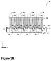
In lieu of, or in combination with the aperture array 130 and baffle structure 160, some embodiments could include a set of vertical, optically-transparent pillars (e.g., optical waveguides) that may serve as a lightguide and couple light to the SiPM devices using total internal reflection. FIG. 2B illustrates a cross-sectional view of an optical system 220, according to an example embodiment. As illustrated in FIG. 2B, optical system 220 could include optical waveguides 222 a, 222 b, 222 c, and 222 d, which could be configured to guide light toward the respective SiPM devices 120 a, 120 b, 120 c, and 120 d. As illustrated, the optical waveguides 222 a, 222 b, 222 c, and 222 d could have a tapered shape. In other examples, the optical waveguides 222 a, 222 b, 222 c, and 222 d could have a straight sidewall and/or take on another shape. In some scenarios, an “active isolation region” could be defined by growing dielectric stacks 224 a, 224 b, 224 c, and 224 d over the respective SiPM devices 120 a, 120 b, 120 c, and 120 d. The dielectric stacks 224 a, 224 b, 224 c, and 224 d could be configured to couple light from the optical waveguides 222 a, 222 b, 222 c, and 222 d into the respective SiPM devices 120 a, 120 b, 120 c, and 120 d. In some embodiments, further optical isolation between SiPM devices 120 a, 120 b, 120 c, and 120 d could be achieved by etching the dielectric stack between SiPM devices and then filling the trenches with an organosiloxane-based planarizing material 226 (e.g., Silecs XC400L or the like). In some embodiments, the planarizing material 226 could have a high refractive index relative to the optical waveguides 222 a, 222 b, 222 c, and 222 d and/or the dielectric stacks 224 a, 224 b, 224 c, and 224 d.
FIG. 2C illustrates a top view 250 of the optical system 200, according to an example embodiment. As illustrated in FIG. 2C, a plurality of SiPM devices 120 could be arranged in a hexagonal array along a surface of a substrate 110. Furthermore, the SiPM devices of the plurality of SiPM devices 120 could be electrically and/or optically isolated from one another by way of one or more isolation trenches 116. In some embodiments, the isolation trenches 116 could be filled with a fill material, as described herein.
It will be understood that various ways could be utilized to electrically and/or optically isolate SiPM devices from one another. For example, while FIG. 2C illustrates a regular hexagonal array, variable spacing and/or variable isolation depths could be utilized between respective receiver channels. For example, in reference to FIG. 2A, receiver channels 140 a, 140 b, 140 c, and 140 d could be isolated by trenches have a first depth (e.g., 1 micron) between some receiver channels and a second depth (e.g., 2 microns) between others. Furthermore, some receiver channels could be spaced further apart from some adjacent receiver channels than for others.
III. Example Methods
FIGS. 3A-3D illustrate various steps of a method of manufacture, according to one or more example embodiments. It will be understood that at least some of the various steps may be carried out in a different order than of that presented herein. Furthermore, steps may be added, subtracted, transposed, and/or repeated. FIGS. 3A-3D may serve as example illustrations for at least some of the steps or blocks described in relation to method 400 as illustrated and described in relation to FIG. 4. Additionally, some steps of FIGS. 3A-3D may be carried out so as to provide optical system 100 and/or optical systems 200 or 220, as illustrated and described in reference to FIGS. 1, 2A, and 2B, respectively.
FIG. 3A illustrates a step of a method of manufacture 300, according to an example embodiment. Step 300 initially includes providing a substrate 110. The substrate 110 may include a first surface 112 and a second surface 114. The substrate 110 could include a semiconductor material, such as a silicon or silicon-on-insulator substrate.
Step 300 could subsequently include forming a plurality of SiPMs 120 a, 120 b, 120 c, and 120 d. In some embodiments, forming the plurality of SiPMs 120 a, 120 b, 120 c, and 120 d could include forming p-n junctions in the first surface 112. That is, the SiPMs 120 a, 120 b, 120 c, and 120 d could be monolithically integrated with the substrate 110. Each SiPM includes a plurality of single photon avalanche diodes (SPADs). In some embodiments, the plurality of SiPMs in the monolithic SiPM array could be arranged in a hexagonal or square array. In such scenarios, the plurality of SiPMs in the monolithic SiPM array could be arranged with a density of about 0.4 SiPMs per mm2.
Step 300 could additionally include forming a plurality of isolation trenches 116 in the first surface 112 of the substrate 110. In some embodiments, forming the plurality of isolation trenches 116 could include etching into the first surface 112 with a wet or dry etch process. Additionally or alternatively, the isolation trenches 116 could be formed by grinding, polishing, or another mechanical method. In some embodiments, the isolation trenches 116 could be arranged between neighboring SiPMs.
Step 300 could further include filling at least a portion of the isolation trenches 116 with a fill material 118. The isolation trenches 116 could be at least partially filled with at least one of: a metal material, an optically-opaque material, a conductive material, or a non-conductive material. As an example, the fill material 118 could be deposited using a chemical vapor deposition process or an oxidation process. The at least one isolation trench could provide electrical isolation between the neighboring SiPMs. Additionally or alternatively, the at least one isolation trench could provide optical isolation between the neighboring SiPMs.
FIG. 3B illustrates a step of a method of manufacture 310, according to an example embodiment. Step 310 includes forming one or more electrical conductors 150 on a first surface 112 and/or a second surface 114 of the substrate 110. The electrical conductors 150 could provide electrical coupling between the SiPMs 120 a, 120 b, 120 c, and 120 d and respective detection circuitry.
FIG. 3C illustrates a step of a method of manufacture 320, according to an example embodiment. Step 320 includes positioning a baffle structure 160 comprising a plurality of openings 162 a, 162 b, 162 c, and 162 d in an optically opaque material. The baffle structure 160 could be positioned so as to align a plurality of diamond-shaped structures with a plurality of isolation trenches 116 and/or the respective SiPMs 120 a, 120 b, 120 c, and 120 d.
In some embodiments, the baffle structure 160 could be positioned between the monolithic SiPM array 120 a, 120 b, 120 c, and 120 d and the aperture array 130, as described herein. In some embodiments, the baffle structure 160 could be positioned with a pick-and-place tool and could be aligned to underlying structures based on registration marks located along the first surface 112.
FIG. 3D illustrates a step of a method of manufacture 330, according to an example embodiment. Step 330 includes aligning an aperture array 130 with respect to the baffle structure 160 and/or the SiPMs 120 a, 120 b, 120 c, and 120 d so as to define a plurality of receiver channels (e.g., receiver channels 140 a, 140 b, 140 c, and 140 d as illustrated and described in reference to FIG. 2A). The aperture array 130 includes a plurality of apertures 132 a, 132 b, 132 c, and 132 d. Each receiver channel includes a respective SiPM of the plurality of SiPMs optically coupled to a respective aperture of the plurality of apertures and a respective opening in the baffle structure.
FIG. 4 illustrates a method 400, according to an example embodiment. Method 400 may be carried out, at least in part, by way of some or all of the manufacturing steps or stages illustrated and described in reference to FIGS. 3A-3D. It will be understood that the method 400 may include fewer or more steps or blocks than those expressly disclosed herein. Furthermore, respective steps or blocks of method 400 may be performed in any order and each step or block may be performed one or more times. In some embodiments, method 400 and its steps or blocks may be performed to provide an optical system that could be similar or identical to optical system 100 and/or optical system 200, as illustrated and described in reference to FIGS. 1 and 2.
Block 402 includes providing a monolithic SiPM array that includes a plurality of silicon photomultipliers (SiPMs) monolithically integrated with a substrate. Each SiPM includes a plurality of single photon avalanche diodes (SPADs). In some embodiments, the plurality of SiPMs in the monolithic SiPM array could be arranged in a hexagonal or square array. In such scenarios, the plurality of SiPMs in the monolithic SiPM array could be arranged with a density of about 0.4 SiPMs per mm2.
In some embodiments, the monolithic SiPM array further includes at least one isolation trench in the substrate, wherein the at least one isolation trench is arranged between neighboring SiPMs. Additionally or alternatively, the at least one isolation trench could be at least partially filled with at least one of: a metal material, an optically-opaque material, a conductive material, or a non-conductive material.
In some examples, the at least one isolation trench could provide electrical isolation between the neighboring SiPMs. Additionally or alternatively, the at least one isolation trench could provide optical isolation between the neighboring SiPMs.
Block 404 includes aligning an aperture array having a plurality of apertures with the monolithic SiPM array so as to define a plurality of receiver channels. Each receiver channel includes a respective SiPM of the plurality of SiPMs optically coupled to a respective aperture of the plurality of apertures.
In some embodiments, method 400 could further include positioning a baffle structure between the monolithic SiPM array and the aperture array. In some scenarios, the baffle structure could include a plurality of openings in an optically opaque material. Positioning the baffle structure could be performed such that each receiver channel is associated with a respective SiPM of the plurality of SiPMs being optically coupled to a respective aperture of the plurality of apertures via a respective opening in the baffle structure.
The particular arrangements shown in the Figures should not be viewed as limiting. It should be understood that other embodiments may include more or less of each element shown in a given Figure. Further, some of the illustrated elements may be combined or omitted. Yet further, an illustrative embodiment may include elements that are not illustrated in the Figures.
A step or block that represents a processing of information can correspond to circuitry that can be configured to perform the specific logical functions of a herein-described method or technique. Alternatively or additionally, a step or block that represents a processing of information can correspond to a module, a segment, a physical computer (e.g., a field programmable gate array (FPGA) or application-specific integrated circuit (ASIC)), or a portion of program code (including related data). The program code can include one or more instructions executable by a processor for implementing specific logical functions or actions in the method or technique. The program code and/or related data can be stored on any type of computer readable medium such as a storage device including a disk, hard drive, or other storage medium.
The computer readable medium can also include non-transitory computer readable media such as computer-readable media that store data for short periods of time like register memory, processor cache, and random access memory (RAM). The computer readable media can also include non-transitory computer readable media that store program code and/or data for longer periods of time. Thus, the computer readable media may include secondary or persistent long term storage, like read only memory (ROM), optical or magnetic disks, compact-disc read only memory (CD-ROM), for example. The computer readable media can also be any other volatile or non-volatile storage systems. A computer readable medium can be considered a computer readable storage medium, for example, or a tangible storage device.
While various examples and embodiments have been disclosed, other examples and embodiments will be apparent to those skilled in the art. The various disclosed examples and embodiments are for purposes of illustration and are not intended to be limiting, with the true scope being indicated by the following claims.

Claims (18)

What is claimed is:
1. An optical system comprising:
a substrate;
a plurality of silicon photomultipliers (SiPMs) monolithically integrated with the substrate, wherein each SiPM comprises a plurality of single photon avalanche diodes (SPADs);
an aperture array comprising a plurality of apertures, wherein the plurality of SiPMs and the aperture array are aligned so as to define a plurality of receiver channels, wherein each receiver channel comprises a respective SiPM of the plurality of SiPMs optically coupled to a respective aperture of the plurality of apertures; and
a baffle structure, wherein the baffle structure comprises a plurality of openings in an optically opaque material, wherein the baffle structure is arranged between the aperture array and the plurality of SiPMs such that each receiver channel comprises a respective SiPM of the plurality of SiPMs optically coupled to a respective aperture of the plurality of apertures via a respective opening in the baffle structure.
2. The optical system of claim 1, wherein the substrate comprises a silicon wafer, an indium phosphide wafer, or a gallium arsenide wafer.
3. The optical system of claim 1, wherein each SiPM of the plurality of SiPMs comprises at least 1000 SPADs.
4. The optical system of claim 1, wherein the plurality of SiPMs are arranged along the substrate in a hexagonal or square array.
5. The optical system of claim 1, wherein the plurality of SiPMs are arranged along the substrate with a density of about 0.4 SiPMs per mm2.
6. The optical system of claim 1, further comprising a plurality of electrical conductors, wherein the plurality of electrical conductors is coupled to the plurality of SiPMs via at least one of: a through substrate via (TSV) or a side routing arrangement.
7. The optical system of claim 1, further comprising at least one isolation trench in the substrate, wherein the at least one isolation trench is arranged between neighboring SiPMs.
8. The optical system of claim 7, wherein the at least one isolation trench is at least partially filled with at least one of: a metal material, an optically-opaque material, a conductive material, or a non-conductive material.
9. The optical system of claim 7, wherein the at least one isolation trench provides electrical isolation or optical isolation between the neighboring SiPMs.
10. The optical system of claim 1, further comprising a plurality of optical waveguides, wherein each optical waveguide is configured to couple light into a respective SiPM of the plurality of SiPMs.
11. The optical system of claim 1, wherein a cross-section of the baffle structure comprises a plurality of diamond-shaped members separated by the respective openings in the baffle structure.
12. A method of manufacturing an optical system, the method comprising:
providing a monolithic SiPM array comprising a plurality of silicon photomultipliers (SiPMs) monolithically integrated with a substrate, wherein each SiPM comprises a plurality of single photon avalanche diodes (SPADs);
aligning an aperture array comprising a plurality of apertures with the monolithic SiPM array so as to define a plurality of receiver channels, wherein each receiver channel comprises a respective SiPM of the plurality of SiPMs optically coupled to a respective aperture of the plurality of apertures; and
positioning a baffle structure comprising a plurality of openings in an optically opaque material between the monolithic SiPM array and the aperture array such that each receiver channel comprises a respective SiPM of the plurality of SiPMs optically coupled to a respective aperture of the plurality of apertures via a respective opening in the baffle structure.
13. The method of claim 12, wherein the plurality of SiPMs in the monolithic SiPM array are arranged in a hexagonal or square array.
14. The method of claim 12, wherein the plurality of SiPMs in the monolithic SiPM array are arranged with a density of about 0.4 SiPMs per mm2.
15. The method of claim 12, wherein the monolithic SiPM array further comprises at least one isolation trench in the substrate, wherein the at least one isolation trench is arranged between neighboring SiPMs.
16. The method of claim 15, wherein the at least one isolation trench is at least partially filled with at least one of: a metal material, an optically-opaque material, a conductive material, or a non-conductive material.
17. The method of claim 15, wherein the at least one isolation trench provides electrical isolation between the neighboring SiPMs.
18. The method of claim 15, wherein the at least one isolation trench provides optical isolation between the neighboring SiPMs.
US16/577,035 2019-09-20 2019-09-20 Monolithic silicon photomultiplier array Active 2039-12-10 US11145778B2 (en)

Priority Applications (7)

Application Number Priority Date Filing Date Title
US16/577,035 US11145778B2 (en) 2019-09-20 2019-09-20 Monolithic silicon photomultiplier array
CN202080065868.3A CN114424347A (en) 2019-09-20 2020-09-18 Monolithic silicon photomultiplier array
JP2022516377A JP7420927B2 (en) 2019-09-20 2020-09-18 Monolithic silicon photomultiplier tube array
PCT/US2020/051370 WO2021055663A1 (en) 2019-09-20 2020-09-18 Monolithic silicon photomultiplier array
EP20866546.3A EP4014253A4 (en) 2019-09-20 2020-09-18 Monolithic silicon photomultiplier array
US17/475,010 US20220052217A1 (en) 2019-09-20 2021-09-14 Monolithic Silicon Photomultiplier Array
IL291442A IL291442A (en) 2019-09-20 2022-03-16 Monolithic silicon photomultiplier array

Applications Claiming Priority (1)

Application Number Priority Date Filing Date Title
US16/577,035 US11145778B2 (en) 2019-09-20 2019-09-20 Monolithic silicon photomultiplier array

Related Child Applications (1)

Application Number Title Priority Date Filing Date
US17/475,010 Continuation US20220052217A1 (en) 2019-09-20 2021-09-14 Monolithic Silicon Photomultiplier Array

Publications (2)

Publication Number Publication Date
US20210091251A1 US20210091251A1 (en) 2021-03-25
US11145778B2 true US11145778B2 (en) 2021-10-12

Family

ID=74881244

Family Applications (2)

Application Number Title Priority Date Filing Date
US16/577,035 Active 2039-12-10 US11145778B2 (en) 2019-09-20 2019-09-20 Monolithic silicon photomultiplier array
US17/475,010 Pending US20220052217A1 (en) 2019-09-20 2021-09-14 Monolithic Silicon Photomultiplier Array

Family Applications After (1)

Application Number Title Priority Date Filing Date
US17/475,010 Pending US20220052217A1 (en) 2019-09-20 2021-09-14 Monolithic Silicon Photomultiplier Array

Country Status (6)

Country Link
US (2) US11145778B2 (en)
EP (1) EP4014253A4 (en)
JP (1) JP7420927B2 (en)
CN (1) CN114424347A (en)
IL (1) IL291442A (en)
WO (1) WO2021055663A1 (en)

Families Citing this family (4)

* Cited by examiner, † Cited by third party
Publication number Priority date Publication date Assignee Title
US11177397B2 (en) * 2020-01-09 2021-11-16 Vanguard International Semiconductor Corporation Semiconductor devices and methods for forming the same
US11729790B2 (en) 2020-08-06 2023-08-15 Samsung Electronics Co., Ltd. Mobile communications methods for monitoring and scheduling
US11870000B2 (en) * 2020-11-17 2024-01-09 Semiconductor Components Industries, Llc Semiconductor packages with single-photon avalanche diodes and prisms
CN115372950B (en) * 2022-10-24 2023-01-20 北醒(北京)光子科技有限公司 Silicon photomultiplier calibration device

Citations (10)

* Cited by examiner, † Cited by third party
Publication number Priority date Publication date Assignee Title
US20090184384A1 (en) 2008-01-18 2009-07-23 Stmicroelectronics S.R.L. Array of mutually isolated, geiger-mode, avalanche photodiodes and manufacturing method thereof
US20110248175A1 (en) * 2008-12-15 2011-10-13 Koninklijke Philips Electronics N.V. Temperature compensation circuit for silicon photomultipliers and other single photon counters
US20120112083A1 (en) * 2010-11-10 2012-05-10 Siemens Aktiengesellschaft High Density, Proportional-Mode, APD Arrays for Individual Scintillator Readout in PET Applications
WO2012168218A2 (en) 2011-06-07 2012-12-13 Siemens Aktiengesellschaft Radiation detector and imaging system
US8975607B2 (en) 2011-04-01 2015-03-10 Stmicroelectronics S.R.L. Confocal optical detector, detector array, and manufacturing method thereof
US9178100B2 (en) 2010-09-08 2015-11-03 Stmicroelectronics (Research & Development) Limited Single photon avalanche diode for CMOS circuits
US20170031010A1 (en) * 2015-07-28 2017-02-02 Kabushiki Kaisha Toshiba Photodetector and lidar system including the photodetector
US9831283B2 (en) 2011-10-31 2017-11-28 The Trustees Of Columbia University In The City Of New York Systems and methods for imaging using single photon avalanche diodes
US20190072649A1 (en) 2017-09-05 2019-03-07 Waymo Llc LIDAR with Co-Aligned Transmit and Receive Paths
US10283541B2 (en) 2014-11-19 2019-05-07 Ams Ag Semiconductor device comprising an aperture array and method of producing such a semiconductor device

Family Cites Families (7)

* Cited by examiner, † Cited by third party
Publication number Priority date Publication date Assignee Title
US8476571B2 (en) * 2009-12-22 2013-07-02 Siemens Aktiengesellschaft SiPM photosensor with early signal digitization
WO2012119094A2 (en) 2011-03-03 2012-09-07 California Institute Of Technology Light guided pixel
JP6612056B2 (en) 2014-05-16 2019-11-27 株式会社半導体エネルギー研究所 Imaging device and monitoring device
KR102657365B1 (en) 2017-05-15 2024-04-17 아우스터, 인크. Brightness Enhanced Optical Imaging Transmitter
US10698088B2 (en) * 2017-08-01 2020-06-30 Waymo Llc LIDAR receiver using a waveguide and an aperture
US10838043B2 (en) 2017-11-15 2020-11-17 Veoneer Us, Inc. Scanning LiDAR system and method with spatial filtering for reduction of ambient light
US11508768B2 (en) 2018-01-11 2022-11-22 Sony Semiconductor Solutions Corporation Solid-state imaging device and electronic apparatus

Patent Citations (10)

* Cited by examiner, † Cited by third party
Publication number Priority date Publication date Assignee Title
US20090184384A1 (en) 2008-01-18 2009-07-23 Stmicroelectronics S.R.L. Array of mutually isolated, geiger-mode, avalanche photodiodes and manufacturing method thereof
US20110248175A1 (en) * 2008-12-15 2011-10-13 Koninklijke Philips Electronics N.V. Temperature compensation circuit for silicon photomultipliers and other single photon counters
US9178100B2 (en) 2010-09-08 2015-11-03 Stmicroelectronics (Research & Development) Limited Single photon avalanche diode for CMOS circuits
US20120112083A1 (en) * 2010-11-10 2012-05-10 Siemens Aktiengesellschaft High Density, Proportional-Mode, APD Arrays for Individual Scintillator Readout in PET Applications
US8975607B2 (en) 2011-04-01 2015-03-10 Stmicroelectronics S.R.L. Confocal optical detector, detector array, and manufacturing method thereof
WO2012168218A2 (en) 2011-06-07 2012-12-13 Siemens Aktiengesellschaft Radiation detector and imaging system
US9831283B2 (en) 2011-10-31 2017-11-28 The Trustees Of Columbia University In The City Of New York Systems and methods for imaging using single photon avalanche diodes
US10283541B2 (en) 2014-11-19 2019-05-07 Ams Ag Semiconductor device comprising an aperture array and method of producing such a semiconductor device
US20170031010A1 (en) * 2015-07-28 2017-02-02 Kabushiki Kaisha Toshiba Photodetector and lidar system including the photodetector
US20190072649A1 (en) 2017-09-05 2019-03-07 Waymo Llc LIDAR with Co-Aligned Transmit and Receive Paths

Non-Patent Citations (1)

* Cited by examiner, † Cited by third party
Title
International Searching Authority, International Search Report and Written Opinion dated Dec. 29, 2020, issued in connection with International Patent Application No. PCT/US2020/051370 filed on Sep. 18, 2020, 10 pages.

Also Published As

Publication number Publication date
WO2021055663A1 (en) 2021-03-25
EP4014253A1 (en) 2022-06-22
EP4014253A4 (en) 2023-08-16
JP2022548093A (en) 2022-11-16
US20220052217A1 (en) 2022-02-17
CN114424347A (en) 2022-04-29
JP7420927B2 (en) 2024-01-23
US20210091251A1 (en) 2021-03-25
IL291442A (en) 2022-05-01

Similar Documents

Publication Publication Date Title
US11145778B2 (en) Monolithic silicon photomultiplier array
US11056525B2 (en) Semiconductor photomultiplier
US10276610B2 (en) Semiconductor photomultiplier
JP7080238B2 (en) Hybrid integration with digital front end of photodetector array
EP3400613B1 (en) Photodiode assembly with an electrostatic discharge guard structure
US20140225216A1 (en) Photodetector
CN112820794A (en) Photodetector, photodetection system, laser radar device, and vehicle
US11735677B2 (en) Photodetectors and photodetector arrays
US20240094358A1 (en) SiPM with Cells of Different Sizes
CN100483751C (en) Semiconductor device
US20230358607A1 (en) Photodetector device
CN213366608U (en) Integrated circuit with a plurality of transistors
CN213988887U (en) Photodetector chip array
KR102283699B1 (en) Single Photon Detector, Avalanche Photodiode for Single Photon Detector and Method for Manufacturing Thereof
US10230008B2 (en) Semiconductor light receiving device, optical receiver module and manufacturing method thereof
JPH0488688A (en) Optical semiconductor integrated device
JPH11135822A (en) Light-receiving circuit

Legal Events

Date Code Title Description
FEPP Fee payment procedure

Free format text: ENTITY STATUS SET TO UNDISCOUNTED (ORIGINAL EVENT CODE: BIG.); ENTITY STATUS OF PATENT OWNER: LARGE ENTITY

AS Assignment

Owner name: WAYMO LLC, CALIFORNIA

Free format text: ASSIGNMENT OF ASSIGNORS INTEREST;ASSIGNORS:ONAL, CANER;DROZ, PIERRE-YVES;DHARIA, NIRAV;REEL/FRAME:050474/0544

Effective date: 20190923

STPP Information on status: patent application and granting procedure in general

Free format text: RESPONSE TO NON-FINAL OFFICE ACTION ENTERED AND FORWARDED TO EXAMINER

STPP Information on status: patent application and granting procedure in general

Free format text: NOTICE OF ALLOWANCE MAILED -- APPLICATION RECEIVED IN OFFICE OF PUBLICATIONS

STPP Information on status: patent application and granting procedure in general

Free format text: PUBLICATIONS -- ISSUE FEE PAYMENT VERIFIED

STCF Information on status: patent grant

Free format text: PATENTED CASE