JP6818875B2 - Laminated back-illuminated SPAD array - Google Patents
Laminated back-illuminated SPAD array Download PDFInfo
- Publication number
- JP6818875B2 JP6818875B2 JP2019511901A JP2019511901A JP6818875B2 JP 6818875 B2 JP6818875 B2 JP 6818875B2 JP 2019511901 A JP2019511901 A JP 2019511901A JP 2019511901 A JP2019511901 A JP 2019511901A JP 6818875 B2 JP6818875 B2 JP 6818875B2
- Authority
- JP
- Japan
- Prior art keywords
- region
- spad
- layer
- anode
- wafer
- Prior art date
- Legal status (The legal status is an assumption and is not a legal conclusion. Google has not performed a legal analysis and makes no representation as to the accuracy of the status listed.)
- Active
Links
- 239000002019 doping agent Substances 0.000 claims description 125
- 239000002800 charge carrier Substances 0.000 claims description 63
- 238000000926 separation method Methods 0.000 claims description 34
- 230000002441 reversible effect Effects 0.000 claims description 29
- 230000015556 catabolic process Effects 0.000 claims description 24
- 239000000463 material Substances 0.000 claims description 24
- 230000003287 optical effect Effects 0.000 claims description 20
- 239000004020 conductor Substances 0.000 claims description 10
- 238000009792 diffusion process Methods 0.000 claims description 10
- 238000002161 passivation Methods 0.000 claims description 6
- 239000011810 insulating material Substances 0.000 claims description 2
- 235000012431 wafers Nutrition 0.000 description 86
- 239000004065 semiconductor Substances 0.000 description 25
- 238000010791 quenching Methods 0.000 description 18
- 230000005684 electric field Effects 0.000 description 14
- VYPSYNLAJGMNEJ-UHFFFAOYSA-N Silicium dioxide Chemical compound O=[Si]=O VYPSYNLAJGMNEJ-UHFFFAOYSA-N 0.000 description 13
- 238000001514 detection method Methods 0.000 description 10
- 229910052710 silicon Inorganic materials 0.000 description 8
- 239000010703 silicon Substances 0.000 description 8
- 230000006870 function Effects 0.000 description 7
- 238000003384 imaging method Methods 0.000 description 7
- 238000000034 method Methods 0.000 description 7
- 229910052814 silicon oxide Inorganic materials 0.000 description 7
- 238000004519 manufacturing process Methods 0.000 description 6
- 230000008569 process Effects 0.000 description 6
- 229910052581 Si3N4 Inorganic materials 0.000 description 4
- 238000004891 communication Methods 0.000 description 4
- 238000010586 diagram Methods 0.000 description 4
- HQVNEWCFYHHQES-UHFFFAOYSA-N silicon nitride Chemical compound N12[Si]34N5[Si]62N3[Si]51N64 HQVNEWCFYHHQES-UHFFFAOYSA-N 0.000 description 4
- 239000000758 substrate Substances 0.000 description 4
- 230000007423 decrease Effects 0.000 description 3
- 230000006698 induction Effects 0.000 description 3
- 238000012986 modification Methods 0.000 description 3
- 230000004048 modification Effects 0.000 description 3
- 229910021420 polycrystalline silicon Inorganic materials 0.000 description 3
- 229920005591 polysilicon Polymers 0.000 description 3
- 230000000171 quenching effect Effects 0.000 description 3
- 230000004044 response Effects 0.000 description 3
- 235000012239 silicon dioxide Nutrition 0.000 description 3
- 239000000377 silicon dioxide Substances 0.000 description 3
- 238000011109 contamination Methods 0.000 description 2
- 238000009826 distribution Methods 0.000 description 2
- 238000005516 engineering process Methods 0.000 description 2
- 238000009413 insulation Methods 0.000 description 2
- 150000002500 ions Chemical class 0.000 description 2
- 238000002955 isolation Methods 0.000 description 2
- 238000005304 joining Methods 0.000 description 2
- 230000007246 mechanism Effects 0.000 description 2
- 229910052751 metal Inorganic materials 0.000 description 2
- 239000002184 metal Substances 0.000 description 2
- 229920001296 polysiloxane Polymers 0.000 description 2
- 229910052594 sapphire Inorganic materials 0.000 description 2
- 239000010980 sapphire Substances 0.000 description 2
- ZOXJGFHDIHLPTG-UHFFFAOYSA-N Boron Chemical compound [B] ZOXJGFHDIHLPTG-UHFFFAOYSA-N 0.000 description 1
- GYHNNYVSQQEPJS-UHFFFAOYSA-N Gallium Chemical compound [Ga] GYHNNYVSQQEPJS-UHFFFAOYSA-N 0.000 description 1
- OAICVXFJPJFONN-UHFFFAOYSA-N Phosphorus Chemical compound [P] OAICVXFJPJFONN-UHFFFAOYSA-N 0.000 description 1
- 230000001154 acute effect Effects 0.000 description 1
- 230000002411 adverse Effects 0.000 description 1
- 229910052787 antimony Inorganic materials 0.000 description 1
- WATWJIUSRGPENY-UHFFFAOYSA-N antimony atom Chemical compound [Sb] WATWJIUSRGPENY-UHFFFAOYSA-N 0.000 description 1
- 230000005540 biological transmission Effects 0.000 description 1
- 230000015572 biosynthetic process Effects 0.000 description 1
- 229910052796 boron Inorganic materials 0.000 description 1
- 238000004364 calculation method Methods 0.000 description 1
- 230000001413 cellular effect Effects 0.000 description 1
- 230000008859 change Effects 0.000 description 1
- 238000006243 chemical reaction Methods 0.000 description 1
- 230000000295 complement effect Effects 0.000 description 1
- 239000000356 contaminant Substances 0.000 description 1
- 239000006059 cover glass Substances 0.000 description 1
- 238000009795 derivation Methods 0.000 description 1
- 230000023077 detection of light stimulus Effects 0.000 description 1
- 238000002059 diagnostic imaging Methods 0.000 description 1
- ALKZAGKDWUSJED-UHFFFAOYSA-N dinuclear copper ion Chemical compound [Cu].[Cu] ALKZAGKDWUSJED-UHFFFAOYSA-N 0.000 description 1
- 229910052733 gallium Inorganic materials 0.000 description 1
- 238000002347 injection Methods 0.000 description 1
- 239000007924 injection Substances 0.000 description 1
- 239000012212 insulator Substances 0.000 description 1
- 229910044991 metal oxide Inorganic materials 0.000 description 1
- 150000004706 metal oxides Chemical class 0.000 description 1
- 150000002739 metals Chemical class 0.000 description 1
- 229910052698 phosphorus Inorganic materials 0.000 description 1
- 239000011574 phosphorus Substances 0.000 description 1
- 230000000630 rising effect Effects 0.000 description 1
- 238000003860 storage Methods 0.000 description 1
- 230000001360 synchronised effect Effects 0.000 description 1
- 230000005469 synchrotron radiation Effects 0.000 description 1
- 230000001960 triggered effect Effects 0.000 description 1
- WFKWXMTUELFFGS-UHFFFAOYSA-N tungsten Chemical compound [W] WFKWXMTUELFFGS-UHFFFAOYSA-N 0.000 description 1
- 229910052721 tungsten Inorganic materials 0.000 description 1
- 239000010937 tungsten Substances 0.000 description 1
Images


Classifications
-
- G—PHYSICS
- G01—MEASURING; TESTING
- G01S—RADIO DIRECTION-FINDING; RADIO NAVIGATION; DETERMINING DISTANCE OR VELOCITY BY USE OF RADIO WAVES; LOCATING OR PRESENCE-DETECTING BY USE OF THE REFLECTION OR RERADIATION OF RADIO WAVES; ANALOGOUS ARRANGEMENTS USING OTHER WAVES
- G01S7/00—Details of systems according to groups G01S13/00, G01S15/00, G01S17/00
- G01S7/48—Details of systems according to groups G01S13/00, G01S15/00, G01S17/00 of systems according to group G01S17/00
- G01S7/483—Details of pulse systems
- G01S7/486—Receivers
- G01S7/4861—Circuits for detection, sampling, integration or read-out
- G01S7/4863—Detector arrays, e.g. charge-transfer gates
-
- H—ELECTRICITY
- H01—ELECTRIC ELEMENTS
- H01L—SEMICONDUCTOR DEVICES NOT COVERED BY CLASS H10
- H01L27/00—Devices consisting of a plurality of semiconductor or other solid-state components formed in or on a common substrate
- H01L27/14—Devices consisting of a plurality of semiconductor or other solid-state components formed in or on a common substrate including semiconductor components sensitive to infrared radiation, light, electromagnetic radiation of shorter wavelength or corpuscular radiation and specially adapted either for the conversion of the energy of such radiation into electrical energy or for the control of electrical energy by such radiation
- H01L27/144—Devices controlled by radiation
- H01L27/146—Imager structures
- H01L27/14601—Structural or functional details thereof
- H01L27/14603—Special geometry or disposition of pixel-elements, address-lines or gate-electrodes
-
- H—ELECTRICITY
- H01—ELECTRIC ELEMENTS
- H01L—SEMICONDUCTOR DEVICES NOT COVERED BY CLASS H10
- H01L27/00—Devices consisting of a plurality of semiconductor or other solid-state components formed in or on a common substrate
- H01L27/14—Devices consisting of a plurality of semiconductor or other solid-state components formed in or on a common substrate including semiconductor components sensitive to infrared radiation, light, electromagnetic radiation of shorter wavelength or corpuscular radiation and specially adapted either for the conversion of the energy of such radiation into electrical energy or for the control of electrical energy by such radiation
- H01L27/144—Devices controlled by radiation
- H01L27/146—Imager structures
- H01L27/14601—Structural or functional details thereof
- H01L27/14609—Pixel-elements with integrated switching, control, storage or amplification elements
- H01L27/1461—Pixel-elements with integrated switching, control, storage or amplification elements characterised by the photosensitive area
-
- H—ELECTRICITY
- H01—ELECTRIC ELEMENTS
- H01L—SEMICONDUCTOR DEVICES NOT COVERED BY CLASS H10
- H01L27/00—Devices consisting of a plurality of semiconductor or other solid-state components formed in or on a common substrate
- H01L27/14—Devices consisting of a plurality of semiconductor or other solid-state components formed in or on a common substrate including semiconductor components sensitive to infrared radiation, light, electromagnetic radiation of shorter wavelength or corpuscular radiation and specially adapted either for the conversion of the energy of such radiation into electrical energy or for the control of electrical energy by such radiation
- H01L27/144—Devices controlled by radiation
- H01L27/146—Imager structures
- H01L27/14601—Structural or functional details thereof
- H01L27/14609—Pixel-elements with integrated switching, control, storage or amplification elements
- H01L27/14612—Pixel-elements with integrated switching, control, storage or amplification elements involving a transistor
- H01L27/14616—Pixel-elements with integrated switching, control, storage or amplification elements involving a transistor characterised by the channel of the transistor, e.g. channel having a doping gradient
-
- H—ELECTRICITY
- H01—ELECTRIC ELEMENTS
- H01L—SEMICONDUCTOR DEVICES NOT COVERED BY CLASS H10
- H01L27/00—Devices consisting of a plurality of semiconductor or other solid-state components formed in or on a common substrate
- H01L27/14—Devices consisting of a plurality of semiconductor or other solid-state components formed in or on a common substrate including semiconductor components sensitive to infrared radiation, light, electromagnetic radiation of shorter wavelength or corpuscular radiation and specially adapted either for the conversion of the energy of such radiation into electrical energy or for the control of electrical energy by such radiation
- H01L27/144—Devices controlled by radiation
- H01L27/146—Imager structures
- H01L27/14601—Structural or functional details thereof
- H01L27/1462—Coatings
- H01L27/14623—Optical shielding
-
- H—ELECTRICITY
- H01—ELECTRIC ELEMENTS
- H01L—SEMICONDUCTOR DEVICES NOT COVERED BY CLASS H10
- H01L27/00—Devices consisting of a plurality of semiconductor or other solid-state components formed in or on a common substrate
- H01L27/14—Devices consisting of a plurality of semiconductor or other solid-state components formed in or on a common substrate including semiconductor components sensitive to infrared radiation, light, electromagnetic radiation of shorter wavelength or corpuscular radiation and specially adapted either for the conversion of the energy of such radiation into electrical energy or for the control of electrical energy by such radiation
- H01L27/144—Devices controlled by radiation
- H01L27/146—Imager structures
- H01L27/14601—Structural or functional details thereof
- H01L27/14625—Optical elements or arrangements associated with the device
- H01L27/14629—Reflectors
-
- H—ELECTRICITY
- H01—ELECTRIC ELEMENTS
- H01L—SEMICONDUCTOR DEVICES NOT COVERED BY CLASS H10
- H01L27/00—Devices consisting of a plurality of semiconductor or other solid-state components formed in or on a common substrate
- H01L27/14—Devices consisting of a plurality of semiconductor or other solid-state components formed in or on a common substrate including semiconductor components sensitive to infrared radiation, light, electromagnetic radiation of shorter wavelength or corpuscular radiation and specially adapted either for the conversion of the energy of such radiation into electrical energy or for the control of electrical energy by such radiation
- H01L27/144—Devices controlled by radiation
- H01L27/146—Imager structures
- H01L27/14601—Structural or functional details thereof
- H01L27/1463—Pixel isolation structures
-
- H—ELECTRICITY
- H01—ELECTRIC ELEMENTS
- H01L—SEMICONDUCTOR DEVICES NOT COVERED BY CLASS H10
- H01L27/00—Devices consisting of a plurality of semiconductor or other solid-state components formed in or on a common substrate
- H01L27/14—Devices consisting of a plurality of semiconductor or other solid-state components formed in or on a common substrate including semiconductor components sensitive to infrared radiation, light, electromagnetic radiation of shorter wavelength or corpuscular radiation and specially adapted either for the conversion of the energy of such radiation into electrical energy or for the control of electrical energy by such radiation
- H01L27/144—Devices controlled by radiation
- H01L27/146—Imager structures
- H01L27/14601—Structural or functional details thereof
- H01L27/14632—Wafer-level processed structures
-
- H—ELECTRICITY
- H01—ELECTRIC ELEMENTS
- H01L—SEMICONDUCTOR DEVICES NOT COVERED BY CLASS H10
- H01L27/00—Devices consisting of a plurality of semiconductor or other solid-state components formed in or on a common substrate
- H01L27/14—Devices consisting of a plurality of semiconductor or other solid-state components formed in or on a common substrate including semiconductor components sensitive to infrared radiation, light, electromagnetic radiation of shorter wavelength or corpuscular radiation and specially adapted either for the conversion of the energy of such radiation into electrical energy or for the control of electrical energy by such radiation
- H01L27/144—Devices controlled by radiation
- H01L27/146—Imager structures
- H01L27/14601—Structural or functional details thereof
- H01L27/14634—Assemblies, i.e. Hybrid structures
-
- H—ELECTRICITY
- H01—ELECTRIC ELEMENTS
- H01L—SEMICONDUCTOR DEVICES NOT COVERED BY CLASS H10
- H01L27/00—Devices consisting of a plurality of semiconductor or other solid-state components formed in or on a common substrate
- H01L27/14—Devices consisting of a plurality of semiconductor or other solid-state components formed in or on a common substrate including semiconductor components sensitive to infrared radiation, light, electromagnetic radiation of shorter wavelength or corpuscular radiation and specially adapted either for the conversion of the energy of such radiation into electrical energy or for the control of electrical energy by such radiation
- H01L27/144—Devices controlled by radiation
- H01L27/146—Imager structures
- H01L27/14601—Structural or functional details thereof
- H01L27/1464—Back illuminated imager structures
-
- H—ELECTRICITY
- H01—ELECTRIC ELEMENTS
- H01L—SEMICONDUCTOR DEVICES NOT COVERED BY CLASS H10
- H01L27/00—Devices consisting of a plurality of semiconductor or other solid-state components formed in or on a common substrate
- H01L27/14—Devices consisting of a plurality of semiconductor or other solid-state components formed in or on a common substrate including semiconductor components sensitive to infrared radiation, light, electromagnetic radiation of shorter wavelength or corpuscular radiation and specially adapted either for the conversion of the energy of such radiation into electrical energy or for the control of electrical energy by such radiation
- H01L27/144—Devices controlled by radiation
- H01L27/146—Imager structures
- H01L27/14643—Photodiode arrays; MOS imagers
-
- H—ELECTRICITY
- H01—ELECTRIC ELEMENTS
- H01L—SEMICONDUCTOR DEVICES NOT COVERED BY CLASS H10
- H01L27/00—Devices consisting of a plurality of semiconductor or other solid-state components formed in or on a common substrate
- H01L27/14—Devices consisting of a plurality of semiconductor or other solid-state components formed in or on a common substrate including semiconductor components sensitive to infrared radiation, light, electromagnetic radiation of shorter wavelength or corpuscular radiation and specially adapted either for the conversion of the energy of such radiation into electrical energy or for the control of electrical energy by such radiation
- H01L27/144—Devices controlled by radiation
- H01L27/146—Imager structures
- H01L27/14665—Imagers using a photoconductor layer
-
- H—ELECTRICITY
- H01—ELECTRIC ELEMENTS
- H01L—SEMICONDUCTOR DEVICES NOT COVERED BY CLASS H10
- H01L31/00—Semiconductor devices sensitive to infrared radiation, light, electromagnetic radiation of shorter wavelength or corpuscular radiation and specially adapted either for the conversion of the energy of such radiation into electrical energy or for the control of electrical energy by such radiation; Processes or apparatus specially adapted for the manufacture or treatment thereof or of parts thereof; Details thereof
- H01L31/08—Semiconductor devices sensitive to infrared radiation, light, electromagnetic radiation of shorter wavelength or corpuscular radiation and specially adapted either for the conversion of the energy of such radiation into electrical energy or for the control of electrical energy by such radiation; Processes or apparatus specially adapted for the manufacture or treatment thereof or of parts thereof; Details thereof in which radiation controls flow of current through the device, e.g. photoresistors
- H01L31/10—Semiconductor devices sensitive to infrared radiation, light, electromagnetic radiation of shorter wavelength or corpuscular radiation and specially adapted either for the conversion of the energy of such radiation into electrical energy or for the control of electrical energy by such radiation; Processes or apparatus specially adapted for the manufacture or treatment thereof or of parts thereof; Details thereof in which radiation controls flow of current through the device, e.g. photoresistors characterised by potential barriers, e.g. phototransistors
- H01L31/101—Devices sensitive to infrared, visible or ultraviolet radiation
- H01L31/102—Devices sensitive to infrared, visible or ultraviolet radiation characterised by only one potential barrier
- H01L31/107—Devices sensitive to infrared, visible or ultraviolet radiation characterised by only one potential barrier the potential barrier working in avalanche mode, e.g. avalanche photodiodes
-
- H—ELECTRICITY
- H04—ELECTRIC COMMUNICATION TECHNIQUE
- H04N—PICTORIAL COMMUNICATION, e.g. TELEVISION
- H04N25/00—Circuitry of solid-state image sensors [SSIS]; Control thereof
- H04N25/50—Control of the SSIS exposure
- H04N25/57—Control of the dynamic range
- H04N25/58—Control of the dynamic range involving two or more exposures
- H04N25/587—Control of the dynamic range involving two or more exposures acquired sequentially, e.g. using the combination of odd and even image fields
-
- H—ELECTRICITY
- H04—ELECTRIC COMMUNICATION TECHNIQUE
- H04N—PICTORIAL COMMUNICATION, e.g. TELEVISION
- H04N25/00—Circuitry of solid-state image sensors [SSIS]; Control thereof
- H04N25/60—Noise processing, e.g. detecting, correcting, reducing or removing noise
- H04N25/617—Noise processing, e.g. detecting, correcting, reducing or removing noise for reducing electromagnetic interference, e.g. clocking noise
-
- H—ELECTRICITY
- H04—ELECTRIC COMMUNICATION TECHNIQUE
- H04N—PICTORIAL COMMUNICATION, e.g. TELEVISION
- H04N25/00—Circuitry of solid-state image sensors [SSIS]; Control thereof
- H04N25/70—SSIS architectures; Circuits associated therewith
- H04N25/709—Circuitry for control of the power supply
-
- H—ELECTRICITY
- H04—ELECTRIC COMMUNICATION TECHNIQUE
- H04N—PICTORIAL COMMUNICATION, e.g. TELEVISION
- H04N25/00—Circuitry of solid-state image sensors [SSIS]; Control thereof
- H04N25/70—SSIS architectures; Circuits associated therewith
- H04N25/71—Charge-coupled device [CCD] sensors; Charge-transfer registers specially adapted for CCD sensors
- H04N25/745—Circuitry for generating timing or clock signals
-
- H—ELECTRICITY
- H04—ELECTRIC COMMUNICATION TECHNIQUE
- H04N—PICTORIAL COMMUNICATION, e.g. TELEVISION
- H04N25/00—Circuitry of solid-state image sensors [SSIS]; Control thereof
- H04N25/70—SSIS architectures; Circuits associated therewith
- H04N25/71—Charge-coupled device [CCD] sensors; Charge-transfer registers specially adapted for CCD sensors
- H04N25/75—Circuitry for providing, modifying or processing image signals from the pixel array
-
- H—ELECTRICITY
- H04—ELECTRIC COMMUNICATION TECHNIQUE
- H04N—PICTORIAL COMMUNICATION, e.g. TELEVISION
- H04N25/00—Circuitry of solid-state image sensors [SSIS]; Control thereof
- H04N25/70—SSIS architectures; Circuits associated therewith
- H04N25/76—Addressed sensors, e.g. MOS or CMOS sensors
- H04N25/77—Pixel circuitry, e.g. memories, A/D converters, pixel amplifiers, shared circuits or shared components
- H04N25/771—Pixel circuitry, e.g. memories, A/D converters, pixel amplifiers, shared circuits or shared components comprising storage means other than floating diffusion
-
- G—PHYSICS
- G01—MEASURING; TESTING
- G01S—RADIO DIRECTION-FINDING; RADIO NAVIGATION; DETERMINING DISTANCE OR VELOCITY BY USE OF RADIO WAVES; LOCATING OR PRESENCE-DETECTING BY USE OF THE REFLECTION OR RERADIATION OF RADIO WAVES; ANALOGOUS ARRANGEMENTS USING OTHER WAVES
- G01S7/00—Details of systems according to groups G01S13/00, G01S15/00, G01S17/00
- G01S7/48—Details of systems according to groups G01S13/00, G01S15/00, G01S17/00 of systems according to group G01S17/00
- G01S7/483—Details of pulse systems
- G01S7/486—Receivers
- G01S7/4861—Circuits for detection, sampling, integration or read-out
-
- H—ELECTRICITY
- H01—ELECTRIC ELEMENTS
- H01L—SEMICONDUCTOR DEVICES NOT COVERED BY CLASS H10
- H01L27/00—Devices consisting of a plurality of semiconductor or other solid-state components formed in or on a common substrate
- H01L27/14—Devices consisting of a plurality of semiconductor or other solid-state components formed in or on a common substrate including semiconductor components sensitive to infrared radiation, light, electromagnetic radiation of shorter wavelength or corpuscular radiation and specially adapted either for the conversion of the energy of such radiation into electrical energy or for the control of electrical energy by such radiation
- H01L27/144—Devices controlled by radiation
- H01L27/146—Imager structures
- H01L27/14601—Structural or functional details thereof
- H01L27/14625—Optical elements or arrangements associated with the device
- H01L27/14627—Microlenses
-
- H—ELECTRICITY
- H01—ELECTRIC ELEMENTS
- H01L—SEMICONDUCTOR DEVICES NOT COVERED BY CLASS H10
- H01L31/00—Semiconductor devices sensitive to infrared radiation, light, electromagnetic radiation of shorter wavelength or corpuscular radiation and specially adapted either for the conversion of the energy of such radiation into electrical energy or for the control of electrical energy by such radiation; Processes or apparatus specially adapted for the manufacture or treatment thereof or of parts thereof; Details thereof
- H01L31/02—Details
- H01L31/02016—Circuit arrangements of general character for the devices
- H01L31/02019—Circuit arrangements of general character for the devices for devices characterised by at least one potential jump barrier or surface barrier
- H01L31/02027—Circuit arrangements of general character for the devices for devices characterised by at least one potential jump barrier or surface barrier for devices working in avalanche mode
-
- H—ELECTRICITY
- H01—ELECTRIC ELEMENTS
- H01L—SEMICONDUCTOR DEVICES NOT COVERED BY CLASS H10
- H01L31/00—Semiconductor devices sensitive to infrared radiation, light, electromagnetic radiation of shorter wavelength or corpuscular radiation and specially adapted either for the conversion of the energy of such radiation into electrical energy or for the control of electrical energy by such radiation; Processes or apparatus specially adapted for the manufacture or treatment thereof or of parts thereof; Details thereof
- H01L31/0248—Semiconductor devices sensitive to infrared radiation, light, electromagnetic radiation of shorter wavelength or corpuscular radiation and specially adapted either for the conversion of the energy of such radiation into electrical energy or for the control of electrical energy by such radiation; Processes or apparatus specially adapted for the manufacture or treatment thereof or of parts thereof; Details thereof characterised by their semiconductor bodies
- H01L31/0352—Semiconductor devices sensitive to infrared radiation, light, electromagnetic radiation of shorter wavelength or corpuscular radiation and specially adapted either for the conversion of the energy of such radiation into electrical energy or for the control of electrical energy by such radiation; Processes or apparatus specially adapted for the manufacture or treatment thereof or of parts thereof; Details thereof characterised by their semiconductor bodies characterised by their shape or by the shapes, relative sizes or disposition of the semiconductor regions
- H01L31/035272—Semiconductor devices sensitive to infrared radiation, light, electromagnetic radiation of shorter wavelength or corpuscular radiation and specially adapted either for the conversion of the energy of such radiation into electrical energy or for the control of electrical energy by such radiation; Processes or apparatus specially adapted for the manufacture or treatment thereof or of parts thereof; Details thereof characterised by their semiconductor bodies characterised by their shape or by the shapes, relative sizes or disposition of the semiconductor regions characterised by at least one potential jump barrier or surface barrier
- H01L31/03529—Shape of the potential jump barrier or surface barrier
Landscapes
- Engineering & Computer Science (AREA)
- Physics & Mathematics (AREA)
- Power Engineering (AREA)
- General Physics & Mathematics (AREA)
- Electromagnetism (AREA)
- Computer Hardware Design (AREA)
- Microelectronics & Electronic Packaging (AREA)
- Condensed Matter Physics & Semiconductors (AREA)
- Signal Processing (AREA)
- Multimedia (AREA)
- Computer Networks & Wireless Communication (AREA)
- Radar, Positioning & Navigation (AREA)
- Remote Sensing (AREA)
- Solid State Image Pick-Up Elements (AREA)
- Light Receiving Elements (AREA)
- Transforming Light Signals Into Electric Signals (AREA)
- Photometry And Measurement Of Optical Pulse Characteristics (AREA)
Description
(関連出願の相互参照)
この特許協力条約特許出願は、2016年9月23日に出願された「Back−Illuminated SPAD Image Sensor」と題する米国仮特許出願第62/398,712号、及び2016年9月23日に出願された「Back−Illuminated SPAD Image Sensor」と題する米国仮特許出願第62/398,709号に対する優先権を主張し、これらの内容は、それらの全体が参照により本明細書に組み込まれている。
(Cross-reference of related applications)
This Patent Cooperation Treaty patent application was filed on September 23, 2016 in US Provisional Patent Application No. 62 / 398,712 entitled "Back-Illuminated SPAD Image Sensor" and on September 23, 2016. It claims priority to US Provisional Patent Application No. 62 / 398,709 entitled "Back-Illuminated SPAD Image Sensor", the contents of which are incorporated herein by reference in their entirety.
記載された実施形態は、一般に、単一光子アバランシェダイオード(SPAD)画像センサに関する。 The embodiments described generally relate to a single photon avalanche diode (SPAD) image sensor.
画像センサは、デジタルカメラ、携帯電話、コピー機、医療撮像デバイス、セキュリティシステム、及び飛行時間型カメラなどの様々な電子デバイスに使用されている。画像センサは典型的に、入射光を検出又はそれに応答する光検出器のアレイを含む。画像センサに使用できる光検出器の1つのタイプは、単一光子アバランシェダイオード(SPAD)領域である。SPAD領域は、(単一光子まで下がった)低レベルの光を検出し、光子の到着時間を知らせるように構成された感光性領域である。 Image sensors are used in a variety of electronic devices such as digital cameras, mobile phones, copiers, medical imaging devices, security systems, and time-of-flight cameras. Image sensors typically include an array of photodetectors that detect or respond to incident light. One type of photodetector that can be used in image sensors is the single photon avalanche diode (SPAD) region. The SPAD region is a photosensitive region configured to detect low levels of light (down to a single photon) and signal the arrival time of the photon.
モノリシック集積SPAD画像センサは典型的に、SPAD領域のアレイ及びSPAD領域用の電気回路を含む。しかしながら、SPAD領域用の電気回路は半導体ウェハ上のスペースを消費するので、アレイのフィルファクタは制限され得る。加えて、モノリシック集積SPAD画像センサの製造中に、半導体ウェハの汚染を防止することは困難であり得る。金属及び他の汚染物質は、SPAD画像センサ内のノイズを増大させるなどによって、SPAD画像センサの性能に悪影響を及ぼす可能性がある。 A monolithic integrated SPAD image sensor typically includes an array in the SPAD region and an electrical circuit for the SPAD region. However, the fill factor of the array can be limited because the electrical circuit for the SPAD region consumes space on the semiconductor wafer. In addition, it can be difficult to prevent contamination of semiconductor wafers during the manufacture of monolithic integrated SPAD image sensors. Metals and other contaminants can adversely affect the performance of the SPAD image sensor, such as by increasing noise in the SPAD image sensor.
いくつかの例では、光子検出効率とSPAD領域のタイミング応答との間にトレードオフがあり得る。より厚い半導体ウェハによってSPAD領域の光子検出効率を改善することができるが、電荷キャリアがより厚い半導体ウェハを通って伝播しなければならないので、より厚い半導体ウェハは、SPAD領域の時間分解能又は応答時間を低下させる可能性がある。加えて、より厚い半導体ウェハはより高いブレークダウン電圧を生じ得るので、SPAD画像センサがガイガーモードで動作している場合、SPAD画像センサの電力消費を増大させる可能性がある。 In some examples, there may be a trade-off between photon detection efficiency and timing response in the SPAD region. Thicker semiconductor wafers can improve photon detection efficiency in the SPAD region, but thicker semiconductor wafers have time resolution or response time in the SPAD region because charge carriers must propagate through the thicker semiconductor wafers. May decrease. In addition, thicker semiconductor wafers can generate higher breakdown voltage, which can increase the power consumption of the SPAD image sensor when operating in Geiger mode.
一態様では、背面照射型単一光子アバランシェダイオード(SPAD)画像センサは、センサウェハ、及びセンサウェハの下に配置され、センサウェハに取り付けられた回路ウェハを含む。センサウェハは、第1のドーパント型を含むアノード領域と、第2のドーパント型を含み、SPAD領域の前面に隣接して配置されたカソード領域と、を含むSPAD領域を含む。アノード領域は、アノード勾配層、及び第1のドーパント型を含みカソード領域の上方に配置されたアノードアバランシェ層を含む。エッジブレークダウンを減少させるために、カソード領域は第1の面積を有し、アノードアバランシェ層は第1の面積よりも小さい第2の面積を有する。アノード勾配層における第1のドーパント型のドーパント濃度は、アノード勾配層にドーパント濃度勾配を生じさせるため、アノード勾配層の背面でより高く、アノード勾配層の前面でより低い。ドーパント濃度勾配は、アノード勾配層を介して、光子生成電荷キャリアをアノードアバランシェ層まで導くことができる。背面照射型SPADセンサは、SPAD領域に隣接するディープトレンチ分離領域を含んでもよい。 In one aspect, the back-illuminated single photon avalanche diode (SPAD) image sensor includes a sensor wafer and a circuit wafer that is located beneath the sensor wafer and attached to the sensor wafer. The sensor wafer includes an anode region containing a first dopant type and a SPAD region containing a second dopant type and including a cathode region located adjacent to the front surface of the SPAD region. The anode region includes an anode gradient layer and an anode avalanche layer containing a first dopant type and located above the cathode region. To reduce edge breakdown, the cathode region has a first area and the anode avalanche layer has a second area that is smaller than the first area. The dopant concentration of the first dopant type in the anode gradient layer is higher on the back surface of the anode gradient layer and lower on the front surface of the anode gradient layer because it causes a dopant concentration gradient in the anode gradient layer. The dopant concentration gradient can guide photon-producing charge carriers to the anode avalanche layer via the anode gradient layer. The back-illuminated SPAD sensor may include a deep trench separation region adjacent to the SPAD region.
別の態様では、背面照射型単一光子アバランシェダイオード(SPAD)画像センサを含む電子デバイスを開示する。SPAD画像センサは、センサウェハ、及びセンサウェハの前面に取り付けられた回路ウェハを含む。センサウェハは、第1のSPAD領域、及び第1のSPAD領域に隣接する第2のSPAD領域を含む。第1及び第2のSPAD領域はそれぞれ、第1のドーパントを含むアノード勾配層と、アノード勾配層の前面に隣接し、第2のドーパントを含むカソード領域と、カソード領域の上方に配置され、第1のドーパントを含むアノードアバランシェ層と、を含む。センサ層はまた、第1のSPAD領域と第2のSPAD領域との間に配置され、センサウェハの背面から延在するディープトレンチ分離領域を含む。電子デバイスはまた、背面照射型(SPAD)画像センサに動作可能に接続された処理デバイスを含む。処理デバイスは、背面照射型(SPAD)画像センサから出力信号を受信するように構成されていてもよい。 In another aspect, an electronic device comprising a back-illuminated single photon avalanche diode (SPAD) image sensor is disclosed. The SPAD image sensor includes a sensor wafer and a circuit wafer mounted on the front surface of the sensor wafer. The sensor wafer includes a first SPAD region and a second SPAD region adjacent to the first SPAD region. The first and second SPAD regions are located adjacent to the front surface of the anode gradient layer containing the first dopant and the cathode region containing the second dopant, respectively, and are located above the cathode region. Includes an anode avalanche layer containing the dopant of 1. The sensor layer is also located between the first SPAD region and the second SPAD region and includes a deep trench separation region extending from the back surface of the sensor wafer. Electronic devices also include processing devices operably connected to a back-illuminated (SPAD) image sensor. The processing device may be configured to receive an output signal from a back-illuminated (SPAD) image sensor.
更なる実施形態では、ディープトレンチ分離領域は、第1のSPAD領域と第2のSPAD領域との間に配置される。ディープトレンチ分離領域はセンサウェハの背面を通って延在し、光シールドはディープトレンチ分離領域の上方に配置されている。処理デバイスは、背面照射型SPAD画像センサから出力信号を受信し、その出力信号に基づいて飛行時間データを判定するように構成されている。 In a further embodiment, the deep trench separation region is located between the first SPAD region and the second SPAD region. The deep trench isolation region extends through the back of the sensor wafer and the optical shield is located above the deep trench isolation region. The processing device is configured to receive an output signal from the back-illuminated SPAD image sensor and determine flight time data based on the output signal.
更に別の態様では、電子デバイスは、処理デバイスに動作可能に結合された背面照射型単一光子アバランシェダイオード(SPAD)画像センサを含む。SPAD画像センサは、センサウェハ、及びセンサウェハの下に積層された回路ウェハを含む。センサウェハは、ディープトレンチ分離領域によって分離されたSPAD領域のアレイを含む。各SPAD領域は、第1のドーパント型を含むアノード勾配層と、SPAD領域の前面に隣接して配置され、第2のドーパント型を含むカソード領域と、カソード領域の上方に配置され、第1のドーパント型を含むアノードアバランシェ層と、を含む。アノード勾配層内の第1のドーパント型は、アノード勾配層の背面に隣接するドーパント濃度がアノード勾配層の前面に隣接するドーパント濃度と比べてより高いドーパント濃度勾配で構成されている。ドーパント濃度勾配は、光子生成電荷キャリアをアノードアバランシェ層に導く。エッジブレークダウンを減少させるために、カソード領域は第1の面積を有し、アノードアバランシェ層は第1の面積よりも小さい第2の面積を有する。ディープトレンチ分離領域は、SPAD領域のアレイ内の各SPAD領域に隣接しており、光シールドはディープトレンチ分離領域の上方に配置されている。ディープトレンチ分離領域及び光シールドは、SPAD領域間の光学的及び電気的クロストークを低減又は抑制することができる。ディープトレンチ分離領域は、導電材料を含んでもよく、又は交互する低屈折率材料層と高屈折率材料層を含んでもよい。 In yet another aspect, the electronic device includes a back-illuminated single photon avalanche diode (SPAD) image sensor operably coupled to the processing device. The SPAD image sensor includes a sensor wafer and a circuit wafer laminated under the sensor wafer. The sensor wafer contains an array of SPAD regions separated by a deep trench separation region. Each SPAD region is arranged adjacent to the front surface of the anode gradient layer containing the first dopant type, the cathode region containing the second dopant type, and above the cathode region, the first. Includes an anode avalanche layer, including a dopant type. The first dopant type in the anode gradient layer is composed of a dopant concentration gradient in which the dopant concentration adjacent to the back surface of the anode gradient layer is higher than the dopant concentration adjacent to the front surface of the anode gradient layer. The dopant concentration gradient guides the photon-producing charge carriers to the anode avalanche layer. To reduce edge breakdown, the cathode region has a first area and the anode avalanche layer has a second area that is smaller than the first area. The deep trench separation region is adjacent to each SPAD region in the array of SPAD regions, and the optical shield is located above the deep trench separation region. Deep trench separation regions and optical shields can reduce or suppress optical and electrical crosstalk between SPAD regions. The deep trench separation region may include a conductive material, or may include alternating low index material layers and high index material layers.
本開示は、添付の図面と併せて以下の詳細な説明によって容易に理解され、同様の参照番号は同様の構造要素を示す。 The present disclosure is readily understood by the following detailed description in conjunction with the accompanying drawings, with similar reference numbers indicating similar structural elements.
添付の図でのクロスハッチング又はシェーディングの使用は、概して、隣り合う要素間の境界を明らかにし、図の視認性も促進するためにも提供される。したがって、クロスハッチング又はシェーディングの存在も不在も、添付の図に示される任意の要素に関する特定の材料、材料特性、要素の割合、要素の寸法、同様に図示されている要素の共通点、又は任意の他の特質、属性、若しくは特性についてのいかなる選好又は要件も伝達又は指示するものではない。 The use of cross-hatching or shading in the attached figures is also generally provided to reveal boundaries between adjacent elements and also to enhance the visibility of the figure. Thus, with or without cross-hatching or shading, the particular material, material properties, element proportions, element dimensions, commonalities of the elements shown as well, or any of the elements shown in the attached figure. It does not convey or direct any preference or requirement for any other property, attribute, or property.
追加的に、種々の特徴及び要素(並びにそれらの集合及び群)の(相対的であれ絶対的であれ)割合及び寸法、並びにそれらの間に提示される境界、分離点及び位置関係は、単に本明細書に述べられる種々の実施形態の理解を容易にするために添付の図に提供されるものであり、したがって必ずしも一定の縮尺で提示又は図示されていない場合があり、図示される実施形態についての任意の選好又は要件を、それを参照して述べられる実施形態を除外して示す意図はないことを理解されたい。 In addition, the proportions and dimensions (relative or absolute) of various features and elements (and their sets and groups), as well as the boundaries, separation points and positional relationships presented between them, are simply The embodiments provided herein are provided in the accompanying figures to facilitate understanding of the various embodiments described herein, and thus may not necessarily be presented or shown to a certain scale and are shown. It should be understood that there is no intention to indicate any preference or requirement for. Excluding embodiments described with reference to it.
ここで、添付の図面に示された代表的な実施形態を詳細に参照する。以下の説明は、これらの実施形態を1つの好ましい実施形態に限定することを意図するものではないことを理解されたい。反対に、以下の説明は、添付の特許請求の範囲によって定義される記述されている実施形態の趣旨及び範囲に含まれ得る代替形態、修正形態、及び均等物を対象として含むことを意図するものである。 Here, the representative embodiments shown in the accompanying drawings will be referred to in detail. It should be understood that the following description is not intended to limit these embodiments to one preferred embodiment. On the contrary, the following description is intended to cover alternatives, modifications, and equivalents that may be included in the intent and scope of the described embodiments as defined by the appended claims. Is.
以下の開示は、背面照射型単一光子アバランシェダイオード(SPAD)画像センサに関する。SPAD画像センサは、センサウェハ、及びセンサウェハの前面に取り付けられた、又は接合された別個の回路ウェハを含む。センサウェハは1つ以上のSPAD領域を含む。各SPAD領域は、光感知半導体セクションを含み、SPAD画像センサの画素要素として機能する、すなわち、光子を受け取り、電流を生成する。各SPADの半導体セクションはダイオードとして構成されている。SPAD領域は、ダイオードセクションをそのアバランシェ領域に逆バイアスすることによって光を検出することが可能になる。入射する光子は、アバランシェ電流を誘起する電荷キャリアを生成する。回路ウェハは、SPAD領域(単数又は複数)に接続し、アバランシェ電流を検出する電気回路を含む。いくつかの実施形態では、各SPAD領域は、第1のウェハ間コネクタを介して少なくとも1つの電圧源に接続され、第2のウェハ間コネクタを介して出力回路に接続される。 The following disclosure relates to a back-illuminated single photon avalanche diode (SPAD) image sensor. The SPAD image sensor includes a sensor wafer and a separate circuit wafer attached or bonded to the front surface of the sensor wafer. The sensor wafer contains one or more SPAD regions. Each SPAD region includes a light-sensing semiconductor section and functions as a pixel element of the SPAD image sensor, i.e., it receives photons and generates current. The semiconductor section of each SPAD is configured as a diode. The SPAD region makes it possible to detect light by reverse biasing the diode section into its avalanche region. The incident photons generate charge carriers that induce an avalanche current. Circuit wafers include electrical circuits that connect to the SPAD region (s) and detect avalanche currents. In some embodiments, each SPAD region is connected to at least one voltage source via a first interwafer connector and to an output circuit via a second interwafer connector.
センサウェハはSPAD領域を主に含むので、センサウェハの製造プロセスはSPAD領域の製造のために最適化することができる。同様に、回路ウェハの製造プロセスは、回路ウェハ内の電気回路に対して最適化されてもよい。センサウェハには電気回路が含まれていないので、センサウェハの汚染が低減又は除去される。 Since the sensor wafer mainly includes the SPAD region, the manufacturing process of the sensor wafer can be optimized for manufacturing the SPAD region. Similarly, the circuit wafer manufacturing process may be optimized for the electrical circuits within the circuit wafer. Since the sensor wafer does not contain an electrical circuit, contamination of the sensor wafer is reduced or eliminated.
以下でより十分に説明するように、いくつかのSPAD領域は、光を受け入れるように構成された表面(「背面」と呼ぶ)、光子生成電荷キャリア(例えば電子)をアノード勾配層の側縁部からアノード勾配層の内側(すなわち中央)に導くように構成されたアノード勾配層を含む。電荷キャリアは次いで、SPAD領域のアノードアバランシェ層に向かって導かれる。アノードアバランシェ層では、電荷キャリアが更に電荷キャリアを誘起させ、それによってその電荷キャリアがカソード領域において反対型の電荷キャリアと結合する。その結果、SPAD領域に電流パルスが入る。一実施形態では、SPAD領域は、SPAD領域の第1の側縁部(例えば左側縁部)に隣接して配置された第1の側縁部ドーパント濃度勾配、及びSPAD領域の対向する側縁部(例えば右側縁部)に隣接して配置された第2の側縁部ドーパント濃度勾配を含む。別のドーパント濃度勾配は、アノード勾配層内で、低濃度ドープ層からアノード勾配層又はSPAD領域の背面まで垂直方向に増大し得る。 As will be more fully described below, some SPAD regions have surfaces (referred to as "backsides") configured to receive light, photon-producing charge carriers (eg, electrons) at the lateral edges of the anode gradient layer. Includes an anode gradient layer configured to lead from to the inside (ie, center) of the anode gradient layer. Charge carriers are then guided towards the anode avalanche layer in the SPAD region. In the anode avalanche layer, charge carriers further induce charge carriers, thereby binding to opposite charge carriers in the cathode region. As a result, a current pulse enters the SPAD region. In one embodiment, the SPAD region is a first side edge dopant concentration gradient located adjacent to a first side edge of the SPAD region (eg, the left edge), and an opposite side edge of the SPAD region. Includes a second side edge dopant concentration gradient located adjacent (eg, right edge). Another dopant concentration gradient can increase vertically within the anode gradient layer from the low concentration doped layer to the back of the anode gradient layer or the SPAD region.
いくつかの実施形態では、ガードリング層は、各SPAD領域内のアノードアバランシェ層及びカソード領域に隣接して又は隣に配置することができる。ガードリング層は、カソード領域とアノードアバランシェ層との間の最大電界を緩和するように構成されている。アノードアバランシェ層の幅及び長さは、ガードリング層に基づいて拡張されてもよい。 In some embodiments, the guard ring layer can be placed adjacent to or next to the anode avalanche layer and cathode region within each SPAD region. The guard ring layer is configured to relax the maximum electric field between the cathode region and the anode avalanche layer. The width and length of the anode avalanche layer may be extended based on the guard ring layer.
ディープトレンチ分離(DTI)領域は、SPAD領域に隣接してその周囲でセンサウェハ内に配置される。DTI領域は、センサウェハの背面からSPAD領域の前面まで延在して、電気的及び光学的クロストークを低減又は抑制する。いくつかの実施形態では、DTI領域は、センサウェハの背面(受光面)を通って延在する。光学的クロストークを更に低減するために、光シールドをセンサウェハの背面上(例えば、DTI領域上)に配置することができる。 The Deep Trench Separation (DTI) region is located in the sensor wafer adjacent to and around the SPAD region. The DTI region extends from the back surface of the sensor wafer to the front surface of the SPAD region to reduce or suppress electrical and optical crosstalk. In some embodiments, the DTI region extends through the back surface (light receiving surface) of the sensor wafer. To further reduce optical crosstalk, an optical shield can be placed on the back surface of the sensor wafer (eg, on the DTI region).
SPAD領域の半導体セクション容積の側壁を形成するものなど、DTI領域の外面は、ピンニング層及び/又はパッシベーション層を有することができる。いくつかの実施形態では、SPAD領域の前面に隣接するDTI領域の一部上にドープウェルを配置して、SPAD領域への電気的接続を提供することができる。ピンニング層がDTI領域の外面上に配置される場合、ドープウェルはピンニング層に接続することができる。 The outer surface of the DTI region can have a pinning layer and / or a passivation layer, such as one that forms a side wall of the semiconductor section volume of the SPAD region. In some embodiments, a dope well can be placed on a portion of the DTI region adjacent to the anterior surface of the SPAD region to provide electrical connectivity to the SPAD region. If the pinning layer is placed on the outer surface of the DTI region, the dope well can be connected to the pinning layer.
いくつかの実施形態では、逆バイアス電圧源とは別個の絶縁電圧源と、DTI領域に含まれる導電材料との間に、電気的接続が行われる。導電材料に印加される絶縁電圧は、SPAD領域間のクロストークを防止し、光子生成電荷キャリアをアバランシェ領域に向けることができる。接続は、SPAD領域のDTI領域内のビアを介して行うことができる。他のビアは、逆バイアス電圧源との接続を可能にするために、DTI領域の一部であってもよい。DTI領域を介して使用されるビアは、集光専用により大きな領域を可能にすることができる。 In some embodiments, an electrical connection is made between an insulating voltage source separate from the reverse bias voltage source and the conductive material contained in the DTI region. The insulating voltage applied to the conductive material can prevent crosstalk between the SPAD regions and direct the photon generating charge carriers to the avalanche region. The connection can be made via vias within the DTI region of the SPAD region. The other vias may be part of the DTI region to allow connection with a reverse bias voltage source. Vias used through the DTI region can allow a larger region dedicated to focusing.
更に、光リフレクタを各SPAD領域の少なくとも一部の下に配置して、最初に検出されなかった光子をセンサウェハのSPAD領域内に反射し戻して、電荷キャリアの生成を誘起することができる。反射された光子が追加の光子生成電荷キャリアを生成することができるため、光子を反射してSPAD領域に戻すことは、各SPAD領域の光子検出効率(PDE)を増大させることができる。 In addition, an optical reflector can be placed below at least a portion of each SPAD region to reflect the initially undetected photons back into the SPAD region of the sensor wafer to induce the formation of charge carriers. Reflecting photons back into the SPAD region can increase the photon detection efficiency (PDE) of each SPAD region, as the reflected photons can generate additional photon-producing charge carriers.
これら及び他の実施形態について、図1〜図8を参照して以下に論じる。しかしながら、当業者であれば、これらの図に関して本明細書に与えられた発明を実施するための形態は説明の目的のためのものに過ぎず、限定するものとして解釈されるべきではないことを容易に理解するであろう。 These and other embodiments will be discussed below with reference to FIGS. 1-8. However, those skilled in the art will appreciate that the embodiments of the invention given herein with respect to these figures are for illustration purposes only and should not be construed as limiting. It will be easy to understand.
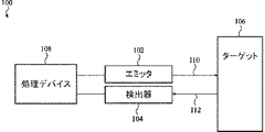
図1は、1つ以上のSPAD画像センサを含むシステムの一例を示す。システム100は、エミッタ102、検出器104、及びターゲット106を含む。エミッタ102及び検出器104のそれぞれは、1つ以上のエミッタ及び検出器をそれぞれ表す。エミッタ102はターゲット106に向けて光を放射するように配置され、検出器104はシーン及び/又はターゲット106から反射された光を検出するように配置されている。
FIG. 1 shows an example of a system including one or more SPAD image sensors.
処理デバイス108は、エミッタ102と検出器104とに動作可能に接続されている。光が検出されると、処理デバイス108は、エミッタ102に、ターゲット106に向けて光を放射させる(矢印110によって表される放射光)。ターゲット106から反射された光は、次いで検出器104によって検出される(矢印112によって表される反射光)。処理デバイス108は、検出器104からの出力信号を受信し、出力信号を処理して反射光、ターゲット106、及び/又はシーンに関連付けられた1つ以上の特性を判定する。
The
図2は、図1に示す検出器の一例の断面図を描写する。検出器200は、SPAD画像センサ204と光学的に通信している撮像段202を含む。撮像段202は、検出器200のエンクロージャ206に動作可能に接続され、SPAD画像センサ204の前に配置されている。撮像段202は、レンズ、フィルタ、絞り、及びシャッタなどの従来の要素を含むことができる。撮像段202は、その視野内の光208を、SPAD画像センサ204上に向け、合焦させ、又は透過させる。SPAD画像センサ204は、入射光子を電気信号に変換することによって光(例えば、図1の反射光112)を検出する。
FIG. 2 depicts a cross-sectional view of an example of the detector shown in FIG. The
SPAD画像センサ204は、支持構造体210を含むか、又は支持構造210によって支持され得る。支持構造体210は、シリコン、シリコンオンインシュレータ(SOI)技術、シリコンオンサファイア(SOS)技術、ドープ半導体及び非ドープ半導体、半導体基板上に形成されたエピタキシャル層、半導体基板中に形成されたウェル領域若しくは埋込み層、並びに他の半導体構造が挙げられるが、これらには限定されない半導体ベースの材料とすることができる。
The
撮像段202又はSPAD画像センサ204の様々な要素は、処理デバイス又はメモリ(例えば、図1の処理デバイス108、図8の処理デバイス804、及び図8のメモリ806)から供給されるタイミング信号又は他の信号によって制御することができる。撮像段202の要素の一部又は全部は、単一の構成要素中に統合してもよい。加えて、撮像段202の要素の一部又は全部を、SPAD画像センサ204と、場合によっては検出器200の1つ以上の追加の要素と統合して、カメラモジュールを形成することができる。例えば、いくつかの実施形態では、プロセッサ又はメモリをSPAD画像センサ204と統合することができる。
The various elements of the imaging stage 202 or the
図3Aは、背面照射型SPAD画像センサの一例の断面図を示す。背面照射型SPAD画像センサ300は、回路ウェハ304上に垂直に積層されたセンサウェハ302を含む。具体的には、回路ウェハ304の背面は、インタフェース306において、センサウェハ302の前面に取り付けられるか、又は接合される。図3Aでは1つの回路ウェハ304のみを描いているが、他の実施形態では複数の回路ウェハを含むことができる。
FIG. 3A shows a cross-sectional view of an example of a back-illuminated SPAD image sensor. The back-illuminated
センサウェハ302及び回路ウェハ304はそれぞれ、任意の好適な材料で形成することができる。一実施形態では、センサウェハ302及び回路ウェハ304は、半導体ベースの材料で形成される。前述のように、例示的な半導体ベースの材料は、シリコン、シリコン−絶縁体−シリコン、サファイア上のシリコン、ドープ及び非ドープ半導体を含む。センサウェハ302及び回路ウェハ304は、半導体基板上に形成されたエピタキシャル層、並びに、半導体基板内に形成された領域又は埋め込み層、及び他の同様の構造として形成することができる。
The
図3Aの例示的実施形態では、センサウェハ302は、SPAD領域308のアレイを含む。各SPAD領域308は、ダイオード構造を実装するためにアノード領域及びカソード領域を含む。アノード領域は、どちらも第1のドーパント型でドープされた、アノードアバランシェ層314及びアノード勾配層310を含む。カソード領域312は、第2のドーパント型でドープされている。いくつかの実施形態では、アノード領域はp型ドープシリコンを含み、カソード領域312はn型ドープシリコンを含む。しかしながら、以下に記載する実施形態では、これらのドーピング型を逆にすること、又は代替の半導体材料を使用することも可能である。カソード領域312は、センサウェハ302と回路ウェハ304との間の境界面306により近いアノード勾配層310の側に配置されている。例えば、カソード領域312は、半導体ベースのアノード勾配層310と二酸化シリコン層315との間の境界面313において、アノード勾配層310の前面に配置されてもよい。カソード領域312は、第1の横幅(図7のW1を参照)及び第1の横方向長さ(図7のL1を参照)を有する。SPAD領域は、実質的に平行な柱として形作られる。背面336及び境界面313などの柱の端面は、正方形、矩形、楕円形又は他の平面形状として形作ることができる。それらの横方向の寸法は、2つの垂直方向における前面及び背面の最大範囲を指し、必ずしも前面又は背面の矩形形状を意味するものではない。背面336及び境界面313からの距離は、SPAD領域の横方向の幅及び長さのいずれより大きくても、小さくても、又は等しくてもよい。
In the exemplary embodiment of FIG. 3A, the
アノード勾配層310は、ダイオード構造のアノード領域の一部を形成し、カソード領域312はダイオード構造のカソードを形成する。アノード領域はまた、カソード領域312上に形成され、こちらも第1のドーパント型でドープされたアノードアバランシェ層314を含む。アノードアバランシェ層314は、第2の横幅及び第2の横方向長さ(図7に示す特定の形状に対してそれぞれW2及びL2)を有する。いくつかの実施形態では、アノードアバランシェ層314の面積(L2×W2)がカソード領域312の面積(L1×W1)よりも小さくなるように、W2はW1よりも小さく、L2はL1よりも小さい。アノードアバランシェ層314の面積がカソード領域312の面積よりも小さい場合、エッジブレークダウンが減少又は回避される。
The
アノードアバランシェ層314は、センサウェハの製造中にアノード勾配層310内に特に生成される領域であってもよい。SPAD領域308に逆バイアスが印加されていない場合、アノードアバランシェ層314は、カソード領域312共に形成されたp−n接合を形成する空乏領域の全部又は一部を包含してもよい。一般に、いかなる逆バイアス電圧も存在しない場合、空乏領域はカソード領域を囲み、一方、アノードアバランシェ層はアノードとカソードとの間の空乏領域の一部である。アノード勾配層310とアノードアバランシェ層314とを合わせてアノード領域と呼ぶこととする。
The
SPAD領域308が光を検出することを有効化されると、アノード領域とカソード領域312との間のp−n接合は、ブレークダウン電圧で又はそれを超える電圧で逆バイアスされる。そのように有効化されると、背面336を通ってアノード勾配層310に入る光の光子は、電子−正孔生成によって光子生成電荷キャリア(例えば、電子)を生成する。光子生成電荷キャリアは、アノード勾配層310の逆バイアス拡大空乏領域(例えば、図4Aの空乏層418を参照)内に注入される。これによって、SPAD領域308の出力における出力信号(例えば、電流)を急速に上昇させる自己持続的アバランシェを引き起こすことができる。電流出力パルスの立ち上がりエッジは、検出された光子の到達時間を示す。バイアス電圧をブレークダウン電圧又はそれを下回る電圧まで低下させることにより、アバランシェがクエンチするまで電流が継続する。いくつかの実施形態では、アバランシェ領域は、ブレークダウン電圧に達する直前に完全に空乏化されてもよい。(以下、「空乏化された」領域又は層は、「完全に空乏化された」ことを意味すると理解されたい)。SPAD領域308は、バイアス電圧がブレークダウン電圧まで、若しくはそれを下回るか、又は特定の実施形態では直下に減少すると、本質的にリセットされる。ある期間後、バイアス電圧はブレークダウン電圧よりも大きいレベルに復帰し、SPAD領域308は別の光子を検出することができる。SPAD領域308のブレークダウン電圧は、センサウェハ302の半導体材料、SPAD領域308の構造、及び温度に少なくとも部分的に基づくことができる。
When the
センサウェハ302の二酸化シリコン層315に含まれ、SPAD領域308の下に配置されているのが、第1のコネクタ316、第2のコネクタ318、第1のコンタクトパッド320、及び第2のコンタクトパッド322である。第1のコネクタ316は、SPAD領域308を第1のコンタクトパッド320に接続する。第2のコネクタ318は、カソード領域312を第2コンタクトパッド322に接続する。
Included in the
回路ウェハ304は、第3のコンタクトパッド324、第4のコンタクトパッド326、1つ以上の電圧源328、並びにクエンチ/再充電及び出力回路350を含む。図3Aには示されていないが、回路ウェハ304は追加の構成要素及び/又は回路を含んでもよい。例えば、回路ウェハ304は、他の実施形態では複数の電圧源を含んでもよい。少なくとも1つの電圧源328は、p−n接合を逆バイアスするために高電圧を供給するように構成することができ、同じ電圧源328又は別の電圧源328は、センサウェハ302内のディープトレンチ分離(DTI)領域334、及び/又は他の層、ウェル、及び/又はドープ領域に対するバイアス電圧を供給するように構成されていてもよい。
The circuit wafer 304 includes a
第3のコンタクトパッド324はセンサウェハ302内の第1のコンタクトパッド320に接続され、第4のコンタクトパッド326はセンサウェハ302内の第2のコンタクトパッド322に接続される。任意の好適なプロセスを使用して、第1のコンタクトパッド320を第3のコンタクトパッド324に付着又は接合させ、第2のコンタクトパッド322を第4のコンタクトパッド326に付着させることができる。接合方法の一例は、銅−銅接合プロセスである。
The
電圧源328は、第3のコネクタ329を介して第3のコンタクトパッド324に接続されている。電圧源328は、p−n接合をブレークダウン電圧又はそれを超える電圧に逆バイアスするために、少なくとも高い逆バイアス電圧をダイオード部分のSPAD領域308に供給するように構成されている。電圧源328はまた、SPAD領域のDTI領域内の導電材料に第2の絶縁電圧を印加して、SPAD領域間の電気的及び光学的分離を増大させることができる。
The
各クエンチ/再充電及び出力回路350は、第4のコネクタ331を介してそれぞれの第4のコンタクトパッド326に接続され、クエンチ及び再充電回路、並びに出力回路を含む。クエンチ/再充電及び出力回路350はまた、他の回路又は構成要素を含んでもよい。クエンチ及び再充電回路は、アバランシェ電流をクエンチし、バイアス電圧をブレークダウン電圧よりも大きいレベルに復元するように構成されている。任意の好適なデジタル及び/又はアナログ回路を使用して、クエンチ及び再充電回路を実装することができる。特定の例示的なクエンチ/再充電、及び出力回路350を、図3Cに関連して以下に論じる。
Each quench / recharge and
出力回路は、それぞれのSPAD領域308から出力信号を受信し、SPAD領域308から受信した出力パルスの数をカウントするように構成されている。SPAD領域308によって受信される光の強度は、所与の期間にわたって検出される出力信号パルス(これは光子の数に依存する)によって判定される。任意の好適なデジタル及び/又はアナログ回路を使用して、出力回路を実装することができる。例えば、いくつかの実施形態では、各出力回路350は、出力信号を読み出す、及び/又は出力信号を増幅する1つ以上のトランジスタと、トランジスタ(単数又は複数)から出力信号を受信するカウンタ回路を含む。あるいは、時間−デジタル変換回路を使用することができる。
The output circuit is configured to receive an output signal from each
センサウェハと回路ウェハとの間の第1の電気的接続は、第1のコネクタ316、第1のコンタクトパッド320、第3のコンタクトパッド324、及び第3のコネクタ329によって形成される。同様に、第2のコネクタ318、第2のコンタクトパッド322、第4のコンタクトパッド326、及び第4のコネクタ331は、センサウェハと回路ウェハとの間の第2の接続を形成する。
The first electrical connection between the sensor wafer and the circuit wafer is formed by a
いくつかの実施形態では、第1のコネクタ316は、SPAD領域308の少なくとも一部の下において横方向に延在する横方向シールド332と接続してもよい。いくつかの実施形態では、横方向シールド332は第1のコネクタ316に結合され、逆バイアス電圧、又は基準電圧(たとえば、接地)などの異なる電圧のいずれかでバイアスをかけることができる。他の実施形態では、横方向シールド332は、第1のコネクタ316から分離していても、又は取り外されていてもよい。横方向シールド332は、光子をSPAD領域308内に(例えば、アノード勾配層310に)反射し戻す反射要素として機能することができる。反射された光子は追加の電荷キャリアを生成することができ、それによって各SPAD領域308の光子検出効率(PDE)を増大させることができる。PDEの増大は、センサウェハ302の厚さを増大させることなく達成することができる。このように、横方向シールド332がセンサウェハ302の厚さを増大させる必要性を減少させ又は除去するので、横方向シールド332は、SPAD領域308のタイミング性能を維持又は改善するのを補助することができる。
In some embodiments, the
潜在的な問題は、光子が、隣接するSPAD領域308に反射し(光クロストーク)、アバランシェ発光により隣接するSPAD領域308を入り込み(光クロストーク)、及び/又は電荷キャリアが隣接するSPAD領域308に移動する(電気的クロストーク)結果として、第1のSPAD領域308に入っていく入射光子が、隣接する又は隣り合うSPAD領域308に伝播する可能性があることである。光学的及び電気的クロストークを低減又は抑制するために、DTI領域334が隣接するSPAD領域308間に配置されている。DTI領域334は、各SPAD領域308を、隣り合うSPAD領域308から電気的及び光学的に分離する。各DTI領域334は、SPAD領域308の前面から(例えば、カソード領域312から)センサウェハ302の背面336まで延在することができる。いくつかの実施形態では、各DTI領域334は、センサウェハ302の背面336を通って延在して、SPAD領域308間により大きな分離を提供する。DTI領域334の異なる実施形態を、図4Dと併せてより詳細に論じる。
A potential problem is that photons are reflected into the adjacent SPAD region 308 (optical crosstalk), enter the adjacent
いくつかの実施形態において、パッシベーション及び/又はピンニング層は、DTI領域334の側面又は外面上に配置することができる。他の実施形態では、第1のドーパント型でドープされたピンニング層は、DTI領域334の側面又は外面に沿って延在することができる。ピンニング層は、背面336と第1のコンタクトパッド320との間に電気的接続を提供する。
In some embodiments, the passivation and / or pinning layer can be placed on the side or outer surface of the
加えて、いくつかの実施形態では、電圧源328は、第3のコネクタ329、第3のコンタクトパッド324、第1のコンタクトパッド320、及び第1のコネクタ316を介して、パッシベーション/ピンニング層に第2の絶縁電圧を印加することができる。各第1のコネクタ316は、それぞれのDTI領域334に接続してもよい。
In addition, in some embodiments, the
図3Bは、図3Aの例示的な背面照射型SPAD画像センサに基づく別の実施形態の断面図を示す。マイクロレンズアレイは、SPAD画像センサ300の背面336上に配置してもよい。具体的には、マイクロレンズ338を各SPAD領域308上に配置することができる。各マイクロレンズ338は、光(例えば、光子)をそれぞれのSPAD領域308の中心に指向させる。マイクロレンズアレイは、他の実施形態では省略されてもよい。
FIG. 3B shows a cross-sectional view of another embodiment based on the exemplary back-illuminated SPAD image sensor of FIG. 3A. The microlens array may be arranged on the
光学的クロストークを更に低減又は防止するために、オプションの光シールド340をセンサウェハ302の背面336上に配置してもよい。図示された実施形態では、光シールド340は各DTI領域334の上方に配置されている。追加的に又は代替的に、光シールド340は、センサウェハ302の背面336上の他の場所に配置することができる。任意の好適な不透明材料を使用して、光シールド340を形成することができる。不透明材料の一例は、タングステンなどの金属である。
An optional
いくつかの実施形態では、第1のドーパント型はp型ドーパント(例えば、ホウ素又はガリウム)であり、第2のドーパント型はn型ドーパント(例えば、リン又はアンチモン)である。そのような実施形態では、電荷キャリアは電子である。他の実施形態では、第1のドーパント型はn型ドーパントであり、第2のドーパント型はp型ドーパントである。そのような実施形態では、電荷キャリアは正孔である。いくつかの例では、電子がより高いイオン化係数を有するので、電子が電荷キャリアである場合、PDE及びSPAD領域308のタイミング性能はより良好である。
In some embodiments, the first dopant type is a p-type dopant (eg, boron or gallium) and the second dopant type is an n-type dopant (eg, phosphorus or antimony). In such an embodiment, the charge carriers are electrons. In other embodiments, the first dopant type is an n-type dopant and the second dopant type is a p-type dopant. In such an embodiment, the charge carriers are holes. In some examples, the timing performance of the PDE and
図3Cは、図3A〜図3Bに示されるSPAD領域内にクエンチ/再充電及び出力回路350(以下、単に「回路350」)を実装し得る回路の一例の概略図を示す。回路350は、各SPAD領域を有効化/無効化し、再充電し、そしてクエンチさせることを可能にする。SPAD領域352は、負電圧源−VBDと、電圧VOUTが取り出される出力ライン上のノード354との間に接続される。SPAD352は、負電圧源−VBDに接続されたアノード、及びノード354に接続されたカソードを有するが、他の実施形態はこの構成に限定されない。
FIG. 3C shows a schematic diagram of an example of a circuit in which a quench / recharge and output circuit 350 (hereinafter simply “
選択トランジスタ358の第1の端子及びゲートトランジスタ356の第1の端子もまた、ノード354に接続されている。ゲートトランジスタ356の第2の端子は、基準電圧(例えば、接地)に接続されている。選択トランジスタ358の第2の端子は、クエンチトランジスタ360の第1の端子に接続されている。クエンチトランジスタ360の第2の端子は、電圧源VEに接続されている。選択トランジスタ358及びゲートトランジスタ356のゲートは、共通入力ライン366に接続されている。ゲート信号VGATEが入力ライン366に印加されて、光検出のためにSPAD352を有効化して選択し、またSPAD352を無効化して選択解除する。このように、ゲート信号VGATEは、SPAD352の検出期間を決定する。SPADが有効化されると、アバランシェイベントが出力ラインVOUT上で検出される。
The first terminal of the
図3Cでは、選択トランジスタ358及びクエンチトランジスタ360はPMOSトランジスタとして描かれ、ゲートトランジスタ356はNMOSトランジスタとして示されている。あるいは、選択トランジスタ358、ゲートトランジスタ356、及び/又はクエンチトランジスタ360はそれぞれ、異なる型のトランジスタ又は回路として構成されていてもよい。
In FIG. 3C, the
クエンチ/再充電及び出力回路350はまた、正の供給電圧VE及びノード354から接続された急速再充電トランジスタ364を含む。図示されたSPAD領域では、急速再充電トランジスタ364はPMOSトランジスタである。急速再充電トランジスタ364は、再充電信号VRCによってゲート制御される。再充電信号VRCは、ゲート信号VGATEに同期させることができる。
The quench / recharge and
クエンチ/再充電及び出力回路350はまた、ノード354において出力信号を増幅するためのバッファ回路368を含むことができる。バッファ回路368はまた、出力電圧VOUTを生成する前に信号反転を実行してもよい。
The quench / recharge and
図4Aは、図3A〜図3Bに示すSPAD画像センサにおける使用に適したSPAD領域の一例を描写する。前述のように、SPAD領域400は、背面406に配置されたアノード領域、及び前面410に配置されたカソード領域404を含む。アノード領域は、アノード勾配層402、及びカソード領域404上に配置されたアノードアバランシェ層408を含む。アノード勾配層402及びアノードアバランシェ層408は1つのドーパント型でドープされ、カソード領域404は異なる第2のドーパント型でドープされる。例えば、一実施形態では、アノード勾配層402及びアノードアバランシェ層408はp型ドーパントでドープされ、カソード領域404はn型ドーパントでドープされる。
FIG. 4A illustrates an example of a SPAD region suitable for use in the SPAD image sensors shown in FIGS. 3A-3B. As mentioned above, the
図4Aに示すように、アノード勾配層402内のドーパント濃度は、SPAD領域400内のアノード勾配層402の前面410からSPAD領域400内のアノード勾配層402の背面406に向けて増大する(矢印412aによって表されるドーパント濃度の増大)。このように、アノード勾配層402は、センサウェハの背面406に隣接してより高いドーパント濃度があり、かつ、SPAD領域の前面に隣接してより低いドーパント濃度がある、(異なるドット密度によって表される)ドーパント濃度勾配を含む。一実施形態では、ドーピング濃度は、アノード勾配層402の前面410からセンサウェハの背面406まで単調に増大する。
As shown in FIG. 4A, the dopant concentration in the
いくつかの実施形態では、カソード領域404の周囲のドーピング濃度は好適な導電性を提供するのに十分であり、アノードアバランシェ層408の周囲のドーピング濃度はカソード領域404の周囲のドーピング濃度よりも高い。これによって、アノードアバランシェ層408の周囲のアノード勾配層402がガードリングとして機能することが可能になる。ガードリングは電界のピークを減少させることができ、それによってアバランシェ領域の幅を増大させることができる。ガードリングはまた、センサウェハ(例えば、図3A〜図3Bのセンサウェハ302)上のSPAD領域400のアレイのフィルファクタを増大させることができる。直接作られたガードリングを備える実施形態を、図5に関して以下で説明する。
In some embodiments, the doping concentration around the
アノード勾配層402内のドーパント濃度勾配は、SPADブレークダウン電圧を低下させ、及び/又は少数電荷キャリアの収集時間を短縮することができ、それによってSPAD領域400の応答時間を改善することができる。光子414がSPAD領域400に衝突すると、ドーパント濃度勾配は、光子生成電荷キャリア416(例えば、電子)を、アノード勾配層402を介し、更に以下に説明する空乏層418を介して導き(矢印420により表される誘導)、次いでアノードアバランシェ層408へと導く(矢印422により表される誘導)。
The dopant concentration gradient in the
前述のように、DTI領域424は、隣接する又は隣り合うSPAD領域400間に配置されている。DTI領域424は、光学的クロストークを抑制し、電気的クロストークを低減又は防止するように構成されている。各DTI領域424は、アノード勾配層402の前面410から(例えば、カソード領域404から)センサウェハ(例えば、図3A〜図3Bのセンサウェハ302)の背面406まで、及び背面406を通って延在する。いくつかの実施形態において、層426はDTI領域424の外面上に配置されている。層426は、アノード勾配層402と同じドーパント型でドープされたピンニング層及び/又はパッシベーション層としてもよい。前述のように、ピンニング層は、背面406と第1のコネクタ316との間に電気的接続を提供する(図3A〜図3B)。
As mentioned above, the
加えて、いくつかの実施形態では、アノード勾配層402と同じドーパント型でドープされた、拡散領域429及びドープウェル428が、アノード勾配層402の前面410に沿って配置されてもよい。拡散領域429及びドープウェル428は、SPAD領域400との電気的接続を提供することができる。第1のコネクタ316は、拡散領域429を介してドープウェル428に接続することができ、それによって電圧源328(図3A〜図3B)がピンニング層(例えば層426)にバイアス電圧を印加することを可能にする。ドープウェル428は、他の実施形態では省略されてもよいが、電気的コンタクトの下のドープウェル428の一部は残っていてもよい。
In addition, in some embodiments, a diffusion region 429 and a dope well 428, doped with the same dopant type as the
アノード領域が全体としてカソード領域404に接触すると、p−n接合が形成される。アノードアバランシェ層408及びカソード領域404は、背面406と表面410との間に逆バイアスを印加せず、空乏領域がアノードアバランシェ層408のみに含まれ、かつ、カソード領域404を囲むように、ドープされてもよい。逆バイアスが印加されると、空乏層418は、図4Aに示されるようにアノード勾配層402内に拡大することができる。アノードアバランシェ層408は、逆バイアスが印加された場合に電荷キャリアから自己持続的アバランシェパルスを生成することができるように、十分に高くドープされる。アバランシェパルスは、逆バイアス電圧を変えることによって、クエンチされるまで自続する。更に、アノードアバランシェ層408は、逆バイアス下で空乏化されるように、同時に十分に低くドープされ得る(すなわち、過度にドープされない)。
When the anode region as a whole contacts the
前述したように、光シールド430をセンサウェハの背面406上に配置することができる。各光シールド430は、隣接する又は隣り合うSPAD領域400内に入射光子が伝播するのを低減又は防止するために、DTI領域424上に配置されてもよい。
As described above, the
図4Bは、図4AのSPAD領域のより詳細を示し、特に、カソード領域404及びアノードアバランシェ層408のサイズが、どのように光子検出効率に影響を及ぼし得るかについて示す。図4Bでは、ドーパント勾配は矢印412bによって表される方向に増大する。上述のように、光子414は、印加された逆バイアス電圧によってアノードアバランシェ層408に移動し、かつ、カソード領域404との接合においてアバランシェ領域425に入る、電荷キャリア416を生成する。
FIG. 4B shows more details of the SPAD region of FIG. 4A, and in particular shows how the size of the
図示された実施形態では、アノードアバランシェ層408の横方向長さ及び横幅は、カソード領域404の横方向長さ及び横幅よりも小さい。このように、カソード領域404の面積は、アノードアバランシェ層408の面積よりも大きい。アノードアバランシェ層408の面積がカソード領域404の面積よりも小さい場合、カソード領域404と、カソード領域404に隣接するアノード勾配層402との間の望ましくないブレークダウンは、減少又は除去される。
In the illustrated embodiment, the lateral length and width of the
しかしながら、不要なブレークダウンを減少させることにより、アバランシェ領域425の最大サイズを制限する場合がある。一般に、アバランシェ領域425の最大サイズは、アノードアバランシェ層408及びカソード領域404の面積によって左右され、最大アバランシェ領域425は、カソード領域404及びアノードアバランシェ層408の面積が同じである場合に生じる。アノードアバランシェ層408の面積がカソード領域404の面積よりも小さい場合、アバランシェ領域425の実際の面積は最大サイズよりも小さい。このように、いくつかの状況では、光子431がSPAD領域400の側縁部付近に衝突すると生成される光子生成電荷キャリア432は、ドーパント濃度勾配によってアバランシェ領域425へ導かれるとは限らない。代わりに、光子生成電荷キャリア432がドリフトし、カソード領域404の縁部を介して収集されてもよい(矢印434によって表されるドリフト)。しかしながら、カソード領域404の縁部の周囲の電界は通常、より弱いため、それは光子生成電荷キャリア432がアバランシェをトリガしないことを意味する。SPAD領域400は、アバランシェがトリガされない場合、光子生成電荷キャリア432を検出しない。
However, it may limit the maximum size of the avalanche region 425 by reducing unwanted breakdowns. In general, the maximum size of the avalanche region 425 depends on the area of the
図4Cは、図4Bに示すSPAD領域にわたる光子検出効率の代表的なプロットである。プロット440は、SPAD領域400の左縁部からSPAD領域400の右縁部まで延在している。プロット440は、PDEがアバランシェ領域425の大部分にわたってピークPDE値442にあって、アバランシェ領域425の縁部付近で降下又は減少することを示す。このように、図示された実施形態では、光子生成電荷キャリア416がピークPDE値442に関連付けられたアバランシェ領域425の中心又はその付近に導かれるため、光子414は高いPDEを有する。
FIG. 4C is a representative plot of photon detection efficiency over the SPAD region shown in FIG. 4B. Plot 440 extends from the left edge of the
しかしながら、関連する光子生成電荷キャリア432がアバランシェ領域425に導かれず、アバランシェをトリガしないため、光子431のPDEは低いか又はゼロである。そのため、SPAD領域400内の領域436及び438は、不感帯と見なすことができる。不感帯は、光子生成電荷キャリアがアバランシェをトリガしなかったために、その領域で生成された電荷キャリアがSPAD領域によって検出されない可能性がある領域である。
However, the relevant photons generated charge carriers 432 are not led to the avalanche region 425, because it does not trigger an avalanche, PDE photons 43 1 is low or zero. Therefore, the regions 436 and 438 within the
図4Aのディープトレンチ分離(DTI)領域424は、様々な実装形態で構築することができる。図4Dは、SPAD領域452に対するDTI領域の一例の断面図を示す。SPAD領域をセンサウェハ内の他のSPAD領域から分離するために、SPAD領域452の各側面上には、DTI領域450などのDTI領域があってもよい。DTI領域450は、SPAD領域452の前面462からセンサウェハ(例えば、図3A〜図3Bのセンサウェハ302)の背面458まで延在するビア454などの、1つ以上のビアを含んでもよい。いくつかの実施形態では、ビア454は、背面458を通って延在して、隣接するSPAD領域からのSPAD領域452の分離を改善する。ビアは、SPAD領域452のp−n接合に印加される逆バイアス電圧の電気的接続に使用されてもよい。
The deep trench separation (DTI)
図4Dの実施形態では、DTI領域450は、二酸化シリコンなどの絶縁材料で充填されている。ピンニング層460は、DTI領域450の外面上に配置されている。ピンニング層460は、SPAD領域452の前面462からセンサウェハの背面458まで延在する。ピンニング層460は、背面458に向かって延在するフレア領域464を含んでもよい。ピンニング層は、前面462から実行される専用の注入プロセスの結果として生じ得る。
In the embodiment of FIG. 4D, the
加えて、前述のように、拡散領域467及びドープウェル466をSPAD領域452の前面に沿って配置し、ピンニング層460に接続することができる。拡散領域467及びドープウェル466は、SPAD領域452の前面510への電気的接続を提供することができる。第1のコネクタ316(図3A〜図3B)は、拡散領域467を介してドープウェル466に接続することができ、それによって電圧源(例えば、図3A〜図3Bの電圧源328)がピンニング層460に絶縁電圧を印加することを可能にする。
In addition, as described above, the
第2セットの実施形態では、DTI領域は導電材料を含んでもよい。次いで、絶縁電圧を導電材料に印加して、SPADの半導体領域内にピンニング層を誘起させることができる。導電材料への接続は、ビアを介して行われてもよい。 In the second set of embodiments, the DTI region may include a conductive material. An insulating voltage can then be applied to the conductive material to induce a pinning layer in the semiconductor region of the SPAD. The connection to the conductive material may be made via vias.
第3セットの実施形態では、DTI領域はポリシリコンを含んでもよい。第4セットの実施形態では、DTI領域は、低屈折率材料及び高屈折率材料の複数のフィルム又は層を含んでもよい。例えば、一実施形態では、低屈折率材料層と高屈折率材料層は、交互する低屈折率材料層と高屈折率材料層として配置される。層の例示的な構成としては、シリコン酸化物(SiOx)とシリコン窒化物(SiN)の3つの交互層、又はシリコン酸化物とシリコンの3つの交互層が挙げられるが、これらに限定されない。内部の層の更なる例示的な構成は、低−高−低−高−低屈折率を有する。そのような一例では、SiOx/SiN/SiOx/SiN/SiOxとして構成されている。この例の変形では、SiOxの代わりにシリコンだけを使う。 In the third set of embodiments, the DTI region may include polysilicon. In the fourth set of embodiments, the DTI region may include multiple films or layers of low index material and high index material. For example, in one embodiment, the low refractive index material layer and the high refractive index material layer are arranged as alternating low refractive index material layers and high refractive index material layers. Illustrative configurations of layers include, but are not limited to, three alternating layers of silicon oxide (SiOx) and silicon nitride (SiN), or three alternating layers of silicon oxide and silicon. A further exemplary configuration of the inner layer has a low-high-low-high-low index of refraction. In such an example, it is configured as SiOx / SiN / SiOx / SiN / SiOx. In the variant of this example, only silicon is used instead of SiOx.
図5は、図3A〜図3Bに示すSPAD画像センサの使用に好適なSPAD領域の別の例を示す。SPAD領域500は、アノード領域、及びSPAD領域500の前面510に隣接して配置されたカソード領域504を含む。アノード領域は、アノード勾配層502、及びカソード領域504上に配置されたアノードアバランシェ層508を含む。アノード勾配層502及びアノードアバランシェ層508は1つのドーパント型でドープされ、カソード領域504は異なる第2のドーパント型でドープされる。例えば、一実施形態では、アノード勾配層502及びアノードアバランシェ層508はp型ドーパントでドープされ、カソード領域504はn型ドーパントでドープされる。アノード勾配層502及びアノードアバランシェ層508は共に、光検出のために逆バイアスされたSPAD領域500のダイオード構造のアノードセクションを形成する。
FIG. 5 shows another example of a SPAD region suitable for use with the SPAD image sensor shown in FIGS. 3A-3B. The
アノード勾配層502は、複数のドーパント濃度勾配を含む。後縁部ドーパント濃度勾配は、より低濃度にドープされた層522からアノード勾配層502の背面506まで垂直に延在する。図示された実施形態では、ドーパントの後縁部ドーパント濃度は、より低濃度にドープされた層522の中央領域からアノード勾配層502の背面506に向けて増大する(矢印512で表されるドーパント濃度の増大)。ドーパント濃度は、アノード勾配層502の背面506及びその付近において最も高い。図5に示される実施形態では、後縁部ドーパント濃度勾配を含むアノード勾配層502内の面積は、深さD1及び幅W1によって規定される。他の実施形態では、後縁部ドーパント濃度勾配の面積は、図示された後縁部ドーパント濃度勾配とは異なり得る。
The
加えて、アノード勾配層502の内部からアノード勾配層502の右側縁部514まで増大するアノード勾配層502内のドーパントには水平方向の濃度があって、第1の側縁部ドーパント濃度勾配を生じさせる(矢印516で表されるドーパント濃度における増大)。第1の側縁部ドーパント濃度勾配は、後縁部ドーパント濃度勾配に対して横方向(例えば、垂直又は対角)である。第1の側縁部ドーパント濃度勾配におけるドーパント濃度は、アノード勾配層502の右側縁部514及びその付近で最も高い。
In addition, the dopant in the
図示された実施形態では、第1の側縁部ドーパント濃度勾配を含むアノード勾配層502内の面積は、幅W2及びより低濃度にドープされた層522の輪郭縁部(右側縁部514に隣接する最深の深さD2を有する)によって規定される。いくつかの実施形態では、幅W2は、アバランシェ領域524とアノード勾配層502の右側縁部514との間の幅よりも大きい。他の実施形態では、第1の側縁部ドーパント濃度勾配の面積は、図示された第1の側縁部ドーパント濃度勾配とは異なり得る。
In the illustrated embodiment, the area within the
同様に、アノード勾配層502内のドーパントの濃度は、アノード勾配層502の内部から左側縁部518に向かって増大し、第2の側縁部ドーパント濃度勾配を生じさせる(矢印520で表されるドーパント濃度の増大)。第2の側縁部ドーパント濃度勾配はまた、後縁部ドーパント濃度勾配に対して横方向である。第2の側縁部ドーパント濃度勾配におけるドーパント濃度は、アノード勾配層502の左側縁部518及びその付近で最も高い。
Similarly, the concentration of the dopant in the
図示された実施形態では、第2の側縁部ドーパント濃度勾配を含むアノード勾配層502内の面積は、幅W3及びより低濃度にドープされた層522の輪郭縁部(右側縁部514に隣接する最深の深さD2を有する)によって規定される。図5に示す実施形態では、W2はW3と実質的に等しいが、これは必須ではない。いくつかの実施形態では、幅W3は、アバランシェ領域524とアノード勾配層502の左側縁部518との間の幅よりも大きい。他の実施形態では、第2の側縁部ドーパント濃度勾配の面積は、図示された第2の側縁部ドーパント濃度勾配とは異なり得る。
In the illustrated embodiment, the area within the
いくつかの例では、エッジブレークダウンを回避するために、第1及び第2の側縁部エッジドーパント濃度勾配は、センサウェハ(例えば、図3A〜図3Bのセンサウェハ302)の背面まで延在(例えば、接触)しない。1つの非限定的な例では、第1及び第2のエッジドーパント濃度勾配は、1ミクロンよりも大きい距離でセンサウェハの背面から離間される。
In some examples, to avoid edge breakdown, the first and second side edge edge dopant concentration gradients extend to the back of the sensor wafer (eg,
任意の好適な製造方法を使用して、第1及び第2の側縁部ドーパント濃度勾配を形成することができる。例えば、一実施形態では、第1及び第2の縁部ドーパント濃度勾配を含むことになる領域にイオンが注入される。次いで、注入されたイオンを熱拡散させて、第1及び第2の縁部ドーパント濃度勾配を形成する。別の例では、相補型金属酸化物半導体の基板工程高温プロセスからの熱拡散後、高ドープポリシリコン材料がDTI領域(例えば、図3A〜図3BのDTI領域334)に形成されているときに、横方向勾配ドーピングプロセスを実行することができる。いくつかの実施形態では、高ドープポリシリコン材料は、p型ドーパントでドープされている。
Any suitable manufacturing method can be used to form the first and second side edge dopant concentration gradients. For example, in one embodiment, the ions are injected into the region that will contain the first and second edge dopant concentration gradients. The injected ions are then thermally diffused to form the first and second edge dopant concentration gradients. In another example, when a highly doped polysilicon material is formed in the DTI region (eg,
SPADが逆バイアスされると、空乏領域はアノードアバランシェ領域508内から、より低濃度にドープされた層522内に拡大することができ、より低濃度にドープされた層522の全部又は大部分を含むことができる。その結果、拡大した空乏領域の面積は、図4Aの空乏層418の面積よりも大きくなり得る。図5のより低濃度にドープされた層522は、低濃度又は低度にドープされて、空乏領域の深さ及び幅を増大させる。より低濃度にドープされた層522の全部又は大部分を含むように空乏領域が拡大することにより、より低濃度にドープされた層522を通る光子生成電荷キャリアの全体の伝播時間を短縮することができる。伝播時間とは、電荷キャリアを生成する光子の入射から、アバランシェ電流が生成されるまでの時間である。例として、光子526及び534に入ることによって誘起された電荷キャリアは、拡大した空乏領域により急速に入り、アバランシェ領域524により急速に入る。加えて、空乏領域の拡大した深さ及び幅によって、接合容量を減少させる。
When the SPAD is reverse biased, the depletion region can extend from within the
より低濃度にドープされた層522の縁部は、後縁部、第1の側縁部、及び第2の側縁部のドーパント濃度勾配の密度プロファイル又は面積によって、輪郭付けるか、又は形作ることができる。図示された実施形態では、アノード勾配層502内の第1及び第2の側縁部ドーパント濃度勾配の面積によって、より低濃度にドープされた層522の外側縁部にアバランシェ領域524に向かって下方に延在させる。他の実施形態では、空乏領域は異なるように形作られてもよい。
The edges of the lower concentrated layer 522 are contoured or shaped by the density profile or area of the dopant concentration gradient at the trailing edges, the first side edges, and the second side edges. Can be done. In the illustrated embodiment, the area of the first and second side edge dopant concentration gradients in the
第1後縁部ドーパント濃度勾配は、光子生成電荷キャリアをアバランシェ領域524に導くように構成されている。例えば、光子526がアノード勾配層502に衝突すると、後縁部ドーパント濃度勾配は、光子生成電荷キャリア528を空乏領域に導く(矢印530によって表される誘導)。いったん空乏領域に入ると、光子生成電荷キャリア528は、アバランシェ領域524に伝播する(矢印532で表される)。
The first trailing edge dopant concentration gradient is configured to guide photon-producing charge carriers to the
第1及び第2の側縁部ドーパント濃度勾配は、アノード勾配層502の側縁部からアノード勾配層502の内側に向かって又はその中に(例えば、アノード勾配層502の中心まで)、光子生成電荷キャリア(例えば、光子生成電荷キャリア536)を導く。言い換えれば、第1及び第2の側縁部ドーパント濃度勾配は、不感帯(例えば、図4Bの不感帯436、438)から離れて、光子発生電荷キャリアをアバランシェ領域524に向けることを可能にするアノード勾配層502内の領域まで、光子生成電荷キャリアを導く。いくつかの実施形態では、第1及び第2の側縁部ドーパント濃度勾配はまた、光子生成電荷キャリアをアノード勾配層502の内部からより低濃度にドープされた層522に導いてもよい。あるいは、他の実施形態では、後縁部ドーパント濃度勾配と、側縁部ドーパント濃度勾配のうちの1つとの組合せは、光子生成電荷キャリアをアノード勾配層502の内部からより低濃度にドープされた層522に導くことができる。いくつかの状況では、後縁部ドーパント濃度勾配は、光子生成電荷キャリアをアノード勾配層502の内部から、より低濃度にドープされた層522に導く。いったん空乏領域に入ると、光子生成電荷キャリアは、アバランシェ領域524に伝播する。
The first and second side edge dopant concentration gradients are photon-generated from the side edge of the
例えば、光子534がアノード勾配層502の左側縁部付近で衝突すると、第1の側縁部ドーパント濃度勾配は、アノード勾配層502の内部へ又は内部に向かって光子生成電荷キャリア536を導く(矢印538で表される誘導)。次いで、光子生成電荷キャリア536は、空乏領域に導かれる(矢印540によって表される誘導)。いったん空乏領域に入ると、光子生成電荷キャリア536がアバランシェ領域524に伝播する(矢印542で表される)。
For example, when photons 534 collide near the left edge of the
ガードリング層544は、アバランシェ領域524に隣接して、又は隣に配置されている。ガードリング層544は、第2のドーパント型(カソード領域504と同じドーパント型)でドープされている。具体的には、ガードリング層544は、カソード領域504よりも低いドーパント濃度を有する。ガードリング層544は、アバランシェ領域524に隣接するカソード領域504とアノード勾配層502との間の電界分布を変更する。
The
図6は、ガードリング層544を備える及び備えない、アバランシェ領域524の縁部周囲の電界の例示的なプロットを示す。プロット600、602は、カソード領域504の縁部(図5の領域546)と、隣接するアノード勾配層502(図5の領域548)との間の電界を示す。プロット600は、ガードリング層544がない場合の電界を表す。A1として指定されたプロット600の曲線の下の面積は、本質的に、カソード領域504の縁部の接合がエッジブレークダウンを受けることなくサポートできる電圧に比例する。ガードリング層544が存在しない場合、カソード領域504の縁部とアノード勾配層502の縁部との間の幅は、図6ではW4として示される。プロット600に見られるように、電界は急速に上昇し、アバランシェ領域(例えば、図4Bのアバランシェ領域425)の縁部付近でピーク604となる。
FIG. 6 shows an exemplary plot of the electric field around the edge of the
更に、電界内のピーク604は次いで、領域548に向かう方向に(例えば、ポイント606まで)急激に下落する。この急峻な減少は、アバランシェ領域の縁部周囲の電界分布が、一定のA1でのインパクトイオン化に対する臨界閾値よりもピーク604を低く維持しながら、W4を最小にするように効率的に最適化されないことを意味する。
In addition, the
プロット602は、ガードリング層544がアバランシェ領域524に隣接している場合の電界を示す。ガードリング層544が存在する場合、プロット602の曲線の下の領域はA2として示され、カソード領域504の縁部とアノード勾配層502の縁部との間の幅は、図6においてW5として示される。ガードリング層544が存在しない場合と同様に、ガードリング層544は、アバランシェ領域524の縁部(例えば、領域546)における電界のピークを、インパクトイオン化の臨界閾値よりも低く維持する。しかしながら、ガードリング層544が存在する場合、W5は、A1と実質的に同じであるA2に対してW4よりも小さい。その結果、ガードリング層544が存在する場合のアバランシェ領域524の面積は、ガードリング層544が存在しない場合のアバランシェ領域425の面積よりも大きい。したがって、ガードリング層544の導入により、エッジブレークダウンを防止しながら、カソード領域504及びアノードアバランシェ層508の面積(L×W)を実質的に等しくすることを可能にし、それによって光子検出効率を改善する。
Plot 602 shows the electric field when the
アノードアバランシェ層、アノード勾配層、及びカソード領域に対して異なるドーピングレベルを選択して、異なる性能特性を達成することができる。例えば、図5に関連して論じた側部勾配ドーピング特性は、アノードアバランシェ層とカソード領域との接合において、アバランシェ領域内に電荷キャリアを導くことによってPDEを少なくとも増大させるように働く。ガードリング層を有するようにアノード勾配層をドーピングすることにより、アバランシェ領域を増大させる。 Different doping levels can be selected for the anode avalanche layer, anode gradient layer, and cathode region to achieve different performance characteristics. For example, the lateral gradient doping properties discussed in connection with FIG. 5 serve to at least increase PDE by directing charge carriers into the avalanche region at the junction of the anode avalanche layer and the cathode region. The avalanche region is increased by doping the anode gradient layer to have a guard ring layer.
別の実施形態のセットでは、接合におけるブレークダウン電圧に対してアノードアバランシェ層がどのように空乏化されるべきかに基づいて、アノードアバランシェ層及びカソード領域に対するドーピングレベルを有する。この実施形態のセットは、図4A〜図4C及び図5に関連して論じた実施形態を含む、本開示の実施形態のいずれにも使用することができる。これらの実施形態では、アノードアバランシェ層408及び508などのアノードアバランシェ層を、ブレークダウン電圧に達する前に逆バイアス電圧によって空乏化されるように、ドープすることができる。更に、アノード勾配層402又はより低濃度にドープ層された522などの低濃度ドープ領域もアノードアバランシェ層上に使用される場合、アノードアバランシェ層を空乏化させた逆バイアス電圧に対する逆バイアス電圧のわずかな増大のみに対して、低ドープ領域も空乏化することになる。そのような実施形態の1つの性能特性は、電荷キャリアに対する高速伝播時間である。別の性能特性は、印加された逆バイアスをブレークダウン電圧に又はその直前に設定することによってSPAD領域が光を検出できないようにすることができるので、逆バイアスにおけるより小さい変化を用いてSPAD領域が光を検出することを有効化/無効化することができる、ことである。
In another set of embodiments, there is a doping level for the anode avalanche layer and the cathode region based on how the anode avalanche layer should be depleted with respect to the breakdown voltage at the junction. This set of embodiments can be used in any of the embodiments of the present disclosure, including the embodiments discussed in connection with FIGS. 4A-4C and 5. In these embodiments, the anode avalanche layers, such as the anode avalanche layers 408 and 508, can be doped so that they are depleted by the reverse bias voltage before reaching the breakdown voltage. Further, when a low concentration dope region such as the
上記に開示された全ての実施形態は、電荷キャリアに対して高速の伝播時間を提供するので、これらの実施形態は、図3Cの高速センシング用ゲート回路などの高速ゲート回路と共に使用することができる。いくつかの用途では、SPAD画像センサは、電子デバイス内の光距離測距(LIDAR)システムの一部として使用される。例えば、スマートフォンは、カメラ内のオートフォーカスサブシステムの一部として、SPAD画像センサを備えたLIDARを使用することができる。そのようなシステムは、一連の短い光パルス(例えば、レーザからの2ナノ秒のパルス)を放射し、SPAD画像センサにおいてパルスからの反射光を検出することによって、機能することができる。対象までの距離は、飛行時間、すなわち放出から検出までの時間から判定される。放射された光パルスはSPAD画像センサ上又はその付近で生成されるので、不要な光(例えば、散乱光、又はデバイスカバーガラスからの放射パルスの反射)の受光、及び場合によってはSPAD領域の飽和を防止するために、SPAD領域自体はパルス放射中に光を検出できなくしなくてはならない。 Since all the embodiments disclosed above provide fast propagation times for charge carriers, these embodiments can be used with high speed gate circuits such as the high speed sensing gate circuit of FIG. 3C. .. In some applications, SPAD image sensors are used as part of a Lidar system in an electronic device. For example, smartphones can use lidar with a SPAD image sensor as part of an autofocus subsystem within the camera. Such a system can function by emitting a series of short light pulses (eg, 2 nanosecond pulses from a laser) and detecting reflected light from the pulses in a SPAD image sensor. The distance to the target is determined from the flight time, that is, the time from release to detection. Since the emitted light pulse is generated on or near the SPAD image sensor, it receives unwanted light (eg, scattered light or reflection of the emitted pulse from the device cover glass) and, in some cases, saturates the SPAD region. The SPAD region itself must be undetectable during pulse emission in order to prevent this.
図3Cに示すような高速ゲート回路は、SPADをそのアバランシェバイアス領域に素早く持ち込むことができる。しかしながら、そのような高速ゲートは2つの課題を招く可能性がある。第1に、ゲート回路がSPADを有効化する前に光子がSPADに入り電荷キャリアを生成すると、かつ電荷キャリア伝播時間が遅すぎると、高速ゲート回路がSPADを有効化した後に電荷キャリアがアバランシェ領域に入る可能性がある。これにより、SPADが有効化されている間に、誤った受信信号が生成される可能性がある。第2に、SPADが有効化されている間に電荷キャリアが生成されると、かつ電荷キャリア伝播時間が遅すぎると、電荷キャリアがアバランシェ領域に到達する前に、高速ゲート回路がSPADのバイアスをアバランシェ領域にクエンチする可能性があるため、電荷キャリアから所望の信号が生成されない可能性がある。側部勾配層はまた、電荷キャリアをSPADの中央領域に導くことによって、伝播時間を改善する。上述の実施形態は、速い伝播時間を有し、したがってそのような問題を低減又は回避する。 A high speed gate circuit as shown in FIG. 3C can quickly bring the SPAD into its avalanche bias region. However, such high speed gates can pose two challenges. First, if photons enter the SPAD and generate charge carriers before the gate circuit activates SPAD, and the charge carrier propagation time is too slow, the charge carriers will be in the avalanche region after the fast gate circuit has enabled SPAD. There is a possibility of entering. This can result in erroneous received signals being generated while SPAD is enabled. Second, if charge carriers are generated while SPAD is enabled and the charge carrier propagation time is too slow, the fast gate circuit will bias the SPAD before the charge carriers reach the avalanche region. The charge carriers may not produce the desired signal due to the possibility of quenching into the avalanche region. The lateral gradient layer also improves propagation time by directing charge carriers to the central region of the SPAD. The embodiments described above have fast propagation times and thus reduce or avoid such problems.
図7は、センサ層におけるSPAD領域のアレイのためのレイアウト例を示す。アレイ700は9つのSPAD領域702を用いて描かれているが、他の実施形態は任意の数のSPAD領域702を含むことができる。SPAD領域702の間及び周囲に配置されているのが、DTI領域704である。前述のように、各SPAD領域702はカソード領域706及びアノード領域708を含む。カソード領域706は、第1の横幅W1及び第1の横方向長さL1を有し、アノード領域708は、第2の横幅W2及び第2の横方向長さL2を有する。いくつかの実施形態では、アノード領域708の面積がカソード領域706の面積よりも小さくなるように、W2はW1よりも小さく、L2はL1よりも小さい。アノード領域708の面積がカソード領域706の面積よりも小さい場合、エッジブレークダウンが減少又は防止される。
FIG. 7 shows a layout example for an array of SPAD regions in the sensor layer. The
アノード領域708とカソード領域706の角部において鋭角を回避することによって、エッジブレークダウンが更に低減又は防止される。好ましくは、アノード領域708のレイアウト及びカソード領域706のレイアウトは、曲率半径の影響による局所電界の望ましくない増大を防ぐのに十分大きい半径によって特徴付けられる丸い角を示す。
By avoiding acute angles at the corners of the
(仮想線で示される)第1のコンタクトパッド710は、カソード領域706の下に配置されている。(仮想線で示される)第1のコネクタ712は、位置714において第1のコンタクトパッド710をカソード領域706に接続する。第1のコンタクトパッド710及び第1のコネクタ712は、図3A〜図3Bにおける第2のコンタクトパッド322及び第2のコネクタ318と同様である。
第1のコンタクトパッド710は、カソード領域706の中心の下に位置するように描かれているが、これは必須ではない。第1のコンタクトパッド710は、SPAD活性領域内の任意の好適な場所に置かれてもよい。
The first contact pad 710 (indicated by a virtual line) is located below the
The
第2のコンタクトパッド716は、DTI領域704の交点に配置されており、別のコネクタ(例えば、図3A〜図3Bの第1のコネクタ316)に接続している。各第2のコンタクトパッド716は、その第2のコンタクトパッド716に当接又は共有する4つのSPAD領域702のうちのアノード領域708用のコンタクトパッドであり得る。あるいは、各第2のコンタクトパッド716は、第2のコンタクトパッド716を共有する4つのSPAD領域702の、DTI領域704、ピンニング層、及び/又は拡散領域へのコンタクトであってもよい。第2のコンタクトパッド716は、電圧源(例えば図3A〜図3Bの電圧源328)に動作可能に接続されている第2のコネクタ(例えば図3A〜図3Bの第1のコネクタ316)に接続する。
The
いくつかの実施形態では、一次元に沿って(例えば、行又は列に沿って)配置された第2のコンタクトパッド716の機能は、アレイ700にわたって交互とすることができる。例えば、第2のコンタクトパッド718は、第2のコンタクトパッド718に当接するか、又はそれを共有する4つのSPAD領域720、722、724、726に対して高電圧を供給することができる。前述のように、高電圧はSPAD領域702においてp−n接合を逆バイアスする。図示された実施形態では、第2のコンタクトパッド718と水平方向に整列している全ての第2のコンタクトパッドは、同じ機能を果たす(例えば、SPAD領域に高電圧を提供する)ことができる。
In some embodiments, the functions of the
第2のコンタクトパッド728は、第2のコンタクトパッド728に当接、又はそれを共有する4つのSPAD領域724、726、730、732に関連付けられたDTI領域704、ピンニング層、及び/又はドープウェルに対してバイアス電圧を供給することができる。図示された実施形態では、第2のコンタクトパッド728と水平方向に整列している全ての第2のコンタクトパッド716は、同じ機能を果たす(例えば、DTI領域704、ピンニング層、拡散領域、及び/又はドープウェルに対してバイアス電圧を供給する)ことができる。
The
図8は、1つ以上の背面照射型SPAD画像センサを含む電子デバイスのブロック図を示す。電子デバイス800は、1つ以上の背面照射型SPAD画像センサ802、1つ以上の処理デバイス804、メモリ806、1つ以上のネットワークインタフェース808、及び電源810を含み、これらの各々について以下で論じる。
FIG. 8 shows a block diagram of an electronic device that includes one or more back-illuminated SPAD image sensors. The electronic device 800 includes one or more back-illuminated
1つ以上のSPAD画像センサ802は、図2〜図7に示すように構成することができる。1つ以上の処理デバイス804は、電子デバイス800の動作の一部又は全てを制御することができる。処理デバイス(単数又は複数)804は、電子デバイス800の実質的に全ての構成要素と、直接的に又は間接的に、通信することができる。例えば、1つ以上のシステムバス812又は他の通信機構は、SPAD画像センサ(単数又は複数)802、処理デバイス(単数又は複数)804、メモリ806、ネットワークインタフェース808、及び/又は電源810の間の通信を提供することができる。いくつかの実施形態では、処理デバイス(単数又は複数)804は、SPAD画像センサ(単数又は複数)802から出力信号を受信し、飛行時間判定を実行するように構成することができる。処理デバイス(単数又は複数)804は、データ又は命令を処理、受信、又は送信することができる任意の電子デバイスとして実装することができる。例えば、1つ以上の処理デバイス804は、マイクロプロセッサ、中央処理ユニット(CPU)、特定用途向け集積回路(ASIC)、デジタル信号プロセッサ(DSP)、又は複数のそのようなデバイスの組合せであってもよい。本明細書に記載する場合、用語「プロセッサ」とは、単一のプロセッサ若しくは処理ユニット、複数のプロセッサ若しくは複数の処理ユニット、他の適切に構成されたコンピューティング要素(単数又は複数)を包含することを意図するものである。
One or more
メモリ806は、電子デバイス800によって使用され得る電子データを記憶することができる。例えば、メモリ806は、例えば、オーディオファイル、文書ファイル、タイミング及び制御信号、飛行時間計算、光子計数、光子到着時間などの、電気的データ又はコンテンツを記憶することができる。メモリ806は、任意のタイプのメモリとして構成することができる。単に例として、メモリ806は、ランダムアクセスメモリ、読み出し専用メモリ、フラッシュメモリ、リムーバブルメモリ、又は他の形式の記憶素子として、任意の組合せで実装することができる。 The memory 806 can store electronic data that can be used by the electronic device 800. For example, the memory 806 can store electrical data or content such as audio files, document files, timing and control signals, flight time calculations, photon counting, photon arrival times, and the like. The memory 806 can be configured as any type of memory. As a simple example, the memory 806 can be implemented in any combination as a random access memory, a read-only memory, a flash memory, a removable memory, or any other form of storage element.
ネットワークインタフェース808は、ユーザ又は1つ以上の他の電子デバイスからデータを受信することができる。加えて、ネットワークインタフェース808は、ユーザ又は他の電子デバイスへのデータの送信を容易にすることができる。ネットワークインタフェース808は、ネットワークからデータを受信し、又は無線若しくは有線接続を介して電子信号を送信及び伝達することができる。例えば、処理デバイス(単数又は複数)804によって判定された飛行時間データ及び/又は光子数を、別の電子デバイスに送信することができる。
The
無線接続及び有線接続の例には、セルラー、Wi−Fi(登録商標)、Bluetooth(登録商標)、及びEthernet(登録商標)が挙げられるが、これらに限定されるものではない。1つ以上の実施形態では、ネットワークインタフェース808は、複数のネットワーク又は通信機構をサポートする。例えば、ネットワークインタフェース808は、Bluetoothネットワーク上を介して別のデバイスとペアリングして、Wi−Fi又は他の有線接続又は無線接続から信号を同時に受信しながら、他のデバイスに信号を転送することができる。
Examples of wireless and wired connections include, but are not limited to, cellular, Wi-Fi®, Bluetooth®, and Ethernet®. In one or more embodiments, the
1つ以上の電源810は、電子デバイス800にエネルギーを供給することができる任意のデバイスを用いて実装することができる。例えば、電源810は電池とすることができる。追加的に又は代替的に、電源810は、電子デバイス800が電源コードで接続する壁コンセントとすることができる。追加的に又は代替的に、電源810は、電子デバイス800が無線接続、又はユニバーサルシリアルバス(USB)ケーブルなどの有線接続(例えば、接続ケーブル)を介して接続する別の電子デバイスとすることができる。
The one or
前述の記載では、説明のために、記載された実施形態の完全な理解をもたらすために特定の専門用語を用いた。しかし、記述される実施形態を実施するために、具体的な詳細は必要とされないことは、当業者には明らかであろう。したがって、本明細書に述べられる特定の実施形態の前述の説明は、実例及び説明の目的で提示されている。これらの説明は、網羅的であること、又は開示されるまさにその形態に実施形態を限定することを目標としたものではない。上記の教示を考慮すれば、多くの変更及び変形が可能であることが、当業者には明らかであろう。 In the above description, certain terminology has been used for illustration purposes to provide a complete understanding of the described embodiments. However, it will be apparent to those skilled in the art that no specific details are required to implement the described embodiments. Accordingly, the aforementioned description of the particular embodiments described herein are presented for purposes of illustration and description. These descriptions are not intended to be exhaustive or to limit embodiments to the very embodiments disclosed. It will be apparent to those skilled in the art that many modifications and modifications are possible in view of the above teachings.
Claims (21)
センサウェハであって、
SPAD領域であって、
第1のドーパント型を含むアノード勾配層と、
前記センサウェハの前面に隣接して配置され、第2のドーパント型を含むカソード領域と、
前記カソード領域上に配置され、前記第1のドーパント型を含むアノードアバランシェ層と、を含む、SPAD領域、を含み、
前記カソード領域は第1の面積を有し、前記アノードアバランシェ層は前記第1の面積よりも小さい第2の面積を有し、
前記アノード勾配層における前記第1のドーパント型のドーパント濃度が、前記前面に対向する前記センサウェハの背面に向かって増加し、前記背面に入射する光によって誘導された光子生成電荷キャリアを、前記アノード勾配層を介して前記アノードアバランシェ層に導く、前記アノード勾配層内のドーパント濃度勾配を提供する、センサウェハと、
前記センサウェハの下に配置され、前記センサウェハに取り付けられた回路ウェハと、を備える、背面照射型SPAD画像センサ。 A back-illuminated single photon avalanche diode (SPAD) image sensor
It is a sensor wafer
It is a SPAD area
An anode gradient layer containing a first dopant type,
A cathode region located adjacent to the front surface of the sensor wafer and containing a second dopant type,
A SPAD region, which is disposed on the cathode region and includes an anode avalanche layer containing the first dopant type, comprises.
The cathode region has a first area, and the anode avalanche layer has a second area smaller than the first area.
The dopant concentration of the first dopant type in the anode gradient layer increases toward the back surface of the sensor wafer facing the front surface, and the photon-generating charge carriers induced by the light incident on the back surface are subjected to the anode gradient. A sensor wafer and a sensor wafer that provides a dopant concentration gradient within the anode gradient layer that leads to the anode avalanche layer through the layer.
A back-illuminated SPAD image sensor comprising a circuit wafer disposed below the sensor wafer and attached to the sensor wafer.
第1のウェハ間コネクタを介して前記SPAD領域に結合された電圧源と、
第2のウェハ間コネクタを介して前記カソード領域に結合された出力回路と、を含み、
前記電圧源は、前記SPAD領域に高電圧を供給して、前記カソード領域と前記アノード勾配層との間に逆バイアスを提供するように構成されている、請求項1に記載の背面照射型SPAD画像センサ。 The circuit wafer is
A voltage source coupled to the SPAD region via a first interwafer connector,
Includes an output circuit coupled to the cathode region via a second interwafer connector.
The back-illuminated SPAD according to claim 1, wherein the voltage source is configured to supply a high voltage to the SPAD region to provide a reverse bias between the cathode region and the anode gradient layer. Image sensor.
背面照射型単一光子アバランシェダイオード(SPAD)画像センサであって、
センサウェハであって、
第1のSPAD領域、及び前記第1のSPAD領域に隣接する第2のSPAD領域であって、前記第1及び前記第2のSPAD領域のそれぞれが、
第1のドーパント型を含むアノード勾配層であって、前記アノード勾配層における前記第1のドーパント型のドーパント濃度が、前記センサウェハの背面に向かって増加し、ドーパント濃度勾配を提供する、アノード勾配層と、
第2のドーパント型を含み、前記センサウェハの前面に隣接するカソード領域であって、前記前面が前記背面と対向している、カソード領域と、
前記第1のドーパント型を含み、前記カソード領域上に配置されたアノードアバランシェ層と、
前記第1のSPAD領域と前記第2のSPAD領域との間に配置されたディープトレンチ分離領域であって、前記センサウェハの背面へ延在する、ディープトレンチ分離領域と、を含み、
前記アノード勾配層における前記ドーパント濃度勾配が、前記背面に入射する光によって誘導された光子生成電荷キャリアを、前記アノード勾配層を介して前記アノードアバランシェ層に導くように動作する、第1のSPAD領域及び第2のSPAD領域、を含む、センサウェハと、
前記センサウェハの前記前面に取り付けられた回路ウェハと、を含む、背面照射型単一光子アバランシェダイオード(SPAD)画像センサと、
前記背面照射型SPAD画像センサに動作可能に接続された処理デバイスであって、前記背面照射型SPAD画像センサからの出力信号を受信するように構成されている、処理デバイスと、を備える、電子デバイス。 It ’s an electronic device,
A back-illuminated single photon avalanche diode (SPAD) image sensor
It is a sensor wafer
A first SPAD region and a second SPAD region adjacent to the first SPAD region, each of the first and second SPAD regions
An anode gradient layer containing a first dopant type, wherein the dopant concentration of the first dopant type in the anode gradient layer increases toward the back surface of the sensor wafer to provide a dopant concentration gradient. When,
A cathode region that includes a second dopant type and is adjacent to the front surface of the sensor wafer, wherein the front surface faces the back surface.
An anode avalanche layer comprising the first dopant type and located on the cathode region.
A deep trench separation region arranged between the first SPAD region and the second SPAD region, including a deep trench separation region extending to the back surface of the sensor wafer.
A first SPAD region in which the dopant concentration gradient in the anode gradient layer operates to guide photon-generating charge carriers induced by light incident on the back surface to the anode avalanche layer via the anode gradient layer. And a second SPAD region, including the sensor wafer and
A back-illuminated single photon avalanche diode (SPAD) image sensor, including a circuit wafer mounted on the front surface of the sensor wafer.
An electronic device comprising a processing device operably connected to the back-illuminated SPAD image sensor and configured to receive an output signal from the back-illuminated SPAD image sensor. ..
第1のウェハ間コネクタを介して前記第1のSPAD領域に結合され、第2のウェハ間コネクタを介して前記第2のSPAD領域に結合された電圧源であって、前記第1及び第2のSPAD領域に高い逆バイアス電圧レベルを提供するように構成されている、電圧源と、
第3のウェハ間コネクタを介してそれぞれのカソード領域に結合された出力回路と、を含む、請求項12に記載の電子デバイス。 The circuit wafer is
A voltage source coupled to the first SPAD region via a first inter-wafer connector and to the second SPAD region via a second inter-wafer connector, the first and second. With a voltage source, which is configured to provide a high reverse bias voltage level in the SPAD region of
12. The electronic device of claim 12, comprising an output circuit coupled to each cathode region via a third interwafer connector.
ビアと、
前記ビア内に配置された導電材料と、を含む、請求項13に記載の電子デバイス。 The deep trench separation region
Via and
13. The electronic device of claim 13, comprising a conductive material disposed within the via.
ビアと、
前記ビア内に配置された絶縁材料と、を含む、請求項12に記載の電子デバイス。 The deep trench separation region
Via and
12. The electronic device of claim 12, comprising an insulating material disposed within the via.
ビアと、
交互する低屈折率材料層と高屈折率材料層と、を含む、請求項12に記載の電子デバイス。 The deep trench separation region
Via and
12. The electronic device of claim 12, comprising alternating low-refractive index material layers and high-refractive index material layers.
前記アノード勾配層に隣接する前記ディープトレンチ分離領域の前記外面の一部上に配置され、前記第1のドーパント型を含むドープウェルと、を更に備え、前記ドープウェルは前記ピンニング層に接続されている、請求項12に記載の電子デバイス。 A pinning layer disposed on the outer surface of the deep trench separation region and containing the first dopant type ,
A dope well located on a portion of the outer surface of the deep trench separation region adjacent to the anode gradient layer and comprising the first dopant type is further provided, the dope well being connected to the pinning layer. The electronic device according to claim 12.
センサウェハであって、
SPAD領域のアレイであって、各SPAD領域が、
前記センサウェハの背面に向かって増加するドーパント濃度を有するように構成された第1のドーパント型を含み、ドーパント濃度勾配を提供するアノード勾配層と、
第2のドーパント型を含み、前記背面と対向するセンサウェハの前面に隣接して配置されたカソード領域であって、第1の面積を有する、カソード領域と、
前記第1のドーパント型を含み、前記カソード領域上に配置されたアノードアバランシェ層であって、前記第1の面積よりも小さい第2の面積を有する、アノードアバランシェ層と、を含み、
前記ドーパント濃度勾配が、前記背面に入射する光によって誘導された光子生成電荷キャリアを、前記アノード勾配層を介して前記アノードアバランシェ層に導くように動作する、SPAD領域のアレイと、
前記SPAD領域のアレイ内の各SPAD領域に隣接するディープトレンチ分離領域と、
前記ディープトレンチ分離領域上に配置された光シールドと、
前記ディープトレンチ分離領域の外面上に配置されたパッシベーション層と、
各SPAD領域の少なくとも一部の下に配置された光リフレクタと、を含む、センサウェハと、
前記センサウェハの下に配置され、前記センサウェハに取り付けられた回路ウェハと、を備える、背面照射型SPAD画像センサ。 A back-illuminated single photon avalanche diode (SPAD) image sensor
It is a sensor wafer
An array of SPAD regions, each SPAD region
An anode gradient layer comprising a first dopant type configured to have a dopant concentration increasing towards the back of the sensor wafer and providing a dopant concentration gradient.
A cathode region containing a second dopant type and arranged adjacent to the front surface of the sensor wafer facing the back surface and having a first area.
Anode avalanche layer comprising the first dopant type and disposed on the cathode region, comprising a second area smaller than the first area.
An array of SPAD regions in which the dopant concentration gradient operates to guide photon-generated charge carriers induced by light incident on the back surface to the anode avalanche layer via the anode gradient layer.
A deep trench separation region adjacent to each SPAD region in the array of SPAD regions,
An optical shield arranged on the deep trench separation region and
A passivation layer arranged on the outer surface of the deep trench separation region,
A sensor wafer, including an optical reflector, which is located beneath at least a portion of each SPAD region.
A back-illuminated SPAD image sensor comprising a circuit wafer disposed below the sensor wafer and attached to the sensor wafer.
ビアと、
交互する低屈折率材料層と高屈折率材料層と、を含む、請求項20に記載の背面照射型SPAD画像センサ。 The deep trench separation region
Via and
The back-illuminated SPAD image sensor according to claim 20, comprising alternating low-refractive-index material layers and high-refractive-index material layers.
Applications Claiming Priority (5)
| Application Number | Priority Date | Filing Date | Title |
|---|---|---|---|
| US201662398709P | 2016-09-23 | 2016-09-23 | |
| US201662398712P | 2016-09-23 | 2016-09-23 | |
| US62/398,712 | 2016-09-23 | ||
| US62/398,709 | 2016-09-23 | ||
| PCT/US2017/053083 WO2018057975A1 (en) | 2016-09-23 | 2017-09-22 | Stacked backside illuminated spad array |
Related Child Applications (1)
| Application Number | Title | Priority Date | Filing Date |
|---|---|---|---|
| JP2020095891A Division JP6799705B2 (en) | 2016-09-23 | 2020-06-02 | Laminated back-illuminated SPAD array |
Publications (2)
| Publication Number | Publication Date |
|---|---|
| JP2019530215A JP2019530215A (en) | 2019-10-17 |
| JP6818875B2 true JP6818875B2 (en) | 2021-01-20 |
Family
ID=60009759
Family Applications (2)
| Application Number | Title | Priority Date | Filing Date |
|---|---|---|---|
| JP2019511901A Active JP6818875B2 (en) | 2016-09-23 | 2017-09-22 | Laminated back-illuminated SPAD array |
| JP2020095891A Active JP6799705B2 (en) | 2016-09-23 | 2020-06-02 | Laminated back-illuminated SPAD array |
Family Applications After (1)
| Application Number | Title | Priority Date | Filing Date |
|---|---|---|---|
| JP2020095891A Active JP6799705B2 (en) | 2016-09-23 | 2020-06-02 | Laminated back-illuminated SPAD array |
Country Status (5)
| Country | Link |
|---|---|
| US (3) | US10438987B2 (en) |
| EP (2) | EP3712945A3 (en) |
| JP (2) | JP6818875B2 (en) |
| CN (2) | CN111682039B (en) |
| WO (1) | WO2018057975A1 (en) |
Families Citing this family (90)
| Publication number | Priority date | Publication date | Assignee | Title |
|---|---|---|---|---|
| US9741754B2 (en) | 2013-03-06 | 2017-08-22 | Apple Inc. | Charge transfer circuit with storage nodes in image sensors |
| US9686485B2 (en) | 2014-05-30 | 2017-06-20 | Apple Inc. | Pixel binning in an image sensor |
| US10438987B2 (en) | 2016-09-23 | 2019-10-08 | Apple Inc. | Stacked backside illuminated SPAD array |
| JP7055544B2 (en) * | 2016-11-29 | 2022-04-18 | ソニーセミコンダクタソリューションズ株式会社 | Sensor chips and electronic devices |
| US10656251B1 (en) | 2017-01-25 | 2020-05-19 | Apple Inc. | Signal acquisition in a SPAD detector |
| CN110235024B (en) | 2017-01-25 | 2022-10-28 | 苹果公司 | SPAD detector with modulation sensitivity |
| US10962628B1 (en) | 2017-01-26 | 2021-03-30 | Apple Inc. | Spatial temporal weighting in a SPAD detector |
| US10622538B2 (en) | 2017-07-18 | 2020-04-14 | Apple Inc. | Techniques for providing a haptic output and sensing a haptic input using a piezoelectric body |
| US10440301B2 (en) | 2017-09-08 | 2019-10-08 | Apple Inc. | Image capture device, pixel, and method providing improved phase detection auto-focus performance |
| JP2019075440A (en) * | 2017-10-13 | 2019-05-16 | キヤノン株式会社 | Light detection device, imaging apparatus, and imaging system |
| EP3570534B1 (en) * | 2017-10-31 | 2021-12-01 | Sony Semiconductor Solutions Corporation | Imaging device and imaging system |
| EP3553824B1 (en) | 2017-11-15 | 2022-07-20 | Sony Semiconductor Solutions Corporation | Photodetection element and method for manufacturing same |
| JP7169071B2 (en) * | 2018-02-06 | 2022-11-10 | ソニーセミコンダクタソリューションズ株式会社 | Pixel structure, image pickup device, image pickup device, and electronic equipment |
| US11221400B2 (en) * | 2018-03-27 | 2022-01-11 | Omnivision Technologies, Inc. | Dual mode stacked photomultipliers suitable for use in long range time of flight applications |
| CN108573989B (en) * | 2018-04-28 | 2021-09-14 | 中国科学院半导体研究所 | Silicon-based avalanche photodetector array and manufacturing method thereof |
| JP7271091B2 (en) * | 2018-05-10 | 2023-05-11 | 浜松ホトニクス株式会社 | Back-thinned semiconductor photodetector |
| US10158038B1 (en) | 2018-05-17 | 2018-12-18 | Hi Llc | Fast-gated photodetector architectures comprising dual voltage sources with a switch configuration |
| US10515993B2 (en) * | 2018-05-17 | 2019-12-24 | Hi Llc | Stacked photodetector assemblies |
| US10340408B1 (en) | 2018-05-17 | 2019-07-02 | Hi Llc | Non-invasive wearable brain interface systems including a headgear and a plurality of self-contained photodetector units configured to removably attach to the headgear |
| US10312047B1 (en) * | 2018-06-01 | 2019-06-04 | Eagle Technology, Llc | Passive local area saturation of electron bombarded gain |
| US10420498B1 (en) | 2018-06-20 | 2019-09-24 | Hi Llc | Spatial and temporal-based diffusive correlation spectroscopy systems and methods |
| JP2021158128A (en) * | 2018-06-25 | 2021-10-07 | ソニーセミコンダクタソリューションズ株式会社 | Solid-state imaging apparatus and electronic apparatus |
| US11213206B2 (en) | 2018-07-17 | 2022-01-04 | Hi Llc | Non-invasive measurement systems with single-photon counting camera |
| US10848693B2 (en) | 2018-07-18 | 2020-11-24 | Apple Inc. | Image flare detection using asymmetric pixels |
| US11019294B2 (en) | 2018-07-18 | 2021-05-25 | Apple Inc. | Seamless readout mode transitions in image sensors |
| JP7178819B2 (en) * | 2018-07-18 | 2022-11-28 | 浜松ホトニクス株式会社 | Semiconductor photodetector |
| TWI814902B (en) * | 2018-09-21 | 2023-09-11 | 日商索尼半導體解決方案公司 | camera device |
| CN109659374A (en) * | 2018-11-12 | 2019-04-19 | 深圳市灵明光子科技有限公司 | Photodetector, the preparation method of photodetector, photodetector array and photodetection terminal |
| US11233966B1 (en) | 2018-11-29 | 2022-01-25 | Apple Inc. | Breakdown voltage monitoring for avalanche diodes |
| JP7280034B2 (en) * | 2018-12-03 | 2023-05-23 | ソニーセミコンダクタソリューションズ株式会社 | Solid-state image sensor, method for manufacturing solid-state image sensor, and electronic device |
| CN109659377B (en) * | 2018-12-13 | 2024-04-16 | 深圳市灵明光子科技有限公司 | Single photon avalanche diode, manufacturing method, detector array and image sensor |
| WO2020131148A1 (en) | 2018-12-21 | 2020-06-25 | Hi Llc | Biofeedback for awareness and modulation of mental state using a non-invasive brain interface system and method |
| KR20210129638A (en) * | 2019-02-21 | 2021-10-28 | 소니 세미컨덕터 솔루션즈 가부시키가이샤 | Avalanche photodiode sensor and distance measuring device |
| EP3705907A1 (en) * | 2019-03-04 | 2020-09-09 | Infineon Technologies AG | Time of flight sensor device and time of flight sensor arrangement |
| JP7273545B2 (en) * | 2019-03-07 | 2023-05-15 | 株式会社東芝 | Photodetector and distance measuring device |
| JP2020149987A (en) | 2019-03-11 | 2020-09-17 | ソニーセミコンダクタソリューションズ株式会社 | Photodetector |
| JP7366558B2 (en) * | 2019-03-13 | 2023-10-23 | 株式会社東芝 | Sensor and distance measuring device |
| JP2020155514A (en) * | 2019-03-19 | 2020-09-24 | ソニーセミコンダクタソリューションズ株式会社 | Sensor chip and electronic device |
| JP7236692B2 (en) * | 2019-03-27 | 2023-03-10 | パナソニックIpマネジメント株式会社 | Photodetector and method for manufacturing photodetector |
| EP3951893A4 (en) * | 2019-03-29 | 2022-06-01 | Sony Semiconductor Solutions Corporation | Solid-state imaging device and electronic apparatus |
| JP7178613B2 (en) * | 2019-03-29 | 2022-11-28 | パナソニックIpマネジメント株式会社 | photodetector |
| US10950743B2 (en) | 2019-05-02 | 2021-03-16 | Stmicroelectronics (Research & Development) Limited | Time of flight (TOF) sensor with transmit optic providing for reduced parallax effect |
| JP2022533553A (en) | 2019-05-06 | 2022-07-25 | エイチアイ エルエルシー | Photodetector architecture for time-correlated single-photon counting |
| WO2020236371A1 (en) | 2019-05-21 | 2020-11-26 | Hi Llc | Photodetector architectures for efficient fast-gating |
| WO2020247185A1 (en) | 2019-06-06 | 2020-12-10 | Hi Llc | Photodetector systems with low-power time-to-digital converter architectures |
| US11121169B2 (en) * | 2019-06-25 | 2021-09-14 | Omnivision Technologies, Inc. | Metal vertical transfer gate with high-k dielectric passivation lining |
| CN110416335A (en) * | 2019-08-05 | 2019-11-05 | 南京邮电大学 | Silicon substrate near-infrared single photon avalanche diode detector and preparation method thereof |
| CN110429156B (en) * | 2019-08-13 | 2021-07-30 | 重庆连芯光电技术研究院有限公司 | Si-APD photoelectric detector based on fractal nanowire surface structure and preparation method |
| JP2022549602A (en) * | 2019-09-18 | 2022-11-28 | エルファウンドリー エッセ.エッレ.エッレ | Method for fabricating back-illuminated optical sensor with improved detection parameters |
| US10811453B1 (en) * | 2019-11-01 | 2020-10-20 | Omnivision Technologies, Inc. | Pillar structures for suppressing optical cross-talk |
| CN111106201A (en) * | 2019-12-09 | 2020-05-05 | 中国电子科技集团公司第四十四研究所 | APD four-quadrant detector with novel structure and preparation method thereof |
| US11346924B2 (en) * | 2019-12-09 | 2022-05-31 | Waymo Llc | SiPM with cells of different sizes |
| US11502120B2 (en) * | 2019-12-19 | 2022-11-15 | Omnivision Technologies, Inc. | Negatively biased isolation structures for pixel devices |
| US20230063377A1 (en) * | 2020-01-21 | 2023-03-02 | Panasonic Intellectual Property Management Co., Ltd. | Photosensor and distance measurement system |
| US11508867B2 (en) * | 2020-01-28 | 2022-11-22 | Adaps Photonics Inc. | Single photon avalanche diode device |
| JPWO2021161687A1 (en) * | 2020-02-10 | 2021-08-19 | ||
| US11527670B2 (en) * | 2020-02-13 | 2022-12-13 | Infineon Technologies Dresden GmbH & Co. KG | Photon avalanche diode and methods of producing thereof |
| WO2021167892A1 (en) | 2020-02-21 | 2021-08-26 | Hi Llc | Wearable devices and wearable assemblies with adjustable positioning for use in an optical measurement system |
| WO2021167890A1 (en) | 2020-02-21 | 2021-08-26 | Hi Llc | Wearable module assemblies for an optical measurement system |
| WO2021167893A1 (en) | 2020-02-21 | 2021-08-26 | Hi Llc | Integrated detector assemblies for a wearable module of an optical measurement system |
| US11883181B2 (en) | 2020-02-21 | 2024-01-30 | Hi Llc | Multimodal wearable measurement systems and methods |
| US11969259B2 (en) | 2020-02-21 | 2024-04-30 | Hi Llc | Detector assemblies for a wearable module of an optical measurement system and including spring-loaded light-receiving members |
| WO2021167876A1 (en) | 2020-02-21 | 2021-08-26 | Hi Llc | Methods and systems for initiating and conducting a customized computer-enabled brain research study |
| US11950879B2 (en) | 2020-02-21 | 2024-04-09 | Hi Llc | Estimation of source-detector separation in an optical measurement system |
| WO2021188489A1 (en) | 2020-03-20 | 2021-09-23 | Hi Llc | High density optical measurement systems with minimal number of light sources |
| WO2021188485A1 (en) | 2020-03-20 | 2021-09-23 | Hi Llc | Maintaining consistent photodetector sensitivity in an optical measurement system |
| US11607132B2 (en) | 2020-03-20 | 2023-03-21 | Hi Llc | Temporal resolution control for temporal point spread function generation in an optical measurement system |
| US11877825B2 (en) | 2020-03-20 | 2024-01-23 | Hi Llc | Device enumeration in an optical measurement system |
| WO2021188486A1 (en) | 2020-03-20 | 2021-09-23 | Hi Llc | Phase lock loop circuit based adjustment of a measurement time window in an optical measurement system |
| US11857348B2 (en) | 2020-03-20 | 2024-01-02 | Hi Llc | Techniques for determining a timing uncertainty of a component of an optical measurement system |
| WO2021188496A1 (en) | 2020-03-20 | 2021-09-23 | Hi Llc | Photodetector calibration of an optical measurement system |
| US11864867B2 (en) | 2020-03-20 | 2024-01-09 | Hi Llc | Control circuit for a light source in an optical measurement system by applying voltage with a first polarity to start an emission of a light pulse and applying voltage with a second polarity to stop the emission of the light pulse |
| US20210290168A1 (en) * | 2020-03-20 | 2021-09-23 | Hi Llc | Compensation for Delays in an Optical Measurement System |
| US11245404B2 (en) | 2020-03-20 | 2022-02-08 | Hi Llc | Phase lock loop circuit based signal generation in an optical measurement system |
| WO2021205662A1 (en) * | 2020-04-10 | 2021-10-14 | 株式会社オプトハブ | Semiconductor image sensor |
| US20210341619A1 (en) * | 2020-04-29 | 2021-11-04 | Semiking Llc | High Dynamic Range Single Photon Avalanche Detector Array on Silicon with Circuitry for Light Detection and Ranging |
| CN111509074B (en) * | 2020-04-29 | 2022-03-25 | 武汉新芯集成电路制造有限公司 | Semiconductor device and method for manufacturing the same |
| US11476372B1 (en) | 2020-05-13 | 2022-10-18 | Apple Inc. | SPAD-based photon detectors with multi-phase sampling TDCs |
| KR20220005888A (en) * | 2020-07-07 | 2022-01-14 | 삼성전자주식회사 | Image sensor |
| JP2022039524A (en) * | 2020-08-28 | 2022-03-10 | 株式会社東芝 | Semiconductor device |
| US20220102404A1 (en) * | 2020-09-25 | 2022-03-31 | Apple Inc. | Transistor Integration with Stacked Single-Photon Avalanche Diode (SPAD) Pixel Arrays |
| FR3115158B1 (en) | 2020-10-12 | 2022-10-14 | St Microelectronics Res & Dev Ltd | Pixel to SPAD |
| JP2022089651A (en) * | 2020-12-04 | 2022-06-16 | ソニーセミコンダクタソリューションズ株式会社 | Light detection device and distance measurement device |
| WO2022141312A1 (en) * | 2020-12-30 | 2022-07-07 | 深圳市大疆创新科技有限公司 | Photosensitive sensor and manufacturing method therefor, and movable platform |
| US11784196B2 (en) | 2021-05-04 | 2023-10-10 | Globalfoundries Singapore Pte. Ltd. | Trenchless single-photon avalanche diodes |
| WO2022256923A1 (en) | 2021-06-09 | 2022-12-15 | Socpra Sciences Et Genie S.E.C. | Opto-electrical insulated frontside illuminated 3d digital silicon photomultiplier |
| JP2023002986A (en) | 2021-06-23 | 2023-01-11 | 浜松ホトニクス株式会社 | Avalanche photodiode array |
| US20230065063A1 (en) * | 2021-08-24 | 2023-03-02 | Globalfoundries Singapore Pte. Ltd. | Single-photon avalanche diodes with deep trench isolation |
| JP7467401B2 (en) | 2021-09-22 | 2024-04-15 | キヤノン株式会社 | Photoelectric conversion device |
| CN116960133A (en) * | 2022-04-15 | 2023-10-27 | 浙桂(杭州)半导体科技有限责任公司 | Avalanche diode sensor with high filling coefficient |
Family Cites Families (350)
| Publication number | Priority date | Publication date | Assignee | Title |
|---|---|---|---|---|
| US32353A (en) * | 1861-05-21 | Improvement in the electrophorus | ||
| US4373804A (en) | 1979-04-30 | 1983-02-15 | Diffracto Ltd. | Method and apparatus for electro-optically determining the dimension, location and attitude of objects |
| JPH07114472B2 (en) | 1984-11-19 | 1995-12-06 | 株式会社ニコン | Driving method for solid-state imaging device |
| US4686648A (en) | 1985-12-03 | 1987-08-11 | Hughes Aircraft Company | Charge coupled device differencer |
| SE465551B (en) | 1990-02-16 | 1991-09-30 | Aake Oeberg | DEVICE FOR DETERMINING A HEART AND RESPIRATORY FREQUENCY THROUGH PHOTOPLETISMOGRAPHICAL SEATING |
| US5105264A (en) | 1990-09-28 | 1992-04-14 | Eastman Kodak Company | Color image sensor having an optimum exposure time for each color |
| US5329313A (en) | 1992-04-01 | 1994-07-12 | Intel Corporation | Method and apparatus for real time compression and decompression of a digital motion video signal using a fixed Huffman table |
| US5550677A (en) | 1993-02-26 | 1996-08-27 | Donnelly Corporation | Automatic rearview mirror system using a photosensor array |
| JP3358620B2 (en) | 1993-04-09 | 2002-12-24 | ソニー株式会社 | Image encoding method and image encoding device |
| US5949483A (en) | 1994-01-28 | 1999-09-07 | California Institute Of Technology | Active pixel sensor array with multiresolution readout |
| US5471515A (en) | 1994-01-28 | 1995-11-28 | California Institute Of Technology | Active pixel sensor with intra-pixel charge transfer |
| US5841126A (en) | 1994-01-28 | 1998-11-24 | California Institute Of Technology | CMOS active pixel sensor type imaging system on a chip |
| US5541402A (en) | 1994-10-17 | 1996-07-30 | At&T Corp. | Imaging active pixel device having a non-destructive read-out gate |
| JP3284803B2 (en) | 1994-12-16 | 2002-05-20 | 富士ゼロックス株式会社 | Image input device |
| US5610416A (en) * | 1995-02-16 | 1997-03-11 | Hewlett-Packard Company | Avalanche photodiode with epitaxially regrown guard rings |
| US6233013B1 (en) | 1997-10-23 | 2001-05-15 | Xerox Corporation | Color readout system for an active pixel image sensor |
| US6714239B2 (en) | 1997-10-29 | 2004-03-30 | Eastman Kodak Company | Active pixel sensor with programmable color balance |
| JP3667058B2 (en) | 1997-11-19 | 2005-07-06 | キヤノン株式会社 | Photoelectric conversion device |
| US6008486A (en) | 1997-12-31 | 1999-12-28 | Gentex Corporation | Wide dynamic range optical sensor |
| US6348929B1 (en) | 1998-01-16 | 2002-02-19 | Intel Corporation | Scaling algorithm and architecture for integer scaling in video |
| US6040568A (en) | 1998-05-06 | 2000-03-21 | Raytheon Company | Multipurpose readout integrated circuit with in cell adaptive non-uniformity correction and enhanced dynamic range |
| US6956605B1 (en) | 1998-08-05 | 2005-10-18 | Canon Kabushiki Kaisha | Image pickup apparatus |
| JP3697073B2 (en) | 1998-08-05 | 2005-09-21 | キヤノン株式会社 | Imaging apparatus and imaging system using the same |
| US8310577B1 (en) | 1999-08-19 | 2012-11-13 | Youliza, Gehts B.V. Limited Liability Company | Method and apparatus for color compensation |
| US7133073B1 (en) | 1999-08-19 | 2006-11-07 | Dialog Imaging Systems Gmbh | Method and apparatus for color interpolation |
| JP2001285717A (en) | 2000-03-29 | 2001-10-12 | Toshiba Corp | Solid-state image pickup device |
| US6448550B1 (en) | 2000-04-27 | 2002-09-10 | Agilent Technologies, Inc. | Method and apparatus for measuring spectral content of LED light source and control thereof |
| US6616613B1 (en) | 2000-04-27 | 2003-09-09 | Vitalsines International, Inc. | Physiological signal monitoring system |
| JP3685686B2 (en) | 2000-06-12 | 2005-08-24 | 三菱電機株式会社 | Imaging area sensor and imaging apparatus |
| TW516184B (en) | 2000-06-20 | 2003-01-01 | Pixelplus Co Ltd | CMOS active pixel for improving sensitivity |
| JP4515617B2 (en) | 2000-10-23 | 2010-08-04 | 富士フイルム株式会社 | Solid-state imaging device and driving method thereof |
| US6713796B1 (en) | 2001-01-19 | 2004-03-30 | Dalsa, Inc. | Isolated photodiode |
| US7554067B2 (en) | 2001-05-07 | 2009-06-30 | Panavision Imaging Llc | Scanning imager employing multiple chips with staggered pixels |
| US7084914B2 (en) | 2001-07-20 | 2006-08-01 | Micron Technology, Inc. | Variable pixel clock electronic shutter control |
| US6541751B1 (en) | 2001-10-03 | 2003-04-01 | Pixim Inc | Time multiplexing image processing functions for noise reduction |
| KR100464821B1 (en) | 2001-10-23 | 2005-01-17 | 임좌상 | Method for estimating emotion using physiological signal |
| KR100455286B1 (en) | 2002-01-11 | 2004-11-06 | 삼성전자주식회사 | Method and apparatus for understanding the condition of animal using acquisition and analysis of physiological signal of the animal |
| US7906826B2 (en) | 2002-02-05 | 2011-03-15 | E-Phocus | Many million pixel image sensor |
| KR100462182B1 (en) | 2002-04-15 | 2004-12-16 | 삼성전자주식회사 | Apparatus and method for detecting heart beat using ppg |
| US6816676B2 (en) | 2002-04-19 | 2004-11-09 | Hewlett-Packard Development Company, L.P. | Adaptive control of LCD display utilizing imaging sensor measurements |
| GB0216075D0 (en) * | 2002-07-11 | 2002-08-21 | Qinetiq Ltd | Photodetector circuits |
| US6670904B1 (en) | 2002-08-22 | 2003-12-30 | Micron Technology, Inc. | Double-ramp ADC for CMOS sensors |
| US7786543B2 (en) | 2002-08-27 | 2010-08-31 | E-Phocus | CDS capable sensor with photon sensing layer on active pixel circuit |
| US7525168B2 (en) | 2002-08-27 | 2009-04-28 | E-Phocus, Inc. | CMOS sensor with electrodes across photodetectors at approximately equal potential |
| JP4403687B2 (en) | 2002-09-18 | 2010-01-27 | ソニー株式会社 | Solid-state imaging device and drive control method thereof |
| US20040207836A1 (en) | 2002-09-27 | 2004-10-21 | Rajeshwar Chhibber | High dynamic range optical inspection system and method |
| US7471315B2 (en) | 2003-03-14 | 2008-12-30 | Aptina Imaging Corporation | Apparatus and method for detecting and compensating for illuminant intensity changes within an image |
| JP4131191B2 (en) | 2003-04-11 | 2008-08-13 | 日本ビクター株式会社 | Avalanche photodiode |
| US7075049B2 (en) | 2003-06-11 | 2006-07-11 | Micron Technology, Inc. | Dual conversion gain imagers |
| US20050026332A1 (en) | 2003-07-29 | 2005-02-03 | Fratti Roger A. | Techniques for curvature control in power transistor devices |
| WO2005020798A2 (en) | 2003-08-27 | 2005-03-10 | Datex-Ohmeda, Inc. | Multi-domain motion estimation and plethysmographic recognition using fuzzy neural-nets |
| US7115855B2 (en) | 2003-09-05 | 2006-10-03 | Micron Technology, Inc. | Image sensor having pinned floating diffusion diode |
| JP4106554B2 (en) | 2003-09-08 | 2008-06-25 | ソニー株式会社 | Imaging environment determination method and imaging apparatus |
| US7154075B2 (en) | 2003-11-13 | 2006-12-26 | Micron Technology, Inc. | Method and apparatus for pixel signal binning and interpolation in column circuits of a sensor circuit |
| US7332786B2 (en) | 2003-11-26 | 2008-02-19 | Micron Technology, Inc. | Anti-blooming storage pixel |
| US7091466B2 (en) | 2003-12-19 | 2006-08-15 | Micron Technology, Inc. | Apparatus and method for pixel binning in an image sensor |
| JP4259998B2 (en) | 2003-12-19 | 2009-04-30 | 三洋電機株式会社 | Flicker detection device and imaging device |
| US7437013B2 (en) | 2003-12-23 | 2008-10-14 | General Instrument Corporation | Directional spatial video noise reduction |
| US7446812B2 (en) | 2004-01-13 | 2008-11-04 | Micron Technology, Inc. | Wide dynamic range operations for imaging |
| CN1947414A (en) | 2004-04-21 | 2007-04-11 | 高通股份有限公司 | Flicker detection for image sensing devices |
| KR100574890B1 (en) | 2004-04-27 | 2006-04-27 | 매그나칩 반도체 유한회사 | Image sensor and method for detection of flicker noise of the same |
| KR100578647B1 (en) | 2004-04-27 | 2006-05-11 | 매그나칩 반도체 유한회사 | Method for integration of image sensor |
| US7102117B2 (en) | 2004-06-08 | 2006-09-05 | Eastman Kodak Company | Active pixel sensor cell with integrating varactor and method for using such cell |
| US7825973B2 (en) | 2004-07-16 | 2010-11-02 | Micron Technology, Inc. | Exposure control for image sensors |
| US7880785B2 (en) | 2004-07-21 | 2011-02-01 | Aptina Imaging Corporation | Rod and cone response sensor |
| JP4455215B2 (en) | 2004-08-06 | 2010-04-21 | キヤノン株式会社 | Imaging device |
| US7259413B2 (en) | 2004-09-28 | 2007-08-21 | Micron Technology, Inc. | High dynamic range image sensor |
| US20060103749A1 (en) | 2004-11-12 | 2006-05-18 | Xinping He | Image sensor and pixel that has switchable capacitance at the floating node |
| US7555158B2 (en) | 2004-12-07 | 2009-06-30 | Electronics And Telecommunications Research Institute | Apparatus for recovering background in image sequence and method thereof |
| US7502054B2 (en) | 2004-12-20 | 2009-03-10 | Pixim, Inc. | Automatic detection of fluorescent flicker in video images |
| US7190039B2 (en) | 2005-02-18 | 2007-03-13 | Micron Technology, Inc. | Microelectronic imagers with shaped image sensors and methods for manufacturing microelectronic imagers |
| JP4377840B2 (en) | 2005-03-31 | 2009-12-02 | イーストマン コダック カンパニー | Digital camera |
| JP4855704B2 (en) | 2005-03-31 | 2012-01-18 | 株式会社東芝 | Solid-state imaging device |
| US7443421B2 (en) | 2005-04-05 | 2008-10-28 | Hewlett-Packard Development Company, L.P. | Camera sensor |
| US20060244843A1 (en) | 2005-04-29 | 2006-11-02 | Bart Dierickx | Illumination flicker detection |
| JP4207926B2 (en) | 2005-05-13 | 2009-01-14 | ソニー株式会社 | Flicker correction method, flicker correction apparatus, and imaging apparatus |
| US7361877B2 (en) | 2005-05-27 | 2008-04-22 | Eastman Kodak Company | Pinned-photodiode pixel with global shutter |
| TW201101476A (en) | 2005-06-02 | 2011-01-01 | Sony Corp | Semiconductor image sensor module and method of manufacturing the same |
| US20060274161A1 (en) | 2005-06-03 | 2006-12-07 | Intel Corporation | Method and apparatus to determine ambient light using a camera |
| US7415096B2 (en) | 2005-07-26 | 2008-08-19 | Jordan Valley Semiconductors Ltd. | Curved X-ray reflector |
| US8274715B2 (en) | 2005-07-28 | 2012-09-25 | Omnivision Technologies, Inc. | Processing color and panchromatic pixels |
| JP4227152B2 (en) | 2005-08-02 | 2009-02-18 | 三星電機株式会社 | Active pixel array of CMOS image sensor |
| JP4904749B2 (en) | 2005-09-08 | 2012-03-28 | ソニー株式会社 | Flicker reduction method, flicker reduction circuit, and imaging apparatus |
| KR100775058B1 (en) | 2005-09-29 | 2007-11-08 | 삼성전자주식회사 | Pixel Cell, Image Sensor Adopting The Pixel Cell, and Image Processing System Including The Image Sensor |
| US8032206B1 (en) | 2005-10-20 | 2011-10-04 | Pacesetter, Inc. | Use of motion sensor for dynamic updating of heart detection threshold |
| KR100715932B1 (en) | 2005-10-24 | 2007-05-08 | (주) 픽셀플러스 | Flicker Detecting Apparatus |
| US8355117B2 (en) | 2005-12-21 | 2013-01-15 | Ecole Polytechnique Federale De Lausanne | Method and arrangement for measuring the distance to an object |
| US7211802B1 (en) | 2005-12-30 | 2007-05-01 | Eastman Kodak Company | X-ray impingement event detection system and method for a digital radiography detector |
| US7626626B2 (en) | 2006-01-13 | 2009-12-01 | Micron Technology, Inc. | Method and apparatus providing pixel storage gate charge sensing for electronic stabilization in imagers |
| WO2008048694A2 (en) * | 2006-02-01 | 2008-04-24 | Koninklijke Philips Electronics, N.V. | Geiger mode avalanche photodiode |
| US20070263099A1 (en) | 2006-05-09 | 2007-11-15 | Pixim Inc. | Ambient Light Rejection In Digital Video Images |
| JP3996618B1 (en) | 2006-05-11 | 2007-10-24 | 総吉 廣津 | Semiconductor image sensor |
| JP2007317768A (en) * | 2006-05-24 | 2007-12-06 | Matsushita Electric Ind Co Ltd | Optical semiconductor device and manufacturing method therefor |
| US7667400B1 (en) * | 2006-06-09 | 2010-02-23 | Array Optronix, Inc. | Back-illuminated Si photomultipliers: structure and fabrication methods |
| US8026966B2 (en) | 2006-08-29 | 2011-09-27 | Micron Technology, Inc. | Method, apparatus and system providing a storage gate pixel with high dynamic range |
| US7773138B2 (en) | 2006-09-13 | 2010-08-10 | Tower Semiconductor Ltd. | Color pattern and pixel level binning for APS image sensor using 2×2 photodiode sharing scheme |
| US8194148B2 (en) | 2006-09-14 | 2012-06-05 | Nikon Corporation | Image processing device, electronic camera and image processing program |
| WO2008055042A2 (en) | 2006-10-30 | 2008-05-08 | Wesleyan University | Apparatus and method for real time image compression for particle tracking |
| KR20080041912A (en) | 2006-11-08 | 2008-05-14 | 삼성전자주식회사 | Pixel circuit of cmos image sensor capable of controlling sensitivity |
| KR100828943B1 (en) | 2006-12-19 | 2008-05-13 | (주)실리콘화일 | 3 transistors 4 shared step & repeat unit cell and 3 transistors 4 shared image sensor, data storage device, semiconductor process mask, semiconductor wafer including the unit cells |
| US7742090B2 (en) | 2006-12-22 | 2010-06-22 | Palo Alto Research Center Incorporated | Flexible segmented image sensor |
| US7589316B2 (en) | 2007-01-18 | 2009-09-15 | Ethicon Endo-Surgery, Inc. | Scanning beam imaging with adjustable detector sensitivity or gain |
| KR20080069851A (en) | 2007-01-24 | 2008-07-29 | 삼성전자주식회사 | Biosignal-measuring sensor instrument and headset having the sensor instrument and pendant having the sensor instrument |
| US7796171B2 (en) | 2007-02-16 | 2010-09-14 | Flir Advanced Imaging Systems, Inc. | Sensor-based gamma correction of a digital camera |
| KR101085802B1 (en) | 2007-03-05 | 2011-11-22 | 르네사스 일렉트로닉스 가부시키가이샤 | Imaging apparatus and flicker detection method |
| KR100835892B1 (en) | 2007-03-26 | 2008-06-09 | (주)실리콘화일 | Chip stacking image sensor |
| KR100853195B1 (en) | 2007-04-10 | 2008-08-21 | 삼성전자주식회사 | Image sensor |
| JP4935486B2 (en) | 2007-04-23 | 2012-05-23 | ソニー株式会社 | Solid-state imaging device, driving method for solid-state imaging device, signal processing method for solid-state imaging device, and imaging device |
| JP5163935B2 (en) | 2007-05-17 | 2013-03-13 | ソニー株式会社 | Image sensor |
| KR100871981B1 (en) | 2007-06-25 | 2008-12-08 | 주식회사 동부하이텍 | Image sensor and method for manufacturing thereof |
| KR100872991B1 (en) | 2007-06-25 | 2008-12-08 | 주식회사 동부하이텍 | Image sensor and method for manufacturing the same |
| JP2009021809A (en) | 2007-07-11 | 2009-01-29 | Canon Inc | Driving method of imaging device, imaging device, and imaging system |
| US8098372B2 (en) | 2007-07-23 | 2012-01-17 | Applied Materials South East Asia Pte. Ltd. | Optical inspection tool featuring multiple speed modes |
| US7696483B2 (en) | 2007-08-10 | 2010-04-13 | General Electric Company | High DQE photon counting detector using statistical recovery of pile-up events |
| US7873236B2 (en) | 2007-08-28 | 2011-01-18 | General Electric Company | Systems, methods and apparatus for consistency-constrained filtered backprojection for out-of-focus artifacts in digital tomosythesis |
| JP2009054870A (en) | 2007-08-28 | 2009-03-12 | Sanyo Electric Co Ltd | Imaging apparatus |
| KR100887887B1 (en) | 2007-11-06 | 2009-03-06 | 주식회사 동부하이텍 | An image sensor |
| JP5163068B2 (en) | 2007-11-16 | 2013-03-13 | 株式会社ニコン | Imaging device |
| JP4971956B2 (en) | 2007-11-27 | 2012-07-11 | キヤノン株式会社 | Flicker correction apparatus, flicker correction method, and imaging apparatus |
| US20090146234A1 (en) | 2007-12-06 | 2009-06-11 | Micron Technology, Inc. | Microelectronic imaging units having an infrared-absorbing layer and associated systems and methods |
| US8259228B2 (en) | 2007-12-10 | 2012-09-04 | Ati Technologies Ulc | Method and apparatus for high quality video motion adaptive edge-directional deinterlacing |
| US7952635B2 (en) | 2007-12-19 | 2011-05-31 | Teledyne Licensing, Llc | Low noise readout apparatus and method with snapshot shutter and correlated double sampling |
| JP5026951B2 (en) | 2007-12-26 | 2012-09-19 | オリンパスイメージング株式会社 | Imaging device driving device, imaging device driving method, imaging device, and imaging device |
| US9017748B2 (en) | 2007-12-28 | 2015-04-28 | Kraft Foods Group Brands Llc | Potassium fortification in foodstuffs |
| JP5111100B2 (en) | 2007-12-28 | 2012-12-26 | キヤノン株式会社 | Image processing apparatus, image processing method, program, and storage medium |
| EP2079229B1 (en) | 2008-01-10 | 2011-09-14 | Stmicroelectronics Sa | Pixel circuit for global electronic shutter |
| US8227844B2 (en) | 2008-01-14 | 2012-07-24 | International Business Machines Corporation | Low lag transfer gate device |
| US20090201400A1 (en) | 2008-02-08 | 2009-08-13 | Omnivision Technologies, Inc. | Backside illuminated image sensor with global shutter and storage capacitor |
| KR20090087644A (en) | 2008-02-13 | 2009-08-18 | 삼성전자주식회사 | Pixel circuit array |
| US8874377B1 (en) | 2008-02-29 | 2014-10-28 | The United States Of America As Represented By The Secretary Of The Army | Photon counting based particles detection method and apparatus |
| JP2009212909A (en) | 2008-03-05 | 2009-09-17 | Sharp Corp | Solid-state imaging apparatus, flicker detection method for solid-state imaging apparatus, control program, readable recording medium, and electronic information device |
| JP5568880B2 (en) | 2008-04-03 | 2014-08-13 | ソニー株式会社 | Solid-state imaging device, driving method of solid-state imaging device, and electronic apparatus |
| US8116540B2 (en) | 2008-04-04 | 2012-02-14 | Validity Sensors, Inc. | Apparatus and method for reducing noise in fingerprint sensing circuits |
| JP4494492B2 (en) | 2008-04-09 | 2010-06-30 | キヤノン株式会社 | Solid-state imaging device and driving method of solid-state imaging device |
| CA2628792A1 (en) | 2008-04-10 | 2009-10-10 | Chaji G. Reza | High dynamic range active pixel sensor |
| CN102098961B (en) | 2008-05-14 | 2013-03-13 | 心脏里程有限责任公司 | Physical activity monitor and data collection unit |
| JP5188275B2 (en) | 2008-06-06 | 2013-04-24 | キヤノン株式会社 | Solid-state imaging device, driving method thereof, and imaging system |
| US8637875B2 (en) | 2008-07-11 | 2014-01-28 | The Regents Of The University Of California | Single photon IR detectors and their integration with silicon detectors |
| KR20100008239A (en) | 2008-07-15 | 2010-01-25 | (주)에스엔티 | Eliminating method of motion artifact from ppg signal |
| JP5300356B2 (en) | 2008-07-18 | 2013-09-25 | キヤノン株式会社 | IMAGING DEVICE AND IMAGING DEVICE CONTROL METHOD |
| US8388346B2 (en) | 2008-08-30 | 2013-03-05 | Nokia Corporation | Tactile feedback |
| JP2010080604A (en) | 2008-09-25 | 2010-04-08 | Panasonic Corp | Solid state imaging apparatus and driving method thereof |
| US20100110018A1 (en) | 2008-10-30 | 2010-05-06 | Research In Motion Limited | Portable electronic device including touch-sensitive input device and method of controlling same |
| JP2010113230A (en) | 2008-11-07 | 2010-05-20 | Sony Corp | Pixel circuit, display device and electronic equipment |
| JP2010114834A (en) | 2008-11-10 | 2010-05-20 | Olympus Imaging Corp | Imaging apparatus |
| JP5254762B2 (en) | 2008-11-28 | 2013-08-07 | キヤノン株式会社 | Imaging apparatus, imaging system, and signal correction method in imaging apparatus |
| KR20100065084A (en) | 2008-12-05 | 2010-06-15 | 한국전자통신연구원 | Apparatus for measuring motion noise robust pulse wave and method thereof |
| US7838956B2 (en) * | 2008-12-17 | 2010-11-23 | Eastman Kodak Company | Back illuminated sensor with low crosstalk |
| US8164669B2 (en) | 2008-12-19 | 2012-04-24 | Truesense Imaging, Inc. | Charge-coupled device image sensor with efficient binning of same-color pixels |
| US20100159632A1 (en) * | 2008-12-23 | 2010-06-24 | Omnivision Technologies, Inc. | Technique for fabrication of backside illuminated image sensor |
| US8686952B2 (en) | 2008-12-23 | 2014-04-01 | Apple Inc. | Multi touch with multi haptics |
| US8760413B2 (en) | 2009-01-08 | 2014-06-24 | Synaptics Incorporated | Tactile surface |
| US8340407B2 (en) | 2009-01-14 | 2012-12-25 | Cisco Technology, Inc. | System and method for image demosaicing |
| US20120159996A1 (en) | 2010-12-28 | 2012-06-28 | Gary Edwin Sutton | Curved sensor formed from silicon fibers |
| US8184188B2 (en) | 2009-03-12 | 2012-05-22 | Micron Technology, Inc. | Methods and apparatus for high dynamic operation of a pixel cell |
| JP4835710B2 (en) | 2009-03-17 | 2011-12-14 | ソニー株式会社 | Solid-state imaging device, method for manufacturing solid-state imaging device, driving method for solid-state imaging device, and electronic apparatus |
| US8140143B2 (en) | 2009-04-16 | 2012-03-20 | Massachusetts Institute Of Technology | Washable wearable biosensor |
| US8089036B2 (en) | 2009-04-30 | 2012-01-03 | Omnivision Technologies, Inc. | Image sensor with global shutter and in pixel storage transistor |
| JP2011004390A (en) | 2009-05-18 | 2011-01-06 | Canon Inc | Imaging device, imaging system, and method for driving imaging device |
| US8350940B2 (en) | 2009-06-08 | 2013-01-08 | Aptina Imaging Corporation | Image sensors and color filter arrays for charge summing and interlaced readout modes |
| CN101567977B (en) | 2009-06-09 | 2013-09-18 | 北京中星微电子有限公司 | Flicker detection method and device thereof |
| EP2446301B1 (en) | 2009-06-22 | 2018-08-01 | Toyota Motor Europe | Pulsed light optical rangefinder |
| KR101597785B1 (en) | 2009-07-14 | 2016-02-25 | 삼성전자주식회사 | Image sensor and image processing method |
| US8755854B2 (en) | 2009-07-31 | 2014-06-17 | Nellcor Puritan Bennett Ireland | Methods and apparatus for producing and using lightly filtered photoplethysmograph signals |
| JP5625284B2 (en) | 2009-08-10 | 2014-11-19 | ソニー株式会社 | Solid-state imaging device, driving method of solid-state imaging device, and electronic apparatus |
| TWI423246B (en) | 2009-08-21 | 2014-01-11 | Primax Electronics Ltd | Image processing method and apparatus thereof |
| JP2011049697A (en) | 2009-08-25 | 2011-03-10 | Panasonic Corp | Flicker detection device, imaging device, flicker detection program, and flicker detection method |
| US8619163B2 (en) | 2009-09-18 | 2013-12-31 | Canon Kabushiki Kaisha | Solid state imaging using a correction parameter for correcting a cross talk between adjacent pixels |
| US9066660B2 (en) | 2009-09-29 | 2015-06-30 | Nellcor Puritan Bennett Ireland | Systems and methods for high-pass filtering a photoplethysmograph signal |
| US8194165B2 (en) | 2009-09-30 | 2012-06-05 | Truesense Imaging, Inc. | Methods for capturing and reading out images from an image sensor |
| US20110080500A1 (en) | 2009-10-05 | 2011-04-07 | Hand Held Products, Inc. | Imaging terminal, imaging sensor having multiple reset and/or multiple read mode and methods for operating the same |
| JP4881987B2 (en) | 2009-10-06 | 2012-02-22 | キヤノン株式会社 | Solid-state imaging device and imaging device |
| JP2011091775A (en) | 2009-10-26 | 2011-05-06 | Toshiba Corp | Solid-state image pickup device |
| US8546737B2 (en) | 2009-10-30 | 2013-10-01 | Invisage Technologies, Inc. | Systems and methods for color binning |
| FI20096232A0 (en) | 2009-11-23 | 2009-11-23 | Valtion Teknillinen | Physical activity-based control for a device |
| TWI515885B (en) | 2009-12-25 | 2016-01-01 | 新力股份有限公司 | Semiconductor device and method of manufacturing the same, and electronic apparatus |
| US8330829B2 (en) | 2009-12-31 | 2012-12-11 | Microsoft Corporation | Photographic flicker detection and compensation |
| US20110156197A1 (en) | 2009-12-31 | 2011-06-30 | Tivarus Cristian A | Interwafer interconnects for stacked CMOS image sensors |
| US9870053B2 (en) | 2010-02-08 | 2018-01-16 | Immersion Corporation | Systems and methods for haptic feedback using laterally driven piezoelectric actuators |
| JP5641287B2 (en) | 2010-03-31 | 2014-12-17 | ソニー株式会社 | Solid-state imaging device, driving method of solid-state imaging device, and electronic apparatus |
| JP2011216673A (en) | 2010-03-31 | 2011-10-27 | Sony Corp | Solid-state imaging device, method for manufacturing of solid-state imaging device, and electronic apparatus |
| US9451887B2 (en) | 2010-03-31 | 2016-09-27 | Nellcor Puritan Bennett Ireland | Systems and methods for measuring electromechanical delay of the heart |
| CN101803925B (en) | 2010-03-31 | 2012-01-04 | 上海交通大学 | Monitoring device of blood oxygen saturation in motion state |
| JP5516960B2 (en) | 2010-04-02 | 2014-06-11 | ソニー株式会社 | Solid-state imaging device, driving method of solid-state imaging device, and electronic apparatus |
| US8653434B2 (en) | 2010-04-08 | 2014-02-18 | Bae Systems Information And Electronic Systems Integration Inc. | Avalanche photodiode operating voltage selection algorithm |
| EP2387229B1 (en) | 2010-05-14 | 2016-04-06 | Casio Computer Co., Ltd. | Image capturing apparatus and camera shake correction method, and computer-readable medium |
| JP5644451B2 (en) | 2010-05-25 | 2014-12-24 | 株式会社リコー | Image processing apparatus, image processing method, and imaging apparatus |
| JP5775570B2 (en) | 2010-06-01 | 2015-09-09 | 博立▲碼▼杰通▲訊▼(深▲せん▼)有限公司Boly Media Communications(Shenzhen)Co.,Ltd. | Multispectral photosensitive element and sampling method thereof |
| KR101198249B1 (en) | 2010-07-07 | 2012-11-07 | 에스케이하이닉스 주식회사 | Column circuit and pixel binning circuit of image sensor |
| WO2012011095A1 (en) | 2010-07-19 | 2012-01-26 | Yeda Research And Development Co. Ltd. | Linear optical characterization of ultrashort optical pulses |
| JP5682174B2 (en) * | 2010-08-09 | 2015-03-11 | ソニー株式会社 | Solid-state imaging device, manufacturing method thereof, and electronic apparatus |
| US8338856B2 (en) | 2010-08-10 | 2012-12-25 | Omnivision Technologies, Inc. | Backside illuminated image sensor with stressed film |
| GB201014843D0 (en) | 2010-09-08 | 2010-10-20 | Univ Edinburgh | Single photon avalanche diode for CMOS circuits |
| US20120092541A1 (en) | 2010-10-19 | 2012-04-19 | Nokia Corporation | Method and apparatus for ambient light measurement system |
| JP5739640B2 (en) | 2010-10-20 | 2015-06-24 | キヤノン株式会社 | Imaging device and imaging apparatus |
| US9857469B2 (en) | 2010-10-22 | 2018-01-02 | Heptagon Micro Optics Pte. Ltd. | System and method for multi TOF camera operation using phase hopping |
| CN102451160A (en) | 2010-10-22 | 2012-05-16 | 夏落 | Preparation method of long-circulating nanoparticle |
| JP5589760B2 (en) | 2010-10-27 | 2014-09-17 | ソニー株式会社 | Image processing apparatus, imaging apparatus, image processing method, and program. |
| DE102010060527B3 (en) | 2010-11-12 | 2012-04-19 | Picoquant Gmbh | Switching arrangement for detecting single photon, has capacitive component and switching device connected to current path, and electrical component formed as electrical diode device that is aligned opposite to alignment of photodiode |
| US10120446B2 (en) | 2010-11-19 | 2018-11-06 | Apple Inc. | Haptic input device |
| JP5721405B2 (en) | 2010-11-22 | 2015-05-20 | キヤノン株式会社 | Imaging system, control method thereof, and program |
| JP5724322B2 (en) | 2010-11-24 | 2015-05-27 | ソニー株式会社 | Method for manufacturing solid-state imaging device |
| GB2485994A (en) | 2010-11-30 | 2012-06-06 | St Microelectronics Res & Dev | Navigation device using a Single Photon Avalanche Diode (SPAD) detector |
| JP5673063B2 (en) | 2010-12-15 | 2015-02-18 | ソニー株式会社 | Solid-state imaging device, driving method, and electronic apparatus |
| DE102010061382B4 (en) | 2010-12-21 | 2019-02-14 | Sick Ag | Opto-electronic sensor and method for detection and distance determination of objects |
| WO2012088338A2 (en) | 2010-12-21 | 2012-06-28 | Sionyx, Inc. | Photodetecting imager devices having correlated double sampling and associated methods |
| GB2486668A (en) | 2010-12-22 | 2012-06-27 | St Microelectronics Res & Dev | Real-time processing method and system for an optical range finder |
| EP2469301A1 (en) | 2010-12-23 | 2012-06-27 | André Borowski | Methods and devices for generating a representation of a 3D scene at very high speed |
| EP2469295A1 (en) | 2010-12-23 | 2012-06-27 | André Borowski | 3D landscape real-time imager and corresponding imaging methods |
| US8723975B2 (en) | 2011-01-24 | 2014-05-13 | Aptina Imaging Corporation | High-dynamic-range imaging devices |
| US8803990B2 (en) | 2011-01-25 | 2014-08-12 | Aptina Imaging Corporation | Imaging system with multiple sensors for producing high-dynamic-range images |
| JP5426587B2 (en) | 2011-01-31 | 2014-02-26 | 株式会社東芝 | Solid-state imaging device and pixel averaging processing method thereof |
| JP5934930B2 (en) | 2011-02-04 | 2016-06-15 | パナソニックIpマネジメント株式会社 | Solid-state imaging device and driving method thereof |
| JP2012169530A (en) * | 2011-02-16 | 2012-09-06 | Sony Corp | Solid state image sensor, manufacturing method therefor, and electronic apparatus |
| JP5708025B2 (en) * | 2011-02-24 | 2015-04-30 | ソニー株式会社 | Solid-state imaging device, manufacturing method thereof, and electronic apparatus |
| KR101833269B1 (en) | 2011-03-10 | 2018-02-28 | 사이오닉스, 엘엘씨 | Three dimensional sensors, systems, and associated methods |
| CN103460072B (en) | 2011-04-05 | 2016-05-18 | 皇家飞利浦有限公司 | There is the detector array that utilizes time figure conversion of improved time precision |
| US9088727B2 (en) | 2011-04-06 | 2015-07-21 | Pelco, Inc. | Spatially-varying flicker detection |
| KR101294386B1 (en) | 2011-04-13 | 2013-08-08 | 엘지이노텍 주식회사 | Pixel, pixel arrary, image sensor including the pixel arrary |
| US8575531B2 (en) | 2011-04-26 | 2013-11-05 | Aptina Imaging Corporation | Image sensor array for back side illumination with global shutter using a junction gate photodiode |
| KR20140021006A (en) | 2011-05-24 | 2014-02-19 | 소니 주식회사 | Solid-state imaging element and camera system |
| US8643132B2 (en) | 2011-06-08 | 2014-02-04 | Omnivision Technologies, Inc. | In-pixel high dynamic range imaging |
| JP5885403B2 (en) | 2011-06-08 | 2016-03-15 | キヤノン株式会社 | Imaging device |
| TWI505453B (en) | 2011-07-12 | 2015-10-21 | Sony Corp | Solid-state imaging device, method for driving the same, method for manufacturing the same, and electronic device |
| MX2014001272A (en) | 2011-08-03 | 2014-05-19 | Koninkl Philips Nv | Position-sensitive readout modes for digital silicon photomultiplier arrays. |
| JP2013051523A (en) | 2011-08-30 | 2013-03-14 | Sharp Corp | Flicker detection device, flicker detection method, control program, readable recording medium, solid-state imaging device, multi-eye imaging device, and electronic information apparatus |
| JP2013055500A (en) | 2011-09-02 | 2013-03-21 | Sony Corp | Solid state imaging device and camera system |
| JP5935274B2 (en) | 2011-09-22 | 2016-06-15 | ソニー株式会社 | Solid-state imaging device, control method for solid-state imaging device, and control program for solid-state imaging device |
| JP5945395B2 (en) | 2011-10-13 | 2016-07-05 | オリンパス株式会社 | Imaging device |
| GB2494479A (en) | 2011-10-19 | 2013-03-13 | St Microelectronics Res & Dev | A proximity sensor with a cover for directing radiation from a radiation source to a reference radiation detector |
| US8594170B2 (en) | 2011-10-24 | 2013-11-26 | Sigear Europe Sarl | Clock masking scheme in a mixed-signal system |
| WO2013066959A1 (en) | 2011-10-31 | 2013-05-10 | The Trustees Of Columbia University In The City Of New York | Systems and methods for imaging using single photon avalanche diodes |
| JP5764466B2 (en) | 2011-11-04 | 2015-08-19 | ルネサスエレクトロニクス株式会社 | Solid-state imaging device |
| US8982237B2 (en) | 2011-12-09 | 2015-03-17 | Htc Corporation | Portable electronic device with auto-exposure control adaptive to environment brightness and image capturing method using the same |
| CN103165103A (en) | 2011-12-12 | 2013-06-19 | 深圳富泰宏精密工业有限公司 | Brightness adjustment system of electronic device display screen and brightness adjustment method of electronic device display screen |
| JP6239820B2 (en) | 2011-12-19 | 2017-11-29 | キヤノン株式会社 | Imaging apparatus and control method thereof |
| JP5497874B2 (en) | 2011-12-22 | 2014-05-21 | 富士フイルム株式会社 | Radiation image detector, radiation image capturing apparatus, and radiation image capturing system |
| KR101386649B1 (en) | 2011-12-26 | 2014-09-23 | 전자부품연구원 | Game Apparatus Applying User state And Method Providing Thereof |
| FR2985570A1 (en) | 2012-01-09 | 2013-07-12 | St Microelectronics Grenoble 2 | DEVICE FOR DETECTING THE PROXIMITY OF AN OBJECT, COMPRISING SPAD PHOTODIODS |
| EP2624569B1 (en) | 2012-02-06 | 2016-09-28 | Harvest Imaging bvba | Method for correcting image data from an image sensor having image pixels and non-image pixels, and image sensor implementing the same |
| JP6151530B2 (en) | 2012-02-29 | 2017-06-21 | 株式会社半導体エネルギー研究所 | Image sensor, camera, and surveillance system |
| CN104221365B (en) | 2012-03-30 | 2018-11-06 | 株式会社尼康 | Capturing element, method for imaging and filming apparatus |
| FR2989518A1 (en) | 2012-04-13 | 2013-10-18 | St Microelectronics Crolles 2 | Method for manufacturing integrated image sensor, involves forming pixels at end of columns, and deforming structure such that another end of each of columns is brought closer or separated to form surface in shape of polyhedral cap |
| US9270906B2 (en) | 2012-05-02 | 2016-02-23 | Semiconductor Components Industries, Llc | Exposure time selection using stacked-chip image sensors |
| GB201209413D0 (en) | 2012-05-28 | 2012-07-11 | Obs Medical Ltd | Respiration rate extraction from cardiac signals |
| GB201209412D0 (en) | 2012-05-28 | 2012-07-11 | Obs Medical Ltd | Narrow band feature extraction from cardiac signals |
| US9420208B2 (en) | 2012-07-13 | 2016-08-16 | Canon Kabushiki Kaisha | Driving method for image pickup apparatus and driving method for image pickup system |
| US10334181B2 (en) | 2012-08-20 | 2019-06-25 | Microsoft Technology Licensing, Llc | Dynamically curved sensor for optical zoom lens |
| US8817154B2 (en) | 2012-08-30 | 2014-08-26 | Omnivision Technologies, Inc. | Image sensor with fixed potential output transistor |
| JP2014057268A (en) | 2012-09-13 | 2014-03-27 | Toshiba Corp | Imaging apparatus |
| US9448110B2 (en) | 2012-09-27 | 2016-09-20 | Northrop Grumman Systems Corporation | Three-dimensional hyperspectral imaging systems and methods using a light detection and ranging (LIDAR) focal plane array |
| JP6012375B2 (en) | 2012-09-28 | 2016-10-25 | 株式会社メガチップス | Pixel interpolation processing device, imaging device, program, and integrated circuit |
| JP6225411B2 (en) | 2012-10-16 | 2017-11-08 | 株式会社豊田中央研究所 | Optical distance measuring device |
| JP6017916B2 (en) | 2012-10-16 | 2016-11-02 | 株式会社豊田中央研究所 | Photodetector |
| GB201219781D0 (en) | 2012-11-02 | 2012-12-19 | St Microelectronics Res & Dev | Improvements in time of flight pixel circuits |
| GB2507783B (en) | 2012-11-09 | 2015-03-11 | Ge Aviat Systems Ltd | Aircraft haptic touch screen and method for operating same |
| US9700240B2 (en) | 2012-12-14 | 2017-07-11 | Microsoft Technology Licensing, Llc | Physical activity inference from environmental metrics |
| US9164144B2 (en) | 2012-12-27 | 2015-10-20 | General Electric Company | Characterization and calibration of large area solid state photomultiplier breakdown voltage and/or capacitance |
| US9380245B1 (en) | 2013-02-14 | 2016-06-28 | Rambus Inc. | Conditional-reset image sensor with analog counter array |
| GB2510890A (en) | 2013-02-18 | 2014-08-20 | St Microelectronics Res & Dev | Method and apparatus |
| US8934030B2 (en) | 2013-02-20 | 2015-01-13 | Hewlett-Packard Development Company, L.P. | Suppressing flicker in digital images |
| JP6087674B2 (en) | 2013-02-27 | 2017-03-01 | キヤノン株式会社 | Imaging device |
| US9293500B2 (en) | 2013-03-01 | 2016-03-22 | Apple Inc. | Exposure control for image sensors |
| US9276031B2 (en) | 2013-03-04 | 2016-03-01 | Apple Inc. | Photodiode with different electric potential regions for image sensors |
| US9041837B2 (en) | 2013-03-05 | 2015-05-26 | Apple Inc. | Image sensor with reduced blooming |
| US9741754B2 (en) | 2013-03-06 | 2017-08-22 | Apple Inc. | Charge transfer circuit with storage nodes in image sensors |
| KR20140109668A (en) | 2013-03-06 | 2014-09-16 | 삼성전자주식회사 | Method and system for detecting flicker |
| KR102009189B1 (en) | 2013-03-12 | 2019-08-09 | 삼성전자주식회사 | Image Sensor and Method of simultaneously Reading out Two - Row Pixels thereof |
| US9549099B2 (en) | 2013-03-12 | 2017-01-17 | Apple Inc. | Hybrid image sensor |
| US9319611B2 (en) | 2013-03-14 | 2016-04-19 | Apple Inc. | Image sensor with flexible pixel summing |
| EP2974280B1 (en) | 2013-03-15 | 2021-11-24 | Rambus Inc. | Threshold-monitoring, conditional-reset image sensor |
| US9066017B2 (en) | 2013-03-25 | 2015-06-23 | Google Inc. | Viewfinder display based on metering images |
| US9160949B2 (en) * | 2013-04-01 | 2015-10-13 | Omnivision Technologies, Inc. | Enhanced photon detection device with biased deep trench isolation |
| JP6104049B2 (en) | 2013-05-21 | 2017-03-29 | オリンパス株式会社 | Image processing apparatus, image processing method, and image processing program |
| US9154750B2 (en) | 2013-05-28 | 2015-10-06 | Omnivision Technologies, Inc. | Correction of image sensor fixed-pattern noise (FPN) due to color filter pattern |
| JP2015012127A (en) | 2013-06-28 | 2015-01-19 | ソニー株式会社 | Solid state image sensor and electronic apparatus |
| GB2520232A (en) | 2013-08-06 | 2015-05-20 | Univ Edinburgh | Multiple Event Time to Digital Converter |
| JP6090060B2 (en) * | 2013-08-23 | 2017-03-08 | 株式会社豊田中央研究所 | Single photon avalanche diode |
| US9344649B2 (en) | 2013-08-23 | 2016-05-17 | Semiconductor Components Industries, Llc | Floating point image sensors with different integration times |
| CN110225271B (en) | 2013-10-02 | 2023-04-07 | 株式会社尼康 | Image pickup element and image pickup apparatus |
| US9596423B1 (en) | 2013-11-21 | 2017-03-14 | Apple Inc. | Charge summing in an image sensor |
| US9596420B2 (en) | 2013-12-05 | 2017-03-14 | Apple Inc. | Image sensor having pixels with different integration periods |
| US9473706B2 (en) | 2013-12-09 | 2016-10-18 | Apple Inc. | Image sensor flicker detection |
| US9312401B2 (en) * | 2014-01-15 | 2016-04-12 | Omnivision Technologies, Inc. | Single photon avalanche diode imaging sensor for complementary metal oxide semiconductor stacked chip applications |
| US9331116B2 (en) | 2014-01-15 | 2016-05-03 | Omnivision Technologies, Inc. | Back side illuminated single photon avalanche diode imaging sensor with high short wavelength detection efficiency |
| KR102135586B1 (en) | 2014-01-24 | 2020-07-20 | 엘지전자 주식회사 | Mobile terminal and method for controlling the same |
| WO2015115797A1 (en) | 2014-01-29 | 2015-08-06 | 엘지이노텍 주식회사 | Device for extracting depth information and method thereof |
| US10285626B1 (en) | 2014-02-14 | 2019-05-14 | Apple Inc. | Activity identification using an optical heart rate monitor |
| CN103779437A (en) * | 2014-02-17 | 2014-05-07 | 苏州超锐微电子有限公司 | Single-photon-level resolution ratio sensor unit structure based on standard CMOS technology |
| US10276620B2 (en) * | 2014-02-27 | 2019-04-30 | Taiwan Semiconductor Manufacturing Co., Ltd. | Image sensor device and method for forming the same |
| US9232150B2 (en) | 2014-03-12 | 2016-01-05 | Apple Inc. | System and method for estimating an ambient light condition using an image sensor |
| US9277144B2 (en) | 2014-03-12 | 2016-03-01 | Apple Inc. | System and method for estimating an ambient light condition using an image sensor and field-of-view compensation |
| US9584743B1 (en) | 2014-03-13 | 2017-02-28 | Apple Inc. | Image sensor with auto-focus and pixel cross-talk compensation |
| US9478030B1 (en) | 2014-03-19 | 2016-10-25 | Amazon Technologies, Inc. | Automatic visual fact extraction |
| JP6524111B2 (en) | 2014-04-01 | 2019-06-05 | アップル インコーポレイテッドApple Inc. | Apparatus and method for ring computing device |
| WO2015157341A1 (en) * | 2014-04-07 | 2015-10-15 | Samsung Electronics Co., Ltd. | High resolution, high frame rate, low power image sensor |
| US9497397B1 (en) | 2014-04-08 | 2016-11-15 | Apple Inc. | Image sensor with auto-focus and color ratio cross-talk comparison |
| US9538106B2 (en) | 2014-04-25 | 2017-01-03 | Apple Inc. | Image sensor having a uniform digital power signature |
| US9445018B2 (en) | 2014-05-01 | 2016-09-13 | Semiconductor Components Industries, Llc | Imaging systems with phase detection pixels |
| US9686485B2 (en) | 2014-05-30 | 2017-06-20 | Apple Inc. | Pixel binning in an image sensor |
| US9888198B2 (en) | 2014-06-03 | 2018-02-06 | Semiconductor Components Industries, Llc | Imaging systems having image sensor pixel arrays with sub-pixel resolution capabilities |
| JP6610962B2 (en) | 2014-07-25 | 2019-11-27 | ソニー株式会社 | Solid-state imaging device, AD converter, and electronic device |
| US9209320B1 (en) | 2014-08-07 | 2015-12-08 | Omnivision Technologies, Inc. | Method of fabricating a single photon avalanche diode imaging sensor |
| US9894304B1 (en) | 2014-08-18 | 2018-02-13 | Rambus Inc. | Line-interleaved image sensors |
| US20160050379A1 (en) | 2014-08-18 | 2016-02-18 | Apple Inc. | Curved Light Sensor |
| WO2016033036A2 (en) | 2014-08-26 | 2016-03-03 | Massachusetts Institute Of Technology | Methods and apparatus for three-dimensional (3d) imaging |
| US9685576B2 (en) | 2014-10-03 | 2017-06-20 | Omnivision Technologies, Inc. | Back side illuminated image sensor with guard ring region reflecting structure |
| EP3245547A4 (en) | 2015-01-14 | 2018-12-26 | Invisage Technologies, Inc. | Phase-detect autofocus |
| US10217889B2 (en) * | 2015-01-27 | 2019-02-26 | Ladarsystems, Inc. | Clamped avalanche photodiode |
| JP6333189B2 (en) | 2015-02-09 | 2018-05-30 | 三菱電機株式会社 | Laser receiver |
| US10107914B2 (en) | 2015-02-20 | 2018-10-23 | Apple Inc. | Actuated optical element for light beam scanning device |
| US9921299B2 (en) | 2015-02-20 | 2018-03-20 | Apple Inc. | Dynamic beam spot size for light beam scanning device |
| KR20160103302A (en) | 2015-02-24 | 2016-09-01 | 에스케이하이닉스 주식회사 | Ramp voltage generator and image sensing device with the same |
| CN104810377B (en) * | 2015-03-04 | 2018-03-06 | 南京邮电大学 | A kind of single photon avalanche diode detector array element of high integration |
| KR20160109002A (en) | 2015-03-09 | 2016-09-21 | 에스케이하이닉스 주식회사 | Preamplifier using output polarity changing, and comparator and analog-digital converting apparatus using that |
| EP3070494B1 (en) | 2015-03-18 | 2021-04-28 | Leica Geosystems AG | Electro-optical distance measuring method and electro-optical distance meter |
| US9749556B2 (en) | 2015-03-24 | 2017-08-29 | Semiconductor Components Industries, Llc | Imaging systems having image sensor pixel arrays with phase detection capabilities |
| US10145678B2 (en) | 2015-04-20 | 2018-12-04 | Samsung Electronics Co., Ltd. | CMOS image sensor for depth measurement using triangulation with point scan |
| US9661308B1 (en) | 2015-04-20 | 2017-05-23 | Samsung Electronics Co., Ltd. | Increasing tolerance of sensor-scanner misalignment of the 3D camera with epipolar line laser point scanning |
| US9450007B1 (en) * | 2015-05-28 | 2016-09-20 | Stmicroelectronics S.R.L. | Integrated circuit with reflective material in trenches and related methods |
| KR20170019542A (en) | 2015-08-11 | 2017-02-22 | 삼성전자주식회사 | Auto-focus image sensor |
| US10620300B2 (en) | 2015-08-20 | 2020-04-14 | Apple Inc. | SPAD array with gated histogram construction |
| US10108151B2 (en) | 2015-09-21 | 2018-10-23 | Apple Inc. | Indicators for wearable electronic devices |
| US10613225B2 (en) | 2015-09-21 | 2020-04-07 | Kabushiki Kaisha Toshiba | Distance measuring device |
| CN105185796B (en) | 2015-09-30 | 2018-06-29 | 南京邮电大学 | A kind of single photon avalanche diode detector array element of high detection efficient |
| GB2542811A (en) | 2015-09-30 | 2017-04-05 | Stmicroelectronics (Research & Development) Ltd | Sensing apparatus having a light sensitive detector |
| US10067224B2 (en) | 2015-10-22 | 2018-09-04 | Stmicroelectronics (Research & Development) Limited | Time to digital converter (TDC) with synchronous output and related methods |
| KR102386471B1 (en) | 2015-10-28 | 2022-04-15 | 에스케이하이닉스 주식회사 | Ramp voltage generator, image sensing device with the ramp voltage generator and method of driving the image sensing device |
| FR3043797A1 (en) | 2015-11-16 | 2017-05-19 | Stmicroelectronics (Grenoble 2) Sas | |
| KR20170056909A (en) | 2015-11-16 | 2017-05-24 | 삼성전자주식회사 | Image sensor and electronic device having the same |
| US10324171B2 (en) | 2015-12-20 | 2019-06-18 | Apple Inc. | Light detection and ranging sensor |
| WO2017112416A1 (en) | 2015-12-20 | 2017-06-29 | Apple Inc. | Light detection and ranging sensor |
| EP3206234B1 (en) * | 2016-02-09 | 2023-08-09 | ams AG | Semiconductor element with a single photon avalanche diode and method for manufacturing such semiconductor element |
| JP6735582B2 (en) | 2016-03-17 | 2020-08-05 | キヤノン株式会社 | Imaging device, driving method thereof, and imaging device |
| US9985163B2 (en) | 2016-04-13 | 2018-05-29 | Stmicroelectronics (Research & Development) Limited | Single photon avalanche diode having pulse shaping filter |
| US9912883B1 (en) | 2016-05-10 | 2018-03-06 | Apple Inc. | Image sensor with calibrated column analog-to-digital converters |
| US10775605B2 (en) | 2016-06-16 | 2020-09-15 | Intel Corporation | Combined biometrics capture system with ambient free IR |
| US20180341009A1 (en) | 2016-06-23 | 2018-11-29 | Apple Inc. | Multi-range time of flight sensing |
| US10153310B2 (en) * | 2016-07-18 | 2018-12-11 | Omnivision Technologies, Inc. | Stacked-chip backside-illuminated SPAD sensor with high fill-factor |
| US10495736B2 (en) | 2016-08-04 | 2019-12-03 | Stmicroelectronics (Research & Development) Limited | Single SPAD array ranging system |
| US10305247B2 (en) | 2016-08-30 | 2019-05-28 | Apple Inc. | Radiation source with a small-angle scanning array |
| FR3056019B1 (en) * | 2016-09-13 | 2018-10-12 | Commissariat A L'energie Atomique Et Aux Energies Alternatives | PHOTODIODE OF SPAD TYPE |
| US10438987B2 (en) | 2016-09-23 | 2019-10-08 | Apple Inc. | Stacked backside illuminated SPAD array |
| US10416293B2 (en) | 2016-12-12 | 2019-09-17 | Sensl Technologies Ltd. | Histogram readout method and circuit for determining the time of flight of a photon |
| US10271037B2 (en) | 2017-01-20 | 2019-04-23 | Semiconductor Components Industries, Llc | Image sensors with hybrid three-dimensional imaging |
| CN110235024B (en) | 2017-01-25 | 2022-10-28 | 苹果公司 | SPAD detector with modulation sensitivity |
| US10656251B1 (en) | 2017-01-25 | 2020-05-19 | Apple Inc. | Signal acquisition in a SPAD detector |
| US20190018119A1 (en) | 2017-07-13 | 2019-01-17 | Apple Inc. | Early-late pulse counting for light emitting depth sensors |
| US10622538B2 (en) | 2017-07-18 | 2020-04-14 | Apple Inc. | Techniques for providing a haptic output and sensing a haptic input using a piezoelectric body |
| JP2020034521A (en) | 2018-08-31 | 2020-03-05 | ソニーセミコンダクタソリューションズ株式会社 | Light receiving element and distance measuring system |
-
2017
- 2017-09-22 US US15/713,477 patent/US10438987B2/en active Active
- 2017-09-22 EP EP20172808.6A patent/EP3712945A3/en active Pending
- 2017-09-22 US US15/713,520 patent/US10658419B2/en active Active
- 2017-09-22 CN CN202010293004.9A patent/CN111682039B/en active Active
- 2017-09-22 JP JP2019511901A patent/JP6818875B2/en active Active
- 2017-09-22 EP EP17778446.9A patent/EP3516692B1/en active Active
- 2017-09-22 WO PCT/US2017/053083 patent/WO2018057975A1/en unknown
- 2017-09-22 CN CN201780053272.XA patent/CN109716525B/en active Active
-
2020
- 2020-05-18 US US16/876,511 patent/US11271031B2/en active Active
- 2020-06-02 JP JP2020095891A patent/JP6799705B2/en active Active
Also Published As
| Publication number | Publication date |
|---|---|
| EP3712945A2 (en) | 2020-09-23 |
| EP3516692B1 (en) | 2022-02-16 |
| US20200286946A1 (en) | 2020-09-10 |
| JP2020155783A (en) | 2020-09-24 |
| US20180090536A1 (en) | 2018-03-29 |
| US11271031B2 (en) | 2022-03-08 |
| JP6799705B2 (en) | 2020-12-16 |
| JP2019530215A (en) | 2019-10-17 |
| US20180090526A1 (en) | 2018-03-29 |
| US10438987B2 (en) | 2019-10-08 |
| WO2018057975A1 (en) | 2018-03-29 |
| EP3516692A1 (en) | 2019-07-31 |
| US10658419B2 (en) | 2020-05-19 |
| CN109716525B (en) | 2020-06-09 |
| CN109716525A (en) | 2019-05-03 |
| CN111682039A (en) | 2020-09-18 |
| EP3712945A3 (en) | 2020-12-02 |
| CN111682039B (en) | 2021-08-03 |
Similar Documents
| Publication | Publication Date | Title |
|---|---|---|
| JP6799705B2 (en) | Laminated back-illuminated SPAD array | |
| US9178100B2 (en) | Single photon avalanche diode for CMOS circuits | |
| JP6485880B2 (en) | Radiation detector device assisted by multiple currents | |
| JP2015041746A (en) | Single-photon avalanche diode | |
| US11032496B2 (en) | Enhanced shutter efficiency time-of-flight pixel | |
| JP2022526587A (en) | Avalanche photodiode array | |
| Van Sieleghem et al. | A backside-illuminated charge-focusing silicon SPAD with enhanced near-infrared sensitivity | |
| US20200135956A1 (en) | Implementation of an optimized avalanche photodiode (apd)/single photon avalanche diode (spad) structure | |
| US20220399390A1 (en) | Light receiving element and distance measuring device | |
| CN213366608U (en) | Integrated circuit with a plurality of transistors | |
| JP2022147766A (en) | photodetector | |
| KR101762431B1 (en) | Silicon photomultiplier having ree crosstalk structure | |
| US20230065873A1 (en) | Single-photon detection device, single-photon detector, and single-photon detector array | |
| US20240105741A1 (en) | Single photon avalanche diode, electronic device, and lidar device | |
| US20240047489A1 (en) | Single photon avalanche diode | |
| WO2022113515A1 (en) | Sensor device | |
| JP7199013B2 (en) | photodetector | |
| US20240120352A1 (en) | AVALANCHE PHOTODETECTION DEVICE, ELECTRONIC DEVICE, AND LiDAR DEVICE | |
| KR101762430B1 (en) | Backside illumination-typed silicon photomultiplier and method of fabricating the same | |
| KR20240028106A (en) | SINGLE PHOTON DETECTION ELEMENT, ELECTRONIC DEVICE, AND LiDAR DEVICE |
Legal Events
| Date | Code | Title | Description |
|---|---|---|---|
| A621 | Written request for application examination |
Free format text: JAPANESE INTERMEDIATE CODE: A621 Effective date: 20190228 |
|
| A977 | Report on retrieval |
Free format text: JAPANESE INTERMEDIATE CODE: A971007 Effective date: 20200221 |
|
| A131 | Notification of reasons for refusal |
Free format text: JAPANESE INTERMEDIATE CODE: A131 Effective date: 20200302 |
|
| A521 | Request for written amendment filed |
Free format text: JAPANESE INTERMEDIATE CODE: A523 Effective date: 20200602 |
|
| A131 | Notification of reasons for refusal |
Free format text: JAPANESE INTERMEDIATE CODE: A131 Effective date: 20200720 |
|
| A521 | Request for written amendment filed |
Free format text: JAPANESE INTERMEDIATE CODE: A523 Effective date: 20200828 |
|
| A131 | Notification of reasons for refusal |
Free format text: JAPANESE INTERMEDIATE CODE: A131 Effective date: 20200917 |
|
| A521 | Request for written amendment filed |
Free format text: JAPANESE INTERMEDIATE CODE: A523 Effective date: 20201113 |
|
| TRDD | Decision of grant or rejection written | ||
| A01 | Written decision to grant a patent or to grant a registration (utility model) |
Free format text: JAPANESE INTERMEDIATE CODE: A01 Effective date: 20201130 |
|
| A61 | First payment of annual fees (during grant procedure) |
Free format text: JAPANESE INTERMEDIATE CODE: A61 Effective date: 20201228 |
|
| R150 | Certificate of patent or registration of utility model |
Ref document number: 6818875 Country of ref document: JP Free format text: JAPANESE INTERMEDIATE CODE: R150 |
|
| R250 | Receipt of annual fees |
Free format text: JAPANESE INTERMEDIATE CODE: R250 |