JP6287929B2 - Laser processing data creation device - Google Patents
Laser processing data creation device Download PDFInfo
- Publication number
- JP6287929B2 JP6287929B2 JP2015069682A JP2015069682A JP6287929B2 JP 6287929 B2 JP6287929 B2 JP 6287929B2 JP 2015069682 A JP2015069682 A JP 2015069682A JP 2015069682 A JP2015069682 A JP 2015069682A JP 6287929 B2 JP6287929 B2 JP 6287929B2
- Authority
- JP
- Japan
- Prior art keywords
- laser
- information
- laser processing
- coating layer
- core wire
- Prior art date
- Legal status (The legal status is an assumption and is not a legal conclusion. Google has not performed a legal analysis and makes no representation as to the accuracy of the status listed.)
- Active
Links
Images


Description
本発明は、レーザ加工装置のレーザ光によって、導線の芯線表面を被覆する被覆層を除去する為のレーザ加工データを作成するレーザ加工データ作成装置に関するものである。 The present invention relates to a laser processing data creation device for creating laser processing data for removing a coating layer covering a core wire surface of a conducting wire with a laser beam of a laser processing device.
従来、レーザ加工装置は、加工対象物に対して、レーザ光を照射して加工を施すように構成されており、レーザ加工データの動作内容に従って、出射されたレーザ光を加工対象物上の任意の位置となるように順次走査することで、当該加工対象物に加工を施している。 Conventionally, a laser processing apparatus is configured to perform processing by irradiating a processing target with laser light, and in accordance with the operation content of the laser processing data, the emitted laser light is arbitrarily set on the processing target. The processing object is processed by sequentially scanning so as to be in the position.
レーザ加工装置における加工の一態様として、芯線及び被覆層を有する導線に対して、レーザ光を照射することによって、当該導線から被覆層を除去するものがあり、この点に関する発明として、特許文献1記載の発明が知られている。特許文献1記載の発明においては、被覆層を有する銅線に対して、所定の周波数のレーザ光を所定のスキャン速度でスキャンさせる第1のスキャン段階を実行させ、その後、第1のスキャン段階を経た銅線に対して、一層高い周波数のレーザ光を、より高速なスキャン速度でスキャンさせる第2のスキャン段階を実行させるように構成されている。当該特許文献1記載の発明においては、第1のスキャン段階と、第2のスキャン段階を実行させることで、レーザ光によって、銅線と被覆層の界面で剥離効果を生じさせ、銅線表面から被覆層を除去している。
As one aspect of processing in a laser processing apparatus, there is one in which a coating layer is removed from a conducting wire by irradiating a conducting wire having a core wire and a coating layer from the conducting wire. The described invention is known. In the invention described in
しかしながら、当該特許文献1記載の発明においては、第1のスキャン段階においては、その条件が具体的に記載されているが、第2のスキャン段階については、レーザ光の周波数やスキャン速度については明示されているものの、レーザ光におけるスキャン方向やスキャン間隔については明示されていない。又、特許文献1記載の発明では、第1のスキャン段階及び第2のスキャン段階に関する諸条件については、一つの例しか記載されていない。
However, in the invention described in
ここで、芯線表面に被覆層を有する導線には、その構成(例えば、芯線の構成材料や径、被覆層の構成材料や厚み等)が相違する多様な種類の導線が含まれている。従って、特許文献1記載の発明では、導線の構成や加工条件によっては、被覆層の除去が十分に行うことができなかったり、十分に被覆層を除去する為に長期の加工時間が必要となったりする場合があった。
Here, the conducting wire having the coating layer on the surface of the core wire includes various types of conducting wires having different configurations (for example, the constituent material and diameter of the core wire, the constituent material and thickness of the coating layer, and the like). Therefore, in the invention described in
本開示は、上記の問題点に鑑みてなされたものであり、レーザ加工装置のレーザ光によって、導線の構成等に応じて、適切かつ効率良く被覆層の除去を実行可能なレーザ加工データを作成し得るレーザ加工データ作成装置を提供することを目的とする。 The present disclosure has been made in view of the above-described problems, and creates laser processing data capable of appropriately and efficiently removing the coating layer according to the configuration of the conducting wire or the like by the laser light of the laser processing apparatus. An object of the present invention is to provide an apparatus for creating laser processing data.
前記目的を達成するため、本発明の一側面に係るレーザ加工データ作成装置は、レーザ加工装置のレーザ光を、導電性材料からなる芯線と、前記芯線を被覆すると共に前記レーザ光を透過可能に形成された被覆層とを有する導線に対して照射することによって、前記導線における前記被覆層を除去する為のレーザ加工データを作成するレーザ加工データ作成装置であって、前記導線に関する情報の入力を受け付ける情報入力部と、前記レーザ加工装置の前記レーザ光によって、前記導線に対して所定の第1入熱量を与えつつ、当該レーザ光を第1走査速度で第1方向へ走査させる第1走査を、前記第1方向に交差する方向に異なる位置で複数回走査させる第1工程と、前記第1工程終了後に、前記レーザ光によって、前記第1入熱量よりも小さな第2入熱量を与えつつ、当該レーザ光を、前記第1走査速度よりも高速な第2走査速度で、前記第1方向と交差する第2方向へ走査させる第2走査を、前記第2方向に交差する方向に異なる位置で複数回走査させる第2工程と、を前記レーザ加工装置に実行させる為の前記レーザ加工データの内容を、前記情報入力部によって受け付けられた前記導線に関する情報に基づいて決定する決定部と、前記決定部によって決定された内容に従って、前記レーザ加工データを作成する作成部と、を有し、前記情報入力部は、前記導線に関する情報として、前記被覆層の構成材料に関する情報の入力を受け付け、前記決定部は、前記情報入力部によって受け付けられた前記被覆層の構成材料の耐熱性が高いほど、前記第1入熱量を大きな入熱量に決定ことを特徴とする。 In order to achieve the above object, a laser processing data creation device according to an aspect of the present invention enables a laser beam of a laser processing device to cover a core wire made of a conductive material and the core wire and to transmit the laser beam. A laser machining data creation device for creating laser machining data for removing the coating layer on the conducting wire by irradiating the conducting wire having the formed coating layer, and inputting information on the conducting wire A first scan for scanning the laser beam in a first direction at a first scanning speed while giving a predetermined first heat input amount to the conducting wire by the information input unit to be received and the laser beam of the laser processing apparatus. A first step of scanning a plurality of times at different positions in a direction crossing the first direction, and after the first step, the laser light reduces the first heat input amount by the laser beam. A second scan for scanning the laser beam in a second direction intersecting the first direction at a second scan speed higher than the first scan speed while giving a second heat input. A second step of scanning a plurality of times at different positions in a direction crossing the direction, and the content of the laser processing data for causing the laser processing apparatus to execute the second step, based on the information on the conducting wire received by the information input unit a determination unit that determines Te, according to the contents determined by the determining unit, have a, a creation unit for creating the laser machining data, the information input unit, as the information on the wire, the material of the covering layer The determination unit determines that the first heat input amount is larger as the heat resistance of the constituent material of the coating layer received by the information input unit is higher. It is characterized in.
当該レーザ加工データ作成装置は、情報入力部と、決定部と、作成部とを有しており、前記情報入力部によって受け付けられた前記導線に関する情報に基づいて、レーザ加工装置に第1工程と第2工程を実行させる為のレーザ加工データを作成する。当該レーザ加工データにおける第1工程では、レーザ加工装置に、前記レーザ光によって、前記導線に対して所定の第1入熱量を与えつつ、当該レーザ光を第1走査速度で第1方向へ走査させる第1走査を、前記第1方向に交差する方向に異なる位置で複数回走査させる。そして、第1工程終了後に実行される第2工程では、当該レーザ加工装置に、前記レーザ光によって、前記第1入熱量よりも小さな第2入熱量を与えつつ、当該レーザ光を、前記第1走査速度よりも高速な第2走査速度で、前記第1方向と交差する第2方向へ走査させる第2走査を、前記第2方向に交差する方向に異なる位置で複数回走査させる。
当該レーザ加工データ作成装置によれば、レーザ加工装置に第1工程を実行させることで、導体における芯線と被覆層の間の界面を起点として、溶融や脆化等の変質を発生させ、被覆層を膨張させるなどして芯線表面から離間しやすくできる。更に、レーザ加工装置に第2工程を実行させることで、溶融や脆化の変質によって芯線表面から離間しやすくされた被覆層を、レーザ光の第2走査によって、効率よく飛散させることができ、もって、レーザ加工装置に、導線から被覆層を除去させることができる。そして、当該レーザ加工データ作成装置によれば、前記情報入力部によって受け付けられた前記導線に関する情報に基づいて、第1工程、第2工程の内容を決定して、レーザ加工データを作成することができる。従って、当該レーザ加工データ作成装置によれば、導線に関する情報に応じた第1工程及び第2工程を、レーザ加工装置に実行させることができ、もって、適切かつ効率の良い被覆層の除去に貢献し得る。
The laser processing data creation device includes an information input unit, a determination unit, and a creation unit. Based on the information about the conducting wire received by the information input unit, the laser processing device includes a first step. Laser processing data for executing the second step is created. In the first step of the laser processing data, the laser processing apparatus is scanned with the laser light in the first direction at a first scanning speed while applying a predetermined first heat input amount to the conducting wire by the laser light. The first scanning is performed a plurality of times at different positions in the direction intersecting the first direction. In the second step executed after the first step, the laser beam is applied to the laser processing apparatus while applying a second heat input amount smaller than the first heat input amount by the laser beam. A second scan that scans in a second direction that intersects the first direction at a second scan speed that is faster than the scan speed is scanned a plurality of times at different positions in the direction that intersects the second direction.
According to the laser processing data creation device, by causing the laser processing device to execute the first step, the coating layer generates alterations such as melting and embrittlement starting from the interface between the core wire and the coating layer in the conductor. Can be easily separated from the surface of the core wire. Furthermore, by causing the laser processing apparatus to execute the second step, the coating layer that is easily separated from the surface of the core wire due to alteration of melting or embrittlement can be efficiently scattered by the second scanning of the laser beam, Thus, the coating layer can be removed from the conductive wire by the laser processing apparatus. And according to the said laser processing data creation apparatus, based on the information regarding the said conducting wire received by the said information input part, the content of a 1st process and a 2nd process can be determined, and a laser processing data can be created. it can. Therefore, according to the said laser processing data creation apparatus, the 1st process and 2nd process according to the information regarding conducting wire can be made to perform a laser processing apparatus, and it contributes to the removal of a coating layer appropriately and efficiently. Can do.
当該レーザ加工データ作成装置によれば、レーザ加工データの内容における入熱量は、前記被覆層の構成材料に関する情報に基づいて決定される。被覆層の構成材料が相違する場合、被覆層の物性(例えば、耐熱性等)が異なる為、レーザ光による被覆層の溶融や脆化等、変質の生じ易さも相違する。即ち、レーザ加工データ作成装置によれば、レーザ加工データの内容として、導線を構成する被覆層の構成材料に応じた入熱量を決定することができ、もって、適切かつ効率の良い被覆層の除去に貢献し得る。 According to the laser processing data creation device, the amount of heat input in the content of the laser processing data is determined based on information on the constituent material of the coating layer. When the constituent materials of the coating layer are different, the physical properties (for example, heat resistance, etc.) of the coating layer are different, so that the ease of occurrence of alteration such as melting or embrittlement of the coating layer by laser light is also different. That is, according to the laser processing data creation device, the amount of heat input according to the constituent material of the coating layer constituting the conducting wire can be determined as the content of the laser processing data, and thus the coating layer can be removed appropriately and efficiently. Can contribute.
本発明の他の側面に係るレーザ加工データ作成装置は、請求項1記載のレーザ加工データ作成装置であって、前記情報入力部は、前記導線に関する情報として、前記芯線の構成材料に関する情報の入力を受け付け、前記決定部は、前記情報入力部によって受け付けられた前記芯線の構成材料の吸収率が大きいほど、前記第1入熱量を補正する補正倍率を小さくし、前記第1入熱量を決定することを特徴とする。 Laser processing data creating device according to another aspect of the present invention, there is provided a laser processing data generating apparatus according to claim 1 Symbol placement, the information input unit, as the information about the conductor, the information on the material of the core wire The input is received, and the determination unit determines the first heat input by reducing the correction magnification for correcting the first heat input as the absorption rate of the constituent material of the core wire received by the information input unit is larger. It is characterized by doing.
当該レーザ加工データ作成装置によれば、レーザ加工データの内容における入熱量は、前記芯線の構成材料に関する情報に基づいて決定される。芯線の構成材料が相違する場合、芯線の物性(例えば、吸収率、熱容量、熱伝導率等)が異なる為、レーザ光による芯線の加熱の速さも相違する。即ち、レーザ加工データ作成装置によれば、レーザ加工データの内容として、導線を構成する芯線の構成材料に応じた入熱量を決定することができ、もって、適切かつ効率の良い被覆層の除去に貢献し得る。 According to the laser processing data creation device, the amount of heat input in the content of the laser processing data is determined based on information related to the constituent material of the core wire. When the constituent materials of the core wire are different, since the physical properties (for example, absorption rate, heat capacity, thermal conductivity, etc.) of the core wire are different, the heating speed of the core wire by the laser light is also different. That is, according to the laser processing data creation device, the amount of heat input according to the constituent material of the core wire constituting the conducting wire can be determined as the content of the laser processing data, so that the coating layer can be removed appropriately and efficiently. Can contribute.
本発明の他の側面に係るレーザ加工データ作成装置は、請求項1乃至請求項3の何れかに記載のレーザ加工データ作成装置であって、前記情報入力部は、前記導線に関する情報として、前記被覆層の厚さに関する情報の入力を受け付け、前記決定部は、前記情報入力部によって受け付けられた前記被覆層の厚さが大きいほど、前記第1入熱量を大きい入熱量に決定することを特徴とする。
A laser machining data creation device according to another aspect of the present invention is the laser machining data creation device according to any one of
当該レーザ加工データ作成装置によれば、レーザ加工データの内容における入熱量は、前記被覆層の厚さに関する情報に基づいて決定される。レーザ光は、被覆層を透過した後、芯線表面と被覆層との間の界面に作用する為、例えば被覆層通過によるレーザパワーの減衰と言う形で,被覆層の厚みは、被覆層の除去容易性に影響を与える。即ち、レーザ加工データ作成装置によれば、レーザ加工データの内容として、被覆層の厚さに応じた入熱量を決定することができ、もって、適切かつ効率の良い被覆層の除去に貢献し得る。 According to the laser processing data creation device, the amount of heat input in the content of the laser processing data is determined based on information related to the thickness of the coating layer. Since the laser beam passes through the coating layer and then acts on the interface between the core surface and the coating layer, the thickness of the coating layer is determined by, for example, the attenuation of the laser power by passing through the coating layer. Affects ease. That is, according to the laser processing data creation device, the amount of heat input corresponding to the thickness of the coating layer can be determined as the content of the laser processing data, and thus it can contribute to appropriate and efficient removal of the coating layer. .
本発明の他の側面に係るレーザ加工データ作成装置は、請求項1乃至請求項6の何れかに記載のレーザ加工データ作成装置であって、前記導線における前記被覆層の除去に関する加工条件の入力を受け付ける加工条件入力部を有し、前記決定部は、前記加工条件入力部によって受け付けられた加工条件を、前記レーザ加工データに含めることを決定することを特徴とする。
A laser processing data creation device according to another aspect of the present invention is the laser processing data creation device according to any one of
当該レーザ加工データ作成装置は、加工条件入力部を有しており、レーザ加工データの内容を、加工条件入力部によって受け付けられた加工条件に基づいて決定することができる。即ち、当該レーザ加工データ作成装置によれば、情報入力部によって受け付けられた導線に関する情報に加えて、加工条件入力部によって受け付けられた加工条件に従って、レーザ加工データの内容を決定することができるので、被覆層の除去をユーザ所望の態様で実行させることができる。 The laser processing data creation device has a processing condition input unit, and can determine the content of the laser processing data based on the processing conditions received by the processing condition input unit. That is, according to the laser processing data creation device, the contents of the laser processing data can be determined in accordance with the processing conditions received by the processing condition input unit in addition to the information regarding the conductors received by the information input unit. The removal of the coating layer can be performed in a user-desired manner.
本発明の他の側面に係るレーザ加工データ作成装置は、請求項1乃至請求項4の何れかに記載のレーザ加工データ作成装置であって、前記情報入力部は、前記導線に関する情報として、前記芯線の径に関する情報の入力を受け付け、前記決定部は、前記情報入力部によって受け付けられた前記芯線の径に関する情報に基づいて、前記第2工程における前記導線の径方向に関する前記レーザ光による入熱量の分布を、前記第2工程における第2走査のピッチが前記芯線の径方向外側に向かうにつれ小さくなるピッチとなる前記第2入熱量の分布に決定することを特徴とする。
A laser machining data creation device according to another aspect of the present invention is the laser machining data creation device according to any one of
当該レーザ加工データ作成装置によれば、レーザ加工データの内容として、前記加工条件入力部によって受け付けられた前記芯線の径に関する情報に基づいて、前記導線の径方向に関して、前記レーザ光による入熱量の分布を決定する。ここで、レーザ光が被覆層を透過して界面に到達するまでの距離は、導線の径方向における位置に対応して変化し、芯線の径の影響を受ける。従って、当該レーザ加工データ作成装置によれば、芯線の径に関する情報に基づいて、前記導線の径方向についての前記レーザ光による入熱量の分布を設定することで、均一に界面効果を発生させることができ、もって、適切かつ効率の良い被覆層の除去に貢献し得る。 According to the laser processing data creation device, as the content of the laser processing data, based on the information on the diameter of the core wire received by the processing condition input unit, the amount of heat input by the laser light with respect to the radial direction of the conducting wire. Determine the distribution. Here, the distance until the laser light passes through the coating layer and reaches the interface changes in accordance with the position in the radial direction of the conducting wire, and is affected by the diameter of the core wire. Therefore, according to the laser processing data creation device, it is possible to uniformly generate the interface effect by setting the distribution of heat input by the laser light in the radial direction of the conducting wire based on the information on the diameter of the core wire. Therefore, it can contribute to the removal of the coating layer appropriately and efficiently.
当該レーザ加工データ作成装置によれば、前記加工条件入力部に入力された前記芯線の径に基づいて、前記第2工程における第2走査のピッチを、前記芯線表面に対して均一に入熱可能なピッチに設定することができる。ここで、芯線表面と被覆層の界面は、曲面状に構成されている為、レーザ光のピッチを単純に等間隔としても、芯線表面においては、レーザ光による入熱の均一性を確保し得ない。この点、当該レーザ加工データ作成装置によれば、芯線の径に関する情報に基づいて、前記レーザ光を複数回走査する際のピッチを、前記芯線表面に対して均一に入熱可能なピッチに設定することができるので、均一に界面効果を発生させることができ、もって、適切かつ効率の良い被覆層の除去に貢献し得る。 According to the laser machining data creation device, the pitch of the second scan in the second step can be uniformly input to the surface of the core wire based on the diameter of the core wire input to the machining condition input unit. It can be set to a simple pitch. Here, since the interface between the surface of the core wire and the coating layer is formed in a curved surface shape, even if the pitch of the laser beam is simply set at equal intervals, the uniformity of heat input by the laser beam can be secured on the surface of the core wire. Absent. In this regard, according to the laser processing data creation device, the pitch when the laser beam is scanned a plurality of times is set to a pitch that allows uniform heat input to the surface of the core wire based on information on the diameter of the core wire. Therefore, the interface effect can be generated uniformly, which can contribute to the removal of the coating layer appropriately and efficiently.
本発明の他の側面に係るレーザ加工データ作成装置は、請求項7記載のレーザ加工データ作成装置であって、前記加工条件入力部は、前記加工条件として、前記レーザ光を前記導線に対して走査させる際の走査パターンの種別の入力を受け付け、前記決定部は、前記加工条件入力部に入力された前記走査パターンの種別が第1の種別である場合、前記レーザ加工データにおける走査パターンの内容を、第1走査を前記第1方向の一方側から他方側へ行った後、前記レーザ光の照射を継続して他方側から一方側へ戻りつつ前記第2方向へ異なる位置に移動させる走査パターンに決定し、前記加工条件入力部に入力された前記走査パターンの種別が第2の種別である場合、前記レーザ加工データにおける走査パターンの内容を、第1走査を前記第1方向の一方側から他方側へ行った後、前記レーザ光の照射を停止して前記第2方向の異なる位置に移動させ、第1走査を前記第1方向の他方側から一方側へ行う走査パターンに決定することを特徴とする。
The laser processing data creation device according to another aspect of the present invention is the laser processing data creation device according to
当該レーザ加工データ作成装置によれば、前記加工条件入力部に入力された前記走査パターンに基づいて、前記レーザ加工データにおける走査パターンの内容を設定することができる。即ち、当該レーザ加工データ作成装置によれば、レーザ加工データにおける走査パターンの内容を設定することで、被覆層の除去に関する迅速性と確実性の優先度を、ユーザ所望の態様に設定することができる。 According to the laser processing data creation device, the contents of the scanning pattern in the laser processing data can be set based on the scanning pattern input to the processing condition input unit. That is, according to the laser processing data creation device, by setting the content of the scanning pattern in the laser processing data, it is possible to set the priority of the quickness and the certainty regarding the removal of the coating layer in a user-desired mode. it can.
本発明の他の側面に係るレーザ加工データ作成装置は、請求項7又は請求項8に記載のレーザ加工データ作成装置であって、前記加工条件入力部は、前記加工条件として、前記第2工程における第2走査の走査回数の入力を受け付け、前記決定部は、前記加工条件入力部に入力された前記走査回数を、前記レーザ加工データにおける第2工程での第2走査の前記第2工程の走査回数に決定することを特徴とする。
A laser processing data creation device according to another aspect of the present invention is the laser processing data creation device according to
当該レーザ加工データ作成装置によれば、前記加工条件入力部に入力された前記走査回数に基づいて、前記レーザ加工データにおける前記第2工程での第2走査の走査回数を決定することができる。第2工程における第2走査の走査回数は、第1工程によって芯線表面から離間した被覆層を飛散させる為の走査回数である為、当該レーザ加工データ作成装置によれば、レーザ加工装置における被覆層の除去に関する確実性を、ユーザ所望の態様に設定することができる。 According to the laser processing data creation device, the number of scans of the second scan in the second step in the laser processing data can be determined based on the number of scans input to the processing condition input unit. Since the number of scans of the second scan in the second step is the number of scans for scattering the coating layer separated from the surface of the core wire in the first step, according to the laser processing data creation device, the coating layer in the laser processing device The certainty relating to the removal of can be set in a user-desired manner.
以下、本発明に関するレーザ加工データ作成装置を、レーザ加工装置1と共に、レーザ加工システム100を構成するデータ作成装置7に具体化した実施形態について、図面を参照しつつ詳細に説明する。
Hereinafter, an embodiment in which a laser processing data creation device according to the present invention is embodied in a
(レーザ加工システム100の概略構成)
先ず、本実施形態に関するレーザ加工システム100の概略構成について、図1を参照しつつ詳細に説明する。レーザ加工システム100は、レーザ加工装置1と、本発明のレーザ加工データ作成装置に相当するデータ作成装置7を有しており、データ作成装置7によって作成された加工データに従って、レーザ加工装置1を制御することで、加工対象物の表面上に対して、パルスレーザLを2次元走査してマーキング加工を行うように構成されている。本実施形態に係るレーザ加工装置1においては、加工対象物としての導線Wに対して、パルスレーザLを照射して2次元走査することによって、導線Wの被覆層Eを芯線Cの周囲から除去するように構成されている。
(Schematic configuration of the laser processing system 100)
First, a schematic configuration of the
(レーザ加工装置の概略構成)
次に、レーザ加工システム100を構成するレーザ加工装置1の概略構成について、図面を参照しつつ詳細に説明する。図1に示すように、本実施形態に関するレーザ加工装置1は、レーザ加工装置本体部2と、レーザコントローラ5と、電源ユニット6により構成されている。
(Schematic configuration of laser processing equipment)
Next, a schematic configuration of the
レーザ加工装置本体部2は、加工対象物に対してパルスレーザLを照射し、当該パルスレーザLを2次元走査して、加工対象物の表面上にマーキング加工を行い得る。そして、レーザコントローラ5は、コンピュータで構成され、データ作成装置7と双方向通信可能に接続されると共に、レーザ加工装置本体部2及び電源ユニット6と電気的に接続されている。データ作成装置7は、パーソナルコンピュータ等から構成され、加工データの作成等に用いられる。そして、レーザコントローラ5は、データ作成装置7から送信された加工データ、制御パラメータ、各種指示情報等に基づいてレーザ加工装置本体部2及び電源ユニット6を駆動制御する。
The laser processing apparatus
尚、図1は、レーザ加工システム100及びレーザ加工装置1の概略構成を示すものであるため、レーザ加工装置本体部2を模式的に示している。従って、当該レーザ加工装置本体部2の具体的な構成については、後述する。
Note that FIG. 1 schematically shows the laser processing apparatus
(レーザ加工装置本体部2の概略構成)
次に、レーザ加工装置本体部2の概略構成について、図1、図2に基づいて説明する。尚、レーザ加工装置本体部2の説明において、図1の左方向、右方向、上方向、下方向が、それぞれレーザ加工装置本体部2の前方向、後方向、上方向、下方向である。従って、レーザ発振器21のパルスレーザLの出射方向が前方向である。本体ベース11及びパルスレーザLに対して垂直な方向が上下方向である。そして、レーザ加工装置本体部2の上下方向及び前後方向に直交する方向が、レーザ加工装置本体部2の左右方向である。
(Schematic configuration of the laser processing apparatus main body 2)
Next, a schematic configuration of the laser processing apparatus
レーザ加工装置本体部2は、パルスレーザLと可視レーザ光Mをfθレンズ20から同軸上に出射するレーザヘッド部3(図2参照)と、レーザヘッド部3が上面に固定される略箱体状の加工容器(図示せず)とから構成されている。
The laser processing apparatus
図2に示すように、レーザヘッド部3は、本体ベース11と、パルスレーザLを出射するレーザ発振ユニット12と、光シャッター部13と、光ダンパー14と、ハーフミラー15と、ガイド光部16と、反射ミラー17と、光センサ18と、ガルバノスキャナ19と、fθレンズ20等から構成され、略直方体形状の筐体カバー(図示せず)で覆われている。
As shown in FIG. 2, the
レーザ発振ユニット12は、レーザ発振器21と、ビームエキスパンダ22と、取付台23とから構成されている。レーザ発振器21は、ファイバコネクタと、集光レンズと、反射鏡と、レーザ媒質と、受動Qスイッチと、出力カプラーと、ウィンドウとをケーシング内に有している。ファイバコネクタには、光ファイバFが接続されており、電源ユニット6を構成する励起用半導体レーザ部40から出射された励起光が、光ファイバFを介して入射される。
The
集光レンズは、ファイバコネクタから入射された励起光を集光する。反射鏡は、集光レンズによって集光された励起光を透過すると共に、レーザ媒質から出射されたレーザ光を高効率で反射する。レーザ媒質は、励起用半導体レーザ部40から出射された励起光によって励起されてレーザ光を発振する。レーザ媒質としては、例えば、レーザ活性イオンとしてネオジウム(Nd)が添加されたネオジウム添加ガドリニウムバナデイト(Nd:GdVO4)結晶や、ネオジウム添加イットリウムバナデイト(Nd:YVO4)結晶や、ネオジウム添加イットリウムアルミニウムガーネット(Nd:YAG)結晶等を用いることができる。
The condensing lens condenses the excitation light incident from the fiber connector. The reflecting mirror transmits the excitation light collected by the condenser lens and reflects the laser light emitted from the laser medium with high efficiency. The laser medium is excited by excitation light emitted from the excitation
受動Qスイッチは、内部に蓄えられた光エネルギーが或る一定値を超えたとき、透過率が高くなるという性質を持った結晶である。従って、受動Qスイッチは、レーザ媒質によって発振されたレーザ光をパルス状のパルスレーザとして発振するQスイッチとして機能する。受動Qスイッチとしては、例えば、クロームYAG(Cr:YAG)結晶やCr:MgSiO4結晶等を用いることができる。 A passive Q switch is a crystal having the property that the transmittance increases when the light energy stored inside exceeds a certain value. Therefore, the passive Q switch functions as a Q switch that oscillates the laser light oscillated by the laser medium as a pulsed pulse laser. As the passive Q switch, for example, a chrome YAG (Cr: YAG) crystal or a Cr: MgSiO4 crystal can be used.
出力カプラーは、反射鏡とレーザ共振器を構成する。出力カプラーは、例えば、表面に誘電体層膜をコーティングした凹面鏡により構成された部分反射鏡で、波長1064nmでの反射率は、80%〜95%である。ウィンドウは、合成石英等から形成され、出力カプラーから出射されたレーザ光を外部へ透過させる。従って、レーザ発振器21は、受動Qスイッチを介してパルスレーザを発振し、導線W表面から被覆層Eを除去するためのパルスレーザLとして、パルスレーザを出力する。
The output coupler constitutes a reflecting mirror and a laser resonator. The output coupler is, for example, a partial reflecting mirror constituted by a concave mirror whose surface is coated with a dielectric layer film, and the reflectance at a wavelength of 1064 nm is 80% to 95%. The window is made of synthetic quartz or the like, and transmits the laser light emitted from the output coupler to the outside. Therefore, the
ビームエキスパンダ22は、パルスレーザLのビーム径を変更するものであり、レーザ発振器21と同軸に設けられている。取付台23は、レーザ発振器21がパルスレーザLの光軸を調整可能に取り付けられ、本体ベース11の前後方向中央位置よりも後側の上面に対して、各取付ネジ25によって固定されている。
The
光シャッター部13は、シャッターモータ26と、平板状のシャッター27とから構成されている。シャッターモータ26は、ステッピングモータ等で構成されている。シャッター27は、シャッターモータ26のモータ軸に取り付けられて同軸に回転する。シャッター27は、ビームエキスパンダ22から出射されたパルスレーザLの光路を遮る位置に回転した際には、パルスレーザLを光シャッター部13に対して右方向に設けられた光ダンパー14へ反射する。一方、シャッター27がビームエキスパンダ22から出射されたパルスレーザLの光路上に位置しないように回転した場合には、ビームエキスパンダ22から出射されたパルスレーザLは、光シャッター部13の前側に配置されたハーフミラー15に入射する。
The
光ダンパー14は、シャッター27で反射されたパルスレーザLを吸収する。尚、光ダンパー14の発熱は、本体ベース11に熱伝導されて冷却される。ハーフミラー15は、パルスレーザLの光路に対して斜め左下方向に45度の角度を形成するように配置される。ハーフミラー15は、後側から入射されたパルスレーザLのほぼ全部を透過する。又、ハーフミラー15は、後側から入射されたパルスレーザLの一部を、45度の反射角で反射ミラー17へ反射する。反射ミラー17は、ハーフミラー15のパルスレーザLが入射される後側面の略中央位置に対して左方向に配置される。
The
ガイド光部16は、可視レーザ光として、例えば、赤色レーザ光を出射する可視半導体レーザ28と、可視半導体レーザ28から出射された可視レーザ光Mを平行光に収束するレンズ群(図示せず)とから構成されている。可視レーザ光Mは、レーザ発振器21から出射されるパルスレーザLと異なる波長である。ガイド光部16は、ハーフミラー15のパルスレーザLが出射される略中央位置に対して右方向に配置されている。この結果、可視レーザ光Mは、ハーフミラー15のパルスレーザLが出射される略中央位置において、ハーフミラー15の前側面にあたる反射面に対して45度の入射角で入射され、45度の反射角でパルスレーザLの光路上に反射される。即ち、可視半導体レーザ28は、可視レーザ光MをパルスレーザLの光路上に出射する。
The
反射ミラー17は、パルスレーザLの光路に対して平行な前後方向に対して斜め左下方向に45度の角度を形成するように配置され、ハーフミラー15の後側面において反射されたパルスレーザLの一部が、反射面の略中央位置に対して45度の入射角で入射される。そして、反射ミラー17は、反射面に対して45度の入射角で入射されたパルスレーザLを、45度の反射角で前側方向へ反射する。
The
光センサ18は、パルスレーザLの発光強度を検出するフォトダイオード等で構成され、反射ミラー17のパルスレーザLが反射される略中央位置に対して、図2中、前側方向に配置されている。この結果、光センサ18は、反射ミラー17で反射されたパルスレーザLが入射され、この入射されたパルスレーザLの発光強度を検出する。従って、光センサ18を介してレーザ発振器21から出力されるパルスレーザLの強度を検出することができる。
The
ガルバノスキャナ19は、本体ベース11の前側端部に形成された貫通孔29の上側に取り付けられ、レーザ発振ユニット12から出射されたパルスレーザLと、ハーフミラー15で反射された可視レーザ光Mとを下方へ2次元走査する。ガルバノスキャナ19は、ガルバノX軸モータ31と、ガルバノY軸モータ32と、本体部33により構成されており、ガルバノX軸モータ31とガルバノY軸モータ32は、それぞれのモータ軸が互いに直交するように外側からそれぞれの取付孔に嵌入、保持されて本体部33に取り付けられている。従って、当該ガルバノスキャナ19においては、各モータ軸の先端部に取り付けられた走査ミラーが内側で互いに対向している。そして、ガルバノX軸モータ31、ガルバノY軸モータ32の回転をそれぞれ制御して、各走査ミラーを回転させることによって、パルスレーザLと可視レーザ光Mとを下方へ2次元走査する。この2次元走査方向は、前後方向(X方向)と左右方向(Y方向)である。
The
fθレンズ20は、下方に配置された加工対象物(例えば、導線W)表面に対して、ガルバノスキャナ19によって2次元走査されたパルスレーザLと可視レーザ光Mとを同軸に集光する。従って、ガルバノX軸モータ31、ガルバノY軸モータ32の回転を制御することによって、パルスレーザLと可視レーザ光Mが、導線W表面上において、所望の加工パターンで前後方向(X方向)と左右方向(Y方向)に2次元走査される。
The
(電源ユニットの概略構成)
次に、レーザ加工装置1における電源ユニット6の概略構成について、図1を参照しつつ説明する。図1に示すように、電源ユニット6は、励起用半導体レーザ部40と、レーザドライバ51と、電源部52と、冷却ユニット53とを、ケーシング55内に有している。電源部52は、励起用半導体レーザ部40を駆動する駆動電流を、レーザドライバ51を介して励起用半導体レーザ部40に供給する。レーザドライバ51は、レーザコントローラ5から入力される駆動情報に基づいて、励起用半導体レーザ部40を直流でオンオフ駆動する。
(Schematic configuration of the power supply unit)
Next, a schematic configuration of the
励起用半導体レーザ部40は、光ファイバFによってレーザ発振器21に光学的に接続されている。励起用半導体レーザ部40は、レーザドライバ51から入力されるパルス状の駆動電流に対して、レーザ光を発生する閾値電流を超えた電流値に比例した出力の波長のレーザ光である励起光を、光ファイバF内に出射する。従って、レーザ発振器21には、励起用半導体レーザ部40からの励起光が光ファイバFを介して入射される。励起用半導体レーザ部40には、例えば、GaAsを用いたレーザバーを用いることができる。
The pumping
冷却ユニット53は、電源部52及び励起用半導体レーザ部40を、所定の温度範囲内に調整する為のユニットであり、例えば、電子冷却方式により冷却することで、励起用半導体レーザ部40の温度制御を行っており、励起用半導体レーザ部40の発振波長を微調整する。尚、冷却ユニット53は、水冷式の冷却ユニットや、空冷式の冷却ユニット等を用いるようにしてもよい。
The cooling
(レーザ加工システム100の制御系)
次に、レーザ加工システム100を構成するレーザ加工装置1の制御系構成について、図面を参照しつつ説明する。図3に示すように、レーザ加工装置1は、レーザ加工装置1の全体を制御するレーザコントローラ5と、レーザドライバ51と、ガルバノコントローラ56と、ガルバノドライバ57と、可視光レーザドライバ58等を有して構成されている。レーザコントローラ5には、レーザドライバ51と、ガルバノコントローラ56と、光センサ18と、可視光レーザドライバ58等が電気的に接続されている。
(Control system of laser processing system 100)
Next, the control system configuration of the
レーザコントローラ5は、レーザ加工装置1の全体の制御を行う演算装置及び制御装置としてのCPU61、RAM62、ROM63、時間を計測するタイマ64等を備えている。又、CPU61、RAM62、ROM63、タイマ64は、バス線(図示せず)により相互に接続されて、相互にデータのやり取りが行われる。
The
RAM62は、CPU61により演算された各種の演算結果や加工走査パターンのXY座標データ等を一時的に記憶させておくためのものである。ROM63は、各種のプログラムを記憶させておくものであり、データ作成装置7から送信された加工データに基づいて加工走査パターンのXY座標データを算出してRAM62に記憶する等の各種プログラムが記憶されている。
The
そして、CPU61は、ROM63に記憶されている各種の制御プログラムに基づいて各種の演算及び制御を行なうものである。例えば、CPU61は、データ作成装置7から入力された加工データに基づいて算出した加工走査パターンのXY座標データ、ガルバノ走査速度情報等をガルバノコントローラ56に出力する。又、CPU61は、データ作成装置7から入力された加工データに基づいて設定した励起用半導体レーザ部40の励起光出力、励起光の出力期間等の励起用半導体レーザ部40の駆動情報をレーザドライバ51に出力する。又、CPU61は、加工走査パターンのXY座標データ、ガルバノスキャナ19のON・OFFを指示する制御信号等をガルバノコントローラ56に出力する。
The
レーザドライバ51は、レーザコントローラ5から入力された励起用半導体レーザ部40の励起光出力、励起光の出力期間等のレーザ駆動情報等に基づいて、励起用半導体レーザ部40を駆動制御する。具体的には、レーザドライバ51は、レーザコントローラ5から入力されたレーザ駆動情報の励起光出力に比例した電流値のパルス状の駆動電流を発生し、レーザ駆動情報の励起光の出力期間に基づく期間、励起用半導体レーザ部40に出力する。これにより、励起用半導体レーザ部40は、励起光出力に対応する強度の励起光を出力期間の間、光ファイバF内に出射する。
The
ガルバノコントローラ56は、レーザコントローラ5から入力された加工走査パターンのXY座標データ、ガルバノ走査速度情報等に基づいて、ガルバノX軸モータ31とガルバノY軸モータ32の駆動角度、回転速度等を算出して、駆動角度、回転速度を表すモータ駆動情報をガルバノドライバ57へ出力する。
The
ガルバノドライバ57は、ガルバノコントローラ56から入力された駆動角度、回転速度を表すモータ駆動情報に基づいて、ガルバノX軸モータ31とガルバノY軸モータ32を駆動制御して、パルスレーザLを2次元走査する。
The
可視光レーザドライバ58は、レーザコントローラ5から出力される制御信号に基づいて、可視半導体レーザ28を含むガイド光部16の制御を行い、例えば、制御信号に基づいて、可視半導体レーザ28から出射される可視レーザ光Mの発光タイミングや光量を制御する。
The visible
図1、図3に示すように、レーザコントローラ5には、データ作成装置7が双方向通信可能に接続されており、データ作成装置7から送信された加工内容を示す加工データ、レーザ加工装置本体部2の制御パラメータ、ユーザからの各種指示情報等を受信可能に構成されている。
As shown in FIGS. 1 and 3, a
(データ作成装置の制御系)
続いて、レーザ加工システム100を構成するデータ作成装置7の制御系構成について、図面を参照しつつ説明する。図3に示すように、データ作成装置7は、データ作成装置7の全体を制御する制御部70と、マウスやキーボード等から構成される入力操作部76と、液晶ディスプレイ77と、CD−ROM79に対する各種データ、プログラム等の書き込み及び読み込みを行うためのCD−R/W78等から構成されている。
(Control system of data creation device)
Next, a control system configuration of the
制御部70は、データ作成装置7の全体の制御を行う演算装置及び制御装置としてのCPU71と、RAM72と、ROM73と、時間を計測するタイマ74と、HDD75等を備えている。又、CPU71と、RAM72と、ROM73と、タイマ74は、バス線(図示せず)により相互に接続されて、相互にデータのやり取りが行われる。又、CPU71とHDD75は、入出力インターフェース(図示せず)を介して接続され、相互にデータのやり取りが行われる。
The control unit 70 includes a CPU 71, a
RAM72は、CPU71により演算された各種の演算結果等を一時的に記憶させておくためのものである。ROM73は、各種の制御プログラムやデータテーブルを記憶させておくものである。
The
そして、HDD75は、各種アプリケーションソフトウェアのプログラム、各種データファイルを記憶する記憶装置である。本実施形態に係るHDD75は、導線Wから被覆層Eを除去する為の加工データを作成する為の加工データ作成処理プログラム(図4参照)や加工パラメータ設定処理プログラム(図10参照)、後述する被覆層材質テーブル(図7参照)、芯線材質テーブル(図8参照)及び被覆層厚テーブル(図9参照)を記憶している。
The
そして、CD−R/W78は、アプリケーションプログラム、各種データテーブル及びデータベース75Dを構成する各データ群を、CD−ROM79から読み込む、又は、CD−ROM79に対して書き込む。即ち、データ作成装置7は、CD−R/W78を介して、加工データ作成処理プログラム(図4参照)や加工パラメータ設定処理プログラム(図11参照)、被覆層材質テーブル(図7参照)、芯線材質テーブル(図8参照)及び被覆層厚テーブル(図9参照)をCD−ROM79から読み込み、HDD75に格納すると共に、種々のデータ群を記憶することでデータベース75DをHDD75内に形成する。
Then, the CD-R /
尚、加工データ作成処理プログラム(図4参照)や加工パラメータ設定処理プログラム(図11参照)、被覆層材質テーブル(図7参照)、芯線材質テーブル(図8参照)及び被覆層厚テーブル(図9参照)は、ROM73に記憶されていても良いし、CD−ROM79等の記憶媒体から読み込まれても良い。又、インターネット等のネットワーク(図示せず)を介して、ダウンロードされてもよい。
A machining data creation processing program (see FIG. 4), a machining parameter setting processing program (see FIG. 11), a coating layer material table (see FIG. 7), a core wire material table (see FIG. 8), and a coating layer thickness table (FIG. 9). May be stored in the ROM 73, or may be read from a storage medium such as the CD-
そして、データ作成装置7には、入出力インターフェース(図示せず)を介して、マウスやキーボード等から構成される入力操作部76と、液晶ディスプレイ77等が電気的に接続されている。従って、データ作成装置7は、入力操作部76や、液晶ディスプレイ77を用いて、導線Wから被覆層Eを除去する為の加工データの作成や制御パラメータの設定等に利用される。
The
(データ作成処理プログラムの処理内容)
続いて、データ作成装置7において実行されるデータ作成処理プログラムの処理内容について、図4〜図12を参照しつつ詳細に説明する。当該データ作成処理プログラムは、パルスレーザLを照射することによって、後述する導線Wから被覆層Eを除去し、芯線Cを露出させる為の加工データを作成する為のアプリケーションプログラムであり、データ作成装置7のCPU71によって実行される。
(Processing contents of data creation processing program)
Next, the processing contents of the data creation processing program executed in the
(導線Wの構成)
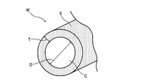
ここで、本実施形態に係るレーザ加工システム100において、加工対象物として用いられる導線Wの構成について、図5を参照しつつ説明する。当該導線Wは、電気を伝導する為の線であり、芯線Cと、被覆層Eとを有して構成されている。芯線Cは、電気伝導性を有する金属(例えば、銅、アルミ等)によって、芯線外径Dを有する線材として形成されている。被覆層Eは、絶縁性を有する樹脂材(例えば、ポリウレタン、ポリエステル等)によって、パルスレーザLを透過可能に構成されており、芯線Cを絶縁・保護する為に配設されている。当該被覆層Eは、所定の被覆層厚Tをもって、芯線Cの外周面を被覆している。
(Construction of conducting wire W)
Here, in the
尚、以下の説明においては、導線Wの径方向に沿ったパルスレーザLの走査方向を「主走査方向」とし、導線Wの軸方向(即ち、主走査方向に直交する方向)を「副走査方向」とする。そして、本実施形態における「主走査方向」は、本発明における第1方向に相当し、「副走査方向」は、本発明における第2方向に相当する。 In the following description, the scanning direction of the pulse laser L along the radial direction of the conducting wire W is referred to as “main scanning direction”, and the axial direction of the conducting wire W (that is, the direction orthogonal to the main scanning direction) is referred to as “sub-scanning”. Direction. The “main scanning direction” in the present embodiment corresponds to the first direction in the present invention, and the “sub-scanning direction” corresponds to the second direction in the present invention.
(導線Wにおける被覆層Eの除去加工に関する基本的工程)
続いて、本実施形態に係るレーザ加工システム100において、データ作成装置7により作成された加工データに基づいて、導線Wに対して実行される被覆層Eの除去加工の内容について説明する。
(Basic process for removing the coating layer E from the conductor W)
Subsequently, in the
本実施形態において、データ作成装置7により作成される加工データは、第1工程と、第2工程を含んでおり、第1工程の後、第2工程を実行するように規定されている。加工データに基づく第1工程においては、レーザ加工装置1は、レーザヘッド部3から出射されたパルスレーザLによって、導線Wの芯線Cに対して所定の第1入熱量を付与しつつ、第1走査速度(例えば、10(mm/s))で主走査方向へ走査させる主走査を、副走査方向へ異なる位置で複数回走査させるように制御される。
In the present embodiment, the processing data created by the
この第1工程を実行することによって、パルスレーザLは、導線Wの被覆層Eを透過して、芯線Cと被覆層Eとの界面を起点として、芯線Cを構成する金属に入熱することで、被覆層Eの溶融や脆化を発生させる。第1工程が実行されることで、被覆層Eの溶融や脆化が発生し、被覆層Eを膨張させるようにして、芯線Cの外周面から被覆層Eを剥離させることができる。 By executing this first step, the pulse laser L passes through the coating layer E of the conducting wire W and heats the metal constituting the core wire C starting from the interface between the core wire C and the coating layer E. Thus, melting or embrittlement of the coating layer E occurs. By performing the first step, melting or embrittlement of the coating layer E occurs, and the coating layer E can be peeled from the outer peripheral surface of the core wire C so as to expand the coating layer E.
第1工程に続いて実行される第2工程では、レーザ加工装置1は、レーザヘッド部3から出射されたパルスレーザLによって、前記第1入熱量よりも小さな第2入熱量を与えつつ、パルスレーザLを、前記第1走査速度よりも高速な第2走査速度(例えば、1500(mm/s))で、副走査方向へ走査させる副走査を、前記主走査方向に異なる方向に異なる位置で複数回走査させるように制御される。第2工程における副走査のうち、少なくとも1本の副走査が、主走査方向に異なる位置で走査されていればよい。つまり、第2工程における副走査の一部は同じ位置を走査してもよい。
In the second step that is executed following the first step, the
そして、この第2工程を実行させることで、パルスレーザLは、第1入熱量よりも小さな第2入熱量をもって副走査を行う為、被覆層Eの溶融や変性を発生させることなく、より高速な第2走査速度で副走査を行うことで、溶融や脆化によって芯線C表面から離間した被覆層Eを効率よく飛散させることができる。 By executing this second step, the pulse laser L performs sub-scanning with a second heat input that is smaller than the first heat input, so that the coating layer E does not melt or denature, resulting in higher speed. By performing the sub-scanning at the second scanning speed, the coating layer E separated from the surface of the core wire C by melting or embrittlement can be efficiently scattered.
本実施形態に係るレーザ加工システム100においては、データ作成装置7により作成された加工データは、第1工程と、第2工程を含んでおり、第1工程の後、第2工程を実行するように規定されている為、第1工程による溶融や脆化によって芯線C表面から離間した被覆層Eを、第2工程によって効率よく飛散させることができ、もって、レーザ加工装置1に、導線Wから被覆層Eを除去させることができる。
In the
(加工データ作成処理プログラムの処理内容)
次に、本実施形態に係るデータ作成装置7において、上述した第1工程及び第2工程を含む加工データを作成する際に実行される加工データ作成処理プログラムの処理内容について、図4を参照しつつ詳細に説明する。当該加工データ作成処理プログラムは、データ作成装置7のHDD75に格納されており、CPU71によって実行される。
(Processing content creation processing program content)
Next, with reference to FIG. 4, the processing content of the machining data creation processing program executed when creating the machining data including the first step and the second step described above in the
図4に示すように、加工データ作成処理プログラムの実行を開始すると、CPU71は、先ず、導線Wに関する種々の構成を示す導線情報を入力する為の導線情報設定ウィンドウ80を、液晶ディスプレイ77に表示する(S1)。導線情報設定ウィンドウ80を液晶ディスプレイ77に表示した後、CPU71は、S2に処理を移行する。
As shown in FIG. 4, when the execution of the machining data creation processing program is started, the CPU 71 first displays on the liquid crystal display 77 a conducting wire
(導線情報設定ウィンドウ80の構成)
ここで、液晶ディスプレイ77上に表示される導線情報設定ウィンドウ80について、図面を参照しつつ詳細に説明する。図6に示すように、導線情報設定ウィンドウ80は、被覆層材質設定部81と、芯線材質設定部82と、被覆層厚設定部83と、芯線外径設定部84と、加工所要時間設定部85と、決定ボタン86とを有している。
(Configuration of Conductor Information Setting Window 80)
Here, the conducting wire
被覆層材質設定部81は、導線情報の一つとして、被覆層Eを構成する材質を入力・設定する際に用いられる。本実施形態において、被覆層材質設定部81は、被覆層Eの材質として、例えば、「UEW(ポリウレタン銅線)」「PEW(ポリエステル銅線)」「HMW(ポリアミドイミド銅線)」等を選択可能に構成されている。従って、ユーザは、データ作成装置7の入力操作部76を用いて、導線情報設定ウィンドウ80の被覆層材質設定部81に対する操作を行うことで、導線Wにおける被覆層Eの材質を、導線情報の一つとして設定し得る。
The covering layer
芯線材質設定部82は、導線情報の一つとして、芯線Cを構成する材質を入力・設定する際に用いられる。本実施形態において、芯線材質設定部82は、芯線Cの材質として、例えば、「銅」「アルミ」等を選択可能に構成されている。従って、ユーザは、データ作成装置7の入力操作部76を用いて、導線情報設定ウィンドウ80の芯線材質設定部82に対する操作を行うことで、導線Wにおける芯線Cの材質を、導線情報の一つとして設定し得る。
The core wire
被覆層厚設定部83は、導線情報の一つとして、導線Wにおける被覆層Eの厚みである被覆層厚Tを入力・設定する際に用いられる。本実施形態において、被覆層厚設定部83は、「薄い(例えば、0.1mm以下)」「中間(例えば、0.1mmよりも大きく、0.2mm以下)」「厚い(例えば、0.2mmよりも大きく、0.5mm以下)」の3段階から、被覆層厚Tを選択可能に構成されている。従って、ユーザは、データ作成装置7の入力操作部76を用いて、導線情報設定ウィンドウ80の被覆層厚設定部83に対する操作を行うことで、導線Wにおける被覆層厚Tを、導線情報の一つとして設定し得る。
The covering layer
芯線外径設定部84は、導線情報の一つとして、導線Wにおける芯線Cの外径である芯線外径Dを入力・設定する際に用いられる。本実施形態において、芯線外径設定部84は、導線Wの芯線Cについての芯線外径Dの数値を入力可能に構成されている。従って、ユーザは、データ作成装置7の入力操作部76を用いて、導線情報設定ウィンドウ80の芯線外径設定部84に、芯線外径Dを入力することで、導線Wにおける芯線外径Dを、導線情報の一つとして設定し得る。
The core wire outer
加工所要時間設定部85は、導線情報の一つとして、導線Wにおける被覆層Eの除去に関する加工所要時間を入力・設定する際に用いられる。加工所要時間設定部85は、「標準」を含む異なる時間から、加工所要時間を選択可能に構成されている。従って、ユーザは、データ作成装置7の入力操作部76を用いて、導線情報設定ウィンドウ80の加工所要時間設定部85に対する操作を行うことで、加工所要時間を、導線情報の一つとして設定し得る。
The required processing
決定ボタン86は、被覆層材質設定部81、芯線材質設定部82、被覆層厚設定部83、芯線外径設定部84、加工所要時間設定部85に入力された導線情報の入力を確定する際に操作される。従って、本実施形態においては、CPU71は、決定ボタン86の入力操作が行われた時点で、被覆層材質設定部81、芯線材質設定部82、被覆層厚設定部83、芯線外径設定部84、加工所要時間設定部85に入力された内容を導線情報としてRAM72に格納し、S2に処理を移行する。
The
S2においては、CPU71は、入力操作部76による入力操作に基づいて、導線情報設定ウィンドウ80の被覆層材質設定部81を用いて、被覆層Eの材質を導線情報の一つとして受け付けたか否かを判断する。被覆層Eの材質を導線情報の一つとして受け付けた場合(S2:YES)、CPU71は、S3に処理を移行する。一方、被覆層Eの材質を導線情報の一つとして受け付けていない場合(S2:NO)、CPU71は、被覆層Eの材質を導線情報として受け付けるまで、処理を待機する。
In S <b> 2, whether or not the CPU 71 has received the material of the coating layer E as one of the conductor information using the coating layer
S3では、CPU71は、S2で導線情報として受け付けた被覆層Eの材質に関する情報と、被覆層材質テーブル(図7参照)に基づいて、導線Wにおける被覆層Eの除去加工を行う際に、パルスレーザLによって芯線Cに入熱される基礎入熱量を設定する。設定した基礎入熱量をRAM72に格納した後、CPU71は、S4に処理を移行する。
In S3, the CPU 71 performs a pulse when removing the coating layer E from the conductor W based on the information on the material of the coating layer E received as the conductor information in S2 and the coating layer material table (see FIG. 7). A basic heat input amount that is input to the core C by the laser L is set. After storing the set basic heat input amount in the
(被覆層材質テーブルの内容)
ここで、S3において、基礎入熱量を設定する際に参照される被覆層材質テーブルの内容について、図7を参照しつつ詳細に説明する。図7に示すように、被覆層材質テーブルは、被覆層Eの材質に対して、当該導線Wから被覆層Eを除去する際のパルスレーザLによる基礎入熱量を対応付けて構成されている。被覆層Eの材質は、被覆層Eの耐熱性に直接的に関連する。被覆層Eが耐熱性の高い材質で構成されている場合、パルスレーザLによって被覆層Eの溶融や脆化等を発生させる為には、より大きな入熱量を付与する必要が生じる。一方、被覆層Eが耐熱性の低い材質で構成されている場合、小さな入熱量を付与すれば、パルスレーザLによって被覆層Eの溶融や脆化等を発生させることができる。即ち、本実施形態に係る被覆層材質テーブルは、被覆層Eの材質ごとの耐熱性の高低に応じて、当該導線Wから被覆層Eを除去する際のパルスレーザLによる基礎入熱量を対応付けて構成されている。PEWに対応する入熱量は、例えば、スポット径内に入る見かけの投入エネルギーであり、3.3(mJ/PULSE)である。UEWに対応する入熱量は、例えば、スポット径内に入る見かけの投入エネルギーであり、2.8(mJ/PULSE)である。HMWに対応する入熱量は、例えば、スポット径内に入る見かけの投入エネルギーであり、4.7(mJ/PULSE)である。
(Content of coating layer material table)
Here, in S3, the contents of the coating layer material table referred to when setting the basic heat input will be described in detail with reference to FIG. As shown in FIG. 7, the coating layer material table is configured by associating the material of the coating layer E with the basic heat input by the pulse laser L when removing the coating layer E from the conductor W. The material of the coating layer E is directly related to the heat resistance of the coating layer E. When the coating layer E is made of a material having high heat resistance, in order to cause the coating layer E to melt or become brittle by the pulse laser L, it is necessary to apply a larger amount of heat input. On the other hand, when the coating layer E is made of a material having low heat resistance, the pulse layer L can cause melting or embrittlement of the coating layer E if a small heat input is applied. That is, the coating layer material table according to the present embodiment associates the basic heat input by the pulse laser L when removing the coating layer E from the conductor W in accordance with the heat resistance level of each material of the coating layer E. Configured. The amount of heat input corresponding to PEW is, for example, the apparent input energy that falls within the spot diameter, and is 3.3 (mJ / PULSE). The amount of heat input corresponding to UEW is, for example, the apparent input energy that falls within the spot diameter, and is 2.8 (mJ / PULSE). The amount of heat input corresponding to HMW is, for example, the apparent input energy that falls within the spot diameter, and is 4.7 (mJ / PULSE).
従って、S3においては、CPU71は、S2で導線情報として受け付けた被覆層Eの材質に関する情報と、被覆層材質テーブル(図7参照)を参照して、基礎入熱量を設定することによって、被覆層Eの材質に応じた適切な基礎入熱量を設定する。 Accordingly, in S3, the CPU 71 sets the basic heat input amount with reference to the information on the material of the coating layer E received as the conductive wire information in S2 and the coating layer material table (see FIG. 7). Set an appropriate basic heat input according to the material of E.
S4では、CPU71は、入力操作部76による入力操作に基づいて、導線情報設定ウィンドウ80の芯線材質設定部82を用いて、芯線Cの材質を導線情報の一つとして受け付けたか否かを判断する。芯線Cの材質を導線情報の一つとして受け付けた場合(S4:YES)、CPU71は、S5に処理を移行する。一方、芯線Cの材質を導線情報の一つとして受け付けていない場合(S4:NO)、CPU71は、芯線Cの材質を導線情報として受け付けるまで、処理を待機する。
In S <b> 4, the CPU 71 determines whether or not the material of the core wire C is received as one of the conductor information using the core wire
S5においては、CPU71は、導線情報の一つとして受け付けた芯線Cの材質に関する情報と、芯線材質テーブル(図8参照)に基づいて、入熱量補正処理を実行することで、芯線Cの材質に基づいて、パルスレーザLによって芯線Cに入熱される入熱量を補正する。具体的には、入熱量補正処理(S5)では、CPU71は、S4で導線情報として受け付けた芯線Cの材質に関する情報と、芯線材質テーブル(図8参照)に基づいて、芯線Cの材質に対応する補正倍率を特定し、S3で設定された基礎入熱量に対して、特定した補正倍率を乗算することで、パルスレーザLによって芯線Cに入熱される入熱量を、被覆層E及び芯線Cに対応した適切な入熱量に補正する。補正した入熱量をRAM72に格納した後、CPU71は、S6に処理を移行する。
In S5, the CPU 71 executes the heat input correction process based on the information on the material of the core wire C received as one of the conductive wire information and the core wire material table (see FIG. 8), so that the material of the core wire C is changed. Based on this, the amount of heat input to the core wire C by the pulse laser L is corrected. Specifically, in the heat input correction process (S5), the CPU 71 corresponds to the material of the core wire C based on the information on the material of the core wire C received as the conductive wire information in S4 and the core wire material table (see FIG. 8). By specifying the correction magnification to be performed and multiplying the basic heat input amount set in S3 by the specified correction magnification, the heat input amount that is input to the core wire C by the pulse laser L is applied to the coating layer E and the core wire C. Correct to the appropriate heat input. After storing the corrected heat input amount in the
(芯線材質テーブルの内容)
次に、S5において、入熱量を補正する為の補正倍率を特定する際に参照される芯線材質テーブルの内容について、図8を参照しつつ詳細に説明する。図8に示すように、芯線材質テーブルは、芯線Cの材質に対して、S3で設定された基礎入熱量を補正する為の補正倍率を対応付けて構成されている。当該補正倍率は、芯線Cの材質に係る密度と、比熱と、吸収率に基づいて算出される。具体的には、各補正倍率は、芯線Cの材質に係る密度と、比熱と、吸収率を乗算した値の逆数を取り、銅を基準として規格化して特定される。
(Content of core wire material table)
Next, in S5, the contents of the core wire material table that is referred to when specifying the correction magnification for correcting the heat input will be described in detail with reference to FIG. As shown in FIG. 8, the core wire material table is configured by associating the correction factor for correcting the basic heat input amount set in S <b> 3 with the material of the core wire C. The correction magnification is calculated based on the density, specific heat, and absorption rate related to the material of the core C. Specifically, each correction magnification is specified by taking the reciprocal of a value obtained by multiplying the density, specific heat, and absorptance related to the material of the core C, and standardizing with reference to copper.
従って、S5においては、CPU71は、S4で導線情報として受け付けた芯線Cの材質に関する情報と、芯線材質テーブル(図8参照)を参照して、芯線Cの材質に対応する補正倍率を特定し、基礎入熱量に対して特定した補正倍率を乗算することで、被覆層E及び芯線Cの材質に応じた適切なパルスレーザLの入熱量を設定することができる。 Therefore, in S5, the CPU 71 specifies the correction magnification corresponding to the material of the core wire C with reference to the information on the material of the core wire C received as the conductive wire information in S4 and the core wire material table (see FIG. 8). By multiplying the basic heat input by the specified correction magnification, it is possible to set an appropriate heat input of the pulse laser L according to the material of the coating layer E and the core wire C.
S6に移行すると、CPU71は、入力操作部76による入力操作に基づいて、導線情報設定ウィンドウ80の被覆層厚設定部83を用いて、被覆層厚Tに関する情報の入力を導線情報の一つとして受け付けたか否かを判断する。被覆層厚Tに関する情報を導線情報の一つとして受け付けた場合(S6:YES)、CPU71は、S7に処理を移行する。一方、被覆層厚Tに関する情報を導線情報の一つとして受け付けていない場合(S6:NO)、CPU71は、被覆層厚Tに関する情報を導線情報として受け付けるまで、処理を待機する。
In S6, the CPU 71 uses the covering layer
S7では、CPU71は、導線情報の一つとして受け付けた被覆層厚Tに関する情報と、被覆層厚テーブル(図9参照)に基づいて、入熱量補正処理を実行することで、被覆層厚Tに基づいて、パルスレーザLによって芯線Cに入熱される入熱量を補正する。具体的には、入熱量補正処理(S7)では、CPU71は、S6で導線情報として受け付けた被覆層厚Tに関する情報と、被覆層厚テーブル(図9参照)に基づいて、被覆層厚Tに対応する補正倍率を特定し、S5で補正された入熱量に対して、特定した補正倍率を乗算することで、パルスレーザLによって芯線Cに入熱される入熱量を、被覆層E、芯線C及び被覆層厚Tに対応した適切な入熱量に補正する。補正した入熱量をRAM72に格納した後、CPU71は、S8に処理を移行する。
In S7, the CPU 71 sets the coating layer thickness T by executing the heat input correction process based on the information regarding the coating layer thickness T received as one of the conductive wire information and the coating layer thickness table (see FIG. 9). Based on this, the amount of heat input to the core wire C by the pulse laser L is corrected. Specifically, in the heat input correction process (S7), the CPU 71 sets the coating layer thickness T based on the information related to the coating layer thickness T received as the conductor information in S6 and the coating layer thickness table (see FIG. 9). The corresponding correction magnification is specified, and the heat input amount corrected in S5 is multiplied by the specified correction magnification, so that the heat input amount to be input to the core wire C by the pulse laser L is changed to the coating layer E, the core wire C, and The heat input is corrected to an appropriate amount corresponding to the coating layer thickness T. After storing the corrected heat input amount in the
(被覆層厚テーブルの内容)
続いて、S7において、入熱量を補正する為の補正倍率を特定する際に参照される被覆層厚テーブルの内容について、図9を参照しつつ詳細に説明する。図9に示すように、被覆層厚テーブルは、被覆層厚Tに対して、S5で補正された入熱量を更に補正する為の補正倍率を対応付けて構成されている。被覆層厚Tは、被覆層Eにおける熱の伝導しやすさや、被覆層Eに発生した亀裂の進展しやすさに影響する為、被覆層厚Tに対して夫々補正倍率を対応付けることによって、被覆層厚Tに対応する入熱量をもって、被覆層Eの除去加工を行い得る。
(Content of coating layer thickness table)
Subsequently, in S7, the content of the coating layer thickness table referred to when specifying the correction magnification for correcting the heat input will be described in detail with reference to FIG. As shown in FIG. 9, the coating layer thickness table is configured by associating the coating layer thickness T with a correction magnification for further correcting the heat input amount corrected in S5. Since the coating layer thickness T affects the ease of heat conduction in the coating layer E and the ease of cracks occurring in the coating layer E, the coating layer thickness T is determined by associating the correction factor with the coating layer thickness T. The removal process of the coating layer E can be performed with a heat input corresponding to the layer thickness T.
従って、S7においては、CPU71は、S6で導線情報として受け付けた被覆層厚Tに関する情報と、被覆層厚テーブル(図9参照)を参照して、被覆層厚Tに対応する補正倍率を特定し、S5で補正された入熱量に対して特定した補正倍率を乗算することで、被覆層E、芯線Cの材質及び被覆層厚Tに応じた適切なパルスレーザLの入熱量を設定することができる。 Accordingly, in S7, the CPU 71 specifies the correction magnification corresponding to the coating layer thickness T with reference to the information regarding the coating layer thickness T received as the conductor information in S6 and the coating layer thickness table (see FIG. 9). By multiplying the heat input amount corrected in S5 by the specified correction magnification, an appropriate heat input amount of the pulse laser L according to the material of the coating layer E and the core wire C and the coating layer thickness T can be set. it can.
S8に移行すると、CPU71は、入力操作部76による入力操作に基づいて、導線情報設定ウィンドウ80の芯線外径設定部84を用いて、芯線外径Dに関する情報を導線情報の一つとして受け付けたか否かを判断する。芯線外径Dに関する情報を導線情報の一つとして受け付けた場合(S8:YES)、CPU71は、S9に処理を移行する。一方、芯線外径Dに関する情報を導線情報の一つとして受け付けていない場合(S8:NO)、CPU71は、芯線外径Dに関する情報を導線情報として受け付けるまで、処理を待機する。
When the process proceeds to S8, the CPU 71 has received information about the core wire outer diameter D as one of the conductor information using the core wire outer
S9においては、CPU71は、導線情報として受け付けた芯線外径Dに関する情報に基づいて、芯線Cの主走査方向におけるパルスレーザLによる入熱量の分布を補正する。具体的には、CPU71は、芯線外径Dに関する情報に基づいて、主走査方向における芯線Cの外表面に対して、均一に入熱可能な入熱量の分布を補正する。 In S <b> 9, the CPU 71 corrects the distribution of heat input by the pulse laser L in the main scanning direction of the core wire C based on the information regarding the core wire outer diameter D received as the conductive wire information. Specifically, the CPU 71 corrects the distribution of heat input that can be uniformly input to the outer surface of the core wire C in the main scanning direction based on the information about the core wire outer diameter D.
ここで、芯線Cは、図5に示すように、副走査方向に伸びる略円柱形状を為している。そして、上述したように、レーザ加工装置1は、加工容器内に配置された芯線Cに対してパルスレーザLを照射する為、パルスレーザLは、芯線Cの略真上から照射されることになる(図1参照)。この場合において、パルスレーザLの走査を主走査方向に均等なピッチで入熱すると、芯線Cの外周面は曲面である為、芯線C外周面における入熱量は、主走査方向(径方向)における内外位置に応じて変動してしまう。又、パルスレーザLが被覆層Eを透過して界面に到達するまでの距離は、導線Wの径方向における位置に対応して変化し、芯線外径Dの影響を受ける。
Here, the core wire C has a substantially cylindrical shape extending in the sub-scanning direction, as shown in FIG. And as above-mentioned, since the
この為、入熱量分布の補正(S9)を実行することで、具体的には主走査方向におけるパルスレーザLの走査ピッチ(走査軌跡LSの間隔)を、芯線外径Dに応じて、芯線Cの径方向外側に向かうにつれて小さくする補正する(図10(A)(B)参照)。これにより、図10(C)に示すように、芯線Cの外周面を展開すると、パルスレーザLの走査ピッチ(走査軌跡LSの間隔)を、芯線Cの外周面に対して均等なピッチに補正することができ、芯線C外周面に対して均一に入熱することができる。このようにして、芯線Cの主走査方向におけるパルスレーザLによる入熱量の分布を補正した後、CPU71は、S10に処理を移行する。 Therefore, by executing the correction (S9) of the heat input distribution, specifically, the scanning pitch of the pulse laser L in the main scanning direction (interval of the scanning trajectory LS) is changed according to the core wire outer diameter D to the core wire C. The correction is made to decrease as it goes outward in the radial direction (see FIGS. 10A and 10B). 10C, when the outer peripheral surface of the core wire C is developed, the scanning pitch of the pulse laser L (interval of the scanning locus LS) is corrected to a uniform pitch with respect to the outer peripheral surface of the core wire C. It is possible to heat input uniformly to the outer peripheral surface of the core wire C. In this way, after correcting the distribution of heat input by the pulse laser L in the main scanning direction of the core C, the CPU 71 shifts the process to S10.
S10に移行すると、CPU71は、導線情報として受け付けた芯線外径Dに基づいて、第2工程における複数の副走査を行う際に、主走査方向への走査ピッチの最小値を設定する。具体的には、CPU71は、芯線Cの主走査方向へ異なる位置で、2回の副走査を実行可能なように、第2工程における主走査方向への走査ピッチを設定する。その後、CPU71は、S11に処理を移行する。 After shifting to S10, the CPU 71 sets the minimum value of the scanning pitch in the main scanning direction when performing a plurality of sub-scans in the second step based on the core wire outer diameter D received as the conductive wire information. Specifically, the CPU 71 sets the scanning pitch in the main scanning direction in the second step so that two sub-scans can be executed at different positions in the main scanning direction of the core C. Thereafter, the CPU 71 shifts the processing to S11.
ここで、S10の処理に関して説明する。上述したように、第2工程は、第2走査速度で副走査方向に高速走査することで、第1工程を経て芯線C表面から剥離した被覆層Eを飛散させて除去することに重点を置いた工程である。従って、第2工程では、副走査方向へのパルスレーザLの高速走査である、副走査を、主走査方向(即ち、芯線Cの径方向)に異なる位置で複数回行うことが望ましい。S10を実行することで、芯線外径Dに対応する第2工程における主走査方向の走査ピッチを設定することができるので、第2工程において、芯線Cに対して、確実に、パルスレーザLの副走査を複数回行うことが可能となる。 Here, the process of S10 will be described. As described above, the second step focuses on removing the coating layer E peeled off from the surface of the core wire C through the first step by performing high-speed scanning in the sub-scanning direction at the second scanning speed. It is a process. Therefore, in the second step, it is desirable to perform sub-scanning, which is high-speed scanning of the pulse laser L in the sub-scanning direction, a plurality of times at different positions in the main scanning direction (that is, the radial direction of the core line C). By executing S10, the scanning pitch in the main scanning direction in the second step corresponding to the core wire outer diameter D can be set. Sub-scanning can be performed a plurality of times.
S11では、CPU71は、入力操作部76による入力操作に基づいて、導線情報設定ウィンドウ80の加工所要時間設定部85を用いて、加工所要時間の入力を受け付けたか否かを判断する。加工所要時間の入力を受け付けた場合(S11:YES)、CPU71は、S12に処理を移行する。一方、加工所要時間の入力を受け付けていない場合(S11:NO)、CPU71は、加工所要時間の入力を受け付けるまで、処理を待機する。
In S <b> 11, based on the input operation by the
S12においては、CPU71は、加工パラメータ設定処理に移行し、導線Wにおける被覆層Eの除去加工に関して、ユーザ所望の加工パラメータの設定を行う。加工パラメータ設定処理(S12)においては、CPU71は、HDD75から加工パラメータ設定処理プログラムを実行する。
In S <b> 12, the CPU 71 shifts to a processing parameter setting process and sets processing parameters desired by the user regarding the removal processing of the coating layer E on the conductive wire W. In the machining parameter setting process (S <b> 12), the CPU 71 executes a machining parameter setting process program from the
(加工パラメータ設定処理プログラムの処理内容)
ここで、加工パラメータ設定処理(S12)で実行される加工パラメータ設定処理プログラムの処理内容について、図11を参照しつつ詳細に説明する。加工パラメータ設定処理(S12)に移行すると、CPU71は、先ず、導線Wにおける被覆層Eの除去加工に関して、ユーザ所望の加工パラメータを設定する為のパラメータ設定ウィンドウ90を、液晶ディスプレイ77に表示する(S21)。パラメータ設定ウィンドウ90を、液晶ディスプレイ77に表示した後、CPU71は、S22に処理を移行する。
(Processing contents of machining parameter setting processing program)
Here, the processing content of the processing parameter setting processing program executed in the processing parameter setting processing (S12) will be described in detail with reference to FIG. After shifting to the processing parameter setting process (S12), the CPU 71 first displays a
(導線情報設定ウィンドウ80の構成)
ここで、液晶ディスプレイ77上に表示されるパラメータ設定ウィンドウ90について、図面を参照しつつ詳細に説明する。図12に示すように、パラメータ設定ウィンドウ90は、走査パターン設定部91と、走査間隔設定部92と、走査速度設定部93と、反復回数設定部94と、レーザ強度設定部95と、設定完了ボタン96とを有している。
(Configuration of Conductor Information Setting Window 80)
Here, the
走査パターン設定部91は、第1工程における複数回の主走査を行う際の走査パターンを設定する際に用いられ、「時間優先」という走査パターンと、「品質優先」という走査パターンとを選択可能に構成されている。従って、ユーザは、データ作成装置7の入力操作部76を用いて、パラメータ設定ウィンドウ90の走査パターン設定部91に対する操作を行うことで、加工パラメータの一つとして、所望の走査パターンを設定し得る。
The scan
ここで、図12に示すように、「時間優先」という走査パターンは、パルスレーザLを照射しつつ、主走査方向の一方側から他方側へ走査する主走査を行った後、パルスレーザLの照射を継続して、主走査方向の他方側から一方側へ戻りつつ副走査方向へ異なる位置へ移動させる(主走査方向と副走査方向に関して斜めに移動させる)走査パターンである。この「時間優先」に係る走査パターンでは、複数回の主走査の間において、主走査方向と副走査方向に関して斜めに移動させる過程でも、パルスレーザLによる入熱が行われる為、第1工程に要する時間を短縮することができる。尚、この場合、第1工程における芯線Cに対する入熱は不均一になってしまう為、被覆層Eの除去加工に関する加工品質を低下してしまう虞がある。 Here, as shown in FIG. 12, the scan pattern of “time priority” is that the pulse laser L is irradiated with the pulse laser L and the main scan is performed from one side to the other side in the main scan direction. This is a scanning pattern in which irradiation is continued and moved to different positions in the sub-scanning direction while returning from the other side in the main scanning direction to one side (moved obliquely with respect to the main scanning direction and the sub-scanning direction). In the scanning pattern related to this “time priority”, heat input by the pulse laser L is performed even in the process of moving obliquely with respect to the main scanning direction and the sub-scanning direction during a plurality of main scans. The time required can be shortened. In this case, since heat input to the core wire C in the first step becomes non-uniform, there is a possibility that the processing quality related to the removal processing of the coating layer E may be deteriorated.
一方、「品質優先」という走査パターンは、パルスレーザLを照射しつつ、主走査方向の一方側から他方側へ走査する主走査を行った後、パルスレーザLの照射を停止して、副走査方向の異なる位置へ移動させ、その後、パルスレーザLを照射しつつ、主走査方向の他方側から一方側へ走査する主走査を行う走査パターンである。この「品質優先」に係る走査パターンによれば、第1工程において、パルスレーザLによる芯線Cに対する入熱を均一に行うことができる。尚、この場合、第1工程を行う際に主走査方向及び副走査方向への経路が長くなり、且つ、パルスレーザLの出射に関するON・OFFの切替が生じる為、第1工程に要する時間が長期化する場合がある。 On the other hand, in the scanning pattern of “quality priority”, the main laser scanning from one side to the other side in the main scanning direction is performed while irradiating the pulse laser L, and then the irradiation of the pulse laser L is stopped and the sub scanning is performed. This is a scanning pattern in which main scanning is performed in which scanning is performed from the other side in the main scanning direction to one side while moving to different positions and then irradiating the pulse laser L. According to the scanning pattern related to “quality priority”, heat input to the core wire C by the pulse laser L can be performed uniformly in the first step. In this case, when the first step is performed, the path in the main scanning direction and the sub-scanning direction becomes long, and ON / OFF switching related to the emission of the pulse laser L occurs. May be longer.
走査間隔設定部92は、加工パラメータとして、導線Wに対してパルスレーザLの走査を行う場合の走査間隔(即ち、走査ピッチ)を入力・設定する際に用いられ、所謂、スライダによって構成されている。走査間隔設定部92は、入力操作部76の操作を受け付けることで、最小値から最大値の数値範囲の間における任意の数値を設定することができる。本実施形態において、走査間隔設定部92における最小値は、例えばパルスレーザLのビーム径であり、例えば、50(μm)である。第1工程における最大値は、被覆層Eの除去加工が可能な上限値であり、例えば、150(μm)である。そして、第2工程における最大値は、芯線外径Dの1/2である。従って、ユーザは、データ作成装置7の入力操作部76を用いて、パラメータ設定ウィンドウ90の走査間隔設定部92を操作することで、所望の走査間隔を加工パラメータとして設定することができる。
The scanning
走査速度設定部93は、加工パラメータとして、第1工程における主走査方向への走査速度(即ち、第1走査速度)を入力・設定する際に用いられ、所謂、スライダによって構成されている。走査速度設定部93は、入力操作部76の操作を受け付けることで、最小値から最大値の数値範囲の間における任意の数値を設定することができる。本実施形態において、走査速度設定部93における最小値は、被覆層Eの除去加工の結果、芯線C表面に、酸化による黒変が生じることがない程度の走査速度を示し、走査速度設定部93の最大値は、被覆層Eの除去加工が可能な上限値であり、例えば、20(mm/s)である。従って、ユーザは、データ作成装置7の入力操作部76を用いて、パラメータ設定ウィンドウ90の走査速度設定部93を操作することで、所望の第1走査速度を加工パラメータとして設定することができる。ここで、本実施形態とは異なるが、走査速度が所定の速度に固定されていてもよい。例えば、第2走査の走査速度は、ある程度以上では除去に対する影響がないとして、第2走査の走査速度が1500(mm/s)に固定されていてもよい。
The scanning
反復回数設定部94は、加工パラメータとして、第2工程における副走査の反復回数を入力・設定する際に用いられ、所謂、スライダによって構成されている。反復回数設定部94は、入力操作部76の操作を受け付けることで、最小値から最大値の数値範囲の間における任意の数値を設定することができる。本実施形態において、反復回数設定部94における最小値は、被覆層Eの除去加工が可能な下限値であり、例えば、10回を示す。そして、反復回数設定部94の最大値は、被覆層Eの除去加工の結果、芯線C表面に、酸化による黒変が生じることがない程度の反復回数を示す。従って、ユーザは、データ作成装置7の入力操作部76を用いて、パラメータ設定ウィンドウ90の反復回数設定部94を操作することで、加工パラメータとして、第2工程における副走査の反復回数を、所望の回数に設定することができる。ここで、本実施形態とは異なるが、走査の回数が所定の回数に固定されていてもよい。例えば、第1走査の回数が1回に固定されていてもよい。
The iteration
レーザ強度設定部95は、加工パラメータとして、被覆層Eの除去加工におけるパルスレーザLのレーザ強度を入力・設定する際に用いられ、所謂、スライダによって構成されている。レーザ強度設定部95は、入力操作部76の操作を受け付けることで、最小値から最大値の数値範囲の間における任意の数値を設定することができる。レーザ強度設定部95における最大値は、レーザ加工装置1が出力可能なパルスレーザLのレーザ強度の最大値を示し、本実施形態においては、5(W)である。そして、レーザ強度設定部95における最小値は、例えば、4(W)である。従って、ユーザは、データ作成装置7の入力操作部76を用いて、パラメータ設定ウィンドウ90のレーザ強度設定部95を操作することで、加工パラメータとして、被覆層Eの除去加工におけるパルスレーザLのレーザ強度を、所望のレーザ強度に設定することができる。
The laser
設定完了ボタン96は、走査パターン設定部91、走査間隔設定部92、走査速度設定部93、反復回数設定部94、レーザ強度設定部95に入力された加工パラメータの設定を確定する際に操作される。
The
S22においては、CPU71は、設定入力受付処理を実行することにより、パラメータ設定ウィンドウ90を構成する各部に対する入力を受け付ける。具体的には、CPU71は、データ作成装置7の入力操作部76からの操作信号に基づいて、走査パターン設定部91、走査間隔設定部92、走査速度設定部93、反復回数設定部94、レーザ強度設定部95、設定完了ボタン96に対する入力を受け付ける。その後、CPU71は、S23に処理を移行する。
In S <b> 22, the CPU 71 receives an input to each unit constituting the
S23に移行すると、CPU71は、入力操作部76による入力操作に基づいて、パラメータ設定ウィンドウ90の設定完了ボタン96に対する入力操作が行われたか否かを判断する。設定完了ボタン96に対する入力操作が行われた場合(S23:YES)、CPU71は、S24に処理を移行する。一方、設定完了ボタン96に対する入力操作が行われていない場合(S23:NO)、CPU71は、設定入力受付処理(S22)に処理を戻し、走査パターン設定部91、走査間隔設定部92、走査速度設定部93、反復回数設定部94、レーザ強度設定部95、設定完了ボタン96に対する入力を受け付ける。
In S23, the CPU 71 determines whether or not an input operation has been performed on the
S24では、CPU71は、設定実行処理を実行することで、パラメータ設定ウィンドウ90の各部における設定内容を、各加工パラメータとして確定する。具体的には、CPU71は、設定完了ボタン96の入力操作が行われた時点で、走査パターン設定部91、走査間隔設定部92、走査速度設定部93、反復回数設定部94、レーザ強度設定部95に入力されている内容を、加工パラメータとしてRAM72に格納する。そして、設定実行処理を終了すると、CPU71は、加工パラメータ設定処理プログラムを終了し、データ作成処理プログラム(図4参照)のS13に処理を移行する。
In S <b> 24, the CPU 71 executes setting execution processing to determine the setting contents in each part of the
S13に移行すると、CPU71は、加工実行処理を実行し、導線Wにおける被覆層Eの除去加工の開始を指示する加工開始指示と共に、S1〜S12を経て作成された加工データを、レーザコントローラ5に対して送信する。当該加工データは、S1〜S11までの処理に従って規定された上述した第1工程、第2工程の内容と、S12によって設定された種々の加工パラメータを含んで構成されている。加工開始指示及び加工データを、レーザコントローラ5に対して送信した後、CPU71は、データ作成処理プログラムを終了する。
When the process proceeds to S13, the CPU 71 executes a process execution process, and sends the process data created through S1 to S12 to the
そして、加工実行処理(S13)で送信された加工開始指示及び加工データを受信すると、レーザコントローラ5のCPU61は、受信した加工データに従って、レーザドライバ51及びガルバノドライバ57を制御する。これにより、本実施形態に係るレーザ加工装置1によれば、導線Wにおける被覆層Eの除去加工を、導線Wの構成に対応した態様で、第1工程及び第2工程の順に行うことができ、もって、適切かつ効率の良い導線Wにおける被覆層Eの除去を実現し得る。
When the machining start instruction and the machining data transmitted in the machining execution process (S13) are received, the
以上説明したように、本実施形態に関するデータ作成装置7によれば、データ作成処理プログラム(図4)に従って、導線情報設定ウィンドウ80を用いて入力された導線情報に基づいて、第1工程及び第2工程を含む加工データを作成することができる。
As described above, according to the
加工データに基づく第1工程においては、レーザ加工装置1は、レーザヘッド部3から出射されたパルスレーザLによって、導線Wの芯線Cに対して所定の第1入熱量を付与しつつ、第1走査速度(例えば、10(mm/s))で主走査方向へ走査させる主走査を、副走査方向へ異なる位置で複数回走査させるように制御される。第1工程に続いて実行される第2工程では、レーザ加工装置1は、レーザヘッド部3から出射されたパルスレーザLによって、前記第1入熱量よりも小さな第2入熱量を与えつつ、パルスレーザLを、前記第1走査速度よりも高速な第2走査速度(例えば、1500(mm/s))で、副走査方向へ走査させる副走査を、前記主走査方向に異なる方向に異なる位置で複数回走査させるように制御される。
In the first step based on the processing data, the
当該データ作成装置7によれば、加工データに従って、レーザ加工装置1に第1工程を実行させることで、導線Wにおける芯線Cと被覆層Eの間の界面を起点として、溶融や脆化等を発生させ、被覆層Eを膨張させるようにして芯線C表面から離間させることができる。そして、レーザ加工装置1に第2工程を実行させることで、溶融や脆化によって芯線C表面から離間した被覆層Eを、レーザ光の副走査によって、効率よく飛散させることができる。当該データ作成装置7によれば、データ作成処理プログラム(図4)に従って、加工データを作成して送信することで、レーザ加工装置1に、導線Wにおける被覆層Eの除去加工を、適切かつ効率の良く実行させることができる。
According to the
又、データ作成装置7によれば、導線情報設定ウィンドウ80によって受け付けられた導線情報に基づいて、加工データにおける第1工程、第2工程の内容(パルスレーザLによる入熱量等)を決定して、加工データを作成することができる。当該データ作成装置7によれば、導線情報に基づく導線Wの構成(例えば、芯線C、被覆層Eの材質)に応じた第1工程及び第2工程を、レーザ加工装置1に実行させることができ、もって、適切かつ効率の良い被覆層Eの除去に貢献し得る。
Further, according to the
そして、当該データ作成装置7によれば、導線情報設定ウィンドウ80の被覆層材質設定部81で入力された導線情報としての、被覆層Eの構成材料に関する情報と、被覆層材質テーブル(図7参照)に基づいて、パルスレーザLにおける基礎入熱量を決定することができる(S3)。被覆層Eの構成材料が相違する場合、被覆層Eの物性(例えば、耐熱性等)が異なる為、パルスレーザLによる被覆層Eの溶融や脆化等の生じ易さも相違する。即ち、データ作成装置7によれば、加工データの内容として、導線Wにおける被覆層Eの構成材料に応じた基礎入熱量を設定することができ、もって、適切かつ効率の良い被覆層Eの除去に貢献し得る。
And according to the said
又、当該データ作成装置7によれば、加工データにおけるパルスレーザLによる入熱量を、導線情報設定ウィンドウ80の芯線材質設定部82を用いて入力された芯線Cの材質に関する情報と、芯線材質テーブル(図8参照)に基づいて、パルスレーザLによる入熱量を補正し得る(S5)。芯線Cの構成材料が相違する場合、芯線Cの物性(例えば、吸収率、熱容量、熱伝導率等)が異なる為、パルスレーザLによる芯線Cの加熱の速さも相違する。即ち、当該データ作成装置7によれば、加工データの内容として、導線Wにおける芯線Cの構成材料に応じて、パルスレーザLによる入熱量を補正することができ、もって、適切かつ効率の良い被覆層Eの除去加工に貢献し得る。
Further, according to the
そして、当該データ作成装置7によれば、加工データに規定されたパルスレーザLによる入熱量を、導線情報設定ウィンドウ80の被覆層厚設定部83を用いて入力された被覆層厚Tに関する情報と、被覆層厚テーブル(図9参照)に基づいて補正し得る。パルスレーザLは、被覆層Eを透過した後、芯線C表面と被覆層Eとの間の界面に作用する為、被覆層厚Tは、被覆層Eの除去に関する容易性に影響を与える。即ち、データ作成装置7によれば、加工データの内容として、被覆層厚Tに応じて、パルスレーザLにおける入熱量を補正することができ、もって、適切かつ効率の良い被覆層Eの除去に貢献し得る。
And according to the said
又、当該データ作成装置7によれば、パラメータ設定ウィンドウ90を用いて、種々の加工パラメータの入力・設定することができ、導線Wにおける被覆層Eの除去加工に関する加工パラメータとして、所望のパラメータを設定することができる。即ち、当該データ作成装置7によれば、導線情報設定ウィンドウ80で入力された導線情報(即ち、導線Wの構成)に加えて、パラメータ設定ウィンドウ90で入力された加工パラメータに従って、加工データの内容を決定することができるので、導線Wにおける被覆層Eの除去をユーザ所望の態様で実行させることができる。
Further, according to the
そして、当該データ作成装置7によれば、加工データの内容として、導線情報設定ウィンドウ80の芯線外径設定部84によって受け付けられた芯線外径Dに関する情報に基づいて、芯線Cの径方向(主走査方向)に関して、前記パルスレーザLによる入熱量の分布を補正する(S9)。ここで、パルスレーザLが被覆層Eを透過して界面に到達するまでの距離は、導線Wの径方向における位置に対応して変化し、芯線外径Dの影響を受ける。従って、当該データ作成装置7によれば、芯線外径Dに関する情報に基づいて、前記導線Wの主走査方向(径方向)についてのパルスレーザLによる入熱量の分布を補正することで(S9)、均一に界面効果を発生させることができ、もって、適切かつ効率の良い被覆層Eの除去に貢献し得る。
Then, according to the
又、当該データ作成装置7によれば、導線情報設定ウィンドウ80の芯線外径設定部84によって受け付けられた芯線外径Dに関する情報に基づいて、第2工程における複数回の副走査を行う際の走査ピッチを、芯線C表面に対して均一に入熱可能な走査ピッチに設定することができる(S10)。ここで、芯線C表面と被覆層Eの界面は、曲面状に構成されている為、パルスレーザLの走査ピッチを単純に等間隔としても、芯線C表面においては、パルスレーザLによる入熱の均一性を確保し得ない。この点、データ作成装置7によれば、芯線外径Dに関する情報に基づいて、第2工程における複数回の副走査を行う際の走査ピッチを、芯線C表面に対して均一に入熱可能な走査ピッチに設定できるので、均一に界面効果を発生させることができ、もって、適切かつ効率の良い被覆層Eの除去に貢献し得る。
Further, according to the
そして、データ作成装置7によれば、パラメータ設定ウィンドウ90の走査パターン設定部91を用いて、第1工程におけるパルスレーザLの走査パターンを、「時間優先」に係る走査パターンと、「品質優先」に係る走査パターンとから選択して、加工パラメータとして、加工データに設定することができる(S12)。即ち、データ作成装置7によれば、加工データにおける第1工程の走査パターンを、加工パラメータとして、所望の走査パターンに設定することができ、被覆層Eの除去に関する迅速性(時間優先)と確実性(品質優先)の優先度を、ユーザ所望の態様に設定することができる。
Then, according to the
又、当該データ作成装置7によれば、パラメータ設定ウィンドウ90における反復回数設定部94を用いて、第2工程における副走査に関する反復回数を、所望の回数に設定することができる(S12)。第2工程における副走査の反復回数は、第1工程によって芯線C表面から離間した被覆層Eを飛散させる為の走査回数である為、データ作成装置7によれば、レーザ加工装置1における被覆層Eの除去に関する確実性を、ユーザ所望の態様に設定することができる。
Further, according to the
尚、上述した実施形態において、データ作成装置7は、本発明におけるレーザ加工データ作成装置の一例である。そして、レーザ加工装置1及びレーザ加工システム100は、本発明におけるレーザ加工装置の一例であり、入力操作部76、液晶ディスプレイ77、導線情報設定ウィンドウ80は、本発明における情報入力部の一例である。又、制御部70、CPU71、RAM72、HDD75は、本発明における決定部の一例であり、作成部の一例である。そして、入力操作部76、液晶ディスプレイ77、パラメータ設定ウィンドウ90は、本発明における加工条件入力部の一例である。又、導線Wは、本発明における導線の一例であり、芯線Cは、本発明における芯線の一例である。そして、導線Wは、本発明における被覆層の一例である。
In the above-described embodiment, the
以上、実施形態に基づき本発明を説明したが、本発明は上述した実施形態に何ら限定されるものではなく、本発明の趣旨を逸脱しない範囲内で種々の改良変更が可能である。例えば、上述した実施形態においては、データ作成装置7において、導線情報設定ウィンドウ80における導線情報の入力を受け付けると共に、パラメータ設定ウィンドウ90における加工パラメータの入力を受けつけ、入力された内容に基づいて、加工データを作成していた(S13)が、この態様に限定されるものではない。例えば、データ作成装置7において、導線情報や加工パラメータに関する入力を受け付け、その内容をレーザコントローラ5に送信することで、レーザコントローラ5において、導線情報や加工パラメータを反映した加工データを作成するように構成することも可能である。
Although the present invention has been described based on the embodiments, the present invention is not limited to the above-described embodiments, and various improvements and modifications can be made without departing from the spirit of the present invention. For example, in the above-described embodiment, the
そして、上述した実施形態における導線情報や、加工パラメータは、夫々一例であり、更に多くの導線情報及び加工パラメータを採用することも可能である。多くの導線情報や加工パラメータを用いることで、より適切かつ効率よく、導線Wにおける被覆層Eの除去加工を実行することができる。 The lead wire information and the processing parameters in the above-described embodiments are examples, and more lead wire information and processing parameters can be employed. By using a lot of conducting wire information and processing parameters, the removal processing of the coating layer E on the conducting wire W can be executed more appropriately and efficiently.
又、上述した実施形態においては、光シャッター部13は、シャッターモータ26のモータ軸と共に、シャッター27を回転させることで、パルスレーザLの光路を開放・遮断する構成であったが、シャッター27を移動させることで、パルスレーザLの光路を開放・遮断可能な構成であれば、種々の態様を採用することができる。例えば、ソレノイドによって、シャッター27を回転移動させてもよい。又、ソレノイドによって、シャッター27をスライド移動させる構成であってもよい。
In the above-described embodiment, the
1 レーザ加工装置
3 レーザヘッド部
5 レーザコントローラ
6 電源ユニット
7 データ作成装置
12 レーザ発振ユニット
19 ガルバノスキャナ
70 制御部
71 CPU
72 RAM
73 ROM
75 HDD
76 入力操作部
77 液晶ディスプレイ
80 導線情報設定ウィンドウ
90 パラメータ設定ウィンドウ
L パルスレーザ
W 導線
C 芯線
E 被覆層
DESCRIPTION OF
72 RAM
73 ROM
75 HDD
76
Claims (12)
前記導線に関する情報の入力を受け付ける情報入力部と、
前記レーザ加工装置の前記レーザ光によって、前記導線に対して所定の第1入熱量を与えつつ、当該レーザ光を第1走査速度で第1方向へ走査させる第1走査を、前記第1方向に交差する方向に異なる位置で複数回走査させる第1工程と、前記第1工程終了後に、前記レーザ光によって、前記第1入熱量よりも小さな第2入熱量を与えつつ、当該レーザ光を、前記第1走査速度よりも高速な第2走査速度で、前記第1方向と交差する第2方向へ走査させる第2走査を、前記第2方向に交差する方向に異なる位置で複数回走査させる第2工程と、を前記レーザ加工装置に実行させる為の前記レーザ加工データの内容を、前記情報入力部によって受け付けられた前記導線に関する情報に基づいて決定する決定部と、
前記決定部によって決定された内容に従って、前記レーザ加工データを作成する作成部と、を有し、
前記情報入力部は、前記導線に関する情報として、前記被覆層の構成材料に関する情報の入力を受け付け、
前記決定部は、前記情報入力部によって受け付けられた前記被覆層の構成材料の耐熱性が高いほど、前記第1入熱量を大きな入熱量に決定する
ことを特徴とするレーザ加工データ作成装置。 By irradiating a laser beam of a laser processing apparatus onto a conductor wire having a core wire made of a conductive material and a coating layer that covers the core wire and is capable of transmitting the laser beam, the laser beam in the conductor wire A laser processing data creation device for creating laser processing data for removing a coating layer,
An information input unit for receiving input of information on the conducting wire;
A first scan that scans the laser beam in a first direction at a first scanning speed while applying a predetermined first heat input to the conducting wire by the laser beam of the laser processing apparatus is performed in the first direction. A first step of scanning a plurality of times at different positions in the intersecting direction; and after the first step, the laser beam is applied to the laser beam while giving a second heat input amount smaller than the first heat input amount by the laser beam. A second scan that scans in a second direction that intersects the first direction at a second scan speed that is faster than the first scan speed, and that scans a plurality of times at different positions in the direction that intersects the second direction. A determination unit that determines the content of the laser processing data for causing the laser processing apparatus to execute a process based on information on the conducting wire received by the information input unit;
In accordance with the contents determined by the determining unit, have a, a creation unit for creating the laser machining data,
The information input unit accepts input of information on the constituent material of the coating layer as information on the conductive wire,
The laser processing data creation device , wherein the determination unit determines the first heat input amount to be larger as the heat resistance of the constituent material of the coating layer received by the information input unit is higher .
前記決定部は、前記情報入力部によって受け付けられた前記芯線の構成材料の吸収率が大きいほど、前記第1入熱量を補正する補正倍率を小さくし、前記第1入熱量を決定する
ことを特徴とする請求項1記載のレーザ加工データ作成装置。 The information input unit accepts input of information about the constituent material of the core wire as information about the conducting wire,
The determination unit determines the first heat input amount by decreasing a correction magnification for correcting the first heat input amount as the absorption rate of the constituent material of the core wire received by the information input unit is larger. to claim 1 Symbol placement laser machining data creation device.
前記決定部は、前記情報入力部によって受け付けられた前記芯線の構成材料の吸収率と、密度と、比熱を乗算した値が大きいほど、前記第1入熱量を小さい入熱量に決定する
ことを特徴とする請求項1又は請求項2に記載のレーザ加工データ作成装置。 The information input unit accepts input of information about the constituent material of the core wire as information about the conducting wire,
The determination unit determines the first heat input amount to be a smaller heat input amount as the value obtained by multiplying the absorption rate, density, and specific heat of the constituent material of the core wire received by the information input unit is larger. The laser processing data creation device according to claim 1 or 2 .
前記決定部は、前記情報入力部によって受け付けられた前記被覆層の厚さが大きいほど、前記第1入熱量を大きい入熱量に決定する
ことを特徴とする請求項1乃至請求項3の何れかに記載のレーザ加工データ作成装置。 The information input unit accepts input of information on the thickness of the coating layer as information on the conducting wire,
4. The determination unit according to claim 1, wherein the determination unit determines the first heat input amount to be a larger heat input amount as the thickness of the coating layer received by the information input unit is larger . The laser processing data creation device described in 1.
前記決定部は、前記情報入力部によって受け付けられた前記芯線の径に関する情報に基づいて、前記第2工程における前記導線の径方向に関する前記レーザ光による入熱量の分布を、前記第2工程における第2走査のピッチが前記芯線の径方向外側に向かうにつれ小さくなるピッチとなる前記第2入熱量の分布に決定する
ことを特徴とする請求項1乃至請求項4の何れかに記載のレーザ加工データ作成装置。 The information input unit accepts input of information on the diameter of the core wire,
The determination unit, based on the information on the diameter of the core wire received by the information input unit, the distribution of the heat input by the laser beam about the radial direction of the wire in the second step, the second step the laser according to any one of claims 1 to 4 pitches of the second scan and determining the distribution of the second heat input to be reduced becomes pitch as the directed radially outward of the core wire in the Processing data creation device.
前記決定部は、前記情報入力部に入力された前記芯線の径に基づいて、前記第2工程における第2走査のピッチを、前記芯線に対して、前記芯線の径方向へ異なる位置で2回の副走査を実行可能なピッチに決定する The determination unit sets the pitch of the second scanning in the second step twice at different positions in the radial direction of the core wire with respect to the core wire based on the diameter of the core wire input to the information input unit. The sub-scan of the image to a feasible pitch
ことを特徴とする請求項1乃至請求項4の何れかに記載のレーザ加工データ作成装置。The laser processing data creation device according to any one of claims 1 to 4, wherein:
前記決定部は、前記加工条件入力部によって受け付けられた加工条件を、前記レーザ加工データに含めることを決定する
ことを特徴とする請求項1乃至請求項6の何れかに記載のレーザ加工データ作成装置。 A processing condition input unit that receives an input of a processing condition related to the removal of the coating layer in the conductive wire;
The determination section, the processing conditions received by said processing condition input unit, creating laser processing data according to any one of claims 1 to 6, characterized in that determining to be included in the laser processing data apparatus.
前記決定部は、前記加工条件入力部に入力された前記走査パターンの種別が第1の種別である場合、前記レーザ加工データにおける走査パターンの内容を、第1走査を前記第1方向の一方側から他方側へ行った後、前記レーザ光の照射を継続して他方側から一方側へ戻りつつ前記第2方向へ異なる位置に移動させる走査パターンに決定し、
前記加工条件入力部に入力された前記走査パターンの種別が第2の種別である場合、前記レーザ加工データにおける走査パターンの内容を、第1走査を前記第1方向の一方側から他方側へ行った後、前記レーザ光の照射を停止して前記第2方向の異なる位置に移動させ、第1走査を前記第1方向の他方側から一方側へ行う走査パターンに決定する
ことを特徴とする請求項7記載のレーザ加工データ作成装置。 The processing condition input unit receives an input of a type of a scanning pattern when the laser beam is scanned with respect to the conducting wire as the processing condition,
In the case where the type of the scanning pattern input to the processing condition input unit is the first type, the determination unit determines the content of the scanning pattern in the laser processing data , and the first scanning is performed on one side in the first direction. To the other side, and then determine the scanning pattern to be moved to a different position in the second direction while continuing the irradiation of the laser light and returning from the other side to the one side ,
When the type of the scanning pattern input to the processing condition input unit is the second type, the scanning pattern in the laser processing data is scanned from one side to the other side in the first direction. Then, the irradiation of the laser beam is stopped and moved to a different position in the second direction, and the first scanning is determined to be a scanning pattern performed from the other side to the one side in the first direction. 8. The laser processing data creation device according to claim 7,
前記決定部は、前記加工条件入力部に入力された前記走査回数を、前記レーザ加工データにおける前記第2工程での第2走査の走査回数に決定する
ことを特徴とする請求項7又は請求項8に記載のレーザ加工データ作成装置。 The processing condition input unit receives an input of the number of scans of the second scan in the second step as the processing condition,
The determination unit the number of scans input to the processing condition input unit, according to claim 7 or claim and determines the number of scans of the second scanning in the second step in the laser processing data laser processing data generating apparatus according to 8.
前記導線に関する情報の入力を受け付ける情報入力部と、 An information input unit for receiving input of information on the conducting wire;
前記レーザ加工装置の前記レーザ光によって、前記導線に対して所定の第1入熱量を与えつつ、当該レーザ光を第1走査速度で第1方向へ走査させる第1走査を、前記第1方向に交差する方向に異なる位置で複数回走査させる第1工程と、前記第1工程終了後に、前記レーザ光によって、前記第1入熱量よりも小さな第2入熱量を与えつつ、当該レーザ光を、前記第1走査速度よりも高速な第2走査速度で、前記第1方向と交差する第2方向へ走査させる第2走査を、前記第2方向に交差する方向に異なる位置で複数回走査させる第2工程と、を前記レーザ加工装置に実行させる為の前記レーザ加工データの内容を、前記情報入力部によって受け付けられた前記導線に関する情報に基づいて決定する決定部と、 A first scan that scans the laser beam in a first direction at a first scanning speed while applying a predetermined first heat input to the conducting wire by the laser beam of the laser processing apparatus is performed in the first direction. A first step of scanning a plurality of times at different positions in the intersecting direction; and after the first step, the laser beam is applied to the laser beam while giving a second heat input amount smaller than the first heat input amount by the laser beam. A second scan that scans in a second direction that intersects the first direction at a second scan speed that is faster than the first scan speed, and that scans a plurality of times at different positions in the direction that intersects the second direction. A determination unit that determines the content of the laser processing data for causing the laser processing apparatus to execute a process based on information on the conducting wire received by the information input unit;
前記決定部によって決定された内容に従って、前記レーザ加工データを作成する作成部と、を有し、 In accordance with the content determined by the determination unit, a creation unit that creates the laser processing data,
前記情報入力部は、前記導線に関する情報として、前記芯線の構成材料に関する情報の入力を受け付け、 The information input unit accepts input of information about the constituent material of the core wire as information about the conducting wire,
前記決定部は、前記情報入力部によって受け付けられた前記芯線の構成材料の吸収率が大きいほど、前記第1入熱量を補正する補正倍率を小さくし、前記第1入熱量を決定する The determination unit determines the first heat input amount by decreasing a correction magnification for correcting the first heat input amount as the absorption rate of the constituent material of the core wire received by the information input unit is larger.
ことを特徴とするレーザ加工データ作成装置。Laser processing data creation device characterized by the above.
前記導線に関する情報の入力を受け付ける情報入力部と、 An information input unit for receiving input of information on the conducting wire;
前記レーザ加工装置の前記レーザ光によって、前記導線に対して所定の第1入熱量を与えつつ、当該レーザ光を第1走査速度で第1方向へ走査させる第1走査を、前記第1方向に交差する方向に異なる位置で複数回走査させる第1工程と、前記第1工程終了後に、前記レーザ光によって、前記第1入熱量よりも小さな第2入熱量を与えつつ、当該レーザ光を、前記第1走査速度よりも高速な第2走査速度で、前記第1方向と交差する第2方向へ走査させる第2走査を、前記第2方向に交差する方向に異なる位置で複数回走査させる第2工程と、を前記レーザ加工装置に実行させる為の前記レーザ加工データの内容を、前記情報入力部によって受け付けられた前記導線に関する情報に基づいて決定する決定部と、 A first scan that scans the laser beam in a first direction at a first scanning speed while applying a predetermined first heat input to the conducting wire by the laser beam of the laser processing apparatus is performed in the first direction. A first step of scanning a plurality of times at different positions in the intersecting direction; and after the first step, the laser beam is applied to the laser beam while giving a second heat input amount smaller than the first heat input amount by the laser beam. A second scan that scans in a second direction that intersects the first direction at a second scan speed that is faster than the first scan speed, and that scans a plurality of times at different positions in the direction that intersects the second direction. A determination unit that determines the content of the laser processing data for causing the laser processing apparatus to execute a process based on information on the conducting wire received by the information input unit;
前記決定部によって決定された内容に従って、前記レーザ加工データを作成する作成部と、を有し、 In accordance with the content determined by the determination unit, a creation unit that creates the laser processing data,
前記情報入力部は、前記導線に関する情報として、前記芯線の構成材料に関する情報の入力を受け付け、 The information input unit accepts input of information about the constituent material of the core wire as information about the conducting wire,
前記決定部は、前記情報入力部によって受け付けられた前記被覆層の厚さが大きいほど、前記第1入熱量を大きい入熱量に決定する The determination unit determines the first heat input amount to be a larger heat input amount as the thickness of the coating layer received by the information input unit is larger.
ことを特徴とするレーザ加工データ作成装置。Laser processing data creation device characterized by the above.
前記導線に関する情報の入力を受け付ける情報入力部と、
前記レーザ加工装置の前記レーザ光によって、前記導線に対して所定の第1入熱量を与えつつ、当該レーザ光を第1走査速度で第1方向へ走査させる第1走査を、前記第1方向に交差する方向に異なる位置で複数回走査させる第1工程と、前記第1工程終了後に、前記レーザ光によって、前記第1入熱量よりも小さな第2入熱量を与えつつ、当該レーザ光を、前記第1走査速度よりも高速な第2走査速度で、前記第1方向と交差する第2方向へ走査させる第2走査を、前記第2方向に交差する方向に異なる位置で複数回走査させる第2工程と、を前記レーザ加工装置に実行させる為の前記レーザ加工データの内容を、前記情報入力部によって受け付けられた前記導線に関する情報に基づいて決定する決定部と、
前記決定部によって決定された内容に従って、前記レーザ加工データを作成する作成部と、を有し、
前記情報入力部は、前記導線に関する情報として、前記芯線の構成材料に関する情報の入力を受け付け、
前記決定部は、前記情報入力部によって受け付けられた前記芯線の径に関する情報に基づいて、前記第2工程における前記導線の径方向に関する前記レーザ光による入熱量の分布を、前記第2工程における第2走査のピッチが前記芯線の径方向外側に向かうにつれ小さくなるピッチとなる前記第2入熱量の分布に決定する
ことを特徴とするレーザ加工データ作成装置。 By irradiating a laser beam of a laser processing apparatus onto a conductor wire having a core wire made of a conductive material and a coating layer that covers the core wire and is capable of transmitting the laser beam, the laser beam in the conductor wire A laser processing data creation device for creating laser processing data for removing a coating layer,
An information input unit for receiving input of information on the conducting wire;
A first scan that scans the laser beam in a first direction at a first scanning speed while applying a predetermined first heat input to the conducting wire by the laser beam of the laser processing apparatus is performed in the first direction. A first step of scanning a plurality of times at different positions in the intersecting direction; and after the first step, the laser beam is applied to the laser beam while giving a second heat input amount smaller than the first heat input amount by the laser beam. A second scan that scans in a second direction that intersects the first direction at a second scan speed that is faster than the first scan speed, and that scans a plurality of times at different positions in the direction that intersects the second direction. A determination unit that determines the content of the laser processing data for causing the laser processing apparatus to execute a process based on information on the conducting wire received by the information input unit;
In accordance with the content determined by the determination unit, a creation unit that creates the laser processing data,
The information input unit accepts input of information about the constituent material of the core wire as information about the conducting wire,
The determining unit is configured to determine a distribution of heat input by the laser beam in the radial direction of the conducting wire in the second step based on information on the diameter of the core wire received by the information input unit. The distribution of the second heat input is determined such that the pitch of two scans becomes a pitch that decreases as it goes outward in the radial direction of the core wire.
Laser processing data creation device characterized by the above.
Priority Applications (1)
| Application Number | Priority Date | Filing Date | Title |
|---|---|---|---|
| JP2015069682A JP6287929B2 (en) | 2015-03-30 | 2015-03-30 | Laser processing data creation device |
Applications Claiming Priority (1)
| Application Number | Priority Date | Filing Date | Title |
|---|---|---|---|
| JP2015069682A JP6287929B2 (en) | 2015-03-30 | 2015-03-30 | Laser processing data creation device |
Publications (2)
| Publication Number | Publication Date |
|---|---|
| JP2016187831A JP2016187831A (en) | 2016-11-04 |
| JP6287929B2 true JP6287929B2 (en) | 2018-03-07 |
Family
ID=57239261
Family Applications (1)
| Application Number | Title | Priority Date | Filing Date |
|---|---|---|---|
| JP2015069682A Active JP6287929B2 (en) | 2015-03-30 | 2015-03-30 | Laser processing data creation device |
Country Status (1)
| Country | Link |
|---|---|
| JP (1) | JP6287929B2 (en) |
Family Cites Families (5)
| Publication number | Priority date | Publication date | Assignee | Title |
|---|---|---|---|---|
| JPH08182142A (en) * | 1994-12-26 | 1996-07-12 | Fujikura Ltd | Laser beam machining method |
| JPH09174263A (en) * | 1995-12-22 | 1997-07-08 | Miyachi Technos Corp | Method and device for removing insulating film of covered wire |
| JP3933398B2 (en) * | 2001-01-19 | 2007-06-20 | リコーマイクロエレクトロニクス株式会社 | Beam processing equipment |
| KR20060036076A (en) * | 2003-07-08 | 2006-04-27 | 스펙트럼 테크놀로지스 피엘씨 | Laser removal of layer or coating from a substrate |
| JP5036355B2 (en) * | 2007-03-15 | 2012-09-26 | 株式会社キーエンス | Laser marker |
-
2015
- 2015-03-30 JP JP2015069682A patent/JP6287929B2/en active Active
Also Published As
| Publication number | Publication date |
|---|---|
| JP2016187831A (en) | 2016-11-04 |
Similar Documents
| Publication | Publication Date | Title |
|---|---|---|
| US10919110B2 (en) | Data generating device setting machining condition suitable for foil placed on workpiece to be machined by irradiating laser beam thereon | |
| WO2003076150A1 (en) | Method and system for machining fragile material | |
| JP5248205B2 (en) | Laser marking device | |
| US20180264597A1 (en) | Laser processing apparatus and laser processing method | |
| JP2011224618A (en) | Laser beam welding method | |
| JP6217603B2 (en) | Laser marker data creation device | |
| US10773343B2 (en) | Laser machining apparatus that irradiates laser beam for machining surface of workpiece | |
| JP2010253492A (en) | Laser beam welding apparatus | |
| JP6287929B2 (en) | Laser processing data creation device | |
| JP4131088B2 (en) | Circuit board manufacturing method and manufacturing apparatus | |
| JP2008062259A (en) | Laser beam machining apparatus, method and program for laser beam machining | |
| JP6287928B2 (en) | Laser processing equipment | |
| JP2004358507A (en) | Laser beam machining device and laser beam machining method | |
| JP2002224865A (en) | Laser beam marking device | |
| WO2019065533A1 (en) | Cutting device for glass substrate, cutting method, program, and storage medium | |
| WO2016158740A1 (en) | Beam machining apparatus | |
| JP6866853B2 (en) | Laser machining equipment and laser machining method | |
| JP6693449B2 (en) | Laser processing equipment, processing data generation equipment | |
| JP5897825B2 (en) | Laser irradiation apparatus and laser irradiation method | |
| JP2016068110A (en) | Laser processing device | |
| JP6287826B2 (en) | Laser processing apparatus and control program for laser processing apparatus | |
| JP6107779B2 (en) | Laser processing equipment | |
| JP2003117676A (en) | Laser beam machining method and laser beam machining device | |
| JP7291527B2 (en) | Laser processing machine and laser processing method | |
| JP2018103213A (en) | Laser machining device |
Legal Events
| Date | Code | Title | Description |
|---|---|---|---|
| A621 | Written request for application examination |
Free format text: JAPANESE INTERMEDIATE CODE: A621 Effective date: 20161206 |
|
| A131 | Notification of reasons for refusal |
Free format text: JAPANESE INTERMEDIATE CODE: A131 Effective date: 20170808 |
|
| A977 | Report on retrieval |
Free format text: JAPANESE INTERMEDIATE CODE: A971007 Effective date: 20170809 |
|
| A521 | Written amendment |
Free format text: JAPANESE INTERMEDIATE CODE: A523 Effective date: 20171006 |
|
| TRDD | Decision of grant or rejection written | ||
| A01 | Written decision to grant a patent or to grant a registration (utility model) |
Free format text: JAPANESE INTERMEDIATE CODE: A01 Effective date: 20180109 |
|
| A61 | First payment of annual fees (during grant procedure) |
Free format text: JAPANESE INTERMEDIATE CODE: A61 Effective date: 20180122 |
|
| R150 | Certificate of patent or registration of utility model |
Ref document number: 6287929 Country of ref document: JP Free format text: JAPANESE INTERMEDIATE CODE: R150 |