JP5921168B2 - Substrate processing equipment - Google Patents
Substrate processing equipment Download PDFInfo
- Publication number
- JP5921168B2 JP5921168B2 JP2011260937A JP2011260937A JP5921168B2 JP 5921168 B2 JP5921168 B2 JP 5921168B2 JP 2011260937 A JP2011260937 A JP 2011260937A JP 2011260937 A JP2011260937 A JP 2011260937A JP 5921168 B2 JP5921168 B2 JP 5921168B2
- Authority
- JP
- Japan
- Prior art keywords
- exhaust pipe
- exhaust
- gas
- pipe
- processing
- Prior art date
- Legal status (The legal status is an assumption and is not a legal conclusion. Google has not performed a legal analysis and makes no representation as to the accuracy of the status listed.)
- Active
Links
- 239000000758 substrate Substances 0.000 title claims description 58
- 238000000034 method Methods 0.000 claims description 23
- 239000004065 semiconductor Substances 0.000 claims description 18
- 230000008569 process Effects 0.000 claims description 13
- 238000004519 manufacturing process Methods 0.000 claims description 11
- 239000007789 gas Substances 0.000 description 157
- 235000012431 wafers Nutrition 0.000 description 78
- 239000010408 film Substances 0.000 description 32
- 229910052726 zirconium Inorganic materials 0.000 description 27
- QCWXUUIWCKQGHC-UHFFFAOYSA-N Zirconium Chemical compound [Zr] QCWXUUIWCKQGHC-UHFFFAOYSA-N 0.000 description 26
- 238000006243 chemical reaction Methods 0.000 description 26
- 238000012546 transfer Methods 0.000 description 24
- 239000011261 inert gas Substances 0.000 description 22
- 230000007246 mechanism Effects 0.000 description 13
- 230000001965 increasing effect Effects 0.000 description 11
- 239000006200 vaporizer Substances 0.000 description 11
- 239000000203 mixture Substances 0.000 description 10
- 238000001179 sorption measurement Methods 0.000 description 9
- 238000011144 upstream manufacturing Methods 0.000 description 8
- 238000010438 heat treatment Methods 0.000 description 7
- 229910052760 oxygen Inorganic materials 0.000 description 7
- QVGXLLKOCUKJST-UHFFFAOYSA-N atomic oxygen Chemical compound [O] QVGXLLKOCUKJST-UHFFFAOYSA-N 0.000 description 6
- 239000001301 oxygen Substances 0.000 description 6
- 239000000126 substance Substances 0.000 description 6
- 230000015572 biosynthetic process Effects 0.000 description 4
- 238000005229 chemical vapour deposition Methods 0.000 description 4
- 230000003647 oxidation Effects 0.000 description 4
- 238000007254 oxidation reaction Methods 0.000 description 4
- 230000002787 reinforcement Effects 0.000 description 4
- VYPSYNLAJGMNEJ-UHFFFAOYSA-N silicon dioxide Inorganic materials O=[Si]=O VYPSYNLAJGMNEJ-UHFFFAOYSA-N 0.000 description 4
- XUIMIQQOPSSXEZ-UHFFFAOYSA-N Silicon Chemical compound [Si] XUIMIQQOPSSXEZ-UHFFFAOYSA-N 0.000 description 3
- 238000000231 atomic layer deposition Methods 0.000 description 3
- 239000003990 capacitor Substances 0.000 description 3
- 230000001590 oxidative effect Effects 0.000 description 3
- RVTZCBVAJQQJTK-UHFFFAOYSA-N oxygen(2-);zirconium(4+) Chemical compound [O-2].[O-2].[Zr+4] RVTZCBVAJQQJTK-UHFFFAOYSA-N 0.000 description 3
- 238000013404 process transfer Methods 0.000 description 3
- 239000010453 quartz Substances 0.000 description 3
- 229910052710 silicon Inorganic materials 0.000 description 3
- 239000010703 silicon Substances 0.000 description 3
- 229910001928 zirconium oxide Inorganic materials 0.000 description 3
- 238000010586 diagram Methods 0.000 description 2
- 238000009826 distribution Methods 0.000 description 2
- 230000000694 effects Effects 0.000 description 2
- 239000003779 heat-resistant material Substances 0.000 description 2
- 239000007788 liquid Substances 0.000 description 2
- 238000012423 maintenance Methods 0.000 description 2
- 238000005086 pumping Methods 0.000 description 2
- HBMJWWWQQXIZIP-UHFFFAOYSA-N silicon carbide Chemical compound [Si+]#[C-] HBMJWWWQQXIZIP-UHFFFAOYSA-N 0.000 description 2
- 229910010271 silicon carbide Inorganic materials 0.000 description 2
- LIVNPJMFVYWSIS-UHFFFAOYSA-N silicon monoxide Chemical compound [Si-]#[O+] LIVNPJMFVYWSIS-UHFFFAOYSA-N 0.000 description 2
- 239000007787 solid Substances 0.000 description 2
- 239000010409 thin film Substances 0.000 description 2
- 239000002912 waste gas Substances 0.000 description 2
- IJGRMHOSHXDMSA-UHFFFAOYSA-N Atomic nitrogen Chemical compound N#N IJGRMHOSHXDMSA-UHFFFAOYSA-N 0.000 description 1
- MYMOFIZGZYHOMD-UHFFFAOYSA-N Dioxygen Chemical compound O=O MYMOFIZGZYHOMD-UHFFFAOYSA-N 0.000 description 1
- CBENFWSGALASAD-UHFFFAOYSA-N Ozone Chemical compound [O-][O+]=O CBENFWSGALASAD-UHFFFAOYSA-N 0.000 description 1
- 229910052581 Si3N4 Inorganic materials 0.000 description 1
- 230000009471 action Effects 0.000 description 1
- 230000001174 ascending effect Effects 0.000 description 1
- 238000000151 deposition Methods 0.000 description 1
- 230000008021 deposition Effects 0.000 description 1
- 238000009792 diffusion process Methods 0.000 description 1
- 229910001882 dioxygen Inorganic materials 0.000 description 1
- 238000006073 displacement reaction Methods 0.000 description 1
- 230000003028 elevating effect Effects 0.000 description 1
- 238000010574 gas phase reaction Methods 0.000 description 1
- 230000006872 improvement Effects 0.000 description 1
- 239000000463 material Substances 0.000 description 1
- 229910052751 metal Inorganic materials 0.000 description 1
- 239000002184 metal Substances 0.000 description 1
- 229910052757 nitrogen Inorganic materials 0.000 description 1
- 239000007800 oxidant agent Substances 0.000 description 1
- 238000010926 purge Methods 0.000 description 1
- 239000002994 raw material Substances 0.000 description 1
- VSZWPYCFIRKVQL-UHFFFAOYSA-N selanylidenegallium;selenium Chemical compound [Se].[Se]=[Ga].[Se]=[Ga] VSZWPYCFIRKVQL-UHFFFAOYSA-N 0.000 description 1
- HQVNEWCFYHHQES-UHFFFAOYSA-N silicon nitride Chemical compound N12[Si]34N5[Si]62N3[Si]51N64 HQVNEWCFYHHQES-UHFFFAOYSA-N 0.000 description 1
- 229910052814 silicon oxide Inorganic materials 0.000 description 1
- 229910001220 stainless steel Inorganic materials 0.000 description 1
- 239000010935 stainless steel Substances 0.000 description 1
- 230000007723 transport mechanism Effects 0.000 description 1
- 230000008016 vaporization Effects 0.000 description 1
- 238000009834 vaporization Methods 0.000 description 1
Images


Classifications
-
- H—ELECTRICITY
- H01—ELECTRIC ELEMENTS
- H01L—SEMICONDUCTOR DEVICES NOT COVERED BY CLASS H10
- H01L21/00—Processes or apparatus adapted for the manufacture or treatment of semiconductor or solid state devices or of parts thereof
- H01L21/02—Manufacture or treatment of semiconductor devices or of parts thereof
- H01L21/02104—Forming layers
- H01L21/02107—Forming insulating materials on a substrate
- H01L21/02225—Forming insulating materials on a substrate characterised by the process for the formation of the insulating layer
- H01L21/0226—Forming insulating materials on a substrate characterised by the process for the formation of the insulating layer formation by a deposition process
- H01L21/02263—Forming insulating materials on a substrate characterised by the process for the formation of the insulating layer formation by a deposition process deposition from the gas or vapour phase
- H01L21/02271—Forming insulating materials on a substrate characterised by the process for the formation of the insulating layer formation by a deposition process deposition from the gas or vapour phase deposition by decomposition or reaction of gaseous or vapour phase compounds, i.e. chemical vapour deposition
- H01L21/0228—Forming insulating materials on a substrate characterised by the process for the formation of the insulating layer formation by a deposition process deposition from the gas or vapour phase deposition by decomposition or reaction of gaseous or vapour phase compounds, i.e. chemical vapour deposition deposition by cyclic CVD, e.g. ALD, ALE, pulsed CVD
-
- H—ELECTRICITY
- H01—ELECTRIC ELEMENTS
- H01L—SEMICONDUCTOR DEVICES NOT COVERED BY CLASS H10
- H01L21/00—Processes or apparatus adapted for the manufacture or treatment of semiconductor or solid state devices or of parts thereof
- H01L21/02—Manufacture or treatment of semiconductor devices or of parts thereof
- H01L21/02104—Forming layers
- H01L21/02107—Forming insulating materials on a substrate
- H01L21/02109—Forming insulating materials on a substrate characterised by the type of layer, e.g. type of material, porous/non-porous, pre-cursors, mixtures or laminates
- H01L21/02112—Forming insulating materials on a substrate characterised by the type of layer, e.g. type of material, porous/non-porous, pre-cursors, mixtures or laminates characterised by the material of the layer
- H01L21/02172—Forming insulating materials on a substrate characterised by the type of layer, e.g. type of material, porous/non-porous, pre-cursors, mixtures or laminates characterised by the material of the layer the material containing at least one metal element, e.g. metal oxides, metal nitrides, metal oxynitrides or metal carbides
- H01L21/02175—Forming insulating materials on a substrate characterised by the type of layer, e.g. type of material, porous/non-porous, pre-cursors, mixtures or laminates characterised by the material of the layer the material containing at least one metal element, e.g. metal oxides, metal nitrides, metal oxynitrides or metal carbides characterised by the metal
- H01L21/02189—Forming insulating materials on a substrate characterised by the type of layer, e.g. type of material, porous/non-porous, pre-cursors, mixtures or laminates characterised by the material of the layer the material containing at least one metal element, e.g. metal oxides, metal nitrides, metal oxynitrides or metal carbides characterised by the metal the material containing zirconium, e.g. ZrO2
-
- H—ELECTRICITY
- H01—ELECTRIC ELEMENTS
- H01L—SEMICONDUCTOR DEVICES NOT COVERED BY CLASS H10
- H01L21/00—Processes or apparatus adapted for the manufacture or treatment of semiconductor or solid state devices or of parts thereof
- H01L21/02—Manufacture or treatment of semiconductor devices or of parts thereof
- H01L21/02104—Forming layers
- H01L21/02107—Forming insulating materials on a substrate
- H01L21/02225—Forming insulating materials on a substrate characterised by the process for the formation of the insulating layer
-
- H—ELECTRICITY
- H01—ELECTRIC ELEMENTS
- H01L—SEMICONDUCTOR DEVICES NOT COVERED BY CLASS H10
- H01L21/00—Processes or apparatus adapted for the manufacture or treatment of semiconductor or solid state devices or of parts thereof
- H01L21/02—Manufacture or treatment of semiconductor devices or of parts thereof
- H01L21/02104—Forming layers
- H01L21/02365—Forming inorganic semiconducting materials on a substrate
- H01L21/02612—Formation types
- H01L21/02617—Deposition types
- H01L21/0262—Reduction or decomposition of gaseous compounds, e.g. CVD
-
- H—ELECTRICITY
- H01—ELECTRIC ELEMENTS
- H01L—SEMICONDUCTOR DEVICES NOT COVERED BY CLASS H10
- H01L21/00—Processes or apparatus adapted for the manufacture or treatment of semiconductor or solid state devices or of parts thereof
- H01L21/67—Apparatus specially adapted for handling semiconductor or electric solid state devices during manufacture or treatment thereof; Apparatus specially adapted for handling wafers during manufacture or treatment of semiconductor or electric solid state devices or components ; Apparatus not specifically provided for elsewhere
- H01L21/67005—Apparatus not specifically provided for elsewhere
- H01L21/67011—Apparatus for manufacture or treatment
- H01L21/67017—Apparatus for fluid treatment
-
- H—ELECTRICITY
- H01—ELECTRIC ELEMENTS
- H01L—SEMICONDUCTOR DEVICES NOT COVERED BY CLASS H10
- H01L21/00—Processes or apparatus adapted for the manufacture or treatment of semiconductor or solid state devices or of parts thereof
- H01L21/67—Apparatus specially adapted for handling semiconductor or electric solid state devices during manufacture or treatment thereof; Apparatus specially adapted for handling wafers during manufacture or treatment of semiconductor or electric solid state devices or components ; Apparatus not specifically provided for elsewhere
- H01L21/67005—Apparatus not specifically provided for elsewhere
- H01L21/67011—Apparatus for manufacture or treatment
- H01L21/67098—Apparatus for thermal treatment
- H01L21/67109—Apparatus for thermal treatment mainly by convection
-
- H—ELECTRICITY
- H01—ELECTRIC ELEMENTS
- H01L—SEMICONDUCTOR DEVICES NOT COVERED BY CLASS H10
- H01L28/00—Passive two-terminal components without a potential-jump or surface barrier for integrated circuits; Details thereof; Multistep manufacturing processes therefor
- H01L28/40—Capacitors
-
- H—ELECTRICITY
- H10—SEMICONDUCTOR DEVICES; ELECTRIC SOLID-STATE DEVICES NOT OTHERWISE PROVIDED FOR
- H10B—ELECTRONIC MEMORY DEVICES
- H10B12/00—Dynamic random access memory [DRAM] devices
Landscapes
- Engineering & Computer Science (AREA)
- Power Engineering (AREA)
- Computer Hardware Design (AREA)
- Microelectronics & Electronic Packaging (AREA)
- Physics & Mathematics (AREA)
- Condensed Matter Physics & Semiconductors (AREA)
- General Physics & Mathematics (AREA)
- Manufacturing & Machinery (AREA)
- Chemical & Material Sciences (AREA)
- Chemical Kinetics & Catalysis (AREA)
- Chemical Vapour Deposition (AREA)
Description
本発明は、基板処理装置および半導体装置の製造方法に関し、特に半導体シリコンウエハを処理する基板処理装置および当該装置を使用する半導体装置の製造方法に関する。 The present invention relates to a substrate processing apparatus and a method for manufacturing a semiconductor device , and more particularly to a substrate processing apparatus for processing a semiconductor silicon wafer and a method for manufacturing a semiconductor device using the apparatus .
半導体装置、例えば、DRAM(Dynamic Random Access Memory)等に好適に用いられるキャパシタを半導体シリコンウエハ等の基板に作成する際に使用する基板処理装置が特許文献1に開示されている。 Patent Document 1 discloses a substrate processing apparatus used when a capacitor suitably used for a semiconductor device, for example, a DRAM (Dynamic Random Access Memory) or the like is formed on a substrate such as a semiconductor silicon wafer.
半導体装置は近年ますます微細化されており、半導体装置等を製造する際に用いられる基板処理装置は、微細化に伴うガス吸着特性改善のために低圧化が求められている。低圧化するためには、真空ポンプの排気速度を上昇させることが有効な手段であるが、基板処理装置の排気速度は、排気系のコンダクタンスに律速されるので、排気系のコンダクタンスの改善も併行して行う必要がある。しかしながら、コンダクタンスを増すために、単純に従来の装置の排気系を大口径化したのでは、装置のフットプリントが大きくなってしまうという問題があった。 In recent years, semiconductor devices have been increasingly miniaturized, and substrate processing apparatuses used when manufacturing semiconductor devices and the like are required to have a low pressure in order to improve gas adsorption characteristics accompanying the miniaturization. Increasing the pumping speed of the vacuum pump is an effective means for reducing the pressure, but the pumping speed of the substrate processing apparatus is limited by the conductance of the exhaust system, so improvement of the conductance of the exhaust system is also performed. It is necessary to do it. However, simply increasing the diameter of the exhaust system of the conventional apparatus in order to increase the conductance has a problem that the footprint of the apparatus becomes large.
本発明の主な目的は、装置のフットプリントの増大を防止または抑制しつつ、排気系の
コンダクタンスを増加させて低圧化を図れる基板処理装置および半導体装置の製造方法を提供することにある。
SUMMARY OF THE INVENTION The main object of the present invention is to provide a substrate processing apparatus and a semiconductor device manufacturing method capable of increasing the exhaust system conductance and reducing the pressure while preventing or suppressing an increase in the footprint of the apparatus.
本発明の一態様によれば、
基板を収容する処理容器と、
前記処理容器を収容する筐体と、
前記基板に対して、処理ガスを供給する処理ガス供給手段と、
前記処理容器を排気する排気手段と、
を有し、
前記排気手段は、
前記処理容器に接続される第1の排気配管と、前記第1の排気配管と真空ポンプとの間に設けられ、前記第1の排気配管に接続する第2の排気配管と、を備え、
前記第1の排気配管は、前記第1の排気配管の排気方向と垂直な方向の断面が円形であり、
前記第2の排気配管は、前記第2の排気配管の排気方向が鉛直方向に延びるように設けられ、前記第2の排気配管の排気方向と垂直な方向の断面が、長方形または楕円形状であり、少なくとも一部がリブ構造を有し、
前記筐体は、水平方向の断面が矩形状である配管収容部を備え、前記第2の排気配管は前記配管収容部に収容されている、
基板処理装置が提供される。
本発明の他の態様によれば、
処理容器に収容された基板に対して、処理ガスを供給する工程と、
前記処理容器に接続される第1の排気配管、及び前記第1の排気配管と真空ポンプとの間に設けられ、前記第1の排気配管に接続する第2の排気配管から前記処理ガスを排気する工程と、
を行う工程を有し、
う前記第1の排気配管は、前記第1の排気配管の排気方向と垂直な方向の断面が円形であり、
前記第2の排気配管は、前記第2の排気配管の排気方向が鉛直方向に延びるように設けられ、前記第2の排気配管の排気方向と垂直な方向の断面が長方形または楕円形状であり、少なくとも一部がリブ構造を有し、
前記処理容器を収容する筐体は、水平方向の断面が矩形状である配管収容部を備え、前記第2の排気配管は前記配管収容部に収容されている、
半導体装置の製造方法が提供される。
According to one aspect of the invention,
A processing container that yield volumes of board,
A housing for accommodating the processing container;
Relative to the previous SL substrate, a processing gas supply unit for supplying a processing gas,
Exhaust means for exhausting the processing vessel;
Have
The exhaust means includes
A first exhaust pipe connected to the processing container; and a second exhaust pipe provided between the first exhaust pipe and the vacuum pump and connected to the first exhaust pipe.
The first exhaust pipe has a circular cross section in a direction perpendicular to the exhaust direction of the first exhaust pipe,
The second exhaust pipe is provided such that an exhaust direction of the second exhaust pipe extends in a vertical direction, and a cross section in a direction perpendicular to the exhaust direction of the second exhaust pipe is rectangular or elliptical . , At least a portion has a rib structure,
The housing includes a pipe housing portion having a rectangular cross section in the horizontal direction, and the second exhaust pipe is housed in the pipe housing portion.
A substrate processing apparatus is provided.
According to another aspect of the invention,
Supplying a processing gas to the substrate accommodated in the processing container;
The process gas is exhausted from a first exhaust pipe connected to the processing vessel, and a second exhaust pipe provided between the first exhaust pipe and the vacuum pump and connected to the first exhaust pipe. And a process of
A process of performing
The first exhaust pipe has a circular cross section in a direction perpendicular to the exhaust direction of the first exhaust pipe,
The second exhaust pipe is provided such that an exhaust direction of the second exhaust pipe extends in a vertical direction, and a cross section in a direction perpendicular to the exhaust direction of the second exhaust pipe is rectangular or elliptical, At least a portion has a rib structure,
The housing that houses the processing container includes a pipe housing portion that has a rectangular cross section in the horizontal direction, and the second exhaust pipe is housed in the pipe housing portion.
A method for manufacturing a semiconductor device is provided.
本発明によれば、装置のフットプリントの増大を防止または抑制しつつ、排気系のコンダクタンスを増加させて低圧化を図れる基板処理装置および半導体装置の製造方法が提供される。 According to the present invention, there are provided a substrate processing apparatus and a semiconductor device manufacturing method capable of increasing the conductance of an exhaust system and reducing the pressure while preventing or suppressing an increase in the footprint of the apparatus.
以下、本発明の好ましい実施の形態の基板処理装置について図面を参照しながら説明する。この基板処理装置は、一例として、半導体装置(半導体デバイス)としてのIC(Integrated Circuit)の製造方法における基板処理工程としての成膜工程を実施する半導体製造装置として構成されている。尚、以下の説明では、基板処理装置として基板に対して酸化、窒化、拡散処理やCVD処理などを行うバッチ式縦型装置(以下、単に処理装置という場合もある)を用いた場合について述べる。 A substrate processing apparatus according to a preferred embodiment of the present invention will be described below with reference to the drawings. As an example, the substrate processing apparatus is configured as a semiconductor manufacturing apparatus that performs a film forming process as a substrate processing process in a manufacturing method of an IC (Integrated Circuit) as a semiconductor device (semiconductor device). In the following description, a case where a batch type vertical apparatus (hereinafter sometimes simply referred to as a processing apparatus) that performs oxidation, nitridation, diffusion processing, CVD processing or the like on a substrate is described as the substrate processing apparatus.
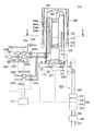
図1を参照すれば、基板処理装置101では、基板の一例となるウエハ200を収納したカセット110が使用されており、ウエハ200は半導体シリコン等の材料から構成されている。基板処理装置101は筐体111を備えており、筐体111の内部にはカセットステージ114が設置されている。カセット110はカセットステージ114上に工程内搬送装置(図示せず)によって搬入されたり、カセットステージ114上から搬出されたりする。
Referring to FIG. 1, a
カセットステージ114上にはカセット110が、工程内搬送装置(図示せず)によって、カセット110内のウエハ200が垂直姿勢を保持しかつカセット110のウエハ出し入れ口が上方向を向くように載置される。カセットステージ114は、カセット110を筐体111の後方に向けて縦方向に90°回転させ、カセット110内のウエハ200を水平姿勢とさせ、カセット110のウエハ出し入れ口を筐体111の後方を向かせるような動作が可能となるよう構成されている。
The cassette 110 is placed on the
筐体111内の前後方向の略中央部にはカセット棚105が設置されており、カセット棚105は複数段複数列にて複数個のカセット110を保管するように構成されている。カセット棚105にはウエハ移載機構125の搬送対象となるカセット110が収納される移載棚123が設けられている。
A
カセットステージ114の上方には予備カセット棚107が設けられ、予備的にカセット110を保管するように構成されている。
A
カセットステージ114とカセット棚105との間には、カセット搬送装置118が設置されている。カセット搬送装置118は、カセット110を保持したまま昇降可能なカセットエレベータ118aと、搬送機構としてのカセット搬送機構118bとを備えている。カセット搬送装置118はカセットエレベータ118aとカセット搬送機構118bとの連動動作により、カセットステージ114とカセット棚105と予備カセット棚107と移載棚123との間で、カセット110を搬送するように構成されている。
A cassette carrying
カセット棚105の後方には、ウエハ移載機構125が設置されている。ウエハ移載機構125は、ウエハ200を水平方向に回転ないし直動可能なウエハ移載装置125aと、ウエハ移載装置125aを昇降させるためのウエハ移載装置エレベータ125bとを備えている。ウエハ移載装置125aにはウエハ200をピックアップし、水平姿勢で保持するためのツイーザ125cが設けられている。ウエハ移載装置125はウエハ移載装置125aとウエハ移載装置エレベータ125bとの連動動作により、ツイーザ125cをウエハ200の載置部として、ウエハ200を移載棚123上のカセット110からボート217に対して装填(チャージング)したり、ボート217から脱装(ディスチャージング)して移載棚123上のカセット110に収容したりするように構成されている。
A
筐体111の後部上方には、ウエハ200を熱処理する処理炉202が設けられており、処理炉202の下端部が炉口シャッタ147により開閉されるように構成されている。
A
処理炉202の下方には処理炉202に対しボート217を昇降させるボートエレベータ115が設けられている。ボートエレベータ115の昇降台にはアーム128が連結されており、アーム128にはシールキャップ219が水平に据え付けられている。シールキャップ219はボート217を垂直に支持するとともに、処理炉202の下端部を閉塞可能なように構成されている。
Below the
ボート217は複数の保持部材を備えており、複数枚(例えば50〜150枚程度)のウエハ200をその中心を揃えて垂直方向に整列させた状態で、それぞれ水平に保持するように構成されている。
The
カセット棚105の上方には、清浄化した雰囲気であるクリーンエアを供給するクリーンユニット134aが設置されている。クリーンユニット134aは供給ファン(図示せず)および防塵フィルタ(図示せず)を備えており、クリーンエアを筐体111の内部に流通させるように構成されている。
Above the
筐体111の左側端部には、クリーンエアを供給するクリーンユニット134bが設置されている。クリーンユニット134bも供給ファン(図示せず)および防塵フィルタ(図示せず)を備えており、クリーンエアをウエハ移載装置125aやボート217等の近傍を流通させるように構成されている。当該クリーンエアは、ウエハ移載装置125aやボート217等の近傍を流通した後に、筐体111の外部に排気されるようになっている。
A
筐体111は、後方に、後側部301、302を備えている。後側部301と後側部302の間は、基板処理装置101のメンテナンスの際に使用されるメンテナンススペース303となっている。
The
続いて、基板処理装置101の主な動作について説明する。
Next, main operations of the
工程内搬送装置(図示略)によってカセット110がカセットステージ114上に搬入されると、カセット110は、ウエハ200がカセットステージ114の上で垂直姿勢を保持し、カセット110のウエハ出し入れ口が上方向を向くようにカセットステージ114上に載置される。その後、カセット110は、カセットステージ114によって、カセット110内のウエハ200が水平姿勢となり、カセット110のウエハ出し入れ口が筐体111の後方を向くように、筐体111の後方に向かって縦方向に90°回転させられる。
When the cassette 110 is loaded onto the
その後、カセット110は、カセット棚105ないし予備カセット棚107の指定された棚位置へカセット搬送装置118によって自動的に搬送され受け渡され、一時的に保管された後、カセット棚105ないし予備カセット棚107からカセット搬送装置118によって移載棚123に移載されるか、もしくは直接移載棚123に搬送される。
Thereafter, the cassette 110 is automatically transported and delivered by the
カセット110が移載棚123に移載されると、ウエハ200はカセット110からウエハ移載装置125aのツイーザ125cによってカセット110のウエハ出し入れ口を通じてピックアップされ、ウエハ移載装置125aとウエハ移載装置エレベータ125bとの連動動作によって、ボート217に装填(チャージング)される。ボート217にウエハ200を受け渡したウエハ移載装置125aはカセット110に戻り、後続のウエハ200をボート217に装填する。
When the cassette 110 is transferred to the
予め指定された枚数のウエハ200がボート217に装填されると、処理炉202の下端部を閉じていた炉口シャッタ147が開き、処理炉202の下端部が開放される。その後、ウエハ200群を保持したボート217がボートエレベータ115の上昇動作により処理炉202内に搬入(ローディング)され、処理炉202の下部がシールキャップ219により閉塞される。
When a predetermined number of
ローディング後は、処理炉202にてウエハ200に対し任意の処理が実施される。その処理後は、上述の逆の手順で、ウエハ200およびカセット110が筐体111の外部に搬出される。
After loading, arbitrary processing is performed on the
次に、図2を参照して、前述した基板処理装置101に使用される処理炉202について説明する。
Next, the
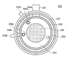
図2を参照すれば、処理炉202にはウエハ200を加熱するための加熱装置(加熱手段)であるヒータ207が設けられている。ヒータ207は上方が閉塞された円筒形状の断熱部材と複数本のヒータ素線とを備えており、断熱部材に対しヒータ素線が設けられたユニット構成を有している。ヒータ207は、保持板としてのヒータベース(図示せず)に支持されることにより垂直に据え付けられている。また、ヒータ207に電力を供給する加熱用電源290が設けられている。ヒータ207の内側には、ヒータ207と同心円状に、ウエハ200を処理するための反応容器(処理容器)を構成する石英製の反応管203が設けられている。
Referring to FIG. 2, the
反応管203の下方には、反応管203の下端開口を気密に閉塞可能な炉口蓋体としてのシールキャップ219が設けられている。シールキャップ219は反応管203の下端に垂直方向下側から当接されるようになっている。シールキャップ219は例えばステンレス等の金属からなり、円盤状に形成されている。反応管203の下部開口端部に設けられた環状のフランジとシールキャップ219の上面との間には気密部材(以下Oリング)220が配置され、両者の間は気密にシールされている。少なくとも、反応管203及びシールキャップ219により処理室201が形成されている。
Below the
シールキャップ219にはボート217を支持するボート支持台218が設けられている。ボート支持台218は、例えば石英や炭化珪素等の耐熱性材料で構成され断熱部として機能すると共にボートを支持する支持体となっている。ボート217は例えば石英や炭化珪素等の耐熱性材料で構成されている。ボート217はボート支持台218に固定された底板210とその上方に配置された天板211とを有しており、底板210と天板211との間に複数本の支柱212が架設された構成を有している(図1参照)。ボート217には複数枚のウエハ200が保持されている。複数枚のウエハ200は、互いに一定の間隔をあけながら水平姿勢を保持した状態で反応管203の管軸方向に多段にかつ互いに中心を揃えた状態で整列した状態で積載配置されボート217の支柱212に支持されている。
The
シールキャップ219の処理室201と反対側にはボートを回転させる回転機構267が設けられている。回転機構267の回転軸255はシールキャップを貫通してボート支持台218に接続されており、基板処理の均一性を向上するために、回転機構267によって、ボート支持台218を介してボート217を回転させることでウエハ200を回転させる。
A
シールキャップ219は反応管203の外部に設けられた昇降機構としてのボートエレベータ115によって垂直方向に昇降され、これによりボート217を処理室201内に対し搬入搬出することが可能となっている。
The
以上の処理炉202では、バッチ処理される複数枚のウエハ200がボート217に対し多段に積層された状態において、ボート217がボート支持台218で支持されながら処理室201に挿入され、ヒータ207が処理室201に挿入されたウエハ200を所定の温度に加熱するようになっている。
In the
処理室201内であって反応管203の下部には、ノズル249aおよびノズル249bが反応管203を貫通するように設けられている。ノズル249aおよびノズル249bにはガス供給管232aおよび232bがそれぞれ接続されている。このように、反応管203には2本のノズル249aおよび249bと、2本のガス供給管232aおよび232bが設けられており、処理室201内へ複数の種類のガスを供給することができるように構成されている。また、後述のように、ガス供給管232aおよびガス供給管232bには、それぞれ不活性ガス供給管232eおよび232f等が接続されている。
A
ガス供給管232aには上流方向から順に、流量制御器(流量制御部)であるマスフローコントローラ(MFC)241a、気化装置(気化手段)であり液体原料を気化して原料ガスとしての気化ガスを生成する気化器271aおよび開閉弁であるバルブ243aが設けられている。バルブ243aを開けることにより、気化器271a内にて生成された気化ガスがノズル249aを介して処理室201内へ供給されるように構成されている。ガス供給管232aには気化器271aとバルブ243aの間に、後述の排気管247に接続されたベントライン232iが接続されている。このベントライン232iには開閉弁であるバルブ243iが設けられており、原料ガスを処理室201に供給しない場合は、バルブ243iを介して原料ガスをベントライン232iへ供給する。バルブ243aを閉め、バルブ243iを開けることにより、気化器271aにおける気化ガスの生成を継続したまま、処理室201内への気化ガスの供給を停止することが可能なように構成されている。気化ガスを安定して生成するには所定の時間を要するが、バルブ243aとバルブ243iの切り替え動作によって、処理室201内への気化ガスの供給・停止をごく短時間で切り替えることが可能なように構成されている。さらにガス供給管232aには、バルブ243aの下流側に不活性ガス供給管232eが接続されている。この不活性ガス供給管232eには、上流方向から順に、流量制御器(流量制御部)であるマスフローコントローラ241eおよび開閉弁であるバルブ243eが設けられている。
In the
ガス供給管232aの先端部には、上述のノズル249aが接続されている。ノズル249aは、反応管203の内壁とウエハ200との間における円弧状の空間に、反応管203の内壁の下部より上部に沿って、ウエハ200の積載方向上方に向かって立ち上がるように設けられている。ノズル249aはL字型のロングのノズルとして構成されている。ノズル249aの側面にはガスを供給するガス供給孔250aが設けられている。ガス供給孔250aは反応管203の中心を向くように開口している。このガス供給孔250aは、反応管203の下部から上部にわたって複数設けられ、それぞれが同一の開口面積を有し、更に同じ開口ピッチで設けられている。
The
主に、ガス供給管232a、ベントライン232i、バルブ243a、243i、気化器271a、マスフローコントローラ241a、ノズル249aにより第1のガス供給系が構成される。また主に、不活性ガス供給管232e、マスフローコントローラ241e、バルブ243eにより第1の不活性ガス供給系が構成される。
A
ガス供給管232bには上流方向から順に、オゾン(O3)ガスを生成する装置であるオゾナイザ500、バルブ243c、流量制御器(流量制御部)であるマスフローコントローラ(MFC)241bおよび開閉弁であるバルブ243bが設けられている。ガス供給管232bの上流側は、酸素(O2)ガスを供給する図示しない酸素ガス供給源に接続されている。オゾナイザ500に供給されたO2ガスは、オゾナイザ500にてO3ガスとなり、処理室201内に供給されるように構成されている。ガス供給管232bにはマスフローコントローラ241bとバルブ243bの間に、後述の排気管247に接続されたベントライン232hが接続されている。このベントライン232hには開閉弁であるバルブ243hが設けられており、O3ガスを処理室201に供給しない場合は、バルブ243hを介して原料ガスをベントライン232hへ供給する。バルブ243bを閉め、バルブ243hを開けることにより、オゾナイザ500によるO3ガスの生成を継続したまま、処理室201内へのO3ガスの供給を停止することが可能なように構成されている。O3ガスを安定して精製するには所定の時間を要するが、バルブ243b、バルブ243hの切り替え動作によって、処理室201内へのO3ガスの供給・停止をごく短時間で切り替えることが可能なように構成されている。さらにガス供給管232bには、バルブ243bの下流側に不活性ガス供給管232fが接続されている。この不活性ガス供給管232fには、上流方向から順に、流量制御器(流量制御部)であるマスフローコントローラ241f、及び開閉弁であるバルブ243fが設けられている。
The
ガス供給管232bの先端部には、上述のノズル249bが接続されている。ノズル249bは、反応管203の内壁とウエハ200との間における円弧状の空間に、反応管203の内壁の下部より上部に沿って、ウエハ200の積載方向上方に向かって立ち上がるように設けられている。ノズル249bはL字型のロングのノズルとして構成されている。ノズル249bの側面にはガスを供給するガス供給孔250bが設けられている。ガス供給孔250bは反応管203の中心を向くように開口している。このガス供給孔250bは、反応管203の下部から上部にわたって複数設けられ、それぞれが同一の開口面積を有し、更に同じ開口ピッチで設けられている。
The
主に、ガス供給管232b、ベントライン232h、オゾナイザ500、バルブ243c、243b、243h、マスフローコントローラ241b、ノズル249bにより第2のガス供給系が構成される。また主に、不活性ガス供給管232f、マスフローコントローラ241f、バルブ243fにより第2の不活性ガス供給系が構成される。
A second gas supply system is mainly configured by the
ガス供給管232aからは、例えば、ジルコニウム原料ガス、すなわちジルコニウム(Zr)を含むガス(ジルコニウム含有ガス)が原料ガスとして、マスフローコントローラ241a、気化器271a、バルブ243a、ノズル249aを介して処理室201内へ供給される。ジルコニウム含有ガスとしては、例えばテトラキスエチルメチルアミノジルコニウム(TEMAZ)を用いることができる。なお、この原料ガスは、常温常圧で固体、液体、及び気体のいずれであっても良いが、ここでは液体として説明する。原料ガスが常温常圧で気体の場合は気化器500を設ける必要はない。
From the
ガス供給管232bには、酸素(O)を含むガス(酸素含有ガス)であって例えばO2ガスが供給され、オゾナイザ500にてO3ガスとなり、酸化ガス(酸化剤)として、バルブ243c、マスフローコントローラ241b、バルブ243b、ノズル249bを介して処理室201内へ供給される。また、オゾナイザ500にてO3ガスを生成せずに酸化ガスとしてO2ガスを処理室201内へ供給することも可能である。
The
不活性ガス供給管232eおよび232fからは、例えば窒素(N2)ガスが、それぞれマスフローコントローラ241eおよび241f、バルブ243eおよび243f、ガス供給管232aおよび232b、ノズル249aおよび249bを介して処理室201内に供給される。
From the inert
反応管203内には温度検出器としての温度センサ263が設置されており、温度センサ263により検出された温度情報に基づきヒータ207への通電具合を調整することで、処理室201内の温度が所望の温度分布となるように構成されている。温度センサ263は、ノズル249aおよび249bと同様にL字型に構成されており、反応管203の内壁に沿って設けられている。
A
反応管203には、処理室201内の雰囲気を排気する排気系300が設けられている。排気系300には、上流側(処理室201側)から順に、排気管231、圧力調整器(圧力調整部)としてのAPC(Auto Pressure Controller)バルブ244、排気管320、排気管330、排気管340、真空排気装置としての真空ポンプ246および排気管247が設けられている。排気管231には、処理室201内の圧力を検出する圧力検出器(圧力検出部)としての圧力センサ245が設けられている。真空ポンプ246の下流側の排気管247は廃ガス処理装置(図示せず)等に接続されている。排気系300は、処理室201内の圧力が所定の圧力(真空度)となるよう真空排気し得るように構成されている。なお、APCバルブ243は、弁を開閉して処理室201内の真空排気・真空排気停止ができ、更に弁開度を調節してコンダクタンスを調整して処理室201内の圧力調整をできるようになっている開閉弁である。
The
制御部(制御手段)であるコントローラ121が、マスフローコントローラ241a、241b、241eおよび241f、バルブ243a、243b、243c、243e、243f、243hおよび243i、気化器271a、オゾナイザ500、圧力センサ245、APCバルブ244、真空ポンプ246、加熱用電源250、温度センサ263、ボート回転機構267、ボートエレベータ115等に接続されている。コントローラ121により、マスフローコントローラ241a、241b、241eおよび241fによる各種ガスの流量調整動作、バルブ243a、243b、243c、243e、243f、243hおよび243iの開閉動作、APCバルブ244の開閉及び圧力センサ245に基づく圧力調整動作、温度センサ263に基づくヒータ207の温度調整動作、気化器271aおよびオゾナイザ500の制御、真空ポンプ246の起動・停止、ボート回転機構267の回転速度調節動作、ボートエレベータ115の昇降動作等の制御等が行われる。
The
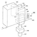
次に、排気系300についてさらに詳細に説明する。上述したように、排気系300には、上流側(処理室201側)から順に、排気管231、APCバルブ244、排気管320、排気管330、排気管340、真空ポンプ246および排気管247が設けられている。図4を参照すれば、排気管231、320、340、247は断面が円形の丸型管である。排気管330は、上流側から順に排気管331〜334を備えている。
Next, the
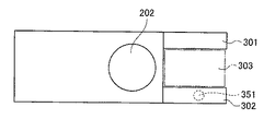
排気管331〜333は、横断面形状が互いに同じであり、上下に積層されている。排気管331〜333は横断面が矩形の角型管である。従って、横断面積を大きくしてコンダクタンスを大きくしても、基板処理装置101の筐体111の後側部302内に収容することができ、基板処理装置101のフットプリントが拡大することはない(図7参照)。これに対して、断面が円状の丸型管360を使用して、コンダクタンスを大きくするため、その横断面積を大きくすると、図8に示すように、丸型管360を収容するために筐体111の後側部302’を大きくする必要が生じ、その分、基板処理装置101のフットプリントが拡大してしまう。排気系300の構成によるが、図9に示すように、筐体111の後側部302内に収容することができる丸型管351と、図7に示すように筐体111の後側部302内に収容することができる角型排気管331〜333との比較では、角型排気管331〜333を使用した場合の方が、N2、30slm供給で、数Pa〜数十Paの低圧化が図れた。このように、角型排気管331〜333を使用することによって、基板処理装置101のフットプリントを増大させることなく、排気系300のコンダクタンスを改善でき、真空ポンプ246の排気性能を生かすことができるようになる。その結果、基板処理装置101のフットプリントを増大させることなく、低圧化をすることができ、微細化に伴うガス吸着特性改善を図ることができるようになる。なお、排気管331〜333の断面積は、排気量(処理室201内の到達圧力)に応じて決定される。
The
このように、本実施の形態では、コンダクタンスを改善でき、排気量を大きくできるため、低圧化を達成できるので、本実施の形態の装置は、蒸気圧の低い原料ガスを用いる装置に好適に使用できる。 As described above, in this embodiment, the conductance can be improved and the displacement can be increased, so that a low pressure can be achieved. Therefore, the apparatus of the present embodiment is preferably used for an apparatus using a raw gas having a low vapor pressure. it can.
また、プラズマ処理を行う装置では低圧化が要求されるので、本実施の形態の装置は、プラズマ処理を行う装置に好適に使用できる。 In addition, since a low pressure is required for an apparatus that performs plasma processing, the apparatus of this embodiment can be suitably used for an apparatus that performs plasma processing.
図5を参照すれば、排気管331〜333は、その縦(A)横(B)比(A/B)が、8:1以下であることが好ましい。装置幅を従来の丸型管を用いた場合と同様に維持しつつ所望の到達圧力を達成するために好適だからである。
Referring to FIG. 5, the
また、図5に示すように、排気管331〜333は、補強のために、それぞれ少なくとも一つのリブ370を有することが好ましい。リブ370は、図5に示すように、排気管331〜333の内側に設けてもよく、図6に示すように、排気管331〜333に外付けしてもよい。
Further, as shown in FIG. 5, the
なお、筐体111は、クリーンルームの床400の上に設置されているので、筐体111の後側部302内に収容されている排気管331〜333も、クリーンルームの床400の上に設置されている。排気管334は、クリーンルームの床400の下に設置されている。排気管334も横断面が矩形の角型排気管であるが、クリーンルームの床400の下に設置されているので、その大きさは、基板処理装置101のフットプリントに直接的には影響を与えない。排気管340および真空ポンプ246もクリーンルームの床400の下に設置されている。排気管247は、屋外等に設置された廃ガス処理装置等にクリーンルームの床400の下を介して接続されている。
Since the
なお、処理炉202と角型の排気管330(排気管331〜333)とを直結させていないのは、セットアップやメンテナンス時に処理炉202を出せないためである。
The reason why the
また、排気管331〜333は、横断面が矩形の角型管であるが、排気管331〜333の横断面は、長方形でもよく、矩形やL字型でもよい。この場合も、補強のために、排気管の内側または外側にリブを有することが好ましい。
The
さらに、排気管331〜333として、断面が楕円形の排気管を用いてもよい。この場合も、補強のために、排気管の内側または外側にリブを有することが好ましい。
Further, as the
このように、排気管331〜333として、排気方向と垂直な方向の断面が、長方形または楕円形状の部分を有する排気管を用いることが好ましく、排気方向と垂直な方向の断面が、長方形または楕円形状の排気管を用いることがより好ましい。この場合も、補強のために、排気管の内側または外側にリブを有することが好ましい。
As described above, as the
次に、上述の基板処理装置の処理炉を用いて半導体装置(半導体デバイス)の製造工程の一工程として、基板上に、DRAM(Dynamic Random Access Memory)のキャパシタに好適に用いられる絶縁膜を成膜するシーケンス例について説明する。尚、以下の説明において、基板処理装置を構成する各部の動作はコントローラ121により制御される。
Next, as a step of the manufacturing process of the semiconductor device (semiconductor device) using the processing furnace of the substrate processing apparatus described above, an insulating film suitable for a DRAM (Dynamic Random Access Memory) capacitor is formed on the substrate. An example of a film forming sequence will be described. In the following description, the operation of each part constituting the substrate processing apparatus is controlled by the
CVD(Chemical Vapor Deposition)法やALD(Atomic Layer Deposition)法では、例えば、CVD法の場合、形成する膜を構成する複数の元素を含む複数種類のガスを同時に供給し、また、ALD法の場合、形成する膜を構成する複数の元素を含む複数種類のガスを交互に供給する。そして、ガス供給時のガス供給流量、ガス供給時間、プラズマパワーなどの供給条件を制御することによりシリコン窒化膜(SiN膜)やシリコン酸化膜(SiO膜)を形成する。それらの技術では、例えばSiN膜を形成する場合、膜の組成比が化学量論組成であるN/Si≒1.33となるように、また例えばSiO膜を形成する場合、膜の組成比が化学量論組成であるO/Si≒2となるようにすることを目的として、供給条件を制御する。 In the CVD (Chemical Vapor Deposition) method and the ALD (Atomic Layer Deposition) method, for example, in the case of the CVD method, a plurality of types of gases including a plurality of elements constituting the film to be formed are supplied at the same time. A plurality of types of gas containing a plurality of elements constituting the film to be formed are alternately supplied. Then, a silicon nitride film (SiN film) or a silicon oxide film (SiO film) is formed by controlling supply conditions such as a gas supply flow rate, a gas supply time, and plasma power at the time of gas supply. In those techniques, for example, when forming a SiN film, the composition ratio of the film is N / Si≈1.33 which is a stoichiometric composition, and when forming a SiO film, for example, the composition ratio of the film is The supply conditions are controlled for the purpose of O / Si≈2, which is the stoichiometric composition.
一方、形成する膜の組成比が化学量論組成とは異なる所定の組成比となるようにすることを目的として、供給条件を制御することも可能である。すなわち、形成する膜を構成する複数の元素のうち少なくとも一つの元素が他の元素よりも化学量論組成に対し過剰となるようにすることを目的として、供給条件を制御する。このように形成する膜を構成する複数の元素の比率、すなわち、膜の組成比を制御しつつ成膜を行うことも可能である。 On the other hand, it is possible to control the supply conditions for the purpose of setting the composition ratio of the film to be formed to a predetermined composition ratio different from the stoichiometric composition. That is, the supply conditions are controlled for the purpose of making at least one element out of the plurality of elements constituting the film to be formed more excessive than the other elements with respect to the stoichiometric composition. It is also possible to perform film formation while controlling the ratio of a plurality of elements constituting the film to be formed as described above, that is, the composition ratio of the film.
以下では、図10、図11を参照して、2種類の元素(ZrとO)を含む2種類のガス(TEMAZガスとO3ガス)を交互に供給して化学量論組成を有する膜(ZrO2膜)を、DRAMのキャパシタ用高誘電率絶縁膜として形成するシーケンス例について説明する。 In the following, referring to FIG. 10 and FIG. 11, a film having a stoichiometric composition by alternately supplying two kinds of gas (TEMAZ gas and O 3 gas) containing two kinds of elements (Zr and O) ( A sequence example of forming a (ZrO 2 film) as a high dielectric constant insulating film for a DRAM capacitor will be described.
ヒータ207を制御して処理室201内を例えば150℃〜250℃の範囲の所定の温度に保持しておく。
The
その後、複数枚のウエハ200がボート217に装填(ウエハチャージ)される(ステップS201)と、複数枚のウエハ200を支持したボート217は、ボートエレベータ115によって持ち上げられて処理室201内に搬入(ボートロード)される(ステップS202)。この状態で、シールキャップ219はOリング220を介して反応管203の下端をシールした状態となる。
Thereafter, when a plurality of
その後、処理室201内が所望の圧力(真空度)となるように真空ポンプ246によって真空排気される。この際、処理室201内の圧力は、圧力センサ245で測定され、この測定された圧力に基づきAPCバルブ244が、フィードバック制御される(ステップS203:圧力調整)。また、処理室201内が所望の温度となるようにヒータ207によって加熱されているが、この際、処理室201内が所望の温度分布となるように、温度センサ263が検出した温度情報に基づきヒータ207への加熱用電源250からの通電具合がフィードバック制御される(ステップS203:温度調整)。続いて、回転機構267により、ボート217が回転されることで、ウエハ200が回転される。
Thereafter, the inside of the
次に、TEMAZガスとO3ガスを処理室201内に供給することにより絶縁膜であるZrO2膜をALD法で成膜するZrO2膜形成工程を行う。ZrO2膜形成工程では次の4つのステップを順次実行する。
Next, the ZrO 2 film forming step of forming an ALD method ZrO 2 film is an insulating film by supplying TEMAZ gas and the O 3 gas into the
<ステップS204>
ステップS204では、まずTEMAZガスを流す。ガス供給管232aのバルブ243aを開き、ベントライン232iのバルブ243iを閉じることで、気化器271aを介してガス供給管232a内にTEMAZガスを流す。ガス供給管232a内を流れたTEMAZガスは、マスフローコントローラ241aにより流量調整される。流量調整されたTEMAZガスはノズル249aのガス供給孔250aから処理室201内に供給されつつガス排気系300から排気される。このとき、同時にバルブ243eを開き、不活性ガス供給管232e内にN2ガス等の不活性ガスを流す。不活性ガス供給管232e内を流れたN2ガスは、マスフローコントローラ241eにより流量調整される。流量調整されたN2ガスはTEMAZガスと一緒に処理室201内に供給されつつガス排気系300から排気される。
<Step S204>
In step S204, first, TEMAZ gas is flowed. By opening the
このとき、APCバルブ244を適正に調整して処理室201内の圧力を、例えば50〜400Paの範囲内の圧力とする。マスフローコントローラ241aで制御するTEMAZガスの供給流量は、例えば0.1〜0.5g/分の範囲内の流量とする。ウエハ200をTEMAZガスに晒す時間、すなわちガス供給時間(照射時間)は、例えば30〜240秒間の範囲内の時間とする。このときヒータ207の温度は、ウエハ200の温度が、例えば150〜250℃の範囲内の温度となるような温度に設定する。
At this time, the
TEMAZガスの供給により、ウエハ200表面上に、ジルコニウムを含む層が形成される。すなわち、ウエハ200上に1原子層未満から数原子層のジルコニウム含有層としてのジルコニウム層(Zr層)が形成される。ジルコニウム含有層はTEMAZの化学吸着(表面吸着)層であってもよい。なお、ジルコニウムは、それ単独で固体となる元素である。ここでジルコニウム層とはジルコニウムにより構成される連続的な層の他、不連続な層やこれらが重なってできる薄膜をも含む。なお、ジルコニウムにより構成される連続的な層を薄膜という場合もある。また、TEMAZの化学吸着層とはTEMAZ分子の連続的な化学吸着層の他、不連続な化学吸着層をも含む。なお、ウエハ200上に形成されるジルコニウム含有層の厚さが数原子層を超えると、後述するステップ206での酸化の作用がジルコニウム含有層の全体に届かなくなる。また、ウエハ200上に形成可能なジルコニウム含有層の最小値は1原子層未満である。よって、ジルコニウム含有層の厚さは1原子層未満から数原子層とするのが好ましい。なお、ウエハ温度及び処理室201内の圧力等の条件を調整することにより、TEMAZガスが自己分解する条件下では、ウエハ200上にジルコニウムが堆積することでジルコニウム層が形成され、TEMAZガスが自己分解しない条件下では、ウエハ200上にTEMAZが化学吸着することでTEMAZガスの化学吸着層が形成されるよう、形成される層を調整することができる。なお、ウエハ200上にTEMAZの化学吸着層を形成する場合と比較して、ウエハ200上にジルコニウム層を形成する方が、成膜レートを高くすることができる。また、ウエハ200上にジルコニウム層を形成する方が、ウエハ200上にTEMAZの化学吸着層を形成する場合と比較して、より緻密な層を形成することができる。
By supplying the TEMAZ gas, a layer containing zirconium is formed on the surface of the
<ステップS205>
ステップS205では、ジルコニウム含有層が形成された後、バルブ243aを閉じ、バルブ243iを開けて処理室内へのTEMAZガスの供給を停止し、TEMAZガスをベントライン232iへ流す。このとき、ガス排気系300のAPCバルブ244は開いたままとして、真空ポンプ246により処理室201内を真空排気し、処理室201内に残留する未反応もしくはジルコニウム含有層形成に寄与した後のTEMAZガスを処理室201内から排除する。なお、この時バルブ243eは開いたままとして、N2ガスの処理室201内への供給を維持する。これにより、処理室201内に残留する未反応もしくはジルコニウム含有層形成に寄与した後のTEMAZガスを処理室201内から排除する効果を高める。不活性ガスとしては、N2ガスの他、Arガス、Heガス、Neガス、Xeガス等の希ガスを用いてもよい。
<Step S205>
In step S205, after the zirconium-containing layer is formed, the
<ステップS206>
ステップS206では、処理室201内の残留ガスを除去した後、ガス供給管232b内にO2ガスを流す。ガス供給管232bを流れたO2ガスは、オゾナイザ500によりO3ガスとなる。ガス供給管232bのバルブ243cおよびバルブ243bを開き、ベントライン232hのバルブ243hを閉めることで、ガス供給管232b内を流れたO3ガスは、マスフローコントローラ241dにより流量調整され、ノズル249bのガス供給孔250bから処理室201内に供給されつつガス排気系300から排気される。この時同時にバルブ243fを開き、不活性ガス供給管232f内にN2ガスを流す。N2ガスはO3ガスと一緒に処理室201内に供給されつつガス排気系300から排気される。
<Step S206>
In step S206, after the residual gas in the
O3ガスを流すときは、APCバルブ244を適正に調整して処理室201内の圧力を、例えば50〜400Paの範囲内の圧力とする。マスフローコントローラ241bで制御するO3ガスの供給流量は、例えば10〜20slmの範囲内の流量とする。O3ガスにウエハ200を晒す時間、すなわちガス供給時間(照射時間)は、例えば60〜300秒間の範囲内の時間とする。このときのヒータ207の温度は、ステップS204と同様、ウエハ200の温度が150〜250℃の範囲内の温度となるような温度に設定する。
When flowing the O 3 gas, the
このとき、処理室201内に流しているガスはO3ガスであり、処理室201内にはTEMAZガスは流していない。したがって、O3ガスは気相反応を起こすことはなく、ステップS204でウエハ200上に形成されたジルコニウム含有層の一部と反応する。これによりジルコニウム含有層は酸化されて、ジルコニウムおよび酸素を含む層、すなわち、ジルコニウム酸化層(ZrO2層)へと改質される。
At this time, the gas flowing into the
<ステップS207>
ステップS207では、ガス供給管232bのバルブ243bを閉じ、バルブ243hを開けて処理室内へのO3ガスの供給を停止し、O3ガスをベントライン232hへ流す。このとき、ガス排気系300のAPCバルブ244は開いたままとして、真空ポンプ246により処理室201内を真空排気し、処理室201内に残留する未反応もしくは酸化に寄与した後のO3ガスを処理室201内から排除する。尚、この時バルブ243fは開いたままとして、N2ガスの処理室201内への供給を維持する。これにより、処理室201内に残留する未反応もしくは酸化に寄与した後のO3ガスを処理室201内から排除する効果を高める。酸素含有ガスとしては、O3ガス以外に、O2ガス等を用いてもよい。
<Step S207>
In step S207, it closes the
上述したステップS204〜S207を1サイクルとして、このサイクルを少なくとも1回以上行う(ステップS208)ことにより、ウエハ200上に所定膜厚のジルコニウムおよび酸素を含む絶縁膜、すなわち、ZrO2膜を成膜することができる。
The above-described steps S204 to S207 are set as one cycle, and this cycle is performed at least once (step S208), whereby an insulating film containing a predetermined thickness of zirconium and oxygen, that is, a ZrO 2 film is formed on the
所定膜厚のZrO2膜を形成する成膜処理がなされると、バルブ243e、バルブ243fを開き、不活性ガス供給管232e、232f内にN2等の不活性ガスを流して、N2等の不活性ガスを処理室201内へ供給しつつ排気することで処理室201内を不活性ガスでパージする(ガスパージ:ステップS210)。その後、処理室201内の雰囲気を不活性ガスで置換し(不活性ガス置換)、処理室201内の圧力を常圧に復帰する(大気圧復帰:ステップS212)。その後、ボートエレベータ115によりシールキャップ219が下降されて、マニホールド209の下端が開口されるとともに、処理済ウエハ200がボート217に支持された状態で反応管203の下端から処理室201の外部に搬出(ボートアンロード:ステップS214)される。その後、処理済ウエハ200はボート217より取出される(ウエハディスチャージ:ステップS216)。
When the film formation process for forming a ZrO 2 film with a predetermined thickness is performed, the
(本発明の好ましい態様)
以下に、本発明の好ましい態様について付記する。
(Preferred embodiment of the present invention)
Hereinafter, preferred embodiments of the present invention will be additionally described.
(付記1)
本発明の好ましい一態様によれば、
複数の基板を積載配置して収容する処理容器と、
前記処理容器に、前記基板を処理する処理ガスを供給する処理ガス供給手段と、
前記処理容器を排気する排気手段と、
を有し、
前記排気手段は、真空ポンプと、前記処理容器と真空ポンプを接続する排気配管とを備え、前記排気配管の少なくとも一部が、リブ構造を有すると共に、排気方向と垂直な方向の断面が、長方形または楕円形状の部分を有する配管で構成される基板処理装置が提供される。
(Appendix 1)
According to a preferred aspect of the present invention,
A processing container for stacking and accommodating a plurality of substrates; and
A processing gas supply means for supplying a processing gas for processing the substrate to the processing container;
Exhaust means for exhausting the processing vessel;
Have
The exhaust means includes a vacuum pump and an exhaust pipe connecting the processing container and the vacuum pump, and at least a part of the exhaust pipe has a rib structure, and a cross section in a direction perpendicular to the exhaust direction is rectangular. Alternatively, a substrate processing apparatus including a pipe having an elliptical portion is provided.
(付記2)
付記1の基板処理装置であって、好ましくは、前記排気配管の前記少なくとも一部が、リブ構造を有すると共に、排気方向と垂直な方向の断面が、長方形または楕円形状の配管で構成される。
(Appendix 2)
The substrate processing apparatus according to appendix 1, wherein the at least part of the exhaust pipe preferably has a rib structure, and a cross section in a direction perpendicular to the exhaust direction is formed of a rectangular or elliptical pipe.
(付記3)
付記1の基板処理装置であって、好ましくは、前記排気配管の前記少なくとも一部が、リブ構造を有すると共に、排気方向と垂直な方向の断面が、長方形の配管で構成される。
(Appendix 3)
The substrate processing apparatus according to appendix 1, wherein at least a part of the exhaust pipe preferably has a rib structure, and a cross section in a direction perpendicular to the exhaust direction is formed of a rectangular pipe.
(付記4)
付記1の基板処理装置であって、好ましくは、前記長方形の断面の縦横比を8:1以下とする。
(Appendix 4)
The substrate processing apparatus according to appendix 1, wherein the aspect ratio of the rectangular cross section is preferably 8: 1 or less.
(付記5)
付記1〜4のいずれか一つの基板処理装置であって、好ましくは、前記処理ガス供給手段は、2種の異なる処理ガスを前記処理容器に交互に供給し、高誘電率膜を形成するよう構成される。
(Appendix 5)
The substrate processing apparatus according to any one of appendices 1 to 4, preferably, the processing gas supply means alternately supplies two different processing gases to the processing container to form a high dielectric constant film. Composed.
以上、本発明の種々の典型的な実施の形態を説明してきたが、本発明はそれらの実施の形態に限定されない。従って、本発明の範囲は、次の特許請求の範囲によってのみ限定されるものである。 While various typical embodiments of the present invention have been described above, the present invention is not limited to these embodiments. Accordingly, the scope of the invention is limited only by the following claims.
101 基板処理装置
115 ボートエレベータ
121 コントローラ
200 ウエハ
201 処理室
202 処理炉
203 反応管
207 ヒータ
217 ボート
218 ボート支持台
219 シールキャップ
231、320、340、247 排気管
244 APCバルブ
245 圧力センサ
246 真空ポンプ
250 加熱用電源
263 温度センサ
267 回転機構
232a、232b ガス供給管
249a、249b ノズル
241a、241b、241e、241f マスフローコントローラ
271a 気化器
232e、232f 不活性ガス供給管
331〜334 角型排気管
DESCRIPTION OF
Claims (5)
前記処理容器を収容する筐体と、
前記基板に対して、処理ガスを供給する処理ガス供給手段と、
前記処理容器を排気する排気手段と、
を有し、
前記排気手段は、
前記処理容器に接続される第1の排気配管と、前記第1の排気配管と真空ポンプとの間に設けられ、前記第1の排気配管に接続する第2の排気配管と、を備え、
前記第1の排気配管は、前記第1の排気配管の排気方向と垂直な方向の断面が円形であり、
前記第2の排気配管は、前記第2の排気配管の排気方向が鉛直方向に延びるように設けられ、前記第2の排気配管の排気方向と垂直な方向の断面が、長方形または楕円形状であり、少なくとも一部がリブ構造を有し、
前記筐体は、水平方向の断面が矩形状である配管収容部を備え、前記第2の排気配管は前記配管収容部に収容されている、
基板処理装置。 A processing container for containing a substrate;
A housing for accommodating the processing container;
To the substrate, a processing gas supply unit for supplying a processing gas,
Exhaust means for exhausting the processing vessel;
Have
The exhaust means includes
A first exhaust pipe connected to the processing container; and a second exhaust pipe provided between the first exhaust pipe and the vacuum pump and connected to the first exhaust pipe.
The first exhaust pipe has a circular cross section in a direction perpendicular to the exhaust direction of the first exhaust pipe,
The second exhaust pipe is provided such that an exhaust direction of the second exhaust pipe extends in a vertical direction, and a cross section in a direction perpendicular to the exhaust direction of the second exhaust pipe is rectangular or elliptical . , At least a portion has a rib structure,
The housing includes a pipe housing portion having a rectangular cross section in the horizontal direction, and the second exhaust pipe is housed in the pipe housing portion.
Substrate processing equipment.
前記第3の排気配管は、
前記第3の排気配管の排気方向と垂直な方向の断面積が前記第2の排気配管の断面積より大きく、
前記配管収容部の外部に設けられる、請求項1又は2に記載の基板処理装置。 A third exhaust pipe provided between the second exhaust pipe and the vacuum pump;
The third exhaust pipe is
The cross-sectional area of the third exhaust pipe in the direction perpendicular to the exhaust direction is larger than the cross-sectional area of the second exhaust pipe;
The substrate processing apparatus of Claim 1 or 2 provided in the exterior of the said piping accommodating part.
前記処理容器に接続される第1の排気配管、及び前記第1の排気配管と真空ポンプとの間に設けられ、前記第1の排気配管に接続する第2の排気配管から前記処理ガスを排気する工程と、
を行う工程を有し、
前記第1の排気配管は、前記第1の排気配管の排気方向と垂直な方向の断面が円形であり、
前記第2の排気配管は、前記第2の排気配管の排気方向が鉛直方向に延びるように設けられ、前記第2の排気配管の排気方向と垂直な方向の断面が長方形または楕円形状であり、少なくとも一部がリブ構造を有し、
前記処理容器を収容する筐体は、水平方向の断面が矩形状である配管収容部を備え、前記第2の排気配管は前記配管収容部に収容されている、
半導体装置の製造方法。 Supplying a processing gas to the substrate accommodated in the processing container;
The processing chamber connected to Ru first exhaust pipe, and exhaust the disposed between the first exhaust pipe and a vacuum pump, the process gas from the second exhaust pipe connected to the first exhaust pipe And a process of
It has a step of performing,
The first exhaust pipe has a circular cross section in a direction perpendicular to the exhaust direction of the first exhaust pipe,
The second exhaust pipe is provided such that an exhaust direction of the second exhaust pipe extends in a vertical direction, and a cross section in a direction perpendicular to the exhaust direction of the second exhaust pipe is rectangular or elliptical, At least a portion has a rib structure,
The housing that houses the processing container includes a pipe housing portion that has a rectangular cross section in the horizontal direction, and the second exhaust pipe is housed in the pipe housing portion.
A method for manufacturing a semiconductor device.
Priority Applications (4)
| Application Number | Priority Date | Filing Date | Title |
|---|---|---|---|
| JP2011260937A JP5921168B2 (en) | 2011-11-29 | 2011-11-29 | Substrate processing equipment |
| KR1020120135133A KR101403982B1 (en) | 2011-11-29 | 2012-11-27 | Exhaust unit, substrate processing apparatus, and method of manufacturing semiconductor device |
| US13/687,709 US20130137279A1 (en) | 2011-11-29 | 2012-11-28 | Exhaust Unit, Substrate Processing Apparatus, and Method of Manufacturing Semiconductor Device |
| US14/622,126 US9646821B2 (en) | 2011-11-29 | 2015-02-13 | Method of manufacturing semiconductor device |
Applications Claiming Priority (1)
| Application Number | Priority Date | Filing Date | Title |
|---|---|---|---|
| JP2011260937A JP5921168B2 (en) | 2011-11-29 | 2011-11-29 | Substrate processing equipment |
Publications (3)
| Publication Number | Publication Date |
|---|---|
| JP2013115275A JP2013115275A (en) | 2013-06-10 |
| JP2013115275A5 JP2013115275A5 (en) | 2014-11-13 |
| JP5921168B2 true JP5921168B2 (en) | 2016-05-24 |
Family
ID=48467280
Family Applications (1)
| Application Number | Title | Priority Date | Filing Date |
|---|---|---|---|
| JP2011260937A Active JP5921168B2 (en) | 2011-11-29 | 2011-11-29 | Substrate processing equipment |
Country Status (3)
| Country | Link |
|---|---|
| US (2) | US20130137279A1 (en) |
| JP (1) | JP5921168B2 (en) |
| KR (1) | KR101403982B1 (en) |
Families Citing this family (246)
| Publication number | Priority date | Publication date | Assignee | Title |
|---|---|---|---|---|
| US9394608B2 (en) | 2009-04-06 | 2016-07-19 | Asm America, Inc. | Semiconductor processing reactor and components thereof |
| US8802201B2 (en) | 2009-08-14 | 2014-08-12 | Asm America, Inc. | Systems and methods for thin-film deposition of metal oxides using excited nitrogen-oxygen species |
| US20130023129A1 (en) | 2011-07-20 | 2013-01-24 | Asm America, Inc. | Pressure transmitter for a semiconductor processing environment |
| US9017481B1 (en) | 2011-10-28 | 2015-04-28 | Asm America, Inc. | Process feed management for semiconductor substrate processing |
| JP6061545B2 (en) * | 2012-08-10 | 2017-01-18 | 株式会社日立国際電気 | Semiconductor device manufacturing method, substrate processing method, and substrate processing apparatus |
| US10714315B2 (en) | 2012-10-12 | 2020-07-14 | Asm Ip Holdings B.V. | Semiconductor reaction chamber showerhead |
| US20160376700A1 (en) | 2013-02-01 | 2016-12-29 | Asm Ip Holding B.V. | System for treatment of deposition reactor |
| US11015245B2 (en) | 2014-03-19 | 2021-05-25 | Asm Ip Holding B.V. | Gas-phase reactor and system having exhaust plenum and components thereof |
| US10858737B2 (en) | 2014-07-28 | 2020-12-08 | Asm Ip Holding B.V. | Showerhead assembly and components thereof |
| US9890456B2 (en) | 2014-08-21 | 2018-02-13 | Asm Ip Holding B.V. | Method and system for in situ formation of gas-phase compounds |
| US10941490B2 (en) | 2014-10-07 | 2021-03-09 | Asm Ip Holding B.V. | Multiple temperature range susceptor, assembly, reactor and system including the susceptor, and methods of using the same |
| US10276355B2 (en) | 2015-03-12 | 2019-04-30 | Asm Ip Holding B.V. | Multi-zone reactor, system including the reactor, and method of using the same |
| US10458018B2 (en) | 2015-06-26 | 2019-10-29 | Asm Ip Holding B.V. | Structures including metal carbide material, devices including the structures, and methods of forming same |
| WO2017047686A1 (en) * | 2015-09-17 | 2017-03-23 | 株式会社日立国際電気 | Gas supply part, substrate processing device and semiconductor device manufacturing method |
| US10211308B2 (en) | 2015-10-21 | 2019-02-19 | Asm Ip Holding B.V. | NbMC layers |
| US11139308B2 (en) | 2015-12-29 | 2021-10-05 | Asm Ip Holding B.V. | Atomic layer deposition of III-V compounds to form V-NAND devices |
| US10529554B2 (en) | 2016-02-19 | 2020-01-07 | Asm Ip Holding B.V. | Method for forming silicon nitride film selectively on sidewalls or flat surfaces of trenches |
| US10865475B2 (en) | 2016-04-21 | 2020-12-15 | Asm Ip Holding B.V. | Deposition of metal borides and silicides |
| US10190213B2 (en) | 2016-04-21 | 2019-01-29 | Asm Ip Holding B.V. | Deposition of metal borides |
| US10367080B2 (en) | 2016-05-02 | 2019-07-30 | Asm Ip Holding B.V. | Method of forming a germanium oxynitride film |
| US11453943B2 (en) | 2016-05-25 | 2022-09-27 | Asm Ip Holding B.V. | Method for forming carbon-containing silicon/metal oxide or nitride film by ALD using silicon precursor and hydrocarbon precursor |
| JP6891252B2 (en) * | 2016-06-30 | 2021-06-18 | 株式会社Kokusai Electric | Substrate processing equipment, semiconductor device manufacturing methods, programs and recording media |
| CN109075020B (en) * | 2016-06-30 | 2024-03-05 | 株式会社国际电气 | Substrate processing apparatus, method for manufacturing semiconductor device, and recording medium |
| US10612137B2 (en) | 2016-07-08 | 2020-04-07 | Asm Ip Holdings B.V. | Organic reactants for atomic layer deposition |
| US9859151B1 (en) | 2016-07-08 | 2018-01-02 | Asm Ip Holding B.V. | Selective film deposition method to form air gaps |
| US9812320B1 (en) | 2016-07-28 | 2017-11-07 | Asm Ip Holding B.V. | Method and apparatus for filling a gap |
| KR102532607B1 (en) | 2016-07-28 | 2023-05-15 | 에이에스엠 아이피 홀딩 비.브이. | Substrate processing apparatus and method of operating the same |
| US9887082B1 (en) | 2016-07-28 | 2018-02-06 | Asm Ip Holding B.V. | Method and apparatus for filling a gap |
| US10643826B2 (en) | 2016-10-26 | 2020-05-05 | Asm Ip Holdings B.V. | Methods for thermally calibrating reaction chambers |
| US11532757B2 (en) | 2016-10-27 | 2022-12-20 | Asm Ip Holding B.V. | Deposition of charge trapping layers |
| US10714350B2 (en) | 2016-11-01 | 2020-07-14 | ASM IP Holdings, B.V. | Methods for forming a transition metal niobium nitride film on a substrate by atomic layer deposition and related semiconductor device structures |
| US10229833B2 (en) | 2016-11-01 | 2019-03-12 | Asm Ip Holding B.V. | Methods for forming a transition metal nitride film on a substrate by atomic layer deposition and related semiconductor device structures |
| KR102546317B1 (en) | 2016-11-15 | 2023-06-21 | 에이에스엠 아이피 홀딩 비.브이. | Gas supply unit and substrate processing apparatus including the same |
| KR20180068582A (en) | 2016-12-14 | 2018-06-22 | 에이에스엠 아이피 홀딩 비.브이. | Substrate processing apparatus |
| US11581186B2 (en) | 2016-12-15 | 2023-02-14 | Asm Ip Holding B.V. | Sequential infiltration synthesis apparatus |
| US11447861B2 (en) | 2016-12-15 | 2022-09-20 | Asm Ip Holding B.V. | Sequential infiltration synthesis apparatus and a method of forming a patterned structure |
| KR20180070971A (en) | 2016-12-19 | 2018-06-27 | 에이에스엠 아이피 홀딩 비.브이. | Substrate processing apparatus |
| US10269558B2 (en) | 2016-12-22 | 2019-04-23 | Asm Ip Holding B.V. | Method of forming a structure on a substrate |
| US10867788B2 (en) | 2016-12-28 | 2020-12-15 | Asm Ip Holding B.V. | Method of forming a structure on a substrate |
| US11390950B2 (en) | 2017-01-10 | 2022-07-19 | Asm Ip Holding B.V. | Reactor system and method to reduce residue buildup during a film deposition process |
| US10468261B2 (en) | 2017-02-15 | 2019-11-05 | Asm Ip Holding B.V. | Methods for forming a metallic film on a substrate by cyclical deposition and related semiconductor device structures |
| US10529563B2 (en) | 2017-03-29 | 2020-01-07 | Asm Ip Holdings B.V. | Method for forming doped metal oxide films on a substrate by cyclical deposition and related semiconductor device structures |
| KR102457289B1 (en) | 2017-04-25 | 2022-10-21 | 에이에스엠 아이피 홀딩 비.브이. | Method for depositing a thin film and manufacturing a semiconductor device |
| US10892156B2 (en) | 2017-05-08 | 2021-01-12 | Asm Ip Holding B.V. | Methods for forming a silicon nitride film on a substrate and related semiconductor device structures |
| US10770286B2 (en) | 2017-05-08 | 2020-09-08 | Asm Ip Holdings B.V. | Methods for selectively forming a silicon nitride film on a substrate and related semiconductor device structures |
| US10886123B2 (en) | 2017-06-02 | 2021-01-05 | Asm Ip Holding B.V. | Methods for forming low temperature semiconductor layers and related semiconductor device structures |
| JP6811146B2 (en) * | 2017-06-23 | 2021-01-13 | 東京エレクトロン株式会社 | How to inspect the gas supply system |
| JP6811147B2 (en) * | 2017-06-23 | 2021-01-13 | 東京エレクトロン株式会社 | How to inspect the gas supply system |
| US11306395B2 (en) | 2017-06-28 | 2022-04-19 | Asm Ip Holding B.V. | Methods for depositing a transition metal nitride film on a substrate by atomic layer deposition and related deposition apparatus |
| KR20190009245A (en) | 2017-07-18 | 2019-01-28 | 에이에스엠 아이피 홀딩 비.브이. | Methods for forming a semiconductor device structure and related semiconductor device structures |
| US11374112B2 (en) | 2017-07-19 | 2022-06-28 | Asm Ip Holding B.V. | Method for depositing a group IV semiconductor and related semiconductor device structures |
| US11018002B2 (en) | 2017-07-19 | 2021-05-25 | Asm Ip Holding B.V. | Method for selectively depositing a Group IV semiconductor and related semiconductor device structures |
| US10541333B2 (en) | 2017-07-19 | 2020-01-21 | Asm Ip Holding B.V. | Method for depositing a group IV semiconductor and related semiconductor device structures |
| US10590535B2 (en) | 2017-07-26 | 2020-03-17 | Asm Ip Holdings B.V. | Chemical treatment, deposition and/or infiltration apparatus and method for using the same |
| US10692741B2 (en) | 2017-08-08 | 2020-06-23 | Asm Ip Holdings B.V. | Radiation shield |
| US10770336B2 (en) | 2017-08-08 | 2020-09-08 | Asm Ip Holding B.V. | Substrate lift mechanism and reactor including same |
| US11769682B2 (en) | 2017-08-09 | 2023-09-26 | Asm Ip Holding B.V. | Storage apparatus for storing cassettes for substrates and processing apparatus equipped therewith |
| US11139191B2 (en) | 2017-08-09 | 2021-10-05 | Asm Ip Holding B.V. | Storage apparatus for storing cassettes for substrates and processing apparatus equipped therewith |
| US11830730B2 (en) | 2017-08-29 | 2023-11-28 | Asm Ip Holding B.V. | Layer forming method and apparatus |
| US11056344B2 (en) | 2017-08-30 | 2021-07-06 | Asm Ip Holding B.V. | Layer forming method |
| KR102491945B1 (en) | 2017-08-30 | 2023-01-26 | 에이에스엠 아이피 홀딩 비.브이. | Substrate processing apparatus |
| US11295980B2 (en) | 2017-08-30 | 2022-04-05 | Asm Ip Holding B.V. | Methods for depositing a molybdenum metal film over a dielectric surface of a substrate by a cyclical deposition process and related semiconductor device structures |
| KR102630301B1 (en) | 2017-09-21 | 2024-01-29 | 에이에스엠 아이피 홀딩 비.브이. | Method of sequential infiltration synthesis treatment of infiltrateable material and structures and devices formed using same |
| US10844484B2 (en) | 2017-09-22 | 2020-11-24 | Asm Ip Holding B.V. | Apparatus for dispensing a vapor phase reactant to a reaction chamber and related methods |
| US10658205B2 (en) | 2017-09-28 | 2020-05-19 | Asm Ip Holdings B.V. | Chemical dispensing apparatus and methods for dispensing a chemical to a reaction chamber |
| US10403504B2 (en) | 2017-10-05 | 2019-09-03 | Asm Ip Holding B.V. | Method for selectively depositing a metallic film on a substrate |
| US10923344B2 (en) | 2017-10-30 | 2021-02-16 | Asm Ip Holding B.V. | Methods for forming a semiconductor structure and related semiconductor structures |
| US10910262B2 (en) | 2017-11-16 | 2021-02-02 | Asm Ip Holding B.V. | Method of selectively depositing a capping layer structure on a semiconductor device structure |
| US11022879B2 (en) | 2017-11-24 | 2021-06-01 | Asm Ip Holding B.V. | Method of forming an enhanced unexposed photoresist layer |
| KR102597978B1 (en) | 2017-11-27 | 2023-11-06 | 에이에스엠 아이피 홀딩 비.브이. | Storage device for storing wafer cassettes for use with batch furnaces |
| US11639811B2 (en) | 2017-11-27 | 2023-05-02 | Asm Ip Holding B.V. | Apparatus including a clean mini environment |
| US10872771B2 (en) | 2018-01-16 | 2020-12-22 | Asm Ip Holding B. V. | Method for depositing a material film on a substrate within a reaction chamber by a cyclical deposition process and related device structures |
| TW202325889A (en) | 2018-01-19 | 2023-07-01 | 荷蘭商Asm 智慧財產控股公司 | Deposition method |
| US11482412B2 (en) | 2018-01-19 | 2022-10-25 | Asm Ip Holding B.V. | Method for depositing a gap-fill layer by plasma-assisted deposition |
| US11018047B2 (en) | 2018-01-25 | 2021-05-25 | Asm Ip Holding B.V. | Hybrid lift pin |
| USD880437S1 (en) | 2018-02-01 | 2020-04-07 | Asm Ip Holding B.V. | Gas supply plate for semiconductor manufacturing apparatus |
| US11081345B2 (en) | 2018-02-06 | 2021-08-03 | Asm Ip Holding B.V. | Method of post-deposition treatment for silicon oxide film |
| WO2019158960A1 (en) | 2018-02-14 | 2019-08-22 | Asm Ip Holding B.V. | A method for depositing a ruthenium-containing film on a substrate by a cyclical deposition process |
| US10896820B2 (en) | 2018-02-14 | 2021-01-19 | Asm Ip Holding B.V. | Method for depositing a ruthenium-containing film on a substrate by a cyclical deposition process |
| KR102636427B1 (en) | 2018-02-20 | 2024-02-13 | 에이에스엠 아이피 홀딩 비.브이. | Substrate processing method and apparatus |
| US10975470B2 (en) | 2018-02-23 | 2021-04-13 | Asm Ip Holding B.V. | Apparatus for detecting or monitoring for a chemical precursor in a high temperature environment |
| US11473195B2 (en) | 2018-03-01 | 2022-10-18 | Asm Ip Holding B.V. | Semiconductor processing apparatus and a method for processing a substrate |
| US11629406B2 (en) | 2018-03-09 | 2023-04-18 | Asm Ip Holding B.V. | Semiconductor processing apparatus comprising one or more pyrometers for measuring a temperature of a substrate during transfer of the substrate |
| US11114283B2 (en) | 2018-03-16 | 2021-09-07 | Asm Ip Holding B.V. | Reactor, system including the reactor, and methods of manufacturing and using same |
| KR102646467B1 (en) | 2018-03-27 | 2024-03-11 | 에이에스엠 아이피 홀딩 비.브이. | Method of forming an electrode on a substrate and a semiconductor device structure including an electrode |
| US11230766B2 (en) | 2018-03-29 | 2022-01-25 | Asm Ip Holding B.V. | Substrate processing apparatus and method |
| US11088002B2 (en) | 2018-03-29 | 2021-08-10 | Asm Ip Holding B.V. | Substrate rack and a substrate processing system and method |
| KR102501472B1 (en) | 2018-03-30 | 2023-02-20 | 에이에스엠 아이피 홀딩 비.브이. | Substrate processing method |
| TWI811348B (en) | 2018-05-08 | 2023-08-11 | 荷蘭商Asm 智慧財產控股公司 | Methods for depositing an oxide film on a substrate by a cyclical deposition process and related device structures |
| TWI816783B (en) | 2018-05-11 | 2023-10-01 | 荷蘭商Asm 智慧財產控股公司 | Methods for forming a doped metal carbide film on a substrate and related semiconductor device structures |
| KR102596988B1 (en) | 2018-05-28 | 2023-10-31 | 에이에스엠 아이피 홀딩 비.브이. | Method of processing a substrate and a device manufactured by the same |
| US11718913B2 (en) | 2018-06-04 | 2023-08-08 | Asm Ip Holding B.V. | Gas distribution system and reactor system including same |
| US11270899B2 (en) | 2018-06-04 | 2022-03-08 | Asm Ip Holding B.V. | Wafer handling chamber with moisture reduction |
| US11286562B2 (en) | 2018-06-08 | 2022-03-29 | Asm Ip Holding B.V. | Gas-phase chemical reactor and method of using same |
| US10797133B2 (en) | 2018-06-21 | 2020-10-06 | Asm Ip Holding B.V. | Method for depositing a phosphorus doped silicon arsenide film and related semiconductor device structures |
| KR102568797B1 (en) | 2018-06-21 | 2023-08-21 | 에이에스엠 아이피 홀딩 비.브이. | Substrate processing system |
| JP2021529254A (en) | 2018-06-27 | 2021-10-28 | エーエスエム・アイピー・ホールディング・ベー・フェー | Periodic deposition methods for forming metal-containing materials and films and structures containing metal-containing materials |
| CN112292477A (en) | 2018-06-27 | 2021-01-29 | Asm Ip私人控股有限公司 | Cyclic deposition methods for forming metal-containing materials and films and structures containing metal-containing materials |
| KR20200002519A (en) | 2018-06-29 | 2020-01-08 | 에이에스엠 아이피 홀딩 비.브이. | Method for depositing a thin film and manufacturing a semiconductor device |
| US10612136B2 (en) | 2018-06-29 | 2020-04-07 | ASM IP Holding, B.V. | Temperature-controlled flange and reactor system including same |
| US10388513B1 (en) | 2018-07-03 | 2019-08-20 | Asm Ip Holding B.V. | Method for depositing silicon-free carbon-containing film as gap-fill layer by pulse plasma-assisted deposition |
| US10755922B2 (en) | 2018-07-03 | 2020-08-25 | Asm Ip Holding B.V. | Method for depositing silicon-free carbon-containing film as gap-fill layer by pulse plasma-assisted deposition |
| US10767789B2 (en) | 2018-07-16 | 2020-09-08 | Asm Ip Holding B.V. | Diaphragm valves, valve components, and methods for forming valve components |
| US11053591B2 (en) | 2018-08-06 | 2021-07-06 | Asm Ip Holding B.V. | Multi-port gas injection system and reactor system including same |
| US10883175B2 (en) | 2018-08-09 | 2021-01-05 | Asm Ip Holding B.V. | Vertical furnace for processing substrates and a liner for use therein |
| US10829852B2 (en) | 2018-08-16 | 2020-11-10 | Asm Ip Holding B.V. | Gas distribution device for a wafer processing apparatus |
| US11430674B2 (en) | 2018-08-22 | 2022-08-30 | Asm Ip Holding B.V. | Sensor array, apparatus for dispensing a vapor phase reactant to a reaction chamber and related methods |
| US11024523B2 (en) | 2018-09-11 | 2021-06-01 | Asm Ip Holding B.V. | Substrate processing apparatus and method |
| KR20200030162A (en) | 2018-09-11 | 2020-03-20 | 에이에스엠 아이피 홀딩 비.브이. | Method for deposition of a thin film |
| US11049751B2 (en) | 2018-09-14 | 2021-06-29 | Asm Ip Holding B.V. | Cassette supply system to store and handle cassettes and processing apparatus equipped therewith |
| CN110970344A (en) | 2018-10-01 | 2020-04-07 | Asm Ip控股有限公司 | Substrate holding apparatus, system including the same, and method of using the same |
| US11232963B2 (en) | 2018-10-03 | 2022-01-25 | Asm Ip Holding B.V. | Substrate processing apparatus and method |
| KR102592699B1 (en) | 2018-10-08 | 2023-10-23 | 에이에스엠 아이피 홀딩 비.브이. | Substrate support unit and apparatuses for depositing thin film and processing the substrate including the same |
| KR102605121B1 (en) | 2018-10-19 | 2023-11-23 | 에이에스엠 아이피 홀딩 비.브이. | Substrate processing apparatus and substrate processing method |
| KR102546322B1 (en) | 2018-10-19 | 2023-06-21 | 에이에스엠 아이피 홀딩 비.브이. | Substrate processing apparatus and substrate processing method |
| USD948463S1 (en) | 2018-10-24 | 2022-04-12 | Asm Ip Holding B.V. | Susceptor for semiconductor substrate supporting apparatus |
| US11087997B2 (en) | 2018-10-31 | 2021-08-10 | Asm Ip Holding B.V. | Substrate processing apparatus for processing substrates |
| KR20200051105A (en) | 2018-11-02 | 2020-05-13 | 에이에스엠 아이피 홀딩 비.브이. | Substrate support unit and substrate processing apparatus including the same |
| US11572620B2 (en) | 2018-11-06 | 2023-02-07 | Asm Ip Holding B.V. | Methods for selectively depositing an amorphous silicon film on a substrate |
| US11031242B2 (en) | 2018-11-07 | 2021-06-08 | Asm Ip Holding B.V. | Methods for depositing a boron doped silicon germanium film |
| US10847366B2 (en) | 2018-11-16 | 2020-11-24 | Asm Ip Holding B.V. | Methods for depositing a transition metal chalcogenide film on a substrate by a cyclical deposition process |
| US10818758B2 (en) | 2018-11-16 | 2020-10-27 | Asm Ip Holding B.V. | Methods for forming a metal silicate film on a substrate in a reaction chamber and related semiconductor device structures |
| US11217444B2 (en) | 2018-11-30 | 2022-01-04 | Asm Ip Holding B.V. | Method for forming an ultraviolet radiation responsive metal oxide-containing film |
| KR102636428B1 (en) | 2018-12-04 | 2024-02-13 | 에이에스엠 아이피 홀딩 비.브이. | A method for cleaning a substrate processing apparatus |
| US11158513B2 (en) | 2018-12-13 | 2021-10-26 | Asm Ip Holding B.V. | Methods for forming a rhenium-containing film on a substrate by a cyclical deposition process and related semiconductor device structures |
| JP2020096183A (en) | 2018-12-14 | 2020-06-18 | エーエスエム・アイピー・ホールディング・ベー・フェー | Method of forming device structure using selective deposition of gallium nitride, and system for the same |
| TWI819180B (en) | 2019-01-17 | 2023-10-21 | 荷蘭商Asm 智慧財產控股公司 | Methods of forming a transition metal containing film on a substrate by a cyclical deposition process |
| KR20200091543A (en) | 2019-01-22 | 2020-07-31 | 에이에스엠 아이피 홀딩 비.브이. | Semiconductor processing device |
| CN111524788B (en) | 2019-02-01 | 2023-11-24 | Asm Ip私人控股有限公司 | Method for topologically selective film formation of silicon oxide |
| KR102638425B1 (en) | 2019-02-20 | 2024-02-21 | 에이에스엠 아이피 홀딩 비.브이. | Method and apparatus for filling a recess formed within a substrate surface |
| KR102626263B1 (en) | 2019-02-20 | 2024-01-16 | 에이에스엠 아이피 홀딩 비.브이. | Cyclical deposition method including treatment step and apparatus for same |
| US11482533B2 (en) | 2019-02-20 | 2022-10-25 | Asm Ip Holding B.V. | Apparatus and methods for plug fill deposition in 3-D NAND applications |
| JP2020136677A (en) | 2019-02-20 | 2020-08-31 | エーエスエム・アイピー・ホールディング・ベー・フェー | Periodic accumulation method for filing concave part formed inside front surface of base material, and device |
| JP2020133004A (en) | 2019-02-22 | 2020-08-31 | エーエスエム・アイピー・ホールディング・ベー・フェー | Base material processing apparatus and method for processing base material |
| US11742198B2 (en) | 2019-03-08 | 2023-08-29 | Asm Ip Holding B.V. | Structure including SiOCN layer and method of forming same |
| KR20200108242A (en) | 2019-03-08 | 2020-09-17 | 에이에스엠 아이피 홀딩 비.브이. | Method for Selective Deposition of Silicon Nitride Layer and Structure Including Selectively-Deposited Silicon Nitride Layer |
| KR20200108243A (en) | 2019-03-08 | 2020-09-17 | 에이에스엠 아이피 홀딩 비.브이. | Structure Including SiOC Layer and Method of Forming Same |
| JP6625256B2 (en) * | 2019-03-27 | 2019-12-25 | 株式会社Kokusai Electric | Substrate processing apparatus, semiconductor device manufacturing method, and recording medium |
| JP6591710B2 (en) * | 2019-03-27 | 2019-10-16 | 株式会社Kokusai Electric | Substrate processing apparatus, semiconductor device manufacturing method, and recording medium |
| JP6591711B2 (en) * | 2019-03-27 | 2019-10-16 | 株式会社Kokusai Electric | Substrate processing apparatus, semiconductor device manufacturing method, and recording medium |
| JP6616917B2 (en) * | 2019-03-27 | 2019-12-04 | 株式会社Kokusai Electric | Substrate processing apparatus, semiconductor device manufacturing method, and recording medium |
| JP6591712B2 (en) * | 2019-03-27 | 2019-10-16 | 株式会社Kokusai Electric | Substrate processing apparatus, semiconductor device manufacturing method, and recording medium |
| JP2020167398A (en) | 2019-03-28 | 2020-10-08 | エーエスエム・アイピー・ホールディング・ベー・フェー | Door opener and substrate processing apparatus provided therewith |
| KR20200116855A (en) | 2019-04-01 | 2020-10-13 | 에이에스엠 아이피 홀딩 비.브이. | Method of manufacturing semiconductor device |
| US11447864B2 (en) | 2019-04-19 | 2022-09-20 | Asm Ip Holding B.V. | Layer forming method and apparatus |
| KR20200125453A (en) | 2019-04-24 | 2020-11-04 | 에이에스엠 아이피 홀딩 비.브이. | Gas-phase reactor system and method of using same |
| KR20200130118A (en) | 2019-05-07 | 2020-11-18 | 에이에스엠 아이피 홀딩 비.브이. | Method for Reforming Amorphous Carbon Polymer Film |
| KR20200130121A (en) | 2019-05-07 | 2020-11-18 | 에이에스엠 아이피 홀딩 비.브이. | Chemical source vessel with dip tube |
| KR20200130652A (en) | 2019-05-10 | 2020-11-19 | 에이에스엠 아이피 홀딩 비.브이. | Method of depositing material onto a surface and structure formed according to the method |
| JP2020188255A (en) | 2019-05-16 | 2020-11-19 | エーエスエム アイピー ホールディング ビー.ブイ. | Wafer boat handling device, vertical batch furnace, and method |
| USD947913S1 (en) | 2019-05-17 | 2022-04-05 | Asm Ip Holding B.V. | Susceptor shaft |
| USD975665S1 (en) | 2019-05-17 | 2023-01-17 | Asm Ip Holding B.V. | Susceptor shaft |
| USD935572S1 (en) | 2019-05-24 | 2021-11-09 | Asm Ip Holding B.V. | Gas channel plate |
| USD922229S1 (en) | 2019-06-05 | 2021-06-15 | Asm Ip Holding B.V. | Device for controlling a temperature of a gas supply unit |
| KR20200141002A (en) | 2019-06-06 | 2020-12-17 | 에이에스엠 아이피 홀딩 비.브이. | Method of using a gas-phase reactor system including analyzing exhausted gas |
| KR20200143254A (en) | 2019-06-11 | 2020-12-23 | 에이에스엠 아이피 홀딩 비.브이. | Method of forming an electronic structure using an reforming gas, system for performing the method, and structure formed using the method |
| USD944946S1 (en) | 2019-06-14 | 2022-03-01 | Asm Ip Holding B.V. | Shower plate |
| USD931978S1 (en) | 2019-06-27 | 2021-09-28 | Asm Ip Holding B.V. | Showerhead vacuum transport |
| KR20210005515A (en) | 2019-07-03 | 2021-01-14 | 에이에스엠 아이피 홀딩 비.브이. | Temperature control assembly for substrate processing apparatus and method of using same |
| JP2021015791A (en) | 2019-07-09 | 2021-02-12 | エーエスエム アイピー ホールディング ビー.ブイ. | Plasma device and substrate processing method using coaxial waveguide |
| CN112216646A (en) | 2019-07-10 | 2021-01-12 | Asm Ip私人控股有限公司 | Substrate supporting assembly and substrate processing device comprising same |
| KR20210010307A (en) | 2019-07-16 | 2021-01-27 | 에이에스엠 아이피 홀딩 비.브이. | Substrate processing apparatus |
| KR20210010816A (en) | 2019-07-17 | 2021-01-28 | 에이에스엠 아이피 홀딩 비.브이. | Radical assist ignition plasma system and method |
| KR20210010820A (en) | 2019-07-17 | 2021-01-28 | 에이에스엠 아이피 홀딩 비.브이. | Methods of forming silicon germanium structures |
| US11643724B2 (en) | 2019-07-18 | 2023-05-09 | Asm Ip Holding B.V. | Method of forming structures using a neutral beam |
| CN112242296A (en) | 2019-07-19 | 2021-01-19 | Asm Ip私人控股有限公司 | Method of forming topologically controlled amorphous carbon polymer films |
| TW202113936A (en) | 2019-07-29 | 2021-04-01 | 荷蘭商Asm Ip私人控股有限公司 | Methods for selective deposition utilizing n-type dopants and/or alternative dopants to achieve high dopant incorporation |
| CN112309899A (en) | 2019-07-30 | 2021-02-02 | Asm Ip私人控股有限公司 | Substrate processing apparatus |
| CN112309900A (en) | 2019-07-30 | 2021-02-02 | Asm Ip私人控股有限公司 | Substrate processing apparatus |
| US11227782B2 (en) | 2019-07-31 | 2022-01-18 | Asm Ip Holding B.V. | Vertical batch furnace assembly |
| US11587815B2 (en) | 2019-07-31 | 2023-02-21 | Asm Ip Holding B.V. | Vertical batch furnace assembly |
| US11587814B2 (en) | 2019-07-31 | 2023-02-21 | Asm Ip Holding B.V. | Vertical batch furnace assembly |
| CN112323048B (en) | 2019-08-05 | 2024-02-09 | Asm Ip私人控股有限公司 | Liquid level sensor for chemical source container |
| USD965524S1 (en) | 2019-08-19 | 2022-10-04 | Asm Ip Holding B.V. | Susceptor support |
| USD965044S1 (en) | 2019-08-19 | 2022-09-27 | Asm Ip Holding B.V. | Susceptor shaft |
| JP2021031769A (en) | 2019-08-21 | 2021-03-01 | エーエスエム アイピー ホールディング ビー.ブイ. | Production apparatus of mixed gas of film deposition raw material and film deposition apparatus |
| USD930782S1 (en) | 2019-08-22 | 2021-09-14 | Asm Ip Holding B.V. | Gas distributor |
| KR20210024423A (en) | 2019-08-22 | 2021-03-05 | 에이에스엠 아이피 홀딩 비.브이. | Method for forming a structure with a hole |
| USD949319S1 (en) | 2019-08-22 | 2022-04-19 | Asm Ip Holding B.V. | Exhaust duct |
| USD940837S1 (en) | 2019-08-22 | 2022-01-11 | Asm Ip Holding B.V. | Electrode |
| USD979506S1 (en) | 2019-08-22 | 2023-02-28 | Asm Ip Holding B.V. | Insulator |
| US11286558B2 (en) | 2019-08-23 | 2022-03-29 | Asm Ip Holding B.V. | Methods for depositing a molybdenum nitride film on a surface of a substrate by a cyclical deposition process and related semiconductor device structures including a molybdenum nitride film |
| KR20210024420A (en) | 2019-08-23 | 2021-03-05 | 에이에스엠 아이피 홀딩 비.브이. | Method for depositing silicon oxide film having improved quality by peald using bis(diethylamino)silane |
| KR20210029090A (en) | 2019-09-04 | 2021-03-15 | 에이에스엠 아이피 홀딩 비.브이. | Methods for selective deposition using a sacrificial capping layer |
| KR20210029663A (en) | 2019-09-05 | 2021-03-16 | 에이에스엠 아이피 홀딩 비.브이. | Substrate processing apparatus |
| US11562901B2 (en) | 2019-09-25 | 2023-01-24 | Asm Ip Holding B.V. | Substrate processing method |
| CN112593212B (en) | 2019-10-02 | 2023-12-22 | Asm Ip私人控股有限公司 | Method for forming topologically selective silicon oxide film by cyclic plasma enhanced deposition process |
| TW202129060A (en) | 2019-10-08 | 2021-08-01 | 荷蘭商Asm Ip控股公司 | Substrate processing device, and substrate processing method |
| TW202115273A (en) | 2019-10-10 | 2021-04-16 | 荷蘭商Asm Ip私人控股有限公司 | Method of forming a photoresist underlayer and structure including same |
| KR20210045930A (en) | 2019-10-16 | 2021-04-27 | 에이에스엠 아이피 홀딩 비.브이. | Method of Topology-Selective Film Formation of Silicon Oxide |
| US11637014B2 (en) | 2019-10-17 | 2023-04-25 | Asm Ip Holding B.V. | Methods for selective deposition of doped semiconductor material |
| KR20210047808A (en) | 2019-10-21 | 2021-04-30 | 에이에스엠 아이피 홀딩 비.브이. | Apparatus and methods for selectively etching films |
| US11646205B2 (en) | 2019-10-29 | 2023-05-09 | Asm Ip Holding B.V. | Methods of selectively forming n-type doped material on a surface, systems for selectively forming n-type doped material, and structures formed using same |
| KR20210054983A (en) | 2019-11-05 | 2021-05-14 | 에이에스엠 아이피 홀딩 비.브이. | Structures with doped semiconductor layers and methods and systems for forming same |
| US11501968B2 (en) | 2019-11-15 | 2022-11-15 | Asm Ip Holding B.V. | Method for providing a semiconductor device with silicon filled gaps |
| KR20210062561A (en) | 2019-11-20 | 2021-05-31 | 에이에스엠 아이피 홀딩 비.브이. | Method of depositing carbon-containing material on a surface of a substrate, structure formed using the method, and system for forming the structure |
| CN112951697A (en) | 2019-11-26 | 2021-06-11 | Asm Ip私人控股有限公司 | Substrate processing apparatus |
| US11450529B2 (en) | 2019-11-26 | 2022-09-20 | Asm Ip Holding B.V. | Methods for selectively forming a target film on a substrate comprising a first dielectric surface and a second metallic surface |
| CN112885693A (en) | 2019-11-29 | 2021-06-01 | Asm Ip私人控股有限公司 | Substrate processing apparatus |
| CN112885692A (en) | 2019-11-29 | 2021-06-01 | Asm Ip私人控股有限公司 | Substrate processing apparatus |
| JP2021090042A (en) | 2019-12-02 | 2021-06-10 | エーエスエム アイピー ホールディング ビー.ブイ. | Substrate processing apparatus and substrate processing method |
| KR20210070898A (en) | 2019-12-04 | 2021-06-15 | 에이에스엠 아이피 홀딩 비.브이. | Substrate processing apparatus |
| JP2021097227A (en) | 2019-12-17 | 2021-06-24 | エーエスエム・アイピー・ホールディング・ベー・フェー | Method of forming vanadium nitride layer and structure including vanadium nitride layer |
| US11527403B2 (en) | 2019-12-19 | 2022-12-13 | Asm Ip Holding B.V. | Methods for filling a gap feature on a substrate surface and related semiconductor structures |
| JP2021109175A (en) | 2020-01-06 | 2021-08-02 | エーエスエム・アイピー・ホールディング・ベー・フェー | Gas supply assembly, components thereof, and reactor system including the same |
| KR20210095050A (en) | 2020-01-20 | 2021-07-30 | 에이에스엠 아이피 홀딩 비.브이. | Method of forming thin film and method of modifying surface of thin film |
| TW202130846A (en) | 2020-02-03 | 2021-08-16 | 荷蘭商Asm Ip私人控股有限公司 | Method of forming structures including a vanadium or indium layer |
| TW202146882A (en) | 2020-02-04 | 2021-12-16 | 荷蘭商Asm Ip私人控股有限公司 | Method of verifying an article, apparatus for verifying an article, and system for verifying a reaction chamber |
| US11776846B2 (en) | 2020-02-07 | 2023-10-03 | Asm Ip Holding B.V. | Methods for depositing gap filling fluids and related systems and devices |
| US11781243B2 (en) | 2020-02-17 | 2023-10-10 | Asm Ip Holding B.V. | Method for depositing low temperature phosphorous-doped silicon |
| TW202203344A (en) | 2020-02-28 | 2022-01-16 | 荷蘭商Asm Ip控股公司 | System dedicated for parts cleaning |
| US11876356B2 (en) | 2020-03-11 | 2024-01-16 | Asm Ip Holding B.V. | Lockout tagout assembly and system and method of using same |
| KR20210116240A (en) | 2020-03-11 | 2021-09-27 | 에이에스엠 아이피 홀딩 비.브이. | Substrate handling device with adjustable joints |
| CN113394086A (en) | 2020-03-12 | 2021-09-14 | Asm Ip私人控股有限公司 | Method for producing a layer structure having a target topological profile |
| KR20210124042A (en) | 2020-04-02 | 2021-10-14 | 에이에스엠 아이피 홀딩 비.브이. | Thin film forming method |
| TW202146689A (en) | 2020-04-03 | 2021-12-16 | 荷蘭商Asm Ip控股公司 | Method for forming barrier layer and method for manufacturing semiconductor device |
| TW202145344A (en) | 2020-04-08 | 2021-12-01 | 荷蘭商Asm Ip私人控股有限公司 | Apparatus and methods for selectively etching silcon oxide films |
| US11821078B2 (en) | 2020-04-15 | 2023-11-21 | Asm Ip Holding B.V. | Method for forming precoat film and method for forming silicon-containing film |
| CN113555279A (en) | 2020-04-24 | 2021-10-26 | Asm Ip私人控股有限公司 | Method of forming vanadium nitride-containing layers and structures including the same |
| TW202146831A (en) | 2020-04-24 | 2021-12-16 | 荷蘭商Asm Ip私人控股有限公司 | Vertical batch furnace assembly, and method for cooling vertical batch furnace |
| KR20210132600A (en) | 2020-04-24 | 2021-11-04 | 에이에스엠 아이피 홀딩 비.브이. | Methods and systems for depositing a layer comprising vanadium, nitrogen, and a further element |
| KR20210134226A (en) | 2020-04-29 | 2021-11-09 | 에이에스엠 아이피 홀딩 비.브이. | Solid source precursor vessel |
| KR20210134869A (en) | 2020-05-01 | 2021-11-11 | 에이에스엠 아이피 홀딩 비.브이. | Fast FOUP swapping with a FOUP handler |
| KR20210141379A (en) | 2020-05-13 | 2021-11-23 | 에이에스엠 아이피 홀딩 비.브이. | Laser alignment fixture for a reactor system |
| TW202147383A (en) | 2020-05-19 | 2021-12-16 | 荷蘭商Asm Ip私人控股有限公司 | Substrate processing apparatus |
| KR20210145078A (en) | 2020-05-21 | 2021-12-01 | 에이에스엠 아이피 홀딩 비.브이. | Structures including multiple carbon layers and methods of forming and using same |
| KR20210145080A (en) | 2020-05-22 | 2021-12-01 | 에이에스엠 아이피 홀딩 비.브이. | Apparatus for depositing thin films using hydrogen peroxide |
| TW202201602A (en) | 2020-05-29 | 2022-01-01 | 荷蘭商Asm Ip私人控股有限公司 | Substrate processing device |
| TW202218133A (en) | 2020-06-24 | 2022-05-01 | 荷蘭商Asm Ip私人控股有限公司 | Method for forming a layer provided with silicon |
| TW202217953A (en) | 2020-06-30 | 2022-05-01 | 荷蘭商Asm Ip私人控股有限公司 | Substrate processing method |
| KR20220010438A (en) | 2020-07-17 | 2022-01-25 | 에이에스엠 아이피 홀딩 비.브이. | Structures and methods for use in photolithography |
| TW202204662A (en) | 2020-07-20 | 2022-02-01 | 荷蘭商Asm Ip私人控股有限公司 | Method and system for depositing molybdenum layers |
| TW202212623A (en) | 2020-08-26 | 2022-04-01 | 荷蘭商Asm Ip私人控股有限公司 | Method of forming metal silicon oxide layer and metal silicon oxynitride layer, semiconductor structure, and system |
| USD990534S1 (en) | 2020-09-11 | 2023-06-27 | Asm Ip Holding B.V. | Weighted lift pin |
| USD1012873S1 (en) | 2020-09-24 | 2024-01-30 | Asm Ip Holding B.V. | Electrode for semiconductor processing apparatus |
| TW202229613A (en) | 2020-10-14 | 2022-08-01 | 荷蘭商Asm Ip私人控股有限公司 | Method of depositing material on stepped structure |
| TW202217037A (en) | 2020-10-22 | 2022-05-01 | 荷蘭商Asm Ip私人控股有限公司 | Method of depositing vanadium metal, structure, device and a deposition assembly |
| TW202223136A (en) | 2020-10-28 | 2022-06-16 | 荷蘭商Asm Ip私人控股有限公司 | Method for forming layer on substrate, and semiconductor processing system |
| KR20220076343A (en) | 2020-11-30 | 2022-06-08 | 에이에스엠 아이피 홀딩 비.브이. | an injector configured for arrangement within a reaction chamber of a substrate processing apparatus |
| US11946137B2 (en) | 2020-12-16 | 2024-04-02 | Asm Ip Holding B.V. | Runout and wobble measurement fixtures |
| TW202231903A (en) | 2020-12-22 | 2022-08-16 | 荷蘭商Asm Ip私人控股有限公司 | Transition metal deposition method, transition metal layer, and deposition assembly for depositing transition metal on substrate |
| USD1023959S1 (en) | 2021-05-11 | 2024-04-23 | Asm Ip Holding B.V. | Electrode for substrate processing apparatus |
| USD981973S1 (en) | 2021-05-11 | 2023-03-28 | Asm Ip Holding B.V. | Reactor wall for substrate processing apparatus |
| USD980814S1 (en) | 2021-05-11 | 2023-03-14 | Asm Ip Holding B.V. | Gas distributor for substrate processing apparatus |
| USD980813S1 (en) | 2021-05-11 | 2023-03-14 | Asm Ip Holding B.V. | Gas flow control plate for substrate processing apparatus |
| USD990441S1 (en) | 2021-09-07 | 2023-06-27 | Asm Ip Holding B.V. | Gas flow control plate |
Family Cites Families (57)
| Publication number | Priority date | Publication date | Assignee | Title |
|---|---|---|---|---|
| US2863563A (en) * | 1953-06-26 | 1958-12-09 | Sintercast Corp America | Filter |
| US4343771A (en) * | 1979-07-27 | 1982-08-10 | Pullman Incorporated | Horizontal cross-flow scrubber |
| US4817557A (en) * | 1983-05-23 | 1989-04-04 | Anicon, Inc. | Process and apparatus for low pressure chemical vapor deposition of refractory metal |
| US5401212A (en) * | 1990-08-29 | 1995-03-28 | Intelligent Enclosures Corporation | Environmental control system |
| JP3023982B2 (en) * | 1990-11-30 | 2000-03-21 | 東京エレクトロン株式会社 | Film formation method |
| US5268033A (en) * | 1991-07-01 | 1993-12-07 | Jeffrey Stewart | Table top parylene deposition chamber |
| US5211729A (en) * | 1991-08-30 | 1993-05-18 | Sematech, Inc. | Baffle/settling chamber for a chemical vapor deposition equipment |
| JP3262623B2 (en) * | 1993-02-17 | 2002-03-04 | 東京エレクトロン株式会社 | Decompression treatment method and apparatus |
| US5380370A (en) * | 1993-04-30 | 1995-01-10 | Tokyo Electron Limited | Method of cleaning reaction tube |
| US5445521A (en) * | 1993-05-31 | 1995-08-29 | Tokyo Electron Kabushiki Kaisha | Heat treating method and device |
| JP3338884B2 (en) * | 1993-09-20 | 2002-10-28 | 株式会社日立製作所 | Semiconductor processing equipment |
| JPH07170245A (en) | 1993-12-15 | 1995-07-04 | Mitsubishi Electric Corp | Frequency controller |
| US6030591A (en) * | 1994-04-06 | 2000-02-29 | Atmi Ecosys Corporation | Process for removing and recovering halocarbons from effluent process streams |
| US6045618A (en) * | 1995-09-25 | 2000-04-04 | Applied Materials, Inc. | Microwave apparatus for in-situ vacuum line cleaning for substrate processing equipment |
| US5536321A (en) * | 1995-10-27 | 1996-07-16 | Specialty Coating Systems, Inc. | Parylene deposition apparatus including a post-pyrolysis filtering chamber and a deposition chamber inlet filter |
| US5914091A (en) * | 1996-02-15 | 1999-06-22 | Atmi Ecosys Corp. | Point-of-use catalytic oxidation apparatus and method for treatment of voc-containing gas streams |
| US6332925B1 (en) * | 1996-05-23 | 2001-12-25 | Ebara Corporation | Evacuation system |
| US5928426A (en) * | 1996-08-08 | 1999-07-27 | Novellus Systems, Inc. | Method and apparatus for treating exhaust gases from CVD, PECVD or plasma etch reactors |
| US6156107A (en) * | 1996-11-13 | 2000-12-05 | Tokyo Electron Limited | Trap apparatus |
| US6338312B2 (en) * | 1998-04-15 | 2002-01-15 | Advanced Technology Materials, Inc. | Integrated ion implant scrubber system |
| KR100242956B1 (en) * | 1997-06-03 | 2000-02-01 | 윤종용 | A residual removal and blocking apparatus of gas exhausting system |
| US6063197A (en) * | 1997-09-29 | 2000-05-16 | Advanced Micro Devices, Inc. | Trap for capturing waste by-product generated by a chemical vapor deposition system |
| US6099649A (en) * | 1997-12-23 | 2000-08-08 | Applied Materials, Inc. | Chemical vapor deposition hot-trap for unreacted precursor conversion and effluent removal |
| US20030164225A1 (en) * | 1998-04-20 | 2003-09-04 | Tadashi Sawayama | Processing apparatus, exhaust processing process and plasma processing |
| JP2000070664A (en) * | 1998-06-18 | 2000-03-07 | Kokusai Electric Co Ltd | Heating type trap apparatus and film forming apparatus |
| JP2976972B1 (en) * | 1998-07-31 | 1999-11-10 | 日本電気株式会社 | Gas rectifier |
| US6364954B2 (en) * | 1998-12-14 | 2002-04-02 | Applied Materials, Inc. | High temperature chemical vapor deposition chamber |
| DE29822871U1 (en) * | 1998-12-23 | 1999-02-25 | Heimbach Gmbh Thomas Josef | Filter device |
| JP2000256856A (en) * | 1999-03-11 | 2000-09-19 | Tokyo Electron Ltd | Treating device, vacuum exhaust system for treating device, vacuum cvd device, vacuum exhaust system for vacuum cvd device and trapping device |
| FI110311B (en) * | 1999-07-20 | 2002-12-31 | Asm Microchemistry Oy | Method and apparatus for eliminating substances from gases |
| JP2001284267A (en) * | 2000-04-03 | 2001-10-12 | Canon Inc | Exhaust gas processing method, and plasma processing method and apparatus |
| JP2002270396A (en) * | 2001-03-14 | 2002-09-20 | Matsushita Electric Ind Co Ltd | Plasma processing equipment |
| KR100829327B1 (en) * | 2002-04-05 | 2008-05-13 | 가부시키가이샤 히다치 고쿠사이 덴키 | Substrate processing apparatus and reaction tube |
| US6936086B2 (en) * | 2002-09-11 | 2005-08-30 | Planar Systems, Inc. | High conductivity particle filter |
| KR100505670B1 (en) * | 2003-02-05 | 2005-08-03 | 삼성전자주식회사 | Apparatus for manufacturing semiconductor device having hot fluid supplier for removing byproducts |
| KR20060010759A (en) * | 2003-04-23 | 2006-02-02 | 제누스 인코퍼레이티드 | Collection of unused precursors in ald |
| US7163586B2 (en) * | 2003-11-12 | 2007-01-16 | Specialty Coating Systems, Inc. | Vapor deposition apparatus |
| JP4694209B2 (en) * | 2005-01-05 | 2011-06-08 | 株式会社日立国際電気 | Substrate processing apparatus and semiconductor device manufacturing method |
| US7472581B2 (en) * | 2005-03-16 | 2009-01-06 | Tokyo Electron Limited | Vacuum apparatus |
| JP4606947B2 (en) * | 2005-03-16 | 2011-01-05 | 東京エレクトロン株式会社 | Leak rate measurement method, program used for leak rate measurement, and storage medium |
| KR100621660B1 (en) * | 2005-07-01 | 2006-09-11 | 주식회사 뉴프로텍 | Apparatus for trapping semiconductor residual product |
| KR20070107516A (en) * | 2006-05-03 | 2007-11-07 | 삼성전자주식회사 | Vacuum line for semiconductor manufacturing device and method for maintenance of vacuum exhaust unit |
| US7833351B2 (en) * | 2006-06-26 | 2010-11-16 | Applied Materials, Inc. | Batch processing platform for ALD and CVD |
| JP4899879B2 (en) * | 2007-01-17 | 2012-03-21 | 東京エレクトロン株式会社 | Substrate processing apparatus, substrate processing method, and storage medium |
| JP5135856B2 (en) * | 2007-03-31 | 2013-02-06 | 東京エレクトロン株式会社 | Trap device, exhaust system and treatment system using the same |
| JP2009088315A (en) * | 2007-10-01 | 2009-04-23 | Hitachi Kokusai Electric Inc | Substrate processing apparatus |
| JP5587205B2 (en) * | 2007-12-20 | 2014-09-10 | ソイテック | Apparatus for delivering precursor gas to an epitaxially grown substrate |
| JP5284182B2 (en) | 2008-07-23 | 2013-09-11 | 株式会社日立国際電気 | Substrate processing apparatus and semiconductor device manufacturing method |
| US8512452B2 (en) * | 2008-08-19 | 2013-08-20 | Tel Solar Ag | Hot-trap assembly for trapping unreacted gas by-products |
| WO2010024036A1 (en) * | 2008-08-28 | 2010-03-04 | 東京エレクトロン株式会社 | Plasma processing device and method for cleaning plasma processing device |
| JP5063560B2 (en) * | 2008-11-07 | 2012-10-31 | 東京エレクトロン株式会社 | Substrate processing equipment |
| JP2010121659A (en) * | 2008-11-17 | 2010-06-03 | Eagle Ind Co Ltd | Heating unit of tube internal wall surface |
| KR20100059358A (en) * | 2008-11-26 | 2010-06-04 | 세메스 주식회사 | Exhaust unit, and apparatus and method for treating substrate |
| US20100159122A1 (en) * | 2008-12-19 | 2010-06-24 | Canon Kabushiki Kaisha | Deposition film forming apparatus, deposition film forming method and electrophotographic photosensitive member manufacturing method |
| JP5576101B2 (en) * | 2008-12-25 | 2014-08-20 | 株式会社日立国際電気 | Semiconductor device manufacturing method and substrate processing apparatus |
| JP5136574B2 (en) * | 2009-05-01 | 2013-02-06 | 東京エレクトロン株式会社 | Plasma processing apparatus and plasma processing method |
| US8752370B2 (en) * | 2009-12-23 | 2014-06-17 | Caterpillar Inc. | Exhaust aftertreatment system |
-
2011
- 2011-11-29 JP JP2011260937A patent/JP5921168B2/en active Active
-
2012
- 2012-11-27 KR KR1020120135133A patent/KR101403982B1/en active IP Right Grant
- 2012-11-28 US US13/687,709 patent/US20130137279A1/en not_active Abandoned
-
2015
- 2015-02-13 US US14/622,126 patent/US9646821B2/en active Active
Also Published As
| Publication number | Publication date |
|---|---|
| KR101403982B1 (en) | 2014-06-05 |
| US9646821B2 (en) | 2017-05-09 |
| US20150162184A1 (en) | 2015-06-11 |
| KR20130060134A (en) | 2013-06-07 |
| JP2013115275A (en) | 2013-06-10 |
| US20130137279A1 (en) | 2013-05-30 |
Similar Documents
| Publication | Publication Date | Title |
|---|---|---|
| JP5921168B2 (en) | Substrate processing equipment | |
| US9206931B2 (en) | Substrate processing apparatus and method of manufacturing semiconductor device | |
| JP6016542B2 (en) | Reaction tube, substrate processing apparatus, and semiconductor device manufacturing method | |
| JP5882509B2 (en) | Substrate processing apparatus and semiconductor device manufacturing method | |
| JP2010050439A (en) | Substrate processing apparatus | |
| JP2010129666A (en) | Substrate processing apparatus and method of manufacturing semiconductor device | |
| JP5208294B2 (en) | Semiconductor device manufacturing method, substrate processing method, and substrate processing apparatus | |
| JP2012094652A (en) | Substrate processor and manufacturing method of semiconductor device | |
| KR20150077250A (en) | Substrate processing apparatus, method of manufacturing semiconductor device and non-transitory computer-readable recording medium | |
| JP2012184499A (en) | Manufacturing method, substrate processing device, and substrate processing method of semiconductor device | |
| WO2011093203A1 (en) | Semiconductor device manufacturing method, substrate processing apparatus, and semiconductor device | |
| WO2012090831A1 (en) | Semiconductor device production method and substrate processing device | |
| JP2011238832A (en) | Substrate processing apparatus | |
| US20220157628A1 (en) | Substrate processing apparatus, substrate suppport and method of manufacturing semiconductor device | |
| JP5888820B2 (en) | Substrate processing apparatus, cleaning method, and semiconductor device manufacturing method | |
| JP2012104719A (en) | Method of manufacturing semiconductor device and substrate processing apparatus | |
| JP2010141076A (en) | Wafer processing apparatus and method of manufacturing semiconductor device | |
| JP5848788B2 (en) | Substrate processing apparatus, semiconductor manufacturing method, and substrate processing method | |
| JP2012049349A (en) | Substrate processing apparatus | |
| JP5421812B2 (en) | Semiconductor substrate deposition apparatus and method | |
| JP7408772B2 (en) | Substrate processing equipment, exhaust equipment, semiconductor device manufacturing method, substrate processing method and program | |
| WO2021193406A1 (en) | Substrate treatment apparatus, gas supply device, method for cleaning raw material supply pipe, method for manufacturing semiconductor device, and program | |
| JP2012084602A (en) | Semiconductor device manufacturing method and substrate processing device system | |
| JP2009272356A (en) | Substrate treatment method | |
| JP2022066876A (en) | Board loading method and heat treatment device |
Legal Events
| Date | Code | Title | Description |
|---|---|---|---|
| A521 | Request for written amendment filed |
Free format text: JAPANESE INTERMEDIATE CODE: A523 Effective date: 20140929 |
|
| A621 | Written request for application examination |
Free format text: JAPANESE INTERMEDIATE CODE: A621 Effective date: 20140929 |
|
| A977 | Report on retrieval |
Free format text: JAPANESE INTERMEDIATE CODE: A971007 Effective date: 20150615 |
|
| A131 | Notification of reasons for refusal |
Free format text: JAPANESE INTERMEDIATE CODE: A131 Effective date: 20150623 |
|
| A521 | Request for written amendment filed |
Free format text: JAPANESE INTERMEDIATE CODE: A523 Effective date: 20150821 |
|
| TRDD | Decision of grant or rejection written | ||
| A01 | Written decision to grant a patent or to grant a registration (utility model) |
Free format text: JAPANESE INTERMEDIATE CODE: A01 Effective date: 20160315 |
|
| A61 | First payment of annual fees (during grant procedure) |
Free format text: JAPANESE INTERMEDIATE CODE: A61 Effective date: 20160412 |
|
| R150 | Certificate of patent or registration of utility model |
Ref document number: 5921168 Country of ref document: JP Free format text: JAPANESE INTERMEDIATE CODE: R150 |
|
| S531 | Written request for registration of change of domicile |
Free format text: JAPANESE INTERMEDIATE CODE: R313531 |
|
| R350 | Written notification of registration of transfer |
Free format text: JAPANESE INTERMEDIATE CODE: R350 |
|
| R250 | Receipt of annual fees |
Free format text: JAPANESE INTERMEDIATE CODE: R250 |
|
| S111 | Request for change of ownership or part of ownership |
Free format text: JAPANESE INTERMEDIATE CODE: R313111 |
|
| R350 | Written notification of registration of transfer |
Free format text: JAPANESE INTERMEDIATE CODE: R350 |
|
| R250 | Receipt of annual fees |
Free format text: JAPANESE INTERMEDIATE CODE: R250 |
|
| R250 | Receipt of annual fees |
Free format text: JAPANESE INTERMEDIATE CODE: R250 |
|
| R250 | Receipt of annual fees |
Free format text: JAPANESE INTERMEDIATE CODE: R250 |
|
| R250 | Receipt of annual fees |
Free format text: JAPANESE INTERMEDIATE CODE: R250 |
|
| R250 | Receipt of annual fees |
Free format text: JAPANESE INTERMEDIATE CODE: R250 |