JP4912586B2 - Method for manufacturing thin film integrated circuit device - Google Patents
Method for manufacturing thin film integrated circuit device Download PDFInfo
- Publication number
- JP4912586B2 JP4912586B2 JP2004352242A JP2004352242A JP4912586B2 JP 4912586 B2 JP4912586 B2 JP 4912586B2 JP 2004352242 A JP2004352242 A JP 2004352242A JP 2004352242 A JP2004352242 A JP 2004352242A JP 4912586 B2 JP4912586 B2 JP 4912586B2
- Authority
- JP
- Japan
- Prior art keywords
- thin film
- integrated circuit
- film integrated
- circuit device
- substrate
- Prior art date
- Legal status (The legal status is an assumption and is not a legal conclusion. Google has not performed a legal analysis and makes no representation as to the accuracy of the status listed.)
- Expired - Fee Related
Links
Images


Classifications
-
- H—ELECTRICITY
- H01—ELECTRIC ELEMENTS
- H01L—SEMICONDUCTOR DEVICES NOT COVERED BY CLASS H10
- H01L2924/00—Indexing scheme for arrangements or methods for connecting or disconnecting semiconductor or solid-state bodies as covered by H01L24/00
- H01L2924/01—Chemical elements
- H01L2924/01047—Silver [Ag]
Description
本発明は、メモリやマイクロプロセッサ(中央演算部、CPU)などを有し、紙のように薄くフレキシブルな薄膜集積回路を搭載した薄膜集積回路装置の作製方法、該薄膜集積回路及びアンテナからなり、主として人間、動植物、商品、紙幣等を識別するためのカード、タグ、ラベル等に利用される非接触型薄膜集積回路装置の作製方法に関する。 The present invention comprises a method for manufacturing a thin film integrated circuit device having a memory, a microprocessor (central processing unit, CPU), etc., and mounted with a thin and flexible thin film integrated circuit like paper, the thin film integrated circuit, and an antenna. The present invention relates to a method of manufacturing a non-contact type thin film integrated circuit device mainly used for cards, tags, labels, etc. for identifying humans, animals and plants, merchandise, bills and the like.
近年、食品業界、製造業界等のあらゆる産業界において、商品の安全性や管理体制の強化を求める声が高まっており、それに伴い商品に関する情報量が増加しつつある。しかし、現状の商品情報は、主にバーコードの十数桁の数字により提供される製造国、メーカー、商品番号等の情報程度であり、情報量が非常に少なかった。またバーコードを利用した場合、一つ一つを手作業で行うため読み取りに時間を要していた。そこで、バーコードシステムに代わり、RFID(Radio Frequency Identification)と呼ばれる、電磁波を利用した非接触型ICタグによる自動認識技術が注目されている。 In recent years, in various industries such as the food industry and the manufacturing industry, there is an increasing demand for the enhancement of product safety and management systems, and the amount of information related to products is increasing accordingly. However, the current product information is mainly about information such as a manufacturing country, a manufacturer, a product number, etc. provided by a ten-digit number of a barcode, and the amount of information is very small. Also, when using barcodes, it took time to read each item manually. Therefore, an automatic recognition technique using a non-contact type IC tag using electromagnetic waves called RFID (Radio Frequency Identification) instead of a barcode system has attracted attention.
また、動植物の安全性(例えば、原産地、伝染病の感染の有無等)を確保するために、動植物の体内に直接ICチップを埋め込み、体外の情報読み取り装置(リーダ)によって動植物に関する情報を取得、管理するという体制が普及しつつある。 In addition, in order to ensure the safety of animals and plants (eg, origin, presence or absence of infectious disease infection), an IC chip is directly embedded in the body of animals and plants, and information on animals and plants is acquired by an external information reader (reader). The management system is spreading.
また、近年、一人当たりが携帯するカード数が増加しており、中でも電磁界を利用して通信を行う非接触型のICカードが、電子乗車券や電子マネーといった形態で普及しつつある。また、凶悪犯罪や行方不明といった事件が増加する中、特に幼児、児童、老人や旅行者等の個々人の居場所を常時的確に把握し、事故に巻き込まれる可能性を減らすべく、個々人を認識することができるID(Identification)カード等が普及しつつある。 In recent years, the number of cards carried per person is increasing, and among them, contactless IC cards that perform communication using electromagnetic fields are becoming popular in the form of electronic tickets and electronic money. In addition, as the number of incidents such as violent crimes and missing persons increases, it is necessary to constantly grasp the location of individuals such as infants, children, elderly people, and travelers, etc., and to recognize individuals in order to reduce the possibility of being involved in an accident. ID (identification) cards and the like that can be used are becoming widespread.
また、紙幣、硬貨、有価証券、チケット等の偽造や盗難が行われた際に、複製や悪用を防止するために、それらの内部にICチップを埋め込んでおくという技術が普及しつつある(以上、非特許文献1参照)。 In addition, when counterfeiting or theft of banknotes, coins, securities, tickets, etc., in order to prevent duplication and misuse, a technique of embedding IC chips inside them is becoming widespread (above) Non-Patent Document 1).
しかしながら、非接触型や接触型のICチップが普及するにつれて、莫大な数の人間、動植物、商品、紙幣等に利用可能なICチップを、大量に極めて低コストで製造する必要がある。例えば、商品や紙幣等に付されるICチップは、1個当たり1円〜数円、望ましくは1円を切るコストで製造する必要があり、低コストで大量生産が可能なICチップの構造、プロセスの実現が求められている。 However, as non-contact and contact IC chips become widespread, it is necessary to manufacture a large number of IC chips that can be used for a large number of people, animals and plants, commodities, banknotes, and the like at a very low cost. For example, an IC chip attached to a product or banknote needs to be manufactured at a cost of 1 to several yen, preferably less than 1 yen, and the structure of an IC chip that can be mass-produced at low cost. Realization of the process is required.
現状では、ICチップを製造するにあたり、シリコンウエハ上に複数の薄膜集積回路を形成し、該シリコンウエハを研磨除去(バックグラインドと呼ばれる。)することにより薄膜集積回路を分離する方法が用いられている。しかし、シリコンウエハは高価であるにも拘わらず、それをすべて研磨除去してしまうことから、製造コストの増加は回避できなかった。また、シリコンウエハからなる集積回路は厚いため、商品容器自体に搭載する場合、表面に凹凸が生じ、デザイン選択の幅に限界があった。 At present, in manufacturing an IC chip, a method is used in which a plurality of thin film integrated circuits are formed on a silicon wafer and the thin film integrated circuits are separated by polishing and removing the silicon wafer (called back grinding). Yes. However, although silicon wafers are expensive, they are all polished and removed, so an increase in manufacturing cost cannot be avoided. Further, since an integrated circuit made of a silicon wafer is thick, when it is mounted on a product container itself, the surface has irregularities, and there is a limit to the range of design choices.
また、基板を研磨除去しない方法として、複数の薄膜集積回路が形成された基板にストレスを与え、基板を物理的に剥離する方法があるが、この方法だと、基板上に形成された薄膜の応力の分布等により、基板が完全に剥離されない可能性があった。 In addition, as a method of not removing the substrate by polishing, there is a method in which stress is applied to the substrate on which a plurality of thin film integrated circuits are formed, and the substrate is physically peeled off. With this method, the thin film formed on the substrate The substrate may not be completely peeled off due to stress distribution or the like.
本発明は、このような状況に鑑みて成されたものであり、低コストで大量生産が可能で、かつ、従来のシリコンウエハと異なり、非常に膜厚の薄い薄膜集積回路、及び該薄膜集積回路を用いた薄膜集積回路装置又はICチップの構造、プロセスを提供することを目的としている。 The present invention has been made in view of such a situation, and can be mass-produced at a low cost, and unlike a conventional silicon wafer, a thin film integrated circuit having a very thin film thickness, and the thin film integrated circuit An object of the present invention is to provide a structure and a process of a thin film integrated circuit device or an IC chip using a circuit.
(1)本発明に係る薄膜集積回路装置の作製方法は、表面が酸化された半導体基板上に剥離層を形成し、前記剥離層上に下地膜を介して複数の薄膜集積回路装置を形成し、前記複数の薄膜集積回路装置の境界に溝を形成し、前記溝にハロゲン化フッ素を含む気体又は液体を導入し、前記剥離層を除去することによって、前記複数の薄膜集積回路装置を分離することを特徴としている。 (1) In the method for manufacturing a thin film integrated circuit device according to the present invention, a peeling layer is formed on a semiconductor substrate whose surface is oxidized, and a plurality of thin film integrated circuit devices are formed on the peeling layer through a base film. Forming a groove at a boundary between the plurality of thin film integrated circuit devices, introducing a gas or liquid containing fluorine halide into the groove, and removing the release layer to separate the plurality of thin film integrated circuit devices. It is characterized by that.
ここでいう薄膜集積回路装置とは、人間、動植物、自他の商品、紙幣等を識別、又はそれらに関する情報を蓄積する機能等を有するものであるが、本明細書ではIDチップ(Identification Chip)、IDF(ID Flexible)チップ、ICチップ、又は単に半導体装置と呼ぶことがある。 The thin film integrated circuit device herein has a function of identifying humans, animals and plants, other products, bills, etc., or storing information related to them. In this specification, an ID chip (Identification Chip) is used. , May be referred to as an IDF (ID Flexible) chip, an IC chip, or simply a semiconductor device.
中でも、電磁界を利用して、薄膜集積回路装置に内蔵された送受信部(アンテナ、アンテナ回路)を介して、外部の読み込み/書き込み装置(リーダ/ライタ)と、通信を行うものを非接触型薄膜集積回路装置または無線チップともいう。薄膜集積回路装置とリーダ/ライタ間で通信を行うことにより、薄膜集積回路装置が内蔵された商品等に関する情報の認識、更新、管理等を行うことができる。 Among these, non-contact type devices that communicate with an external read / write device (reader / writer) via a transmitter / receiver (antenna, antenna circuit) built in the thin film integrated circuit device using an electromagnetic field Also referred to as a thin film integrated circuit device or a wireless chip. By performing communication between the thin film integrated circuit device and the reader / writer, it is possible to recognize, update, manage, etc. information related to products etc. in which the thin film integrated circuit device is built.
一方、ICカードに設けられた接続端子と端末装置のリーダ/ライタとを電気的に接続し、データの送受信を行うものを接触型薄膜集積回路装置という。例えば、磁気ストライプ型や、ICモジュール接点型といたった方式がある。接触型ICの場合はアンテナを設けない構成とすればよい。なお薄膜集積回路装置には、これらの磁気ストライプ型又はICモジュール接点型の薄膜集積回路装置と、非接触型薄膜集積回路装置とを組み合わせた構造のものも含まれる。 On the other hand, a device that electrically connects a connection terminal provided on an IC card and a reader / writer of a terminal device and transmits and receives data is called a contact-type thin film integrated circuit device. For example, there are methods such as a magnetic stripe type and an IC module contact type. In the case of a contact type IC, an antenna may be omitted. The thin film integrated circuit device includes a structure in which these magnetic stripe type or IC module contact type thin film integrated circuit devices are combined with a non-contact type thin film integrated circuit device.
また、表面が酸化された半導体基板とは、例えば、表面に酸化珪素が形成された単結晶シリコン基板、シリコンウエハ等を指す。これは、シリコンウエハを熱処理することによって、表面に酸化珪素を形成することができる。以後、表面に酸化珪素が形成された基板を、熱酸化シリコン基板又は熱酸化シリコンウエハと呼ぶ。なお、酸化されるのは、半導体基板の周囲全面であってもよいし、少なくとも一つの面の表面であってもよいが、後にClF3等のハロゲン化フッ素を用いて基板から薄膜集積回路装置を分離する際に、該半導体基板がハロゲン化フッ素によって冒されないように、半導体基板の周囲全面が酸化され、酸化珪素が形成されていることが望ましい。ClF3等のハロゲン化フッ素は、珪素を選択的にエッチングするという特性がある反面、酸化珪素、窒化珪素、酸窒化珪素(SiOxNy又はSiNxOy(x>y))はほとんどエッチングされないからである。なお、半導体基板を構成する半導体はシリコンに限定されない。 In addition, the semiconductor substrate whose surface is oxidized refers to, for example, a single crystal silicon substrate, a silicon wafer, or the like in which silicon oxide is formed on the surface. This is because silicon oxide can be formed on the surface by heat-treating the silicon wafer. Hereinafter, a substrate on which silicon oxide is formed is called a thermally oxidized silicon substrate or a thermally oxidized silicon wafer. The entire surface of the semiconductor substrate may be oxidized or the surface of at least one surface may be oxidized, but the thin film integrated circuit device is later formed from the substrate using a halogen halide such as ClF 3. It is preferable that the entire surface of the semiconductor substrate is oxidized to form silicon oxide so that the semiconductor substrate is not affected by the halogenated fluorine when the semiconductor substrate is separated. This is because fluorine halide such as ClF 3 has a characteristic of selectively etching silicon, but silicon oxide, silicon nitride, and silicon oxynitride (SiOxNy or SiNxOy (x> y)) are hardly etched. Note that the semiconductor constituting the semiconductor substrate is not limited to silicon.
また、剥離層(ピールオフ・レイヤー)とは、半導体基板と薄膜集積回路装置の間に設けられる層であり、後に該剥離層を除去することにより、基板と薄膜集積回路装置を分離することができる。剥離層としては、非晶質シリコン、多結晶シリコン、単結晶シリコン、SAS(セミアモルファスシリコン(微結晶シリコンともいう。))等、シリコン(Si)を主成分とする層を用いることができる。ClF3(三フッ化塩素)等のハロゲン化フッ素は、珪素を選択的にエッチングするという特性があるため、剥離層としてシリコンを主成分とする層を用いることにより、ClF3を含む気体又は液体によって前記剥離層を容易に除去することができる。 The peeling layer (peel off layer) is a layer provided between the semiconductor substrate and the thin film integrated circuit device, and the substrate and the thin film integrated circuit device can be separated later by removing the peeling layer. . As the separation layer, a layer mainly containing silicon (Si) such as amorphous silicon, polycrystalline silicon, single crystal silicon, or SAS (semi-amorphous silicon (also referred to as microcrystalline silicon)) can be used. Since halogen halides such as ClF 3 (chlorine trifluoride) have a characteristic of selectively etching silicon, a gas or liquid containing ClF 3 can be obtained by using a layer containing silicon as a main component as a release layer. Thus, the release layer can be easily removed.
また、下地膜は、剥離層と薄膜集積回路装置の間に設けられるものであり、ClF3等のハロゲン化フッ素によるエッチングから、薄膜集積回路装置を保護する役割を有するものである。ここで、上述したように、ClF3等のハロゲン化フッ素は、珪素を選択的にエッチングするという特性がある反面、酸化珪素、窒化珪素、酸窒化珪素はほとんどエッチングされない。したがって、時間の経過ととも剥離層はエッチングされてゆくが、酸化珪素、窒化珪素、酸窒化珪素からなる下地膜はほとんどエッチングされないため、薄膜集積回路装置への損傷を防止することができる。 The base film is provided between the peeling layer and the thin film integrated circuit device, and has a role of protecting the thin film integrated circuit device from etching with halogenated fluorine such as ClF 3 . Here, as described above, halogen halide such as ClF 3 has a characteristic of selectively etching silicon, but silicon oxide, silicon nitride, and silicon oxynitride are hardly etched. Accordingly, the peeling layer is etched with time, but the base film made of silicon oxide, silicon nitride, or silicon oxynitride is hardly etched, so that damage to the thin film integrated circuit device can be prevented.
なお、ClF3等のハロゲン化フッ素によってエッチングされる材料を剥離層として用い、一方、エッチングされない材料を下地膜として用いるという条件に従うならば、剥離層及び下地膜の組合せは、上記材料に限定されるものではなく、適宜選択することができる。 Note that the combination of the release layer and the base film is limited to the above materials, provided that a material that is etched by halogenated fluorine such as ClF 3 is used as the release layer and a material that is not etched is used as the base film. It is not a thing and can be selected suitably.
また、ハロゲン化フッ素としては、上記ClF3等に窒素を混合したガスを用いてもよい。また、ClF3は、反応空間の温度によっては液体の場合もあり(沸点11.75℃)、その際にはウエットエッチングを採用することもできる。なお、ClF3は、塩素を200℃以上でフッ素と反応させることにより、Cl2(g)+3F2(g)→2ClF3(g)の過程を経て生成することができる。なお、上記剥離層をエッチングし、上記下地膜をエッチングしないようなエッチャントであれば、ClF3に限定されるものではない。 Further, as the halogenated fluorine, a gas in which nitrogen is mixed with the ClF 3 or the like may be used. Further, ClF 3 may be a liquid (boiling point: 11.75 ° C.) depending on the temperature of the reaction space, and wet etching can be employed at that time. Note that ClF 3 can be produced through a process of Cl 2 (g) + 3F 2 (g) → 2ClF 3 (g) by reacting chlorine with fluorine at 200 ° C. or higher. Note that the etchant is not limited to ClF 3 as long as the etchant etches the release layer and does not etch the base film.
また、薄膜集積回路装置の境界をなす溝の形成は、ダイシング、スクライビング又はマスクを利用したエッチング等によって行うことができる。ダイシングの場合には、ダイシング装置(ダイサー;dicer)を用いるブレードダイシング法が一般的である。ブレード(blade)とは、ダイヤモンド砥粒を埋め込んだ砥石で、その幅は約30〜50μmであり、このブレードを高速回転させることにより、薄膜集積回路装置を分離する。また、スクライビングの場合には、代表的には、ダイヤモンドスクライビング法とレーザースクライビング法がある。また、エッチングの場合には、露光、現像工程によりマスクパターンを形成し、ドライエッチング、ウエットエッチング等により素子分離を行うことができる。ドライエッチングにおいては、大気圧プラズマ法を用いてもよい。 The groove forming the boundary of the thin film integrated circuit device can be formed by dicing, scribing, etching using a mask, or the like. In the case of dicing, a blade dicing method using a dicing apparatus (dicer) is generally used. The blade is a grindstone in which diamond abrasive grains are embedded, and has a width of about 30 to 50 μm, and the thin film integrated circuit device is separated by rotating the blade at a high speed. In the case of scribing, there are typically a diamond scribing method and a laser scribing method. In the case of etching, a mask pattern can be formed by exposure and development processes, and element isolation can be performed by dry etching, wet etching, or the like. In dry etching, an atmospheric pressure plasma method may be used.
なお、エッチングによって溝を形成する際のマスクとしては、ポリイミド、アクリル、ポリアミド、レジスト又はベンゾシクロブテン、シリコンと酸素との結合で骨格構造が構成され、置換基に少なくとも水素を含む材料、若しくは置換基にフッ素、アルキル基、または芳香族炭化水素のうち少なくとも一種を有する材料等の絶縁膜を用いることができる。これらの絶縁膜は、エッチング後除去しても良いし、半導体素子の保護膜として残存させてもよい。 Note that as a mask for forming a groove by etching, polyimide, acrylic, polyamide, resist or benzocyclobutene, a skeleton structure formed of a bond of silicon and oxygen, a material containing at least hydrogen as a substituent, or a substitution An insulating film such as a material having at least one of fluorine, an alkyl group, and aromatic hydrocarbon as a group can be used. These insulating films may be removed after etching or may be left as a protective film of a semiconductor element.
(2)本発明に係る薄膜集積回路装置の作製方法は、表面が酸化された半導体基板上に剥離層を形成し、前記剥離層上に下地膜を介して複数の薄膜集積回路装置を形成し、前記複数の薄膜集積回路装置の境界に溝を形成し、前記複数の薄膜集積回路装置の上方に、ジグを一時的に接着し、前記溝にハロゲン化フッ素を含む気体又は液体を導入し、前記剥離層を除去することによって、前記複数の薄膜集積回路装置を分離し、前記複数の薄膜集積回路装置に接着されたジグを取り外すことを特徴としている。 (2) In the method for manufacturing a thin film integrated circuit device according to the present invention, a release layer is formed on a semiconductor substrate whose surface is oxidized, and a plurality of thin film integrated circuit devices are formed on the release layer through a base film. Forming a groove at a boundary between the plurality of thin film integrated circuit devices, temporarily bonding a jig above the plurality of thin film integrated circuit devices, and introducing a gas or a liquid containing fluorine halide into the groove; The plurality of thin film integrated circuit devices are separated by removing the release layer, and a jig bonded to the plurality of thin film integrated circuit devices is removed.
ここで、ジグ(治具)とは、剥離層を除去した後に薄膜集積回路装置がバラバラに分離しないように、一時的に複数の薄膜集積回路装置を固定するための支持基板を指す。ジグは、複数の薄膜集積回路装置が水平方向若しくは高さ方向に集積されてできた素子毎に形成される。ジグの形状としては、後にハロゲン化フッ素を含む気体又は液体の導入を容易にするために、突起部を設けた櫛状の構造とするのが望ましいが、平坦なジグを用いても構わない。また、ジグとしては、ハロゲン化フッ素によって冒されない酸化珪素を主成分とするガラス基板、石英基板、ステンレス(SUS)基板等を用いることができるが、ハロゲン化フッ素によって冒されない材料であれば、これらに限定されるものではない。また、ジグと薄膜集積回路装置との間には、仮接着するための接着剤が設けられている。 Here, the jig (jig) refers to a support substrate for temporarily fixing a plurality of thin film integrated circuit devices so that the thin film integrated circuit devices are not separated apart after the peeling layer is removed. The jig is formed for each element formed by integrating a plurality of thin film integrated circuit devices in the horizontal direction or the height direction. The shape of the jig is preferably a comb-like structure provided with protrusions in order to facilitate the introduction of a gas or liquid containing halogenated fluorine later, but a flat jig may be used. Moreover, as a jig, a glass substrate, a quartz substrate, a stainless steel (SUS) substrate, etc., mainly composed of silicon oxide that is not affected by halogenated fluorine can be used. It is not limited to. Further, an adhesive for temporary bonding is provided between the jig and the thin film integrated circuit device.
なお、ジグには、薄膜集積回路装置が落下しない程度に、ClF3等のハロゲン化フッ素を導入するための孔を設けておいても良い。これによって、剥離層を除去する際のタクトタイムが短縮される。 The jig may be provided with a hole for introducing halogenated fluorine such as ClF 3 so that the thin film integrated circuit device does not fall. As a result, the tact time for removing the release layer is shortened.
ここで、接着剤としては、UV光照射によって接着力(粘着力)が低下又は喪失する材料を用いることができる。あるいは、3M・イノベイティブ・プロパティズ・カンパニー社製のポストイット(登録商標)製品や、ムーア・ビジネス・フォームス・インコーポレイテッド社製ノートスティックス(登録商標)製品等に用いられる再剥離再接着可能な接着剤を用いても構わない。例えば、特開2001−30403、特許2992092、特開平6−299127に記載された、アクリル系粘着剤、合成ゴム系粘着剤、天然ゴム系粘着剤等を用いることができる。勿論、ジグを簡単に取り外すことができる材料であれば、これらに限定されるものではない。また、静電チャック、真空チャック等の吸着方式も適宜採用することができる。 Here, as the adhesive, a material whose adhesive strength (adhesive strength) is reduced or lost by UV light irradiation can be used. Alternatively, it can be re-removed and re-adhered for use in Post-it (registered trademark) products manufactured by 3M Innovative Properties Company, Note Sticks (registered trademark) products manufactured by Moore Business Forms Incorporated, etc. Any adhesive may be used. For example, an acrylic pressure-sensitive adhesive, a synthetic rubber pressure-sensitive adhesive, a natural rubber pressure-sensitive adhesive and the like described in JP-A-2001-30403, JP-A-2992092, and JP-A-6-299127 can be used. Of course, the material is not limited to these as long as the jig can be easily removed. In addition, an adsorption method such as an electrostatic chuck or a vacuum chuck can be appropriately employed.
その余の構成については、上記(1)で述べた本発明に準ずる。 About the other structure, it applies to this invention described in said (1).
(3)本発明に係る薄膜集積回路装置の作製方法は、上部の単結晶シリコン層、酸化珪素又は窒化珪素を含む層及び下部の単結晶シリコン層を含むSOI基板上に、複数の薄膜集積回路装置を形成し、前記複数の薄膜集積回路装置の境界に溝を形成し、前記溝にハロゲン化フッ素を含む気体又は液体を導入し、前記下部の単結晶シリコン層の少なくとも薄膜集積回路装置側の表面をエッチングすることによって、前記複数の薄膜集積回路装置を分離することを特徴としている。 (3) A method for manufacturing a thin film integrated circuit device according to the present invention includes a plurality of thin film integrated circuits on an SOI substrate including an upper single crystal silicon layer, a layer containing silicon oxide or silicon nitride, and a lower single crystal silicon layer. Forming a device, forming a groove at a boundary of the plurality of thin film integrated circuit devices, introducing a gas or a liquid containing fluorine halide into the groove, and at least the thin film integrated circuit device side of the lower single crystal silicon layer The plurality of thin film integrated circuit devices are separated by etching the surface.
ここで、SOI(Silicon On Insulator)基板とは、絶縁膜上に形成した単結晶シリコンを有する基板である。ここでは、上部の単結晶シリコン層、酸化珪素又は窒化珪素を含む層及び下部の単結晶シリコン層を含むSOI基板を用いる。例えば、「SIMOX」(Separation by Implantation of Oxygen)技術(シリコン結晶表面からわずかに深い部分に酸素分子を埋め込み、それを高熱で酸化させることにより、酸化物絶縁層とその上のシリコン結晶薄膜を作る技術)によって形成されたSIMOX基板や貼り合わせ基板等を用いることができる。勿論、他にも、再結晶化法や、エピタキシャル成長法、FIPOS法等によって作製されたあらゆる種類のSOI基板を用いることができる。 Here, the SOI (Silicon On Insulator) substrate is a substrate having single crystal silicon formed on an insulating film. Here, an SOI substrate including an upper single crystal silicon layer, a layer containing silicon oxide or silicon nitride, and a lower single crystal silicon layer is used. For example, "SIMOX" (Separation by Implantation of Oxygen) technology (implantation of oxygen molecules slightly deep from the surface of the silicon crystal and oxidation with high heat creates an oxide insulating layer and a silicon crystal thin film thereon. A SIMOX substrate, a bonded substrate, or the like formed by the technology can be used. Needless to say, any type of SOI substrate manufactured by a recrystallization method, an epitaxial growth method, a FIPOS method, or the like can be used.
また、本発明は、上記(1)(2)の本発明と異なり、剥離層及び下地膜を作製する必要がない点に特徴がある。敢えて言うならば、単結晶シリコン基板(下部、すなわちTFT(薄膜トランジスタ)等の半導体素子が作製されない側の単結晶シリコン層)が剥離層となり、酸化珪素又は窒化珪素を含む層が下地膜として機能することになる。なお、上部の単結晶シリコン層(TFT等の半導体素子が作製される側の単結晶シリコン層)は、島状にパターニングされ、半導体素子を構成する。なお、半導体素子としては、TFTの他に、代表的なものとして、記憶素子、ダイオード、光電変換素子、抵抗素子、コイル、容量素子、インダクタ等が挙げられる。 Further, the present invention is characterized in that it is not necessary to prepare a release layer and a base film, unlike the present inventions (1) and (2). In other words, the single crystal silicon substrate (the lower portion, that is, the single crystal silicon layer on which a semiconductor element such as a TFT (thin film transistor) is not formed) serves as a peeling layer, and a layer containing silicon oxide or silicon nitride functions as a base film. It will be. Note that an upper single crystal silicon layer (a single crystal silicon layer on a side where a semiconductor element such as a TFT is manufactured) is patterned into an island shape to constitute a semiconductor element. In addition to TFTs, typical semiconductor elements include memory elements, diodes, photoelectric conversion elements, resistance elements, coils, capacitive elements, inductors, and the like.
なお、下部の単結晶シリコン層(この層を「単結晶シリコン基板」と呼ぶこともある。)は、数十〜数百μmオーダーの厚さを有しており、剥離層としては非常に厚いものとなっている。したがって、ClF3等のハロゲン化フッ素を導入する前に、下部の単結晶シリコン層の裏面を研磨(バックグラインド)し、該基板を薄膜化しておいても良い。また、該裏面研磨を行わずに、ハロゲン化フッ素によってのみ基板を剥離すると、基板の大半はハロゲン化フッ素によってエッチングされずに残る。この基板は、表面を図6(A)に示すCMP法等によって研磨することにより、再利用することができる。 Note that the lower single crystal silicon layer (this layer is sometimes referred to as a “single crystal silicon substrate”) has a thickness on the order of several tens to several hundreds μm, and is extremely thick as a peeling layer. It has become a thing. Therefore, before introducing a halogenated fluorine such as ClF 3 , the back surface of the lower single crystal silicon layer may be polished (back grind) to reduce the thickness of the substrate. Further, when the substrate is peeled only by the halogenated fluorine without performing the back surface polishing, most of the substrate remains without being etched by the halogenated fluorine. This substrate can be reused by polishing the surface by the CMP method shown in FIG.
なお、本発明においても、上記(2)の本発明と同様に剥離層(単結晶シリコン基板の全部又は薄膜集積回路側の表面)を除去した後に薄膜集積回路がバラバラに分離しないように、一時的に薄膜集積回路を固定するためのジグを設けておくのが望ましい。ジグを設ける方法については、上記(2)で述べた本発明に準ずる。また、薄膜集積回路装置に内蔵される薄膜集積回路のその他の作製方法については、上記(1)、(2)で述べた本発明に準ずる。 Also in the present invention, in the same way as in the present invention of (2) above, after removing the peeling layer (the entire surface of the single crystal silicon substrate or the surface on the thin film integrated circuit side), the thin film integrated circuit is not temporarily separated. In particular, it is desirable to provide a jig for fixing the thin film integrated circuit. About the method of providing a jig, it applies to this invention described in said (2). Other methods for manufacturing a thin film integrated circuit incorporated in the thin film integrated circuit device are in accordance with the present invention described in the above (1) and (2).
なお、上記(1)〜(3)の本発明において、薄膜集積回路装置を形成した後に、耐熱性を有する絶縁膜若しくはテープ、又は溝を形成する際に前記複数の薄膜集積回路装置を保護するための絶縁膜若しくはテープを形成しておいても良い。特に、減圧CVD法のようにハロゲン化フッ素ガスを加熱してエッチングを行う場合には有効である。これらの材料としては、例えば、シリコンと酸素との結合で骨格構造が構成され、置換基に少なくとも水素を含む材料、若しくは置換基にフッ素、アルキル基、または芳香族炭化水素のうち少なくとも一種を有する材料、すなわちシロキサン系樹脂等の耐熱性有機樹脂や、耐熱性の無機材料を用いることができる。また、耐熱性を有するものであれば、ポリイミド系樹脂、アクリル系樹脂等も用いることができる。また前記複数の薄膜集積回路装置を保護するための絶縁膜若しくはテープとしては、UV(紫外線)照射等によって、簡単に除去することができるものなどを用いることができる。 In the present invention of the above (1) to (3), after the thin film integrated circuit device is formed, the plurality of thin film integrated circuit devices are protected when forming a heat-resistant insulating film or tape or groove. An insulating film or a tape may be formed. This is particularly effective when etching is performed by heating a halogenated fluorine gas as in the low pressure CVD method. As these materials, for example, a skeletal structure is formed by a bond of silicon and oxygen, and the substituent includes at least one of hydrogen, or the substituent includes at least one of fluorine, an alkyl group, and an aromatic hydrocarbon. A material, that is, a heat-resistant organic resin such as a siloxane resin, or a heat-resistant inorganic material can be used. Moreover, as long as it has heat resistance, a polyimide resin, an acrylic resin, etc. can also be used. As the insulating film or tape for protecting the plurality of thin film integrated circuit devices, a film that can be easily removed by UV (ultraviolet) irradiation or the like can be used.
(4)本発明に係る非接触型薄膜集積回路装置の作製方法は、表面が酸化された半導体基板上に剥離層を形成し、前記剥離層上に下地膜を介して複数の薄膜集積回路装置を形成し、前記複数の薄膜集積回路装置の境界に溝を形成し、前記溝にハロゲン化フッ素を含む気体又は液体を導入し、前記剥離層を除去することによって、前記複数の薄膜集積回路装置を分離し、前記分離された薄膜集積回路装置の周囲にアンテナを形成することを特徴としている。 (4) In the method for manufacturing a non-contact type thin film integrated circuit device according to the present invention, a peeling layer is formed on a semiconductor substrate whose surface is oxidized, and a plurality of thin film integrated circuit devices are provided on the peeling layer via a base film. Forming a groove at a boundary of the plurality of thin film integrated circuit devices, introducing a gas or liquid containing fluorine halide into the groove, and removing the release layer, thereby removing the plurality of thin film integrated circuit devices. And an antenna is formed around the separated thin film integrated circuit device.
ここで、アンテナとは、リーダ/ライタと通信、すなわち電波のやりとりを行うためのものであり、薄膜集積回路等の集積回路と接続されている。アンテナは、TFT等の薄膜集積回路工程の前後、あるいは、工程内において形成しても良いし、別途形成した後に、薄膜集積回路と接続しても良い。工程内において形成する場合には、例えば、TFTのゲート電極層と同時に形成することができる。なお、アンテナには、図7等に示すコイル状(渦巻き状)や、図24等に示す閉ループ状がある。 Here, the antenna is for communicating with a reader / writer, that is, for exchanging radio waves, and is connected to an integrated circuit such as a thin film integrated circuit. The antenna may be formed before or after the thin film integrated circuit process such as TFT, or in the process, or may be separately formed and then connected to the thin film integrated circuit. In the case of forming in the process, for example, it can be formed simultaneously with the gate electrode layer of the TFT. The antenna has a coil shape (spiral shape) shown in FIG. 7 and the like, and a closed loop shape shown in FIG. 24 and the like.
アンテナに用いられる材料としては、Ag、Au、Al、Cu、Zn、Sn、Ni、Cr、Fe、Co若しくはTi、又はそれらを含む合金を用いることができるが、これらに限定されるものではない。また、アンテナを別途形成する場合には、アンテナが形成された基体で、薄膜集積回路の一部又は全部を包装するように形成することができる。この場合、基体として、プラスチックのように、可撓性を有する、すなわちフレキシブルな材料を用いるのが望ましい。この際、異方性導電材料や、公知のボンディング法等を用いて、アンテナと薄膜集積回路とを接続すればよい。 As a material used for the antenna, Ag, Au, Al, Cu, Zn, Sn, Ni, Cr, Fe, Co, or Ti, or an alloy containing them can be used, but is not limited thereto. . In the case where the antenna is separately formed, a part or the whole of the thin film integrated circuit can be packaged with the base on which the antenna is formed. In this case, it is desirable to use a flexible material such as plastic as the substrate. At this time, the antenna and the thin film integrated circuit may be connected using an anisotropic conductive material or a known bonding method.
なお、薄膜集積回路装置に内蔵されるTFT等の薄膜集積回路を作製するにあたっては、剥離層を除去した後に薄膜集積回路がバラバラに分離しないように、一時的に薄膜集積回路を固定するためのジグを設けておくのが望ましい。その方法については、上記(2)で述べた本発明に準ずる。また、非接触型薄膜集積回路装置のその余の作製方法については、上記(1)〜(3)で述べた本発明に準ずる。 In manufacturing a thin film integrated circuit such as a TFT incorporated in the thin film integrated circuit device, the thin film integrated circuit is temporarily fixed so that the thin film integrated circuit does not separate after the peeling layer is removed. It is desirable to have a jig. About the method, it applies to this invention described in said (2). The remaining manufacturing method of the non-contact type thin film integrated circuit device conforms to the present invention described in the above (1) to (3).
また、基板としてSIMOX基板等のSOI基板を用い、剥離層、下地膜の形成を省略してもよい。この方法については、上記(3)で述べた方法に準ずる。また、非接触型薄膜集積回路装置のその余の作製方法については、上記(1)〜(3)で述べた本発明に準ずる。 Alternatively, an SOI substrate such as a SIMOX substrate may be used as the substrate, and the formation of the release layer and the base film may be omitted. This method is based on the method described in (3) above. The remaining manufacturing method of the non-contact type thin film integrated circuit device conforms to the present invention described in the above (1) to (3).
また、本発明によって作製された薄膜集積回路装置、非接触型薄膜集積回路装置は、IDタグ、IDカード、様々な商品、紙幣、硬貨等に組み込むことができる。ここで、薄膜集積回路装置を硬貨、メダル等に組み込む場合には、硬貨の構成要素の一部がアンテナの機能を兼ねるようにしてもよい。この際、アンテナ又は前記硬貨を構成する材料としては、Ag、Au、Al、Cu、Zn、Sn、Ni、Cr、Fe、Co若しくはTi、又はそれらを含む合金を用いることができるが、これらに限定されるものではない。 Moreover, the thin film integrated circuit device and the non-contact type thin film integrated circuit device manufactured according to the present invention can be incorporated in an ID tag, an ID card, various products, bills, coins, and the like. Here, when the thin film integrated circuit device is incorporated in a coin, medal or the like, some of the components of the coin may also function as an antenna. At this time, as a material constituting the antenna or the coin, Ag, Au, Al, Cu, Zn, Sn, Ni, Cr, Fe, Co, Ti, or an alloy containing them can be used. It is not limited.
従来は、シリコンウエハ上に複数の薄膜集積回路装置を形成し、該シリコンウエハを研磨除去することにより薄膜集積回路を分離する方法が用いられていたのに対し、本発明は、複数の薄膜集積回路装置が形成された基板から該薄膜集積回路装置を素子分離する際に、ハロゲン化フッ素を用いた化学的方法を採用することにより、低コストで薄膜集積回路装置を作製することができる。また、シリコンウエハ上に複数の薄膜集積回路装置を形成し、本発明に係る化学的方法によって素子分離を行うと、シリコンウエハが冒されてしまうが、予めシリコンウエハの表面を酸化させ、絶縁化しておくことにより、被剥離基板(熱酸化シリコン基板)がハロゲン化フッ素によって冒されることなく、さらに被剥離基板を再利用することもでき、コストの低減を図ることができる。 Conventionally, a method of separating a thin film integrated circuit by forming a plurality of thin film integrated circuit devices on a silicon wafer and polishing and removing the silicon wafer is used. When element separation of the thin film integrated circuit device from the substrate on which the circuit device is formed, a thin film integrated circuit device can be manufactured at a low cost by employing a chemical method using halogenated fluorine. In addition, when a plurality of thin film integrated circuit devices are formed on a silicon wafer and element isolation is performed by the chemical method according to the present invention, the silicon wafer is affected. However, the surface of the silicon wafer is previously oxidized and insulated. Thus, the substrate to be peeled (thermally oxidized silicon substrate) is not affected by the halogenated fluorine, and the substrate to be peeled can be reused, and the cost can be reduced.
また、本発明に係るSOI基板のうち、例えばSIMOX基板は、一般にシリコンウエハよりも高価ではあるが、本発明を適用するに当たり、剥離層や下地膜を形成する必要がなく、工程を削減することができる。また、剥離層となる単結晶シリコン基板は厚いため、ハロゲン化フッ素によって薄膜集積回路装置を素子分離した後、再利用することが可能である。 In addition, among SOI substrates according to the present invention, for example, a SIMOX substrate is generally more expensive than a silicon wafer. However, in applying the present invention, it is not necessary to form a peeling layer or a base film, and the number of processes can be reduced. Can do. In addition, since the single crystal silicon substrate serving as a peeling layer is thick, the thin film integrated circuit device can be reused after the thin film integrated circuit device is separated by halogenated fluorine.
また、複数の薄膜集積回路装置が形成された基板にストレスを与え、基板を物理的に剥離する物理的方法と比較しても、本発明は、複数の薄膜集積回路装置が形成された基板から該薄膜集積回路装置を素子分離する際に、ハロゲン化フッ素を用いた化学的方法を採用しているため、素子分離を確実に行うことができる。 Further, even when compared with a physical method in which a substrate on which a plurality of thin film integrated circuit devices are formed is stressed and the substrate is physically peeled, the present invention can be applied to a substrate on which a plurality of thin film integrated circuit devices are formed. Since elemental separation of the thin film integrated circuit device employs a chemical method using a halogenated fluorine, element isolation can be reliably performed.
また、薄膜集積回路装置を覆って、下地膜や耐熱性を有する絶縁膜(保護膜)を形成する場合には、ハロゲン化フッ素を用いた基板剥離工程において、薄膜集積回路装置を保護することができ、安定した特性を有する薄膜集積回路装置を形成することができる。 In the case where a base film or a heat-resistant insulating film (protective film) is formed so as to cover the thin film integrated circuit device, the thin film integrated circuit device can be protected in a substrate peeling process using halogenated fluorine. In addition, a thin film integrated circuit device having stable characteristics can be formed.
また、ハロゲン化フッ素を用いた基板剥離工程において、薄膜集積回路装置を構成する薄膜集積回路毎に、ジグを仮接着しておくことにより、剥離層を除去した後に各薄膜集積回路がバラバラに分離してしまうのを防止することができる。この際、仮接着剤として、UV光照射によって接着力(粘着力)が低下又は喪失する材料を用いることにより、基板剥離後、ジグを薄膜集積回路から容易に取り外すことができる。 Also, in the substrate peeling process using fluorine halide, each thin film integrated circuit is separated after the peeling layer is removed by temporarily bonding a jig to each thin film integrated circuit constituting the thin film integrated circuit device. Can be prevented. At this time, by using a material whose adhesive strength (adhesive strength) is reduced or lost by UV light irradiation as the temporary adhesive, the jig can be easily detached from the thin film integrated circuit after the substrate is peeled off.
また、溝を形成する際に、レーザースクライブやダイシングを用いることにより、レーザーの場合10μm程度、ダイシングの場合80μmの精度で、溝を形成することができ、基板を有効利用することができる。また、絶縁膜をマスクとしてエッチングした場合、該絶縁膜を残存させておくことにより、薄膜集積回路装置を後の工程において保護することができる。 Further, when forming the groove, by using laser scribing or dicing, the groove can be formed with an accuracy of about 10 μm in the case of laser and 80 μm in the case of dicing, and the substrate can be effectively used. In addition, when etching is performed using the insulating film as a mask, the thin film integrated circuit device can be protected in a later process by leaving the insulating film remaining.
以上述べたとおり、本発明を用いることにより、薄膜集積回路装置に用いられる薄膜集積回路、ひいては薄膜集積回路装置や、それを用いた商品等を、低コストで大量に高歩留まり、高スループットで作製することができる。 As described above, by using the present invention, a thin film integrated circuit used in a thin film integrated circuit device, that is, a thin film integrated circuit device, a product using the thin film integrated circuit device, and a product using the thin film integrated circuit can be manufactured in a large amount at a low cost with high yield can do.
以下、本発明の実施の形態及び実施例について図面を参照しながら説明する。但し、本発明は多くの異なる態様で実施することが可能であり、本発明の趣旨及びその範囲から逸脱することなくその形態及び詳細を様々に変更することができる。例えば、本実施形態及び本実施例の各々を適宜組み合わせて本発明を実施することができる。したがって、本実施の形態の記載内容に限定して解釈されるものではない。また、各図面において共通の部分は同じ符号を付して詳しい説明を省略する。 Hereinafter, embodiments and examples of the present invention will be described with reference to the drawings. However, the present invention can be implemented in many different modes, and various changes can be made in form and details without departing from the spirit and scope of the present invention. For example, the present invention can be implemented by appropriately combining each of the present embodiment and this example. Therefore, the present invention is not construed as being limited to the description of this embodiment mode. In the drawings, common portions are denoted by the same reference numerals, and detailed description thereof is omitted.
(実施形態1)
本発明を用いた薄膜集積回路装置及びその作製方法について、主に図1〜3を参照して説明する。まず、シリコンウエハ41aを用意し、熱処理を行うことにより、シリコンウエハ41aの表面に酸化膜41b(酸化珪素膜)を形成し、熱酸化シリコン基板41を得る(図1(A))。熱処理方法としては、例えば、大気中(酸素、窒素雰囲気中)において、800〜1200度(好ましくは900℃程度又は1150℃程度)の熱処理を行えばよいが、この温度に限定されない。
(Embodiment 1)
A thin film integrated circuit device and a manufacturing method thereof using the present invention will be described mainly with reference to FIGS. First, a silicon wafer 41a is prepared and heat treatment is performed to form an oxide film 41b (silicon oxide film) on the surface of the silicon wafer 41a, thereby obtaining a thermally oxidized silicon substrate 41 (FIG. 1A). As a heat treatment method, for example, heat treatment at 800 to 1200 degrees (preferably about 900 ° C. or about 1150 ° C.) may be performed in the air (in an oxygen or nitrogen atmosphere), but is not limited to this temperature.
なお、酸化されるのは、半導体基板の周囲全面であってもよいし、少なくとも一つの面の表面であってもよいが、後にClF3等のハロゲン化フッ素を用いて基板から薄膜集積回路を分離する際に、該半導体基板がハロゲン化フッ素によって冒されないように、半導体基板の周囲全面が酸化され、酸化珪素が形成されていることが望ましい。ClF3等のハロゲン化フッ素は、珪素を選択的にエッチングするという特性がある反面、酸化珪素、窒化珪素、酸窒化珪素はほとんどエッチングされないからである。なお、半導体基板を構成する半導体はシリコンに限定されない。 Note that the entire surface of the semiconductor substrate may be oxidized or the surface of at least one surface may be oxidized, but a thin film integrated circuit is later formed from the substrate using fluorine halide such as ClF 3. When separating, it is desirable that the entire surface of the semiconductor substrate is oxidized to form silicon oxide so that the semiconductor substrate is not affected by the halogenated fluorine. This is because fluorine halide such as ClF 3 has a characteristic of selectively etching silicon, but silicon oxide, silicon nitride, and silicon oxynitride are hardly etched. Note that the semiconductor constituting the semiconductor substrate is not limited to silicon.
また、表面が酸化された半導体基板に代えて、表面が窒化又は酸窒化された半導体基板を用いてもよい。例えば、単結晶シリコン基板又は熱酸化シリコン基板の表面に、窒素イオンを注入した基板を用いることができる。また、ステンレス基板(SUS基板)等の金属からなる基板の表面に、酸化珪素や窒化珪素等の絶縁膜を形成した基板を用いることもできる。 Further, instead of a semiconductor substrate having an oxidized surface, a semiconductor substrate having a nitrided or oxynitrided surface may be used. For example, a substrate in which nitrogen ions are implanted on the surface of a single crystal silicon substrate or a thermally oxidized silicon substrate can be used. A substrate in which an insulating film such as silicon oxide or silicon nitride is formed on the surface of a substrate made of metal such as a stainless steel substrate (SUS substrate) can also be used.
次に、熱酸化シリコン基板41上に、剥離層43を形成する。ここでは、500nmの膜厚のa−Si膜(非晶質シリコン膜)をスパッタ法により形成した。また、剥離層としては、非晶質シリコンの他に、多結晶シリコン、単結晶シリコン、SAS等、シリコンを主成分とする層を用いることができる。これらの剥離層は、スパッタ法の他にも、プラズマCVD法等によって形成しても良い。また、剥離層は500nmよりも薄く形成しても良い。
Next, a release layer 43 is formed on the thermally oxidized
次に、剥離層43上に、下地膜44を形成する。ここでは、100nm(1000Å)の膜厚のSiO2膜をスパッタ法によって形成した。なお、下地膜44は、ClF3等のハロゲン化フッ素によるエッチングから、薄膜集積回路を保護する役割を有するものであり、この機能を有するものであれば、他の材料を用いてもよい。例えば、窒化珪素、酸窒化珪素等を用いることができる。または、上記材料からなる膜を積層して下地膜44を形成しても良い。また、スパッタ法に限らず、プラズマCVD法等によって形成しても良い。 Next, a base film 44 is formed on the release layer 43. Here, a SiO 2 film having a thickness of 100 nm (1000 mm) was formed by sputtering. Note that the base film 44 has a role of protecting the thin film integrated circuit from etching with halogenated fluorine such as ClF 3 , and other materials may be used as long as they have this function. For example, silicon nitride, silicon oxynitride, or the like can be used. Alternatively, the base film 44 may be formed by stacking films made of the above materials. Further, it is not limited to sputtering, but may be formed by plasma CVD or the like.
次に、下地膜44上に半導体素子42、例えば薄膜トランジスタ(TFT)、有機TFT、薄膜ダイオード等を形成する。これらの半導体素子が薄膜集積回路のCPUやメモリ等を構成する。TFTを用いたCPUやメモリ等の薄膜集積回路の作製方法の具体例については、後述する。なお、薄膜集積回路装置は、図18等に示すように、電源回路、入出力回路、論理回路、CPU、メモリ等からなるが、ここでは、TFTを用いたCPU33と、メモリ34のみを図示した。
Next, a semiconductor element 42 such as a thin film transistor (TFT), an organic TFT, a thin film diode, or the like is formed on the base film 44. These semiconductor elements constitute a CPU, a memory and the like of the thin film integrated circuit. A specific example of a method for manufacturing a thin film integrated circuit such as a CPU or a memory using a TFT will be described later. As shown in FIG. 18 and the like, the thin film integrated circuit device includes a power supply circuit, an input / output circuit, a logic circuit, a CPU, a memory, and the like. Here, only the
次に、半導体素子42を保護するために、第1の層間絶縁膜46を形成する。ここでは、窒化珪素膜をプラズマCVD法によって形成したが、これに限定されるものではない。さらに、第2の層間絶縁膜47を形成する。これは、薄膜集積回路による凹凸を平坦化するものであり、ポリイミド、アクリル、ポリアミドや、シロキサン等の耐熱性有機樹脂を、スピンコート法、ディップ法、スプレー法、液滴吐出法等によって形成することができる。また、無機材料を用いてもよく、その際には、PSG(リンガラス)、BPSG(リンボロンガラス)、アルミナ膜等を用いることができる。
Next, a first
次に、レジストをマスクとしてコンタクトホールをエッチング開孔し、薄膜集積回路同士を接続する配線45及びアンテナ48を形成した。導電材料としては、Ag、Au、Al、Cu、Zn、Sn、Ni、Cr、Fe、Co若しくはTi、又はそれらを含む合金を用いることができるが、これらに限定されるものではない。また、配線とアンテナで材料が異なっていても良い。なお、配線45及びアンテナ48は、展性、延性に富む金属材料を有するように形成し、更に好ましくは膜厚を厚くして変形による応力に耐えるようにするのが望ましい。 Next, the contact hole was etched by using the resist as a mask, and the wiring 45 and the antenna 48 for connecting the thin film integrated circuits were formed. As the conductive material, Ag, Au, Al, Cu, Zn, Sn, Ni, Cr, Fe, Co, or Ti, or an alloy containing them can be used, but is not limited thereto. Further, the material may be different between the wiring and the antenna. Note that the wiring 45 and the antenna 48 are preferably formed so as to have a metal material having excellent malleability and ductility, and more preferably, the wiring 45 and the antenna 48 are made thick to withstand stress due to deformation.
また、形成方法としては、スパッタ法によって全面成膜した後、レジストマスクを用いてパターニングを行ってもよいし、液滴吐出法によってノズルから選択的に形成しても良い。なお、ここでいう液滴吐出法には、インクジェット法のみならず、オフセット印刷法やスクリーン印刷等も含まれる。 As a formation method, after forming a film on the entire surface by a sputtering method, patterning may be performed using a resist mask, or selective formation from a nozzle may be performed by a droplet discharge method. Note that the droplet discharge method here includes not only an inkjet method but also an offset printing method and a screen printing.
また、薄膜集積回路装置を内蔵する商品が、導電材料を含む場合には、それと同様の導電材料を用いて、アンテナ又は配線を形成しても良い。例えば、硬貨の材料を用いて硬貨の内部にアンテナを形成することができる。 In the case where a product incorporating a thin film integrated circuit device contains a conductive material, an antenna or a wiring may be formed using the same conductive material. For example, an antenna can be formed inside a coin using a coin material.
次に、アンテナ上に、保護膜49を形成する。保護膜49としては、DLC(ダイヤモンドライクカーボン)或いは窒化炭素(CN)等の炭素を有する膜、又は窒化珪素膜或いは窒化酸化珪素膜等を用いることができる。あるいは、ポリイミド、アクリル、ポリアミドや、シロキサン等の耐熱性有機樹脂を用いることができる。また、無機材料を用いてもよく、その際には、PSG(リンガラス)、BPSG(リンボロンガラス)、アルミナ膜等を用いることができる。なお、これらの絶縁膜を積層させて、保護膜を形成しても良い。
Next, a
なお、ここでは、薄膜集積回路上に、第1の層間絶縁膜46、第2の層間絶縁膜47、保護膜49の3つの絶縁膜を形成したが、それらの材料は、互いに入れ替えて用いることができる。また、第1及び第2の層間絶縁膜を兼ねて、一層の層間絶縁膜としてもよい。いずれにしても、これらの絶縁膜に用いられる材料としては、後のClF3等のハロゲン化フッ素によるエッチングによって冒されず、かつ耐熱性がある材料を用いるのが望ましい(以上、図1(B))。
Here, the three insulating films of the first
なお、層間絶縁膜や保護膜としては、弾性の高いポリイミド等の有機材料を用いるのが望ましい。これにより、変形時の応力は、有機材料を有する層間絶縁膜や保護膜に集中し、主にこれらの膜が変形するので、薄膜集積回路へかかる応力が低減される。また変形が生じる場合に、最も応力が負荷される箇所(エッジ、角)が、半導体膜のエッジではなく下地膜のエッジとなるため、半導体膜のエッジや界面で生じる応力集中を抑えることができる。 As the interlayer insulating film and the protective film, it is desirable to use an organic material such as polyimide with high elasticity. Thereby, the stress at the time of deformation concentrates on the interlayer insulating film and the protective film having the organic material, and these films are mainly deformed, so that the stress applied to the thin film integrated circuit is reduced. In addition, when deformation occurs, the most stressed portion (edge, corner) is not the edge of the semiconductor film but the edge of the base film, so that stress concentration occurring at the edge or interface of the semiconductor film can be suppressed. .
次に、薄膜集積回路装置50の境界領域に、レーザースクライビングによって溝93を形成する(図1(C))。レーザースクライビングは、例えば、図25に示すレーザー照射装置を用いて行うことができる(実施例7参照)。
Next, a
また、溝93の形成にあたっては、前述したダイシング装置を用いるブレードダイシング法を用いることもできる。また、ダイシングに必要なエリアをストリートと呼ぶが、この幅は、素子への損傷を考慮し、80〜150μmとしておくのが望ましい。
なお、マスクを利用したエッチングや、ダイヤモンドスクライビング法を用いることもできる。エッチングの場合には、露光、現像工程によりマスクパターンを形成し、ドライエッチング、ウエットエッチング等により薄膜集積回路装置の分離を行えばよい。ドライエッチングにおいては、大気圧プラズマ法を用いてもよい。
In forming the
Note that etching using a mask or a diamond scribing method can also be used. In the case of etching, a mask pattern may be formed by exposure and development processes, and the thin film integrated circuit device may be separated by dry etching, wet etching, or the like. In dry etching, an atmospheric pressure plasma method may be used.
なお、溝を形成する場合、溝の深さは、少なくとも剥離層の表面が露出する程度とすればよく、熱酸化シリコン基板41を繰り返し利用できるように、基板に傷が付かないように上記ダイシング等を適宜制御するのが望ましい。
When forming the groove, the depth of the groove may be at least enough to expose the surface of the release layer, and the dicing is performed so as not to damage the substrate so that the thermally oxidized
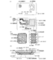
次に、突起部58を有するジグ52を、仮接着剤51を介して、薄膜集積回路装置50毎に取り付ける。ここで、ジグ(治具)とは、剥離層を除去した後に薄膜集積回路がバラバラに分離しないように、一時的に薄膜集積回路を固定する役割を有する。ジグの形状としては、図2(A)のように、後にハロゲン化フッ素を含む気体又は液体の導入を容易にするために、突起部を設けた櫛状の構造とするのが望ましいが、図4(C)のように平坦なジグ(55)を用いても構わない。突起部を有するジグ(治具、支持基板)を用いる場合には、基板をパターニングして用いればよい。また、ジグとしては、ハロゲン化フッ素によって冒されない酸化珪素を主成分とするガラス基板、石英基板、ステンレス(SUS)基板等を用いることができるが、ハロゲン化フッ素によって冒されない材料であれば、これらに限定されるものではない。また、ジグと薄膜集積回路との間には、仮接着するための接着剤が設けられている。 Next, the jig 52 having the protrusions 58 is attached to each thin film integrated circuit device 50 via the temporary adhesive 51. Here, the jig (jig) has a role of temporarily fixing the thin film integrated circuit so that the thin film integrated circuit is not separated after the peeling layer is removed. As shown in FIG. 2A, the shape of the jig is preferably a comb-like structure provided with protrusions in order to facilitate introduction of a gas or liquid containing halogenated fluorine later. You may use a flat jig (55) like 4 (C). When using a jig (a jig or a support substrate) having a protrusion, the substrate may be patterned. Moreover, as a jig, a glass substrate, a quartz substrate, a stainless steel (SUS) substrate, etc., mainly composed of silicon oxide that is not affected by halogenated fluorine can be used. It is not limited to. In addition, an adhesive for temporary bonding is provided between the jig and the thin film integrated circuit.
ここで、接着剤としては、UV光照射によって接着力(粘着力)が低下又は喪失する材料を用いることができる。ここでは、日東電工社製UV照射剥離テープを用いた。これ以外にも、前述した再剥離再接着可能な接着剤を用いても構わない。例えば、特開2001−30403、特許2992092、特開平6−299127に記載された、アクリル系粘着剤、合成ゴム系粘着剤、天然ゴム系粘着剤等を用いることができる。勿論、ジグを簡単に取り外すことができる材料であれば、これらに限定されるものではない。 Here, as the adhesive, a material whose adhesive strength (adhesive strength) is reduced or lost by UV light irradiation can be used. Here, a UV irradiation peeling tape manufactured by Nitto Denko Corporation was used. In addition to this, the above-described re-peelable and re-adhesive adhesive may be used. For example, an acrylic pressure-sensitive adhesive, a synthetic rubber pressure-sensitive adhesive, a natural rubber pressure-sensitive adhesive and the like described in JP-A-2001-30403, JP-A-2992092, and JP-A-6-299127 can be used. Of course, the material is not limited to these as long as the jig can be easily removed.
次に、溝93にハロゲン化フッ素ガスを導入することにより、剥離層であるa−Si膜をエッチング除去した(図2(A))。ここで用いた減圧CVD装置(図26)は、反応空間であるベルジャー89内に、ClF3ガス53等のハロゲン化フッ素ガスが導入され、ガスが基板90に行き渡る仕組みになっている。また、ベルジャーの外部にはヒーター91が設けられ、残余ガスは、排気管92から排出される。ここでは、図26に示すような減圧CVD装置を用い、ガス:ClF3、温度:350℃、流量:300sccm、気圧:6Torr、時間:3hの条件でa−Si膜のエッチング除去を行ったが、この条件に限定されるものではない。また、ClF3ガスに窒素を混ぜたガスを用いてもよい。両者の流量比は適宜設定することができる。
Next, a halogenated fluorine gas was introduced into the
ここで、ClF3等のハロゲン化フッ素は、珪素を選択的にエッチングするという特性がある反面、酸化珪素、窒化珪素、酸窒化珪素はほとんどエッチングされない。したがって、時間の経過ととも剥離層はエッチングされ、最終的に熱酸化シリコン基板41を剥離することができる(図2(B))。一方、酸化珪素、窒化珪素、酸窒化珪素等や、耐熱性樹脂からなる下地膜や、層間絶縁膜、保護膜はほとんどエッチングされないため、薄膜集積回路への損傷を防止することができる。なお、剥離した熱酸化シリコン基板41の表面は、酸化珪素等の絶縁膜で覆われているため、ClF3等のハロゲン化フッ素によって冒されることなく、再利用することができ、コスト削減に繋がる。
Here, fluorine halide such as ClF 3 has a characteristic of selectively etching silicon, but silicon oxide, silicon nitride, and silicon oxynitride are hardly etched. Therefore, the peeling layer is etched with time, and finally the thermally oxidized
次に、UV光照射を行うことにより、仮接着剤51の粘着力を低下又は喪失させ、ジグと、薄膜集積回路装置とを分離する(図2(C))。これにより、薄膜集積回路装置を大量に作製することができる。なお、ジグは、コスト削減のため、再利用するのが望ましい。 Next, the adhesive strength of the temporary adhesive 51 is reduced or lost by performing UV light irradiation, and the jig and the thin film integrated circuit device are separated (FIG. 2C). Thus, a large number of thin film integrated circuit devices can be manufactured. It is desirable to reuse the jig for cost reduction.
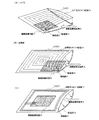
上記方法によって作製された薄膜集積回路装置50は、小型真空ピンセット13等により、搬送し、所望の製品に備え付けることができる。図3は、商品10に貼付されるIDラベル15の作製方法を示したものである。ラベル11に薄膜集積回路装置50を小型真空ピンセット13により貼り付け、接着剤14で封止し、IDラベル15が完成する。さらに、商品10にIDラベル15を付して、リーダ/ライタ等によって情報を認識、更新、管理しうる商品が完成する。 The thin film integrated circuit device 50 manufactured by the above method can be transported by a small vacuum tweezers 13 or the like and provided in a desired product. FIG. 3 shows a method for producing the ID label 15 attached to the product 10. The thin film integrated circuit device 50 is affixed to the label 11 with small vacuum tweezers 13 and sealed with an adhesive 14 to complete the ID label 15. Further, an ID label 15 is attached to the product 10, and a product that can be recognized, updated, and managed by a reader / writer or the like is completed.
あるいは、上記方法によって作製された薄膜集積回路装置50は、例えば、図10(A)に示すように、接着剤801を介してカバー800によって封止してもよい。なお、図10(B)は、封止状態の斜視図を示すものである。
Alternatively, the thin film integrated circuit device 50 manufactured by the above method may be sealed with a
(実施形態2)
本実施形態では、溝93を形成するにあたり、ドライエッチング法を用いる場合について、図4を用いて説明する。実施形態1の記載に基づいて、図1(A)に示す保護膜49の形成までを行う。その後、現像、露光工程を経て、基板上にレジスト54を形成し、レジスト54をマスクとして、ドライエッチングにより溝93を形成し、素子分離を行う(図4(A))。ここでは、プラズマエッチングを採用し、エッチング用ガスとしては、Cl2、BCl3、SiCl4もしくはCCl4などを代表とする塩素系ガス、CF4、SF6、NF3、CHF3などを代表とするフッ素系ガス、あるいはO2を用いたが、これらに限定されるものではない。なお、該エッチングは、大気圧プラズマを利用して行うこともできる。この際、エッチングガスとしては、CF4とO2の混合ガスを用いるのがよい。また、ガス種の異なるエッチングを複数回行うことによって溝93を形成しても良い。
(Embodiment 2)
In the present embodiment, a case where a dry etching method is used to form the
エッチングを行った後、レジスト54はそのまま残し、薄膜集積回路装置を保護するための保護膜として機能させた(図4(B))。なお、エッチングによって溝を形成する際のマスクとしては、レジストの他にも、ポリイミド、アクリル、ポリアミド、ベンゾシクロブテン、シリコンと酸素との結合で骨格構造が構成され、置換基に少なくとも水素を含む材料、若しくは置換基にフッ素、アルキル基、または芳香族炭化水素のうち少なくとも一種を有する材料等の絶縁膜を用いることができる。勿論、マスクとして用いられるこれらの絶縁膜は、上記エッチングの後、O2アッシング等によって除去しても構わない。 After the etching, the resist 54 is left as it is to function as a protective film for protecting the thin film integrated circuit device (FIG. 4B). As a mask for forming a groove by etching, in addition to a resist, a skeleton structure is composed of a bond of polyimide, acrylic, polyamide, benzocyclobutene, silicon and oxygen, and the substituent contains at least hydrogen. An insulating film such as a material or a material having at least one of fluorine, an alkyl group, and aromatic hydrocarbon as a substituent can be used. Of course, these insulating films used as a mask may be removed by O 2 ashing or the like after the etching.
次に、仮接着剤51を介して、ジグ55を薄膜集積回路装置50に取り付け、ClF3ガス53等のハロゲン化フッ素によって、剥離層を除去し、最終的に熱酸化シリコン基板41を剥離した(図4(B))。具体的な方法は、実施形態1と同様である。なお、ジグ55として、ここでは、突起部を特に設けていない基板を用いたが、勿論、突起部を有した基板を用いてもよい。なお、図4(B)のジグにおいて、ClF3ガス53等のハロゲン化フッ素が、剥離層に供給されやすいように、孔700を設けた。孔700は、ジグが薄膜集積回路装置の保持に支障がない程度に設けておくのが望ましい。
Next, the jig 55 is attached to the thin film integrated circuit device 50 via the temporary adhesive 51, and the release layer is removed by halogenated fluorine such as ClF 3 gas 53. Finally, the thermally oxidized
次に、UV光照射を行うことにより、仮接着剤51の粘着力を低下又は喪失させ、ジグ55と、薄膜集積回路装置50とを分離することにより、薄膜集積回路装置を大量に作製することができる。上記方法によって作製された薄膜集積回路装置50は、小型真空ピンセット等により、搬送し、所望の製品に備え付けることができる。 Next, the adhesive strength of the temporary adhesive 51 is reduced or lost by performing UV light irradiation, and the jig 55 and the thin film integrated circuit device 50 are separated to manufacture a large number of thin film integrated circuit devices. Can do. The thin film integrated circuit device 50 manufactured by the above method can be transported by a small vacuum tweezers or the like and provided in a desired product.
(実施形態3)
本実施形態では、ダイシング等によって溝93を形成する際に、熱酸化シリコン基板41やSIMOX基板等のSOI基板に傷が付いた場合、それらの基板を再利用する場合について説明する。まず、図5(A)に示すように、使用済み基板56上に平坦化膜57を形成する。平坦化膜としては、ポリイミド、アクリル、ポリアミドや、シロキサン等の耐熱性樹脂を、スピンコート法、ディップ法、スプレー法、液滴吐出法(インクジェット法等)等によって形成することができる。後工程の熱処理を考慮すれば、シロキサン等の耐熱性樹脂を用いることが望ましい。また、無機材料を用いてもよく、その際には、PSG、BPSG、アルミナ膜等を用いることができる。その後、実施形態1又は2に基づいて薄膜集積回路を作製、分離して所望の製品に備え付けることができる。
(Embodiment 3)
In the present embodiment, when the
他の方法として、図6(A)に示すように、CMP(機械的化学的研磨)法、プレス法、エッチバック法等により、基板表面を平坦化する方法がある。使用済み基板56の傷が微細である場合に特に有効である。CMP法は、研磨用パッド308内にスラリー(307)と呼ばれる研磨溶剤を供給し、ウエハキャリア306の回転とプラテンと呼ばれる回転台の回転による加圧と、研磨用パッドの研磨によって平坦化を行うものである。基板は、ガラス基板のように絶縁体であるので、スラリー307としては、アルカリ性のコロイド状シリカを混ぜたものが主に用いられる。また、プレス法(図6(B))の場合には、ヒーター301等の加熱機構を備えた装置300によってプレスを行うのがよい。また、エッチバック法(図6(C))では、絶縁膜309を平坦に形成した後に、エッチングを行って、平坦化するものである。その後、実施形態1又は2に基づいて薄膜集積回路を作製、分離して所望の製品に備え付けることができる。
As another method, as shown in FIG. 6A, there is a method of planarizing the substrate surface by a CMP (mechanical chemical polishing) method, a press method, an etch back method, or the like. This is particularly effective when the scratches on the used substrate 56 are fine. In the CMP method, a polishing solvent called slurry (307) is supplied into the polishing pad 308, and planarization is performed by the rotation of the wafer carrier 306 and the rotation of a turntable called a platen, and polishing of the polishing pad. Is. Since the substrate is an insulator like a glass substrate, as the slurry 307, a mixture of alkaline colloidal silica is mainly used. In the case of the pressing method (FIG. 6B), the pressing is preferably performed by the
(実施形態4)
上記実施形態では、薄膜集積回路の作製工程において、アンテナを形成したが、本実施形態では、基板上に作製されたアンテナと、複数の薄膜集積回路を別々に作製し、その後両者を接続する方法について、図7〜図12を参照して説明する。
(Embodiment 4)
In the above embodiment, the antenna is formed in the manufacturing process of the thin film integrated circuit. However, in this embodiment, the antenna manufactured on the substrate and a plurality of thin film integrated circuits are separately manufactured, and then both are connected. Will be described with reference to FIGS.
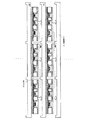
第1の方法は、図7(A)に示すように、折り曲げ可能なフレキシブル基板69上に、アンテナ68を形成し、別途形成した薄膜集積回路25を図7(B)に示すアンテナの接続部99と接続した後に、フレキシブル基板69を図7(C)に示すように矢印の方向に半分に折りたたみ、封止して薄膜集積回路装置を作製するというものである。ここで、アンテナ68は、スパッタ法等によって形成した後にパターニング形成しても良いし、液滴吐出法を用い、導電材料を含む組成物を選択的に吐出した後に、該組成物を乾燥、焼成することにより形成しても良い。
In the first method, as shown in FIG. 7A, an antenna 68 is formed on a foldable
なお、アンテナを形成した後に、図6(A)〜図6(C)に示す、CMP法、プレス法、エッチバック法等により、平坦性を向上させても良い。CMP法の場合には、アンテナは導電性材料からなるので、スラリーとしては、酸性溶液にアルミナの微粉末を混ぜたものを用いるのがよい。また、プレス法の場合には、ヒーター301等の加熱機構を備えた装置によってプレスを行うのがよい。また、エッチバック法では、絶縁膜309を平坦に形成した後に、エッチングを行って、平坦化するものである。なお、これらの平坦化処理工程は、薄膜集積回路の作製工程において用いることもできる。
Note that after the antenna is formed, planarity may be improved by a CMP method, a press method, an etch back method, or the like shown in FIGS. In the case of the CMP method, since the antenna is made of a conductive material, it is preferable to use a slurry obtained by mixing a fine powder of alumina in an acidic solution. In the case of the pressing method, the pressing is preferably performed by an apparatus having a heating mechanism such as a heater 301. In the etch back method, after the insulating
アンテナには、アンテナ同士を接続する接続部98や、アンテナと集積回路を接続する接続部99を、アンテナ形成時に形成しておいても良い。また、集積回路との接続部99は、アンテナを形成した後に、アンテナの一部を切断することによって形成しても良い。なお、薄膜集積回路とアンテナとの接続は、異方性導電膜や、公知のボンディング法等を用いて行うことができる。また、アンテナの形状は、折り畳んだときに対称でコイル状であれば、図7に示す形状に限定されない。 The antenna may be formed with a connection part 98 for connecting the antennas and a connection part 99 for connecting the antenna and the integrated circuit when the antenna is formed. Further, the connection portion 99 with the integrated circuit may be formed by cutting a part of the antenna after forming the antenna. Note that the thin film integrated circuit and the antenna can be connected using an anisotropic conductive film, a known bonding method, or the like. Further, the shape of the antenna is not limited to the shape shown in FIG. 7 as long as it is symmetrical and coiled when folded.
アンテナ基板に挟まれる薄膜集積回路25は、図18に示すように、電源回路26、入出力回路27、論理回路28、メモリ29、CPU30等に、リーダ/ライタ136との電波のやりとりを行うアンテナ回路が接続された構成を有している。
As shown in FIG. 18, the thin film integrated circuit 25 sandwiched between the antenna substrates is an antenna for exchanging radio waves with the reader / writer 136 to the power circuit 26, the input / output circuit 27, the logic circuit 28, the memory 29, the
なお、図8(A)〜図8(E)は、図7(C)のX−Y断面から見たアンテナ基板折り畳みの状態を示した図である。ここでは、アンテナ20をパターニング形成する際に用いたレジスト23をアッシング等によって除去してしまわずに、残存させた(図8(A))。さらに、平坦化膜60をスピンコート法、ディップ法、スプレー法、液滴吐出法等によって形成し、平坦化を行った(図8(B))。さらに、薄膜集積回路25との接続部を確保するために、レジスト61をマスクとして、エッチング又はアッシングを行い、コンタクト部62を形成した(図8(C))。さらに、異方性導電膜63を介して薄膜集積回路25を形成し、シール剤64を介して、アンテナが形成されたフレキシブル基板19を折り畳(図8(D))み、薄膜集積回路装置(IDチップ)66を完成させた(図8(E))。この際、対向するアンテナ同士の間に配線等を設けてアンテナ同士を接続しても良い。ここで、レジスト23や平坦化膜60は、基板を折り畳んだ際に、アンテナや薄膜集積回路を保護するクッションの役割を果たす。なお、レジスト23や平坦化膜60は、一方又は両方を省略することもできる。 FIGS. 8A to 8E are views showing the folded state of the antenna substrate viewed from the XY cross section of FIG. 7C. Here, the resist 23 used for patterning the antenna 20 is left without being removed by ashing or the like (FIG. 8A). Further, the planarization film 60 was formed by a spin coating method, a dip method, a spray method, a droplet discharge method, or the like, and planarization was performed (FIG. 8B). Further, in order to secure a connection portion with the thin film integrated circuit 25, etching or ashing was performed using the resist 61 as a mask to form a contact portion 62 (FIG. 8C). Further, the thin film integrated circuit 25 is formed through the anisotropic conductive film 63, and the flexible substrate 19 on which the antenna is formed is folded through the sealant 64 (FIG. 8D), so that the thin film integrated circuit device is obtained. (ID chip) 66 was completed (FIG. 8E). At this time, the antennas may be connected by providing wiring or the like between the opposing antennas. Here, the resist 23 and the planarizing film 60 serve as a cushion for protecting the antenna and the thin film integrated circuit when the substrate is folded. One or both of the resist 23 and the planarizing film 60 can be omitted.
第2の方法は、図9(A)、図9(B)に示すように、基板67上にアンテナ68を複数形成しておき、基板67をダイシング等によって切り出し、アンテナ基板の間に薄膜集積回路25を挟む方法である。ここで、接続部21は、アンテナ同士を接続するために用いてもよいし、薄膜集積回路とアンテナとを接続するのに用いてもよい。また、接続部21は、アンテナの他の箇所に形成しても良い。なお、基板同士を貼り合わせる際に、アライメントマーカーを設ける必要があるが、該接続部21をマーカーとしても良い。 In the second method, as shown in FIGS. 9A and 9B, a plurality of antennas 68 are formed on a substrate 67, the substrate 67 is cut out by dicing or the like, and a thin film is integrated between the antenna substrates. In this method, the circuit 25 is sandwiched. Here, the connecting portion 21 may be used for connecting the antennas, or may be used for connecting the thin film integrated circuit and the antenna. Moreover, you may form the connection part 21 in the other location of an antenna. In addition, although it is necessary to provide an alignment marker when bonding substrates together, this connection part 21 is good also as a marker.
第3の方法は、図11に示すように、二方が閉じられた食品を包装するラップ状のフレキシブル基板70や、三方が閉じられた封筒状のフレキシブル基板74に、アンテナ71を両面に形成しておき、その間に薄膜集積回路25を挿入し、接着剤73で封止するという方法である。接続部21は開孔されており、アンテナ同士、又はアンテナと薄膜集積回路が接続することができる。ICチップは小型真空ピンセット等で設置すればよい。なお、アンテナは、これらの基板の内側に形成しておいても良い。
In the third method, as shown in FIG. 11,
なお、これらの封止状態の断面図を図12に示す。薄膜集積回路25とアンテナ71を接続するための接続端子803は、図12(A)(B)に例示するように、所望の箇所に設けることができる。接続方法としては、図示する異方性導電膜802による方法の他、COG方法やワイヤボンディング方法、或いはTAB方法など、公知の方法を用いることができる。
A sectional view of these sealed states is shown in FIG. The connection terminal 803 for connecting the thin film integrated circuit 25 and the
以上、本実施形態で述べた薄膜集積回路装置の作製方法は、特に、アンテナ基板と、薄膜集積回路とを別々の製造者が作製し、中間生成品(部品)として流通させる場合に適した方法である。 As described above, the method for manufacturing the thin film integrated circuit device described in the present embodiment is particularly suitable for a case where the antenna substrate and the thin film integrated circuit are manufactured by different manufacturers and distributed as intermediate products (components). It is.
(実施形態5)
本実施形態では、図24を参照して、素子基板75に仮接着したジグ76を取り外さずに、直接、商品84等に接着する方法について説明する。まず、実施形態1〜3に基づいて、素子基板75を形成し、仮接着剤81を介してジグ76を取り付ける。ジグ76としては、図24(A)、図24(B)に示すように、突起部77を有するものを用いた。仮接着剤81としては、ここでは、UV光照射によって粘着力が低下又は喪失する材料を用いる。また、素子への損傷を防ぐために、有機材料又は無機材料からなる層間膜79を設けている。そして、ClF3等のハロゲン化フッ素によるエッチングにより、素子分離を行う。
(Embodiment 5)
In the present embodiment, a method of directly bonding to the product 84 or the like without removing the jig 76 temporarily bonded to the element substrate 75 will be described with reference to FIG. First, the element substrate 75 is formed based on the first to third embodiments, and the jig 76 is attached via the temporary adhesive 81. As the jig 76, as shown in FIG. 24A and FIG. Here, as the temporary adhesive 81, a material whose adhesive strength is reduced or lost by UV light irradiation is used. In order to prevent damage to the element, an interlayer film 79 made of an organic material or an inorganic material is provided. Then, element isolation is performed by etching with a halogenated fluorine such as ClF 3 .
次に、ジグ76に素子が仮接着された状態で搬送し、IDカード等の商品84が設置されたステージとのアライメントを行う。この際、図24(A)に示すように、ジグや、ステージに設けられたアライメントマーカー78、82を利用することもできるし、図示しないが、商品84に形成されたマーカーを利用することもできる。商品84内の薄膜集積回路装置が形成される部分には、予め接着剤85が形成されており、ジグを制御することにより、所望の素子を商品の所望の箇所に貼り付ける(図24(A))。
Next, the device is transported in a state where the elements are temporarily bonded to the jig 76, and aligned with a stage on which a product 84 such as an ID card is installed. At this time, as shown in FIG. 24A, jigs and
次に、商品84に貼り付けたい素子に、マスクを介してUV光86を選択的に照射し、仮接着剤81の粘着力を低下又は喪失させることにより、ジグを素子とを分離する(図24(B))。これにより、所望の素子(集積回路87)を商品の所望の箇所に形成することができる。素子形成後、カバー88等により、素子部をカバーする(図24(C))。なお、ここでは、商品84の内部にアンテナ83が形成された場合を示したが、素子部にアンテナを形成しておいても良い。
Next, the element to be attached to the product 84 is selectively irradiated with UV light 86 through a mask, and the adhesive strength of the temporary adhesive 81 is reduced or lost, thereby separating the jig from the element (see FIG. 24 (B)). Thereby, a desired element (integrated circuit 87) can be formed in a desired location of the product. After element formation, the element portion is covered with a
本実施形態に示した本発明を用いることにより、ClF3等のハロゲン化フッ素によるエッチングにより素子分離を行った際、素子がバラバラに分離することなく、所望の素子を所望の箇所に形成することができる。 By using the present invention shown in this embodiment, when elements are separated by etching with a halogenated fluorine such as ClF 3 , a desired element is formed at a desired position without being separated. Can do.
本実施例では、図13、14を参照して、薄膜集積回路装置の集積回路部の具体的な作製方法について説明する。ここでは、簡単のため、nチャネル型TFTとpチャネル型TFTを用いたCPUとメモリの作製方法について説明する。 In this embodiment, a specific method for manufacturing an integrated circuit portion of a thin film integrated circuit device will be described with reference to FIGS. Here, for simplicity, a method for manufacturing a CPU and a memory using an n-channel TFT and a p-channel TFT will be described.
まず、熱酸化シリコン基板41上に、剥離層43と、下地膜44を形成する(図13(A))。これらの材料や作製方法は、実施形態1〜実施形態5に述べたものを採用することができる。 First, a peeling layer 43 and a base film 44 are formed over a thermally oxidized silicon substrate 41 (FIG. 13A). As these materials and manufacturing methods, those described in Embodiments 1 to 5 can be adopted.
次に、下地膜44上に、島状半導体膜100を形成する(図13(B))。島状半導体膜100は、アモルファス半導体、結晶性半導体、又はセミアモルファス半導体で形成する。いずれも、シリコン、シリコン・ゲルマニウム(SiGe)等を主成分とする半導体膜を用いることができる。 Next, the island-shaped semiconductor film 100 is formed over the base film 44 (FIG. 13B). The island-shaped semiconductor film 100 is formed using an amorphous semiconductor, a crystalline semiconductor, or a semi-amorphous semiconductor. In any case, a semiconductor film containing silicon, silicon germanium (SiGe), or the like as a main component can be used.
本実施例では、70nmの膜厚のアモルファスシリコンを形成し、さらにその表面を、シリコンの結晶化を促進する触媒元素、例えばニッケルを含む溶液で処理した後、500〜750℃の熱結晶化工程によって結晶性シリコン膜を得、さらにレーザー結晶化を行って結晶性の改善を施した。また、成膜方法としては、プラズマCVD法、スパッタ法、LPCVD法などを用いても良いし、結晶化方法としては、レーザー結晶化法、熱結晶化法、他の触媒元素(Fe,Ru,Rh,Pd,Os,Ir,Pt,Cu,Au等)を用いた熱結晶化、あるいはそれらを交互に複数回行っても良い。 In this example, amorphous silicon having a film thickness of 70 nm is formed, and the surface thereof is further treated with a solution containing a catalytic element that promotes crystallization of silicon, such as nickel, and then a thermal crystallization process at 500 to 750 ° C. Thus, a crystalline silicon film was obtained, and further crystallized by laser crystallization. Further, as a film formation method, a plasma CVD method, a sputtering method, an LPCVD method, or the like may be used. As a crystallization method, a laser crystallization method, a thermal crystallization method, or other catalytic elements (Fe, Ru, Rh, Pd, Os, Ir, Pt, Cu, Au, etc.) or they may be alternately performed a plurality of times.
また、非晶質構造を有する半導体膜の結晶化処理としては、連続発振のレーザーを用いても良く、結晶化に際し大粒径の結晶を得るためには、連続発振が可能な固体レーザーを用い、基本波の第2高調波〜第4高調波を適用するのが好ましい。代表的には、Nd:YVO4レーザー(基本波1064nm)の第2高調波(532nm)や第3高調波(355nm)を適用すればよい。連続発振のレーザーを用いる場合には、出力10Wの連続発振のYVO4レーザーから射出されたレーザー光を非線形光学素子により高調波に変換する。また、共振器の中にYVO4結晶と非線形光学素子を入れて、高調波を射出する方法もある。そして、好ましくは光学系により照射面にて矩形状または楕円形状のレーザー光に成形して、被処理体に照射する。このときのエネルギー密度は0.01〜100MW/cm2程度、好ましくは0.1〜10MW/cm2が必要である。そして、10〜2000cm/s程度の速度でレーザー光に対して相対的に半導体膜を移動させて照射すればよい。 In addition, a continuous wave laser may be used for the crystallization treatment of the semiconductor film having an amorphous structure, and a solid laser capable of continuous oscillation is used in order to obtain a crystal having a large particle size upon crystallization. It is preferable to apply the second to fourth harmonics of the fundamental wave. Typically, a second harmonic (532 nm) or a third harmonic (355 nm) of an Nd: YVO 4 laser (fundamental wave 1064 nm) may be applied. In the case of using a continuous wave laser, laser light emitted from a continuous wave YVO 4 laser having an output of 10 W is converted into a harmonic by a non-linear optical element. There is also a method of emitting harmonics by putting a YVO 4 crystal and a nonlinear optical element in a resonator. Preferably, the laser beam is shaped into a rectangular or elliptical shape on the irradiation surface by an optical system, and the object to be processed is irradiated. At this time, the energy density of 0.01 to 100 MW / cm 2 or so, preferably requires 0.1 to 10 MW / cm 2. Then, irradiation may be performed by moving the semiconductor film relative to the laser light at a speed of about 10 to 2000 cm / s.
上記の方法によって結晶性シリコン膜を得た後、半導体膜上に酸化シリコン膜を介して、触媒元素をゲッタリングするためのアモルファスシリコン膜を成膜し、500〜750℃の熱処理によってゲッタリング処理を行った。さらに、TFT素子としての閾値を制御するために、結晶性シリコン膜に対し、1013/cm2オーダーのドーズ量のホウ素イオンを注入した。その後、レジストをマスクとしてエッチングを行うことにより、島状半導体膜100を形成した。 After obtaining the crystalline silicon film by the above method, an amorphous silicon film for gettering the catalytic element is formed on the semiconductor film via the silicon oxide film, and gettering treatment is performed by heat treatment at 500 to 750 ° C. Went. Furthermore, in order to control the threshold value as the TFT element, boron ions having a dose of the order of 10 13 / cm 2 were implanted into the crystalline silicon film. Then, the island-shaped semiconductor film 100 was formed by performing etching using the resist as a mask.
なお、結晶性半導体膜を形成するにあたっては、ジシラン(Si2H6)とフッ化ゲルマニウム(GeF4)を原料ガスとして、LPCVD(減圧CVD)法によって、多結晶半導体膜を直接形成することによっても、結晶性半導体膜を得ることができる。ガス流量比は、Si2H6/GeF4=20/0.9、成膜温度は400〜500℃、キャリアガスとしてHe又はArを用いたが、これに限定されるものではない。 In forming a crystalline semiconductor film, a polycrystalline semiconductor film is directly formed by LPCVD (low pressure CVD) using disilane (Si 2 H 6 ) and germanium fluoride (GeF 4 ) as source gases. Also, a crystalline semiconductor film can be obtained. The gas flow ratio is Si 2 H 6 / GeF 4 = 20 / 0.9, the film forming temperature is 400 to 500 ° C., and He or Ar is used as the carrier gas, but the present invention is not limited to this.
次に、島状半導体膜100上にゲート絶縁膜102を形成する(図13(B))。ゲート絶縁膜102はプラズマCVD法又はスパッタリング法などの薄膜形成法を用い、窒化珪素、酸化珪素、窒化酸化珪素又は酸化窒化珪素を含む膜を、単層で、又は積層させて形成することが好ましい。積層する場合には、例えば、基板側から酸化珪素膜、窒化珪素膜、酸化珪素膜の3層構造とするのがよい。 Next, the gate insulating film 102 is formed over the island-shaped semiconductor film 100 (FIG. 13B). The gate insulating film 102 is preferably formed using a thin film formation method such as a plasma CVD method or a sputtering method, and a film containing silicon nitride, silicon oxide, silicon nitride oxide, or silicon oxynitride is formed as a single layer or stacked layers. . In the case of stacking, for example, a three-layer structure of a silicon oxide film, a silicon nitride film, and a silicon oxide film is preferable from the substrate side.
次に、ゲート電極103を形成する(図13(C))。本実施例では、30nmの膜厚のTaN(窒化タンタル)と、370nmの膜厚のW(タングステン)をスパッタ法により積層形成した後に、レジスト104をマスクとしてエッチングを行うことにより、ゲート電極103を形成した。ここで、レジストマスクの代わりに、SiOx(酸化珪素)等のマスクを用いてもよい。この場合、SiOx、SiON等のマスク(ハードマスクと呼ばれる。)をパターニング形成工程が加わるが、エッチング時におけるマスクの膜減りがレジストよりも少ないため、所望の幅のゲート電極103を形成することができる。勿論、ゲート電極103の材料、構造、作製方法は、これに限定されるものではなく、適宜選択することができる。例えば、レジスト104を用いずに、液滴吐出法を用いて選択的にゲート電極103を形成しても良い。 Next, the gate electrode 103 is formed (FIG. 13C). In this embodiment, TaN (tantalum nitride) with a thickness of 30 nm and W (tungsten) with a thickness of 370 nm are stacked by sputtering, and then etched using the resist 104 as a mask, whereby the gate electrode 103 is formed. Formed. Here, a mask made of SiOx (silicon oxide) or the like may be used instead of the resist mask. In this case, a patterning process is added to a mask (referred to as a hard mask) of SiOx, SiON, or the like. However, since the film thickness of the mask during etching is less than that of the resist, the gate electrode 103 having a desired width may be formed. it can. Needless to say, the material, structure, and manufacturing method of the gate electrode 103 are not limited to these, and can be selected as appropriate. For example, the gate electrode 103 may be selectively formed using a droplet discharge method without using the resist 104.
なお、ゲート電極103を形成するための導電材料としては、導電膜の機能に応じて種々の材料を選択することができるが、代表的なものとして、銀(Ag)、銅(Cu)、金(Au)、ニッケル(Ni)、白金(Pt)、クロム(Cr)、スズ(Sn)、パラジウム(Pd)、イリジウム(Ir)、ロジウム(Rh)、ルテニウム(Ru)、レニウム(Re)、タングステン(W)、アルミニウム(Al)、タンタル(Ta)、インジウム(In)、テルル(Te)、モリブデン(Mo)、カドミウム(Cd、亜鉛(Zn)、鉄(Fe)、チタン(Ti)、シリコン(Si)、ゲルマニウム(Ge)、ジルコニウム(Zr)、バリウム(Ba)、アンチモン鉛、酸化スズ・アンチモン、フッ素ドープ酸化亜鉛、炭素、グラファイト、グラッシーカーボン、リチウム、ベリリウム、マグネシウム、カリウム、カルシウム、スカンジウム、マンガン、ガリウム、ニオブ、ナトリウム、ナトリウム−カリウム合金、マグネシウム/銅混合物、マグネシウム/銀混合物、マグネシウム/アルミニウム混合物、マグネシウム/インジウム混合物、アルミニウム/酸化アルミニウム混合物、リチウム/アルミニウム混合物等、ハロゲン化銀の微粒子等、又は分散性ナノ粒子、あるいは、透明導電膜として用いられる酸化インジウムスズ(ITO:Indium Tin Oxide)、ITSO(ITOに珪素又は酸化珪素を含有させたもの)、酸化亜鉛(ZnO:Zinc Oxide)、ガリウムを添加した酸化亜鉛(GZO)、酸化インジウムに2〜20%の酸化亜鉛を混合した酸化インジウム亜鉛(IZO:Indium Zinc Oxide)、有機インジウム、有機スズ、窒化チタン等を適宜採用することができる。 Note that a variety of materials can be selected as a conductive material for forming the gate electrode 103 depending on the function of the conductive film. Typical examples include silver (Ag), copper (Cu), and gold. (Au), nickel (Ni), platinum (Pt), chromium (Cr), tin (Sn), palladium (Pd), iridium (Ir), rhodium (Rh), ruthenium (Ru), rhenium (Re), tungsten (W), aluminum (Al), tantalum (Ta), indium (In), tellurium (Te), molybdenum (Mo), cadmium (Cd, zinc (Zn), iron (Fe), titanium (Ti), silicon ( Si), germanium (Ge), zirconium (Zr), barium (Ba), antimony lead, tin oxide / antimony, fluorine-doped zinc oxide, carbon, graphite, graphite Carbon, lithium, beryllium, magnesium, potassium, calcium, scandium, manganese, gallium, niobium, sodium, sodium-potassium alloy, magnesium / copper mixture, magnesium / silver mixture, magnesium / aluminum mixture, magnesium / indium mixture, aluminum / oxidation Aluminum mixtures, lithium / aluminum mixtures, etc., silver halide fine particles, etc., or dispersible nanoparticles, or indium tin oxide (ITO) used as a transparent conductive film, ITSO (ITO (silicon or silicon oxide is added to ITO) Zinc oxide (ZnO: Zinc Oxide), zinc oxide added with gallium (GZO), indium zinc oxide mixed with 2-20% zinc oxide in indium oxide (IZO: Indium Zinc Oxide) Organic indium, organotin, can be appropriately employed titanium nitride.
なお、ゲート電極103をエッチング形成する際のエッチングガスとしては、CF4、Cl2、及びO2の混合ガスやCl2ガスを用いたが、これに限定されるものではない。 Note that as the etching gas for forming the gate electrode 103 by etching, a mixed gas of CF 4 , Cl 2 , and O 2 or Cl 2 gas is used, but the present invention is not limited to this.
次に、pチャネル型TFT109,111となる部分をレジスト118で覆い、ゲート電極103をマスクとして、nチャネル型TFT108、110の島状半導体膜に、第1の不純物導入工程としてn型を付与する不純物元素119(代表的にはP(リン)又はAs(砒素))を低濃度に導入する(図13(D))。第1の不純物導入の条件は、ドーズ量:1×10¹³〜6×10¹³/cm2、加速電圧:50〜70keVとしたが、これに限定されるものではない。この第1の不純物導入によって、ゲート絶縁膜102を介してスルードープがなされ、一対の低濃度不純物領域120が形成される。なお、第1の不純物導入は、pチャネル型TFT領域をレジストで覆わずに、全面に行っても良い。
Next, the portions to be the p-channel TFTs 109 and 111 are covered with a resist 118, and the gate electrode 103 is used as a mask to give the n-type to the island-like semiconductor films of the n-channel TFTs 108 and 110 as a first impurity introduction step. An impurity element 119 (typically P (phosphorus) or As (arsenic)) is introduced at a low concentration (FIG. 13D). The first impurity introduction condition is a dose amount of 1 × 10 13 to 6 × 10 13 / cm 2 and an acceleration voltage of 50 to 70 keV, but is not limited thereto. By this first impurity introduction, through doping is performed through the gate insulating film 102, and a pair of low-
次に、レジスト118をアッシング等により除去した後、nチャネル型TFT領域を覆うレジスト121を新たに形成し、ゲート電極をマスクとして、pチャネル型TFT109、111の島状半導体膜に、第2の不純物導入工程としてpチャネル型を付与する不純物元素122(代表的にはB(ホウ素))を高濃度に導入する(図13(E))。第2の不純物導入の条件は、ドーズ量:1×10¹⁶〜3×10¹⁶/cm2、加速電圧:20〜40keVとして行う。この第2の不純物導入によって、ゲート絶縁膜102を介してスルードープがなされ、一対のp型の高濃度不純物領域123が形成される。
Next, after removing the resist 118 by ashing or the like, a resist 121 that covers the n-channel TFT region is newly formed, and the second semiconductor film is formed on the island-shaped semiconductor films of the p-channel TFTs 109 and 111 using the gate electrode as a mask. As an impurity introduction step, an impurity element 122 imparting a p-channel type (typically B (boron)) is introduced at a high concentration (FIG. 13E). The second impurity introduction condition is a dose amount of 1 × 10 16 to 3 × 10 16 / cm 2 and an acceleration voltage of 20 to 40 keV. By this second impurity introduction, through doping is performed through the gate insulating film 102, and a pair of p-type high-
次に、レジスト121をアッシング等により除去した後、基板表面に、絶縁膜105を形成した(図14(A))。ここでは、膜厚100nmのSiON(酸窒化珪素)膜と、膜厚200nmのLTO膜(Low Temperature Oxide、低温酸化膜)の2層構造とした。ここでは、SiON膜は、プラズマCVD法で形成し、低温酸化膜として、SiO2膜を減圧CVD法で形成した。その後、図示しないが、基板のTFTが形成された側をレジストで覆い、基板の裏面に形成された絶縁膜をエッチング除去した(裏面処理)。 Next, after removing the resist 121 by ashing or the like, an insulating film 105 was formed over the substrate surface (FIG. 14A). Here, a two-layer structure of a SiON (silicon oxynitride) film having a thickness of 100 nm and an LTO film (Low Temperature Oxide) having a thickness of 200 nm is used. Here, the SiON film was formed by the plasma CVD method, and the SiO 2 film was formed by the low pressure CVD method as the low temperature oxide film. Thereafter, although not shown, the side of the substrate on which the TFT was formed was covered with a resist, and the insulating film formed on the back surface of the substrate was removed by etching (back surface treatment).
次に、レジストを残したまま、エッチバック法により、レジスト及び絶縁膜105をエッチング除去し、サイドウォール(側壁)106を自己整合的(セルフアライン)に形成した(図14(B))。エッチングガスとしては、CHF3とHeの混合ガスを用いた。なお、サイドウォールを形成する工程は、これらに限定されるものではない。 Next, with the resist remaining, the resist and the insulating film 105 were removed by etching using an etch-back method, and sidewalls (sidewalls) 106 were formed in a self-aligned manner (FIG. 14B). As the etching gas, a mixed gas of CHF 3 and He was used. Note that the step of forming the sidewall is not limited to these.
次に、pチャネル型TFT領域を覆うレジスト124を新たに形成し、ゲート電極層103及びサイドウォール106をマスクとして、第3の不純物導入工程として、n型を付与する不純物元素125を高濃度に導入する(図14(C))。第3の不純物導入の条件は、ドーズ量:1×10¹³〜5×10¹⁵/cm2、加速電圧:60〜100keVとして行う。この第3の不純物導入によって、ゲート絶縁膜102を介してスルードープがなされ、一対のn型の高濃度不純物領域126が形成される。
Next, a resist 124 is newly formed to cover the p-channel TFT region, and the n-
なお、図示しないが、レジスト124をアッシング等により除去した後、不純物領域の熱活性化を行っても良い。例えば、50nmのSiON膜(酸窒化珪素膜)を成膜した後、550℃、4時間、窒素雰囲気下において、加熱処理を行えばよい。また、水素を含むSiNx膜を、100nmの膜厚に形成した後、410℃、1時間、窒素雰囲気下において、加熱処理を行うことにより、結晶性半導体膜の欠陥を改善することができる。これは、例えば、結晶性シリコン中に存在するダングリングボンドを終端させるものであり、水素化処理工程などと呼ばれる。さらに、この後、TFTを保護するキャップ絶縁膜として、膜厚600nmのSiON膜を形成する。なお、水素化処理工程は、該SiON膜形成後に行っても良い。この場合、SiNxの上にSiON膜を順次成膜した絶縁膜は連続成膜することができる。このように、TFT上には、基板側から、SiON、SiNx、SiONを順次積層した3層の絶縁膜が形成されることになるが、その構造や材料はこれらに限定されるものではない。また、これらの絶縁膜は、TFTを保護する機能をも有しているため、できるだけ形成しておくのが望ましい。 Although not shown, the impurity region may be thermally activated after the resist 124 is removed by ashing or the like. For example, after a 50 nm SiON film (silicon oxynitride film) is formed, heat treatment may be performed at 550 ° C. for 4 hours in a nitrogen atmosphere. In addition, after the SiNx film containing hydrogen is formed to a thickness of 100 nm, defects in the crystalline semiconductor film can be improved by performing heat treatment at 410 ° C. for 1 hour in a nitrogen atmosphere. This terminates dangling bonds existing in, for example, crystalline silicon, and is called a hydrogenation process. Thereafter, a SiON film having a film thickness of 600 nm is formed as a cap insulating film for protecting the TFT. Note that the hydrogenation process may be performed after the formation of the SiON film. In this case, the insulating film in which the SiON film is sequentially formed on SiNx can be continuously formed. As described above, a three-layer insulating film in which SiON, SiNx, and SiON are sequentially stacked is formed on the TFT from the substrate side, but the structure and material are not limited to these. In addition, these insulating films have a function of protecting the TFT, so that it is desirable to form them as much as possible.
次に、TFT上に、層間絶縁膜107を形成する。層間絶縁膜107として、ポリイミド、アクリル、ポリアミドや、シロキサン等の耐熱性有機樹脂を用いることができる。形成方法としては、その材料に応じて、スピンコート、ディップ、スプレー塗布、液滴吐出法、ドクターナイフ、ロールコーター、カーテンコーター、ナイフコーター等を採用することができる。また、無機材料を用いてもよく、その際には、PSG、BPSG、アルミナ膜等を用いることができる。なお、これらの絶縁膜を積層させて、層間絶縁膜107を形成しても良い。 Next, an interlayer insulating film 107 is formed over the TFT. As the interlayer insulating film 107, a heat-resistant organic resin such as polyimide, acrylic, polyamide, or siloxane can be used. As a forming method, a spin coat, dip, spray coating, droplet discharge method, doctor knife, roll coater, curtain coater, knife coater, or the like can be employed depending on the material. In addition, an inorganic material may be used, and in that case, PSG, BPSG, an alumina film, or the like can be used. Note that the insulating interlayer 107 may be formed by stacking these insulating films.
次に、レジストを形成した後、エッチングによりコンタクトホールを開孔し、配線128及びアンテナ48を形成する(図14(D))。コンタクトホール開孔時のエッチングに用いられるガスは、CHF3とHeの混合ガスを用いたが、これに限定されるものではない。
Next, after forming a resist, a contact hole is formed by etching, so that a
また、配線128とアンテナ48は同一材料を用いて同時に形成しても良いし、別々に形成しても良い。ここでは、TFTと接続される配線128は、基板側から、Ti、TiN、Al−Si、Ti、TiNを順次積層した5層構造とし、スパッタ法によって形成した後、パターニング形成した。
Further, the
なお、Al層において、Siを混入させることにより、配線パターニング時のレジストベークにおけるヒロックの発生を防止することができる。また、Siの代わりに、0.5%程度のCuを混入させても良い。また、TiやTiNでAl−Si層をサンドイッチすることにより、耐ヒロック性がさらに向上する。なお、パターニング時には、窒素を含む酸化珪素(SiON)等からなる上記ハードマスクを用いるのが望ましい。なお、配線の材料や、形成方法はこれらに限定されるものではなく、前述したゲート電極に用いられる材料を採用しても良い。また、アンテナ48を形成する際には、上記実施の形態に示した、種々の材料、方法を用いることができる。配線とアンテナは、同時に形成しても良いし、一方を先に形成した後に、他方が乗り上げるように形成しても良い。 In addition, by mixing Si in the Al layer, generation of hillocks in resist baking during wiring patterning can be prevented. Further, instead of Si, about 0.5% Cu may be mixed. Further, the hillock resistance is further improved by sandwiching the Al—Si layer with Ti or TiN. In patterning, it is desirable to use the hard mask made of silicon oxide containing silicon (SiON) or the like. Note that the wiring material and the formation method are not limited to these, and the material used for the gate electrode described above may be employed. Further, when forming the antenna 48, various materials and methods described in the above embodiments can be used. The wiring and the antenna may be formed at the same time, or may be formed so that the other rides on after forming one first.
次に、配線及びアンテナ上に、保護膜49を形成し、CPU33及びメモリ34が完成する(図14(E))。保護膜49としては、DLC(ダイヤモンドライクカーボン)或いは窒化炭素(CN)等の炭素を有する膜、又は窒化珪素膜或いは窒化酸化珪素膜等を用いることができる。形成方法としては、プラズマCVD法や、大気圧プラズマ等を用いることができる。
Next, a
あるいは、ポリイミド、アクリル、ポリアミド、レジスト又はベンゾシクロブテン等の感光性又は非感光性の有機材料や、シロキサン等の耐熱性有機樹脂、を用いることができる。形成方法としては、その材料に応じて、スピンコート、ディップ、スプレー塗布、液滴吐出法、ドクターナイフ、ロールコーター、カーテンコーター、ナイフコーター等を採用することができる。あるいは、塗布法により得られるSOG膜(例えば、アルキル基を含むSiOx膜)を用いることもできる。また、無機材料を用いてもよく、その際には、酸化珪素、窒化珪素、酸窒化珪素、窒化酸化珪素、PSG、BPSG、アルミナ膜等を用いることができる。なお、これらの絶縁膜を積層させて、保護膜49を形成しても良い。
Alternatively, a photosensitive or non-photosensitive organic material such as polyimide, acrylic, polyamide, resist, or benzocyclobutene, or a heat-resistant organic resin such as siloxane can be used. As a forming method, a spin coat, dip, spray coating, droplet discharge method, doctor knife, roll coater, curtain coater, knife coater, or the like can be employed depending on the material. Alternatively, an SOG film obtained by a coating method (for example, an SiOx film containing an alkyl group) can also be used. In addition, an inorganic material may be used. In that case, silicon oxide, silicon nitride, silicon oxynitride, silicon nitride oxide, PSG, BPSG, an alumina film, or the like can be used. Note that the
その後、本実施例によって作製された複数のTFTは、上記実施の形態に示す要領でICチップ毎に分離され、商品等に組み込むことができる。なお、本実施例では、トップゲート構造としたが、ボトムゲート構造としてもよい。なお、本実施例は、他の実施形態、実施例と自由に組み合わせることができる。 After that, the plurality of TFTs manufactured according to this example can be separated for each IC chip in the manner described in the above embodiment mode and incorporated into a product or the like. Although the top gate structure is used in this embodiment, a bottom gate structure may be used. Note that this embodiment can be freely combined with other embodiments and examples.
本実施例では、実施例1のプロセスにおいて、高温ポリシリコン(HPS)を採用した場合について説明する。一般に、ガラス基板の耐熱温度(約600℃)以上の結晶化プロセスを含む半導体プロセスを、高温プロセスと呼ぶ。 In this embodiment, a case where high-temperature polysilicon (HPS) is employed in the process of Embodiment 1 will be described. In general, a semiconductor process including a crystallization process at a heat resistant temperature (about 600 ° C.) or higher of a glass substrate is called a high temperature process.
半導体膜を形成した後に、Ni、Fe,Ru,Rh,Pd,Os,Ir,Pt,Cu,Au等の上記触媒を添加し、LPCVD炉において加熱処理を行う。約700℃以上で、半導体膜中に結晶核が発生し、結晶化が進行する。 After forming the semiconductor film, the above catalyst such as Ni, Fe, Ru, Rh, Pd, Os, Ir, Pt, Cu, Au is added, and heat treatment is performed in an LPCVD furnace. At about 700 ° C. or higher, crystal nuclei are generated in the semiconductor film and crystallization proceeds.
その後、島状半導体膜を形成した後、LPCVDによって、ゲート絶縁膜を形成する。例えば、シラン系ガスにN2やO2を混合させたガスを用い、900℃以上の高温で、HTO膜(高温酸化膜:High Temperature Oxide film)を形成する。 Thereafter, after forming an island-shaped semiconductor film, a gate insulating film is formed by LPCVD. For example, an HTO film (High Temperature Oxide film) is formed at a high temperature of 900 ° C. or higher using a gas obtained by mixing N 2 or O 2 with a silane-based gas.
次に、リン等のn型不純物を含むポリシリコン(p−Si)を150nmの膜厚で成膜することにより、ゲート電極を形成する。さらに、W−Si(タングステンシリサイド)を150nmの膜厚で成膜してもよい。形成方法は、スパッタ法、CVD法等を適宜採用することができる。その後の不純物導入工程は、実施例1と同様に行うことができる。 Next, a gate electrode is formed by depositing polysilicon (p-Si) containing n-type impurities such as phosphorus with a thickness of 150 nm. Further, W-Si (tungsten silicide) may be formed to a thickness of 150 nm. As a formation method, a sputtering method, a CVD method, or the like can be appropriately employed. The subsequent impurity introduction step can be performed in the same manner as in Example 1.
不純物導入工程の後、950℃、30分の熱活性化を行い、不純物領域を活性化させる。さらに、BPSG(リンボロンガラス)を用いてリフローを行い、レジストを用いたエッチバック法により、平坦化を行う。さらに、350℃の水素化アニールを行い、プラズマダメージを回復させる。 After the impurity introduction step, thermal activation is performed at 950 ° C. for 30 minutes to activate the impurity region. Further, reflow is performed using BPSG (phosphorus boron glass), and planarization is performed by an etch back method using a resist. Further, hydrogenation annealing at 350 ° C. is performed to recover plasma damage.
その他の工程は、実施例1と同様に行うことができる。なお、本実施例では、トップゲート構造としたが、ボトムゲート構造(逆スタガ構造)としてもよい。なお、本実施例は、他の実施形態、実施例と自由に組み合わせることができる。 Other steps can be performed in the same manner as in Example 1. Although the top gate structure is used in this embodiment, a bottom gate structure (reverse stagger structure) may be used. Note that this embodiment can be freely combined with other embodiments and examples.
本実施例では、実施例1のプロセスにおいて、島状半導体膜100として、SASを採用した場合について説明する。SASは、珪化物気体をグロー放電分解することにより得ることができる。代表的な珪化物気体としては、SiH4であり、その他にもSi2H6、SiH2Cl2、SiHCl3、SiCl4、SiF4などを用いることができる。この珪化物気体を水素、水素とヘリウム、アルゴン、クリプトン、ネオンから選ばれた一種または複数種の希ガス元素で希釈して用いることでSASの形成を容易なものとすることができる。希釈率は10倍〜1000倍の範囲で珪化物気体を希釈することが好ましい。勿論、グロー放電分解による被膜の反応生成は減圧下で行うが、圧力は概略0.1Pa〜133Paの範囲で行えば良い。グロー放電を形成するための電力は1MHz〜120MHz、好ましくは13MHz〜60MHzの高周波電力を供給すれば良い。基板加熱温度は300度以下が好ましく、100〜200度の基板加熱温度が推奨される。 In this embodiment, a case where SAS is used as the island-like semiconductor film 100 in the process of Embodiment 1 will be described. SAS can be obtained by glow discharge decomposition of a silicide gas. A typical silicide gas is SiH 4 , and in addition, Si 2 H 6 , SiH 2 Cl 2 , SiHCl 3 , SiCl 4 , SiF 4 and the like can be used. The formation of the SAS can be facilitated by diluting the silicide gas with one or plural kinds of rare gas elements selected from hydrogen, hydrogen and helium, argon, krypton, and neon. It is preferable to dilute the silicide gas at a dilution ratio in the range of 10 times to 1000 times. Of course, the reaction of the coating by glow discharge decomposition is performed under reduced pressure, but the pressure may be in the range of about 0.1 Pa to 133 Pa. The power for forming the glow discharge may be high frequency power of 1 MHz to 120 MHz, preferably 13 MHz to 60 MHz. The substrate heating temperature is preferably 300 ° C. or less, and a substrate heating temperature of 100 to 200 ° C. is recommended.
また、珪化物気体中に、CH4、C2H6などの炭化物気体、GeH4、GeF4などのゲルマニウム化気体を混入させて、エネルギーバンド幅を1.5〜2.4eV、若しくは0.9〜1.1eVに調節しても良い。 Further, a carbide gas such as CH 4 and C 2 H 6 and a germanium gas such as GeH 4 and GeF 4 are mixed in the silicide gas, and the energy band width is 1.5 to 2.4 eV, or 0.8. You may adjust to 9-1.1 eV.
また、SASは、価電子制御を目的とした不純物元素を意図的に添加しないときに弱いn型の電気伝導性を示す。これは、アモルファス半導体を成膜するときよりも高い電力のグロー放電を行うため酸素が半導体膜中に混入しやすいためである。そこで、TFTのチャネル形成領域を設ける第1の半導体膜に対しては、p型を付与する不純物元素を、この成膜と同時に、或いは成膜後に添加することで、しきい値制御をすることが可能となる。p型を付与する不純物元素としては、代表的には硼素であり、B2H6、BF3などの不純物気体を1ppm〜1000ppmの割合で珪化物気体に混入させると良い。例えば、p型を付与する不純物元素としてボロンを用いる場合、該ボロンの濃度を1×10¹⁴〜6×10¹⁶atoms/cm3とすると良い。なお、上記SASでチャネル形成領域を構成することにより1〜10cm2/V・secの電界効果移動度を得ることができる。なお、本実施例は、他の実施形態、実施例と自由に組み合わせることができる。 SAS exhibits weak n-type conductivity when an impurity element for the purpose of valence electron control is not intentionally added. This is because oxygen is easily mixed into the semiconductor film because glow discharge with higher power is performed than when an amorphous semiconductor is formed. Therefore, for the first semiconductor film provided with the channel formation region of the TFT, the threshold value is controlled by adding an impurity element imparting p-type at the same time as or after the film formation. Is possible. The impurity element imparting p-type is typically boron, and an impurity gas such as B 2 H 6 or BF 3 may be mixed into the silicide gas at a rate of 1 ppm to 1000 ppm. For example, when boron is used as the impurity element imparting p-type conductivity, the concentration of boron is preferably 1 × 10 14 to 6 × 10 16 atoms / cm 3 . A field effect mobility of 1 to 10 cm 2 / V · sec can be obtained by forming a channel formation region using the SAS. Note that this embodiment can be freely combined with other embodiments and examples.
本実施例では、図15(A)〜(C)を用いて、実施例1に示した集積回路部の構造とは異なる構造について説明する。 In this embodiment, a structure different from the structure of the integrated circuit portion shown in Embodiment 1 will be described with reference to FIGS.
図15(A)は、CPU33とメモリ34のアンテナ112をゲート電極103と同一層(同一レイヤー)に形成する例を示している。すなわち、ゲート電極103の材料を用いて、ゲート電極形成と同時に所望の形状にエッチングしたり、印刷法により導電ペースト(具体的にはAg、Au、Cu、Alペースト)を用いて形成したり、ゲート絶縁膜に凹部を形成しアンテナ材料を流し込んで形成することができる。
FIG. 15A shows an example in which the
図15(B)は、層間膜115上にアンテナ114及び保護膜116を形成する場合に、上部配線113によって、アンテナ114とTFTとを接続する例を示している。上部配線113の材料としては、実施例1に示した導電材料から適宜採用することができる。このように、高さ方向に配線を形成することにより、素子の微細化を図ることができる。
FIG. 15B shows an example in which the antenna 114 and the TFT are connected by the upper wiring 113 when the antenna 114 and the protective film 116 are formed over the
図15(C)は、CPU33、メモリ34等の薄膜集積回路を積層させた構造を示している。この場合、各薄膜トランジスタ117上に形成されている層間絶縁膜115は、すべて弾性の高い有機材料を有するように形成するのが望ましい。例えば、ポリイミド、アクリル、ポリアミド、レジスト又はベンゾシクロブテン等の感光性又は非感光性の有機材料や、シロキサン等の耐熱性有機樹脂、を用いることができる。形成方法としては、その材料に応じて、スピンコート、ディップ、スプレー塗布、液滴吐出法(インクジェット法、スクリーン印刷、オフセット印刷等)、ドクターナイフ、ロールコーター、カーテンコーター、ナイフコーター等を採用することができる。これにより、変形時の応力は、有機材料を有する層間絶縁膜や保護膜に集中し、主にこれらの膜が変形するので、薄膜トランジスタへかかる応力が低減される。なお、本実施例は、他の実施形態、実施例と自由に組み合わせることができる。
FIG. 15C shows a structure in which thin film integrated circuits such as a
本実施例では、図22、図23を参照して、SIMOX基板を用いた薄膜集積回路装置の作製方法について説明する。まず、シリコンウエハ600を用意し、酸素イオン601をドーピング注入する(図22(A))。そして、900〜1200℃の加熱処理を行うことにより、埋め込み酸化膜602を形成する(図22(B))。この加熱処理温度はこれに限定されるものではないが、該加熱処理は、埋め込み酸化膜を形成すると同時に、ドーピングによりダメージを受けた単結晶シリコン(c−Si)層604の結晶性を改善する役割もあることから、それらの役割を考慮して加熱温度を調整する必要がある。かくして、単結晶シリコン(c−Si)基板606(下部単結晶シリコン層)、埋め込み酸化膜602、単結晶シリコン層604(上部単結晶シリコン層)からなるSIMOX基板603を得る。勿論、市販のSIMOX基板を購入して用いてもよい。
In this embodiment, a method for manufacturing a thin film integrated circuit device using a SIMOX substrate will be described with reference to FIGS. First, a silicon wafer 600 is prepared, and oxygen ions 601 are doped and implanted (FIG. 22A). Then, a buried oxide film 602 is formed by performing heat treatment at 900 to 1200 ° C. (FIG. 22B). Although this heat treatment temperature is not limited to this, the heat treatment forms a buried oxide film and at the same time improves the crystallinity of the single crystal silicon (c-Si) layer 604 damaged by doping. Since there are also roles, it is necessary to adjust the heating temperature in consideration of those roles. Thus, a
なお、酸素イオンの代わりに窒素イオンをドーピング注入して、SOI基板を得ても構わない。また、図示しないが、酸化膜が形成されたデバイスウエハ(Si基板、デバイスが形成される側の基板)と、ハンドルウエハ(Si基板)とを酸化膜が中央に配置されるように貼り合わせ、研磨した基板(所謂貼り合わせ基板)を用いてもよい。 Note that an SOI substrate may be obtained by doping and implanting nitrogen ions instead of oxygen ions. Although not shown, the device wafer (Si substrate, the substrate on which the device is formed) on which the oxide film is formed and the handle wafer (Si substrate) are bonded together so that the oxide film is arranged in the center. A polished substrate (so-called bonded substrate) may be used.
次に、c−Si層604を、レジスト等をマスクとしてエッチングすることにより、島状c−Si層605を形成する(図22(C))。そして、SIMOX基板603(c−Si基板606)上に、半導体素子42、例えばTFT、有機TFT、薄膜ダイオード等を形成する(図22(D))。これらの半導体素子が薄膜集積回路のCPUやメモリ等を構成する。TFTを用いたCPUやメモリ等の薄膜集積回路の作製については、実施例1等に従って行えばよい。なお、薄膜集積回路装置は、図18等に示すように、電源回路、入出力回路、論理回路、CPU、メモリ等からなるが、ここでは、TFTを用いたCPU33と、メモリ34のみを図示した。
Next, the c-Si layer 604 is etched using a resist or the like as a mask, so that an island-shaped c-Si layer 605 is formed (FIG. 22C). Then, a semiconductor element 42 such as a TFT, an organic TFT, a thin film diode, or the like is formed over the SIMOX substrate 603 (c-Si substrate 606) (FIG. 22D). These semiconductor elements constitute a CPU, a memory and the like of the thin film integrated circuit. Fabrication of a thin film integrated circuit such as a CPU or a memory using a TFT may be performed according to Embodiment 1 or the like. As shown in FIG. 18 and the like, the thin film integrated circuit device includes a power supply circuit, an input / output circuit, a logic circuit, a CPU, a memory, and the like. Here, only the
c−Si基板606上に複数の薄膜集積回路装置50を形成した後、薄膜集積回路装置50の境界領域に、ダイシングによって溝93を形成する(図22(D))。この際、ダイシング装置(ダイサー;dicer)を用いるブレードダイシング法を用いるのが一般的である。ブレード(blade)とは、ダイヤモンド砥粒を埋め込んだ砥石で、その幅は約30〜50μmであり、このブレードを高速回転させることにより、薄膜集積回路を分離する。また、ダイシングに必要なエリアをストリートと呼ぶが、この幅は、素子への損傷を考慮し、80〜150μmとしておくのが望ましい。
After the plurality of thin film integrated circuit devices 50 are formed on the c-
なお、ダイシングの他にも、スクライビング又はマスクを利用したエッチング等によって行うことができる。スクライビングの場合には、ダイヤモンドスクライビング法とレーザースクライビング法等がある。また、エッチングの場合には、露光、現像工程によりマスクパターンを形成し、ドライエッチング、ウエットエッチング等により素子分離を行うことができる。ドライエッチングにおいては、大気圧プラズマ法を用いてもよい。 In addition to dicing, scribing or etching using a mask can be used. In the case of scribing, there are a diamond scribing method and a laser scribing method. In the case of etching, a mask pattern can be formed by exposure and development processes, and element isolation can be performed by dry etching, wet etching, or the like. In dry etching, an atmospheric pressure plasma method may be used.
なお、溝を形成する場合、溝の深さは、少なくとも剥離層の表面が露出する程度とすればよく、熱酸化シリコン基板を繰り返し利用できるように、基板に傷が付かないように上記ダイシング等を適宜制御するのが望ましい。 When forming the groove, the depth of the groove may be at least enough to expose the surface of the release layer, and the dicing or the like may be used so that the substrate is not damaged so that the thermally oxidized silicon substrate can be used repeatedly. It is desirable to appropriately control the above.
次に、突起部58を有するジグ52を、上記実施形態、実施例と同様の要領で取り付ける。その後、グラインダー608を用いて、c−Si基板606の裏面を研磨(バックグラインド)する(図23(A))。これにより、c−Si基板606を薄膜化することができ、ハロゲン化フッ素ガスによるc−Si基板606剥離が容易になる。なお、c−Si基板606を再利用したい場合には、該裏面研磨を省略することができる。
Next, the jig 52 having the protrusions 58 is attached in the same manner as in the above embodiment and examples. After that, the back surface of the c-
次に、溝93にハロゲン化フッ素ガスを導入することにより、c−Si基板の少なくとも薄膜集積回路装置側の表面をエッチング除去した(図23(B))。ここでは、図26に示すような減圧CVD装置を用い、ガス:ClF3、温度:350℃、流量:300sccm、気圧:6Torr、時間:3hの条件で行ったが、この条件に限定されるものではない。また、ClF3ガスに窒素を混ぜたガスを用いてもよい。両者の流量比は適宜設定することができる。
Next, by introducing a halogenated fluorine gas into the
なお、c−Si基板606の厚さは、薄膜集積回路装置部分のサイズに比べて非常に大きいので、ハロゲン化フッ素ガスを用いたエッチングによって、薄膜集積回路装置が素子分離されても、c−Si基板606の大半は、エッチングされずに残る。したがって、この使用済みの基板は、実施形態3に示した方法で研磨又は平坦化することにより、再利用することができ、コスト削減につながる(図5、図6参照)。再利用する場合には、実施形態1のように、熱酸化シリコン基板として再利用することもできるし、本実施例のように、SIMOX基板や貼り合わせ基板等として再利用することもできる。
Note that since the thickness of the c-
次に、UV光照射を行うことにより、仮接着剤51の粘着力を低下又は喪失させ、ジグと、薄膜集積回路装置とを分離する(図23(C))。これにより、薄膜集積回路装置を大量に作製することができる。なお、ジグは、コスト削減のため、再利用するのが望ましい。 Next, by performing UV light irradiation, the adhesive force of the temporary adhesive 51 is reduced or lost, and the jig and the thin film integrated circuit device are separated (FIG. 23C). Thus, a large number of thin film integrated circuit devices can be manufactured. It is desirable to reuse the jig for cost reduction.
上記方法によって作製された薄膜集積回路装置50は、図3に示すように、小型真空ピンセット13等により、搬送し、所望の製品に備え付けることができる。ラベル11に薄膜集積回路装置50を小型真空ピンセット13により貼り付け、接着剤14で封止し、IDラベル15が完成する。さらに、商品10にIDラベル15を付して、リーダ/ライタ等によって情報を認識、更新、管理しうる商品が完成する。 As shown in FIG. 3, the thin film integrated circuit device 50 manufactured by the above method can be transported by a small vacuum tweezers 13 or the like and provided in a desired product. The thin film integrated circuit device 50 is affixed to the label 11 with small vacuum tweezers 13 and sealed with an adhesive 14 to complete the ID label 15. Further, an ID label 15 is attached to the product 10, and a product that can be recognized, updated, and managed by a reader / writer or the like is completed.
あるいは、上記方法によって作製された薄膜集積回路装置50は、例えば、図10(A)に示すように、接着剤801を介してカバー800によって封止してもよい。なお、図10(B)は、封止状態の斜視図を示すものである。
Alternatively, the thin film integrated circuit device 50 manufactured by the above method may be sealed with a
本実施例では、図34、35を参照して、本発明に係る薄膜集積回路装置及びその作製方法について、ジグ等を用いた仮接着を行わない方法について説明する。まず、図1(C)の状態までは、実施形態1等と同様に作製する。 In this embodiment, a thin film integrated circuit device according to the present invention and a method for manufacturing the thin film integrated circuit device according to the present invention will be described with reference to FIGS. First, it manufactures similarly to Embodiment 1 etc. until the state of FIG.1 (C).
次に、図1(C)の状態において、薄膜集積回路装置が形成された熱酸化シリコン基板41又はSIMOX基板等のSOI基板を下向きにした状態で(フェースダウン)、トレー703が備え付けられた減圧CVD装置の炉(ベルジャー、図26参照)に、複数枚投入し、固定する。基板とトレーとを同時に投入してもよい。減圧CVD法を用いない場合も同様である。そして、ClF3等のハロゲン化フッ素を用いて、剥離層をエッチングすると、素子分離した薄膜集積回路装置は、トレー703に落下する仕組みとなっている(図34(A))。ただし、薄膜集積回路装置が形成されていた基板が落下しないように、基板を炉内に設置された枠などによって固定しておく必要がある。
Next, in the state shown in FIG. 1C, with the SOI substrate such as the thermally oxidized
トレーと薄膜集積回路装置の間隔は、素子分離した薄膜集積回路装置がバラバラに分離するのを防ぐため、また、ClF3等のハロゲン化フッ素が供給しやすいように、0.5〜1mmとするのがよい。また、素子分離した薄膜集積回路装置がバラバラに分離するのを防ぐため、トレー703には、薄膜集積回路装置のサイズに応じて、突起部を形成しておくのが望ましい(図34(A))。 The distance between the tray and the thin film integrated circuit device is set to 0.5 to 1 mm so as to prevent the thin film integrated circuit device from which the elements are separated from separating from each other and to facilitate supply of fluorine halide such as ClF 3. It is good. Further, in order to prevent the thin film integrated circuit device from which the elements are separated from each other from separating, it is desirable to form protrusions on the tray 703 in accordance with the size of the thin film integrated circuit device (FIG. 34A). ).
素子分離後、トレーに積載した薄膜集積回路装置は、微細なピン701又は小型真空ピンセットを用いて搬送され、所望の製品上に転写される(図34(B))。 After element separation, the thin film integrated circuit device loaded on the tray is transported using fine pins 701 or small vacuum tweezers and transferred onto a desired product (FIG. 34B).
図35は、薄膜集積回路装置が素子分離される前に形成される基板として、前記トレーの機能を兼ねた基板704を用いた方法を示したものである。例えば、減圧CVD装置の炉に、複数枚の基板を投入し、固定する(図26参照)。減圧CVD法を用いない場合も同様である。そして、ClF3等のハロゲン化フッ素を用いて、剥離層をエッチングすると、図35に示すように、上部の薄膜集積回路装置は、下部の薄膜集積回路装置が形成されていた基板の裏面(突起部が形成されているのが望ましい。)に落下する。
FIG. 35 shows a method in which a
なお、トレー703及びトレー兼基板は、熱酸化シリコン基板や、SIMOX基板等のSOI基板、ガラス基板、石英基板、SUS基板、アルミナ基板、耐熱性を有する可撓性基板(プラスチック製基板等)等、種々の基板を用いることができるが、耐ハロゲン化フッ素性、耐熱性があることが望ましい。 Note that the tray 703 and the tray / substrate are a thermally oxidized silicon substrate, an SOI substrate such as a SIMOX substrate, a glass substrate, a quartz substrate, an SUS substrate, an alumina substrate, a heat-resistant flexible substrate (such as a plastic substrate), or the like. Various substrates can be used, but it is desirable that they have halogenated fluorine resistance and heat resistance.
上記方法を用いることにより、ジグを用いることなく、薄膜集積回路装置を大量に生産することができる。なお、本実施例は、他の実施形態、実施例と自由に組み合わせることができる。 By using the above method, a thin film integrated circuit device can be produced in large quantities without using a jig. Note that this embodiment can be freely combined with other embodiments and examples.
本実施例では、図25を参照して、線状レーザーシステムを用いた薄膜集積回路装置の作製方法について説明する。図25(A)は、励起源、レーザー媒体、及び非線形光学素子を有するレーザー共振器501、シリンドリカルレンズアレイを含む光学系502、第1の反射体503、第2の反射体504、基本波と、第2高調波との両波長を集束させる集光体505、被照射物506を固定するステージ507、ステージを移動させる手段であるX軸用の一軸ロボット508、及びY軸用の一軸ロボット509、を有するレーザー装置を示す。
In this embodiment, a method for manufacturing a thin film integrated circuit device using a linear laser system will be described with reference to FIGS. FIG. 25A shows a
図25に(A)示すレーザー装置は、複数の薄膜集積回路装置の間に溝を形成する際に用いたり、薄膜集積回路装置に含まれる半導体素子の半導体膜を結晶化する際に用いたりすることができる。 The laser device shown in FIG. 25A is used when forming a groove between a plurality of thin film integrated circuit devices, or used when crystallizing a semiconductor film of a semiconductor element included in the thin film integrated circuit device. be able to.
なお本実例では、レーザー共振器が非線形光学素子を内蔵する内部変換型の場合を例示するが、非線形光学素子をレーザー共振器外に設ける外部変換型でもよい。光学系502は、シリンドリカルレンズなどで構成されたホモジナイザを含む。第1及び第2の反射体503、504、並びに集光体505は、必要に応じて所定の位置に設ければよい。
In this example, the laser resonator is an internal conversion type in which a nonlinear optical element is incorporated. However, an external conversion type in which the nonlinear optical element is provided outside the laser resonator may be used. The
また、集光体505は、基本波と、第2高調波との両波長を集束する必要があるため、色収差の無いアクロマートレンズ等を用いることができる。またコストダウンのために、凹面鏡等の曲面を有する反射体を用いることもできる。凹面鏡等を用いる場合、波長に依存せず、色収差無く全てのレーザー光が反射し、照射面にレーザー光を集束することができる。なお、図25(A)において、光学系502から直接集光体505にレーザー光を入射させ、被照射物に線状レーザーを照射することもできる。
Further, since the
すなわち光学系502及び集光体505が、レーザー光を照射面において線状レーザーに加工する一手段に相当する。なお、複数のシリンドリカルレンズを設置したり、凸レンズや凹レンズと組み合わせても線状レーザーに加工したりすることができる。
In other words, the
レーザー共振器501から、パルス発振のパワーが200〜300Wのレーザー、例えばNd:YAGレーザーであって、発振波長1064nmの基本波と、発振波長532nmの第2高調波とを分離させずに射出する。なお厳密には、レーザー共振器501から基本波が発振され、基本波から第2高調波へ変換され、両波長を有するレーザー光が射出される。このとき、基本波、及び第2高調波の周波数は1KHz、パルス幅は120ns程度とする。
A laser having a pulse oscillation power of 200 to 300 W, such as an Nd: YAG laser, emits a fundamental wave having an oscillation wavelength of 1064 nm and a second harmonic having an oscillation wavelength of 532 nm from the
なおレーザー光は、安定形共振器から得られるTEM00モード(シングルモード)であることが望ましい。TEM00モードの場合、レーザー光はガウス形の強度分布を持ち、集光性に優れているため、ビームスポットの加工が容易となる。 The laser beam is preferably a TEM 00 mode (single mode) obtained from a stable resonator. In the case of the TEM 00 mode, the laser beam has a Gaussian intensity distribution and has excellent light collecting properties, so that the beam spot can be easily processed.
光学系502により、レーザー光のビームスポット形状が加工され、被照射物506の表面(照射面)においてエネルギー分布が均一となるように形成される。レーザー光は必要に応じて、第1の反射体503、及び第2の反射体504で、反射して進行方向が変更される。そして、集光体505を介して、被照射物506に照射される。第1及び第2の反射体503、504には、ミラーを用いることができる。
The beam spot shape of the laser beam is processed by the
特に、集光体505にレーザー光を透過させることによって、照射面において線状レーザー510に集光させることができる。照射面でのビームスポット形状は、例えば長さ100mm、幅20μm程度の線状レーザー510となっている。このような線状レーザーは、レーザーアニール処理のスループットを向上することができる。さらに線状レーザーに加工するため、大面積処理を行うことができる。
In particular, the laser beam can be transmitted through the
本実施例では、被照射物506として薄膜集積回路装置が形成された基板を、水平面と平行になるように設置する。半導体膜は、厚さ0.7mmのガラス基板に成膜されている。レーザー照射の際に基板が落ちないように、ステージ507には、吸着機構が設けられ、基板を固定している。吸着機構により、基板のたわみが低減するように固定することができる。さらには、所定の形状に基板を曲げた状態でレーザー処理を行うこともできる。
In this embodiment, a substrate on which a thin film integrated circuit device is formed as the
X軸用の一軸ロボット508とY軸用の一軸ロボット509により、ステージ507は、照射面に平行な面上をXY方向に移動することができる。すなわち被照射物506とレーザー光とを相対的に移動させる一手段として、X軸用の一軸ロボット508及びY軸用の一軸ロボット509が相当する。
The
このようなレーザー照射装置を用いて、パルス毎の基板送りピッチを1〜30μm程度としてレーザースクライブを行う。 Using such a laser irradiation apparatus, laser scribing is performed with the substrate feed pitch for each pulse being about 1 to 30 μm.
以下、本レーザー装置を半導体膜の結晶化に用いる場合について説明する。
被処理物が半導体膜であり、該半導体膜全面にレーザー光を照射する場合、Y軸用の一軸ロボット509を用いて一方向への走査を行った後、X軸用の一軸ロボット508を用いて、Y軸用の一軸ロボット509による走査方向に対して垂直の方向に、線状レーザ510をスライドさせる。Y軸用の一軸ロボット509による走査とX軸用の一軸ロボット508による走査とを交互に繰り返すことで、被照射物506全面にレーザー光を照射することができる。
Hereinafter, the case where this laser apparatus is used for crystallization of a semiconductor film will be described.
When the object to be processed is a semiconductor film and the entire surface of the semiconductor film is irradiated with laser light, after scanning in one direction using the Y-axis
レーザー光が照射され、走査方向に成長した結晶粒が形成されている領域は、結晶性に非常に優れている。そのため、この領域をTFTのチャネル形成領域に用いることで、極めて高い電気移動度や、オン電流を期待できる。しかし結晶性半導体膜のうち、そのような高い結晶性が必要とされない部分が存在する場合、レーザー光を照射しないようにしてもよい。または、走査の速度を増加させるなど、高い結晶性が得られないような条件でレーザー光の照射を行うようにしてもよい。そして、走査速度を部分的に高めることで、スループットを更に高めることができる。 A region where crystal grains that are irradiated with laser light and grown in the scanning direction are formed is very excellent in crystallinity. Therefore, by using this region as a TFT channel formation region, extremely high electric mobility and on-current can be expected. However, when there is a portion of the crystalline semiconductor film that does not require such high crystallinity, the laser light may not be irradiated. Alternatively, laser light irradiation may be performed under conditions that do not provide high crystallinity, such as increasing the scanning speed. The throughput can be further increased by partially increasing the scanning speed.
なお、レーザースクライブ、結晶化共に、レーザー光の走査は、被処理物である基板を固定してレーザー光の照射位置を移動させる照射系移動型と、レーザー光の照射位置を固定して基板を移動させる被処理物移動型と、上記2つの方法を組み合わせた方法とがある。本実施例のレーザー照射装置は、光学系の構成が最も単純にすることができる被処理物移動型とするのが適している。しかし、レーザー照射装置はこれに限定されず、光学系を工夫することで、照射系移動型としたり、被処理物移動型と照射系移動型を組み合わせたりすることも不可能ではない。いずれの場合においても、各ビームスポットの半導体膜に対する相対的な移動方向を制御することができればよい。 In both laser scribing and crystallization, laser beam scanning is performed using an irradiation system moving type that moves the irradiation position of the laser beam by fixing the substrate that is the object to be processed, and a substrate that has the irradiation position of the laser beam fixed. There are a workpiece moving type to be moved and a method in which the above two methods are combined. The laser irradiation apparatus of this embodiment is suitably a workpiece moving type that can simplify the configuration of the optical system. However, the laser irradiation apparatus is not limited to this, and it is not impossible to make the irradiation system moving type by combining the optical system, or to combine the object moving type and the irradiation system moving type. In any case, it is sufficient that the relative movement direction of each beam spot with respect to the semiconductor film can be controlled.
以上、一つの共振器からの基本波と、高調波を分離させずに照射するため、共振器が一台ですむ。従って、共振器のランニングコストが少なくてすむ。また基本波を有するレーザー光と、高調波を有するレーザー光とを個別の共振器から発振して照射面でレーザー光を合わせ込む必要がないため、光学調整が容易である。そして線状レーザーへの加工を、同一光学系で行うため、光学系が簡素ですむ。 As described above, since the fundamental wave and the harmonics from one resonator are irradiated without being separated, only one resonator is required. Therefore, the running cost of the resonator can be reduced. In addition, since it is not necessary to oscillate laser light having a fundamental wave and laser light having a harmonic from individual resonators and align the laser light on the irradiation surface, optical adjustment is easy. And since the processing to a linear laser is performed with the same optical system, the optical system can be simplified.
さらに本実施例は基本波を有するレーザー光と、可視光以下の波長を有するレーザー光とを合成してレーザーアニールすることにより、高品質な結晶性半導体膜を得ることができる。以上の結果、高機能な薄膜トランジスタを有する半導体装置を、高スループット、低コストで作製することができる。 Further, in this embodiment, a high-quality crystalline semiconductor film can be obtained by synthesizing laser light having a fundamental wave and laser light having a wavelength of visible light or less and laser annealing. As a result, a semiconductor device having a high-performance thin film transistor can be manufactured with high throughput and low cost.
本実施例のように、レーザー媒質が固体である固体レーザーはメンテナンスフリーであり、出力も安定している。特に、パルスレーザーとしてはエキシマレーザーよりも高繰り返し発振が可能であることから量産性に優れていると考えられる。 As in this embodiment, a solid-state laser whose laser medium is solid is maintenance-free and has a stable output. In particular, a pulse laser is considered to be excellent in mass productivity because it can oscillate at a higher repetition rate than an excimer laser.
なお、レーザー照射装置における光学系は、本実施例で示した構成に限定されない。また本実施例では、パルス発振のレーザーの場合で説明したが、連続発振のレーザーを用いてもよい。 Note that the optical system in the laser irradiation apparatus is not limited to the configuration shown in this embodiment. In this embodiment, a pulse oscillation laser is described. However, a continuous oscillation laser may be used.
次に、レーザー照射装置の全体システムについて説明する。図25(B)にレーザー照射装置の全体システムを示す。本実施例では、基本波と、パルス発振の基本波以下の波長とを有するレーザー光が、レーザー共振器900から発振される。 Next, the entire system of the laser irradiation apparatus will be described. FIG. 25B shows the entire system of the laser irradiation apparatus. In this embodiment, a laser beam having a fundamental wave and a wavelength shorter than the fundamental wave of pulse oscillation is oscillated from the laser resonator 900.
レーザー共振器900から発振されたレーザー光は、基本波と非線形光学素子により第2高調波に変換されたレーザー光とを有し、ビームエキスパンダー901に入射する。ビームエキスパンダー901によって、入射してきたレーザー光の広がりを抑え、ビームの断面形状の大きさを調整する。 The laser light oscillated from the laser resonator 900 has a fundamental wave and a laser light converted into a second harmonic by a nonlinear optical element, and is incident on the beam expander 901. The beam expander 901 suppresses the spread of incident laser light and adjusts the size of the cross-sectional shape of the beam.
ビームエキスパンダー901から出射したレーザー光は、シリンドリカルレンズ902において、そのビームの断面形状が矩形状、楕円形状または線状になるように加工される。そして、レーザー光は、集光体に相当する凹面鏡903で反射し、線状に集光され、レーザー照射室905内の被照射物906に照射される。
The laser light emitted from the beam expander 901 is processed by the
レーザー照射室905内において、被照射物906はステージ907上に配置されており、ステージ907は3つの位置制御手段となる一軸ロボット908〜910によってその位置が制御されている。具体的には、φ軸用の一軸ロボット908により、水平面内においてステージ907を回転したり、水平面より傾けることができる。また、X軸用の一軸ロボット909により、ステージ907をX軸方向に移動させることができる。また、Y軸用の一軸ロボット910により、ステージ907をY軸方向に移動させることができる。各位置制御手段の動作は、中央処理装置911において制御されている。 In the laser irradiation chamber 905, an object to be irradiated 906 is arranged on a stage 907, and the position of the stage 907 is controlled by uniaxial robots 908 to 910 serving as three position control means. Specifically, the stage 907 can be rotated in the horizontal plane or tilted from the horizontal plane by the uniaxial robot 908 for the φ axis. Further, the stage 907 can be moved in the X-axis direction by the single-axis robot 909 for the X-axis. Further, the stage 907 can be moved in the Y-axis direction by the single-axis robot 910 for the Y-axis. The operation of each position control means is controlled by the central processing unit 911.
なお本実施例のように、CCD等の受光素子を用いたモニター912を設け、被照射物906の位置を正確に把握できるようにしても良い。 As in this embodiment, a monitor 912 using a light receiving element such as a CCD may be provided so that the position of the irradiated object 906 can be accurately grasped.
このようなレーザー照射装置のシステムを用いることにより、正確な位置制御に基づくレーザー処理を行うことができる。さらに、被照射物を水平状態、または傾けた状態にステージを固定することができ、垂直方向や斜め方向からのレーザー照射を行うことができる。 By using such a laser irradiation system, laser processing based on accurate position control can be performed. Further, the stage can be fixed in a horizontal state or an inclined state, and laser irradiation from a vertical direction or an oblique direction can be performed.
本実施例では、図32、図33を参照して、本発明に係る薄膜集積回路装置を有するIDチップの構成について説明する。図32は、IDチップ217の概略図であり、電源回路214、入出力回路215、アンテナ回路216、論理回路210、増幅器211、クロック生成回路・デコーダ212、メモリ213等から構成される。アンテナ回路216は、アンテナ配線201と、アンテナ容量202とを有している。
In this embodiment, the structure of an ID chip having a thin film integrated circuit device according to the present invention will be described with reference to FIGS. FIG. 32 is a schematic diagram of an
IDチップ217は独自の電源を持たない代わりに、リーダ/ライタ200から発せられる電磁波218を受け取ることで電力が供給され動作する。リーダ/ライタ200からの電磁波218をアンテナ回路216が受け取ると、第1の容量手段203、第1のダイオード204及び第3のダイオード207、第3の容量手段208等によって構成される入出力回路215により、検波出力信号として検出される。この信号は増幅器211によって十分大きな振幅に増幅された後、クロック生成回路・デコーダ212によってクロックとデータ・命令に分離され、送られた命令を論理回路210で解読し、メモリ213内のデータの返答、必要事項のメモリへの書き込み等を行う。
The
返答は論理回路210の出力によってスイッチング素子209をオン/オフすることによって行う。これによってアンテナ回路216のインピーダンスが変化して結果としてアンテナ回路216の反射率を変化させる。リーダ/ライタ200はアンテナ回路216の反射率の変化をモニターすることで、IDチップからの情報を読み取る。
The response is made by turning on / off the
IDチップ内の各回路で消費する電力は電源回路214により受信した電磁波218を検波、平滑することで生じる直流電源VDDによって供給される。入出力回路215と同様、第1のダイオード204と第1の容量手段203と第2のダイオード205と第2の容量手段206によって構成されるが、第2の容量手段206は各回路に電力を供給するために十分大きな値を設定している。
The electric power consumed by each circuit in the ID chip is supplied by a DC power supply VDD generated by detecting and smoothing the
図33は、IDチップ217に使われる回路のうち、アンテナ回路216と電源回路214を抜き出したものである。アンテナ回路216は、アンテナ配線201と、アンテナ容量202とを有している。また電源回路214は、第1の容量手段203と、第1のダイオード204と、第2のダイオード205と、第2の容量手段206とを有している。
FIG. 33 shows the
IDチップは無電池で動作することを特徴のひとつとして挙げられるが、前述したようにリーダ/ライタから発せられる電磁波をアンテナ回路216で取りこみ、電源回路214で整流することにより発生する直流電圧によって、IDチップ内に組み込まれた回路が作動する仕組みになっている。
One feature of the ID chip is that it operates without a battery. As described above, an electromagnetic wave emitted from a reader / writer is captured by the
本実施例では、図16〜図18を参照して、本発明に係る薄膜集積回路装置(IDラベル、IDタグ等)を搭載した商品の管理方法及び情報や商品の流れについて説明する。なお、本実施例では、薄膜集積回路装置は非接触型である場合で説明する。 In this embodiment, with reference to FIGS. 16 to 18, description will be given of a management method, information, and a flow of goods on which a thin film integrated circuit device (ID label, ID tag, etc.) according to the present invention is mounted. In this embodiment, the thin film integrated circuit device is described as a non-contact type.
図16に示すように、製造者からの商品出荷前又は販売者による商品陳列前に商品管理に必要な情報をホストコンピュータに入力する。例えば、IDラベル15が搭載された複数の商品10(又はそれらが梱包された箱、段ボール等)を、ベルトコンベアのような搬送手段19によって、リーダ/ライタ16にくぐらせ、リーダ/ライタアンテナ17から出された電波18をIDラベル15が受け取り、IDラベル15のアンテナから戻ってきた電波によって、コンピュータ137へ商品に関する情報を入力させる。このとき、コンピュータに直接リーダ/ライタを接続しておくこともできる。 As shown in FIG. 16, information necessary for product management is input to the host computer before the product is shipped from the manufacturer or before the product is displayed by the seller. For example, a plurality of products 10 (or boxes, cardboards, etc.) in which the ID label 15 is mounted are passed through a reader / writer 16 by a conveying means 19 such as a belt conveyor, and a reader / writer antenna 17 The radio wave 18 emitted from the ID label 15 is received, and information related to the product is input to the computer 137 by the radio wave returned from the antenna of the ID label 15. At this time, a reader / writer can be directly connected to the computer.
IDラベル15に記録される多量の商品に関する情報は即座にコンピュータ137へ入力することができる。そしてコンピュータは、商品に関する情報を処理する機能を有するソフトを備えている。もちろんハードで情報処理を行ってもよい。その結果、従来のようにバーコードを一つずつ読み取る作業と比較して、情報処理に費やす時間、労力やミスが低減され、商品管理への負担が軽減される。 Information about a large amount of products recorded on the ID label 15 can be immediately input to the computer 137. The computer is provided with software having a function of processing information related to products. Of course, information processing may be performed by hardware. As a result, the time, labor, and mistakes spent on information processing are reduced and the burden on merchandise management is reduced compared to the conventional operation of reading barcodes one by one.
ここで、非接触型薄膜集積回路装置を用いた通信原理を、図18を参照して簡単に説明する。非接触型薄膜集積回路装置132を有する商品等を、リーダ/ライタ136にかざすことにより、非接触型薄膜集積回路装置132内のアンテナ回路が、リーダ/ライタ136のアンテナ回路から発信される電波を受信し、電源回路26において、共振作用により起電力が発生(電磁誘導等)する。そして、非接触型薄膜集積回路装置132内の薄膜集積回路25(ICチップ)が起動し、チップ内の情報を信号化した後、チップ側のアンテナ回路から信号を発信する。該信号をリーダ/ライタ136のアンテナ回路でキャッチし、コントローラ135を介してデータ処理を行うホストコンピュータ137へ送信される。なお、ホストコンピュータがリーダ/ライタ手段を有していても構わない。また、ICチップのアンテナ回路部は、RF(無線)インタフェース130と、非接触インタフェース131とを、リーダ/ライタ136のアンテナ回路部は非接触インタフェース133と、インタフェース回路134とを有しているが、この構成に限定されるものではない。
Here, the communication principle using the non-contact type thin film integrated circuit device will be briefly described with reference to FIG. By holding a product or the like having the non-contact type thin film integrated circuit device 132 over the reader / writer 136, the antenna circuit in the non-contact type thin film integrated circuit device 132 transmits radio waves transmitted from the antenna circuit of the reader / writer 136. In the power supply circuit 26, an electromotive force is generated (electromagnetic induction or the like) by a resonance action. Then, the thin film integrated circuit 25 (IC chip) in the non-contact type thin film integrated circuit device 132 is activated, converts the information in the chip into a signal, and then transmits a signal from the antenna circuit on the chip side. The signal is caught by the antenna circuit of the reader / writer 136 and transmitted to the host computer 137 that performs data processing via the controller 135. Note that the host computer may have reader / writer means. The antenna circuit unit of the IC chip has an RF (wireless)
メモリ29にはROM(Read On Memory)、RAM(Random Access Memory)、PROM、EPROM又はEEPROM(Electronically Erasable and Programable Read Only Memory)、FRAM(登録商標)(FeRAM;Ferroelectric Random Access Memory)等が利用される。PROMやEPROMの場合はカードを発行する時以外は書込みができないが、EEPROMは書き換えが可能である。これらメモリは、用途に応じて選択すればよい。 The memory 29 includes ROM (Read On Memory), RAM (Random Access Memory), PROM, EPROM or EEPROM (Electronically Erasable and Programmable Read Only Memory), FRAM (registered trademark) (FeRAM; The In the case of PROM or EPROM, writing cannot be performed except when a card is issued, but EEPROM can be rewritten. What is necessary is just to select these memories according to a use.
電源回路26は、例えばダイオードと、容量とを有する構成であればよく、アンテナが受信する交流周波を直流に変換する機能を有している。 The power supply circuit 26 may have a configuration including, for example, a diode and a capacitor, and has a function of converting the AC frequency received by the antenna into DC.
非接触型のICの特徴は、コイル状に巻かれたアンテナの電磁誘導作用(電磁誘導方式)、相互誘導作用(電磁結合方式)又は静電気による誘導作用(静電結合方式)により電力が供給される点である。このアンテナの巻き数を制御することにより、受信する周波数の高さを選ぶことができる。 The non-contact type IC is characterized in that power is supplied by the electromagnetic induction effect (electromagnetic induction method), mutual induction effect (electromagnetic coupling method) or static induction effect (electrostatic coupling method) of the coiled antenna. It is a point. By controlling the number of turns of the antenna, the height of the frequency to be received can be selected.
なお、図示しないが、暗号処理専用のコプロセッサと呼ばれる演算装置をCPU30に接続しても良い。これにより、決済等のアプリケーションを行う際に必要となる暗号処理を行うことができる。
Although not shown, an arithmetic device called a coprocessor dedicated to cryptographic processing may be connected to the
また、生産(製造)者、販売者、及び消費者間の情報や商品の流れを図17に示す。生産(製造)者は販売者(小売業者、卸業者等)又は消費者に薄膜集積回路装置搭載の商品を提供する。そして販売者は、例えば消費者の精算時に料金情報、商品の売れ個数や購入時間等の販売情報を生産(製造)者に提供することができる。一方消費者は、個人情報等の購入情報を提供することができる。例えば、薄膜集積回路装置搭載のクレジットカード、又は個人のリーダ等により購入情報を販売者や生産(製造)者へネットを介して提供できる。また、販売者は、薄膜集積回路装置により、消費者に商品情報を提供し、販売者は消費者から購入情報を得ることができる。このような販売情報や購入情報等は、貴重な情報であり、今後の販売戦略に役立つ。 FIG. 17 shows the flow of information and merchandise among producers (manufacturers), sellers, and consumers. A producer (manufacturer) provides merchandise with a thin film integrated circuit device to a seller (retailer, wholesaler, etc.) or consumer. Then, for example, the seller can provide the producer (manufacturer) with sales information such as fee information, the number of products sold and the purchase time at the time of payment by the consumer. On the other hand, consumers can provide purchase information such as personal information. For example, purchase information can be provided to sellers and producers (manufacturers) via the Internet using a credit card mounted on a thin film integrated circuit device or a personal reader. Further, the seller can provide merchandise information to the consumer through the thin film integrated circuit device, and the seller can obtain purchase information from the consumer. Such sales information and purchase information are valuable information and are useful for future sales strategies.
各種情報を提供する手段としては、薄膜集積回路装置から販売者や消費者の有するリーダが読み取った情報をコンピュータやネットワークを介して、その情報を生産(製造)者、販売者又は消費者に開示する方法がある。以上のような、多種多様な情報が薄膜集積回路装置を介して必要な者へ提供することができ、本発明に係る薄膜集積回路装置は商品取引又は商品管理上でも有用である。 As a means for providing various types of information, information read by a reader of a seller or consumer from a thin film integrated circuit device is disclosed to the producer (manufacturer), seller or consumer via a computer or a network. There is a way to do it. A variety of information as described above can be provided to those who need it through the thin film integrated circuit device, and the thin film integrated circuit device according to the present invention is also useful for merchandise transactions or merchandise management.
本実施例では、図19を参照して、本発明に係る薄膜集積回路装置(IDラベル、IDタグ等)搭載の商品において、情報を読み取る方法について説明する。なお、本実施例では、薄膜集積回路装置は非接触型である場合で説明する。 In this embodiment, a method for reading information in a product mounted with a thin film integrated circuit device (ID label, ID tag, etc.) according to the present invention will be described with reference to FIG. In this embodiment, the thin film integrated circuit device is described as a non-contact type.
図19(A)に示すようなリーダ/ライタ本体170のセンサー部171に、IDラベルが搭載された商品172をかざす。そして表示部173には、商品の原材料や原産地、生産(製造)工程ごとの検査結果や流通過程の履歴等が表示され、更に商品の説明等の商品に関する情報を表示させる。もちろんリーダ/ライタに表示部を必ず設ける必要はなく、別に設けられてもよい。このようなリーダ/ライタは商品が陳列されている棚に設置しておけばよい。 A product 172 on which an ID label is mounted is placed over a sensor portion 171 of a reader / writer main body 170 as shown in FIG. The display unit 173 displays the raw material and origin of the product, the inspection result for each production (manufacturing) process, the history of the distribution process, and the like, and further displays information about the product such as a description of the product. Of course, it is not always necessary to provide a display unit in the reader / writer, and it may be provided separately. Such a reader / writer may be installed on a shelf on which products are displayed.
また図19(B)に示すように、個人が所有する携帯情報端末、例えば携帯電話機本体180に、リーダ/ライタ機能を搭載させ、本体の一部に設けられたセンサー部181にIDラベルが搭載された商品172をかざし、表示部183に情報を表示させる。すると同様に、商品に関する情報が表示される。もちろんリーダ/ライタに表示部を必ず設ける必要はなく、別に設けられてもよい。 As shown in FIG. 19B, a reader / writer function is mounted on a portable information terminal owned by an individual, for example, a mobile phone main body 180, and an ID label is mounted on a sensor portion 181 provided in a part of the main body. The displayed product 172 is held over, and information is displayed on the display unit 183. Then, similarly, information about the product is displayed. Of course, it is not always necessary to provide a display unit in the reader / writer, and it may be provided separately.
また図19(C)に示すように、個人が所有する携帯可能なリーダ/ライタ本体190と接続されているセンサー部191にIDラベルが搭載された商品172をかざし、表示部193に情報を掲載させる。すると同様に、商品に関する情報が表示される。もちろんリーダ/ライタに表示部を必ず設ける必要はなく、別に設けられてもよい。 Further, as shown in FIG. 19C, a product 172 with an ID label is placed over a sensor unit 191 connected to a portable reader / writer main body 190 owned by an individual, and information is displayed on the display unit 193. Let Then, similarly, information about the product is displayed. Of course, it is not always necessary to provide a display unit in the reader / writer, and it may be provided separately.
本実施の形態では非接触型のリーダ/ライタについて説明したが、接触型であっても表示部に情報を表示させればよい。また非接触型又は接触型の薄膜集積回路装置が搭載される商品自体に表示部を設け、情報を表示させても構わない。 Although a non-contact type reader / writer has been described in this embodiment mode, information may be displayed on a display unit even in a contact type. Further, a display unit may be provided on a product itself on which a non-contact type or contact type thin film integrated circuit device is mounted to display information.
このように、従来の無線タグ等により提供される情報と比べて、消費者は商品に関する豊富な情報を自由に入手することができる。勿論、薄膜集積回路装置により商品管理を素早く正確に行うことができる。 Thus, compared with information provided by a conventional wireless tag or the like, the consumer can freely obtain abundant information regarding the product. Of course, the product management can be performed quickly and accurately by the thin film integrated circuit device.
なお、本発明に係る非接触型の薄膜集積回路装置は、リーダ/ライタとの距離が〜2mである遠隔型、〜70cmである近傍型、〜10cmである近接型、数cmである密着型とすることができ、生産、製造現場での作業を考えると近接型又は密着型が好ましい。 The non-contact type thin film integrated circuit device according to the present invention includes a remote type with a distance of ~ 2 m from the reader / writer, a proximity type with ~ 70 cm, a proximity type with ~ 10 cm, and a contact type with several cm. In view of production and work at the manufacturing site, the proximity type or the close contact type is preferable.
周波数は、遠隔型ではマイクロ波、2.45GHz、近傍型及び近接型では、13.56MHz、密着型では4.91MHz、125kHzが一般的に使用されているが、周波数を高め波長を短くすることによりアンテナの巻き数を小さくできる。 As for the frequency, microwaves are generally used for the remote type, 2.45 GHz, 13.56 MHz for the proximity type and proximity type, and 4.91 MHz and 125 kHz for the contact type, but the frequency should be increased to shorten the wavelength. Thus, the number of turns of the antenna can be reduced.
また非接触型薄膜集積回路装置は接触型薄膜集積回路装置と比較すると、リーダ/ライタに接触せず、非接触で電源供給及び情報通信を行うため、破損せず、高い耐久性を有し、静電気等によるエラーの心配がない。更にはリーダ/ライタ自体の構成は複雑にならならず、薄膜集積回路装置をリーダ/ライタにかざせばよいので、取り扱いが容易である。 Compared with the contact type thin film integrated circuit device, the non-contact type thin film integrated circuit device is not in contact with the reader / writer and performs power supply and information communication in a non-contact manner. There is no worry about errors due to static electricity. Furthermore, the configuration of the reader / writer itself does not become complicated, and the thin film integrated circuit device only has to be held over the reader / writer, so that the handling is easy.
本実施例では、図20、図21を参照して、本発明に係る薄膜集積回路装置、又は非接触型薄膜集積回路装置(無線チップ、IDチップ、IDラベル)を搭載した商品の一例について説明する。 In this embodiment, an example of a product on which the thin film integrated circuit device according to the present invention or a non-contact type thin film integrated circuit device (wireless chip, ID chip, ID label) is mounted will be described with reference to FIGS. To do.
図20(A)は、薄膜集積回路装置2201を内蔵した紙幣2200(他に証券、チケット、T/C(トラベラーズチェック)等であってもよい。)や、硬貨2202(メダル等であってもよい。)を示している。図20(B)は、薄膜集積回路装置2201を内蔵した住民票、戸籍謄本等の書類2203を示している。図20(C)は、薄膜集積回路装置2201をブックカバーに内蔵した書籍2205を示している。
FIG. 20A illustrates a
本発明に係る非接触型又は接触型の薄膜集積回路装置は非常に薄いため、上記紙幣、コイン、書類、書籍等の物品に薄膜集積回路装置を搭載しても、機能、デザイン性を損ねることがない。更に非接触型薄膜集積回路装置の場合、アンテナをICと一体形成でき、曲面を有する商品に直接転写することが容易になる。 Since the non-contact type or contact type thin film integrated circuit device according to the present invention is very thin, even if the thin film integrated circuit device is mounted on an article such as a banknote, a coin, a document, or a book, the function and design are impaired. There is no. Further, in the case of a non-contact type thin film integrated circuit device, the antenna can be integrally formed with the IC, and it becomes easy to directly transfer the product to a curved product.
図21(A)は、薄膜集積回路装置2201を内蔵したカプセル2207を示している。カプセル2207の内部には、コイル状のアンテナ2208が形成されており、外部のリーダ/ライタによって通信を行うことができる。例えば、人間や動物に、カプセル2207を服用させることにより、その人間や動物の健康状態等の情報を即座に入手することができる。
FIG. 21A shows a capsule 2207 in which a thin film integrated
図21(B)は、薄膜集積回路装置2201を内蔵した絆創膏2210を示している。ガーゼとなるカバー2212の裏側に薄膜集積回路装置2201を設けることで通常の絆創膏として使用できる。このように、様々な医療器具等にも、本発明を用いることができる。
FIG. 21B shows a bandage 2210 incorporating a thin film integrated
図21(C)は、薄膜集積回路装置2201を内蔵したIDタグ2213を示している。IDタグ2213を商品に備え付けることにより、商品管理が容易になる。例えば、商品が盗難された場合に、商品の経路を辿ることによって、その犯人を迅速に把握することができる。このように、IDタグを備えることにより、所謂トレーサビリティ(traceability;複雑化した製造、流通の各段階で問題が生じた場合に、経路を遡ることによって、その原因を迅速に把握できる態勢を整えること。)に優れた商品を流通させることができる。
FIG. 21C illustrates an ID tag 2213 including a thin film integrated
図21(D)は、ラベル台紙2217に貼られた薄膜集積回路装置2201を内蔵したIDラベル2215を示している。IDラベル上には、その商品や役務に関する情報(商品名、ブランド、商標、商標権者、販売者、製造者等)が記されており、一方、内蔵されている薄膜集積回路装置には、その商品(又は商品の種類)固有のIDナンバーが付されており、偽造や、商標権、特許権等の知的財産権侵害、不正競争等の不法行為を容易に把握することができる。また、薄膜集積回路装置内には、商品の容器やラベルに明記しきれない多大な情報、例えば、商品の産地、販売地、品質、原材料、効能、用途、数量、形状、価格、生産方法、使用方法、生産時期、使用時期、賞味期限、取扱説明、商品に関する知的財産情報等を入力しておくことができ、取引者や消費者は、簡易なリーダによって、それらの情報にアクセスすることができる。また、生産者側からは容易に書換え、消去等も可能であるが、取引者、消費者側からは書換え、消去等ができない仕組みになっている。
FIG. 21D shows an ID label 2215 including a thin film integrated
また、図示しないが、人体、動物に有害でない金属や有機材料等を用いた薄膜集積回路装置を作製し、食品等に混入させ、食事状況を管理することも可能である。 Although not shown, it is also possible to manufacture a thin film integrated circuit device using a metal or an organic material that is not harmful to a human body or an animal, mix it with food, etc., and manage a meal situation.
上述した商品以外にも、あらゆる商品に、本発明に係る薄膜集積回路、非接触型薄膜集積回路装置を利用することができる。 In addition to the products described above, the thin film integrated circuit and the non-contact type thin film integrated circuit device according to the present invention can be used for all products.
本実施例では、図27、図28を参照して、表示装置を有する非接触型IDカードの構成について説明する。 In this embodiment, a configuration of a non-contact type ID card having a display device will be described with reference to FIGS.
図27(A)に、本発明のIDカードの一形態を示す。図27(A)に示すIDカードは、非接触で端末装置のリーダ/ライタとデータの送受信を行う非接触型である。4201はカード本体であり、4202はカード本体4201に搭載されている表示装置の画素部に相当する。 FIG. 27A shows one mode of the ID card of the present invention. The ID card shown in FIG. 27A is a non-contact type that transmits / receives data to / from a reader / writer of a terminal device in a non-contact manner. Reference numeral 4201 denotes a card body, and 4202 corresponds to a pixel portion of a display device mounted on the card body 4201.
図27(B)に、図27(A)に示したカード本体4201に含まれるカード基板4204の構成を示す。カード基板4204には、薄膜の半導体膜で形成された薄膜集積回路4205と、表示装置4206とが貼り合わされている。薄膜集積回路4205と表示装置4206は共に別途用意された基板上において形成された後、カード基板4204上に転写されたものである。転写方法としては、本発明を用いて多数の薄膜集積回路装置を作製した後、小型真空ピンセットやピンを用いて、貼り付ける方法や、UV光照射法を用いて選択的に貼り付ける方法などがある。また、表示装置における画素部4202や駆動回路部も、本発明を用いて作製した後、貼り付けることができる。本明細書では、薄膜集積回路4205と表示装置4206とを含む、薄膜の半導体膜を用いて形成され、なおかつ形成後にカード基板に転写される部分を、薄膜部4207と呼ぶ。
FIG. 27B illustrates a configuration of the card substrate 4204 included in the card main body 4201 illustrated in FIG. A thin film integrated
またカード基板4204には単結晶の半導体基板を用いたICチップ4211が実装されており、該ICチップ4211には集積回路が形成されている。ICチップ4211の実装の仕方は、特に限定されるものではなく、公知のCOG方法やワイヤボンディング方法、或いはTAB方法などを用いることができる。なお本明細書では、薄膜集積回路と区別するために、ICチップ4211に形成されている集積回路を単結晶集積回路と呼ぶ。ICチップ4211は、薄膜部4207と、カード基板4204に形成された配線4213を介して電気的に接続されている。 An IC chip 4211 using a single crystal semiconductor substrate is mounted on the card substrate 4204, and an integrated circuit is formed on the IC chip 4211. The method of mounting the IC chip 4211 is not particularly limited, and a known COG method, wire bonding method, TAB method, or the like can be used. Note that in this specification, in order to distinguish from a thin film integrated circuit, an integrated circuit formed in the IC chip 4211 is referred to as a single crystal integrated circuit. The IC chip 4211 is electrically connected to the thin film portion 4207 via the wiring 4213 formed on the card substrate 4204.
またカード基板4204上には、ICチップ4211と電気的に接続されたアンテナコイル4216が形成されている。アンテナコイル4216により、端末装置との間のデータの送受信を、電磁誘導を用いて非接触で行うことができるので、非接触型のIDカードは接触型に比べてIDカードが物理的な磨耗による損傷を受けにくい。さらに非接触型のIDカードは、非接触にて情報の管理を行うタグ(無線タグ)としても用いることができる。非接触型のIDカードは、同じく非接触で情報の読み取りができるバーコードに比べて、管理可能な情報量が飛躍的に高い。また情報を読み取ることができる端末装置との間の距離を、バーコードを用いた場合に比べて長くすることができる。 An antenna coil 4216 that is electrically connected to the IC chip 4211 is formed over the card substrate 4204. Since the antenna coil 4216 can transmit / receive data to / from the terminal device in a non-contact manner using electromagnetic induction, the non-contact type ID card is physically worn compared to the contact type. Not easily damaged. Furthermore, the non-contact type ID card can also be used as a tag (wireless tag) for managing information without contact. A non-contact type ID card has a remarkably high amount of information that can be managed compared to a barcode that can also read information without contact. In addition, the distance from the terminal device that can read information can be made longer than when a barcode is used.
なお図27(B)では、アンテナコイル4216をカード基板4204上に形成した例を示しているが、別途作製しておいたアンテナコイル4216をカード基板4204に実装するようにしても良い。例えば銅線などをコイル状に巻き、100μm程度の厚さを有する2枚のプラスチックフィルムの間に該銅線を挟んでプレスしたものを、アンテナコイル4216として用いることができる。また、薄膜集積回路の中に、アンテナコイル4216を作りこんでおいても良い。また、図27(B)では、1つのIDカードにアンテナコイル4216が1つだけ用いられているが、アンテナコイル4216が複数用いられていても良い。 Note that FIG. 27B illustrates an example in which the antenna coil 4216 is formed over the card substrate 4204; however, the antenna coil 4216 separately manufactured may be mounted over the card substrate 4204. For example, an antenna coil 4216 may be formed by winding a copper wire or the like in a coil shape and pressing the copper wire between two plastic films having a thickness of about 100 μm. Further, the antenna coil 4216 may be formed in the thin film integrated circuit. In FIG. 27B, only one antenna coil 4216 is used for one ID card, but a plurality of antenna coils 4216 may be used.
なお、図27(B)では表示装置を搭載したIDカードの形態を示しているが、この構成に限定されるものではなく、必ずしも表示装置を設ける必要はない。ただし、表示装置を設けることで、顔写真のデータを表示装置において表示させることができ、印刷法を用いた場合に比べて顔写真のすり替えを困難にすることができる。また顔写真以外の情報を表示することができ、IDカードの高機能化を実現することができる。 Note that FIG. 27B illustrates an ID card mounted with a display device; however, the present invention is not limited to this structure, and the display device is not necessarily provided. However, by providing the display device, the face photo data can be displayed on the display device, and the face photo replacement can be made more difficult than when the printing method is used. In addition, information other than the face photo can be displayed, and the ID card can be enhanced.
なおカード基板4204には、可撓性を有するプラスチック基板を用いることができる。プラスチック基板としては、極性基のついたノルボルネン樹脂からなるARTON:JSR製を用いることができる。また、ポリエチレンテレフタレート(PET)、ポリエーテルスルホン(PES)、ポリエチレンナフタレート(PEN)、ポリカーボネート(PC)、ナイロン、ポリエーテルエーテルケトン(PEEK)、ポリスルホン(PSF)、ポリエーテルイミド(PEI)、ポリアリレート(PAR)、ポリブチレンテレフタレート(PBT)、ポリイミドなどのプラスチック基板を用いることができる。 Note that a flexible plastic substrate can be used for the card substrate 4204. As the plastic substrate, ARTON: JSR made of norbornene resin with a polar group can be used. Polyethylene terephthalate (PET), polyethersulfone (PES), polyethylene naphthalate (PEN), polycarbonate (PC), nylon, polyetheretherketone (PEEK), polysulfone (PSF), polyetherimide (PEI), poly A plastic substrate such as arylate (PAR), polybutylene terephthalate (PBT), or polyimide can be used.
なお、本実施例では、ICチップ4211と薄膜集積回路装置4205との間の電気的な接続は、図27(B)において示した形態に限定されない。例えば、カード基板4204上に形成された配線4213を介すのではなく、ICチップ4211の端子と薄膜集積回路装置4205の端子とを異方性の導電性樹脂やハンダなどで直接接続するようにしても良い。
Note that in this embodiment, the electrical connection between the IC chip 4211 and the thin film integrated
また図27(B)において、薄膜集積回路装置4205と、カード基板4204に形成された配線4213との間の接続は、ワイヤボンディング法、ソルダーボールを用いたフリップチップ法で接続しても良いし、異方性の導電性樹脂やハンダなどで直接接続しても良いし、その他の方法を用いて接続しても良い。
In FIG. 27B, the connection between the thin film integrated
次に、非接触型のIDカードにおける、ICチップと薄膜集積回路の機能的な構成の一形態について説明する。図28に、非接触型のIDカードのブロック図を示す。 Next, an example of a functional configuration of the IC chip and the thin film integrated circuit in the non-contact type ID card will be described. FIG. 28 shows a block diagram of a non-contact type ID card.
400は入力用アンテナコイルであり、401は出力用アンテナコイルである。また402は入力用インターフェースであり、403は出力用インターフェースである。なお各種アンテナコイルの数は、図28に示した数に限定されない。入力用アンテナコイル400によって、端末装置から入力された交流の電源電圧や各種信号は、入力用インターフェース402において復調されたり直流化されたりした後、CPU404、ROM405、RAM406、EEPROM407、コプロセッサ408、コントローラ409などの各種回路に供給される。そして上記各種回路において処理または生成された信号は、出力用インターフェース403において変調され、出力用アンテナコイル401によって端末装置に送られる。
Reference numeral 400 denotes an input antenna coil, and 401 denotes an output antenna coil. Reference numeral 402 denotes an input interface, and reference numeral 403 denotes an output interface. The number of various antenna coils is not limited to the number shown in FIG. The AC power supply voltage and various signals input from the terminal device by the input antenna coil 400 are demodulated or converted to DC by the input interface 402, and then the
ここで、入力用インターフェース402は、整流回路420と、復調回路421とが設けられている。入力用アンテナコイル400から入力された交流の電源電圧は、整流回路420において整流化され、直流の電源電圧として上記各種回路に供給される。また、入力用アンテナコイル400から入力された交流の各種信号は、復調回路421において復調される。そして復調されることで波形整形された各種信号は、パス429を通り、各種回路に供給される。
Here, the input interface 402 is provided with a rectifier circuit 420 and a
また、出力用インターフェース403は、変調回路423と、アンプ424とが設けられている。各種回路から出力用インターフェース403に入力された各種信号は、変調回路423において変調され、アンプ424において増幅または緩衝増幅された後、出力用アンテナコイル401から端末装置に送られる。 Further, the output interface 403 is provided with a modulation circuit 423 and an amplifier 424. Various signals input from various circuits to the output interface 403 are modulated by the modulation circuit 423, amplified or buffered by the amplifier 424, and then sent from the output antenna coil 401 to the terminal device.
なお、図28に示す各種回路は本発明の一形態を示したのに過ぎず、IDカードに搭載される各種回路は上記回路に限定されない。 Note that the various circuits illustrated in FIGS. 28A and 28B merely illustrate one embodiment of the present invention, and the various circuits mounted on the ID card are not limited to the above circuits.
図28では、CPU404によって、IDカードの全ての処理が制御されており、ROM405には、CPU404において用いられる各種プログラムが記憶されている。コプロセッサ408は、メインとなるCPU404の働きを助ける副プロセッサであり、RAM406は端末装置との間の通信時のバッファとして機能する他、データ処理時の作業エリアとしても用いられる。そしてEEPROM407は、信号として入力されたデータを定められたアドレスに記憶する。
In FIG. 28, the
なお、顔写真などの画像データを、書き換え可能な状態で記憶させるならばEEPROM407に記憶し、書き換えが不可能な状態で記憶させるならばROM405に記憶する。また別途画像データの記憶用のメモリを用意しておいても良い。
Note that image data such as a face photograph is stored in the
コントローラ409は、画像データを含む信号に表示装置410の仕様に合わせてデータ処理を施し、ビデオ信号として表示装置410に供給する。またコントローラ409は、入力用インターフェース402から入力された電源電圧や各種信号をもとに、Hsync信号、Vsync信号、クロック信号CLK、交流電圧(AC Cont)等を生成し、表示装置410に供給する。 The controller 409 performs data processing on the signal including the image data in accordance with the specification of the display device 410 and supplies the signal to the display device 410 as a video signal. Further, the controller 409 generates an Hsync signal, a Vsync signal, a clock signal CLK, an AC voltage (AC Cont), and the like based on the power supply voltage and various signals input from the input interface 402 and supplies them to the display device 410. .
表示装置410には、表示素子が各画素に設けられた画素部411と、前記画素部411に設けられた画素を選択する走査線駆動回路412と、選択された画素にビデオ信号を供給する信号線駆動回路413とが設けられている。
The display device 410 includes a pixel portion 411 in which a display element is provided in each pixel, a scanning
なお、図28では、非接触型としてアンテナコイルを用いた例を示したが、非接触型のIDカードはこれに限定されず、発光素子や光センサ等を用いて光でデータの送受信を行うようにしても良い。 Note that FIG. 28 shows an example in which an antenna coil is used as a non-contact type, but a non-contact type ID card is not limited to this, and data is transmitted and received by light using a light emitting element, an optical sensor, or the like. You may do it.
図28では、整流回路420、復調回路421、変調回路423などのアナログ回路を含む入力用インターフェース402及び出力用インターフェース403を、ICチップ425に形成する。また、CPU404、ROM405、RAM406、EEPROM407、コプロセッサ408、コントローラ409などの各種回路を、薄膜集積回路426で形成し、薄膜部427に薄膜集積回路426及び表示装置410を形成したが、本構成は一例であり、本発明はこの構成に限定されない。例えばGPS(Global Positioning System)などの機能を有していても良い。表示装置410は画像を表示する機能を有していれば良く、アクティブ型であってもパッシブ型であっても良い。例えば、小型の液晶ディスプレイ(LCD)や、ELディスプレイ、プラズマディスプレイ等を公知の方法で作製し、本発明を用いて複数に分離し、貼り付ければよい。
In FIG. 28, an input interface 402 and an output interface 403 including analog circuits such as a rectifier circuit 420, a
なお図28では、端末装置のリーダ/ライタから電源電圧が供給されている例について示したが、本発明はこれに限定されない。例えば、図31に示すように、IDカードに太陽電池1502が設けられていても良い。また、リチウム電池等の超薄型の電池を内蔵していても良い。 Note that although FIG. 28 shows an example in which the power supply voltage is supplied from the reader / writer of the terminal device, the present invention is not limited to this. For example, as shown in FIG. 31, a solar cell 1502 may be provided on the ID card. Further, an ultra-thin battery such as a lithium battery may be incorporated.
本実施例では、図29、図30を参照して、表示装置を有する接触型IDカードの構成について説明する。 In this embodiment, a configuration of a contact ID card having a display device will be described with reference to FIGS.
図29(A)に示すIDカードは、IDカードに設けられた接続端子と端末装置のリードライタとを電気的に接続し、データの送受信を行う接触型である。 The ID card illustrated in FIG. 29A is a contact type in which a connection terminal provided in an ID card and a reader / writer of a terminal device are electrically connected to transmit and receive data.
4201はカード本体であり、4202はカード本体4201に搭載されている表示装置の画素部、4203は同じくカード本体4201に搭載されている薄膜集積回路の接続端子に相当する。接続端子4203は、端末装置に備えられたリーダライタと直接接続し、端末装置とIDカードとの間の送受信を行うための端子である。 Reference numeral 4201 denotes a card body, 4202 denotes a pixel portion of a display device mounted on the card body 4201, and 4203 corresponds to a connection terminal of a thin film integrated circuit mounted on the card body 4201. The connection terminal 4203 is a terminal for directly connecting to a reader / writer provided in the terminal device and performing transmission / reception between the terminal device and the ID card.
図29(B)に、図29(A)に示したカード本体4201に含まれるカード基板4204の構成を示す。図27(B)と同様に、カード基板4204には、薄膜の半導体膜で形成された薄膜集積回路4205と、表示装置4206とが貼り合わされている。薄膜集積回路4205と表示装置4206は共に別途用意された基板上において形成された後、カード基板4204上に転写されたものである。本発明を用いて多数の薄膜集積回路装置を作製した後、小型真空ピンセットやピンを用いて、貼り付ける方法や、UV光照射法を用いて選択的に貼り付ける方法などがある。本明細書では、薄膜集積回路4205と表示装置4206とが薄膜部4207に相当する。
FIG. 29B illustrates a configuration of the card substrate 4204 included in the card main body 4201 illustrated in FIG. Similarly to FIG. 27B, a thin film integrated
図29(C)に、図29(A)、図29(B)に示した接続端子4203の拡大図を示す。また、図29(D)に、接続端子4203が形成されているプリント配線基板4208の、図29(C)に示した面の裏面の拡大図を示す。接続端子4203は、プリント配線基板4208上に形成されており、プリント配線基板4208に形成されたコンタクトホール4209を介して、プリント配線基板4208の裏面に形成された端子4210と電気的に接続されている。図29(C)では、接続端子4203が8つ設けられている例を示しており、無論接続端子の数はこれに限定されない。 FIG. 29C is an enlarged view of the connection terminal 4203 illustrated in FIGS. 29A and 29B. FIG. 29D is an enlarged view of the back surface of the surface shown in FIG. 29C of the printed wiring board 4208 on which the connection terminals 4203 are formed. The connection terminal 4203 is formed on the printed wiring board 4208 and is electrically connected to a terminal 4210 formed on the back surface of the printed wiring board 4208 through a contact hole 4209 formed in the printed wiring board 4208. Yes. FIG. 29C illustrates an example in which eight connection terminals 4203 are provided, and of course the number of connection terminals is not limited thereto.
またプリント配線基板4208の、接続端子4203が形成されている面の裏面に、単結晶集積回路が形成されたICチップ4211が設けられている。ICチップ4211は端子4210と電気的に接続されている。また、プリント配線基板4208の、接続端子4203が形成されている面の裏面には、ICチップ4211と、薄膜集積回路装置4205との電気的な接続を行うための端子4212が形成されている。
An IC chip 4211 on which a single crystal integrated circuit is formed is provided on the back surface of the printed wiring board 4208 where the connection terminals 4203 are formed. The IC chip 4211 is electrically connected to the terminal 4210. A terminal 4212 for electrical connection between the IC chip 4211 and the thin film integrated
なお、図29(D)では、ICチップ4211と端子4210と端子4212とを、ワイヤボンディング法を用いて接続する形態を示しているが、これに限定されるものではない。ワイヤボンディング法に限らず、ソルダーボールを用いたフリップチップ法で接続しても良いし、その他の方法を用いて接続されていても良い。 Note that FIG. 29D illustrates a mode in which the IC chip 4211, the terminal 4210, and the terminal 4212 are connected using a wire bonding method; however, the present invention is not limited to this. The connection is not limited to the wire bonding method, and may be connected by a flip chip method using a solder ball, or may be connected using other methods.
そして、図29(B)に示すようにプリント配線基板4208の裏面をカード基板4204に貼り合わせることで、端子4212とカード基板4204に形成された配線4213とを接続させることができる。ICチップ4211は、配線4213を介して薄膜部4207と電気的に接続される。 29B, the terminal 4212 and the wiring 4213 formed on the card substrate 4204 can be connected to each other by attaching the back surface of the printed wiring substrate 4208 to the card substrate 4204. The IC chip 4211 is electrically connected to the thin film portion 4207 through the wiring 4213.
図29(E)に、プリント配線基板4208の裏面をカード基板4204に貼り合わせている様子を、断面図で示す。図29(E)に示すように、接続端子4203と端子4210はコンタクトホール4209を介して電気的に接続されている。またICチップ4211は、端子4210、端子4212と電気的に接続されている。そして、ICチップ4211と、端子4210とを覆うように樹脂等を含むモールド4214が形成されている。端子4212は完全にモールド4214で覆わずに、少なくとも端子4212の一部がモールド4214から露出している状態にする。そして、端子4212と配線4213とを異方性の導電性樹脂4215で電気的に接続する。 FIG. 29E is a cross-sectional view showing a state where the back surface of the printed wiring board 4208 is bonded to the card board 4204. As shown in FIG. 29E, the connection terminal 4203 and the terminal 4210 are electrically connected through a contact hole 4209. The IC chip 4211 is electrically connected to the terminals 4210 and 4212. A mold 4214 containing a resin or the like is formed so as to cover the IC chip 4211 and the terminal 4210. The terminal 4212 is not completely covered with the mold 4214, and at least a part of the terminal 4212 is exposed from the mold 4214. Then, the terminal 4212 and the wiring 4213 are electrically connected with an anisotropic conductive resin 4215.
なお接触型の場合、端末装置との間のデータの送受信を、端末装置のリーダライタと接続端子との間の電気的接点を介して行うことができるので、非接触型に比べてIDカードへの電力の供給が安定しており、途中で通信に支障が生じる危険性が低い。 In the case of the contact type, data can be transmitted / received to / from the terminal device through an electrical contact between the reader / writer of the terminal device and the connection terminal. The power supply is stable, and there is a low risk that communication will be interrupted.
なお、本実施例では、ICチップ4211と薄膜集積回路装置4205との間の電気的な接続は、図29(B)において示した形態に限定されない。例えば、カード基板4204上に形成された配線4213を介すのではなく、ICチップ4211の端子と薄膜集積回路装置4205の端子とを異方性の導電性樹脂やハンダなどで直接接続するようにしても良い。
Note that in this embodiment, the electrical connection between the IC chip 4211 and the thin film integrated
また、図29(B)において、薄膜集積回路装置4205と、カード基板4204に形成された配線4213との間の接続は、ワイヤボンディング法、ソルダーボールを用いたフリップチップ法で接続しても良いし、異方性の導電性樹脂やハンダなどで直接接続しても良いし、その他の方法を用いて接続しても良い。
In FIG. 29B, the connection between the thin film integrated
次に、接触型IDカードにおける、ICチップと薄膜集積回路の機能的な構成の一形態について説明する。図30に、接触型のIDカードのブロック図を示す。 Next, an example of a functional configuration of the IC chip and the thin film integrated circuit in the contact ID card will be described. FIG. 30 shows a block diagram of a contact type ID card.
430は接続端子であり、431はインターフェースである。なお各種接続端子430の数は、図30に示した数に限定されない。接続端子430から入力された電源電圧や各種信号は、インターフェース431において緩衝増幅された後、CPU434、ROM435、RAM436、EEPROM437、コプロセッサ438、コントローラ439などの各種回路に供給される。そして上記各種回路において処理または生成された信号は、インターフェース431において緩衝増幅され、端末装置に送られる。表示装置440には、表示素子が各画素に設けられた画素部441と、前記画素部441に設けられた画素を選択する走査線駆動回路442と、選択された画素にビデオ信号を供給する信号線駆動回路443とが設けられている。
Reference numeral 430 denotes a connection terminal, and reference numeral 431 denotes an interface. The number of various connection terminals 430 is not limited to the number shown in FIG. The power supply voltage and various signals input from the connection terminal 430 are buffered and amplified by the interface 431, and then supplied to various circuits such as the
なお、図30に示す各種回路は一形態を示したのに過ぎず、IDカードに搭載される各種回路は上記回路に限定されない。 Note that the various circuits shown in FIG. 30 only show one embodiment, and the various circuits mounted on the ID card are not limited to the above circuits.
例えば図30では、インターフェース431をICチップ445に形成する。また、CPU434、ROM435、RAM436、EEPROM437、コプロセッサ438、コントローラ439などの各種回路を、薄膜集積回路446で形成する。なお、より大容量のメモリが必要である場合は、ROM435、RAM436、EEPROM437のいずれか、または全てを、ICチップ445で形成しても良い。
For example, in FIG. 30, the interface 431 is formed on the
なお図30に示したICチップ445と、薄膜集積回路446と、表示装置440の構成は一例であり、この構成に限定されない。例えばGPSなどの機能を有していても良い。表示装置440は画像を表示する機能を有していれば良く、アクティブ型であってもパッシブ型であっても良い。例えば、小型の液晶ディスプレイ(LCD)や、ELディスプレイ、プラズマディスプレイ等を公知の方法で作製し、本発明を用いて複数に分離し、貼り付ければよい。
Note that the configurations of the
上述したように、その回路の特徴に合わせて、ICチップとして搭載する回路と、薄膜集積回路として搭載する回路とを作り分けることで、集積回路装置全体の歩留まりを高め、コストを抑えることができる。そして、ICチップのサイズを抑えつつ、IDカードの高機能化を実現することができる。 As described above, the yield of the entire integrated circuit device can be increased and the cost can be reduced by making a circuit mounted as an IC chip and a circuit mounted as a thin film integrated circuit according to the characteristics of the circuit. . Further, it is possible to realize high functionality of the ID card while suppressing the size of the IC chip.
なお図30では、端末装置のリーダ/ライタから電源電圧が供給されている例について示したが、これに限定されるものではない。。例えば、図31に示すように、IDカードに太陽電池1502が設けられていても良い。また、リチウム電池等の超薄型の電池を内蔵していても良い。 FIG. 30 shows an example in which the power supply voltage is supplied from the reader / writer of the terminal device, but the present invention is not limited to this. . For example, as shown in FIG. 31, a solar cell 1502 may be provided on the ID card. Further, an ultra-thin battery such as a lithium battery may be incorporated.
本発明に係る薄膜集積回路の作製方法、非接触型薄膜集積回路装置並びにその作製方法は、従来のシリコンウエハに作製するICチップの作製方法に比べ、製造コストを大幅に削減することができる。本発明を用いることにより、薄膜集積回路装置に用いられる薄膜集積回路、非接触型薄膜集積回路装置や、それを用いた商品等を、低コストで大量に高歩留まり、高スループットで作製することができる。また、本発明に係る薄膜集積回路の作製方法は、接触型、非接触型薄膜集積回路装置のいずれにも採用することができ、その利用範囲は極めて広い。 The manufacturing method of the thin film integrated circuit, the non-contact type thin film integrated circuit device, and the manufacturing method thereof according to the present invention can greatly reduce the manufacturing cost as compared with the manufacturing method of the IC chip manufactured on the conventional silicon wafer. By using the present invention, a thin film integrated circuit, a non-contact type thin film integrated circuit device used in a thin film integrated circuit device, a product using the thin film integrated circuit device, a product using the thin film integrated circuit device, and the like can be manufactured in a large amount with a high yield and a high throughput. it can. In addition, the method for manufacturing a thin film integrated circuit according to the present invention can be applied to both a contact type and a non-contact type thin film integrated circuit device, and its application range is extremely wide.
41:熱酸化シリコン基板
43:剥離層
44:下地膜
42、25、87:薄膜集積回路
48、68、20、112:アンテナ
50、66、2201:薄膜集積回路装置
51、81:仮接着剤
52、55、76:ジグ
15、2215:IDラベル
49、116:保護膜
10:商品
16、136:リーダ/ライタ
603:SIMOX基板
703:トレー
704:トレー兼基板
41: Thermally oxidized silicon substrate 43: Release layer 44: Base films 42, 25, 87: Thin film integrated circuits 48, 68, 20, 112: Antennas 50, 66, 2201: Thin film integrated circuit devices 51, 81: Temporary adhesive 52 55, 76: Jig 15, 2215:
Claims (11)
前記剥離層上に下地膜を介して複数の薄膜集積回路装置を形成し、
前記複数の薄膜集積回路装置の境界に溝を形成し、
前記複数の薄膜集積回路装置の上方に、複数の突起部を有するジグの当該突起部を、前記薄膜集積回路装置毎に一時的に接着し、
前記溝にフッ化ハロゲンを含む気体又は液体を導入し、前記剥離層を除去することによって、前記複数の薄膜集積回路装置を分離し、
前記複数の薄膜集積回路装置に接着された前記ジグを取り外すことを特徴とする薄膜集積回路装置の作製方法。 A release layer is formed on a semiconductor substrate whose surface is oxidized,
A plurality of thin film integrated circuit devices are formed on the release layer via a base film,
Forming a groove at a boundary between the plurality of thin film integrated circuit devices;
The protrusion of the jig having a plurality of protrusions is temporarily bonded to each of the thin film integrated circuit devices above the plurality of thin film integrated circuit devices.
Introducing a gas or liquid containing halogen fluoride into the groove and removing the release layer, the plurality of thin film integrated circuit devices are separated,
A method for manufacturing a thin film integrated circuit device, wherein the jig bonded to the plurality of thin film integrated circuit devices is removed.
前記剥離層は、シリコンを主成分として含むことを特徴とする薄膜集積回路装置の作製方法。 Oite to claim 1,
The method for manufacturing a thin film integrated circuit device, wherein the release layer contains silicon as a main component.
前記複数の薄膜集積回路装置の境界に溝を形成し、
前記複数の薄膜集積回路装置の上方に、複数の突起部を有するジグの当該突起部を、前記薄膜集積回路装置毎に一時的に接着し、
前記溝にフッ化ハロゲンを含む気体又は液体を導入し、前記下部の単結晶シリコン層の少なくとも薄膜集積回路装置側の表面をエッチングすることによって、前記複数の薄膜集積回路装置を分離し、
前記複数の薄膜集積回路装置に接着された前記ジグを取り外すことを特徴とする薄膜集積回路装置の作製方法。 A plurality of thin film integrated circuit devices are formed using an SOI substrate including an upper single crystal silicon layer, a layer containing silicon oxide or silicon nitride, and a lower single crystal silicon layer,
Forming a groove at a boundary between the plurality of thin film integrated circuit devices;
The protrusion of the jig having a plurality of protrusions is temporarily bonded to each of the thin film integrated circuit devices above the plurality of thin film integrated circuit devices.
Introducing a gas or liquid containing halogen fluoride into the groove and etching at least the surface of the lower single crystal silicon layer on the thin film integrated circuit device side, thereby separating the plurality of thin film integrated circuit devices,
A method for manufacturing a thin film integrated circuit device, wherein the jig bonded to the plurality of thin film integrated circuit devices is removed.
前記ジグの接着は、UV光によって接着力が低下又は喪失する接着剤を用いて行なうことを特徴とする薄膜集積回路装置の作製方法。 In any one of Claims 1 thru | or 3 ,
The method of manufacturing a thin film integrated circuit device, wherein the bonding of the jig is performed using an adhesive whose adhesive strength is reduced or lost by UV light.
前記溝は、線状レーザースクライブ、ダイシング又は絶縁膜をマスクとするエッチングにより形成することを特徴とする薄膜集積回路装置の作製方法。 In any one of Claims 1 thru | or 4 ,
The method of manufacturing a thin film integrated circuit device, wherein the groove is formed by linear laser scribing, dicing, or etching using an insulating film as a mask.
前記複数の薄膜集積回路装置上に耐熱性を有する絶縁膜又はテープを形成することを特徴とする薄膜集積回路装置の作製方法。 In any one of Claims 1 thru | or 5 ,
A method for manufacturing a thin film integrated circuit device, comprising: forming an insulating film or a tape having heat resistance on the plurality of thin film integrated circuit devices.
前記耐熱性を有する絶縁膜は、シリコンと酸素との結合で骨格構造が構成され、置換基に少なくとも水素を含む材料、若しくは置換基にフッ素、アルキル基、または芳香族炭化水素のうち少なくとも一種を有する材料からなることを特徴とする薄膜集積回路装置の作製方法。 In claim 6 ,
The insulating film having heat resistance has a skeleton structure formed of a bond of silicon and oxygen, and includes at least one of a material containing at least hydrogen as a substituent, or fluorine, an alkyl group, or an aromatic hydrocarbon as a substituent. A method for manufacturing a thin film integrated circuit device, comprising:
前記フッ化ハロゲンは、ClF3(三フッ化塩素)であることを特徴とする薄膜集積回路装置の作製方法。 In any one of Claims 1 thru | or 7 ,
The method for manufacturing a thin film integrated circuit device, wherein the halogen fluoride is ClF 3 (chlorine trifluoride).
前記分離された薄膜集積回路装置の周囲にアンテナを形成することを特徴とする薄膜集積回路装置の作製方法。A method for manufacturing a thin film integrated circuit device, comprising: forming an antenna around the separated thin film integrated circuit device.
前記アンテナは、Ag、Au、Al、Cu、Zn、Sn、Ni、Cr、Fe、Co又はTiを含むことを特徴とする薄膜集積回路装置の作製方法。 In claim 11 ,
The antenna, Ag, Au, Al, Cu , Zn, Sn, Ni, Cr, Fe, a method for manufacturing a thin film integrated circuit device you comprising a Co or Ti.
前記アンテナは、可撓性を有する基体上に形成することを特徴とする薄膜集積回路装置の作製方法。 According to claim 9 or 1 0,
The antenna is a method for manufacturing a flexible thin film integrated circuit device you and forming on a substrate having.
Priority Applications (1)
| Application Number | Priority Date | Filing Date | Title |
|---|---|---|---|
| JP2004352242A JP4912586B2 (en) | 2003-12-19 | 2004-12-06 | Method for manufacturing thin film integrated circuit device |
Applications Claiming Priority (3)
| Application Number | Priority Date | Filing Date | Title |
|---|---|---|---|
| JP2003423888 | 2003-12-19 | ||
| JP2003423888 | 2003-12-19 | ||
| JP2004352242A JP4912586B2 (en) | 2003-12-19 | 2004-12-06 | Method for manufacturing thin film integrated circuit device |
Publications (3)
| Publication Number | Publication Date |
|---|---|
| JP2005203751A JP2005203751A (en) | 2005-07-28 |
| JP2005203751A5 JP2005203751A5 (en) | 2008-01-24 |
| JP4912586B2 true JP4912586B2 (en) | 2012-04-11 |
Family
ID=34829380
Family Applications (1)
| Application Number | Title | Priority Date | Filing Date |
|---|---|---|---|
| JP2004352242A Expired - Fee Related JP4912586B2 (en) | 2003-12-19 | 2004-12-06 | Method for manufacturing thin film integrated circuit device |
Country Status (1)
| Country | Link |
|---|---|
| JP (1) | JP4912586B2 (en) |
Families Citing this family (8)
| Publication number | Priority date | Publication date | Assignee | Title |
|---|---|---|---|---|
| JP2007128433A (en) * | 2005-11-07 | 2007-05-24 | Philtech Inc | Rf powder and its manufacturing method |
| EP1949433B1 (en) * | 2005-11-11 | 2011-08-03 | Koninklijke Philips Electronics N.V. | Method of manufacturing a plurality of semiconductor devices and carrier substrate |
| JP2008109116A (en) * | 2006-09-26 | 2008-05-08 | Dainippon Printing Co Ltd | Organic semiconductor element, manufacturing method of the organic semiconductor element, organic transistor array and display |
| JP2008113632A (en) * | 2006-11-07 | 2008-05-22 | Hitachi Ltd | Rfid tag for biological implantation and inserting tool body thereof |
| US8188924B2 (en) | 2008-05-22 | 2012-05-29 | Philtech Inc. | RF powder and method for manufacturing the same |
| US8154456B2 (en) | 2008-05-22 | 2012-04-10 | Philtech Inc. | RF powder-containing base |
| US9490179B2 (en) | 2010-05-21 | 2016-11-08 | Semiconductor Energy Laboratory Co., Ltd. | Semiconductor element and semiconductor device |
| US11050144B1 (en) * | 2020-05-08 | 2021-06-29 | W. L. Gore & Associates, Inc. | Assembly with at least one antenna and a thermal insulation component |
Family Cites Families (3)
| Publication number | Priority date | Publication date | Assignee | Title |
|---|---|---|---|---|
| JP2000020665A (en) * | 1998-06-30 | 2000-01-21 | Toshiba Corp | Semiconductor device |
| JP4748859B2 (en) * | 2000-01-17 | 2011-08-17 | 株式会社半導体エネルギー研究所 | Method for manufacturing light emitting device |
| US6887650B2 (en) * | 2001-07-24 | 2005-05-03 | Seiko Epson Corporation | Transfer method, method of manufacturing thin film devices, method of manufacturing integrated circuits, circuit board and manufacturing method thereof, electro-optical apparatus and manufacturing method thereof, ic card, and electronic appliance |
-
2004
- 2004-12-06 JP JP2004352242A patent/JP4912586B2/en not_active Expired - Fee Related
Also Published As
| Publication number | Publication date |
|---|---|
| JP2005203751A (en) | 2005-07-28 |
Similar Documents
| Publication | Publication Date | Title |
|---|---|---|
| US7465647B2 (en) | Manufacturing method of thin film integrated circuit device and manufacturing method of non-contact type thin film integrated circuit device | |
| KR101207442B1 (en) | Method for manufacturing thin film integrated circuit device, noncontact thin film integrated circuit device and method for manufacturing the same, and idtag and coin including the noncontact thin film integrated circuit device | |
| US7728734B2 (en) | ID label, ID tag, and ID card | |
| US8136735B2 (en) | ID label, ID card, and ID tag | |
| JP4939757B2 (en) | ID label, ID tag and ID card | |
| JP4942998B2 (en) | Semiconductor device and manufacturing method of semiconductor device | |
| US7767516B2 (en) | Semiconductor device, manufacturing method thereof, and manufacturing method of antenna | |
| JP4776941B2 (en) | Semiconductor device manufacturing method, IC card, IC tag, RFID, transponder, banknote, securities, passport, electronic device, bag, and clothing | |
| JP5089033B2 (en) | Method for manufacturing semiconductor device | |
| US7465596B2 (en) | Manufacturing method of semiconductor device | |
| JP2008112988A (en) | Semiconductor device, and method for manufacturing same | |
| JP4761779B2 (en) | ID labels, ID cards, ID tags, and articles | |
| JP4912586B2 (en) | Method for manufacturing thin film integrated circuit device | |
| JP5110766B2 (en) | Method for manufacturing thin film integrated circuit device and method for manufacturing non-contact type thin film integrated circuit device | |
| JP5089037B2 (en) | Method for manufacturing semiconductor device | |
| JP4908936B2 (en) | Method for manufacturing semiconductor device | |
| JP2007043101A (en) | Method for fabricating semiconductor device |
Legal Events
| Date | Code | Title | Description |
|---|---|---|---|
| A521 | Request for written amendment filed |
Free format text: JAPANESE INTERMEDIATE CODE: A523 Effective date: 20071204 |
|
| A621 | Written request for application examination |
Free format text: JAPANESE INTERMEDIATE CODE: A621 Effective date: 20071204 |
|
| A977 | Report on retrieval |
Free format text: JAPANESE INTERMEDIATE CODE: A971007 Effective date: 20110829 |
|
| A131 | Notification of reasons for refusal |
Free format text: JAPANESE INTERMEDIATE CODE: A131 Effective date: 20110920 |
|
| A521 | Request for written amendment filed |
Free format text: JAPANESE INTERMEDIATE CODE: A523 Effective date: 20111031 |
|
| TRDD | Decision of grant or rejection written | ||
| A01 | Written decision to grant a patent or to grant a registration (utility model) |
Free format text: JAPANESE INTERMEDIATE CODE: A01 Effective date: 20120117 |
|
| A01 | Written decision to grant a patent or to grant a registration (utility model) |
Free format text: JAPANESE INTERMEDIATE CODE: A01 |
|
| A61 | First payment of annual fees (during grant procedure) |
Free format text: JAPANESE INTERMEDIATE CODE: A61 Effective date: 20120118 |
|
| R150 | Certificate of patent or registration of utility model |
Free format text: JAPANESE INTERMEDIATE CODE: R150 |
|
| FPAY | Renewal fee payment (event date is renewal date of database) |
Free format text: PAYMENT UNTIL: 20150127 Year of fee payment: 3 |
|
| FPAY | Renewal fee payment (event date is renewal date of database) |
Free format text: PAYMENT UNTIL: 20150127 Year of fee payment: 3 |
|
| R250 | Receipt of annual fees |
Free format text: JAPANESE INTERMEDIATE CODE: R250 |
|
| R250 | Receipt of annual fees |
Free format text: JAPANESE INTERMEDIATE CODE: R250 |
|
| R250 | Receipt of annual fees |
Free format text: JAPANESE INTERMEDIATE CODE: R250 |
|
| LAPS | Cancellation because of no payment of annual fees |