JP4908936B2 - Method for manufacturing semiconductor device - Google Patents
Method for manufacturing semiconductor device Download PDFInfo
- Publication number
- JP4908936B2 JP4908936B2 JP2006162445A JP2006162445A JP4908936B2 JP 4908936 B2 JP4908936 B2 JP 4908936B2 JP 2006162445 A JP2006162445 A JP 2006162445A JP 2006162445 A JP2006162445 A JP 2006162445A JP 4908936 B2 JP4908936 B2 JP 4908936B2
- Authority
- JP
- Japan
- Prior art keywords
- substrate
- film
- semiconductor device
- curvature
- element layer
- Prior art date
- Legal status (The legal status is an assumption and is not a legal conclusion. Google has not performed a legal analysis and makes no representation as to the accuracy of the status listed.)
- Expired - Fee Related
Links
Images


Landscapes
- Thin Film Transistor (AREA)
- Dicing (AREA)
Description
本明細書に開示する発明は、半導体装置の作製方法に関する。特に無線通信によりデータを交信することのできる半導体装置の作製方法に関する。 The invention disclosed in this specification relates to a method for manufacturing a semiconductor device. In particular, the present invention relates to a method for manufacturing a semiconductor device capable of communicating data by wireless communication.
近年、無線通信によりデータを交信することのできる半導体装置の開発が盛んに進められている。このような半導体装置は、ICタグ、IDタグ、RF(Radio Frequency)タグ、RFID(Radio Frequency Identification)タグ、無線タグ、電子タグ、無線プロセッサ、無線メモリ、無線チップ等と呼ばれている(例えば、特許文献1参照)。 In recent years, development of semiconductor devices capable of communicating data by wireless communication has been actively promoted. Such semiconductor devices are called IC tags, ID tags, RF (Radio Frequency) tags, RFID (Radio Frequency Identification) tags, wireless tags, electronic tags, wireless processors, wireless memories, wireless chips, etc. (for example, , See Patent Document 1).
一般的に、無線チップはアンテナとICチップとから構成され、ICチップはシリコンウェハ上に設けられたトランジスタ等を有する素子層により形成されている。近年、無線チップの低コスト化や、可撓性を有する無線チップを製造することが求められている。無線チップは、物品の表面に貼りつける、物品に埋め込むなどして固定して使用されることがあり、曲率または可撓性を有している物品に無線チップを貼り付けて固定する場合には、無線チップ自体も可撓性を有していることが望まれるためである。 Generally, a wireless chip is composed of an antenna and an IC chip, and the IC chip is formed by an element layer having a transistor or the like provided on a silicon wafer. In recent years, it has been required to reduce the cost of wireless chips and to manufacture flexible wireless chips. The wireless chip may be used by being fixed on the surface of the article or by being embedded in the article. When the wireless chip is attached to the article having curvature or flexibility, the wireless chip may be fixed. This is because the wireless chip itself is desired to be flexible.
低コスト化を図るための方法の一つとしては、シリコンウェハの代用としてガラスなどに代表される基板上に素子層を設けて無線チップを作製する方法が挙げられる。 As one method for reducing the cost, there is a method in which a wireless chip is manufactured by providing an element layer over a substrate typified by glass or the like as a substitute for a silicon wafer.
また、無線チップ自体の可撓性に関する問題の解決策としては、無線チップが形成されている基板(シリコンウェハも含む。)の厚さを薄くする(代表的には、厚さを100μm以下にする。)方法がある。
無線チップは、通常基板上に複数のチップを形成した後に、個々のチップに分断して作製される。この分断の工程において、基板の端部や角部に欠け(以下、「チッピング」という。)が生じる問題があった。特に基板を薄型化した場合、その問題が顕著であった。また、チッピングが生じると、ガラス基板のクラックが発生しやすくなるという問題も生じていた。この結果、無線チップの信頼性の低下や歩留まりの低下につながっていた。 A wireless chip is usually manufactured by forming a plurality of chips on a substrate and then dividing them into individual chips. In this cutting process, there has been a problem that an edge or corner of the substrate is chipped (hereinafter referred to as “chipping”). In particular, when the substrate is thinned, the problem is remarkable. Further, when chipping occurs, there is a problem that the glass substrate is easily cracked. As a result, the reliability and the yield of the wireless chip are reduced.
本発明では上記問題を鑑み、可撓性を有し、物理的強度にも優れた半導体装置の作製方法を提供することを目的とする。 In view of the above problems, an object of the present invention is to provide a method for manufacturing a semiconductor device having flexibility and excellent physical strength.
本明細書で開示する半導体装置の作製方法に関する発明の構成は、
基板の一方の面上に複数の集積回路を含む素子層を形成し、
前記基板の一方の面側の一部に曲率を有する穴を形成し、
前記基板を薄くし、
前記穴が形成された位置に対応して、前記基板の切断面が曲率を有するように当該基板を切断して前記複数の集積回路のうち少なくとも一つを有する積層体を形成することを特徴とする。
The structure of the invention related to the method for manufacturing a semiconductor device disclosed in this specification is as follows.
Forming an element layer including a plurality of integrated circuits on one surface of the substrate;
Forming a hole having a curvature in a part of one side of the substrate;
Thin the substrate,
Corresponding to the position where the hole is formed, the substrate is cut so that the cut surface of the substrate has a curvature to form a laminate having at least one of the plurality of integrated circuits. To do.
また、本明細書で開示する半導体装置の作製方法に関する発明の構成は、基板の一方の面上に複数の集積回路を含む素子層を形成し、前記基板の一方の面側の一部に曲率を有する穴を形成する。そして、前記基板の他方の面を研削し、前記基板の研削された他方の面を研磨し、前記穴が形成された位置に対応して、前記基板の切断面が曲率を有するように当該基板を切断して前記複数の集積回路のうち少なくとも一つを有する積層体を形成することを特徴とする。 Further, in the structure of the invention relating to the method for manufacturing a semiconductor device disclosed in this specification, an element layer including a plurality of integrated circuits is formed over one surface of a substrate, and a curvature is partially formed on one surface side of the substrate. Forming a hole having Then, the other surface of the substrate is ground, the other ground surface of the substrate is polished, and the cut surface of the substrate has a curvature corresponding to the position where the hole is formed. Is cut to form a laminate having at least one of the plurality of integrated circuits.
また、本明細書で開示する半導体装置の作製方法に関する別の発明の構成は、基板の一方の面上に複数の集積回路を含む素子層を形成し、前記素子層の上面からレーザーを照射することにより、前記基板の一方の面側の一部に曲率を有する穴を形成する。そして、前記基板の他方の面を研削し、前記基板の研削された他方の面を研磨し、前記穴が形成された位置に対応して前記基板の研磨された他方の面からレーザーを照射することにより、前記基板の切断面が曲率を有するように当該基板を切断して前記複数の集積回路のうち少なくとも一つを有する積層体を形成することを特徴とする。 In another structure of the invention relating to a method for manufacturing a semiconductor device disclosed in this specification, an element layer including a plurality of integrated circuits is formed on one surface of a substrate, and laser is irradiated from the upper surface of the element layer. In this way, a hole having a curvature is formed in a part of one surface side of the substrate. Then, the other surface of the substrate is ground, the other ground surface of the substrate is polished, and a laser is irradiated from the other polished surface of the substrate corresponding to the position where the hole is formed. Thus, the substrate is cut so that the cut surface of the substrate has a curvature, and a stacked body including at least one of the plurality of integrated circuits is formed.
また、本明細書で開示する半導体装置の作製方法に関する別の発明の構成は、基板の一方の面上に複数の集積回路を含む素子層を形成し、前記素子層の上面からレーザーを照射することにより、前記基板の一方の面側の一部に曲率を有する穴を形成する。そして、前記基板の他方の面を研削し、前記基板の研削された他方の面を研磨し、前記穴が形成された位置に対応して前記基板の研磨された他方の面からレーザーを照射することにより、前記基板の切断面が曲率を有するように当該基板を切断して前記複数の集積回路のうち少なくとも一つを有する積層体を形成し、二枚の可撓性を有するフィルムを用いて、前記積層体の両面を封止することを特徴とする。また、前記積層体の両面を封止する代わりに、可撓性を有するフィルムを用いて前記積層体の片面を封止する構成としてもよい。 In another structure of the invention relating to a method for manufacturing a semiconductor device disclosed in this specification, an element layer including a plurality of integrated circuits is formed on one surface of a substrate, and laser is irradiated from the upper surface of the element layer. In this way, a hole having a curvature is formed in a part of one surface side of the substrate. Then, the other surface of the substrate is ground, the other ground surface of the substrate is polished, and a laser is irradiated from the other polished surface of the substrate corresponding to the position where the hole is formed. Thus, the substrate is cut so that the cut surface of the substrate has a curvature to form a laminate including at least one of the plurality of integrated circuits, and two flexible films are used. The both sides of the laminated body are sealed. Moreover, it is good also as a structure which seals the single side | surface of the said laminated body using the film which has flexibility instead of sealing both surfaces of the said laminated body.
また、上記構成において、前記レーザーは紫外線(UV)レーザーであることを特徴とする。 In the above structure, the laser is an ultraviolet (UV) laser.
また、上記構成において、前記研磨された基板の切断面は凸型であることを特徴とする。 In the above structure, the cut surface of the polished substrate is convex.
また、上記構成において、前記研磨された基板の厚さは2μm以上50μm以下であることを特徴とする。 In the above structure, the polished substrate has a thickness of 2 μm to 50 μm.
また、上記構成において、前記積層体はアンテナを有することを特徴とする。 In the above structure, the stacked body includes an antenna.
本明細書において、「素子層」とは、少なくとも薄膜トランジスタ(TFT)に代表される素子を用いることにより、CPU(central processing unit)やメモリ、マイクロプロセッサ等の集積回路が複数設けられた層をいう。また、素子層は、集積回路に加えてアンテナを有した形態もとりうる。 In this specification, an “element layer” refers to a layer in which a plurality of integrated circuits such as a CPU (central processing unit), a memory, and a microprocessor are provided by using at least an element typified by a thin film transistor (TFT). . Further, the element layer can take a form having an antenna in addition to the integrated circuit.
本発明の半導体装置は、厚さが100μmより薄い(好ましくは、2μm以上50μm以下)基板の切断面(以下、「端面」と記載することがある。)が曲率を有しているため、チッピングが生じたり、基板の端面からクラック(亀裂)が発生することを防止することができる。その結果、可撓性を有し、長期的な使用に耐えうる信頼性の高い半導体装置を歩留まりよく提供することができる。また、研削、研磨した後の基板の加工は困難であるが、本発明は、物理的な手段を用いて基板を薄くする(例えば、研削、研磨する)前に基板の一方の面側に曲率を有する開口部を形成するため、基板の端面に容易に曲率をつけることができる。 Since the semiconductor device of the present invention has a curvature on a cut surface (hereinafter, sometimes referred to as an “end face”) of a substrate having a thickness of less than 100 μm (preferably 2 μm or more and 50 μm or less), chipping is performed. It is possible to prevent the occurrence of cracks and the occurrence of cracks from the end face of the substrate. As a result, a highly reliable semiconductor device that has flexibility and can withstand long-term use can be provided with high yield. In addition, although it is difficult to process the substrate after grinding and polishing, the present invention provides a curvature on one surface side of the substrate before thinning the substrate using physical means (for example, grinding or polishing). In order to form the opening having the curvature, the end surface of the substrate can be easily curved.
本発明の実施の形態について、図面を用いて以下に説明する。但し、本発明は以下の説明に限定されず、本発明の趣旨及びその範囲から逸脱することなくその形態及び詳細を様々に変更し得ることは当業者であれば容易に理解される。従って、本発明は以下に示す実施の形態及び実施例の記載内容に限定して解釈されるものではない。なお、以下に説明する本発明の構成において、同じものを指す符号は異なる図面間で共通して用いる。 Embodiments of the present invention will be described below with reference to the drawings. However, the present invention is not limited to the following description, and it is easily understood by those skilled in the art that modes and details can be variously changed without departing from the spirit and scope of the present invention. Therefore, the present invention should not be construed as being limited to the description of the embodiments and examples below. Note that in the structures of the present invention described below, the same reference numerals are used in common in different drawings.
また、本明細書では、以下に様々な材料や数値の条件などを記載しているが、これらはあくまで形成しようとする目標の材料や数値の条件であって、実際に形成されたものの元素組成や物性値に若干の誤差が生じることがあることは、当業者であれば容易に理解される。また、様々な分析方法により測定された結果自体にも通常誤差が含まれていることは、当業者であれば容易に理解される。したがって、本発明は以下に示す実施の形態及び実施例の記載内容に限定して解釈されるものではなく、本明細書で記載している材料や数値などの条件から若干誤差を含んでいるものも、本発明の範囲に含まれるものとする。 Also, in this specification, various materials and numerical conditions are described below, but these are the target material and numerical conditions to be formed to the last, and the elemental composition of what was actually formed It is easily understood by those skilled in the art that some errors may occur in the physical property values. In addition, it is easily understood by those skilled in the art that the results themselves measured by various analysis methods usually include errors. Therefore, the present invention is not construed as being limited to the description of the embodiments and examples shown below, and includes some errors from conditions such as materials and numerical values described in this specification. Are also included in the scope of the present invention.
(実施の形態1)
本実施の形態では、薄膜トランジスタ及びアンテナを含む本発明の半導体装置の作製方法の一構成例に関して図面を用いて説明する。
(Embodiment 1)
In this embodiment, a structural example of a method for manufacturing a semiconductor device of the present invention including a thin film transistor and an antenna will be described with reference to drawings.
まず、基板11の一方の面上に下地膜12を形成する(図1(A))。なお、基板からの汚染が懸念される場合には、基板11上に下地膜12を形成するのが好ましいが、必ずしも下地膜12を設ける必要はない。なお、本明細書において、「基板11の一方の面」とは、下地膜12や、後に形成される素子層13が設けられている側の面をいう。
First, the
基板11は、ガラス基板や石英基板、シリコン基板、金属基板、セラミック基板、ステンレス基板、プラスチック基板、アクリル基板などを用いることができるが、好ましくはガラス基板を用いる。ガラス基板は、その面積や形状に大きな制限がない。このため、基板11としてガラス基板を用いる場合は、例えば1辺が1メートル以上であって、矩形状のものを容易に用いることが可能であり、生産性を格段に向上させることができる。この点は、円形のシリコン基板を用いる場合と比較すると、大きな優位点である。また、基板自体のコストの点においても、石英基板やシリコン基板、金属基板、セラミック基板、ステンレス基板などよりガラス基板を用いることが好ましい。特に基板の大型化が求められる場合は、それが顕著となり、量産性の点を考慮してもガラス基板を用いることが好ましい。本実施の形態では、基板11としてガラス基板を用いる。
As the
下地膜12は単層で設けてもよいし、複数の膜を積層させて設けてもよい。下地膜12は、後に設けられる素子層13に含まれている薄膜トランジスタ等の素子に対して、ガラス基板などに含まれるナトリウム(Na)などのアルカリ金属が侵入することを防止する機能を有している。
The
下地膜12は、スパッタ法やプラズマCVD法等により、酸化珪素膜(SiOx膜)、窒化珪素膜(SiNx膜)、窒素を含む酸化珪素膜(SiOxNy膜)(x>y)(x、yは正の整数)、酸素を含む窒化珪素膜(SiNxOy膜)(x>y)(x、yは正の整数)等、少なくとも酸素または窒素を有する絶縁膜の単層構造、またはこれらの積層構造を用いて形成することができる。例えば、下地膜12を2層構造で設ける場合、1層目の絶縁膜として酸素を含む窒化珪素膜を形成し、2層目の絶縁膜として窒素を含む酸化珪素膜を形成するとよい。本実施の形態では、酸素を含む窒化珪素膜と、前記酸素を含む窒化珪素膜上に形成された窒素を含む酸化珪素膜との2層構造として、下地膜12を形成する。
The
次に、下地膜12上に薄膜トランジスタ等の素子を有する集積回路が複数設けられた層13(以下、「素子層13」と記す。)を形成する。続いて、下地膜12及び素子層13を覆うように絶縁膜14を形成する(図1(B))。絶縁膜14は、素子層13の強度を確保するための保護層としての機能を有するため、以下、本明細書において絶縁膜14を「保護層」と記載することがある。絶縁膜14は、下地膜12及び素子層13の側面も覆うように形成することが好ましい。本実施の形態では、絶縁膜14が、下地膜12及び素子層13を覆うように全面に設けられているが、必ずしも全面に設ける必要はなく選択的に設けてもよい。また、本実施の形態では絶縁膜14を設ける構成としているが、絶縁膜14を設けない構成としても本発明を実施することができる。
Next, a layer 13 (hereinafter referred to as “
素子層13は、複数の集積回路を有しており、当該複数の集積回路は、それぞれ後に分断され、半導体装置(チップ)の一部となる。すなわち、後の半導体装置(チップ)は、少なくとも一つの集積回路が設けられた層を有する。集積回路は、少なくとも薄膜トランジスタ(TFT)や抵抗などに代表される素子を有しており、当該素子を用いることによって、CPU、メモリまたはマイクロプロセッサ等のあらゆる集積回路を形成することができる。また、素子層13は、薄膜トランジスタなどの素子に加えてアンテナを有する形態もとりうる。例えば、薄膜トランジスタで構成される集積回路は、アンテナで発生した交流の電圧を用いて動作を行い、アンテナに印加する交流の電圧を変調することにより、リーダ/ライタへの電磁波または電波の送信を行うことができる。アンテナは、薄膜トランジスタとともに形成してもよいし、薄膜トランジスタとは別個に形成し、後に電気的に接続するようにして設けてもよい。薄膜トランジスタとは別個にアンテナを形成する場合は、後の工程でアンテナと薄膜トランジスタを電気的に接続しやすくするために、素子層13の上に絶縁膜14を設けない構成としておくことが好ましい。
The
絶縁膜14は、DLC(ダイヤモンドライクカーボン)等の炭素を含む膜、窒素を含む酸化珪素膜、酸素を含む窒化珪素膜、有機材料からなる膜(例えば、エポキシ等の樹脂材料)等で形成する。絶縁膜14を形成する方法としては、スパッタ法、プラズマCVD法等の各種CVD法、スピンコーティング法、液滴吐出法、または印刷法などを用いることができる。
The insulating
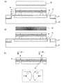
次に、基板11、下地膜12、素子層13、及び絶縁膜14に対して曲率を有する開口部(「切れ込み」または「穴」とも呼ぶ。)を形成する(図1(C))。曲率を有する開口部とは、開口部の深さに対して垂直に切断したときの断面積が変化する(好ましくは、連続的に変化する)ものをさす。例えば、図1(C)に示すように、開口部の深さが深くなるほど断面積が小さくなるように開口部を形成することが好ましい。また、開口部は、素子層13を構成する薄膜トランジスタ等を避けた領域や、基板11の端面に設けるようにする。本発明においては、後の基板11の研削、研磨工程を行う前に、基板11の一方の面側の一部に曲率を有する開口部を形成することが重要である。研削、研磨した後の基板は、基板が薄型化されているためその加工が困難であるが、本発明は研削、研磨する前に基板の一方の面側に曲率を有する開口部(穴)を形成するため、基板の端面に容易に曲率をつけることができる。
Next, an opening (also referred to as “cut” or “hole”) having a curvature is formed in the
開口部を形成する方法としては、レーザー光(例えば、紫外線(UV)レーザー(波長が紫外領域のレーザー))を照射する方法を用いることができる。レーザー光の条件としては、特に限定されず、好ましくは下地膜12、素子層13、及び絶縁膜14に用いられた材料に対して吸収係数が大きいものを用いる。なお、図1(C)に示すような開口部が形成される手段であれば、レーザー光を照射する以外の方法を用いてもよい。
As a method of forming the opening, a method of irradiating a laser beam (for example, an ultraviolet (UV) laser (a laser having a wavelength in the ultraviolet region)) can be used. The laser light conditions are not particularly limited, and those having a large absorption coefficient with respect to the materials used for the
次に、物理的な手段を用いて基板11を薄くする。例えば、研削手段31により、基板11の他方の面を研削する(図2(A))。このとき、基板11の厚さとして100μm以下になるように研削する。一般的に、この研削工程では、基板11が固定されたステージ53と研削手段31の一方又は両方を回転させることで、基板11の他方の面を研削する。研削手段31とは、例えば、砥石に相当する。なお、本明細書において、「基板11の他方の面」とは、下地膜12や素子層13が設けられている側の面とは逆側の面であり、研削手段31により研削される側の面をいう。
Next, the
なお、本実施の形態では、研削工程において、図2(A)に示すような治具を用いて研削を行う。まず、絶縁膜14を覆うようにフィルム15を貼る。次に、フィルム15をフレーム51に接着させる。また、逆の順番でもよいが、好ましくはフィルム15に対する絶縁膜14の貼り付けとフレーム51の接着を同時に行うとよい。
In the present embodiment, in the grinding process, grinding is performed using a jig as shown in FIG. First, the
フィルム15は、基板11を研削、研磨する際に基板を固定するために用いているもので、後の工程でフィルム15と絶縁膜14とは分離される。このため、フィルム15として、通常の状態ではその接着力が強く、光を照射するとその接着力が弱くなる性質を有するフィルムを用いることが好ましく、具体的には、紫外光を照射するとその接着力が弱くなるUVテープを用いるとよい。すなわち、フィルム15としてUVテープを用いることで、後の工程でフィルム15と絶縁膜14とを容易に分離することができる。また、引っ張ると延伸する性質を有するフィルム(「エキスパンドフィルム」と呼ばれる。)を用いることも好ましい。例えば、フィルム15として塩化ビニル樹脂、シリコン樹脂などを用いるとよい。
The
次に、基板11が接着されたフィルム15を、吸着治具の上に設置する。このとき、フレーム51の一表面よりも、基板11の一方の面の方が高くなるようにフィルム15を設置する。吸着治具は、例えばポーラスチャック52とステージ53とから構成されている。また、ポーラスチャック52は、多孔質からなり、真空チャック機構を有する。その後は、先に述べたとおり研削手段31により、基板11の他方の面を研削する。以上の工程により、基板11の研削は終了する。
Next, the
次に、研削の工程で用いた吸着治具の上に、基板11が接着されたフィルム15を設置したまま、研磨手段32により、基板11の他方の面を研磨する(図2(B))。基板11の厚さとしては100μmより薄くなるように研磨すればよいが、好ましくは2μm以上50μm以下(さらに好ましくは4μm以上30μm以下)になるように研磨する。このように基板11を薄くする(例えば、研削、研磨する)ことにより、基板11は可撓性を有するようになり、基板11から素子層を剥離する方法を用いずに可撓性を有する半導体装置を作製することが可能となる。また、この研磨工程も上記の研削工程と同様に、基板11が固定されたステージ53と研磨手段32の一方又は両方を回転させることで、基板11の表面を研磨する。研磨手段32とは、例えば、研磨パッドに相当する。その後、必要に応じて研削、研磨工程により生じたごみを除去するために、洗浄を行う。また、洗浄した後に、乾燥する工程を行ってもよい。
Next, the other surface of the
次に、基板11の他方の面から、上述した開口部(穴)を形成した位置に対応する領域に対してレーザー光を照射することにより、集積回路同士の境界線(集積回路の間)を切断する。(図2(C))。このとき、基板11の切断面が曲率を有する形状となるように切断することが本発明においては重要であり、好ましくは図2(C)に示すように基板の端面が凸型になるようにすることでチッピングやクラックの発生を最大限に抑制することができる。なお、図2(C)に示す基板11の切断面の拡大図のように、基板11の切断面が曲率半径r1の中心C1を有するような構成を示しているが、図12に示すように、曲率を有する穴を形成する際の該穴の曲率半径r2の中心C2と、基板11の他方の面から前記穴を形成した位置に対応する領域に対してレーザー光を照射する際に形成される切断面の曲率半径r3の中心C3とが異なる構成としてもよい。また、素子層13に設けられた素子は切断せず、素子層13に設けられた絶縁膜を切断する。このようにして、素子層13(複数の集積回路を含む層)が集積回路各々に分離され、前記複数の集積回路のうち少なくとも一つを有する積層体16(以下、「集積回路を有する積層体16」と略記する。)が複数形成される。
Next, the boundary line between the integrated circuits (between the integrated circuits) is formed by irradiating the region corresponding to the position where the above-described opening (hole) is formed from the other surface of the
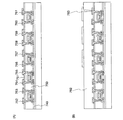
次に、集積回路を有する積層体16の間に隙間が形成されるように、フィルム15を延伸させる(図3(A))。この際、集積回路を有する積層体16それぞれの間の隙間を均等にするために、面方向に対して均等に引っ張るとよい。続いて、フィルム15に光を照射する(図3(B))。例えば、フィルム15がUVテープの場合は紫外光を照射する。フィルム15に光を照射することにより、フィルム15の接着力が弱くなり、フィルム15と集積回路を有する積層体16との間の密着性が小さくなる。そして、物理的手段により、集積回路を有する積層体16をフィルム15から分離することができる状態になる。
Next, the
なお、本明細書において物理的手段とは、物理学により認識される手段であり、具体的には力学の法則に当てはめることが可能な過程を有する力学的手段または機械的手段を指し、何らかの力学的エネルギー(機械的エネルギー)を変化させる手段を指している。つまり、物理的手段を用いて剥離するとは、例えば、ノズルから吹付けられるガスの風圧、超音波または楔状の部材を用いた負荷等を用いて外部から衝撃(ストレス)を与えることによって剥離することをいう。 In this specification, a physical means is a means recognized by physics, and specifically refers to a mechanical means or a mechanical means having a process that can be applied to the laws of mechanics. It refers to a means of changing the mechanical energy (mechanical energy). In other words, peeling using physical means means peeling by applying an impact (stress) from the outside using, for example, the wind pressure of a gas blown from a nozzle, a load using an ultrasonic wave or a wedge-shaped member, or the like. Say.
なお、上記の工程では、フィルム15を延伸させる工程の後に、フィルム15に光を照射する工程を行っているが、本発明はこの順番に制約されない。フィルム15に光を照射する工程の後に、フィルム15を延伸させる工程を行ってもよい。
In the above step, the step of irradiating the
次に、必要に応じて基体(フィルム)を用いて封止処理を行う。封止処理には2通りの方法がある。まず、1つ目の方法について説明する。 Next, sealing treatment is performed using a substrate (film) as necessary. There are two methods for the sealing process. First, the first method will be described.
1つ目の方法では、まず、ピックアップ手段21により、フィルム15から集積回路を有する積層体16を分離する。続いて、集積回路を有する積層体16の一方の面を第1の基体18に接着させるために、ピックアップ手段21により、集積回路を有する積層体16を第1の基体18上に設置する。
In the first method, first, the laminate 16 having an integrated circuit is separated from the
次に、集積回路を有する積層体16の他方の面を第2の基体19に接着させる(図3(C))。この工程は、ラミネート装置(貼り合わせ装置)を用いて行うものであり、当該ラミネート装置は、第2の基体19が巻き付いた供給ロール23と、加熱手段と加圧手段の一方又は両方を有するラミネートロール22とを有する。そして、ラミネートロール22と、供給ロール23とが順次回転することで、集積回路を有する積層体16のラミネート処理を連続的に行う。具体的には、ラミネートロール22により、集積回路を有する積層体16の他方の面を第2の基体19に接着させると共に、加熱処理又は加圧処理の一方又は両方を行って、集積回路を有する積層体16を第1の基体18と第2の基体19により封止する。
Next, the other surface of the stacked
封止に用いる第1の基体18、第2の基体19としては、帯電防止対策を施したフィルム(以下、「帯電防止フィルム」という。)、ポリプロピレン、ポリエステル、ビニル、ポリフッ化ビニル、塩化ビニルなどからなるフィルム、繊維質な材料からなる紙、基材フィルム(ポリエステル、ポリアミド、無機蒸着フィルム(酸化珪素やアルミナなどの無機材料が表面に蒸着されたフィルム)、紙類等)と接着性合成樹脂フィルム(アクリル系合成樹脂、エポキシ系合成樹脂等)との積層フィルム等を利用することができる。なお、帯電防止フィルムとしては、帯電防止可能な材料を樹脂中に分散させたフィルム、帯電防止可能な材料が貼り付けられたフィルム等が挙げられる。帯電防止可能な材料が貼り付けられたフィルムは、片面に帯電防止可能な材料を貼り付けられたフィルムであってもよいし、両面に帯電防止可能な材料を貼り付けられたフィルムであってもよい。また、片面に帯電防止可能な材料が貼り付けられたフィルムは、帯電防止可能な材料が貼り付けられた面をフィルムの内側になるように貼り付けてもよいし、フィルムの外側になるように貼り付けてもよい。また、帯電防止可能な材料はフィルムの全面、あるいは一部に貼り付けてあればよい。なお、帯電防止可能な材料としては、アルミなどの金属、インジウムと錫を含む酸化物(ITO)、両性界面活性剤の金属塩、イミダゾリン型両性界面活性剤、側鎖にカルボキシル基および4級アンモニウム塩基をもつ架橋性共重合体高分子を含む樹脂材料などが挙げられる。帯電防止フィルムを第1の基体18、第2の基体19として用いることで、外部からの静電気によって集積回路に悪影響が及ぶことを防止することができる。
As the
フィルムは、熱圧着(加熱処理と加圧処理)により、集積回路を有する積層体16に接着される。加熱処理と加圧処理を行う際には、フィルムの最表面に設けられた接着層か、または最外層に設けられた層(接着層ではない)を加熱処理によって溶かし、加圧により接着する。また、第1の基体18と第2の基体19の表面には接着層が設けられていてもよいし、接着層が設けられていなくてもよい。接着層は、熱硬化樹脂、紫外線硬化樹脂、エポキシ樹脂系接着剤、樹脂添加剤等の接着剤を含む層に相当する。また、封止後に内部への水分等の侵入を防ぐために封止するシート材にシリカコートを行うことが好ましく、例えば、接着層とポリエステル等のフィルムとシリカコートを積層させたシート材を利用することができる。
The film is bonded to the laminate 16 having an integrated circuit by thermocompression bonding (heat treatment and pressure treatment). When performing the heat treatment and the pressure treatment, the adhesive layer provided on the outermost surface of the film or the layer (not the adhesive layer) provided on the outermost layer is melted by the heat treatment and adhered by pressure. Further, an adhesive layer may be provided on the surfaces of the
以下には、上記のラミネート処理についてより詳しく説明する。ラミネートロール22と供給ロール23は、順次回転しており、供給ロール23は、ラミネートロール22に第2の基体19を供給する。また、複数の集積回路を有する積層体16が設けられた第1の基体18は、搬送手段24により順次搬送されている。ラミネート処理とは、集積回路を有する積層体16が接着された第1の基体18が、ラミネートロール22と搬送手段24との間を通過する際、ラミネートロール22と搬送手段24により、集積回路を有する積層体16と第1の基体18と第2の基体19に加圧処理と加熱処理の一方又は両方が行われる処理に相当する。ラミネート処理が行われると、集積回路を有する積層体16は、第1の基体18と第2の基体19により封止される。なお、搬送手段24は、ベルトコンベア、複数のローラー又はロボットアームに相当する。また、ラミネートロール22と搬送手段24により加熱処理が行われる場合、ラミネートロール22は、電熱線のヒータ又はオイル等に相当する加熱手段を有する。
Hereinafter, the laminating process will be described in more detail. The
次に、切断手段25により、第1の基体18と第2の基体19を切断する(図3(D))。切断手段25は、ダイサー、レーザー、ワイヤソーなどに相当する。以上の工程を経て、半導体装置17(チップ)が完成する。
Next, the
次に、2つ目の方法について説明する。 Next, the second method will be described.
まず、集積回路を有する積層体16の一方の面を覆うように、第1の基体18を設ける(図4(A))。次に、加熱手段26により、第1の基体18を加熱することにより、集積回路を有する積層体16の一方の面を第1の基体18に接着させる。続いて、フィルム15から集積回路を有する積層体16を分離するために、集積回路を有する積層体16が接着した第1の基体18とフィルム15とを分離する(図4(B))。
First, the
次に、集積回路を有する積層体16の他方の面を、第2の基体19に接着させて、集積回路を有する積層体16を第1の基体18と第2の基体19により封止する(図3(C))。続いて、第1の基体18と第2の基体19を切断する(図3(D))。これらの工程は、上記の1つ目の方法と同様に行えばよい。以上の工程を経て、半導体装置17(チップ)が完成する。
Next, the other surface of the
なお、上記の2つ目の方法によると、フィルム15に光を照射してから、集積回路を有する積層体16の一方の面を覆うように第1の基体18を設けている(図4(A))。しかしながら、本発明はこの順番に制約されず、集積回路を有する積層体16の一方の面を覆うように第1の基体18を設けて、当該第1の基体18を加熱した後に、フィルム15と集積回路を有する積層体16との間の密着性を小さくするために、フィルム15に光を照射してもよい。
According to the second method, the
本実施の形態では、第1の基体18、第2の基体19の2枚のフィルムを用いて集積回路を有する積層体16を封止したが、第1の基体18のみを用いて集積回路を有する積層体16を封止してもよい。これは、集積回路を有する積層体16における基板11それ自体が外部からの水分や不純物の混入を防止する役割を果たすからである。したがって、集積回路を有する積層体16における絶縁膜14(絶縁膜14を設けない構成とした場合は、素子層13)の表面を第1の基体18で覆う構成としてもよい。
In this embodiment, the laminate 16 having an integrated circuit is sealed using two films of the
以上のように、基板上に素子層を形成した後に、基板を薄型化(例えば、研削、研磨)して基板の厚さを2μm以上50μm以下、好ましくは4μm以上30μm以下とし、且つ基板の端面が曲率を有するように形成することによって、信頼性の高い半導体装置を作製することができる。また、複数の集積回路を含む層を個々の集積回路に分断すると同時に基板の端面に曲率を付けるようにしているため、新たに工程を増やすことなく信頼性の高い半導体装置を作製することができる。 As described above, after the element layer is formed on the substrate, the substrate is thinned (for example, ground or polished) so that the thickness of the substrate is 2 μm or more and 50 μm or less, preferably 4 μm or more and 30 μm or less. By forming so that has a curvature, a highly reliable semiconductor device can be manufactured. In addition, since a layer including a plurality of integrated circuits is divided into individual integrated circuits and at the same time a curvature is given to the end surface of the substrate, a highly reliable semiconductor device can be manufactured without increasing the number of steps. .
(実施の形態2)
本実施の形態では、薄膜トランジスタ及びアンテナを含む本発明の半導体装置の作製方法について、図面を参照して説明する。特に、素子層の構造について詳細に説明する。
(Embodiment 2)
In this embodiment, a method for manufacturing a semiconductor device of the present invention including a thin film transistor and an antenna will be described with reference to drawings. In particular, the structure of the element layer will be described in detail.
まず、基板701上に下地膜703を形成する(図5(A))。基板701、下地膜703の材料や形成方法については実施の形態1で説明したものを用いることができるので、ここでは説明を省略する。
First, a
次に、下地膜703上に、非晶質半導体膜704(例えば、非晶質珪素を主成分とする膜)を形成する。非晶質半導体膜704は、スパッタ法やプラズマCVD法等の各種CVD法により、25〜200nm(好ましくは30〜150nm)の厚さで形成する。続いて、非晶質半導体膜704を結晶化して、結晶質半導体膜を形成する。結晶化の方法としては、レーザー結晶化法、RTAまたはファーネスアニール炉を用いる熱結晶化法、結晶化を助長する金属元素を用いる熱結晶化法、結晶化を助長する金属元素を用いる熱結晶化法とレーザー結晶化法を組み合わせた方法等を用いることができる。その後、得られた結晶質半導体膜をパターニングして、結晶質半導体膜706〜710を形成する(図5(B))。なお、下地膜703及び非晶質半導体膜704は、大気に曝さずに連続して形成することもできる。なお、本明細書において「パターニング」とは、所望の形状にエッチングすることを指すものとする。
Next, an amorphous semiconductor film 704 (eg, a film containing amorphous silicon as a main component) is formed over the
結晶質半導体膜706〜710の作製工程の一例を以下に簡単に説明する。非晶質半導体膜を結晶化する方法としては、レーザー結晶化法、RTAまたはファーネスアニール炉を用いる熱結晶化法、結晶化を助長する金属元素を用いる熱結晶化法、結晶化を助長する金属元素を用いる熱結晶化法とレーザー結晶化法とを組み合わせた方法等が挙げられる。また、他の結晶化の方法として、DCバイアスを印加して熱プラズマを発生させ、当該熱プラズマを半導体膜に作用させることにより結晶化を行ってもよい。
An example of a manufacturing process of the
本実施の形態では、プラズマCVD法により膜厚40〜300nmの非晶質半導体膜を形成した後、加熱処理により非晶質半導体膜を結晶化して結晶質半導体膜706〜710を形成する。加熱処理としては、レーザー加熱炉、レーザー照射、若しくはレーザー光の代わりにランプから発する光の照射(以下、ランプアニールと表記する)、又はこれらを組み合わせて用いることができる。
In this embodiment, after an amorphous semiconductor film with a thickness of 40 to 300 nm is formed by a plasma CVD method, the amorphous semiconductor film is crystallized by heat treatment to form
レーザー照射を用いる場合、連続発振型のレーザー光(CWレーザー光)やパルス発振型のレーザー光(パルスレーザー光)を用いることができる。使用可能なレーザー光としては、Arレーザー、Krレーザー、エキシマレーザーなどの気体レーザー、単結晶のYAG、YVO4、フォルステライト(Mg2SiO4)、YAlO3、GdVO4、もしくは多結晶(セラミック)のYAG、Y2O3、YVO4、YAlO3、GdVO4に、ドーパントとしてNd、Yb、Cr、Ti、Ho、Er、Tm、Taのうち1種もしくは複数種添加されているものを媒質とするレーザー、ガラスレーザー、ルビーレーザー、アレキサンドライトレーザー、Ti:サファイアレーザー、銅蒸気レーザー、金蒸気レーザーのうち、一種または複数種から発振されるものを用いることができる。このようなレーザー光の基本波、及びこれらの基本波の第2高調波から第4高調波のレーザー光を照射することで、大粒径の結晶を得ることができる。例えば、Nd:YVO4レーザー(基本波1064nm)の第2高調波(532nm)や第3高調波(355nm)を用いることができる。このときレーザーのエネルギー密度は0.01〜100MW/cm2程度(好ましくは0.1〜10MW/cm2)が必要である。そして、走査速度を10〜2000cm/sec程度として照射する。 When laser irradiation is used, continuous wave laser light (CW laser light) or pulsed laser light (pulse laser light) can be used. Usable laser beams include gas lasers such as Ar laser, Kr laser, and excimer laser, single crystal YAG, YVO 4 , forsterite (Mg 2 SiO 4 ), YAlO 3 , GdVO 4 , or polycrystalline (ceramic) YAG, Y 2 O 3 , YVO 4 , YAlO 3 , GdVO 4 of Nd, Yb, Cr, Ti, Ho, Er, Tm, Ta as dopants are added as a medium. Lasers, glass lasers, ruby lasers, alexandrite lasers, Ti: sapphire lasers, copper vapor lasers, and gold vapor lasers that oscillate from one or more types can be used. By irradiating the fundamental wave of such laser light and the second to fourth harmonics of these fundamental waves, a crystal having a large grain size can be obtained. For example, the second harmonic (532 nm) or the third harmonic (355 nm) of an Nd: YVO 4 laser (fundamental wave 1064 nm) can be used. Energy density of the laser is about 0.01 to 100 MW / cm 2 (preferably 0.1 to 10 MW / cm 2) is required. Then, irradiation is performed at a scanning speed of about 10 to 2000 cm / sec.
なお、単結晶のYAG、YVO4、フォルステライト(Mg2SiO4)、YAlO3、GdVO4、若しくは多結晶(セラミック)のYAG、Y2O3、YVO4、YAlO3、GdVO4に、ドーパントとしてNd、Yb、Cr、Ti、Ho、Er、Tm、Taのうち1種または複数種添加されているものを媒質とするレーザー、Arイオンレーザー、Ti:サファイアレーザーは、それぞれ連続発振をさせることが可能であり、Qスイッチ動作やモード同期などを行うことによって10MHz以上の発振周波数でパルス発振をさせることも可能である。10MHz以上の発振周波数でレーザー光を発振させると、半導体膜がレーザーによって溶融してから固化するまでの間に、次のパルスが半導体膜に照射される。従って、発振周波数が低いパルスレーザーを用いる場合と異なり、半導体膜中において固液界面を連続的に移動させることができるため、走査方向に向かって連続的に成長した結晶粒を得ることができる。 Note that single crystal YAG, YVO 4 , forsterite (Mg 2 SiO 4 ), YAlO 3 , GdVO 4 , or polycrystalline (ceramic) YAG, Y 2 O 3 , YVO 4 , YAlO 3 , GdVO 4 , dopants Nd, Yb, Cr, Ti, Ho, Er, Tm, Ta, one or more added lasers, Ar ion lasers, and Ti: sapphire lasers that are continuously oscillated. It is also possible to perform pulse oscillation at an oscillation frequency of 10 MHz or more by performing Q switch operation, mode synchronization, or the like. When laser light is oscillated at an oscillation frequency of 10 MHz or more, the semiconductor film is irradiated with the next pulse during the period from when the semiconductor film is melted by the laser to solidification. Therefore, unlike the case of using a pulse laser having a low oscillation frequency, the solid-liquid interface can be continuously moved in the semiconductor film, so that crystal grains continuously grown in the scanning direction can be obtained.
上述した連続発振レーザーまたは10MHz以上の周波数で発振するレーザー光を用いて結晶化する場合、結晶化された半導体膜の表面を平坦なものとすることができる。この結果、後に形成するゲート絶縁膜705を薄膜化することも可能であり、また、ゲート絶縁膜の耐圧を向上させることに寄与することができる。
In the case of crystallization using the above-described continuous wave laser or laser light oscillated at a frequency of 10 MHz or more, the surface of the crystallized semiconductor film can be made flat. As a result, it is possible to reduce the thickness of the
また、媒質としてセラミック(多結晶)を用いると、短時間かつ低コストで自由な形状に媒質を形成することが可能である。単結晶を用いる場合、通常、直径数mm、長さ数十mmの円柱状の媒質が用いられているが、セラミックを用いる場合はさらに大きいものを作ることが可能である。 In addition, when ceramic (polycrystal) is used as a medium, it is possible to form the medium in a free shape in a short time and at low cost. When a single crystal is used, a cylindrical medium having a diameter of several millimeters and a length of several tens of millimeters is usually used. However, when ceramic is used, a larger one can be made.
発光に直接寄与する媒質中のNd、Ybなどのドーパントの濃度は、単結晶中でも多結晶中でも大きく変えることは困難なため、ドーパントの濃度を増加させることによるレーザーの出力向上にはある程度限界がある。しかしながら、セラミックの場合、単結晶と比較して媒質の大きさを著しく大きくすることができるため大幅な出力向上が期待できる。 Since it is difficult to change the concentration of dopants such as Nd and Yb in the medium that directly contributes to light emission, whether it is single crystal or polycrystal, there is a certain limit to improving the laser output by increasing the dopant concentration. . However, in the case of ceramic, since the size of the medium can be remarkably increased as compared with the single crystal, a great improvement in output can be expected.
さらに、セラミックの場合では、平行六面体形状や直方体形状の媒質を容易に形成することが可能である。このような形状の媒質を用いて、発振光を媒質の内部でジグザグに進行させると、発振光路を長くとることができる。そのため、増幅が大きくなり、大出力で発振させることが可能になる。また、このような形状の媒質から射出されるレーザー光は射出時の断面形状が四角形状であるため、丸状のビームと比較すると、線状ビームに整形するのに有利である。このように射出されたレーザー光を、光学系を用いて整形することによって、短辺の長さ1mm以下、長辺の長さ数mm〜数mの線状ビームを容易に得ることが可能となる。また、励起光を媒質に均一に照射することにより、線状ビームは長辺方向にエネルギー分布の均一なものとなる。 Further, in the case of ceramic, a medium having a parallelepiped shape or a rectangular parallelepiped shape can be easily formed. When a medium having such a shape is used to cause oscillation light to travel in a zigzag manner inside the medium, the oscillation optical path can be made longer. As a result, amplification is increased and oscillation can be performed with high output. Further, since the laser light emitted from the medium having such a shape has a quadrangular cross-sectional shape at the time of emission, it is advantageous for shaping into a linear beam as compared with a round beam. By shaping the emitted laser light by using an optical system, it is possible to easily obtain a linear beam having a short side length of 1 mm or less and a long side length of several mm to several m. Become. In addition, by irradiating the medium with the excitation light uniformly, the linear beam has a uniform energy distribution in the long side direction.
この線状ビームを半導体膜に照射することによって、半導体膜をより均一にアニールすることが可能になる。線状ビームの両端まで均一なアニールが必要な場合は、その両端にスリットを配置し、エネルギーの減衰部を遮光するなどの工夫をすればよい。 By irradiating the semiconductor film with this linear beam, the semiconductor film can be annealed more uniformly. If uniform annealing is required up to both ends of the linear beam, it is sufficient to arrange a slit at both ends to shield the energy attenuation portion.
このようにして得られた強度が均一な線状ビームを用いて半導体膜をアニールし、この半導体膜を用いて半導体装置を作製すると、その半導体装置の特性を、良好かつ均一なものとすることができる。 When a semiconductor film is annealed using a linear beam having a uniform intensity obtained in this way and a semiconductor device is manufactured using this semiconductor film, the characteristics of the semiconductor device are made good and uniform. Can do.
結晶化を助長する金属元素を用いる熱結晶化法として、具体的な方法の一例を挙げる。結晶化を助長する金属元素であるニッケルを含む溶液を非晶質半導体膜上に保持させた後、非晶質半導体膜に脱水素化の処理(500℃、1時間)と、熱結晶化の処理(550℃、4時間)を行って結晶質半導体膜を形成する。その後、必要に応じてレーザー光を照射し、フォトリソグラフィ法を用いたパターニング処理によって結晶質半導体膜706〜710を形成すればよい。
An example of a specific method is given as a thermal crystallization method using a metal element that promotes crystallization. After a solution containing nickel, which is a metal element that promotes crystallization, is held on the amorphous semiconductor film, the amorphous semiconductor film is subjected to dehydrogenation treatment (500 ° C., 1 hour), and thermal crystallization. Processing (550 ° C., 4 hours) is performed to form a crystalline semiconductor film. Thereafter, laser light may be irradiated as necessary, and the
結晶化を助長する金属元素を用いる熱結晶化法は、低温且つ短時間で非晶質半導体膜の結晶化が可能となるうえ、結晶の方向が揃うという利点がある一方、金属元素が結晶質半導体膜に残存するためにオフ電流が上昇し、特性が安定しないという欠点がある。そこで、結晶質半導体膜上に、ゲッタリングサイトとして機能する非晶質半導体膜を形成するとよい。ゲッタリングサイトとなる非晶質半導体膜には、リンやアルゴンの不純物元素を含有させる必要があるため、好適には、アルゴンを高濃度に含有させることが可能なスパッタ法で形成するとよい。その後、加熱処理(RTA法やファーネスアニール炉を用いた熱アニール等)を行って、非晶質半導体膜中に金属元素を拡散させ、続いて、当該金属元素を含む非晶質半導体膜を除去する。このようなゲッタリングプロセスを行うことにより、結晶質半導体膜中の金属元素の含有量を低減または除去することができる。 The thermal crystallization method using a metal element that promotes crystallization is advantageous in that the amorphous semiconductor film can be crystallized at a low temperature in a short time and the crystal orientation is aligned. Since it remains in the semiconductor film, the off-current increases and the characteristics are not stable. Therefore, an amorphous semiconductor film functioning as a gettering site is preferably formed over the crystalline semiconductor film. Since the amorphous semiconductor film serving as a gettering site needs to contain an impurity element such as phosphorus or argon, it is preferably formed by a sputtering method which can contain argon at a high concentration. Then, heat treatment (RTA method or thermal annealing using a furnace annealing furnace) is performed to diffuse the metal element in the amorphous semiconductor film, and then the amorphous semiconductor film containing the metal element is removed. To do. By performing such a gettering process, the content of the metal element in the crystalline semiconductor film can be reduced or removed.
次に、結晶質半導体膜706〜710を覆うゲート絶縁膜705を形成する。ゲート絶縁膜705は、スパッタ法やプラズマCVD法等の各種CVD法により形成すればよい。具体的には、酸化珪素膜(SiOx膜)、窒化珪素膜(SiNx膜)、窒素を含む酸化珪素膜(SiOxNy膜)(x>y)(x、yは正の整数)、酸素を含む窒化珪素膜(SiNxOy膜)(x>y)(x、yは正の整数)を、単層構造として形成するか、当該これらの膜を適宜積層して形成する。また、結晶質半導体膜706〜710に対して酸素、窒素、または酸素及び窒素を含む雰囲気中で高密度プラズマ処理を行うことにより、結晶質半導体膜706〜710の表面を酸化または窒化し、ゲート絶縁膜を形成してもよい。高密度プラズマ処理により形成されたゲート絶縁膜は、CVD法やスパッタ法等により形成された膜と比較して膜厚や膜質などの均一性に優れ、且つ緻密な膜を形成することができる。
Next, a
本明細書において「高密度プラズマ処理」とは、プラズマの電子密度が1×1011cm−3以上1×1013cm−3以下であり、プラズマの電子温度が0.5eV以上1.5eV以下であることを特徴としている。以後、本明細書において単に「高密度プラズマ処理」と記載している場合、上述の条件下でプラズマ処理を行っているものとする。プラズマの電子密度が高密度でありながら、基板上に形成された被処理物(金属膜)付近での電子温度が低いため、基板に対するプラズマ損傷を防止することができる。また、プラズマの電子密度が1×1011cm−3以上と高密度であるため、酸化(または窒化)処理によって形成される酸化物(または窒化物)の膜厚均一性に優れ、且つ緻密な膜を形成することができる。また、プラズマの電子温度が1.5eV以下と低いため、プラズマ処理や熱酸化法と比較して低温度で酸化処理(または窒化処理)を行うことができる。たとえば、ガラス基板の歪点温度よりも100度以上低い温度(代表的には、250〜550℃)でプラズマ処理を行っても十分にプラズマ酸化処理(またはプラズマ窒化処理)を行うことができる。なお、プラズマを形成するための電源周波数はマイクロ波(2.45GHz)を用いている。また、プラズマの電位は5V以下と低電位であり、原料分子の過剰解離を抑制することができる。 In this specification, “high density plasma treatment” means that the electron density of plasma is 1 × 10 11 cm −3 or more and 1 × 10 13 cm −3 or less, and the electron temperature of plasma is 0.5 eV or more and 1.5 eV or less. It is characterized by being. Hereinafter, in the present specification, when simply described as “high-density plasma treatment”, the plasma treatment is performed under the above-described conditions. Although the electron density of the plasma is high, the electron temperature in the vicinity of the object to be processed (metal film) formed on the substrate is low, so that plasma damage to the substrate can be prevented. Further, since the electron density of plasma is as high as 1 × 10 11 cm −3 or more, the film thickness uniformity of oxide (or nitride) formed by oxidation (or nitriding) treatment is excellent and dense. A film can be formed. In addition, since the electron temperature of plasma is as low as 1.5 eV or less, oxidation treatment (or nitridation treatment) can be performed at a lower temperature than plasma treatment or thermal oxidation. For example, plasma oxidation treatment (or plasma nitridation treatment) can be sufficiently performed even if the plasma treatment is performed at a temperature lower than the strain point temperature of the glass substrate by 100 degrees or more (typically 250 to 550 ° C.). Note that a microwave (2.45 GHz) is used as a power supply frequency for forming plasma. Further, the plasma potential is as low as 5 V or less, and excessive dissociation of source molecules can be suppressed.
酸素を含む雰囲気としては、酸素(O2)、二酸化窒素(NO2)、もしくは一酸化二窒素(N2O)と、希ガスとの混合ガス、または、酸素(O2)、二酸化窒素(NO2)もしくは一酸化二窒素(N2O)と、希ガスと、水素(H2)との混合ガスを用いることができる。希ガスとしては、アルゴン(Ar)、キセノン(Xe)、クリプトン(Kr)が挙げられる。混合ガス中の各ガスの流量比(または圧力比)は、適宜決定すればよい。混合ガスの組み合わせの一例としては、酸素(または二酸化窒素や一酸化二窒素)を0.1〜100sccm、アルゴンを100〜5000sccmとすればよい。また、混合ガスの組み合わせの他の一例としては、酸素(または二酸化窒素や一酸化二窒素)を0.1〜100sccm、水素を0.1〜100sccm、アルゴンを100〜5000sccmとすればよく、酸素(または二酸化窒素や一酸化二窒素):水素:アルゴン=1:1:100の比率で混合ガスを導入することが好ましい。例えば、酸素(または二酸化窒素や一酸化二窒素)を5sccm、水素を5sccm、アルゴンを500sccmとして混合ガスを導入すればよい。混合ガス中に水素を導入しておくことで、酸化の処理時間を短縮することができる。 As an atmosphere containing oxygen, oxygen (O 2 ), nitrogen dioxide (NO 2 ), a mixed gas of dinitrogen monoxide (N 2 O) and a rare gas, or oxygen (O 2 ) and nitrogen dioxide ( A mixed gas of NO 2 ) or dinitrogen monoxide (N 2 O), a rare gas, and hydrogen (H 2 ) can be used. Examples of the rare gas include argon (Ar), xenon (Xe), and krypton (Kr). What is necessary is just to determine suitably the flow ratio (or pressure ratio) of each gas in mixed gas. As an example of the combination of mixed gases, oxygen (or nitrogen dioxide or dinitrogen monoxide) may be 0.1 to 100 sccm, and argon may be 100 to 5000 sccm. As another example of the combination of mixed gases, oxygen (or nitrogen dioxide or dinitrogen monoxide) may be 0.1 to 100 sccm, hydrogen may be 0.1 to 100 sccm, and argon may be 100 to 5000 sccm. (Or nitrogen dioxide or dinitrogen monoxide): It is preferable to introduce the mixed gas at a ratio of hydrogen: argon = 1: 1: 100. For example, the mixed gas may be introduced with oxygen (or nitrogen dioxide or dinitrogen monoxide) at 5 sccm, hydrogen at 5 sccm, and argon at 500 sccm. By introducing hydrogen into the mixed gas, the oxidation treatment time can be shortened.
窒素を含む雰囲気としては、窒素(N2)もしくはアンモニア(NH3)と、希ガスとの混合ガス、または、窒素(N2)もしくはアンモニア(NH3)と、希ガスと、水素(H2)との混合ガスを用いることができる。混合ガスの組み合わせの一例としては、窒素(またはアンモニア)を20〜2000sccm、アルゴンを100〜10000sccmとすればよい。また、混合ガスの組み合わせの他の一例としては、窒素(またはアンモニア)を20〜2000sccm、水素を1〜500sccm、アルゴンを100〜10000sccmとすればよく、窒素(またはアンモニア):水素:アルゴン=20:1:100の比率で混合ガスを導入することが好ましい。例えば、窒素(またはアンモニア)を100sccm、水素を5sccm、アルゴンを500sccmとして混合ガスを導入すればよい。混合ガス中に水素を導入しておくことで、窒化の処理時間を短縮することができる。 As the atmosphere containing nitrogen, nitrogen (N 2) or ammonia (NH 3), a mixed gas of a rare gas or a nitrogen (N 2) or ammonia (NH 3), and a rare gas, hydrogen (H 2 ) And a mixed gas can be used. As an example of a combination of mixed gases, nitrogen (or ammonia) may be 20 to 2000 sccm, and argon may be 100 to 10,000 sccm. As another example of the combination of the mixed gases, nitrogen (or ammonia) may be 20 to 2000 sccm, hydrogen may be 1 to 500 sccm, and argon may be 100 to 10,000 sccm. Nitrogen (or ammonia): hydrogen: argon = 20 It is preferable to introduce the mixed gas at a ratio of 1: 100. For example, the mixed gas may be introduced with nitrogen (or ammonia) as 100 sccm, hydrogen as 5 sccm, and argon as 500 sccm. By introducing hydrogen into the mixed gas, the nitriding treatment time can be shortened.
酸素及び窒素を含む雰囲気としては、N2またはNH3と、O2と、希ガスとの混合ガスを用いることができる。混合ガスの組み合わせの一例としては、窒素(またはアンモニア)を20〜1000sccm、酸素を10〜500sccm、アルゴンを100〜5000sccmとすればよく、窒素(またはアンモニア):酸素:アルゴン=2:1:10の比率で混合ガスを導入することが好ましい。 As an atmosphere containing oxygen and nitrogen, a mixed gas of N 2 or NH 3 , O 2, and a rare gas can be used. As an example of the mixed gas combination, nitrogen (or ammonia) may be 20 to 1000 sccm, oxygen may be 10 to 500 sccm, and argon may be 100 to 5000 sccm. Nitrogen (or ammonia): oxygen: argon = 2: 1: 10 It is preferable to introduce the mixed gas at a ratio of
高密度プラズマ処理を行ってゲート絶縁膜705を形成する場合、1〜20nm、代表的には5〜10nmの絶縁膜が結晶質半導体膜706〜710に形成される。この場合の反応は固相反応であるため、当該絶縁膜と結晶質半導体膜706〜710との界面準位密度をきわめて低くすることができる。また、結晶質半導体膜706〜710を直接酸化または窒化するため、形成されるゲート絶縁膜705の厚さを、理想的にはばらつきをきわめて小さくすることができる。さらに、結晶性シリコンの結晶粒界でも強い酸化がおこらないため、非常に好ましい状態となる。すなわち、ここで示す高密度プラズマ処理で半導体膜の表面を固相酸化することにより、結晶粒界において異常に酸化反応をさせることなく、且つ、均一性が良く、界面準位密度が低い絶縁膜を形成することができる。
In the case where the
なお、ゲート絶縁膜705は、高密度プラズマ処理によって形成される絶縁膜のみを用いても良いし、それに加えてプラズマや熱反応を利用したCVD法により酸化珪素、酸素を含む窒化珪素、窒素を含む酸化珪素などの絶縁膜を堆積し、積層させても良い。いずれにしても、高密度プラズマで形成した絶縁膜をゲート絶縁膜の一部又は全部に含んで形成されるトランジスタは、特性のばらつきを小さくすることができる。
Note that the
また、非晶質半導体膜704に対し、連続発振レーザーまたは10MHz以上の周波数で発振するレーザー光を照射しながら一方向に走査して結晶化した結晶質半導体膜706〜710は、そのビームの走査方向に結晶が成長する特性がある。したがって、走査方向をチャネル長方向(チャネル形成領域が形成されたときにキャリアが流れる方向)に合わせてトランジスタを配置し、高密度プラズマ処理によって形成されたゲート絶縁膜705を組み合わせることで、特性ばらつきがより小さく、しかも電界効果移動度が高いトランジスタを得ることができる。
Further, the
次に、ゲート絶縁膜705上に、第1の導電膜と第2の導電膜とを積層して形成する。第1の導電膜及び第2の導電膜は、それぞれスパッタ法やプラズマCVD法等の各種CVD法により形成すればよい。本実施の形態では、第1の導電膜を20〜100nmの厚さに形成し、第2の導電膜を100〜400nmの厚さに形成する。また、第1の導電膜と第2の導電膜は、タンタル(Ta)、タングステン(W)、チタン(Ti)、モリブデン(Mo)、アルミニウム(Al)、銅(Cu)、クロム(Cr)、ニオブ(Nb)等から選択された元素またはこれらの元素を主成分とする合金材料若しくは化合物材料を用いて形成することができる。また、リン等の不純物元素をドーピングした多結晶珪素に代表される半導体材料により形成することもできる。第1の導電膜と第2の導電膜の組み合わせの例としては、窒化タンタル(TaN)膜とタングステン(W)膜、窒化タングステン(WN)膜とタングステン膜、窒化モリブデン(MoN)膜とモリブデン(Mo)膜等が挙げられる。タングステンや窒化タンタルは、耐熱性が高いため、第1の導電膜と第2の導電膜を形成した後に、熱活性化を目的とした加熱処理を行うことができる。また、第1の導電膜と第2の導電膜による2層構造ではなく、単層構造としてもよいし、3層構造とすることもできる。単層構造や3層構造にする場合、導電膜の材料として、上述した第1の導電膜、第2の導電膜と同様のものを自由に選択することが可能である。
Next, a first conductive film and a second conductive film are stacked over the
次に、フォトリソグラフィ法を用いてレジストからなるマスクを形成し、ゲート電極とゲート線を形成するためのエッチング処理を行って、ゲート電極として機能する導電膜716〜725(以下、本明細書において「ゲート電極」とよぶことがある。)を形成する。
Next, a resist mask is formed using a photolithography method, and etching treatment for forming a gate electrode and a gate line is performed, so that
次に、フォトリソグラフィ法により、レジストからなるマスクを形成した後、結晶質半導体膜706、708〜710に、イオンドープ法またはイオン注入法により、N型を付与する不純物元素を低濃度に添加する。このようにして、N型不純物領域711、713〜715及びチャネル形成領域780、782〜784が形成される。N型を付与する不純物元素は、15族に属する元素を用いればよく、例えばリン(P)、砒素(As)を用いる。
Next, after forming a resist mask by photolithography, an impurity element imparting N-type is added to the
次に、フォトリソグラフィ法によりレジストからなるマスクを形成して、結晶質半導体膜707に、P型を付与する不純物元素を添加して、P型不純物領域712とチャネル形成領域781を形成する。P型を付与する不純物元素は、例えばボロン(B)を用いる。なお、N型不純物領域711、713〜715及びP型不純物領域712を形成する順番は、本実施の形態のようにN型不純物領域711、713〜715を形成した後にP型不純物領域712を形成してもよいし、P型不純物領域712を形成した後にN型不純物領域711、713〜715を形成してもよい。
Next, a resist mask is formed by photolithography, and an impurity element imparting P-type conductivity is added to the
次に、ゲート絶縁膜705と導電膜716〜725を覆うように、絶縁膜を形成する。絶縁膜は、スパッタ法やプラズマCVD法等の各種CVD法により、珪素、珪素の酸化物、または珪素の窒化物など無機材料からなる膜や、有機樹脂などの有機材料からなる膜を、単層または積層して形成する。次に、絶縁膜を、垂直方向を主体とした異方性エッチングにより選択的にエッチングして、導電膜716〜725の側面に接する絶縁膜(サイドウォールともよばれる)739〜743を形成する(図5(C))。また、絶縁膜739〜743の作製と同時に、ゲート絶縁膜705がエッチングされて形成された絶縁膜734〜738を形成する。絶縁膜739〜743は、後にLDD(Lightly Doped drain)領域を形成する際のドーピング用のマスクとして用いる。
Next, an insulating film is formed so as to cover the
次に、フォトリソグラフィ法により形成したレジストからなるマスクと、絶縁膜739〜743をマスクとして用いて、結晶質半導体膜706、708〜710にN型を付与する不純物元素を添加して、第1のN型不純物領域(LDD領域ともよぶ)727、729、731、733と、第2のN型不純物領域726、728、730、732とを形成する。第1のN型不純物領域727、729、731、733が含む不純物元素の濃度は、第2のN型不純物領域726、728、730、732の不純物元素の濃度よりも低い。上記工程を経て、N型の薄膜トランジスタ744、746〜748と、P型の薄膜トランジスタ745が完成する。
Next, an impurity element imparting n-type conductivity is added to the
なお、LDD領域を形成するためには、ゲート電極を2層以上の積層構造として、当該ゲート電極にテーパーがつくようなエッチングや異方性エッチングを行って、当該ゲート電極を構成する下層の導電膜をマスクとして用いる手法と、サイドウォールの絶縁膜をマスクとして用いる手法がある。前者の手法を採用して形成された薄膜トランジスタは、ゲート絶縁膜を介してLDD領域をゲート電極と重ねて配置させた構造となっているが、この構造は、ゲート電極にテーパーがつくようなエッチングや異方性エッチングを利用するために、LDD領域の幅を制御することが難しく、エッチング工程が良好に行われなければ、LDD領域を形成することが出来ない場合がある。一方、後者のサイドウォールの絶縁膜をマスクとして用いる手法は、前者の手法と比較すると、LDD領域の幅の制御が容易であり、また、LDD領域を確実に形成することができる。なお、「ゲート電極にテーパーがつくようなエッチング」とは、ゲート電極の側面がテーパー状になるようなエッチングのことをいう。 In order to form the LDD region, the gate electrode has a stacked structure of two or more layers, and the gate electrode is tapered and anisotropic etching is performed to form a conductive layer under the gate electrode. There are a method using a film as a mask and a method using an insulating film on a sidewall as a mask. The thin film transistor formed by using the former method has a structure in which the LDD region is disposed so as to overlap the gate electrode through the gate insulating film. This structure is etched so that the gate electrode is tapered. In addition, since the anisotropic etching is used, it is difficult to control the width of the LDD region, and the LDD region may not be formed unless the etching process is performed well. On the other hand, the latter method using the sidewall insulating film as a mask makes it easier to control the width of the LDD region than the former method, and the LDD region can be formed reliably. Note that “etching in which the gate electrode is tapered” refers to etching in which the side surface of the gate electrode is tapered.
なお、露出されたN型不純物領域726、728、730、732、及びP型不純物領域712の表面に形成された自然酸化膜を除去した後、金属膜を用いてシリサイド領域をそれぞれ適宜形成してもよい。金属膜としては、ニッケル膜、チタン膜、コバルト膜、白金膜、もしくはこれら元素のうち少なくとも2種類を含む合金でなる膜等を使用することができる。より具体的には、金属膜として例えばニッケル膜を用い、室温の下、成膜電力500W〜1kWでニッケル膜をスパッタ法により成膜した後、加熱処理によってシリサイド領域を形成する。加熱処理はRTAやファーネスアニール等を用いることができる。このとき、金属膜の膜厚、加熱温度、加熱時間を制御することにより、N型不純物領域726、728、730、732、及びP型不純物領域712の表面のみをシリサイド領域にすることもできるし、全体をシリサイド領域とすることもできる。最後に、未反応のニッケルを除去する。例えば、HCl:HNO3:H2O=3:2:1からなるエッチング溶液を用いて未反応のニッケルを除去する。
After removing the natural oxide film formed on the exposed N-
なお、本実施の形態では、薄膜トランジスタ744〜748をトップゲート型とした例を説明したが、それぞれボトムゲート型の薄膜トランジスタとしてもよいことはいうまでもない。また、薄膜トランジスタ744〜748のチャネル形成領域が、各々一つ形成されるシングルゲート構造について説明したが、チャネル形成領域が二つ形成されるダブルゲート構造または三つ形成されるトリプルゲート構造であってもよい。あるいは、チャネル形成領域の上下にゲート絶縁膜を介して配置された2つのゲート電極を有するデュアルゲート型やその他の構造としてもよい。
Note that although an example in which the
また、薄膜トランジスタ744〜748を構成する半導体膜の構造は、それぞれ本実施の形態で説明した構成以外のものとしてもよく、例えば不純物領域(ソース領域、ドレイン領域、LDD領域を含む)をそれぞれ形成してもよいし、Pチャネル型、Nチャネル型またはCMOS回路を形成してもよい。また、半導体膜の上方または下方に設けられるゲート電極の側面と接するように絶縁膜(サイドウォール)を形成してもよい。
The structure of the semiconductor film included in the
上記工程を経て、N型の薄膜トランジスタ744、746〜748と、P型の薄膜トランジスタ745を完成させた後、半導体膜の結晶性の回復や半導体膜に添加された不純物元素の活性化を目的とする加熱処理を行ってもよい。また、好ましくは加熱処理を行った後、露出されているゲート絶縁膜705に対して水素を含む雰囲気中で高密度プラズマ処理を行うことにより、当該ゲート絶縁膜705の表面に水素を含有させるようにしてもよい。これは、後の半導体膜の水素化の工程を行う際に、この水素を利用することができるためである。または、基板に対して350〜450℃の加熱をしながら水素を含む雰囲気中で高密度プラズマ処理を行うことで、半導体膜の水素化を行うことができる。なお、水素を含む雰囲気としては、水素(H2)またはアンモニア(NH3)と、希ガス(例えば、アルゴン(Ar))とを混合したガスを用いることができる。水素を含む雰囲気として、アンモニア(NH3)と希ガス(例えば、アルゴン(Ar))との混合ガスを用いた場合、ゲート絶縁膜705表面の水素化と同時に表面を窒化することもできる。
After completing the N-type
次に、薄膜トランジスタ744〜748を覆うように、絶縁膜を単層または積層して形成する(図6(A))。薄膜トランジスタ744〜748を覆う絶縁膜は、SOG法、液滴吐出法等により、珪素の酸化物や珪素の窒化物等の無機材料、ポリイミド、ポリアミド、ベンゾシクロブテン、アクリル、エポキシ、シロキサン等の有機材料等により、単層または積層で形成する。本明細書においてシロキサンとは、シリコン(Si)と酸素(O)との結合で骨格構造が構成され、置換基として、少なくとも水素を含む有機基(例えばアルキル基、芳香族炭化水素)が用いられる。また、置換基として、フルオロ基を用いてもよいし、少なくとも水素を含む有機基及びフルオロ基を用いてもよい。例えば、薄膜トランジスタ744〜748を覆う絶縁膜が3層構造の場合、1層目の絶縁膜749として酸化珪素を主成分とする膜を形成し、2層目の絶縁膜750として樹脂を主成分とする膜を形成し、3層目の絶縁膜751として窒化珪素を主成分とする膜を形成するとよい。また、薄膜トランジスタ744〜748を覆う絶縁膜を単層構造にする場合、窒化珪素膜または酸素を含む窒化珪素膜を形成するとよい。このとき、好ましくは窒化珪素膜または酸素を含む窒化珪素膜に対して水素を含む雰囲気中で高密度プラズマ処理を行うことにより、当該窒化珪素膜または当該酸素を含む窒化珪素膜の表面に水素を含有させるようにする。これは、後の半導体膜の水素化の工程を行う際に、この水素を利用することができるためである。または、基板に対して350〜450℃の加熱をしながら水素を含む雰囲気中で高密度プラズマ処理を行うことで、半導体膜の水素化を行うことができる。なお、水素を含む雰囲気としては、水素(H2)またはアンモニア(NH3)と、希ガス(例えば、アルゴン(Ar))とを混合したガスを用いることができる。また、水素を含む雰囲気として、アンモニア(NH3)と希ガス(例えば、アルゴン(Ar))との混合ガスを用いた場合、ゲート絶縁膜705表面の水素化と同時に表面を窒化することもできる。
Next, an insulating film is formed as a single layer or a stacked layer so as to cover the
なお、絶縁膜749〜751を形成する前、または絶縁膜749〜751のうちの1つまたは複数の薄膜を形成した後に、半導体膜の結晶性の回復や半導体膜に添加された不純物元素の活性化、半導体膜の水素化を目的とした加熱処理を行うとよい。加熱処理には、熱アニール、レーザーニール法、またはRTA法などを適用するとよい。例えば、不純物元素の活性化を目的とする場合、500℃以上の熱アニールを行えばよい。また、半導体膜の水素化を目的とする場合、350〜450℃の熱アニールを行えばよい。
Note that before the insulating
次に、フォトリソグラフィ法により絶縁膜749〜751をエッチングして、N型不純物領域726、728、730、732、及びP型不純物領域712を露出させるコンタクトホールを形成する。続いて、コンタクトホールを充填するように、導電膜を形成し、当該導電膜をパターン加工して、ソースまたはドレイン配線として機能する導電膜752〜761を形成する。
Next, the insulating
導電膜752〜761は、スパッタ法やプラズマCVD法等の各種CVD法により、アルミニウム(Al)を主成分とする導電膜を用いて形成する。アルミニウムを主成分とする導電膜とは、例えば、アルミニウムを主成分としニッケルを含む材料、または、アルミニウムを主成分とし、ニッケルと、炭素と珪素の一方または両方を含む合金材料に相当する。アルミニウムを主成分とする導電膜は、一般に耐熱性に難点があるため、アルミニウムを主成分とする導電膜の上下をバリア膜で挟み込む構成とすることが好ましい。バリア膜とは、アルミニウムを主成分とする導電膜のヒロック抑制や、耐熱性を高める機能を有するものを指し、このような機能を有する材料としては、クロム、タンタル、タングステン、モリブデン、チタン、シリコン、ニッケルまたはこれらの窒化物からなるものが挙げられる。
The
導電膜752〜761の構造の一例として、基板側から順にチタン膜、アルミニウム膜、チタン膜を順に積層する構造が挙げられる。チタンは、還元性の高い元素であるため、結晶質半導体膜上に薄い自然酸化膜ができていたとしても、この自然酸化膜を還元し、結晶質半導体膜と良好なコンタクトをとることができる。また、結晶質半導体膜とアルミニウム膜との間に形成されるチタン膜に対して、窒素を含む雰囲気中で高密度プラズマ処理を行い、表面を窒化することが好ましい。窒素を含む雰囲気としては、N2もしくはNH3と、希ガスとの混合ガス、または、N2もしくはNH3と、希ガスと、H2との混合ガスを用いればよい。チタン膜の表面を窒化することにより、後の加熱処理の工程などでチタンとアルミニウムが合金化することを防ぎ、チタン膜を突き破って結晶質半導体膜中にアルミニウムが拡散することを防止することができる。なお、ここではアルミニウム膜をチタン膜で挟み込む例について説明したが、チタン膜に変えてクロム膜、タングステン膜などを用いた場合にも同じことが言える。さらに好ましくは、マルチチャンバー装置を用いて、チタン膜の成膜、チタン膜表面の窒化処理、アルミニウム膜の成膜、チタン膜の成膜を大気に曝すことなく連続して行う。
As an example of the structure of the
次に、導電膜752〜761を覆うように、絶縁膜762を形成する(図6(B))。絶縁膜762は、SOG法、液滴吐出法等を用いて、無機材料または有機材料により、単層または積層で形成する。本実施の形態では、絶縁膜762を0.75〜3μmの厚さに形成する。
Next, an insulating
次に、フォトリソグラフィ法により絶縁膜762をエッチングして、導電膜761を露出させるコンタクトホールを形成する。続いて、絶縁膜762の上面及びコンタクトホールを充填するように導電膜763を形成する。この導電膜763は、アンテナとして機能するので、以後、「アンテナ」と記載することがある。なお、導電膜763は、単層構造のみに限定されず、積層構造としてもよい。
Next, the insulating
アンテナとして機能する導電膜763の形状に関して説明する。アンテナ(導電膜763)を有し、非接触データのやりとりが可能である半導体装置(RFIDタグ)における信号の伝送方式は、電磁結合方式、電磁誘導方式またはマイクロ波方式等を用いることができる。伝送方式は、実施者が使用用途を考慮して適宜選択すればよく、伝送方式に伴って最適なアンテナを適宜設ければよい。
The shape of the
例えば、半導体装置における信号の伝送方式として、電磁結合方式または電磁誘導方式(例えば13.56MHz帯)を適用する場合には、磁界密度の変化による電磁誘導を利用するため、アンテナとして機能する導電膜を輪状(例えば、ループアンテナ)、らせん状に形成する。 For example, when an electromagnetic coupling method or an electromagnetic induction method (for example, 13.56 MHz band) is applied as a signal transmission method in a semiconductor device, the conductive film functioning as an antenna is used because electromagnetic induction due to a change in magnetic field density is used. Is formed in a ring shape (for example, a loop antenna) or a spiral shape.
半導体装置における信号の伝送方式として、マイクロ波方式(例えば、UHF帯(860〜960MHz帯)、2.45GHz帯等)を適用する場合には、信号の伝送に用いる電磁波の波長を考慮してアンテナとして機能する導電層の長さ等の形状を適宜設定すればよい。例えば、導電膜763を線状(例えば、ダイポールアンテナ)、平坦な形状(例えば、パッチアンテナ)に形成することができる。また、導電膜763の形状は直線状に限られず、電磁波の波長を考慮して曲線状や蛇行形状またはこれらを組み合わせた形状でもよい。
When a microwave method (for example, UHF band (860 to 960 MHz band), 2.45 GHz band, or the like) is applied as a signal transmission method in a semiconductor device, an antenna is used in consideration of the wavelength of an electromagnetic wave used for signal transmission. The shape such as the length of the conductive layer functioning as a layer may be set as appropriate. For example, the
次に、アンテナとして機能する導電膜763の形成方法と材料に関して説明する。導電膜763の形成方法としては、CVD法、スパッタ法、スクリーン印刷やグラビア印刷等の印刷法、液滴吐出法、ディスペンサー法、メッキ法等を用いることができる。また、導電膜763の材料としては、アルミニウム(Al)、チタン(Ti)、銀(Ag)、銅(Cu)、金(Au)、白金(Pt)ニッケル(Ni)、パラジウム(Pd)、タンタル(Ta)、モリブデン(Mo)から選択された元素、又はこれらの元素を主成分とする合金材料若しくは化合物材料を用いることができる。また、はんだ(好ましくは鉛フリーのはんだ)を主成分とする微粒子を用いてもよく、この場合は粒径20μm以下の微粒子を用いることが好ましい。はんだは、低コストであるという利点を有している。また、セラミックやフェライトなどをアンテナに適用することも可能である。
Next, a method and a material for forming the
例えば、スクリーン印刷法を用いて導電膜763を形成する場合には、粒径が数nmから数十μmの導電体粒子を有機樹脂に溶解または分散させた導電性のペーストを選択的に印刷することによって設けることができる。導電体粒子としては、銀(Ag)、金(Au)、銅(Cu)、ニッケル(Ni)、白金(Pt)、パラジウム(Pd)、タンタル(Ta)、モリブデン(Mo)、及びチタン(Ti)のいずれか一つ以上の金属粒子やハロゲン化銀の微粒子、または分散性ナノ粒子を用いることができる。また、導電性ペーストに含まれる有機樹脂は、金属粒子のバインダー、溶媒、分散剤および被覆材として機能する有機樹脂から選ばれた一つまたは複数を用いることができる。代表的には、エポキシ樹脂、珪素樹脂等の有機樹脂が挙げられる。また、導電膜763の形成にあたり、導電性ペーストを押し出した後に焼成することが好ましい。例えば、導電性ペーストの材料として、銀を主成分とする微粒子(例えば、粒径1nm以上100nm以下)を用いる場合、150〜300度の温度範囲で焼成して硬化させることにより、導電膜763を形成することができる。
For example, when the
また、電磁結合方式または電磁誘導方式を適用する場合であって、アンテナを有する半導体装置(RFIDタグ)を金属に接して設ける場合には、当該半導体装置と金属との間に透磁率を備えた磁性材料を設けることが好ましい。アンテナを備えた半導体装置を金属に接して設ける場合には、磁界の変化に伴い金属に渦電流が流れ、当該渦電流により磁界の変化が弱められて通信距離が低下する。そのため、半導体装置と金属との間に透磁率を備えた材料を設けることにより金属の渦電流を抑制し通信距離の低下を抑制することができる。なお、磁性材料としては、高い透磁率を有し高周波損失の少ないフェライトや金属薄膜を用いることができる。 In addition, when an electromagnetic coupling method or an electromagnetic induction method is applied and a semiconductor device having an antenna (RFID tag) is provided in contact with a metal, a magnetic permeability is provided between the semiconductor device and the metal. It is preferable to provide a magnetic material. When a semiconductor device including an antenna is provided in contact with a metal, an eddy current flows in the metal with a change in the magnetic field, and the change in the magnetic field is weakened by the eddy current, so that a communication distance is reduced. Therefore, by providing a material having magnetic permeability between the semiconductor device and the metal, it is possible to suppress the eddy current of the metal and suppress the decrease in the communication distance. As the magnetic material, ferrite or metal thin film having high magnetic permeability and low high-frequency loss can be used.
以上の工程を経て、素子層が完成される。 The element layer is completed through the above steps.
次に、アンテナとして機能する導電膜763を覆うように、SOG法、液滴吐出法等により絶縁膜772を形成する(図7)。絶縁膜772は、素子層の強度を確保するための保護層として機能している。絶縁膜772は、下地膜703及び素子層の側面も覆うように形成することが好ましい。本実施の形態では、絶縁膜772が、下地膜703及び素子層を覆うように全面に設けられているが、必ずしも全面に設ける必要はなく選択的に設けてもよい。また、絶縁膜772を設けない構成としても本発明を実施することは可能である。
Next, an insulating
絶縁膜772は、DLC(ダイヤモンドライクカーボン)等の炭素を含む膜、窒素を含む酸化珪素膜、酸素を含む窒化珪素膜、有機材料からなる膜(例えば、エポキシ等の樹脂材料からなる膜)などを用いて形成すればよい。絶縁膜772の形成方法としては、スパッタ法、プラズマCVD法等の各種CVD法、スピンコーティング法、液滴吐出法、またはスクリーン印刷法を用いて形成することができる。
The insulating
以後、絶縁膜772(保護層)を形成した後の工程については、実施の形態1で説明した方法を適用して半導体装置(チップ)を形成することができるので、ここでは説明を省略する。 Thereafter, a semiconductor device (chip) can be formed by applying the method described in Embodiment Mode 1 to the process after the insulating film 772 (protective layer) is formed, and thus description thereof is omitted here.
本実施の形態は、上記実施の形態と自由に組み合わせて行うことができる。つまり、上記実施の形態で示した材料や形成方法は、本実施の形態でも利用することができるし、本実施の形態で示した材料や形成方法は上記実施の形態でも利用することができる。 This embodiment can be freely combined with the above embodiment. That is, the material and the formation method described in the above embodiment can be used in this embodiment, and the material and the formation method described in this embodiment can be used in the above embodiment.
(実施の形態3)
本実施の形態では、実施の形態2で説明したアンテナの形成方法とは別の形成方法について説明する。すなわち、実施の形態2では、素子層の一部としてアンテナが形成された構造について説明したが、本実施の形態では、アンテナが設けられた基板を別に用意し、当該アンテナが設けられた基板と、素子層が設けられた基板とが貼り合わされた構造について説明する。
(Embodiment 3)
In this embodiment mode, a formation method different from the antenna formation method described in Embodiment Mode 2 will be described. That is, in Embodiment 2, the structure in which the antenna is formed as part of the element layer has been described. However, in this embodiment, a substrate provided with the antenna is prepared separately, and the substrate provided with the antenna A structure in which a substrate provided with an element layer is bonded will be described.
まず、実施の形態2で説明したように、基板701上に導電膜763まで形成する(図6(B))。導電膜763を形成するまでの工程は、実施の形態2で説明したので、ここでは説明を省略する。
First, as described in Embodiment Mode 2, the
次に、アンテナ782が設けられた基板781と、素子層が設けられた基板701とを貼り合わせる(図8)。図8では、貼り合わせの手段として、異方性導電材料を用いている。異方性導電材料は、導電性の粒子783と流動体を有しており、流動体は、焼成して硬化させることにより、接着層784となる。導電膜763と、アンテナ782は、導電性の粒子783の圧着により、導通をとることができる。その他の領域では、導電性の粒子783が絶縁膜762、及びアンテナ782と十分な間隔を保っているため、電気的に接続されることはない。なお、異方性導電材料を用いて貼り合わせる方法の他に、金属と金属を超音波によって接合する方法(「超音波接合」と呼ぶ。)を用いたり、紫外線硬化樹脂または両面テープ等を用いて貼り合わせる方法を用いることもできる。また、アンテナ782が設けられた基板781としては、ポリプロピレン、ポリエステル、ビニル、ポリフッ化ビニル、塩化ビニルなどからなるフィルムや、繊維質な材料からなる紙などを用いることができる。
Next, the
次に、貼り合わされた基板に対し、基板781の一方の面(基板701と貼り合わされている面とは逆側の面)からレーザー光を照射することにより、曲率を有する開口部を形成する。開口部は、素子層を構成する薄膜トランジスタやアンテナ782等を避けた領域や、基板701の端面に設けるようにする。本発明において、開口部は、基板701の一方の面にも一部開口されるように形成し、この基板701に形成された開口部の領域が曲率を有していることが重要である。
Next, the bonded substrate is irradiated with laser light from one surface of the substrate 781 (the surface opposite to the surface bonded to the substrate 701), whereby an opening having a curvature is formed. The opening is provided in a region avoiding the thin film transistor, the
レーザー光の条件としては、特に限定されず、好ましくは下地膜703、素子層に用いられた材料に対して吸収係数が大きいものを用いる。
The laser light conditions are not particularly limited, and those having a large absorption coefficient relative to the materials used for the
以後、基板701の薄型化(例えば、研削、研磨)や切断工程については、実施の形態1で説明した方法を適用して、基板の端面が曲率を有する半導体装置(チップ)を作製することができるので、ここでは説明を省略する。その後、必要に応じて封止処理を行う。
Thereafter, for the thinning (for example, grinding, polishing) and cutting process of the
また、本実施の形態では、基板701上に素子層を形成し、チップに分断する前にアンテナ782が設けられた基板781と素子層が設けられた基板701を貼り合わせているが、この方法に限定されるわけではない。例えば、基板11上に素子層13を形成し、チップに分断して集積回路を有する積層体16を形成した後に、集積回路を有する積層体16に設けられた集積回路を構成する素子と、アンテナ782が設けられた基板781とを接続するようにして、半導体装置(チップ)を作製してもよい(図9)。この後、必要に応じて封止処理を行う。このようにして作製された半導体装置(チップ)は、集積回路を有する積層体16の端面が曲率を有しているため、半導体装置(チップ)を折り曲げた際のアンテナ782と集積回路を有する積層体16との接続部に加わる応力が緩和され、接触不良が生じにくい。
In this embodiment mode, an element layer is formed over the
本実施の形態は、上記実施の形態と自由に組み合わせて行うことができる。つまり、上記実施の形態で示した材料や形成方法は、本実施の形態でも利用することができるし、本実施の形態で示した材料や形成方法は上記実施の形態でも利用することができる。 This embodiment can be freely combined with the above embodiment. That is, the material and the formation method described in the above embodiment can be used in this embodiment, and the material and the formation method described in this embodiment can be used in the above embodiment.
(実施の形態4)
本実施の形態では、本発明の半導体装置を非接触でデータの送受信が可能であるRFIDタグとして利用した場合の一実施形態に関して図10を用いて説明する。
(Embodiment 4)
In this embodiment, an embodiment in which the semiconductor device of the present invention is used as an RFID tag capable of transmitting and receiving data without contact will be described with reference to FIGS.
RFIDタグ2020は、非接触でデータを交信する機能を有し、電源回路2011、クロック発生回路2012、データ復調/変調回路2013、他の回路を制御する制御回路2014、インターフェース回路2015、メモリ2016、データバス2017、アンテナ(アンテナコイル)2018を有する(図10(A))。
The
電源回路2011は、アンテナ2018から入力された交流信号を基に、半導体装置の内部の各回路に供給する各種電源を生成する回路である。クロック発生回路2012は、アンテナ2018から入力された交流信号を基に、半導体装置内の各回路に供給する各種クロック信号を生成する回路である。データ復調/変調回路2013は、リーダライタ2019と交信するデータを復調/変調する機能を有する。制御回路2014は、メモリ2016を制御する機能を有する。アンテナ2018は、電磁波の送受信を行う機能を有する。リーダライタ2019は、半導体装置との交信、制御及びそのデータに関する処理を制御する。なお、RFIDタグは上記構成に制約されず、例えば、電源電圧のリミッタ回路や暗号処理専用ハードウエアといった他の要素を追加した構成であってもよい。
The
また、RFIDタグは、各回路への電源電圧の供給を電源(バッテリ)を搭載せず電波により行うタイプとしてもよいし、各回路への電源電圧の供給をアンテナの代わりに電源(バッテリ)を搭載させて行うタイプとしてもよいし、電波と電源により電源電圧を供給するタイプとしてもよい。 The RFID tag may be of a type in which power supply voltage is supplied to each circuit by radio waves without mounting a power supply (battery), or power supply (battery) is supplied to each circuit instead of an antenna. It may be a type that is mounted, or may be a type that supplies power supply voltage by radio waves and a power source.
本発明の半導体装置をRFIDタグ等に利用した場合、非接触で通信を行う点、複数読取りが可能である点、データの書き込みが可能である点、様々な形状に加工可能である点、選択する周波数によっては、指向性が広く、認識範囲が広い点等の利点を有する。RFIDタグは、非接触による無線通信で人や物の個々の情報を識別可能なICタグ、ラベル加工を施して目標物への貼り付けを可能としたラベル、イベントやアミューズメント向けのリストバンド等に適用することができる。また、RFIDタグを樹脂材料により成型加工してもよいし、無線通信を阻害する金属に直接固定してもよい。さらに、RFIDタグは、入退室管理システムや精算システムといった、システムの運用に活用することができる。 When the semiconductor device of the present invention is used for an RFID tag or the like, the point of performing contactless communication, the point that multiple reading is possible, the point that data can be written, the point that it can be processed into various shapes, and the selection Depending on the frequency to be used, there are advantages such as wide directivity and wide recognition range. RFID tags can be used for IC tags that can identify individual information about people and objects by wireless communication without contact, labels that can be attached to target objects by label processing, wristbands for events and amusements, etc. Can be applied. Further, the RFID tag may be molded using a resin material, or may be directly fixed to a metal that hinders wireless communication. Furthermore, the RFID tag can be used for system operation such as an entrance / exit management system and a payment system.
次に、本発明の半導体装置をRFIDタグとして実際に使用するときの一形態について説明する。表示部2031を含む携帯端末の側面には、リーダライタ2030が設けられ、品物2032の側面にはRFIDタグ2033が設けられる(図10(B))本発明により作製されたRFIDタグ2033は可撓性を有し、且つ端面が曲率を有している。このため、品物2032の曲面上にも容易に設けることができ、且つ、はがれにくい構成とすることができる。品物2032に設けられたRFIDタグ2033にリーダライタ2030をかざすと、表示部2031に品物の原材料や原産地、生産工程ごとの検査結果や流通過程の履歴等、更に商品の説明等の商品に関する情報が表示される。また、商品2036をベルトコンベアにより搬送する際に、リーダライタ2034と、商品2036に設けられたRFIDタグ2035を用いて、該商品2036の検品を行うことができる(図10(C))。本発明により作製されたRFIDタグ2035は可撓性を有し、且つ端面が曲率を有している。このため、商品2036の曲面上にも容易に設けることができ、且つ、はがれにくい構成とすることができる。このように、システムにRFIDタグを活用することで、情報の取得を簡単に行うことができ、高機能化と高付加価値化を実現する。
Next, one mode when the semiconductor device of the present invention is actually used as an RFID tag will be described. A reader /
本実施の形態は、上記実施の形態と自由に組み合わせて行うことができる。 This embodiment can be freely combined with the above embodiment.
(実施の形態5)
本発明の半導体装置は、RFIDタグとして利用することできる。例えば、紙幣、硬貨、有価証券類、証書類、無記名債券類、包装用容器類、書籍類、記録媒体、身の回り品、乗物類、食品類、衣類、保健用品類、生活用品類、薬品類及び電子機器等に本発明により作製されたRFIDタグを設けて使用することができる。これらの具体例に関して図11を用いて説明する。なお、RFIDタグは図11において2720で示す。本発明により作製されたRFIDタグは、可撓性を有し、且つ端面が曲率を有している。このため、図11に示すような様々な形状を有する物品にも容易に設けることができ、且つ、はがれにくい構成とすることができる。また、RFIDタグは薄型化されているため、物品のデザイン性の低下を招きにくい。
(Embodiment 5)
The semiconductor device of the present invention can be used as an RFID tag. For example, banknotes, coins, securities, certificate documents, bearer bonds, packaging containers, books, recording media, personal belongings, vehicles, foods, clothing, health supplies, daily necessities, chemicals, etc. An RFID tag manufactured according to the present invention can be provided and used in an electronic device or the like. Specific examples of these will be described with reference to FIG. The RFID tag is denoted by 2720 in FIG. An RFID tag manufactured according to the present invention has flexibility and has an end surface with a curvature. For this reason, it can be easily provided on articles having various shapes as shown in FIG. Further, since the RFID tag is thinned, it is difficult to cause a decrease in the design of the article.
紙幣、硬貨とは、市場に流通する金銭であり、特定の地域で貨幣と同じように通用するもの(金券)、記念コイン等を含む。有価証券類とは、小切手、証券、約束手形等を指す(図11(A))。証書類とは、運転免許証、住民票等を指す(図11(B))。無記名債券類とは、切手、おこめ券、各種ギフト券等を指す(図11(C))。包装用容器類とは、お弁当等の包装紙、ペットボトル等を指す(図11(D))。書籍類とは、書物、本等を指す(図11(E))。記録媒体とは、DVDソフト、ビデオテープ等を指す(図11(F))。乗物類とは、自転車等の車両、船舶等を指す(図11(G))。身の回り品とは、鞄、眼鏡等を指す(図11(H))。食品類とは、食料品、飲料等を指す。衣類とは、衣服、履物等を指す。保健用品類とは、医療器具、健康器具等を指す。生活用品類とは、家具、照明器具等を指す。薬品類とは、医薬品、農薬等を指す。電子機器とは、液晶表示装置、EL表示装置、テレビジョン装置(テレビ受像機、薄型テレビ受像機)、携帯電話機等を指す。 Banknotes and coins are money that circulates in the market, and include those that are used in the same way as money in a specific area (cash vouchers), commemorative coins, and the like. Securities refer to checks, securities, promissory notes, and the like (FIG. 11A). The certificate refers to a driver's license, resident's card, etc. (FIG. 11B). Bearer bonds refer to stamps, gift tickets, various gift certificates, and the like (FIG. 11C). Packaging containers refer to wrapping paper for lunch boxes, plastic bottles, and the like (FIG. 11D). Books refer to books, books, and the like (FIG. 11E). The recording media refer to DVD software, video tapes, and the like (FIG. 11F). The vehicles refer to vehicles such as bicycles, ships, and the like (FIG. 11G). Personal belongings refer to bags, glasses, and the like (FIG. 11H). Foods refer to food products, beverages, and the like. Clothing refers to clothing, footwear, and the like. Health supplies refer to medical equipment, health equipment, and the like. Livingware refers to furniture, lighting equipment, and the like. Chemicals refer to pharmaceuticals, agricultural chemicals, and the like. Electronic devices refer to liquid crystal display devices, EL display devices, television devices (television receivers, thin television receivers), cellular phones, and the like.
紙幣、硬貨、有価証券類、証書類、無記名債券類等にRFIDタグを設けることにより、偽造を防止することができる。また、包装用容器類、書籍類、記録媒体等、身の回り品、食品類、生活用品類、電子機器等にRFIDタグを設けることにより、検品システムやレンタル店のシステムなどの効率化を図ることができる。乗物類、保健用品類、薬品類等にRFIDタグを設けることにより、偽造や盗難の防止、薬品類ならば、薬の服用の間違いを防止することができる。RFIDタグの設け方としては、物品の表面に貼ったり、物品に埋め込んだりして設ける。例えば、本ならば紙に埋め込んだり、有機樹脂からなるパッケージなら当該有機樹脂に埋め込んだりするとよい。 Forgery can be prevented by providing RFID tags on bills, coins, securities, certificates, bearer bonds, and the like. In addition, it is possible to improve the efficiency of inspection systems and rental store systems by providing RFID tags for personal items such as packaging containers, books, and recording media, foods, daily necessities, and electronic devices. it can. By providing RFID tags on vehicles, health supplies, medicines, etc., counterfeiting and theft can be prevented, and medicines can prevent mistakes in taking medicines. The RFID tag is provided by being attached to the surface of the article or embedded in the article. For example, a book may be embedded in paper, and a package made of an organic resin may be embedded in the organic resin.
このように、包装用容器類、記録媒体、身の回り品、食品類、衣類、生活用品類、電子機器等にRFIDタグを設けることにより、検品システムやレンタル店のシステムなどの効率化を図ることができる。また乗物類にRFIDタグを設けることにより、偽造や盗難を防止することができる。また、動物等の生き物に埋め込むことによって、個々の生き物の識別を容易に行うことができる。例えば、家畜等の生き物にRFIDタグを埋め込むことによって、生まれた年や性別または種類等を容易に識別することが可能となる。 In this way, by providing RFID tags on packaging containers, recording media, personal items, foods, clothing, daily necessities, electronic devices, etc., it is possible to improve the efficiency of inspection systems and rental store systems. it can. In addition, forgery and theft can be prevented by providing an RFID tag in vehicles. Moreover, by embedding it in creatures such as animals, it is possible to easily identify individual creatures. For example, by burying an RFID tag in a living creature such as livestock, it is possible to easily identify the year of birth, sex, type, or the like.
以上のように、本発明の半導体装置は物品であればどのようなものにでも設けて使用することができる。本実施の形態は、上述した他の実施の形態と自由に組み合わせて行うことができる。 As described above, the semiconductor device of the present invention can be provided and used for any product. This embodiment can be freely combined with any of the other embodiments described above.
11 基板
12 下地膜
13 素子層
14 絶縁膜(保護層)
15 フィルム
16 集積回路を有する積層体
17 半導体装置(チップ)
18 第1の基体
19 第2の基体
21 ピックアップ手段
22 ラミネートロール
23 供給ロール
24 搬送手段
25 切断手段
26 加熱手段
31 研削手段
32 研磨手段
51 フレーム
52 ポーラスチャック
53 ステージ
11
15
18
Claims (8)
前記基板の一方の面及び前記素子層に、前記複数の集積回路間を切断する位置において曲率を有する穴を形成し、
前記基板の他方の面を薄くし、
その後前記穴が形成された位置に対応して、前記基板の薄くされた他方の面から曲率を有する穴を形成することにより前記基板の切断面が曲率を有するように当該基板を切断して前記複数の集積回路のうち少なくとも一つを有する積層体を形成することを特徴とする半導体装置の作製方法。 Forming an element layer including a plurality of integrated circuits on one surface of the substrate;
Forming a hole having a curvature at one surface of the substrate and the element layer at a position where the plurality of integrated circuits are cut;
Thin the other side of the substrate,
Then , corresponding to the position where the hole is formed, by forming a hole having a curvature from the other thinned surface of the substrate, the substrate is cut so that the cut surface of the substrate has a curvature. A manufacturing method of a semiconductor device, wherein a stacked body including at least one of a plurality of integrated circuits is formed.
前記基板の一方の面及び前記素子層に、前記複数の集積回路間を切断する位置において曲率を有する穴を形成し、
前記基板の他方の面を研削して薄くし、
前記基板の研削された他方の面を研磨し、
その後前記穴が形成された位置に対応して、前記基板の薄くされ、かつ研磨された他方の面から曲率を有する穴を形成することにより前記基板の切断面が曲率を有するように当該基板を切断して前記複数の集積回路のうち少なくとも一つを有する積層体を形成することを特徴とする半導体装置の作製方法。 Forming an element layer including a plurality of integrated circuits on one surface of the substrate;
Forming a hole having a curvature at one surface of the substrate and the element layer at a position where the plurality of integrated circuits are cut;
Grinding and thinning the other side of the substrate,
Polishing the other ground surface of the substrate;
Then , corresponding to the position where the hole is formed, the substrate is formed so that the cut surface of the substrate has a curvature by forming a hole having a curvature from the other thinned and polished surface of the substrate. A method for manufacturing a semiconductor device, comprising cutting to form a stacked body including at least one of the plurality of integrated circuits.
前記基板の一方の面及び前記素子層に、前記複数の集積回路間を切断する位置において前記素子層の上面からレーザーを照射することにより、曲率を有する穴を形成し、
前記基板の他方の面を研削して薄くし、
前記基板の研削された他方の面を研磨し、
その後前記穴が形成された位置に対応して、前記基板の薄くされ、かつ研磨された他方の面からレーザーを照射して曲率を有する穴を形成することにより、前記基板の切断面が曲率を有するように当該基板を切断して前記複数の集積回路のうち少なくとも一つを有する積層体を形成することを特徴とする半導体装置の作製方法。 Forming an element layer including a plurality of integrated circuits on one surface of the substrate;
A hole having a curvature is formed on one surface of the substrate and the element layer by irradiating a laser from the upper surface of the element layer at a position where the plurality of integrated circuits are cut.
Grinding and thinning the other side of the substrate,
Polishing the other ground surface of the substrate;
Then , the cut surface of the substrate has a curvature corresponding to the position where the hole is formed by irradiating a laser beam from the other thinned and polished surface of the substrate to form a hole having a curvature. A method for manufacturing a semiconductor device is characterized in that the substrate is cut so as to include a stacked body including at least one of the plurality of integrated circuits.
前記基板の一方の面及び前記素子層に、前記複数の集積回路間を切断する位置において前記素子層の上面からレーザーを照射することにより、曲率を有する穴を形成し、
前記基板の他方の面を研削して薄くし、
前記基板の研削された他方の面を研磨し、
その後前記穴が形成された位置に対応して前記基板の薄くされ、かつ研磨された他方の面からレーザーを照射して曲率を有する穴を形成することにより、前記基板の切断面が曲率を有するように当該基板を切断して前記複数の集積回路のうち少なくとも一つを有する積層体を形成し、
二枚の可撓性を有するフィルムを用いて、前記積層体の両面を封止することを特徴とする半導体装置の作製方法。 Forming an element layer including a plurality of integrated circuits on one surface of the substrate;
A hole having a curvature is formed on one surface of the substrate and the element layer by irradiating a laser from the upper surface of the element layer at a position where the plurality of integrated circuits are cut.
Grinding and thinning the other side of the substrate,
Polishing the other ground surface of the substrate;
Then , the cut surface of the substrate has a curvature by forming a hole having a curvature by irradiating a laser from the other thinned and polished surface of the substrate corresponding to the position where the hole is formed. Cutting the substrate to form a laminate having at least one of the plurality of integrated circuits,
A method for manufacturing a semiconductor device, comprising sealing two surfaces of the laminate using two flexible films.
Priority Applications (1)
| Application Number | Priority Date | Filing Date | Title |
|---|---|---|---|
| JP2006162445A JP4908936B2 (en) | 2005-06-30 | 2006-06-12 | Method for manufacturing semiconductor device |
Applications Claiming Priority (3)
| Application Number | Priority Date | Filing Date | Title |
|---|---|---|---|
| JP2005192484 | 2005-06-30 | ||
| JP2005192484 | 2005-06-30 | ||
| JP2006162445A JP4908936B2 (en) | 2005-06-30 | 2006-06-12 | Method for manufacturing semiconductor device |
Publications (3)
| Publication Number | Publication Date |
|---|---|
| JP2007043100A JP2007043100A (en) | 2007-02-15 |
| JP2007043100A5 JP2007043100A5 (en) | 2009-07-16 |
| JP4908936B2 true JP4908936B2 (en) | 2012-04-04 |
Family
ID=37800748
Family Applications (1)
| Application Number | Title | Priority Date | Filing Date |
|---|---|---|---|
| JP2006162445A Expired - Fee Related JP4908936B2 (en) | 2005-06-30 | 2006-06-12 | Method for manufacturing semiconductor device |
Country Status (1)
| Country | Link |
|---|---|
| JP (1) | JP4908936B2 (en) |
Families Citing this family (2)
| Publication number | Priority date | Publication date | Assignee | Title |
|---|---|---|---|---|
| DK2131994T3 (en) * | 2007-02-28 | 2013-12-02 | Ceramtec Gmbh | Process for manufacturing a component using an asymmetric energy supply along the dividing line or the intended breaking line |
| JP2017199834A (en) | 2016-04-28 | 2017-11-02 | 株式会社ジェイデバイス | Semiconductor package and method of manufacturing the same |
Family Cites Families (15)
| Publication number | Priority date | Publication date | Assignee | Title |
|---|---|---|---|---|
| JPS56129340A (en) * | 1980-03-13 | 1981-10-09 | Toshiba Corp | Method of dividing platelike material |
| JPH01321085A (en) * | 1988-06-23 | 1989-12-27 | Nippon Steel Corp | Laser beam machining method for ceramics |
| JPH0929472A (en) * | 1995-07-14 | 1997-02-04 | Hitachi Ltd | Method and device for splitting and chip material |
| JP3618200B2 (en) * | 1997-08-04 | 2005-02-09 | 株式会社日立製作所 | Method for manufacturing ceramic substrate and electronic circuit device |
| JP2002141443A (en) * | 2000-11-07 | 2002-05-17 | Toshiba Corp | Semiconductor device |
| JP3882521B2 (en) * | 2001-03-29 | 2007-02-21 | セイコーエプソン株式会社 | Mounting method of semiconductor device |
| JP4886937B2 (en) * | 2001-05-17 | 2012-02-29 | リンテック株式会社 | Dicing sheet and dicing method |
| ATE316691T1 (en) * | 2002-04-19 | 2006-02-15 | Xsil Technology Ltd | LASER TREATMENT |
| JP2004035315A (en) * | 2002-07-02 | 2004-02-05 | Mitsuboshi Diamond Industrial Co Ltd | Method and apparatus for dividing brittle material substrates |
| JP4198966B2 (en) * | 2002-10-17 | 2008-12-17 | 株式会社東芝 | Manufacturing method of semiconductor device |
| JP4566578B2 (en) * | 2003-02-24 | 2010-10-20 | 株式会社半導体エネルギー研究所 | Method for manufacturing thin film integrated circuit |
| JP4288092B2 (en) * | 2003-03-04 | 2009-07-01 | ケンネマン ビートリッツ | Method for manufacturing a chip from a thin wafer |
| JP2004289047A (en) * | 2003-03-25 | 2004-10-14 | Toyoda Gosei Co Ltd | Semiconductor light emitting element and its manufacturing method |
| JP2005072174A (en) * | 2003-08-22 | 2005-03-17 | Disco Abrasive Syst Ltd | Separation method of workpiece formed by substrate and laminate stacked on its front surface |
| JP4590174B2 (en) * | 2003-09-11 | 2010-12-01 | 株式会社ディスコ | Wafer processing method |
-
2006
- 2006-06-12 JP JP2006162445A patent/JP4908936B2/en not_active Expired - Fee Related
Also Published As
| Publication number | Publication date |
|---|---|
| JP2007043100A (en) | 2007-02-15 |
Similar Documents
| Publication | Publication Date | Title |
|---|---|---|
| US7510950B2 (en) | Method for manufacturing semiconductor device | |
| US7767516B2 (en) | Semiconductor device, manufacturing method thereof, and manufacturing method of antenna | |
| US7683838B2 (en) | Semiconductor device | |
| JP5252947B2 (en) | Method for manufacturing semiconductor device | |
| JP4827618B2 (en) | Method for manufacturing antenna, method for manufacturing semiconductor device | |
| JP5089033B2 (en) | Method for manufacturing semiconductor device | |
| US8353459B2 (en) | Semiconductor device and method for manufacturing the same | |
| US7776656B2 (en) | Method for manufacturing semiconductor device | |
| JP5322408B2 (en) | Semiconductor device and manufacturing method thereof | |
| US7465596B2 (en) | Manufacturing method of semiconductor device | |
| JP5352045B2 (en) | Method for manufacturing integrated circuit device | |
| JP5089037B2 (en) | Method for manufacturing semiconductor device | |
| JP5030470B2 (en) | Method for manufacturing semiconductor device | |
| JP5350616B2 (en) | Semiconductor device | |
| JP4908936B2 (en) | Method for manufacturing semiconductor device | |
| JP5657069B2 (en) | Semiconductor device | |
| JP5127176B2 (en) | Method for manufacturing semiconductor device | |
| JP2007043101A (en) | Method for fabricating semiconductor device | |
| JP5201805B2 (en) | Method for manufacturing semiconductor device | |
| JP5105918B2 (en) | Method for manufacturing semiconductor device |
Legal Events
| Date | Code | Title | Description |
|---|---|---|---|
| RD02 | Notification of acceptance of power of attorney |
Free format text: JAPANESE INTERMEDIATE CODE: A7422 Effective date: 20090327 |
|
| A521 | Written amendment |
Free format text: JAPANESE INTERMEDIATE CODE: A523 Effective date: 20090602 |
|
| A621 | Written request for application examination |
Free format text: JAPANESE INTERMEDIATE CODE: A621 Effective date: 20090602 |
|
| A977 | Report on retrieval |
Free format text: JAPANESE INTERMEDIATE CODE: A971007 Effective date: 20110630 |
|
| A131 | Notification of reasons for refusal |
Free format text: JAPANESE INTERMEDIATE CODE: A131 Effective date: 20110705 |
|
| A521 | Written amendment |
Free format text: JAPANESE INTERMEDIATE CODE: A523 Effective date: 20110817 |
|
| A131 | Notification of reasons for refusal |
Free format text: JAPANESE INTERMEDIATE CODE: A131 Effective date: 20111004 |
|
| A521 | Written amendment |
Free format text: JAPANESE INTERMEDIATE CODE: A523 Effective date: 20111115 |
|
| TRDD | Decision of grant or rejection written | ||
| A01 | Written decision to grant a patent or to grant a registration (utility model) |
Free format text: JAPANESE INTERMEDIATE CODE: A01 Effective date: 20120110 |
|
| A01 | Written decision to grant a patent or to grant a registration (utility model) |
Free format text: JAPANESE INTERMEDIATE CODE: A01 |
|
| A61 | First payment of annual fees (during grant procedure) |
Free format text: JAPANESE INTERMEDIATE CODE: A61 Effective date: 20120113 |
|
| FPAY | Renewal fee payment (event date is renewal date of database) |
Free format text: PAYMENT UNTIL: 20150120 Year of fee payment: 3 |
|
| R150 | Certificate of patent or registration of utility model |
Free format text: JAPANESE INTERMEDIATE CODE: R150 |
|
| FPAY | Renewal fee payment (event date is renewal date of database) |
Free format text: PAYMENT UNTIL: 20150120 Year of fee payment: 3 |
|
| R250 | Receipt of annual fees |
Free format text: JAPANESE INTERMEDIATE CODE: R250 |
|
| R250 | Receipt of annual fees |
Free format text: JAPANESE INTERMEDIATE CODE: R250 |
|
| R250 | Receipt of annual fees |
Free format text: JAPANESE INTERMEDIATE CODE: R250 |
|
| LAPS | Cancellation because of no payment of annual fees |