JP4327320B2 - Electronics - Google Patents
Electronics Download PDFInfo
- Publication number
- JP4327320B2 JP4327320B2 JP2000001832A JP2000001832A JP4327320B2 JP 4327320 B2 JP4327320 B2 JP 4327320B2 JP 2000001832 A JP2000001832 A JP 2000001832A JP 2000001832 A JP2000001832 A JP 2000001832A JP 4327320 B2 JP4327320 B2 JP 4327320B2
- Authority
- JP
- Japan
- Prior art keywords
- heat
- heat receiving
- receiving portion
- heat sink
- cooling air
- Prior art date
- Legal status (The legal status is an assumption and is not a legal conclusion. Google has not performed a legal analysis and makes no representation as to the accuracy of the status listed.)
- Expired - Lifetime
Links
Images


Classifications
-
- G—PHYSICS
- G06—COMPUTING; CALCULATING OR COUNTING
- G06F—ELECTRIC DIGITAL DATA PROCESSING
- G06F1/00—Details not covered by groups G06F3/00 - G06F13/00 and G06F21/00
- G06F1/16—Constructional details or arrangements
- G06F1/20—Cooling means
- G06F1/203—Cooling means for portable computers, e.g. for laptops
Description
【0001】
【発明の属する技術分野】
本発明は、半導体パッケージのような発熱部品の放熱を促進させるための冷却装置およびこの冷却装置を搭載したポータブルコンピュータ等の電子機器に関する。
【0002】
【従来の技術】
ブック形のポータブルコンピュータや移動体情報機器に代表される携帯形の電子機器は、文字、音声および画像のような多用のマルチメディア情報を処理するためのMPU (Micro Processing Unit) やゲートアレイ等の半導体パッケージを装備している。この種の半導体パッケージは、処理速度の高速化や多機能化に伴って消費電力が増加の一途を辿り、動作中の発熱量もこれに比例して急速に増加する傾向にある。
【0003】
そのため、半導体パッケージの安定した動作を保証するためには、この半導体パッケージの放熱性を高める必要があり、それ故、ヒートシンクやヒートパイプのような様々な放熱・冷却手段が必要不可欠な存在となる。
【0004】
従来のヒートシンクは、半導体パッケージの熱を受ける受熱部と、この受熱部に熱的に接続された放熱部とを備えている。ヒートシンクは、半導体パッケージが実装された回路基板にリジッドに固定されており、このヒートシンクの受熱部に半導体パッケージが熱的に接続されている。
【0005】
この際、ヒートシンクの受熱部と半導体パッケージとの間に隙間が存在すると、この隙間が一種の断熱層として機能し、半導体パッケージから受熱部への熱伝達が妨げられてしまう。このため、従来では、ヒートシンクの受熱部と半導体パッケージとの間に熱伝導性のグリスを充填したり、あるいは熱伝導性を有するゴム製の伝熱シートを介在させ、受熱部と半導体パッケージとの密着性を高めている。
【0006】
ところで、ポータブルコンピュータ用のMPUとしては、一般にBGA形の半導体パッケージが用いられている。この種の半導体パッケージは、回路基板に実装した状態において、この回路基板に対する実装高さが±0.25mmの範囲でばらつくことがあり得る。
【0007】
また、ヒートシンクにしても熱伝導性に優れたアルミニウム合金の射出成形品が用いられているため、その受熱部を含む各部に寸法公差が生じることがあり、このヒートシンクを回路基板に取り付けた状態において、受熱部から回路基板までの高さ寸法にばらつきが生じることがあり得る。
【0008】
このため、従来では、上記伝熱シートを用いて半導体パッケージとヒートシンクの受熱部とを熱的に接続するに当たり、この伝熱シートの厚みを上記寸法公差等によって生じる隙間の最大値を上回るような値に設定し、この肉厚な伝熱シートを半導体パッケージと受熱部との間で挟み込んで弾性変形させることにより、半導体パッケージの実装高さのばらつきやヒートシンクの寸法公差を吸収している。
【0009】
【発明が解決しようとする課題】
ところが、伝熱シートのような柔軟なゴム状弾性体は、一般的に密度が小さく、金属材料に比べて熱伝導性能が低いので、肉厚な伝熱シートの使用を余儀なくされる従来の構成では、半導体パッケージと受熱部との熱接続部分に大きな熱抵抗が生じてくる。
【0010】
このため、半導体パッケージの熱を効率良くヒートシンクに伝えることができなくなり、この半導体パッケージの放熱性を高める上で改善の余地が残されている。
【0011】
また、従来、発熱量の大きな半導体パッケージを冷却するに当たっては、ヒートシンクと電動ファンとを併用することが行われている。電動ファンは、回転駆動されるファンと、このファンを支持するファンケーシングとを有し、上記ヒートシンクと共にポータブルコンピュータの筐体の内部に収められている。そして、従来のヒートシンクは、電動ファンを支持するファン取り付け部を有し、このファン取り付け部にファンケーシングが重ね合わせて固定されている。
【0012】
ところが、近年のポータブルコンピュータは、操作性や携帯性を高めることを目的として、筐体が薄くコンパクトに形成されているので、上記電動ファンは、ファンの回転軸線を筐体の厚み方向に沿わせた横置きの姿勢で筐体の内部に収容されている。このため、電動ファンを起立させた時と比較した場合に、ファンケーシングの平面形状が大きくなり、このファンケーシングを支えるファン取り付け部も大型化せざるを得なくなる。
【0013】
したがって、ヒートシンクにファン取り付け部を形成した従来の構成では、ヒートシンク自体が重く大きなものとなってしまい、ポータブルコンピュータを軽量化する上での妨げとなる。それとともに、ヒートシンクに振動が加わった時に、ヒートシンクの取り付け部の荷重負担が増大し、この荷重がヒートシンクの取り付け部にストレスとなって機能することがあり得る。したがって、ヒートシンクの取り付け部は、ストレスに耐え得るように強固に形成しなくてはならず、構造が複雑化するといった問題が生じてくる。
【0014】
さらに、従来のヒートシンクにおいて、その放熱部にダクトを形成し、このダクトに電動ファンから送風される冷却風を導くようにしたものが知られている。ダクトは、その下流端に冷却風を排出する冷却風出口を有し、この冷却風出口は筐体に形成された排気口に連なっている。
【0015】
この種のヒートシンクによると、ダクトを流れる冷却風により放熱部が強制的に冷却され、この放熱部に伝えられた半導体パッケージの熱が冷却風の流れに乗じて筐体の外方に放出されるようになっている。
【0016】
ところで、ダクトの冷却風出口が冷却風の送風方向とは異なる方向に開口されている場合、従来では、ダクトの下流端に冷却風出口に向けて湾曲又は屈曲された複数のガイド壁を形成し、これらガイド壁により冷却風を冷却風出口に向けて導いている。隣り合うガイド壁は、ダクトの下流端に複数の溝状をなす排出通路を構成しており、これら排出通路の下流端が筐体の排気口に連なっている。
【0017】
しかしながら、複数の排出通路は、ガイド壁によって互いに仕切られているので、ある特定の排出通路の下流端が何らかの理由によって塞がれてしまうと、この排出通路を流れる冷却風の逃げ場がなくなり、冷却風の流通抵抗が増大する。このため、ダクトを流れる冷却風の風量が少なくなり、冷却風による放熱部の放熱効果が低下するといった問題が生じてくる。
【0018】
本発明の目的は、発熱部品の熱をヒートシンクに効率良く逃すことができ、しかも、薄型化を強化できる電子機器を得ることにある。
【0021】
【課題を解決するための手段】
上記目的を達成するため、本発明の一つの形態に係る電子機器は、
底壁を有する筐体と、
上記筐体の内部に収容されて上記底壁と向かい合う回路基板と、
上記回路基板に実装された発熱部品と、
上記発熱部品と向かい合う受熱面を有するとともに、上記発熱部品に近づいたり遠ざかる方向に移動可能な受熱部と、上記回路基板を外れた位置で上記回路基板よりも上記底壁に向けて張り出す面を有する放熱部と、上記回路基板に沿うように上記受熱部と上記放熱部との間に跨るヒートパイプと、を含むヒートシンクと、
上記筐体の内部に収容され、上記放熱部に風を送るファンと、
上記受熱部を上記受熱面とは反対側から上記発熱部品に向けて押圧する弾性体と、を備えることを特徴としている。
【0023】
このような構成によれば、ヒートシンクの受熱部は、発熱部品に対し浮動的に設置されているので、発熱部品の高さ寸法にばらつきが生じたり、あるいは受熱部に寸法公差が生じたとしても、この受熱部が移動することで上記寸法誤差や寸法公差を吸収する。
【0024】
しかも、ヒートシンクの受熱部は、弾性体を介して常に発熱部品に押し付けられるような力を受けるので、これら受熱部と発熱部品との密着性が良好となる。このため、受熱部と発熱部品との間に伝熱シートのような柔軟な熱伝導部材を介在させるにしても、この熱伝導部材に発熱部品および受熱部の寸法誤差や寸法公差を吸収する機能を付加する必要はなく、この熱伝導部材を必要最小限度まで薄くできる。
【0025】
したがって、発熱部品と受熱部との熱接続部分の熱抵抗を低減することができ、発熱部品の熱を効率良くヒートシンクに伝えることができる。
【0026】
また、上記構成によると、受熱部と放熱部および放熱部と発熱部品が互いに重なり合わずに済むので、発熱部品から受熱部を通じて放熱部に至る熱伝達経路を偏平なものとすることができる。よって、ヒートシンクを薄くコンパクトに形成することができ、筐体の薄型化にも無理なく対応することができる。
【0033】
【発明の実施の形態】
以下本発明の第1の実施の形態を、ポータブルコンピュータに適用した図1ないし図10にもとづいて説明する。
【0034】
図1は、電子機器としてブック形のポータブルコンピュータ1を開示している。ポータブルコンピュータ1は、コンピュータ本体2と、このコンピュータ本体2に支持されたディスプレイユニット3とを備えている。
【0035】
コンピュータ本体2は、筐体4を有している。筐体4は、例えばマグネシウム合金のような軽量で熱伝導性に優れた金属材料にて構成されている。この筐体4は、底壁4a、上壁4b、前壁4c、左右の側壁4dおよび後壁4eを有する偏平な箱状をなしている。筐体4の右側の側壁4dには、第1の吸入口5aおよび排気口6が形成されている。第1の吸入口5aは、筐体4の奥行き方向に沿う中間部に位置されているとともに、排気口6は、筐体4の後部に位置されている。
【0036】
また、筐体4の底壁4aには、図8や図10に見られるような多数の第2の吸入口5bが開口されている。これら第2の吸入口5bは、底壁4aの右端部に位置され、上記第1の吸入口5aに隣接されている。
【0037】
筐体4の上壁4bは、パームレスト7とキーボード装着口8とを有している。パームレスト7は、上壁4bの前半部において筐体4の幅方向に沿って延びている。キーボード装着口8は、パームレスト7の後方に位置されており、このキーボード装着口8にキーボード9が取り付けられている。筐体4の上壁4bは、一対のディスプレイ支持部11a,11bを有している。ディスプレイ支持部11a,11bは、上壁4bの後端部において筐体4の幅方向に互いに離間して配置されている。
【0038】
ディスプレイユニット3は、ディスプレイハウジング12と、このディスプレイハウジング12の内部に収容された液晶表示装置13とを備えている。ディスプレイハウジング12は、前面に開口部14を有する偏平な箱状をなしている。液晶表示装置13は、文字や画像のような情報を表示する表示画面13aを有している。表示画面13aは、ディスプレイハウジング12の開口部14を通じて外方に露出されている。
【0039】
ディスプレイハウジング12は、その一端から突出する一対の脚部15a,15bを有している。脚部15a,15bは、ディスプレイ支持部11a,11bに導かれるとともに、夫々図示しないヒンジ装置を介して筐体4に回動可能に支持されている。そのため、ディスプレイユニット3は、パームレスト7やキーボード9を上方から覆うように倒される閉じ位置と、パームレスト7、キーボード9および表示画面13aを露出させる開き位置とに亙って回動し得るようになっている。
【0040】
図3に示すように、筐体4の内部には回路基板17が収容されている。回路基板17は、キーボード9の下方において筐体4の底壁4aと平行に配置されている。回路基板17は、底壁4aと向かい合う裏面17aを有し、この裏面17aに発熱部品としてのBGA形の半導体パッケージ19が実装されている。半導体パッケージ19は、ポータブルコンピュータ1の中枢となるMPU : Micro Processing Unitを構成するものであり、回路基板17の右端部に位置されている。
【0041】
図4や図8に示すように、半導体パッケージ19は、矩形状のベース基板20とICチップ21とを有している。ベース基板20は、格子状に並べられた多数の半田ボール22を有し、これら半田ボール22を介して回路基板17の裏面17aに半田付けされている。ICチップ21は、ベース基板20の中央部に多数の半田ボール23を介してフリップチップ接続されている。
【0042】
このICチップ21は、文字、音声および画像のような多用のマルチメディア情報を高速で処理するため、動作中の消費電力が大きくなっており、それに伴いICチップ21の発熱量も冷却を必要とする程に大きなものとなっている。
【0043】
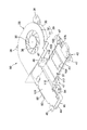
図2ないし図10に示すように、筐体4の内部には、半導体パッケージ19を冷却する冷却装置25が収容されている。冷却装置25は、回路基板17の右端部と筐体4の右側の側壁4dとの間に位置されている。この冷却装置25は、送風手段として機能する電動式のファンユニット26とヒートシンク27とを備えている。
【0044】
ファンユニット26は、偏平なファンケーシング29と、このファンケーシング29にモータ(図示せず)を介して支持された遠心ファン30とで構成されている。ファンケーシング29は、ベースパネル31と、このベースパネル31に連結されたアッパパネル32とを有している。
【0045】
ベースパネル31は、アルミニウム合金又はマグネシウム合金のような軽量で熱伝導性に優れた金属材料にて構成されている。ベースパネル31は、筐体4の底壁4aと向かい合っており、このベースパネル31の中央部からやや偏心した位置に円形の第1の吸込口33が開口されている。ベースパネル31は、第1の吸込口33の中央部に張り出すモータ支持部34を有し、このモータ支持部34の上面に偏平モータを介して上記遠心ファン30が支持されている。遠心ファン30は、その回転軸線O1を鉛直方向に沿わせた横置きの姿勢で配置されている。
【0046】
また、ベースパネル31は、その周縁部から上向きに延びる周壁35を有している。周壁35は、遠心ファン30を取り囲むように配置されており、この周壁35の二箇所に側方に張り出す支持片36が形成されている。
【0047】
なお、遠心ファン30は、上記ICチップ21の温度が予め決められた値に達した時に偏平モータによって回転駆動されるようになっている。
【0048】
アッパパネル32は、ステンレス鋼板のような金属材料にて構成されている。アッパパネル32は、周壁35の上端部に固定されており、上記ベースパネル31と平行に配置されている。アッパパネル32は、第2の吸込口38を有している。第2の吸込口38は、第1の吸込口33と向かい合っており、これら第1および第2の吸込口33,38の間に遠心ファン30が位置されている。また、アッパパネル32は、ベースパネル31との間に送風通路39(図9に示す)を構成しており、この送風通路39の上流端に第1および第2の吸込口33,38が開口されている。
【0049】
ファンケーシング29は、図6および図7から明らかなように、送風通路39の下流端に連なる吐出口40を有している。吐出口40は、ファンケーシング29の幅方向に延びるスリット状をなしており、上記支持片36とは反対側に位置されている。
【0050】
このような構成のファンユニット26において、遠心ファン30が回転駆動されると、第1および第2の吸込口33,38から遠心ファン30の軸方向に空気が吸い込まれる。この空気は、遠心ファン30の外周部からその径方向外側に向けて吐き出された後、送風通路39を通じて吐出口40に導かれ、ここからファンケーシング29の外方に吐出されるようになっている。
【0051】
図7に示すように、ファンケーシング29のベースパネル31は、ヒートシンク支持部42を一体に備えている。ヒートシンク支持部42は、ベースパネル31と重なり合うことなく平面的に並べて配置されており、これらヒートシンク支持部42とベースパネル31との境界部分に吐出口40が位置されている。
【0052】
ヒートシンク支持部42は、矩形状の枠部43と、この枠部43に連なる取り付けガイド44とを備えている。枠部43と取り付けガイド44とは、上記吐出口40の長手方向に沿って平面的に並べて配置されている。取り付けガイド44は、枠部43の各辺よりも幅広く形成された帯状をなしており、上記吐出口40から遠ざかる方向に水平に延びている。この取り付けガイド44は、複数の座部45を有している。座部45およびファンケーシング29の支持片36は、上記筐体4の底壁4aから上向きに突出する複数のボス部46に夫々ねじ止めされている。
【0053】
このため、ヒートシンク支持部42を含むファンケーシング29は、底壁4aに熱的に接続された状態で固定されており、これらヒートシンク支持部42とファンケーシング29とは筐体4の奥行き方向に並んでいる。
【0054】
ファンケーシング29を底壁4aに固定した状態では、図9に示すように、ヒートシンク支持部42の取り付けガイド44が筐体4の右側の側壁4dに沿って延びており、この側壁4dの排気口6に隣接されている。それとともに、図10に示すように、ベースパネル31の第1の吸込口33が底壁4aに開口された第2の吸入口5bに重なり合うとともに、アッパパネル32の第2の吸込口38が側壁4dに開口された第1の吸入口5aの近傍に位置されている。また、このアッパパネル32は、キーボード9の下面に対し僅かな隙間を存して向かい合っている。
【0055】
ヒートシンク支持部42の枠部43は、回路基板17の右端部の下方に入り込んでおり、この枠部43の各辺で囲まれた領域に対応する部分に半導体パッケージ19が位置されている。枠部43は、上向きに張り出す四つの受け座47を有している。受け座47は、半導体パッケージ19の四つの角部の外側において回路基板17の裏面17aに接しており、これら受け座47にねじ48を介して回路基板17が固定されている。
【0056】
この固定により、回路基板17上の半導体パッケージ19とヒートシンク支持部42との位置合わせがなされ、この半導体パッケージ19がファンケーシング29の吐出口40と部分的に向かい合っている。
【0057】
上記ヒートシンク27は、例えばアルミニウム合金又はマグネシウム合金のような軽量で熱伝導性に優れた金属材料にて構成されている。ヒートシンク27は、受熱部50および放熱部51を備えている。受熱部50は、平坦な長方形の板状をなしている。この受熱部50は、半導体パッケージ19を下方から覆うとともに、ヒートシンク支持部42の枠部43の内側に収まるような大きさを有している。このため、受熱部50は、枠部43の各辺によって取り囲まれている。
【0058】
受熱部50は、回路基板17の裏面17aと向かい合う上面52を有している。上面52の略中央部には、上向きに僅かに張り出す凸部53が形成されている。凸部53の上端は、平坦な受熱面54となっており、この受熱面54が半導体パッケージ19のICチップ21と向かい合うようになっている。
【0059】
放熱部51は、受熱部50と一体化されてこの受熱部50と熱的に接続されている。放熱部51は、受熱部50の一端において、この受熱部50と直交する方向に延びており、上記ヒートシンク支持部42の取り付けガイド44上に位置されている。
【0060】
放熱部51は、受熱部50に連なる底壁56を有している。底壁56は、受熱部50と同一平面上に位置されており、この底壁56の長手方向に沿う両側縁部に上向きに延びる一対の側壁57a,57bが形成されている。側壁57a,57bの上端には、金属製のカバープレート58が固定されている。
【0061】
カバープレート58は、回路基板17の右端部と筐体4の右側の側壁4dとの間において、回路基板17よりも上方に僅かに張り出しているとともに、上記キーボード9の下面に隣接されている。このカバープレート58は、底壁56および側壁57a,57bと協働して上記放熱部51に一つの冷却風通路59を構成している。
【0062】
図9に示すように、冷却風通路59は、上記ヒートシンク支持部42の取り付けガイド44に沿って筐体4の奥行き方向に直線状に延びている。この冷却風通路59は、冷却風入口61と冷却風出口62とを有している。冷却風入口61は、冷却風通路59の上流端に位置され、ファンケーシング29の吐出口40の一部と向かい合っている。冷却風出口62は、冷却風通路59の下流端に位置され、上記放熱部51の側方および後方に向けて連続して開口されている。
【0063】
冷却風出口62のうち、放熱部51の側面に位置する開口部分は、冷却風通路59の上流側における冷却風の流れ方向とは異なる方向に開口され、筐体4の排気口6と向かい合っている。また、冷却風出口62の後端は、筐体4の後壁4eの右端部と向かい合っており、これら後壁4eと底壁4aとで規定される角部には、複数の補助排気口60が開口されている。
【0064】
冷却風通路59に臨む底壁56の上面には、複数の板状をなす第1の冷却フィン63と、複数のピン状をなす第2の冷却フィン64とが配置されている。第1の冷却フィン63は、冷却風通路59の通路方向に沿って直線状に延びているとともに、互いに間隔を存して平行に配置されている。これら第1の冷却フィン63は、冷却風出口62よりも冷却風の流れ方向に沿う上流側に位置されている。
【0065】
第2の冷却フィン64は、冷却風出口62に臨む冷却風通路59の下流端に位置されている。これら第2の冷却フィン64は、格子状に並べて配置され、上記第1の冷却フィン63の下流端と向かい合っている。
【0066】
図3および図8に見られるように、ヒートシンク27は、平坦な下面を有している。このヒートシンク27の下面には、凹部66が形成されている。凹部66は、受熱部50と放熱部51とに跨って延びており、この凹部66内に熱移送手段として機能する偏平なヒートパイプ67が埋め込まれている。ヒートパイプ67は、第1の端部67aと第2の端部67bとを有している。第1の端部67aは、受熱部50に熱的に接続され、第2の端部67bは、放熱部51に熱的に接続されている。
【0067】
図2および図7に示すように、放熱部51の底壁56は、上向きに延びる一対の支点軸70a,70bを有している。一方の支点軸70aは冷却風入口61に位置され、他方の支点軸70bは冷却風出口62に位置されている。このため、支点軸70a,70bは、冷却風通路59の通路方向に互いに離間して配置されている。
【0068】
支点軸70a,70bは、ヒートシンク27の放熱部51をヒートシンク支持部42の取り付けガイド44上に載置した時に、この取り付けガイド44やファンケーシング29に形成した一対の支承壁71a,71bの下方に位置され、これら支点軸70a,70bの先端が支承壁71a,71bと向かい合っている。これら支点軸70a,70bは、受熱部50の受熱面54に対し放熱部51を挟んだ反対側に位置され、この受熱面54から遠ざかっている。
【0069】
ヒートシンク27の受熱部50は、貫通孔72を有している。貫通孔72は、放熱部51とは反対側に位置されており、これら貫通孔72と支点軸70a,70bとの間に受熱面54が位置されている。
【0070】
図4に示すように、受熱部50を囲む枠部43は、その一辺に貫通孔72の下方に張り出す壁部73を有している。壁部73の上面には、上向きに突出する円柱状のねじ受け部74が形成されている。ねじ受け部74の高さ寸法は、受熱部50の厚み寸法よりも大きく設定されており、このねじ受け部74が上記貫通孔72に遊びを以って挿入されている。ねじ受け部74の上端には、ワッシャ75を介してねじ76がねじ込まれている。ワッシャ75は、貫通孔72よりも大径に形成されており、ねじ受け部74の上面および受熱部50の上面52に重ね合わされるようになっている。
【0071】
このため、ヒートシンク27は、支点軸70a,70bおよび貫通孔72の位置でヒートシンク支持部42に引っ掛かっており、上記ワッシャ75と受熱部50の上面52との間の隙間寸法S(図4に示す)に対応する分だけ、筐体4の厚み方向に上下動が可能となっている。
【0072】
図7および図8に示すように、枠部43には、弾性体として機能する板ばね80が支持されている。板ばね80は、枠部43の互いに向かい合う二辺の間に跨っており、受熱部50の下方において筐体4の奥行き方向に延びている。板ばね80は、冷却装置25を平面的に見た場合に、受熱部50の受熱面54と放熱部51との間に位置されている。
【0073】
この板ばね80の中間部には、上向きに円弧状に湾曲された押圧部81が形成されている。押圧部81は、受熱部50と放熱部51とを含めたヒートシンク27の重心位置Gもしくはその近傍において、受熱部50の下面に弾性的に接しており、この受熱部50を押し上げている。
【0074】
このことにより、ヒートシンク27の支点軸70a,70bの先端が支承壁71a,71bに突き当たるとともに、受熱部50の上面52がワッシャ75に突き当たっている。そのため、ヒートシンク27は、支点軸70a,70bと支承壁71a,71bとの接触部を支点として、受熱部50の受熱面54が半導体パッケージ19に近づいたり遠ざかる方向に回動し得るようにヒートシンク支持部42に浮動的に支持されているとともに、常に受熱面54が半導体パッケージ19に近づく方向に弾性的に付勢されている。
【0075】
また、図9に最も良く示されるように、冷却装置25を平面的に見た場合、ヒートシンク27の回動支点となる支点軸70a,70bと、ワッシャ75と受熱部50との接触部とは、丁度三角形の頂点の位置関係に設定され、ヒートシンク支持部42に対するヒートシンク27の取り付け姿勢の安定性が高められている。
【0076】
受熱部50の受熱面54と半導体パッケージ19のICチップ21との間には、伝熱シート82が介在されている。伝熱シート82は、例えばシリコーン樹脂にアルミナを添加してなるゴム状の弾性体であり、熱伝導性を有している。伝熱シート82は、上記板ばね80によるヒートシンク27の押圧に伴い、受熱面54とICチップ21との間で弾性的に挟み込まれており、この伝熱シート82を介して受熱面54とICチップ21とが熱的に接続されている。
【0077】
このような構成のポータブルコンピュータ1において、半導体パッケージ19のICチップ21が発熱すると、このICチップ21の熱は伝熱シート82を介してヒートシンク27の受熱部50に伝えられる。
【0078】
また、ヒートシンク27の受熱部50と放熱部51とはヒートパイプ67を介して熱的に接続されているので、ICチップ21から受熱部50に伝えられた熱の一部は、ヒートパイプ67の第1の端部67aに伝えられる。これにより、ヒートパイプ67に封入されている作動液が加熱されて蒸気となり、この蒸気は第1の端部67aから第2の端部67bに向けて流動する。
【0079】
ヒートパイプ67の第2の端部67bに導かれた蒸気は、ここで放熱し凝縮する。この凝縮により液化された作動液は、毛細管力により第2の端部67bから第1の端部67aに向けて還流し、再度ICチップ21の熱を受けて加熱される。この作動液の蒸発および凝縮の繰り返しにより、受熱部50の熱が放熱部51に積極的に移される。
【0080】
したがって、受熱部50に伝えられたICチップ21の熱は、ヒートシンク27全体に拡散されるとともに、この拡散による自然空冷により放出される。
【0081】
ICチップ21の温度が予め規定された値に達すると、ファンユニット26の遠心ファン30が回転駆動される。この遠心ファン30の回転により、筐体4の外部の空気が第1および第2の吸入口5a,5bを通じて筐体4の内部に吸い込まれる。この空気は、第1および第2の吸込口33,38から遠心ファン30の軸方向に吸い込まれた後、遠心ファン30の外周部から送風通路39に吐き出され、冷却風となってファンケーシング29の吐出口40から吐出される。
【0082】
この吐出口40の一部は、冷却風通路59の冷却風入口61に連なるとともに、吐出口40の残りの部分は、筐体4の内部に開放されて半導体パッケージ19と向かい合っている。このため、冷却風は冷却風通路59および半導体パッケージ19の双方に夫々導かれる。
【0083】
冷却風通路59内には、通路方向に延びる複数の第1の冷却フィン63が存在するので、冷却風は第1の冷却フィン63に沿って流れた後、冷却風通路59の下流端に達する。冷却風通路59の下流端には、ピン状の複数の第2の冷却フィン64が格子状に並べて配置されているので、第1の冷却フィン63を通過して冷却風通路59の下流端に到達した冷却風は、第2の冷却フィン64の間を縫うようにして通り抜ける。
【0084】
このため、放熱部51と冷却風との接触面積が増大し、この冷却風によってヒートシンク27の放熱部51が強制的に冷却される。よって、放熱部51の放熱性能が向上し、この放熱部51に伝えられたICチップ21の熱を冷却風の流れに乗じて効率良く放出することができる。
【0085】
また、図9に矢印で示すように、冷却風通路59の下流端では、冷却風がピン状の第2の冷却フィン64を避けるようにして流れることから、この冷却風の流れが乱流となり、これら第2の冷却フィン64によって冷却風の流れを排気口6に向けて曲げることができる。このため、放熱部51を強制的に冷却した冷却風の多くは、筐体4の側壁4dの排気口6から外部に排出されるとともに、残りは冷却風通路59の冷却風出口62から後方に流れ、筐体4の後端の補助排気口60を通じて外部に排出される。
【0086】
冷却風通路59の下流端において冷却風の流れが乱流となれば、この冷却風は全ての第2の冷却フィン64に接するように拡散され、第2の冷却フィン64に冷却風が万遍なく接触する。このため、冷却風通路59の下流端において、放熱部51と冷却風との接触面積を充分に確保することができ、この放熱部51の放熱性能を高めることができる。
【0087】
加えて、何らかの理由により筐体4の排気口6が部分的に閉塞されたとしても、冷却風は閉塞部分を避けるように、隣り合う第2の冷却フィン64の間を通じて冷却風通路59の下流端の他の場所に流れ込む。このため、冷却風の流れが阻害されずに済むので、冷却風通路59内を流れる冷却風の風量を確保することができ、放熱部51の放熱性能を良好に維持することができる。
【0088】
また、ファンケーシング29から吐出される冷却風は、冷却風通路59ばかりでなく、半導体パッケージ19にも直接導かれるので、この半導体パッケージ19の周囲に冷却風の流れが生じ、この冷却風の流れに基づく強制対流により半導体パッケージ19や受熱部50が冷やされる。それとともに、筐体4の内部を冷却風が流通するので、筐体4の内部の通気性が良好となり、半導体パッケージ19の周囲に熱溜りが生じ難くなる。
【0089】
この結果、半導体パッケージ19の放熱性能をより高めることができる。
【0090】
なお、図9から明らかなように、冷却風出口62の一部は放熱部51の側壁57aに開口されているので、この側壁57aに沿って冷却風通路59を流れる冷却風は、冷却風入口61から冷却風出口62までの距離が短くなり、これよりも冷却風通路59の中央部分を流れる冷却風は、冷却風入口61から冷却風出口62までの距離が長くなる。
【0091】
すなわち、冷却風通路59の中央部では、側壁57aに沿う部分に比べて冷却風の流通抵抗が大きくなり、それ故、冷却風通路59の中央部を流れる冷却風の風量が少なくなって、冷却風通路59の中央部に位置する第2の冷却フィン64を放熱用として有効に活用することができなくなることがあり得る。
【0092】
このような場合には、側壁57aに近い第2の冷却フィン64間のピッチを狭くして、この側壁57aに沿って流れる冷却風の通風抵抗を故意に増やすようにすれば、冷却風通路59内での冷却風の風量の分布を均等化することができる。したがって、全ての第2の冷却フィン64に万遍なく冷却風を導くことができ、放熱部51の放熱性能を高めることができる。
【0093】
ところで、上記構成の冷却装置25によると、半導体パッケージ19の熱を受けるヒートシンク27は、ファンケーシング29のヒートシンク支持部42に浮動的に支持され、回路基板17上の半導体パッケージ19に対し近づいたり遠ざかる方向に回動可能であるとともに、常に板ばね80を介して半導体パッケージ19のICチップ21に近づく方向に弾性的に付勢されている。
【0094】
このため、回路基板17に対する半導体パッケージ19の実装高さ、あるいはヒートシンク27の受熱部50の厚み寸法にばらつきが生じたとしても、ヒートシンク27がその支点軸70a,70bと支承壁71a,71bとの接触部を支点に上下方向に回動することで上記実装高さや厚み寸法のばらつき分を吸収する。
【0095】
しかも、ヒートシンク27の受熱部50は、板ばね80を介してICチップ21に押し付けようとする力を受けているので、受熱部50の受熱面54とICチップ21との密着性を高めることができる。このため、受熱面54とICチップ21との間に伝熱シート82を介在させるにしても、この伝熱シート82に実装高さや厚み寸法のばらつき分を吸収する機能を付加する必要はない。
【0096】
よって、伝熱シート82は、受熱面54とICチップ21との局部的な接触を阻止して、ICチップ21の熱を受熱面54の全面に亙って分散し得る程度の肉厚を有していれば良いことになり、この伝熱シート82を必要最小限度まで薄くすることができる。この結果、ヒートシンク27とICチップ21との熱接続部分に生じる熱抵抗を低減することができ、ICチップ21の熱を効率良くヒートシンク27に通じて外方に放出することができる。
【0097】
また、上記構成によると、ヒートシンク27の回動支点となる支点軸70a,70bは、受熱部50の受熱面54に対し放熱部51を挟んだ反対側に位置されているので、この支点軸70a,70bから受熱面54までの距離が長くなる。このため、ヒートシンク27を上下方向に回動させるようにしたにも拘わらず、このヒートシンク27の受熱面54は、ICチップ21に対して略平行な状態を保ったまま上下動することになる。この結果、ICチップ21に対する受熱面54の局部的な接触を回避することができ、これらICチップ21と受熱面54との接触状態を良好に維持することができる。
【0098】
さらに、ヒートシンク27の受熱部50と放熱部51とは、互いに重なり合うことなく平面的に並べて配置されているので、ICチップ21から受熱部50を通じて放熱部51に至るまでの熱伝達経路を偏平なものとすることができる。このため、ヒートシンク27を薄くコンパクトに形成することができ、薄型化が強化された筐体4の内部に無理なく組み込むことができる。
【0099】
加えて、冷却風通路59を有する放熱部51は、回路基板17から外れているので、冷却風通路59の天井となるアッパパネル32の位置が回路基板17によって制限されることはなく、このアッパパネル32を回路基板17の上面と略同一高さに位置させることができる。このため、冷却風通路59の高さ寸法を増して通路断面積を充分に確保することができ、ここを流れる冷却風の流量を増やすことができる。
【0100】
それとともに、第1および第2の冷却フィン63,64の高さも確保し易くなり、これら冷却フィン63,64と冷却風との接触面積を増やすことができる。この結果、上記冷却風の風量増加と合わせて、放熱部51の放熱性能をより一層高めることができる。
【0101】
また、板ばね80の押圧部81は、ヒートシンク27の重心位置G又はその近傍において受熱部50の下面に接しているので、例えばポータブルコンピュータ1に振動が加わった場合でも、浮動状態にあるヒートシンク27が独立して振動し難くなる。このため、ICチップ21が受熱面54によって叩かれたり、過大な押圧力を受けることはなく、半導体パッケージ19の耐衝撃性を高めることができる。
【0102】
さらに、上記構成の冷却装置25によれば、ファンユニット26のファンケーシング29にヒートシンク支持部42を形成したことにより、このヒートシンク支持部42を単にヒートシンク27を取り囲むような枠状に形成することができ、ヒートシンク支持部42の質量を小さくできる。
【0103】
このため、ヒートシンク27を含めた冷却装置25全体の軽量化が可能となり、例えばポータブルコンピュータ1に振動が加わった場合でも、筐体4と冷却装置25との連結部分に作用する荷重を低減することができ、この冷却装置25の取り付け構造を簡略化することができる。
【0104】
なお、上記第1の実施の形態では、ヒートシンクの放熱部に一つの冷却風通路を形成したが、本発明はこれに限らず、放熱部に複数の冷却風通路を形成しても良い。
【0105】
さらに、上記第1の実施の形態によると、受熱部を押圧する板ばねは、受熱部の重心位置又はその近傍において受熱部の下面に接しているが、本発明はこれに限らず、例えば受熱部の重心位置を間に挟んだ二箇所において受熱部の下面に接触させるようにしても良い。
【0106】
加えて、ヒートシンク支持部の枠部は、ヒートシンクの受熱部を周方向に連続して取り囲む必要はなく、この枠部の一部が途切れていても良い。
【0107】
また、本発明は上記第1の実施の形態に特定されるものではなく、図11ないし図14に本発明の第2の実施の形態を示す。
【0108】
この第2の実施の形態に係る冷却装置90は、主にICチップ21の熱を受けるヒートシンク91の構成と、このヒートシンク91を浮動的に支持するための構成が上記第1の実施の形態と相違しており、それ以外の冷却装置90の基本的な構成は上記第1の実施の形態と同様である。このため、第2の実施の形態において、第1の実施の形態と同一の構成部分には同一の参照符号を付して、その説明を省略する。
【0109】
図12に示すように、ヒートシンク支持部42の取り付けガイド44は、枠部43とは反対側の縁部に上向きに延びる第1の側壁92を有している。この側壁92のファンケーシング29とは反対側の先端部には、第1の冷却風出口93が形成されている。第1の冷却風出口93は、筐体4の側壁4dの排気口6と向かい合うようになっている。
【0110】
また、取り付けガイド44は、第1の冷却風出口93と向かい合う位置に上向きに延びる第2の側壁94を有している。第2の側壁94は、第1の側壁92との間に第2の冷却風出口95を構成しており、この第2の冷却風出口95は筐体4の後壁4eに向けて開口されている。
【0111】
ヒートシンク支持部42の枠部43は、第1の嵌合部として機能する一対の嵌合凸部97a,97bを有している。嵌合凸部97a,97bは、枠部43の互いに向かい合う二辺に形成されている。これら嵌合凸部97a,97bは、夫々枠部43の上面から上向きに突出されているとともに、筐体4の奥行き方向に沿って互いに平行に配置されている。
【0112】
図12や図14の(A)に示すように、ヒートシンク91は、受熱部100と放熱部101とを有している。受熱部100は、半導体パッケージ19を下方から覆うとともに、上記枠部43の内側に収まる大きさを有する長方形状をなしている。この受熱部100は、回路基板17の裏面17aと向かい合う上面102を有している。上面102の略中央部には、上向きに僅かに張り出す凸部103が形成されている。凸部103の上端は、平坦な受熱面104となっており、この受熱面104が半導体パッケージ19のICチップ21と向かい合うようになっている。
【0113】
また、受熱部100は、平坦な下面106を有している。この下面106には、第2の嵌合部として機能する一対の嵌合凹部107a,107bが形成されている。嵌合凹部107a,107bは、筐体4の奥行き方向に延びるスリット状をなしており、これら嵌合凹部107a,107bの間に上記受熱面104が位置されている。
【0114】
受熱部100の嵌合凹部107a,107bと枠部43の嵌合凸部97a,97bとは、上下方向に移動可能に互いに嵌合されている。この嵌合により、ヒートシンク91がヒートシンク支持部42に上下方向に移動可能に支持され、ヒートシンク91が半導体パッケージ19に近づいたり遠ざかる方向に上下動されるようになっている。
【0115】
そして、図14の(B)に示すように、嵌合凸部97a,97bと嵌合凹部107a,107bとの間には、これら両者の相対的な移動を許容するための隙間108が形成されており、この隙間108に熱伝導部材としての柔軟なグリス109が充填されている。グリス109は、空気よりも大きな熱伝導率を有し、このグリス109を介してヒートシンク91とヒートシンク支持部42とが熱的に接続されている。
【0116】
ヒートシンク91の放熱部101は、取り付けガイド44と向かい合う長方形状をなしている。放熱部101は、連結壁110を介して受熱部100の一端に連なっており、この受熱部100と一体化されている。連結壁110は受熱部100の一端から上向きに延びている。そのため、放熱部101は、受熱部100よりも上方に位置され、回路基板17と同一面上に位置されている。
【0117】
放熱部101は、取り付けガイド44、第1および第2の側壁92,94および連結壁110と協働して冷却風通路111を構成している。この冷却風通路111の上流端は、ファンケーシング29の吐出口40に連なり、冷却風通路111の下流端は、上記第1および第2の冷却風出口93,95に連なっている。
【0118】
冷却風通路111に臨む放熱部101の下面には、多数のピン状をなす放熱フィン112が突設されている。放熱フィン112は、冷却風通路111の内部において格子状に並べて配置されている。
【0119】
図12ないし図14に示すように、ヒートシンク支持部42の枠部43には、弾性体として機能するばね部材115が取り付けられている。ばね部材115は、半球状の押圧部116と、この押圧部116から放射状に延びる四本のアーム部117とを有している。
【0120】
アーム部117の先端は、座部45の下端にねじ118を介して固定されており、この固定により、押圧部116が枠部43の各辺で囲まれた空間の略中央部に位置されている。そして、ばね部材115の押圧部116は、嵌合凹部107a,107bの間において、ヒートシンク91の受熱部100の下面106に弾性的に接触し、この受熱部100を押し上げている。そのため、ヒートシンク91は、常に受熱面104が半導体パッケージ19に近づく方向に弾性的に付勢されている。
【0121】
このような構成によると、半導体パッケージ19の熱を受けるヒートシンク91は、ヒートシンク支持部42に対し上下動可能に浮動的に支持されているとともに、ばね部材115を介して常に半導体パッケージ19のICチップ21に近づく方向に弾性的に付勢されている。
【0122】
このため、回路基板17に対する半導体パッケージ19の実装高さ、あるいはヒートシンク91の受熱部100の厚み寸法にばらつきが生じたとしても、ヒートシンク91が嵌合凸部97a,97bと嵌合凹部107a,107bとの嵌合部分をガイドとして上下方向に昇降動することで上記実装高さや厚み寸法のばらつき分を吸収する。
【0123】
しかも、ヒートシンク91の受熱部100は、ばね部材115を介してICチップ21に押し付けようとする力を受けているので、受熱部100の受熱面104とICチップ21との密着性を高めることができる。このため、受熱面104とICチップ21との間に伝熱シート82を介在させるにしても、この伝熱シート82に実装高さや厚み寸法のばらつきを吸収する機能を付加する必要はない。
【0124】
よって、伝熱シート82は、受熱面104とICチップ21との局部的な接触を阻止して、ICチップ21の熱を受熱面104の全面に亙って分散し得る程度の肉厚を有していれば良く、この伝熱シート82を必要最小限度まで薄くすることができる。この結果、上記第1の実施の形態と同様に、ヒートシンク91とICチップ21との熱接続部分に生じる熱抵抗を低減することができ、ICチップ21の熱を効率良くヒートシンク91を通じて外方に放出することができる。
【0125】
また、受熱部100と放熱部101とは、互いに重なり合うことなく平面的に並べて配置されているので、ICチップ21から受熱部100を通じて放熱部101に至るまでの熱伝達経路を偏平なものとすることができ、筐体4の薄型化にも無理なく対応することができる。
【0126】
しかも、上記構成によると、ヒートシンク91の受熱部100とヒートシンク支持部42の枠部43とは、嵌合凸部97a,97bと嵌合凹部107a,107bとの嵌合部分を通じて熱的に接続されているので、受熱部100に伝えられたICチップ21の熱を枠部43からファンケーシング29に積極的に逃すことができる。このため、ヒートシンク支持部42およびこれに連なるファンケーシング29を放熱部品として積極的に活用することができ、ヒートシンク91の放熱性能をより高めることができる。
【0127】
加えて、嵌合凸部97a,97bと嵌合凹部107a,107bとの嵌合部分に生じる隙間108にグリス109が充填されているので、受熱部100と枠部43との熱接続部分の熱抵抗を小さく抑えることができる。
【0128】
それとともに、冷却装置90に外部から振動が作用した時に、ばね部材115を介して浮動的に支持されたヒートシンク91の振動をグリス109によって減衰することができる。このため、ICチップ21が受熱面104によって叩かれたり、過大な押圧力を受けることはなく、半導体パッケージ19の耐衝撃性を高めることができるといった利点がある。
【0129】
なお、本発明は上記実施の形態に特定されるものではなく、発明の主旨を逸脱しない範囲内で種々変形して実施可能である。
【0130】
例えば上記各実施の形態では、半導体パッケージのICチップとヒートシンクの受熱部との間に伝熱シートを介在させるようにしたが、この伝熱シートの代わりに熱伝導性のグリスを介在させても良いとともに、場合によっては伝熱シートやグリスを省略し、受熱部をICチップに直接接触させるようにしても良い。
【0131】
また、ヒートシンクの受熱部と放熱部とは必ずしも一体成形する必要はなく、例えば互いに区画された受熱部と放熱部とをねじ等で結合しても良い。
【0132】
【発明の効果】
以上詳述した本発明によれば、発熱部品の実装高さ、あるいはヒートシンクの受熱部の厚み寸法にばらつきが生じたとしても、このヒートシンクが移動することで上記実装高さや厚み寸法のばらつき分を吸収する。しかも、受熱部は常に弾性体を介して発熱部品に押し付けようとする力を受けているので、これら受熱部と発熱部品との密着性が良好となる。
【0133】
このため、受熱部と発熱部品との間に熱伝導性シート又はグリスのような熱伝導部材を介在させるにしても、この熱伝導部材に実装高さや厚み寸法のばらつきを吸収する機能を付加する必要はなく、この熱伝導部材を必要最小限度まで薄くすることができる。したがって、ヒートシンクと発熱部品との熱接続部分に生じる熱抵抗を低減することができ、この発熱部品の熱を効率良くヒートシンクを通じて外部に放出することができる。
【0134】
しかも、受熱部と放熱部とは互いに重なり合うことなく配置されるので、発熱部品から受熱部を通じて放熱部に至るまでの熱伝達経路を偏平なものとすることができ、筐体の薄型化に無理なく対応することができる。
【図面の簡単な説明】
【図1】本発明の第1の実施の形態に係るポータブルコンピュータの斜視図。
【図2】筐体の内部に冷却装置を組み込んだ状態を示すポータブルコンピュータの断面図。
【図3】(A)は、筐体の内部に冷却装置を組み込んだ状態を示すポータブルコンピュータの断面図。(B)は、送風通路と受熱部との位置関係を示すポータブルコンピュータの断面図。
【図4】 BGA形の半導体パッケージとヒートシンクの受熱部との接続部分を示す断面図。
【図5】回路基板に冷却装置を固定した状態を示す斜視図。
【図6】冷却装置の斜視図。
【図7】ファンユニットとヒートシンクとを分離させた状態を示す冷却装置の斜視図。
【図8】筐体の底壁、冷却装置およびBGA形の半導体パッケージとの位置関係を示す斜視図。
【図9】筐体の内部に冷却装置を収容した状態を示すポータブルコンピュータの断面図。
【図10】筐体の内部に冷却装置を収容した状態を示すポータブルコンピュータの底面図。
【図11】本発明の第2の実施の形態に係る冷却装置の斜視図。
【図12】ファンユニットとヒートシンクとを分離させた状態を示す冷却装置の斜視図。
【図13】冷却装置の底面図。
【図14】(A)は、筐体の内部に冷却装置を組み込んだ状態を示すポータブルコンピュータの断面図。
(B)は、図14の(A)のA部を拡大して示す断面図。
【符号の説明】
4…筐体、4a…底壁、17…回路基板、19…発熱部品(半導体パッケージ)、27,91…ヒートシンク、29…ファンケーシング、30…ファン(遠心ファン)、50,100…受熱部、51,101…放熱部、54…受熱面、67…ヒートパイプ、80,115…弾性体(板ばね、ばね部材)[0001]
BACKGROUND OF THE INVENTION
The present invention relates to a cooling device for promoting heat dissipation from a heat-generating component such as a semiconductor package, and an electronic device such as a portable computer equipped with the cooling device.
[0002]
[Prior art]
Portable electronic devices typified by book-type portable computers and mobile information devices, such as MPUs (Micro Processing Units) and gate arrays for processing versatile multimedia information such as text, audio, and images Equipped with a semiconductor package. In this type of semiconductor package, the power consumption continues to increase as the processing speed increases and the number of functions increases, and the amount of heat generated during operation tends to increase rapidly in proportion thereto.
[0003]
Therefore, in order to guarantee the stable operation of the semiconductor package, it is necessary to improve the heat dissipation of the semiconductor package. Therefore, various heat dissipation / cooling means such as a heat sink and a heat pipe are indispensable. .
[0004]
A conventional heat sink includes a heat receiving portion that receives heat from the semiconductor package and a heat radiating portion that is thermally connected to the heat receiving portion. The heat sink is rigidly fixed to a circuit board on which the semiconductor package is mounted, and the semiconductor package is thermally connected to the heat receiving portion of the heat sink.
[0005]
At this time, if a gap exists between the heat receiving portion of the heat sink and the semiconductor package, this gap functions as a kind of heat insulating layer, and heat transfer from the semiconductor package to the heat receiving portion is hindered. For this reason, conventionally, a thermally conductive grease is filled between the heat receiving portion of the heat sink and the semiconductor package, or a rubber heat transfer sheet having a thermal conductivity is interposed between the heat receiving portion and the semiconductor package. Increases adhesion.
[0006]
By the way, as an MPU for a portable computer, a BGA type semiconductor package is generally used. When this type of semiconductor package is mounted on a circuit board, the mounting height with respect to the circuit board may vary within a range of ± 0.25 mm.
[0007]
In addition, since an aluminum alloy injection molded product with excellent thermal conductivity is used for the heat sink, dimensional tolerances may occur in each part including the heat receiving part. The height dimension from the heat receiving portion to the circuit board may vary.
[0008]
For this reason, conventionally, when the semiconductor package and the heat receiving portion of the heat sink are thermally connected using the heat transfer sheet, the thickness of the heat transfer sheet exceeds the maximum value of the gap caused by the dimensional tolerance or the like. By setting the value to a value and elastically deforming the thick heat transfer sheet between the semiconductor package and the heat receiving portion, variations in the mounting height of the semiconductor package and the dimensional tolerance of the heat sink are absorbed.
[0009]
[Problems to be solved by the invention]
However, a flexible rubber-like elastic body such as a heat transfer sheet is generally low in density and has a low heat conduction performance compared to a metal material. Therefore, a conventional structure that necessitates the use of a thick heat transfer sheet. Then, a large thermal resistance is generated at the thermal connection portion between the semiconductor package and the heat receiving portion.
[0010]
For this reason, it becomes impossible to efficiently transfer the heat of the semiconductor package to the heat sink, and there is room for improvement in improving the heat dissipation of the semiconductor package.
[0011]
Conventionally, a heat sink and an electric fan are used in combination for cooling a semiconductor package having a large heat generation amount. The electric fan includes a fan that is rotationally driven and a fan casing that supports the fan, and is housed in a portable computer casing together with the heat sink. And the conventional heat sink has a fan attachment part which supports an electric fan, and a fan casing is piled up and fixed to this fan attachment part.
[0012]
However, recent portable computers have a thin and compact casing for the purpose of improving operability and portability. Therefore, the electric fan has the rotation axis of the fan along the thickness direction of the casing. It is housed inside the housing in a horizontal orientation. For this reason, when compared with the case where the electric fan is erected, the planar shape of the fan casing is increased, and the fan mounting portion for supporting the fan casing must be enlarged.
[0013]
Therefore, in the conventional configuration in which the fan mounting portion is formed on the heat sink, the heat sink itself is heavy and large, which hinders weight reduction of the portable computer. At the same time, when vibration is applied to the heat sink, the load burden on the heat sink attachment portion increases, and this load may function as a stress on the heat sink attachment portion. Therefore, the heat sink mounting portion must be firmly formed so as to be able to withstand stress, and the structure becomes complicated.
[0014]
Further, a conventional heat sink is known in which a duct is formed in the heat radiating portion and cooling air blown from an electric fan is guided to the duct. The duct has a cooling air outlet for discharging cooling air at the downstream end thereof, and this cooling air outlet is connected to an exhaust port formed in the housing.
[0015]
According to this type of heat sink, the heat radiating portion is forcibly cooled by the cooling air flowing through the duct, and the heat of the semiconductor package transmitted to the heat radiating portion is discharged to the outside of the housing by the flow of the cooling air. It is like that.
[0016]
By the way, when the cooling air outlet of the duct is opened in a direction different from the blowing direction of the cooling air, conventionally, a plurality of guide walls curved or bent toward the cooling air outlet are formed at the downstream end of the duct. These guide walls guide the cooling air toward the cooling air outlet. Adjacent guide walls constitute a plurality of groove-shaped discharge passages at the downstream end of the duct, and the downstream ends of these discharge passages are connected to the exhaust port of the housing.
[0017]
However, since the plurality of discharge passages are separated from each other by the guide wall, if the downstream end of a specific discharge passage is blocked for some reason, there is no escape space for cooling air flowing through the discharge passage, and cooling Wind resistance increases. For this reason, the air volume of the cooling air flowing through the duct is reduced, and there arises a problem that the heat radiation effect of the heat radiating portion by the cooling air is lowered.
[0018]
Of the present inventionThe purpose is an electronic device that can efficiently dissipate the heat of the heat-generating component to the heat sink, and that can enhance the thinning.There is in getting.
[0021]
[Means for Solving the Problems]
the abovethe purposeIn order to achieve the above, according to one embodiment of the present inventionElectronicsIs
A housing having a bottom wall;
A circuit board housed in the housing and facing the bottom wall;
A heat generating component mounted on the circuit board;
A heat receiving surface facing the heat generating component, a heat receiving portion movable toward and away from the heat generating component, and a surface protruding from the circuit board toward the bottom wall at a position away from the circuit board. A heat sink including a heat dissipating part, and a heat pipe straddling between the heat receiving part and the heat dissipating part along the circuit board,
A fan housed in the housing and sending wind to the heat radiating portion;
An elastic body that presses the heat receiving portion from the side opposite to the heat receiving surface toward the heat generating component;It is characterized by having.
[0023]
According to such a configuration, since the heat receiving portion of the heat sink is installed in a floating manner with respect to the heat generating component, even if the height dimension of the heat generating component varies or a dimensional tolerance occurs in the heat receiving portion. The dimensional error and dimensional tolerance are absorbed by the movement of the heat receiving portion.
[0024]
In addition, since the heat receiving portion of the heat sink receives a force that is always pressed against the heat generating component via the elastic body, the adhesion between the heat receiving portion and the heat generating component is improved. For this reason, even if a flexible heat conducting member such as a heat transfer sheet is interposed between the heat receiving part and the heat generating part, the heat conducting member absorbs dimensional errors and tolerances of the heat generating part and the heat receiving part. It is not necessary to add the heat conduction member, and the heat conduction member can be made as thin as necessary.
[0025]
Therefore, it is possible to reduce the thermal resistance of the heat connection portion between the heat generating component and the heat receiving portion, and to efficiently transfer the heat of the heat generating component to the heat sink.
[0026]
Further, according to the above configuration, the heat receiving portion and the heat radiating portion, and the heat radiating portion and the heat generating component do not overlap each other, so that the heat transfer path from the heat generating component to the heat radiating portion through the heat receiving portion can be made flat. Therefore, the heat sink can be formed to be thin and compact, and the housing can be easily reduced in thickness.
[0033]
DETAILED DESCRIPTION OF THE INVENTION
A first embodiment of the present invention will be described below with reference to FIGS. 1 to 10 applied to a portable computer.
[0034]
FIG. 1 discloses a book-type portable computer 1 as an electronic device. The portable computer 1 includes a computer
[0035]
The computer
[0036]
Further, a large number of
[0037]
The
[0038]
The
[0039]
The
[0040]
As shown in FIG. 3, a
[0041]
As shown in FIGS. 4 and 8, the
[0042]
Since the
[0043]
As shown in FIGS. 2 to 10, a
[0044]
The
[0045]
The
[0046]
The
[0047]
The
[0048]
The
[0049]
As is clear from FIGS. 6 and 7, the
[0050]
In the
[0051]
As shown in FIG. 7, the
[0052]
The heat
[0053]
For this reason, the
[0054]
Fan casing299 is fixed to the
[0055]
The
[0056]
With this fixing, the
[0057]
The
[0058]
The
[0059]
The
[0060]
The
[0061]
The
[0062]
As shown in FIG. 9, the cooling
[0063]
Of the cooling
[0064]
A plurality of plate-like
[0065]
The
[0066]
As seen in FIGS. 3 and 8, the
[0067]
As shown in FIGS. 2 and 7, the
[0068]
The
[0069]
The
[0070]
As shown in FIG. 4, the
[0071]
For this reason, the
[0072]
As shown in FIGS. 7 and 8, the
[0073]
A
[0074]
As a result, the tips of the
[0075]
Further, as best shown in FIG. 9, when the
[0076]
A
[0077]
In the portable computer 1 having such a configuration, when the
[0078]
Further, since the
[0079]
The steam guided to the
[0080]
Therefore, the heat of the
[0081]
When the temperature of the
[0082]
A part of the
[0083]
Since there are a plurality of
[0084]
For this reason, the contact area between the
[0085]
Further, as shown by the arrows in FIG. 9, the cooling air flows so as to avoid the pin-like
[0086]
If the flow of the cooling air becomes a turbulent flow at the downstream end of the cooling
[0087]
In addition, even if the
[0088]
Further, since the cooling air discharged from the
[0089]
As a result, the heat dissipation performance of the
[0090]
As is clear from FIG. 9, since a part of the cooling
[0091]
That is, in the central portion of the cooling
[0092]
In such a case, if the pitch between the
[0093]
By the way, according to the
[0094]
For this reason, even if the mounting height of the
[0095]
In addition, since the
[0096]
Therefore, the
[0097]
Further, according to the above configuration, the
[0098]
Furthermore, since the
[0099]
In addition, since the
[0100]
At the same time, the height of the first and
[0101]
Further, since the
[0102]
Furthermore, according to the
[0103]
For this reason, it is possible to reduce the weight of the
[0104]
In the first embodiment, one cooling air passage is formed in the heat radiating portion of the heat sink. However, the present invention is not limited to this, and a plurality of cooling air passages may be formed in the heat radiating portion.
[0105]
Furthermore, according to the first embodiment, the leaf spring that presses the heat receiving portion is in contact with the lower surface of the heat receiving portion at or near the center of gravity of the heat receiving portion. You may make it contact the lower surface of a heat receiving part in two places on both sides of the gravity center position of a part.
[0106]
In addition, the frame portion of the heat sink support portion does not need to continuously surround the heat receiving portion of the heat sink in the circumferential direction, and a part of the frame portion may be interrupted.
[0107]
The present invention is not limited to the first embodiment described above, and FIGS. 11 to 14 show a second embodiment of the present invention.
[0108]
The
[0109]
As shown in FIG. 12, the
[0110]
The mounting
[0111]
The
[0112]
As shown in FIG. 12 and FIG. 14A, the
[0113]
In addition, the
[0114]
The fitting
[0115]
As shown in FIG. 14B, a
[0116]
The
[0117]
The
[0118]
A large number of pin-shaped radiating
[0119]
As shown in FIGS. 12 to 14, a
[0120]
The distal end of the
[0121]
According to such a configuration, the
[0122]
For this reason, even if the mounting height of the
[0123]
In addition, since the
[0124]
Therefore, the
[0125]
Moreover, since the
[0126]
Moreover, according to the above configuration, the
[0127]
In addition, since
[0128]
At the same time, when the vibration is applied to the
[0129]
Note that the present invention is not limited to the above-described embodiment, and can be variously modified and implemented without departing from the spirit of the invention.
[0130]
For example, in each of the above embodiments, the heat transfer sheet is interposed between the IC chip of the semiconductor package and the heat receiving portion of the heat sink. However, instead of this heat transfer sheet, heat conductive grease may be interposed. In addition, in some cases, the heat transfer sheet or grease may be omitted, and the heat receiving portion may be directly in contact with the IC chip.
[0131]
In addition, the heat receiving portion and the heat radiating portion of the heat sink do not necessarily have to be integrally formed.
[0132]
【The invention's effect】
According to the present invention described in detail above, even if a variation occurs in the mounting height of the heat generating component or the thickness dimension of the heat receiving portion of the heat sink, the variation in the mounting height and thickness dimension can be reduced by moving the heat sink. Absorb. In addition, since the heat receiving part always receives a force to press against the heat generating component via the elastic body, the adhesion between the heat receiving part and the heat generating component is improved.
[0133]
For this reason, even if a heat conductive member such as a heat conductive sheet or grease is interposed between the heat receiving portion and the heat generating component, a function of absorbing variations in mounting height and thickness dimensions is added to the heat conductive member. This is not necessaryThermal conduction memberCan be made as thin as necessary. Therefore, it is possible to reduce the thermal resistance generated at the heat connection portion between the heat sink and the heat generating component, and to efficiently release the heat of the heat generating component to the outside through the heat sink.
[0134]
Moreover, the heat receiving part and the heat radiating part do not overlap each other.Because it is arrangedThe heat transfer path from the heat generating component to the heat radiating portion through the heat receiving portion can be made flat, and it is possible to cope with the thinning of the housing without difficulty.
[Brief description of the drawings]
FIG. 1 is a perspective view of a portable computer according to a first embodiment of the present invention.
FIG. 2 is a cross-sectional view of a portable computer showing a state in which a cooling device is incorporated in a housing.
FIG. 3A is a cross-sectional view of a portable computer showing a state in which a cooling device is incorporated in a housing. (B) is sectional drawing of the portable computer which shows the positional relationship of a ventilation path and a heat receiving part.
FIG. 4 is a cross-sectional view showing a connection portion between a BGA type semiconductor package and a heat receiving portion of a heat sink.
FIG. 5 is a perspective view showing a state where a cooling device is fixed to a circuit board.
FIG. 6 is a perspective view of a cooling device.
FIG. 7 is a perspective view of the cooling device showing a state where the fan unit and the heat sink are separated.
FIG. 8 is a perspective view showing a positional relationship between a bottom wall of a housing, a cooling device, and a BGA type semiconductor package.
FIG. 9 is a cross-sectional view of a portable computer showing a state in which a cooling device is housed in a housing.
FIG. 10 is a bottom view of a portable computer showing a state in which a cooling device is housed in a housing.
FIG. 11 is a perspective view of a cooling device according to a second embodiment of the present invention.
FIG. 12 is a perspective view of the cooling device showing a state where the fan unit and the heat sink are separated.
FIG. 13 is a bottom view of the cooling device.
FIG. 14A is a cross-sectional view of a portable computer showing a state in which a cooling device is incorporated in a housing.
(B) is sectional drawing which expands and shows the A section of (A) of FIG.
[Explanation of symbols]
4 ... Case,4a ... bottom wall,17 ... Circuit board, 19 ... Heat-generating component (semiconductor package), 27, 91 ... Heat sink,29 ... fan casing, 30 ... fan (centrifugal fan),50, 100 ... heat receiving part, 51, 101 ... heat radiating part,54 ... heat receiving surface, 67 ... heat pipe,80, 115 ... elastic body (leaf spring, spring member)
Claims (8)
上記筐体の内部に収容されて上記底壁と向かい合う回路基板と、A circuit board housed in the housing and facing the bottom wall;
上記回路基板に実装された発熱部品と、A heat generating component mounted on the circuit board;
上記発熱部品と向かい合う受熱面を有するとともに、上記発熱部品に近づいたり遠ざかる方向に移動可能な受熱部と、上記回路基板を外れた位置で上記回路基板よりも上記底壁に向けて張り出す面を有する放熱部と、上記回路基板に沿うように上記受熱部と上記放熱部との間に跨るヒートパイプと、を含むヒートシンクと、A heat receiving surface facing the heat generating component, a heat receiving portion movable toward and away from the heat generating component, and a surface projecting toward the bottom wall from the circuit board at a position away from the circuit board A heat sink including a heat dissipating part, and a heat pipe straddling between the heat receiving part and the heat dissipating part along the circuit board,
上記筐体の内部に収容され、上記放熱部に風を送るファンと、A fan housed in the housing and sending wind to the heat radiating portion;
上記受熱部を上記受熱面とは反対側から上記発熱部品に向けて押圧する弾性体と、を備えることを特徴とする電子機器。An electronic device comprising: an elastic body that presses the heat receiving portion toward the heat generating component from the side opposite to the heat receiving surface.
上記筐体の内部に収容されて上記底壁と向かい合う回路基板と、A circuit board housed in the housing and facing the bottom wall;
上記回路基板に実装された発熱部品と、A heat generating component mounted on the circuit board;
上記発熱部品と向かい合う受熱面を有する受熱部と、上記受熱部に熱的に接続されるとともに、上記回路基板を外れた位置で上記発熱部品の熱を放出する放熱部と、上記回路基板に沿うように上記受熱部と上記放熱部との間に跨るヒートパイプと、を含むヒートシンクと、A heat receiving portion having a heat receiving surface facing the heat generating component, a heat radiating portion that is thermally connected to the heat receiving portion and that releases heat of the heat generating component at a position off the circuit board, and along the circuit board A heat sink including a heat pipe straddling between the heat receiving part and the heat radiating part,
上記放熱部に風を送るファンを収容するとともに、上記ヒートシンクの受熱部が上記発熱部品に対して浮動状態となるように上記放熱部を支持するファンケースと、A fan case that houses a fan that sends air to the heat radiating portion, and that supports the heat radiating portion so that the heat receiving portion of the heat sink is in a floating state with respect to the heat generating component;
上記受熱部を上記受熱面とは反対側から上記発熱部品に向けて押圧する弾性体と、を備えることを特徴とする電子機器。An electronic device comprising: an elastic body that presses the heat receiving portion toward the heat generating component from the side opposite to the heat receiving surface.
Priority Applications (2)
| Application Number | Priority Date | Filing Date | Title |
|---|---|---|---|
| JP2000001832A JP4327320B2 (en) | 2000-01-07 | 2000-01-07 | Electronics |
| US09/752,780 US6442025B2 (en) | 2000-01-07 | 2001-01-03 | Cooling unit for cooling heat generating component and electronic apparatus having the cooling unit |
Applications Claiming Priority (1)
| Application Number | Priority Date | Filing Date | Title |
|---|---|---|---|
| JP2000001832A JP4327320B2 (en) | 2000-01-07 | 2000-01-07 | Electronics |
Publications (3)
| Publication Number | Publication Date |
|---|---|
| JP2001196773A JP2001196773A (en) | 2001-07-19 |
| JP2001196773A5 JP2001196773A5 (en) | 2006-12-07 |
| JP4327320B2 true JP4327320B2 (en) | 2009-09-09 |
Family
ID=18531017
Family Applications (1)
| Application Number | Title | Priority Date | Filing Date |
|---|---|---|---|
| JP2000001832A Expired - Lifetime JP4327320B2 (en) | 2000-01-07 | 2000-01-07 | Electronics |
Country Status (2)
| Country | Link |
|---|---|
| US (1) | US6442025B2 (en) |
| JP (1) | JP4327320B2 (en) |
Families Citing this family (63)
| Publication number | Priority date | Publication date | Assignee | Title |
|---|---|---|---|---|
| JP2002198675A (en) * | 2000-12-26 | 2002-07-12 | Fujitsu Ltd | Electronic apparatus |
| US6567269B2 (en) * | 2001-04-23 | 2003-05-20 | Hewlett-Packard Development Company, L.P. | Computer system having removable processor and modular thermal unit |
| US6900984B2 (en) * | 2001-04-24 | 2005-05-31 | Apple Computer, Inc. | Computer component protection |
| US6653755B2 (en) * | 2001-05-30 | 2003-11-25 | Intel Corporation | Radial air flow fan assembly having stator fins surrounding rotor blades |
| JP2002366259A (en) * | 2001-06-11 | 2002-12-20 | Matsushita Electric Ind Co Ltd | Portable information processor |
| JP3637304B2 (en) * | 2001-11-29 | 2005-04-13 | 株式会社東芝 | Small electronic equipment |
| JP2003222098A (en) * | 2002-01-29 | 2003-08-08 | Toshiba Corp | Centrifugal fan device and electronic equipment provided therewith |
| JPWO2003067949A1 (en) * | 2002-02-06 | 2005-06-02 | ソニー株式会社 | Cooling mechanism and information processing apparatus using the cooling mechanism |
| SG118138A1 (en) * | 2002-05-29 | 2006-01-27 | Inst Of Microelectronics | A heat transfer apparatus |
| JP3634825B2 (en) * | 2002-06-28 | 2005-03-30 | 株式会社東芝 | Electronics |
| TWM240604U (en) * | 2002-07-17 | 2004-08-11 | Quanta Comp Inc | Heat dissipating device |
| US20040076514A1 (en) * | 2002-10-16 | 2004-04-22 | Sunonwealth Electric Machine Industry Co., Ltd. | Suspension type heat-dissipation fan |
| TW545875U (en) * | 2002-11-13 | 2003-08-01 | Abit Comp Corp | Heat dissipating device of circuit board |
| EP1593853A4 (en) * | 2002-12-25 | 2007-06-27 | Toshiba Kk | Fan with case having air supplying opening, cooling unit and electronic apparatus comprising fan |
| US7079394B2 (en) * | 2003-01-08 | 2006-07-18 | Lenovo (Singapore) Pte. Ltd. | Compact cooling device |
| US6798661B1 (en) * | 2003-05-08 | 2004-09-28 | Hewlett-Packard Development Company, L.P. | Chassis conducted cooling thermal dissipation apparatus for servers |
| US20050047093A1 (en) * | 2003-08-29 | 2005-03-03 | Hewlett-Packard Company | Direct plugging CPU cooling fan |
| WO2005037338A1 (en) * | 2003-10-14 | 2005-04-28 | Cook Incorporated | Hydrophilic coated medical device |
| US20050083658A1 (en) * | 2003-10-21 | 2005-04-21 | Arima Computer Corporation | Heat dissipating module of an integrated circuit of a portable computer |
| KR20060083430A (en) * | 2003-10-30 | 2006-07-20 | 후지쯔 가부시끼가이샤 | Cooling device and electronic device |
| US20050280991A1 (en) * | 2004-06-22 | 2005-12-22 | Hama Naka Shoukin Industry Co., Ltd. | Fast mountable screw assembly for CPU heat sink |
| US20080155578A1 (en) * | 2005-02-18 | 2008-06-26 | Koninklijke Philips Electronics, N.V. | Optical Disk Drive Unit Having a Cooling Device |
| US20060196639A1 (en) * | 2005-03-04 | 2006-09-07 | Inventec Corporation | Heatsink assembly |
| TWI282724B (en) * | 2005-04-22 | 2007-06-11 | Quanta Comp Inc | Heat-dissipating device with elastic piece and heat-dissipating method thereof |
| GB0516813D0 (en) * | 2005-08-17 | 2005-09-21 | Pace Micro Tech Plc | Electronics cooling apparatus |
| US7455504B2 (en) * | 2005-11-23 | 2008-11-25 | Hill Engineering | High efficiency fluid movers |
| US7339787B2 (en) * | 2006-04-14 | 2008-03-04 | Inventec Corporation | Heat sink module for dissipating heat from a heat source on a motherboard |
| JP2007286785A (en) * | 2006-04-14 | 2007-11-01 | Fujitsu Ltd | Electronic device and cooling part |
| JP4719079B2 (en) * | 2006-05-19 | 2011-07-06 | 株式会社東芝 | Electronics |
| CN100530037C (en) * | 2006-06-02 | 2009-08-19 | 富准精密工业(深圳)有限公司 | Heat radiating module |
| TWI306188B (en) * | 2006-08-01 | 2009-02-11 | Compal Electronics Inc | Waterproof thermal management module and portable electronic apparatus using the same |
| JP2008071855A (en) * | 2006-09-13 | 2008-03-27 | Fujitsu Ltd | Electronic apparatus, and printed circuit board unit |
| JP5113363B2 (en) * | 2006-09-28 | 2013-01-09 | 富士通株式会社 | Electronics |
| US20080113603A1 (en) * | 2006-10-19 | 2008-05-15 | Atallah Jean G | Computer system cooling system |
| JP5231732B2 (en) * | 2006-10-26 | 2013-07-10 | 株式会社東芝 | COOLING DEVICE AND ELECTRONIC DEVICE HAVING THE SAME |
| JP4783326B2 (en) * | 2007-04-11 | 2011-09-28 | 株式会社東芝 | Electronics |
| JP2009015385A (en) * | 2007-06-29 | 2009-01-22 | Fujitsu Ltd | Electronic equipment |
| TW200903236A (en) * | 2007-07-13 | 2009-01-16 | Asustek Comp Inc | Heat dissipation module |
| JP2009043097A (en) | 2007-08-09 | 2009-02-26 | Fujitsu Ltd | Electronic equipment and heat radiation unit |
| JP2009301143A (en) * | 2008-06-10 | 2009-12-24 | Fujitsu Ltd | Heat radiation unit, substrate unit and electronic equipment |
| US20110170261A1 (en) * | 2008-10-01 | 2011-07-14 | Sharp Kabushiki Kaisha | Electronic apparatus, illuminating device, display device and television receiver |
| US10914308B2 (en) * | 2009-01-05 | 2021-02-09 | Intel Corporation | Crossflow blower apparatus and system |
| JP2011081437A (en) * | 2009-10-02 | 2011-04-21 | Toshiba Corp | Electronic equipment |
| CN102338100A (en) * | 2010-07-19 | 2012-02-01 | 鸿富锦精密工业(深圳)有限公司 | Fan device |
| TWI573519B (en) * | 2010-09-24 | 2017-03-01 | 鴻準精密工業股份有限公司 | Portable electronic apparatus and thermal module tehreof |
| CN102480906A (en) * | 2010-11-26 | 2012-05-30 | 英业达股份有限公司 | Circuit module and electronic device applying circuit module |
| JP5238841B2 (en) * | 2011-03-08 | 2013-07-17 | 株式会社東芝 | Electronics |
| TWI480471B (en) * | 2011-05-24 | 2015-04-11 | Compal Electronics Inc | Fan module |
| DE102011107316A1 (en) * | 2011-07-06 | 2013-06-06 | Abb Ag | Arrangement for cooling assemblies of an automation or control system |
| JP5927539B2 (en) * | 2011-07-25 | 2016-06-01 | パナソニックIpマネジメント株式会社 | Electronics |
| US8804331B2 (en) * | 2011-12-02 | 2014-08-12 | Ati Technologies Ulc | Portable computing device with thermal management |
| TWI530663B (en) * | 2011-12-14 | 2016-04-21 | 鴻準精密工業股份有限公司 | Thermal module |
| GB2501766B (en) * | 2012-05-04 | 2018-10-03 | Nidec Control Techniques Ltd | Plate |
| FR2995172B1 (en) * | 2012-09-06 | 2015-11-20 | Sagemcom Broadband Sas | ELECTRONIC EQUIPMENT WITH AIR COOLING AND DEVICE FOR COOLING AN ELECTRONIC COMPONENT |
| TWI576559B (en) * | 2013-09-06 | 2017-04-01 | 台達電子工業股份有限公司 | Flat heat sink |
| US9792961B2 (en) | 2014-07-21 | 2017-10-17 | Advanced Micro Devices, Inc. | Distributed computing with phase change material thermal management |
| CN105992493A (en) * | 2015-02-10 | 2016-10-05 | 富瑞精密组件(昆山)有限公司 | Heat radiation device and assembling method thereof |
| SG10201609616TA (en) * | 2016-09-06 | 2018-04-27 | Apple Inc | Electronic device with cooling fan |
| KR101917163B1 (en) * | 2016-11-25 | 2018-11-09 | 동아대학교 산학협력단 | Heat discharging case |
| US10285303B2 (en) | 2017-07-14 | 2019-05-07 | Apple Inc. | Electronic device with integrated passive and active cooling |
| JP2021012993A (en) * | 2019-07-09 | 2021-02-04 | キオクシア株式会社 | Semiconductor storage device |
| JP6846547B1 (en) * | 2020-01-09 | 2021-03-24 | レノボ・シンガポール・プライベート・リミテッド | Electronics |
| JP2023043486A (en) * | 2021-09-16 | 2023-03-29 | レノボ・シンガポール・プライベート・リミテッド | Electronic apparatus |
Family Cites Families (12)
| Publication number | Priority date | Publication date | Assignee | Title |
|---|---|---|---|---|
| US5339214A (en) * | 1993-02-12 | 1994-08-16 | Intel Corporation | Multiple-fan microprocessor cooling through a finned heat pipe |
| US5784256A (en) * | 1994-09-14 | 1998-07-21 | Kabushiki Kaisha Toshiba | Portable computer having a circuit board including a heat-generating IC chip and a metal frame supporting the circuit board |
| US6058012A (en) * | 1996-08-26 | 2000-05-02 | Compaq Computer Corporation | Apparatus, method and system for thermal management of an electronic system having semiconductor devices |
| US5704212A (en) * | 1996-09-13 | 1998-01-06 | Itronix Corporation | Active cooling system for cradle of portable electronic devices |
| JP4119008B2 (en) * | 1998-06-23 | 2008-07-16 | 株式会社東芝 | Circuit component cooling device and electronic device |
| JP4015754B2 (en) * | 1998-06-23 | 2007-11-28 | 株式会社東芝 | Cooling device and electronic device having cooling device |
| US6058009A (en) * | 1998-07-14 | 2000-05-02 | Dell Usa, L.P. | Computer with improved internal cooling system |
| US6366460B1 (en) * | 1998-07-27 | 2002-04-02 | Compaq Computer Corporation | Heat dissipation structure for electronic apparatus component |
| US6301107B1 (en) * | 1998-07-27 | 2001-10-09 | Compaq Computer Corporation | Heat dissipation structure for electronic apparatus component |
| TW450381U (en) * | 1998-08-07 | 2001-08-11 | Foxconn Prec Components Co Ltd | Heat sink device |
| US6125035A (en) * | 1998-10-13 | 2000-09-26 | Dell Usa, L.P. | Heat sink assembly with rotating heat pipe |
| US6141215A (en) * | 1999-01-12 | 2000-10-31 | Dell Usa, L.P. | Hybrid cooling heat exchanger fin geometry and orientation |
-
2000
- 2000-01-07 JP JP2000001832A patent/JP4327320B2/en not_active Expired - Lifetime
-
2001
- 2001-01-03 US US09/752,780 patent/US6442025B2/en not_active Expired - Lifetime
Also Published As
| Publication number | Publication date |
|---|---|
| US6442025B2 (en) | 2002-08-27 |
| JP2001196773A (en) | 2001-07-19 |
| US20010017764A1 (en) | 2001-08-30 |
Similar Documents
| Publication | Publication Date | Title |
|---|---|---|
| JP4327320B2 (en) | Electronics | |
| JP3634825B2 (en) | Electronics | |
| JP4675666B2 (en) | Electronics | |
| JP4783326B2 (en) | Electronics | |
| JP4660627B2 (en) | Electronic equipment and cooling device | |
| JP3637304B2 (en) | Small electronic equipment | |
| JP4015754B2 (en) | Cooling device and electronic device having cooling device | |
| JP4119008B2 (en) | Circuit component cooling device and electronic device | |
| TW200819962A (en) | Liquid cooling unit and heat receiver therefor | |
| JP2004363525A (en) | Cooling structure for electronic equipment | |
| JP2011034309A (en) | Electronic apparatus | |
| JP3515552B2 (en) | Cooling device and electronic device with built-in cooling device | |
| CN116339466A (en) | Cooling module and electronic equipment | |
| JP2001015969A (en) | Cooling apparatus | |
| JP4270667B2 (en) | Circuit component cooling device and electronic device | |
| JP2000223876A (en) | Electronic apparatus | |
| JP2004221471A (en) | Heat sink, electronic-appliance cooling apparatus, and electronic appliance | |
| JP2003209211A (en) | Electronic apparatus | |
| JPH11112174A (en) | Circuit module having heat dissipating means of circuit component and portable type information apparatus mounting the same | |
| JP2006003928A (en) | Cooling device for personal computer | |
| JP3172138B2 (en) | Heating element cooling structure | |
| JP4171028B2 (en) | Electronics | |
| JP4897107B2 (en) | Electronics | |
| JP2000075960A (en) | Electronic equipment system and extension device for extending function of electronic equipment | |
| JPH07312492A (en) | Heat sink with fan |
Legal Events
| Date | Code | Title | Description |
|---|---|---|---|
| A521 | Written amendment |
Free format text: JAPANESE INTERMEDIATE CODE: A523 Effective date: 20061019 |
|
| A621 | Written request for application examination |
Free format text: JAPANESE INTERMEDIATE CODE: A621 Effective date: 20061019 |
|
| A977 | Report on retrieval |
Free format text: JAPANESE INTERMEDIATE CODE: A971007 Effective date: 20081226 |
|
| A131 | Notification of reasons for refusal |
Free format text: JAPANESE INTERMEDIATE CODE: A131 Effective date: 20090120 |
|
| A521 | Written amendment |
Free format text: JAPANESE INTERMEDIATE CODE: A523 Effective date: 20090318 |
|
| TRDD | Decision of grant or rejection written | ||
| A01 | Written decision to grant a patent or to grant a registration (utility model) |
Free format text: JAPANESE INTERMEDIATE CODE: A01 Effective date: 20090519 |
|
| A01 | Written decision to grant a patent or to grant a registration (utility model) |
Free format text: JAPANESE INTERMEDIATE CODE: A01 |
|
| A61 | First payment of annual fees (during grant procedure) |
Free format text: JAPANESE INTERMEDIATE CODE: A61 Effective date: 20090611 |
|
| FPAY | Renewal fee payment (event date is renewal date of database) |
Free format text: PAYMENT UNTIL: 20120619 Year of fee payment: 3 |
|
| R150 | Certificate of patent or registration of utility model |
Ref document number: 4327320 Country of ref document: JP Free format text: JAPANESE INTERMEDIATE CODE: R150 Free format text: JAPANESE INTERMEDIATE CODE: R150 |
|
| FPAY | Renewal fee payment (event date is renewal date of database) |
Free format text: PAYMENT UNTIL: 20120619 Year of fee payment: 3 |
|
| FPAY | Renewal fee payment (event date is renewal date of database) |
Free format text: PAYMENT UNTIL: 20130619 Year of fee payment: 4 |
|
| R250 | Receipt of annual fees |
Free format text: JAPANESE INTERMEDIATE CODE: R250 |
|
| S111 | Request for change of ownership or part of ownership |
Free format text: JAPANESE INTERMEDIATE CODE: R313122 Free format text: JAPANESE INTERMEDIATE CODE: R313117 |
|
| R350 | Written notification of registration of transfer |
Free format text: JAPANESE INTERMEDIATE CODE: R350 |
|
| EXPY | Cancellation because of completion of term |