JP3754859B2 - Manufacturing method of image display device - Google Patents
Manufacturing method of image display device Download PDFInfo
- Publication number
- JP3754859B2 JP3754859B2 JP2000038603A JP2000038603A JP3754859B2 JP 3754859 B2 JP3754859 B2 JP 3754859B2 JP 2000038603 A JP2000038603 A JP 2000038603A JP 2000038603 A JP2000038603 A JP 2000038603A JP 3754859 B2 JP3754859 B2 JP 3754859B2
- Authority
- JP
- Japan
- Prior art keywords
- substrate
- processing chamber
- chamber
- getter
- image display
- Prior art date
- Legal status (The legal status is an assumption and is not a legal conclusion. Google has not performed a legal analysis and makes no representation as to the accuracy of the status listed.)
- Expired - Fee Related
Links
Images


Classifications
-
- G—PHYSICS
- G07—CHECKING-DEVICES
- G07F—COIN-FREED OR LIKE APPARATUS
- G07F11/00—Coin-freed apparatus for dispensing, or the like, discrete articles
- G07F11/02—Coin-freed apparatus for dispensing, or the like, discrete articles from non-movable magazines
- G07F11/04—Coin-freed apparatus for dispensing, or the like, discrete articles from non-movable magazines in which magazines the articles are stored one vertically above the other
- G07F11/16—Delivery means
- G07F11/24—Rotary or oscillatory members
-
- H—ELECTRICITY
- H01—ELECTRIC ELEMENTS
- H01J—ELECTRIC DISCHARGE TUBES OR DISCHARGE LAMPS
- H01J9/00—Apparatus or processes specially adapted for the manufacture, installation, removal, maintenance of electric discharge tubes, discharge lamps, or parts thereof; Recovery of material from discharge tubes or lamps
- H01J9/46—Machines having sequentially arranged operating stations
-
- G—PHYSICS
- G07—CHECKING-DEVICES
- G07F—COIN-FREED OR LIKE APPARATUS
- G07F5/00—Coin-actuated mechanisms; Interlocks
- G07F5/02—Coin-actuated mechanisms; Interlocks actuated mechanically by coins, e.g. by a single coin
-
- G—PHYSICS
- G07—CHECKING-DEVICES
- G07F—COIN-FREED OR LIKE APPARATUS
- G07F9/00—Details other than those peculiar to special kinds or types of apparatus
- G07F9/10—Casings or parts thereof, e.g. with means for heating or cooling
-
- H—ELECTRICITY
- H01—ELECTRIC ELEMENTS
- H01J—ELECTRIC DISCHARGE TUBES OR DISCHARGE LAMPS
- H01J9/00—Apparatus or processes specially adapted for the manufacture, installation, removal, maintenance of electric discharge tubes, discharge lamps, or parts thereof; Recovery of material from discharge tubes or lamps
- H01J9/02—Manufacture of electrodes or electrode systems
- H01J9/18—Assembling together the component parts of electrode systems
-
- H—ELECTRICITY
- H01—ELECTRIC ELEMENTS
- H01J—ELECTRIC DISCHARGE TUBES OR DISCHARGE LAMPS
- H01J9/00—Apparatus or processes specially adapted for the manufacture, installation, removal, maintenance of electric discharge tubes, discharge lamps, or parts thereof; Recovery of material from discharge tubes or lamps
- H01J9/38—Exhausting, degassing, filling, or cleaning vessels
-
- H—ELECTRICITY
- H01—ELECTRIC ELEMENTS
- H01J—ELECTRIC DISCHARGE TUBES OR DISCHARGE LAMPS
- H01J9/00—Apparatus or processes specially adapted for the manufacture, installation, removal, maintenance of electric discharge tubes, discharge lamps, or parts thereof; Recovery of material from discharge tubes or lamps
- H01J9/46—Machines having sequentially arranged operating stations
- H01J9/48—Machines having sequentially arranged operating stations with automatic transfer of workpieces between operating stations
-
- H—ELECTRICITY
- H01—ELECTRIC ELEMENTS
- H01J—ELECTRIC DISCHARGE TUBES OR DISCHARGE LAMPS
- H01J2329/00—Electron emission display panels, e.g. field emission display panels
Landscapes
- Engineering & Computer Science (AREA)
- Manufacturing & Machinery (AREA)
- Physics & Mathematics (AREA)
- General Physics & Mathematics (AREA)
- Manufacture Of Electron Tubes, Discharge Lamp Vessels, Lead-In Wires, And The Like (AREA)
- Control Of Indicators Other Than Cathode Ray Tubes (AREA)
- Spinning Or Twisting Of Yarns (AREA)
Abstract
Description
【0001】
【発明が属する技術分野】
本発明は、電子放出素子をマトリクス配置した画像表示装置、特に第1の画像形成部材としてマトリクス配置した電子放出素子を設けたリヤープレート(RP)と第2の画像形成部材として蛍光体を設けたフェースプレート(FP)とを対向配置した表示パネルを有する画像表示装置の製造法に関する。
【0002】
【従来の技術】
従来より、電子放出素子としては、大別して熱電子放出素子と冷陰極電子放出素子の2種類のものが知られている。冷陰極電子放出素子には、電界放出型(以下、FE型という)、金属/絶縁層/金属型(以下、MIM型という)、表面伝導型電子放出素子などがある。
【0003】
FE型の例としては、W.P.Dyke & W.W.Dolan,”Field Emission”,Advance in Electron Physics,8,89(1956)、あるいはC.A.Spindt,”PHYSICAL Properties of thin−film field emission cathodes with molybdenum cones”,J.Appl.Phys.,47,5248(1976)などに開示されたものが知られている。
【0004】
MIM型の例としては、C.A.Mead,”Operation of Tunnel−Emission Devices”,J.Appl.Phys.,32,646(1961)などに開示されたものが知られている。
【0005】
表面伝導型電子放出素子型の例としては、M.I.Elinson,Radio Eng.Electron Phys.,10,1290(1965)などに開示されたものがある。
【0006】
表面伝導型電子放出素子は、基板上に形成された小面積の薄膜に、膜面に平行に電流を流すことにより電子放出が生ずる現象を利用するものである。この表面伝導型電子放出素子としては、前記エリンソン等によるSnO2薄膜を用いたもの、Au薄膜によるもの[G.Dittmer:”Thin Solis Films,”9,317(1972)]、In2O3/SnO2薄膜によるもの[M.Hartwell and C.G.Fonstad:”IEEE Trans.ED Conf.”,519(1975)]、カーボン薄膜によるもの[荒木久他:真空、第26巻、第1号、22頁(1983)]などが報告されている。
【0007】
上記のような電子放出素子を用いた画像表示装置の製造には、これら電子放出素子をマトリクス配置した電子源基板をRPとして用意すると共に、電子線の励起を受けて発光する蛍光体を設けたFPとなる蛍光体基板を用意し、電子放出素子と蛍光体とが内側となるようにして、且つ、間に真空シール構造を提供する外囲器及び耐大気圧構造を提供するスペーサを配置して、これらFPとRPとを対向配置してから、フリットガラスやインジウムなどの低融点物質を封着材として用いて内部をシールし、予め設けておいた真空排気管から内部を真空排気した後、真空排気管を封止して表示パネルとする製造工程が用いられている。
【0008】
上記した従来技術による製造法は、1枚の表示パネルを製造するのに、非常に長時間を必要とし、また、例えば、内部を真空度10-6Pa以上とするような表示パネルの製造には適していないものであった。
【0009】
この従来技術の問題点は、例えば、特開平11−135018号公報に記載された方法によって解消された。
【0010】
【発明が解決しようとする課題】
上記特開平11−135018号公報に記載された方法は、単一の真空室内で、FPとRPとを位置合わせした後、この2枚の基板を封着する工程のみが用いられているので、上記した表示パネルを作成する上で必要な他の工程であるベーク処理、ゲッタ処理や電子線クリーニング処理などの工程は、やはり各々単一の真空室での処理を施すことが必要となり、FP及びRPの各真空室間の移動は、大気を破って行われるため、FP及びRPの搬入毎に各真空室を真空排気することから、製造工程時間が長くなっていたため、製造工程時間の大幅な短縮が求められていたのと同時に、短時間で、最終製造工程での表示パネル内を真空度10-6Pa以上のような高真空を達成することも求められていた。
【0011】
本発明は、上記従来の問題点に鑑みてなされたもので、画像表示装置の製造における真空排気時間の短縮及び高真空度化を容易に行えるようにし、もって製造効率を向上させることを目的とする。
【0012】
【課題を解決するための手段】
本発明(参考)は、第1に、
画像表示装置の製造法において、
a:蛍光体励起手段を配置した第1基板及び蛍光体励起手段により発光する蛍光体を配置した第2基板を真空雰囲気下に用意する工程、
b:上記第1基板と第2基板のうちの一方又は両方の基板を、真空雰囲気のゲッタ処理室に真空雰囲気下で搬入し、搬入した一方の基板又は搬入した両方の基板のうちの一方又は両方の基板をゲッタ処理する工程、並びに、
c:上記第1基板と第2基板を真空雰囲気の封着処理室に真空雰囲気下で搬入して対向状態で加熱封着する工程
を有する画像表示装置の製造法に特徴がある。
【0013】
本発明(参考)は、第2に、
画像表示装置の製造法において、
a:蛍光体励起手段を配置した第1基板及び蛍光体励起手段により発光する蛍光体を配置した第2基板を真空雰囲気下に用意する工程、
b:上記第1基板と第2基板を真空雰囲気のベーク処理室に真空雰囲気下で搬入し、該両方の基板を所定温度でベーク処理する工程、並びに、
c:上記第1基板と第2基板を真空雰囲気の封着処理室に真空雰囲気下で搬入して対向状態で加熱封着する工程
を有する画像表示装置の製造法に特徴がある。
【0014】
本発明は、第3に、
画像表示装置の製造法において、
a:蛍光体励起手段を配置した第1基板及び蛍光体励起手段により発光する蛍光体を配置した第2基板を真空雰囲気下に用意する工程、
b:上記第1基板と第2基板を真空雰囲気のベーク処理室に真空雰囲気下で搬入し、該両方の基板を所定温度でベーク処理する工程、
c:上記第1基板と第2基板のうちの一方又は両方の基板を真空雰囲気のゲッタ処理室に真空雰囲気下で搬入し、搬入した一方の基板又は搬入した両方の基板のうちの一方又は両方の基板をゲッタ処理する工程、並びに、
d:上記第1基板と第2基板を真空雰囲気の封着処理室に真空雰囲気下で搬入して対向状態で加熱封着する工程
を有する画像表示装置の製造法に特徴がある。
【0015】
本発明は、第4に、
画像表示装置の製造法において、
a:蛍光体励起手段を配置した第1基板及び蛍光体励起手段により発光する蛍光体を配置した第2基板を真空雰囲気下に用意する工程、
b:上記第1基板と第2基板を真空雰囲気のベーク処理室に真空雰囲気下で搬入し、該両方の基板を所定温度でベーク処理する工程、
c:上記第1基板と第2基板のうちの一方又は両方の基板を真空雰囲気の第1ゲッタ処理室に真空雰囲気下で搬入し、搬入した一方の基板又は搬入した両方の基板のうちの一方又は両方の基板を第1ゲッタ処理する工程、
d:上記第1基板と第2基板のうちの一方又は両方の基板を真空雰囲気の電子線クリーニング処理室に真空雰囲気下で搬入し、搬入した一方の基板又は搬入した両方の基板のうちの一方又は両方の基板を電子線照射による電子線クリーニング処理する工程、
e:上記第1基板と第2基板のうちの一方又は両方の基板を真空雰囲気の第2ゲッタ処理室に真空雰囲気下で搬入し、搬入した一方の基板又は搬入した両方の基板のうちの一方又は両方の基板を第2ゲッタ処理する工程、
f:上記第1基板と第2基板を真空雰囲気の封着処理室に真空雰囲気下で搬入して対向状態で加熱封着する工程
を有する画像表示装置の製造法に特徴がある。
【0016】
本発明(参考)は、第5に、
画像表示装置の製造装置において、
a:第1の画像表示装置用部材を設けた第1基板及び第2の画像表示装置用部材を設けた第2基板を搬送する搬送手段、
b:上記搬送手段によって、上記第1基板と第2基板のうちの一方又は両方の基板を真空雰囲気下で搬入可能な第1の真空室、
c:上記第1の真空室内に配置したゲッタ前駆体及び該ゲッタ前駆体を活性化させるゲッタ活性化手段を有するゲッタ付与手段、
d:上記搬送手段によって、上記第1基板と第2基板を真空雰囲気下で搬入可能な第2の真空室、
e:上記第2の真空室内に配置した、第1の画像表示装置用部材と第2の画像表示装置用部材とをそれぞれ内側に向けて、第1基板と第2基板とを互いに対向配置させる基板配置手段、並びに
f:上記第2の真空室内に配置した、上記基板配置手段によって対向配置させた第1基板と第2基板とを所定温度で加熱封着する封着手段
を有する画像表示装置の製造装置に特徴がある。
【0017】
本発明(参考)は、第6に、
画像表示装置の製造装置において、
a:第1の画像表示装置用部材を設けた第1基板及び第2の画像表示装置用部材を設けた第2基板を搬送する搬送手段、
b:上記搬送手段によって、上記第1基板と第2基板を真空雰囲気下で搬入可能な第1の真空室、
c:上記第1の真空室内に配置した、搬入された第1基板及び第2基板を加熱し、該第1基板と第2基板をベーク処理するベーク手段、
d:上記搬送手段によって、上記第1基板と第2基板を真空雰囲気下で搬入可能な第2の真空室、
e:上記第2の真空室内に配置した、第1の画像表示装置用部材と第2の画像表示装置用部材とをそれぞれ内側に向けて、第1基板と第2基板とを互いに対向配置させる基板配置手段、並びに
f:上記第2の真空室内に配置した、上記基板配置手段によって対向配置させた第1基板と第2基板とを所定温度で加熱封着する封着手段
を有する画像表示装置の製造装置に特徴がある。
【0018】
本発明(参考)は、第7に、
画像表示装置の製造装置において、
a:第1の画像表示装置用部材を設けた第1基板及び第2の画像表示装置用部材を設けた第2基板を搬送する搬送手段、
b:上記搬送手段によって、上記第1基板と第2基板を真空雰囲気下で搬入可能な第1の真空室、
c:上記第1の真空室内に配置した、搬入された第1基板及び第2基板を加熱し、該第1基板と第2基板をベーク処理するベーク手段、
d:上記搬送手段によって、上記第1基板と第2基板のうちの一方又は両方の基板を真空雰囲気下で搬入可能な第2の真空室、
e:上記第2の真空室内に配置したゲッタ前駆体及び該ゲッタ前駆体を活性化させるゲッタ活性化手段を有するゲッタ付与手段、
f:上記搬送手段によって、上記第1基板と第2基板を真空雰囲気下で搬入可能な第3の真空室、
g:上記第3の真空室内に配置した、第1の画像表示装置用部材と第2の画像表示装置用部材とをそれぞれ内側に向けて、第1基板と第2基板とを互いに対向配置させる基板配置手段、並びに
h:上記第3の真空室内に配置した、上記基板配置手段によって対向配置させた第1基板と第2基板とを所定温度で加熱封着する封着手段
を有する画像表示装置の製造装置に特徴がある。
【0019】
本発明(参考)は、第8に、
画像表示装置の製造装置において、
a:第1の画像表示装置用部材を設けた第1基板及び第2の画像表示装置用部材を設けた第2基板を搬送する搬送手段、
b:上記搬送手段によって、上記第1基板と第2基板を真空雰囲気下で搬入可能な第1の真空室、
c:上記第1の真空室内に配置した、搬入された第1基板及び第2基板を加熱し、該第1基板と第2基板をベーク処理するベーク手段、
d:上記搬送手段によって、上記第1基板と第2基板のうちの一方又は両方の基板を真空雰囲気下で搬入可能な第2の真空室、
e:上記第2の真空室内に配置したゲッタ前駆体及び該ゲッタ前駆体を活性化させるゲッタ活性化手段を有する第1のゲッタ付与手段、
f:上記搬送手段によって、上記第1基板と第2基板のうちの一方又は両方の基板を真空雰囲気下で搬入可能な第3の真空室、
g:上記第3の真空室に配置した、電子線を照射することによって電子線クリーニング処理を施す電子線クリーニング手段、
h:上記搬送手段によって、上記第1基板と第2基板のうちの一方又は両方の基板を真空雰囲気下で搬入可能な第4の真空室、
i:上記第4の真空室内に配置したゲッタ前駆体及び該ゲッタ前駆体を活性化させるゲッタ活性化手段を有する第2のゲッタ付与手段、
j:上記搬送手段によって、上記第1基板と第2基板を真空雰囲気下で搬入可能な第5の真空室、
k:上記第5の真空室内に配置した、第1の画像表示装置用部材と第2の画像表示装置用部材とをそれぞれ内側に向けて、第1基板と第2基板とを互いに対向配置させる基板配置手段、並びに
l:上記第5真空室内に配置した、上記基板配置手段によって対向配置させた第1基板と第2基板とを所定温度で加熱封着する封着手段
を有する画像表示装置の製造装置に特徴がある。
【0020】
本発明(参考)は、第9に、
a.第1の画像表示装置用部材を設けた第1基板及び第2の画像表示装置用部材を設けた第2基板を搬送する搬送手段、
b.減圧状態を維持したまま上記搬送手段によって搬入されてきた第1基板を大気に曝すことなく搬入可能とした第1の真空室、
c.上記第1の減圧室内に配置したゲッタ前駆体及び該ゲッタ前駆体を活性化させるゲッタ活性化手段を有するゲッタ付与手段、
d.ゲッタが付与された第1の基板及び上記第2基板を大気に曝すことなく搬入可能とした第2の減圧室、
e.上記第2の減圧室内に配置した、第1の画像表示装置用部材と第2の画像表示装置用部材とをそれぞれ内側に向けて、第1基板と第2基板とを互いに対向配置させる基板配置手段、並びに
f.上記第2の減圧室内に配置した、上記基板配置手段によって対向配置させた第1基板と第2基板とを所定温度で加熱し、第1基板と第2基板とを封着する封着手段
を有する画像表示装置の製造装置に特徴がある。
【0021】
本発明(参考)は、第10に、
a.第1の画像表示装置用部材を設けた第1基板及び第2の画像表示装置用部材を設けた第2基板を搬送する搬送手段、
b.減圧状態を維持したまま上記搬送手段によって搬入されてきた第1基板及び第2基板を大気に曝すことなく搬入可能とした第1の減圧室、
c.上記第1の減圧室内に搬入したゲッタ前駆体及び該ゲッタ前駆体を活性化させるゲッタ活性化手段を有するゲッタ付与手段、並びに
d.第1の減圧室内の第1基板及び第2基板を大気に曝すことなく搬入可能とした第2の減圧室、
e.上記第2の減圧室内に配置した、第1の画像表示装置用部材と第2の画像表示装置用部材とをそれぞれ内側に向けて、第1基板と第2基板とを互いに対向配置させる基板配置手段、並びに
f.上記第2の減圧室内に配置した、上記基板配置手段によって対向配置させた第1基板と第2基板とを所定温度で加熱し、第1基板と第2基板とを封着する封着手段
を有する画像表示装置の製造装置に特徴がある。
【0022】
本発明(参考)は、第11に、
a.第1の画像表示装置用部材を設けた第1基板及び第2の画像表示装置用部材を設けた第2基板を搬送する搬送手段、
b.減圧状態を維持したまま上記搬送手段によって搬入されてきた第1基板及び第2の基板を大気に曝すことなく搬入可能とした第1の真空室、
c.上記第1の減圧室内に配置した、搬入してきた第1基板及び第2基板に加熱を付与し、該第1基板と第2基板とをベーク処理するベーク手段、
d.上記第1の減圧室又は該第1の減圧室から第1基板又は第2基板を大気に曝すことなく搬入可能とした別の第2の減圧室内に配置したゲッタ前駆体及び該ゲッタ前駆体を活性化させるゲッタ活性化手段を有する第1のゲッタ付与手段、
e.上記第1の減圧室又は第2の減圧室から大気に曝すことなく第1の基板又は第2基板を搬入可能とした第3の真空室、
f.上記第3の減圧室内に配置した、第1の画像表示装置用部材と第2の画像表示装置用部材とをそれぞれ内側に向けて、第1基板と第2基板とを互いに対向配置させる基板配置手段、並びに
g.上記第3の減圧室内に配置した、上記基板配置手段によって対向配置させた第1基板と第2基板とを所定温度で加熱し、第1基板と第2基板とを封着する封着手段
を有する画像表示装置の製造装置に特徴がある。
【0023】
本発明(参考)は、第12に、
a.第1の画像表示装置用部材を設けた第1基板及び第2の画像表示装置用部材を設けた第2基板を搬送する搬送手段、
b.減圧状態を維持したまま上記搬送手段によって搬入されてきた第1基板及び第2の基板を大気に曝すことなく搬入可能とした第1の減圧室、
c.上記第1の減圧室内に配置した、搬入してきた第1基板及び第2基板に加熱を付与し、該第1基板と第2基板とをベーク処理するベーク手段、
d.上記第1の減圧室又は該第1の減圧室から第1基板又は第2基板を大気に曝すことなく搬入可能とした別の第2の減圧室内に配置したゲッタ前駆体及び該ゲッタ前駆体を活性化させるゲッタ活性化手段を有する第1のゲッタ付与手段、
e.上記第1の減圧室又は第2の減圧室から第1基板又は第2基板を大気に曝すことなく搬入可能とした第3の真空室、
f.上記第3の減圧室に配置した、第1基板又は第2基板に対して電子線を照射することによって第1基板又は第2基板をクリーニングする電子線クリーニング手段、
g.上記第3の減圧室から第1基板又は第2基板を大気に曝すことなく搬入可能とした第4の減圧室、
h.上記第4の減圧室内に配置したゲッタ前駆体及び該ゲッタ前駆体を活性化させるゲッタ活性化手段を有する第2のゲッタ付与手段、
i.上記第4の減圧室から第1基板又は第2基板を大気に曝すことなく搬入可能とした第5の真空室、
j.上記第5の減圧室内に配置した、第1の画像表示装置用部材と第2の画像表示装置用部材とをそれぞれ内側に向けて、第1基板と第2基板とを互いに対向配置させる基板配置手段、並びに
k.上記第5の減圧室内に配置した、上記基板配置手段によって対向配置させた第1基板と第2基板とを所定温度で加熱し、第1基板と第2基板とを封着する封着手段
を有する画像表示装置の製造装置に、特徴がある。
【0024】
また、本発明は、
上記第1及び第2の特徴において、工程a、b及びcは、一ライン上に設定された工程であって、上記ゲッタ処理室と封着処理室との間に反射性金属などによって形成された熱遮蔽部材が配置されていること、
上記第1及び第2の特徴において、工程a、b及びcは、一ライン上に設定された工程であって、上記ゲッタ処理室と封着処理室との間にロードロックが配置されていること、
上記第1及び第2の特徴において、工程a、b及びcは、スター配置上に設定され、上記ゲッタ処理室と封着処理室とは独立の部屋によって仕切られていること、
上記第3の特徴において、工程a、b、c及びdは、一ライン上に設定された工程であって、上記ベーク室とゲッタ処理室の間、ゲッタ処理室と封着処理室との間、又はベーク室とゲッタ処理室と封着処理室とのそれぞれの間に反射性金属などによって形成した熱遮蔽部材が配置されていること、
上記第3の特徴において、工程a、b、c及びdは、一ライン上に設定された工程であって、上記ベーク処理室とゲッタ処理室との間、ゲッタ処理室と封着処理室との間、又はベーク室とゲッタ処理室と封着室とのそれぞれとの間にロードロックが配置されていること、
上記第3の特徴において、工程a、b、c及びdは、スター配置上に設定され、上記ベーク処理室とゲッタ処理室と封着処理室とは独立の部屋によって仕切らていること、
上記第4の特徴において、工程a、b、c、d、e及びfは、一ライン上に設定された工程であって、上記ベーク室と第1ゲッタ処理室の間、第1ゲッタ処理室と電子線クリーニング処理室との間、電子線クリーニング処理室と第2ゲッタ処理室との間、又は第2ゲッタ処理室と封着処理室との間に反射性金属などによって形成されている熱遮蔽部材が配置されていること、
上記第4の特徴において、工程a、b、c、d、e及びfは、一ライン上に設定された工程であって、上記ベーク処理室と第1ゲッタ処理室との間、第1ゲッタ処理室と電子線クリーニング処理室との間、電子線クリーニング処理室と第2ゲッタ処理室との間、又は第2ゲッタ処理室と封着処理室との間にロードロックが配置されていること、
上記第4の特徴において、工程a、b、c、d、e及びfは、スター配置上に設定され、上記ベーク処理室と、第1ゲッタ処理室と、電子線クリーニング処理室と、第2ゲッタ処理室と、封着処理室とは独立の部屋によって仕切られていること、
上記第5及び第6の特徴において、第1の真空室と第2の真空室とは、一ライン上に配置されていること、
上記第5及び第6の特徴において、第1の真空室と第2の真空室とは、一ライン上に配置され、各部屋は、反射性金属などによって形成されている熱遮蔽部材で仕切られていること、
上記第5及び第6の特徴において、第1の真空室と第2の真空室とは、スター配置上に設けられてなり、各部屋は、独立した部屋で仕切られていること、
上記第7の特徴において、第1の真空室、第2の真空室と第3の真空室とは、一ライン上に配置され、各部屋は、反射性金属などによって形成されている熱遮蔽部材で仕切られていること、
上記第7の特徴において、第1の真空室、第2の真空室と第3の真空室とは、一ライン上に配置され、各部屋は、ロードロックで仕切られていること、
上記第7の特徴において、第1の真空室、第2の真空室と第3の真空室とは、スター配置上に設けられてなり、各部屋は、独立した部屋で仕切られていること、
上記第8の特徴において、第1の真空室と、第2の真空室と、第3の真空室と、第4の真空室と、第5の真空室とは、一ライン上に配置され、各部屋は、反射性金属などによって形成されている熱遮蔽部材で仕切られていること、
上記第8の特徴において、第1の真空室と、第2の真空室と、第3の真空室と、第4の真空室と、第5の真空室とは、一ライン上に配置され、各部屋は、ロードロックで仕切られていること、
上記第8の特徴において、第1の真空室と、第2の真空室と、第3の真空室と、第4の真空室と、第5の真空室とは、スター配置上に設けられてなり、各部屋は、独立した部屋で仕切られていること、
をその好ましい態様として含むものである。
【0025】
更に上記特徴第9〜12において、第1の減圧室〜第5の減圧室は、アルゴンガス、ネオンガスなどの不活性ガス又は水素ガスを減圧下で含有する。また、上記特徴第9〜12において、第1の画像表示装置用部材は、プラズマ発生素子であり、第2の画像表示装置用部材は、蛍光体又はカラーフィルタである。
【0026】
【発明の実施の形態】
図1(a)は本発明に係る製造装置を模式的に示した図、図1(b)は横軸時間に対する縦軸をプロセス温度とした温度プロファイル、図1(c)は横軸時間に対する縦軸を真空度とした真空度プロファイルである。以下、これらに基づいて本発明に係る製造方法と製造装置の一例を説明する。
【0027】
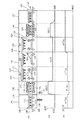
図1(a)に図示した装置は、前室101、ベーク処理室102、第1段目ゲッタ処理室103、電子線クリーニング処理室104、第2段目ゲッタ処理室105、封着処理室106及び冷却室107が順次搬送方向(図中の矢印127)に従って配列され、RP110とFP112は、搬送ローラ109及び搬送ベルト108の駆動によって、順次、矢印127方向に各部屋を通過し、この通過中に各種の処理が施される。つまり、前室101における真空雰囲気下での用意、ベーク処理室102におけるベーク処理、第1段目ゲッタ処理室における第1のゲッタ処理、電子線クリーニング処理室104における電子線照射によるクリーニング、第2段目ゲッタ処理室105における第2のゲッタ処理、封着処理室106における加熱封着及び冷却室107における冷却処理の各工程が直列された一ライン上で行われるものとなっている。
【0028】
上記各部屋間には、例えばアルミニウム、クロム、ステンレスなどの反射性金属によって形成した熱遮蔽部材128(板形状、フィルム形状など)が配置されているのが好ましい。この熱遮蔽部材128は、図1(b)に図示する温度プロファイルの温度が相違する部屋間、例えば、ベーク処理室102と第1段目ゲッタ処理室103との間と、第2段目ゲッタ処理室105と封着処理室106との間のいずれか一方、最適には両者に配置するのが好ましいが、各部屋間毎に配置してもよい。また、上記熱遮蔽部材128は、搬送ベルト108上に載置したFP112と昇降器117に固定したRP110とが各室間の移動する際に、障害を与えないように設置される。
【0029】
図1(a)に図示した装置の前室101とベーク処理室102との間にはロードロック129が配置されている。ロードロック129は前室101とベーク処理室102間を開閉するものである。また、前室101には真空排気系130が接続されており、ベーク処理室102には真空排気系131が接続されている。
【0030】
RP110とFP112とを前室101に搬入した後、搬入口110を遮蔽し、同時にロードロック129を遮蔽し、この前室101の内部を真空排気系130によって真空排気する。この間、ベーク処理室102、第1段目ゲッタ処理室103、電子線クリーニング処理室104、第2段目ゲッタ処理室105、封着処理室106及び冷却室107の全内部を真空排気系131によって真空排気して真空排気状態とする。
【0031】
上記前室101と、その後の各部屋が真空排気状態に達したとき、ロードロック129を開放し、RP110とFP112とを前室101から搬出してベーク処理室102に搬入し、この搬入終了後にロードロック129を遮断してから搬入口110を開けて、再度別のRP110とFP112とを前室101に搬入し、前室101の内部を真空排気系130によって真空排気する工程を繰り返す。
【0032】
本発明においては、上記したロードロック129と同じロードロック(図示せず)を各部屋間に配置しておくことが好ましい。このロードロックは、各部屋間毎であってもよいが、このロードロックを図1(c)に図示する真空度プロファイルの真空度が相違する部屋間毎、例えば、ベーク処理室102と第1段目ゲッタ処理室103との間と、電子線クリーニング室104と第2段目ゲッタ処理室105との間のいずれか一方、最適には両者に配置するのが好ましい。
【0033】
本発明では、前室101に搬入する前のRP111に、予め、真空構造をシールする外囲器113及び耐大気圧構造を形成するスペーサ115を固定設置しておくことが好ましい。FP112の上記外囲器113に対応した位置には、フリットガラスなどの低融点物質やインジウムなどの低融点金属又はその合金を用いた封着材114を設けることができる。また、図示するとおり、上記封着材114を外囲器113に設けることも可能である。
【0034】
大気に曝されることなくベーク処理室102に搬入されてきたRP111とFP112とには、このベーク処理室102内で、加熱プレート116の加熱処理(ベーク処理)が施される。このベーク処理によって、RP111とFP112に含有されている水素ガス、水蒸気、酸素などの不純物ガスを排出させることができる。このときのベーク温度は、一般的に、300℃〜400℃、好ましくは350℃〜380℃である。このときの真空度は約10-4Paである。
【0035】
ベーク処理を終了したRP111とFP112とを第1段目ゲッタ処理室103に搬入させ、RP111をホルダー118に固定し、昇降器117によって部屋103の上部へ移動させ、FP112に対してゲッタフラッシュ装置119内に内蔵させていた蒸発可能ゲッタ材(例えば、バリウムなどのゲッタ材)のゲッタ材フラッシュ120を生じさせ、FP112表面にバリウム膜などからなるゲッタ膜(図示せず)を付着せしめる。この際の第1段目ゲッタの膜厚は、一般的に5nm〜500nm、好ましくは10nm〜100nm、より好ましくは、20nm〜200nmである。また、本発明では、上記ゲッタ材のほかに、RP111又はFP112上に、予め、チタン材やNEG材などからなるゲッタ膜又はゲッタ部材を設けておいてもよい。
【0036】
上記ホルダー118は、RP111が脱落することなく十分な力で固定することができる機材、例えば、静電チャック方式や真空着チャック方式を利用した機材を用いることができる。
【0037】
ホルダー118に固定されたRP111は、昇降器117によって、搬送ベルト108上のFP112から十分に離れた位置まで上昇させる。この際のRP111とFP112との間隔は、用いた真空室のサイズにもよるが、両基板間のコンダクタンスを十分小さくするに十分な間隔とするのがよい。この際の両基板間の間隔は、一般的には、5cm以上とすれば十分である。
【0038】
また、上記工程において、バリウムゲッタを用いた場合では、第1段目ゲッタ処理室103のプロセス温度は、約100℃に設定される。このときの真空度は、10-5Paである。
【0039】
図においてゲッタフラッシュ120を照射しているのはFP112のみとなっているが、本発明では、RP111のみもしくはRP111とFP112の両者に対して上記同様のゲッタフラッシュ120を照射してゲッタを付与することも可能である。また、第1のゲッタフラッシュは、前記ベーク処理室102におけるベーク処理又は処理後の真空雰囲気の真空度を高めるために、前記ベーク処理室102内で行うこともできる。
【0040】
続いて、RP111とFP112とを、電子線クリーニング処理室104に大気に曝すことなく搬入し、この電子線クリーニング処理室104でRP111及び/又はFP112に対して電子線発振器121より電子線122を走査し、特にFP112の蛍光体(図示せず)中の不純物ガスを放出させる上記搬入の際、昇降器117に保持したRP111と搬送ベルト108に保持したFP112との間隔は、前の第1段目ゲッタ処理工程での間隔をそのまま維持するのがよい。
【0041】
図において電子線クリーニング処理を行っているのはFP112のみとなっているが、本発明では、RP111のみもしくはRP111とFP112の両者に対して上記同様の電子線クリーニング処理を施すことも可能である。
【0042】
上記電子線クリーニング処理の後、RP111とFP112を大気に曝すことなく第2段目ゲッタ処理室105に搬入し、そこで前記第1段目ゲッタ処理室103と同様の方法で、ゲッタフラッシュ装置123からゲッタフラッシュ124を生じさせ、FP112に対してゲッタを付与する。この際の第2段目ゲッタの膜厚は、一般的に5nm〜500nm、好ましくは10nm〜100nm、より好ましくは、20nm〜200nmである。上記搬入の際、昇降器117に保持したRP111と搬送ベルト108に保持したFP112との間隔は、前の第1段目ゲッタ処理工程での間隔をそのまま維持するのがよい。また、第2段目ゲッタは第1段目ゲッタと同様にRP111にのみ付与したり、FP112とRP111の両者に付与することもができる。
【0043】
上記第2段目のゲッタが付与されたFP112と昇降器117によって第2段目ゲッタ室105の上部に位置していたRP111を下降させ、大気に曝すことなく次の封着処理室106に搬入させる。この際、RP111とFP112とをそれぞれの基板上に設けているマトリクス配置した電子線放出素子と蛍光体とを内側に向けた状態で、スペーサ115及び外囲器113が互いに接するまで対向配置するよう、昇降器117を動作させる。
【0044】
封着処理室106内の相対向配置したRP111とFP112とに対して加熱プレート125を作用させ、予め設けておいた封着材114がインジウムのような低融点金属の場合では、低融点金属が溶融するまで加熱し、また封着材114がフリットガラスのような非金属の低融点物質の場合には、低融点物質が感化し接着性を帯びる温度まで加熱する。図1(b)では、封着材114としてインジウムを用いた例として、180℃の温度に設定されている。
【0045】
上記封着処理室106の真空度を10-6Pa以上の高真空度に設定することができる。このためRP111とFP112と外囲器113とで密封された表示パネル内部の真空度についても、10-6Pa以上の高真空度に設定することができる。
【0046】
上記封着処理室106にて作成した表示パネルは、次の冷却室107に搬出され、ゆっくり冷却される。
【0047】
本発明の装置は、上記封着室106と冷却室107との間に、上記ロードロック29と同様のロードロック(図示せず)を設け、該ロードロック開放時に封着処理室106から表示パネルを搬出させ、冷却室107に搬入後、該ロードロックを遮蔽し、ここで徐冷後、搬出口126を開放し、表示パネルを冷却室107から搬出させ、最後に該搬出口126を遮蔽して、全工程を終了する。また、次の工程の開始前に、冷却室107の内部を独立配置した真空排気系(図示せず)によって、真空状態に設定しておくのがよい。
【0048】
また、本発明は、上記各室及101〜107をアルゴンガス、ネオンガスなどの不活性ガス又は水素ガスを減圧下で含有させることができる。
【0049】
上記の例はベストモードであるが、第1の変形例として、前室101における真空雰囲気下での用意、第1段目ゲッタ処理室における第1のゲッタ処理、封着処理室106における加熱封着、冷却室107における冷却処理の順に工程を進めるように各部屋を直列させる例が挙げられる。
【0050】
第2の変形例としては、前室101における真空雰囲気下での用意、ベーク処理室102におけるベーク処理、封着処理室106における加熱封着、冷却室107における冷却処理の順に工程を進めるように各部屋を直列させる例が挙げられる。
【0051】
第3の変形例としては、前室101における真空雰囲気下での用意、ベーク処理室102におけるベーク処理、第1段目ゲッタ処理室における第1のゲッタ処理、封着処理室106における加熱封着及び冷却室107における冷却処理の順に工程を進めるように各部屋を直列させる例が挙げられる。
【0052】
第4の変形例としては、RP111とFP112を別々の搬送手段で搬送できるようにすることが挙げられる。
【0053】
図2は、前室201、ベーク処理室202、第1段目ゲッタ処理室203、電子線クリーニング処理室204、第2段目ゲッタ処理室205、封着処理室206及び冷却室207を中心真空室208の周りにスター配置上に設けた装置の模式平面図である。各部屋201〜207は、各々独立の部屋で仕切られている。
【0054】
図2の装置において、前室201と中心真空室208との間に、ロードロック209が設けられているが、他の部屋202〜207にも同様のロードロックを用い、全室201〜207と中心真空室208との間をロードロックで仕切ることができる。また、ベーク処理室202と中心真空室208との間に設けたロードロックに変えて、熱遮蔽部材210を用いることもできる。また、同様に、他の部屋203〜207と中心真空室208との間に設けたロードロックに変えて、熱遮蔽部材210を用いることもできる。
【0055】
中心真空室208には、搬送ハンド211が設置され、その両端部に、RP111とFP112とを静電チャック方式又は真空チャック方式によって固定可能とした搬送ハンド213が設置されている。この搬送ハンド213は、回転軸212を中心にそれぞれ矢印214の方向に回転可能とした搬送棒211に設置されている。
【0056】
搬送ハンド213の動作によって、RP111とFP112を各部屋201〜207毎に搬入及び搬出を繰り返すことによって、各部屋ごとで、各処理工程が施される。この際、RP111とFP112の両基板ごとに全処理工程を施してもよいが、好ましくは、RP111とFP112の両基板のうち、一方の基板の基板のみを所定の工程のみを処理するのがよい。例えば、RP111とFP112の両基板を上記の如く全工程を処理するのに変えて、FP112のみを第1段目ゲッタ処理室203及び第2段目ゲッタ処理室205に搬入せしめ、そこで、FP112についてのみゲッタ処理を施し、この間、RP111は、中心真空室208内に待機させ、RP111に対するゲッタ処理を省略することも可能である。
【0057】
また、本発明は、上記各室及201〜207及び中心真空室208内をアルゴンガス、ネオンガスなどの不活性ガス又は水素ガスを減圧下で含有させることができる。
【0058】
図3は、本発明の装置及び方法を用いて作成した画像表示装置の断面図である。図4は、その斜視図である。
【0059】
図中、図1及び図2と同一符号は、同一部材である。上記装置及び方法によって作成した画像表示装置は、RP111とFP112と外囲器113とによって真空容器又は減圧容器が形成されている。上記減圧容器内には、アルゴンガス、ネオンガスなどの不活性ガス又は水素ガスを減圧下で含有することができる。
【0060】
また、真空容器の場合には、10-5Pa以上、好ましくは、10-6Pa以上の高真空に設定することができる。
【0061】
上記真空容器又は減圧容器内には、スペーサ115が配置さて耐大気圧構造を形成している。本発明で用いたスペーサ115は、無アルカリガラスなどの無アルカリ絶縁物質からなる本体311と、該本体311の表面を覆って配置した高抵抗物質で成膜された高抵抗膜309と両端に設けた金属(タングステン、銅、銀、金、モリブデンやこれらの合金など)膜308及び310とを有し、配線306上に導電性接着剤を介して電気的に接続接着されている。スペーサ115は、上記前室101又は201に搬入する際には、前もってRP111にフリットガラスなどの低融点接着剤307によって接着固定され、封着処理室106又は206において処理が終了した時点で、上記スペーサ115のもう一方の端部とFP12とは電気的に接続されて接して配置される。
【0062】
RP111は、ガラスなどの透明基板304と、ナトリウムなどのアルカリの侵入を防止するための下地膜(SiO2、SnO2など)305と、XYマトリクス配列した複数の電子線放出素子312とが配置されている。配線306は、電子線放出素子と接続したカソード側XYマトリクス配線の一方のカソード側配線を構成する。
【0063】
本発明は、蛍光体励起手段又は画像表示素子部材として用いた電子線放出素子312に変えて、プラズマ発生素子を用いることができる。この際、容器内には、アルゴンガス、ネオンガスなどの不活性ガス又は水素ガスを減圧下で含有させる。
【0064】
FP112は、ガラスなどの透明基板301と蛍光体層302とアノード源(図示せず)に接続したアノード金属(アルミニウム、銀、銅など)膜303とが配置されている。
【0065】
また、本発明は、上記プラズマ発生素子を用いた際には、画像表示用部材として用いた蛍光体に変えて、カラーフィルターを用いることができる。
【0066】
外囲器113は、上記前室101又は201に搬入する際には、前もってRP111にフリットガラスなどの低融点接着剤313によって接着固定しておき、上記封着処理室106又は206における処理工程で、インジウムやフリットガラスを用いた封着材114によって固定接着されている。
【0067】
【発明の効果】
本発明によれば、上記電子放出素子やプラズマ発生素子をXY方向に100万画素以上のように大容量で設け、且つこの大容量画素を対角サイズ30インチ以上の大画面に設けた画像表示装置を製造するに当たって、製造工程時間を大幅に短縮することができたのと同時に、画像表示装置を構成する真空容器を10-6Pa以上のような高真空に達成させることができた。
【図面の簡単な説明】
【図1】本発明の一例に係る第1の装置の模式的断面図である。
【図2】本発明の他の例に係る第2の装置の模式的平面図である。
【図3】本発明の装置及び方法によって製造された画像表示装置の断面図である。
【符号の説明】
101 前室
102 ベーク処理室
103 第1段目ゲッタ処理室
104 電子線クリーニング処理室
105 第2段目ゲッタ処理室
106 封着処理室
107 冷却室
108 搬送ベルト
109 搬送ローラ
110 搬入口
111 リヤープレート(RP)
112 フェースプレート(FP)
113 外囲器
114 封着材
115 スペーサ
116 加熱プレート
117 昇降器
118 ホルダー
119 ゲッタフラッシュ装置
120 ゲッタフラッシュ
121 電子線発振器
122 電子線
123 ゲッタフラッシュ装置
124 ゲッタフラッシュ
125 加熱プレート
126 搬出口
127 進行方向矢印
128 熱遮蔽部材
129 ロードロック
130 真空排気系
131 真空排気系
201 前室
202 ベーク処理室
203 第1段目ゲッタ処理室
204 電子線クリーニング処理室
205 第2段目ゲッタ処理室
206 封着処理室
207 冷却室
208 中心真空室
209 ロードロック
210 熱遮蔽部材
211 回転棒
212 回転軸
213 搬送ハンド
214 回転方向矢印[0001]
[Technical field to which the invention belongs]
The present invention provides an image display device in which electron-emitting devices are arranged in a matrix, and in particular, a rear plate (RP) provided with electron-emitting devices arranged in a matrix as a first image forming member and a phosphor as a second image forming member. relates to the preparation of the image display device having a face plate (FP) and a display panel disposed facing the.
[0002]
[Prior art]
2. Description of the Related Art Conventionally, two types of electron-emitting devices, known as a thermionic electron-emitting device and a cold cathode electron-emitting device, are known. Cold cathode electron-emitting devices include field emission type (hereinafter referred to as FE type), metal / insulating layer / metal type (hereinafter referred to as MIM type), surface conduction type electron emitting device, and the like.
[0003]
As an example of the FE type, W.W. P. Dyke & W. W. Dolan, “Field Emission”, Advance in Electro Physics, 8, 89 (1956), or C.I. A. Spindt, “PHYSICAL Properties of Thin-Film Field Emission Catalysts with Mollybdenum Cones”, J. Am. Appl. Phys. 47, 5248 (1976), etc. are known.
[0004]
Examples of the MIM type include C.I. A. Mead, “Operation of Tunnel-Emission Devices”, J. Am. Appl. Phys. , 32, 646 (1961), etc. are known.
[0005]
Examples of the surface conduction electron-emitting device type include M.I. I. Elinson, Radio Eng. Electron Phys. , 10, 1290 (1965).
[0006]
The surface conduction electron-emitting device utilizes a phenomenon in which electron emission occurs when a current flows in parallel to a film surface of a small-area thin film formed on a substrate. As this surface conduction electron-emitting device, one using the SnO 2 thin film by Erinson et al., One using Au thin film [G. Dittmer: “Thin Solis Films,” 9,317 (1972)], In 2 O 3 / SnO 2 thin film [M. Hartwell and C.H. G. Fonstad: “IEEE Trans. ED Conf.”, 519 (1975)], carbon thin film [Hisa Araki et al .: Vacuum, Vol. 26, No. 1, pp. 22 (1983)] have been reported.
[0007]
In the manufacture of an image display apparatus using the above-described electron-emitting devices, an electron source substrate in which these electron-emitting devices are arranged in a matrix is prepared as RP, and a phosphor that emits light upon being excited by an electron beam is provided. Prepare a phosphor substrate to be an FP, and arrange an envelope providing a vacuum seal structure and a spacer providing an atmospheric pressure resistant structure so that the electron-emitting device and the phosphor are inside. Then, after these FP and RP are arranged to face each other, the inside is sealed using a low melting point material such as frit glass or indium as a sealing material, and the inside is evacuated from a vacuum exhaust pipe provided in advance. A manufacturing process in which a vacuum exhaust pipe is sealed to form a display panel is used.
[0008]
The above-described manufacturing method according to the prior art requires a very long time to manufacture one display panel. For example, for manufacturing a display panel having an internal vacuum of 10 −6 Pa or more. Was not suitable.
[0009]
This problem of the prior art has been solved by, for example, the method described in JP-A-11-135018.
[0010]
[Problems to be solved by the invention]
Since the method described in the above Japanese Patent Application Laid-Open No. 11-135018 uses only the step of sealing the two substrates after aligning the FP and RP in a single vacuum chamber, Steps such as baking, gettering, and electron beam cleaning, which are other steps necessary for creating the display panel described above, also require processing in a single vacuum chamber. Since the movement of each RP between the vacuum chambers is performed by breaking the atmosphere, each vacuum chamber is evacuated every time FP and RP are carried in, and therefore the manufacturing process time is long. At the same time that shortening was required, it was also required to achieve a high vacuum such as a degree of vacuum of 10 −6 Pa or higher in the display panel in the final manufacturing process in a short time.
[0011]
The present invention has been made in view of the above-described conventional problems, and it is an object of the present invention to make it possible to easily shorten the evacuation time and increase the degree of vacuum in the manufacture of an image display device, thereby improving the manufacturing efficiency. To do.
[0012]
[Means for Solving the Problems]
The present invention (reference) , first,
In the manufacturing method of the image display device,
a: preparing a first substrate on which a phosphor excitation means is arranged and a second substrate on which a phosphor emitting light by the phosphor excitation means is arranged in a vacuum atmosphere;
b: One or both of the first substrate and the second substrate are loaded into a getter processing chamber in a vacuum atmosphere under a vacuum atmosphere, and one of the loaded substrates or both loaded substrates or Gettering both substrates, and
c: The image display device manufacturing method includes a step of carrying the first substrate and the second substrate into a sealing treatment chamber in a vacuum atmosphere in a vacuum atmosphere and heat-sealing in a facing state.
[0013]
Secondly, the present invention (reference)
In the manufacturing method of the image display device,
a: preparing a first substrate on which a phosphor excitation means is arranged and a second substrate on which a phosphor emitting light by the phosphor excitation means is arranged in a vacuum atmosphere;
b: carrying the first substrate and the second substrate into a bake processing chamber in a vacuum atmosphere under a vacuum atmosphere and baking both the substrates at a predetermined temperature; and
c: The image display device manufacturing method includes a step of carrying the first substrate and the second substrate into a sealing treatment chamber in a vacuum atmosphere in a vacuum atmosphere and heat-sealing in a facing state.
[0014]
Third, the present invention
In the manufacturing method of the image display device,
a: preparing a first substrate on which a phosphor excitation means is arranged and a second substrate on which a phosphor emitting light by the phosphor excitation means is arranged in a vacuum atmosphere;
b: carrying the first substrate and the second substrate into a bake processing chamber in a vacuum atmosphere under a vacuum atmosphere, and baking the both substrates at a predetermined temperature;
c: One or both of the first substrate and the second substrate are loaded into a getter processing chamber in a vacuum atmosphere under a vacuum atmosphere, and one or both of the loaded substrate and both loaded substrates are loaded. A step of gettering the substrate of
d: A method of manufacturing an image display device having a step of carrying the first substrate and the second substrate into a sealing processing chamber in a vacuum atmosphere in a vacuum atmosphere and heat-sealing in a facing state.
[0015]
The present invention fourthly,
In the manufacturing method of the image display device,
a: preparing a first substrate on which a phosphor excitation means is arranged and a second substrate on which a phosphor emitting light by the phosphor excitation means is arranged in a vacuum atmosphere;
b: carrying the first substrate and the second substrate into a bake processing chamber in a vacuum atmosphere under a vacuum atmosphere, and baking the both substrates at a predetermined temperature;
c: One or both of the first substrate and the second substrate are loaded into a first getter processing chamber in a vacuum atmosphere under a vacuum atmosphere, and one of the loaded substrates or both loaded substrates is loaded. Or first gettering both substrates;
d: One or both of the first substrate and the second substrate are loaded into an electron beam cleaning processing chamber in a vacuum atmosphere under a vacuum atmosphere, and one of the loaded substrates or both loaded substrates is loaded. Or a process of cleaning both substrates by electron beam irradiation,
e: One or both of the first substrate and the second substrate are loaded into a second getter processing chamber in a vacuum atmosphere in a vacuum atmosphere, and one of the loaded substrates or both loaded substrates is loaded. Or second gettering both substrates;
f: A feature of the method for manufacturing an image display device is the step of carrying the first substrate and the second substrate into a sealing treatment chamber in a vacuum atmosphere in a vacuum atmosphere and heat-sealing in a facing state.
[0016]
The present invention (reference) , fifth,
In an apparatus for manufacturing an image display device,
a: Conveying means for conveying the first substrate provided with the first image display device member and the second substrate provided with the second image display device member;
b: a first vacuum chamber in which one or both of the first substrate and the second substrate can be carried in a vacuum atmosphere by the transfer means;
c: a getter applying means having a getter precursor disposed in the first vacuum chamber and a getter activating means for activating the getter precursor;
d: a second vacuum chamber in which the first substrate and the second substrate can be carried in a vacuum atmosphere by the transfer means;
e: The first substrate and the second substrate disposed in the second vacuum chamber are directed inward, and the first substrate and the second substrate are opposed to each other. An image display device having a sealing means for heat-sealing the first substrate and the second substrate, which are arranged in the second vacuum chamber and are opposed to each other by the substrate positioning means, at a predetermined temperature; The manufacturing equipment is characterized.
[0017]
The present invention (reference) is sixth,
In an apparatus for manufacturing an image display device,
a: Conveying means for conveying the first substrate provided with the first image display device member and the second substrate provided with the second image display device member;
b: a first vacuum chamber in which the first substrate and the second substrate can be carried in a vacuum atmosphere by the transfer means;
c: a baking means for heating the first substrate and the second substrate carried in and disposed in the first vacuum chamber, and baking the first substrate and the second substrate;
d: a second vacuum chamber in which the first substrate and the second substrate can be carried in a vacuum atmosphere by the transfer means;
e: The first substrate and the second substrate disposed in the second vacuum chamber are directed inward, and the first substrate and the second substrate are opposed to each other. An image display device having a sealing means for heat-sealing the first substrate and the second substrate, which are arranged in the second vacuum chamber and are opposed to each other by the substrate positioning means, at a predetermined temperature; The manufacturing equipment is characterized.
[0018]
Seventh, the present invention (reference)
In an apparatus for manufacturing an image display device,
a: Conveying means for conveying the first substrate provided with the first image display device member and the second substrate provided with the second image display device member;
b: a first vacuum chamber in which the first substrate and the second substrate can be carried in a vacuum atmosphere by the transfer means;
c: a baking means for heating the first substrate and the second substrate carried in and disposed in the first vacuum chamber, and baking the first substrate and the second substrate;
d: a second vacuum chamber in which one or both of the first substrate and the second substrate can be carried in a vacuum atmosphere by the transfer means;
e: a getter applying means having a getter precursor disposed in the second vacuum chamber and a getter activating means for activating the getter precursor;
f: a third vacuum chamber in which the first substrate and the second substrate can be carried in a vacuum atmosphere by the transfer means;
g: The first substrate and the second image display device member disposed in the third vacuum chamber are directed inward so that the first substrate and the second substrate face each other. An image display device comprising: a substrate disposing unit; and h: a sealing unit disposed in the third vacuum chamber, wherein the first substrate and the second substrate opposed to each other by the substrate disposing unit are heated and sealed at a predetermined temperature The manufacturing equipment is characterized.
[0019]
The present invention (reference) , eighth,
In an apparatus for manufacturing an image display device,
a: Conveying means for conveying the first substrate provided with the first image display device member and the second substrate provided with the second image display device member;
b: a first vacuum chamber in which the first substrate and the second substrate can be carried in a vacuum atmosphere by the transfer means;
c: a baking means for heating the first substrate and the second substrate carried in and disposed in the first vacuum chamber, and baking the first substrate and the second substrate;
d: a second vacuum chamber in which one or both of the first substrate and the second substrate can be carried in a vacuum atmosphere by the transfer means;
e: a first getter applying means having a getter precursor disposed in the second vacuum chamber and a getter activating means for activating the getter precursor;
f: a third vacuum chamber in which one or both of the first substrate and the second substrate can be carried in a vacuum atmosphere by the transfer means;
g: an electron beam cleaning means disposed in the third vacuum chamber for performing an electron beam cleaning process by irradiating an electron beam;
h: a fourth vacuum chamber in which one or both of the first substrate and the second substrate can be carried in a vacuum atmosphere by the transfer means;
i: a second getter applying means having a getter precursor disposed in the fourth vacuum chamber and a getter activating means for activating the getter precursor;
j: a fifth vacuum chamber in which the first substrate and the second substrate can be carried in a vacuum atmosphere by the transfer means;
k: The first substrate and the second image display device member, which are arranged in the fifth vacuum chamber, face inward, and the first substrate and the second substrate are arranged to face each other. A substrate placement means; and l: an image display device having a sealing means placed in the fifth vacuum chamber, wherein the first substrate and the second substrate placed opposite to each other by the substrate placement means are heated and sealed at a predetermined temperature. There is a feature in the manufacturing equipment.
[0020]
The present invention (reference) is ninth,
a. Transport means for transporting the first substrate provided with the first image display device member and the second substrate provided with the second image display device member;
b. A first vacuum chamber capable of carrying in the first substrate carried in by the carrying means while maintaining a reduced pressure state without exposing to the atmosphere;
c. A getter applying means having a getter precursor disposed in the first decompression chamber and a getter activating means for activating the getter precursor;
d. A second decompression chamber capable of carrying the first substrate provided with a getter and the second substrate without exposing to the atmosphere;
e. A substrate arrangement in which the first image display device member and the second image display device member are arranged in the second decompression chamber so that the first substrate and the second substrate face each other. Means, and f. Sealing means for heating the first substrate and the second substrate disposed in the second decompression chamber so as to face each other by the substrate placing means at a predetermined temperature and sealing the first substrate and the second substrate; The image display apparatus manufacturing apparatus has a feature.
[0021]
The present invention (reference) , tenth,
a. Transport means for transporting the first substrate provided with the first image display device member and the second substrate provided with the second image display device member;
b. A first decompression chamber capable of carrying in the first substrate and the second substrate carried in by the carrying means while maintaining a reduced pressure state without being exposed to the atmosphere;
c. A getter applying means having a getter precursor carried into the first decompression chamber and a getter activating means for activating the getter precursor; and d. A second decompression chamber in which the first substrate and the second substrate in the first decompression chamber can be carried in without being exposed to the atmosphere;
e. A substrate arrangement in which the first image display device member and the second image display device member are arranged in the second decompression chamber so that the first substrate and the second substrate face each other. Means, and f. Sealing means for heating the first substrate and the second substrate disposed in the second decompression chamber so as to face each other by the substrate placing means at a predetermined temperature and sealing the first substrate and the second substrate; The image display apparatus manufacturing apparatus has a feature.
[0022]
The present invention (reference) , eleventh,
a. Transport means for transporting the first substrate provided with the first image display device member and the second substrate provided with the second image display device member;
b. A first vacuum chamber capable of carrying in the first substrate and the second substrate carried in by the carrying means while maintaining a reduced pressure state without being exposed to the atmosphere;
c. A baking means for applying heat to the first substrate and the second substrate that are carried in and disposed in the first decompression chamber, and baking the first substrate and the second substrate;
d. A getter precursor disposed in the first decompression chamber or another second decompression chamber that allows the first substrate or the second substrate to be loaded from the first decompression chamber without being exposed to the atmosphere, and the getter precursor First getter providing means having getter activating means for activating,
e. A third vacuum chamber capable of carrying in the first substrate or the second substrate without being exposed to the atmosphere from the first decompression chamber or the second decompression chamber;
f. A substrate arrangement in which the first image display device member and the second image display device member are disposed in the third decompression chamber so that the first substrate and the second substrate face each other. Means, and g. Sealing means for heating the first substrate and the second substrate disposed in the third decompression chamber facing each other by the substrate placement means at a predetermined temperature and sealing the first substrate and the second substrate; The image display apparatus manufacturing apparatus has a feature.
[0023]
In the twelfth aspect of the present invention (reference) ,
a. Transport means for transporting the first substrate provided with the first image display device member and the second substrate provided with the second image display device member;
b. A first decompression chamber capable of carrying in the first substrate and the second substrate carried in by the carrying means while maintaining a reduced pressure state without exposing to the atmosphere;
c. A baking means for applying heat to the first substrate and the second substrate that are carried in and disposed in the first decompression chamber, and baking the first substrate and the second substrate;
d. A getter precursor disposed in the first decompression chamber or another second decompression chamber that allows the first substrate or the second substrate to be loaded from the first decompression chamber without being exposed to the atmosphere, and the getter precursor First getter providing means having getter activating means for activating,
e. A third vacuum chamber capable of carrying in the first substrate or the second substrate from the first decompression chamber or the second decompression chamber without exposing to the atmosphere;
f. An electron beam cleaning means disposed in the third decompression chamber for cleaning the first substrate or the second substrate by irradiating the first substrate or the second substrate with an electron beam;
g. A fourth decompression chamber that can be carried in from the third decompression chamber without exposing the first substrate or the second substrate to the atmosphere;
h. A second getter applying means having a getter precursor disposed in the fourth decompression chamber and a getter activating means for activating the getter precursor;
i. A fifth vacuum chamber capable of carrying in the first substrate or the second substrate from the fourth decompression chamber without exposing to the atmosphere;
j. A substrate arrangement in which the first image display device member and the second image display device member are arranged inward in the fifth decompression chamber so that the first substrate and the second substrate face each other. Means, and k. Sealing means for heating the first substrate and the second substrate disposed in the fifth decompression chamber facing each other by the substrate placement means at a predetermined temperature and sealing the first substrate and the second substrate; The apparatus for manufacturing the image display apparatus has a feature.
[0024]
The present invention also provides:
In the first and second features, the steps a, b, and c are steps set on one line, and are formed of a reflective metal or the like between the getter processing chamber and the sealing processing chamber. A heat shielding member is disposed,
In the first and second features, the steps a, b, and c are steps set on one line, and a load lock is disposed between the getter processing chamber and the sealing processing chamber. thing,
In the first and second features, the steps a, b, and c are set on a star arrangement, and the getter processing chamber and the sealing processing chamber are separated by an independent chamber,
In the third feature, the steps a, b, c, and d are steps set on one line, between the bake chamber and the getter processing chamber, and between the getter processing chamber and the sealing processing chamber. Or a heat shielding member formed of a reflective metal or the like is disposed between the baking chamber, the getter processing chamber, and the sealing processing chamber,
In the third feature, the steps a, b, c, and d are steps set on one line, between the baking processing chamber and the getter processing chamber, between the getter processing chamber and the sealing processing chamber. A load lock is disposed between the bake chamber, the getter processing chamber and the sealing chamber,
In the third feature, the steps a, b, c, and d are set on a star arrangement, and the bake processing chamber, the getter processing chamber, and the sealing processing chamber are separated by independent chambers,
In the fourth feature, the steps a, b, c, d, e, and f are steps set on one line, and the first getter processing chamber is provided between the bake chamber and the first getter processing chamber. Between the electron beam cleaning processing chamber, the electron beam cleaning processing chamber and the second getter processing chamber, or between the second getter processing chamber and the sealing processing chamber. A shielding member is disposed;
In the fourth feature, the steps a, b, c, d, e and f are steps set on one line, and the first getter is disposed between the bake processing chamber and the first getter processing chamber. A load lock is disposed between the processing chamber and the electron beam cleaning processing chamber, between the electron beam cleaning processing chamber and the second getter processing chamber, or between the second getter processing chamber and the sealing processing chamber. ,
In the fourth feature, the steps a, b, c, d, e, and f are set on a star arrangement, the bake processing chamber, the first getter processing chamber, the electron beam cleaning processing chamber, and the second The getter processing chamber and the sealing processing chamber are separated by a separate room;
In the fifth and sixth features, the first vacuum chamber and the second vacuum chamber are arranged on one line,
In the fifth and sixth features, the first vacuum chamber and the second vacuum chamber are arranged on one line, and each chamber is partitioned by a heat shielding member formed of a reflective metal or the like. That
In the fifth and sixth features, the first vacuum chamber and the second vacuum chamber are provided on a star arrangement, and each room is partitioned by an independent room,
In the seventh feature, the first vacuum chamber, the second vacuum chamber, and the third vacuum chamber are arranged on one line, and each chamber is formed of a reflective metal or the like. Being partitioned by
In the seventh feature, the first vacuum chamber, the second vacuum chamber, and the third vacuum chamber are arranged on one line, and each chamber is partitioned by a load lock,
In the seventh feature, the first vacuum chamber, the second vacuum chamber, and the third vacuum chamber are provided on a star arrangement, and each room is partitioned by an independent room,
In the eighth feature, the first vacuum chamber, the second vacuum chamber, the third vacuum chamber, the fourth vacuum chamber, and the fifth vacuum chamber are arranged on one line, Each room is partitioned by a heat shielding member made of reflective metal, etc.
In the eighth feature, the first vacuum chamber, the second vacuum chamber, the third vacuum chamber, the fourth vacuum chamber, and the fifth vacuum chamber are arranged on one line, Each room is partitioned by a load lock,
In the eighth feature, the first vacuum chamber, the second vacuum chamber, the third vacuum chamber, the fourth vacuum chamber, and the fifth vacuum chamber are provided on a star arrangement. Each room is separated by a separate room,
Is included as a preferred embodiment thereof.
[0025]
Further, in the ninth to twelfth features, the first decompression chamber to the fifth decompression chamber contain an inert gas such as argon gas or neon gas or hydrogen gas under reduced pressure. In the ninth to twelfth features, the first image display device member is a plasma generating element, and the second image display device member is a phosphor or a color filter.
[0026]
DETAILED DESCRIPTION OF THE INVENTION
FIG. 1 (a) schematically shows a manufacturing apparatus according to the present invention, FIG. 1 (b) shows a temperature profile with the vertical axis relative to the horizontal axis time as the process temperature, and FIG. 1 (c) shows the horizontal axis time. It is a vacuum profile with the vertical axis representing the vacuum. Hereinafter, based on these, an example of the manufacturing method and the manufacturing apparatus according to the present invention will be described.
[0027]
The apparatus illustrated in FIG. 1A includes a
[0028]
It is preferable that a heat shielding member 128 (plate shape, film shape, or the like) formed of a reflective metal such as aluminum, chrome, or stainless steel is disposed between the rooms. The
[0029]
A
[0030]
After carrying in RP110 and FP112 in the
[0031]
When the
[0032]
In the present invention, the same load lock (not shown) as the above-described
[0033]
In the present invention, it is preferable that an
[0034]
The
[0035]
The
[0036]
The
[0037]
The
[0038]
In the above process, when a barium getter is used, the process temperature of the first stage
[0039]
In the figure, only the
[0040]
Subsequently, the
[0041]
In the figure, only the
[0042]
After the electron beam cleaning process, the
[0043]
The
[0044]
When the
[0045]
The degree of vacuum in the sealing
[0046]
The display panel created in the sealing
[0047]
In the apparatus of the present invention, a load lock (not shown) similar to the load lock 29 is provided between the sealing
[0048]
In the present invention, each of the
[0049]
Although the above example is the best mode, as a first modification, preparation in a vacuum atmosphere in the
[0050]
As a second modified example, the process proceeds in the order of preparation in a vacuum atmosphere in the
[0051]
As a third modified example, preparation in a vacuum atmosphere in the
[0052]
As a fourth modification, it is possible to transport the
[0053]
FIG. 2 shows a central vacuum in the
[0054]
In the apparatus of FIG. 2, a
[0055]
A
[0056]
By repeating the loading and unloading of the
[0057]
In the present invention, each of the
[0058]
FIG. 3 is a cross-sectional view of an image display apparatus created using the apparatus and method of the present invention. FIG. 4 is a perspective view thereof.
[0059]
In the figure, the same reference numerals as those in FIGS. 1 and 2 denote the same members. In the image display device created by the above apparatus and method, a vacuum container or a decompression container is formed by the
[0060]
In the case of a vacuum vessel, a high vacuum of 10 −5 Pa or higher, preferably 10 −6 Pa or higher can be set.
[0061]
A
[0062]
The
[0063]
In the present invention, a plasma generating element can be used instead of the electron
[0064]
The
[0065]
In the present invention, when the plasma generating element is used, a color filter can be used instead of the phosphor used as the image display member.
[0066]
When the
[0067]
【The invention's effect】
According to the present invention, the above-described electron-emitting device or plasma generating device is provided in a large capacity such as 1 million pixels or more in the XY direction, and the large capacity pixel is provided on a large screen having a diagonal size of 30 inches or more. In manufacturing the device, the manufacturing process time could be greatly shortened, and at the same time, the vacuum container constituting the image display device could be achieved at a high vacuum of 10 −6 Pa or more.
[Brief description of the drawings]
FIG. 1 is a schematic cross-sectional view of a first apparatus according to an example of the present invention.
FIG. 2 is a schematic plan view of a second device according to another example of the present invention.
FIG. 3 is a cross-sectional view of an image display device manufactured by the apparatus and method of the present invention.
[Explanation of symbols]
101
112 Face plate (FP)
113
Claims (12)
a:蛍光体励起手段を配置した第1基板及び蛍光体励起手段により発光する蛍光体を配置した第2基板を真空雰囲気下に用意する工程、
b:上記第1基板と第2基板を真空雰囲気のベーク処理室に真空雰囲気下で搬入し、該両方の基板を所定温度でベーク処理する工程、
c:上記第1基板と第2基板のうちの一方又は両方の基板を真空雰囲気のゲッタ処理室に真空雰囲気下で搬入し、搬入した一方の基板又は搬入した両方の基板のうちの一方又は両方の基板をゲッタ処理する工程、並びに、
d:上記第1基板と第2基板を真空雰囲気の封着処理室に真空雰囲気下で搬入して対向状態で加熱封着する工程
を有することを特徴とする画像表示装置の製造法。In the manufacturing method of the image display device,
a: preparing a first substrate on which a phosphor excitation means is arranged and a second substrate on which a phosphor emitting light by the phosphor excitation means is arranged in a vacuum atmosphere;
b: carrying the first substrate and the second substrate into a bake processing chamber in a vacuum atmosphere under a vacuum atmosphere, and baking the both substrates at a predetermined temperature;
c: One or both of the first substrate and the second substrate are loaded into a getter processing chamber in a vacuum atmosphere under a vacuum atmosphere, and one or both of the loaded substrate and both loaded substrates are loaded. A step of gettering the substrate of
d: A method for manufacturing an image display device, comprising the steps of: bringing the first substrate and the second substrate into a sealing treatment chamber in a vacuum atmosphere in a vacuum atmosphere and heat-sealing in a facing state.
a:蛍光体励起手段を配置した第1基板及び蛍光体励起手段により発光する蛍光体を配置した第2基板を真空雰囲気下に用意する工程、
b:上記第1基板と第2基板を真空雰囲気のベーク処理室に真空雰囲気下で搬入し、該両方の基板を所定温度でベーク処理する工程、
c:上記第1基板と第2基板のうちの一方又は両方の基板を真空雰囲気の第1ゲッタ処理室に真空雰囲気下で搬入し、搬入した一方の基板又は搬入した両方の基板のうちの一方又は両方の基板を第1ゲッタ処理する工程、
d:上記第1基板と第2基板のうちの一方又は両方の基板を真空雰囲気の電子線クリーニング処理室に真空雰囲気下で搬入し、搬入した一方の基板又は搬入した両方の基板のうちの一方又は両方の基板を電子線照射による電子線クリーニング処理する工程、
e:上記第1基板と第2基板のうちの一方又は両方の基板を真空雰囲気の第2ゲッタ処理室に真空雰囲気下で搬入し、搬入した一方の基板又は搬入した両方の基板のうちの一方又は両方の基板を第2ゲッタ処理する工程、
f:上記第1基板と第2基板を真空雰囲気の封着処理室に真空雰囲気下で搬入して対向状態で加熱封着する工程
を有することを特徴とする画像表示装置の製造法。In the manufacturing method of the image display device,
a: preparing a first substrate on which a phosphor excitation means is arranged and a second substrate on which a phosphor emitting light by the phosphor excitation means is arranged in a vacuum atmosphere;
b: carrying the first substrate and the second substrate into a bake processing chamber in a vacuum atmosphere under a vacuum atmosphere, and baking the both substrates at a predetermined temperature;
c: One or both of the first substrate and the second substrate are loaded into a first getter processing chamber in a vacuum atmosphere under a vacuum atmosphere, and one of the loaded substrates or both loaded substrates is loaded. Or first gettering both substrates;
d: One or both of the first substrate and the second substrate are loaded into an electron beam cleaning processing chamber in a vacuum atmosphere under a vacuum atmosphere, and one of the loaded substrates or both loaded substrates is loaded. Or a process of cleaning both substrates by electron beam irradiation,
e: One or both of the first substrate and the second substrate are loaded into a second getter processing chamber in a vacuum atmosphere in a vacuum atmosphere, and one of the loaded substrates or both loaded substrates is loaded. Or second gettering both substrates;
f: A method for manufacturing an image display device, comprising the steps of: bringing the first substrate and the second substrate into a sealing treatment chamber in a vacuum atmosphere in a vacuum atmosphere and heat-sealing in a facing state.
Priority Applications (11)
| Application Number | Priority Date | Filing Date | Title |
|---|---|---|---|
| JP2000038603A JP3754859B2 (en) | 2000-02-16 | 2000-02-16 | Manufacturing method of image display device |
| US09/781,305 US6905384B2 (en) | 2000-02-16 | 2001-02-13 | Method and apparatus for manufacturing image displaying apparatus |
| TW090103292A TW514960B (en) | 2000-02-16 | 2001-02-14 | Method and apparatus for manufacturing image displaying apparatus |
| AT01301315T ATE438195T1 (en) | 2000-02-16 | 2001-02-15 | METHOD AND DEVICE FOR PRODUCING AN IMAGE DISPLAY DEVICE |
| DE60139358T DE60139358D1 (en) | 2000-02-16 | 2001-02-15 | Method and apparatus for producing an image display device |
| EP01301315A EP1126496B1 (en) | 2000-02-16 | 2001-02-15 | Method and apparatus for manufacturing image displaying apparatus |
| KR10-2001-0007695A KR100442214B1 (en) | 2000-02-16 | 2001-02-16 | Method and apparatus for manufacturing image displaying apparatus |
| CNB011168730A CN100430981C (en) | 2000-02-16 | 2001-02-16 | Method and apparatus for making picture display device |
| KR10-2004-0019042A KR100441388B1 (en) | 2000-02-16 | 2004-03-19 | Method and apparatus for manufacturing image displaying apparatus |
| US11/101,506 US7226335B2 (en) | 2000-02-16 | 2005-04-08 | Method and apparatus for manufacturing image displaying apparatus |
| US11/620,819 US7628670B2 (en) | 2000-02-16 | 2007-01-08 | Method and apparatus for manufacturing image displaying apparatus |
Applications Claiming Priority (1)
| Application Number | Priority Date | Filing Date | Title |
|---|---|---|---|
| JP2000038603A JP3754859B2 (en) | 2000-02-16 | 2000-02-16 | Manufacturing method of image display device |
Related Child Applications (1)
| Application Number | Title | Priority Date | Filing Date |
|---|---|---|---|
| JP2005315794A Division JP4235640B2 (en) | 2005-10-31 | 2005-10-31 | Image display device manufacturing device |
Publications (3)
| Publication Number | Publication Date |
|---|---|
| JP2001229828A JP2001229828A (en) | 2001-08-24 |
| JP2001229828A5 JP2001229828A5 (en) | 2005-03-17 |
| JP3754859B2 true JP3754859B2 (en) | 2006-03-15 |
Family
ID=18562315
Family Applications (1)
| Application Number | Title | Priority Date | Filing Date |
|---|---|---|---|
| JP2000038603A Expired - Fee Related JP3754859B2 (en) | 2000-02-16 | 2000-02-16 | Manufacturing method of image display device |
Country Status (8)
| Country | Link |
|---|---|
| US (3) | US6905384B2 (en) |
| EP (1) | EP1126496B1 (en) |
| JP (1) | JP3754859B2 (en) |
| KR (2) | KR100442214B1 (en) |
| CN (1) | CN100430981C (en) |
| AT (1) | ATE438195T1 (en) |
| DE (1) | DE60139358D1 (en) |
| TW (1) | TW514960B (en) |
Families Citing this family (46)
| Publication number | Priority date | Publication date | Assignee | Title |
|---|---|---|---|---|
| JP3754859B2 (en) * | 2000-02-16 | 2006-03-15 | キヤノン株式会社 | Manufacturing method of image display device |
| US6848961B2 (en) * | 2000-03-16 | 2005-02-01 | Canon Kabushiki Kaisha | Method and apparatus for manufacturing image displaying apparatus |
| JP3754883B2 (en) * | 2000-03-23 | 2006-03-15 | キヤノン株式会社 | Manufacturing method of image display device |
| US7052354B2 (en) * | 2002-08-01 | 2006-05-30 | Canon Kabushiki Kaisha | Method for producing spacer and spacer |
| JP5068924B2 (en) * | 2004-02-20 | 2012-11-07 | 中外炉工業株式会社 | Continuous sealing processing furnace and sealing processing method for glass panel assembly |
| US7271529B2 (en) | 2004-04-13 | 2007-09-18 | Canon Kabushiki Kaisha | Electron emitting devices having metal-based film formed over an electro-conductive film element |
| JP4393257B2 (en) * | 2004-04-15 | 2010-01-06 | キヤノン株式会社 | Envelope manufacturing method and image forming apparatus |
| JP2006085933A (en) | 2004-09-14 | 2006-03-30 | Toshiba Matsushita Display Technology Co Ltd | Manufacturing method and manufacturing device of display device |
| US20060269656A1 (en) * | 2005-05-26 | 2006-11-30 | Eastman Kodak Company | Reducing contamination in OLED processing systems |
| JP2007027018A (en) * | 2005-07-21 | 2007-02-01 | Hitachi Ltd | Manufacturing method of display panel, and anode panel |
| US7710035B2 (en) | 2006-08-10 | 2010-05-04 | Lg Electronics Inc. | Plasma display apparatus omitting an exhaust unit |
| JP2010086947A (en) | 2008-09-02 | 2010-04-15 | Canon Inc | Method of manufacturing vacuum airtight container |
| JP2010135312A (en) | 2008-11-04 | 2010-06-17 | Canon Inc | Method of manufacturing airtight container |
| JP5620146B2 (en) | 2009-05-22 | 2014-11-05 | 三星ディスプレイ株式會社Samsung Display Co.,Ltd. | Thin film deposition equipment |
| JP5623786B2 (en) * | 2009-05-22 | 2014-11-12 | 三星ディスプレイ株式會社Samsung Display Co.,Ltd. | Thin film deposition equipment |
| KR101074792B1 (en) * | 2009-06-12 | 2011-10-19 | 삼성모바일디스플레이주식회사 | Apparatus for thin layer deposition |
| KR101117719B1 (en) | 2009-06-24 | 2012-03-08 | 삼성모바일디스플레이주식회사 | Apparatus for thin layer deposition |
| JP5328726B2 (en) * | 2009-08-25 | 2013-10-30 | 三星ディスプレイ株式會社 | Thin film deposition apparatus and organic light emitting display device manufacturing method using the same |
| JP5611718B2 (en) * | 2009-08-27 | 2014-10-22 | 三星ディスプレイ株式會社Samsung Display Co.,Ltd. | Thin film deposition apparatus and organic light emitting display device manufacturing method using the same |
| JP5677785B2 (en) * | 2009-08-27 | 2015-02-25 | 三星ディスプレイ株式會社Samsung Display Co.,Ltd. | Thin film deposition apparatus and organic light emitting display device manufacturing method using the same |
| US20110052795A1 (en) * | 2009-09-01 | 2011-03-03 | Samsung Mobile Display Co., Ltd. | Thin film deposition apparatus and method of manufacturing organic light-emitting display device by using the same |
| US8876975B2 (en) | 2009-10-19 | 2014-11-04 | Samsung Display Co., Ltd. | Thin film deposition apparatus |
| KR101084184B1 (en) | 2010-01-11 | 2011-11-17 | 삼성모바일디스플레이주식회사 | Apparatus for thin layer deposition |
| US20110262625A1 (en) * | 2010-01-11 | 2011-10-27 | Hyun-Sook Park | Thin film deposition apparatus |
| KR101174875B1 (en) * | 2010-01-14 | 2012-08-17 | 삼성디스플레이 주식회사 | Apparatus for thin layer deposition, method for manufacturing of organic light emitting display apparatus using the same, and organic light emitting display apparatus manufactured by the method |
| KR101193186B1 (en) | 2010-02-01 | 2012-10-19 | 삼성디스플레이 주식회사 | Apparatus for thin layer deposition, method for manufacturing of organic light emitting display apparatus using the same, and organic light emitting display apparatus manufactured by the method |
| KR101156441B1 (en) * | 2010-03-11 | 2012-06-18 | 삼성모바일디스플레이주식회사 | Apparatus for thin layer deposition |
| KR101202348B1 (en) | 2010-04-06 | 2012-11-16 | 삼성디스플레이 주식회사 | Apparatus for thin layer deposition and method for manufacturing of organic light emitting display apparatus using the same |
| US8894458B2 (en) | 2010-04-28 | 2014-11-25 | Samsung Display Co., Ltd. | Thin film deposition apparatus, method of manufacturing organic light-emitting display device by using the apparatus, and organic light-emitting display device manufactured by using the method |
| KR101223723B1 (en) | 2010-07-07 | 2013-01-18 | 삼성디스플레이 주식회사 | Apparatus for thin layer deposition, method for manufacturing of organic light emitting display apparatus using the same, and organic light emitting display apparatus manufactured by the method |
| KR101738531B1 (en) | 2010-10-22 | 2017-05-23 | 삼성디스플레이 주식회사 | Method for manufacturing of organic light emitting display apparatus, and organic light emitting display apparatus manufactured by the method |
| KR101723506B1 (en) | 2010-10-22 | 2017-04-19 | 삼성디스플레이 주식회사 | Apparatus for organic layer deposition and method for manufacturing of organic light emitting display apparatus using the same |
| KR20120045865A (en) | 2010-11-01 | 2012-05-09 | 삼성모바일디스플레이주식회사 | Apparatus for organic layer deposition |
| CN102117893B (en) * | 2010-12-01 | 2012-07-04 | 东莞宏威数码机械有限公司 | Vacuum heating degassing treatment equipment |
| KR20120065789A (en) | 2010-12-13 | 2012-06-21 | 삼성모바일디스플레이주식회사 | Apparatus for organic layer deposition |
| JP2012133993A (en) * | 2010-12-21 | 2012-07-12 | Kochi Fel Kk | Method for manufacturing field emission light, and field emission light |
| KR101760897B1 (en) | 2011-01-12 | 2017-07-25 | 삼성디스플레이 주식회사 | Deposition source and apparatus for organic layer deposition having the same |
| KR101840654B1 (en) | 2011-05-25 | 2018-03-22 | 삼성디스플레이 주식회사 | Apparatus for organic layer deposition and method for manufacturing of organic light emitting display apparatus using the same |
| KR101852517B1 (en) | 2011-05-25 | 2018-04-27 | 삼성디스플레이 주식회사 | Apparatus for organic layer deposition and method for manufacturing of organic light emitting display apparatus using the same |
| KR101857249B1 (en) | 2011-05-27 | 2018-05-14 | 삼성디스플레이 주식회사 | Patterning slit sheet assembly, apparatus for organic layer deposition, method for manufacturing organic light emitting display apparatus and organic light emitting display apparatus |
| KR101826068B1 (en) | 2011-07-04 | 2018-02-07 | 삼성디스플레이 주식회사 | Apparatus for thin layer deposition |
| KR20130004830A (en) | 2011-07-04 | 2013-01-14 | 삼성디스플레이 주식회사 | Apparatus for thin layer deposition and method for manufacturing of organic light emitting display apparatus using the same |
| KR102015872B1 (en) | 2012-06-22 | 2019-10-22 | 삼성디스플레이 주식회사 | Apparatus for organic layer deposition, method for manufacturing of organic light emitting display apparatus using the same, and organic light emitting display apparatus manufactured by the method |
| KR102081284B1 (en) | 2013-04-18 | 2020-02-26 | 삼성디스플레이 주식회사 | Deposition apparatus, method for manufacturing organic light emitting display apparatus using the same, and organic light emitting display apparatus manufactured by the same |
| EP3542687A1 (en) * | 2018-03-22 | 2019-09-25 | Koninklijke Philips N.V. | A food processing apparatus |
| CN116105466A (en) * | 2023-02-24 | 2023-05-12 | 湖北亿纬动力有限公司 | Drying method of lithium ion battery |
Family Cites Families (38)
| Publication number | Priority date | Publication date | Assignee | Title |
|---|---|---|---|---|
| US2876260A (en) * | 1956-08-27 | 1959-03-03 | Dow Chemical Co | Preparation of symmetrical disubstituted ureas |
| US4018490A (en) * | 1975-07-07 | 1977-04-19 | International Business Machines Corporation | Gas discharge display panel fabrication |
| US4607593A (en) * | 1983-12-23 | 1986-08-26 | U.S. Philips Corporation | Apparatus for processing articles in a controlled environment |
| JPS6171533A (en) | 1984-09-12 | 1986-04-12 | Futaba Corp | Method of manufacturing display tube |
| EP0299461B1 (en) | 1987-07-15 | 1995-05-10 | Canon Kabushiki Kaisha | Electron-emitting device |
| US5872541A (en) | 1987-07-15 | 1999-02-16 | Canon Kabushiki Kaisha | Method for displaying images with electron emitting device |
| US5415024A (en) * | 1992-12-16 | 1995-05-16 | Marathon Oil Company | Composition analyzer for determining composition of multiphase multicomponent fluid mixture |
| FR2705163B1 (en) | 1993-05-12 | 1995-07-28 | Pixel Int Sa | METHOD FOR VACUUMING AND SEALING FLAT VISUALIZATION SCREENS. |
| US5433639A (en) * | 1993-08-18 | 1995-07-18 | Santa Barbara Research Center | Processing of vacuum-sealed dewar assembly |
| CA2137721C (en) | 1993-12-14 | 2000-10-17 | Hidetoshi Suzuki | Electron source and production thereof, and image-forming apparatus and production thereof |
| JP2903998B2 (en) | 1994-03-25 | 1999-06-14 | 双葉電子工業株式会社 | Display tube manufacturing equipment |
| JP2832510B2 (en) * | 1994-05-10 | 1998-12-09 | 双葉電子工業株式会社 | Display device manufacturing method |
| JP3241935B2 (en) | 1994-07-07 | 2001-12-25 | 富士通株式会社 | Flat display device |
| JPH09511613A (en) | 1994-11-09 | 1997-11-18 | ピクステク ソシエテ アノニム | Flat display screen assembly method |
| KR960019424A (en) * | 1994-11-28 | 1996-06-17 | 윌리엄 이. 힐러 | Radiation Cooling Apparatus and Method of Field Emission Device Assembly |
| JP3423511B2 (en) * | 1994-12-14 | 2003-07-07 | キヤノン株式会社 | Image forming apparatus and getter material activation method |
| US5618216C1 (en) | 1995-06-02 | 2001-06-26 | Advanced Vision Tech Inc | Fabrication process for lateral-emitter field-emission device with simplified anode |
| US5653836A (en) * | 1995-07-28 | 1997-08-05 | Rohr, Inc. | Method of repairing sound attenuation structure used for aircraft applications |
| US5653838A (en) * | 1995-08-24 | 1997-08-05 | Texas Instruments Incorporated | Glass heating and sealing system |
| JPH0992184A (en) | 1995-09-28 | 1997-04-04 | Ise Electronics Corp | Fluorescent display tube and manufacture thereof |
| US5697825A (en) * | 1995-09-29 | 1997-12-16 | Micron Display Technology, Inc. | Method for evacuating and sealing field emission displays |
| EP0782169A1 (en) | 1995-12-29 | 1997-07-02 | STMicroelectronics, Inc. | A field emission display |
| US5813893A (en) * | 1995-12-29 | 1998-09-29 | Sgs-Thomson Microelectronics, Inc. | Field emission display fabrication method |
| US5827102A (en) * | 1996-05-13 | 1998-10-27 | Micron Technology, Inc. | Low temperature method for evacuating and sealing field emission displays |
| JPH10254374A (en) | 1997-03-14 | 1998-09-25 | Canon Inc | Picture forming device and its manufacturing method |
| JPH1154038A (en) | 1997-08-05 | 1999-02-26 | Canon Inc | Electron emitting element, electron surface and manufacture of picture forming device |
| US6254449B1 (en) * | 1997-08-29 | 2001-07-03 | Canon Kabushiki Kaisha | Manufacturing method of image forming apparatus, manufacturing apparatus of image forming apparatus, image forming apparatus, manufacturing method of panel apparatus, and manufacturing apparatus of panel apparatus |
| CN1291444C (en) | 1997-10-01 | 2006-12-20 | 全多层解法有限公司 | Visual display |
| KR19990053755A (en) | 1997-12-24 | 1999-07-15 | 김영환 | Manufacturing apparatus of plasma display panel and manufacturing method of plasma display panel using same |
| EP2161735A3 (en) * | 1999-03-05 | 2010-12-08 | Canon Kabushiki Kaisha | Image formation apparatus |
| US6926575B1 (en) * | 1999-03-31 | 2005-08-09 | Kabushiki Kaisha Toshiba | Method for manufacturing flat image display and flat image display |
| US6049168A (en) * | 1999-06-04 | 2000-04-11 | Litton Systems, Inc. | Method and system for manufacturing microchannel plates |
| JP3754859B2 (en) * | 2000-02-16 | 2006-03-15 | キヤノン株式会社 | Manufacturing method of image display device |
| US6848961B2 (en) * | 2000-03-16 | 2005-02-01 | Canon Kabushiki Kaisha | Method and apparatus for manufacturing image displaying apparatus |
| JP3754883B2 (en) * | 2000-03-23 | 2006-03-15 | キヤノン株式会社 | Manufacturing method of image display device |
| US6479944B2 (en) * | 2000-07-25 | 2002-11-12 | Lg Electronics Inc. | Plasma display panel, fabrication apparatus for the same, and fabrication process thereof |
| JP3754882B2 (en) * | 2000-09-29 | 2006-03-15 | キヤノン株式会社 | Manufacturing method of image display device |
| JP3733308B2 (en) * | 2000-09-29 | 2006-01-11 | キヤノン株式会社 | Manufacturing method of image display device |
-
2000
- 2000-02-16 JP JP2000038603A patent/JP3754859B2/en not_active Expired - Fee Related
-
2001
- 2001-02-13 US US09/781,305 patent/US6905384B2/en not_active Expired - Fee Related
- 2001-02-14 TW TW090103292A patent/TW514960B/en not_active IP Right Cessation
- 2001-02-15 DE DE60139358T patent/DE60139358D1/en not_active Expired - Lifetime
- 2001-02-15 AT AT01301315T patent/ATE438195T1/en not_active IP Right Cessation
- 2001-02-15 EP EP01301315A patent/EP1126496B1/en not_active Expired - Lifetime
- 2001-02-16 CN CNB011168730A patent/CN100430981C/en not_active Expired - Fee Related
- 2001-02-16 KR KR10-2001-0007695A patent/KR100442214B1/en not_active IP Right Cessation
-
2004
- 2004-03-19 KR KR10-2004-0019042A patent/KR100441388B1/en not_active IP Right Cessation
-
2005
- 2005-04-08 US US11/101,506 patent/US7226335B2/en not_active Expired - Fee Related
-
2007
- 2007-01-08 US US11/620,819 patent/US7628670B2/en not_active Expired - Fee Related
Also Published As
| Publication number | Publication date |
|---|---|
| CN1312536A (en) | 2001-09-12 |
| JP2001229828A (en) | 2001-08-24 |
| ATE438195T1 (en) | 2009-08-15 |
| US7226335B2 (en) | 2007-06-05 |
| KR20010088336A (en) | 2001-09-26 |
| CN100430981C (en) | 2008-11-05 |
| US20070111629A1 (en) | 2007-05-17 |
| KR100442214B1 (en) | 2004-07-30 |
| TW514960B (en) | 2002-12-21 |
| KR100441388B1 (en) | 2004-07-23 |
| KR20040030768A (en) | 2004-04-09 |
| US20050181698A1 (en) | 2005-08-18 |
| US7628670B2 (en) | 2009-12-08 |
| EP1126496B1 (en) | 2009-07-29 |
| EP1126496A2 (en) | 2001-08-22 |
| US20010034175A1 (en) | 2001-10-25 |
| US6905384B2 (en) | 2005-06-14 |
| EP1126496A3 (en) | 2004-03-17 |
| DE60139358D1 (en) | 2009-09-10 |
Similar Documents
| Publication | Publication Date | Title |
|---|---|---|
| JP3754859B2 (en) | Manufacturing method of image display device | |
| JP3733308B2 (en) | Manufacturing method of image display device | |
| JP3754883B2 (en) | Manufacturing method of image display device | |
| JP3754882B2 (en) | Manufacturing method of image display device | |
| JP4235640B2 (en) | Image display device manufacturing device | |
| JP2000040469A (en) | Manufacture of airtight container and manufacture of image forming device using it | |
| JP4280743B2 (en) | Image display device manufacturing device | |
| JP4574081B2 (en) | Manufacturing method of image display device | |
| JP4408110B2 (en) | Manufacturing method of image display device | |
| JP2000143262A (en) | Heating element, frit sintered compact and production of glass enclosure using the same | |
| JP2003059403A (en) | Manufacturing device of image display device and method of manufacture | |
| JP2000251720A (en) | Sealing method and manufacturing device for image display device | |
| JP2000251721A (en) | Manufacture for image display device, and its manufacturing device | |
| JP2003059405A (en) | Method of manufacturing image display panel |
Legal Events
| Date | Code | Title | Description |
|---|---|---|---|
| A521 | Request for written amendment filed |
Free format text: JAPANESE INTERMEDIATE CODE: A523 Effective date: 20040423 |
|
| A621 | Written request for application examination |
Free format text: JAPANESE INTERMEDIATE CODE: A621 Effective date: 20040423 |
|
| A977 | Report on retrieval |
Free format text: JAPANESE INTERMEDIATE CODE: A971007 Effective date: 20050810 |
|
| A131 | Notification of reasons for refusal |
Free format text: JAPANESE INTERMEDIATE CODE: A131 Effective date: 20050830 |
|
| A521 | Request for written amendment filed |
Free format text: JAPANESE INTERMEDIATE CODE: A523 Effective date: 20051031 |
|
| TRDD | Decision of grant or rejection written | ||
| A01 | Written decision to grant a patent or to grant a registration (utility model) |
Free format text: JAPANESE INTERMEDIATE CODE: A01 Effective date: 20051206 |
|
| A61 | First payment of annual fees (during grant procedure) |
Free format text: JAPANESE INTERMEDIATE CODE: A61 Effective date: 20051219 |
|
| R150 | Certificate of patent or registration of utility model |
Free format text: JAPANESE INTERMEDIATE CODE: R150 |
|
| FPAY | Renewal fee payment (event date is renewal date of database) |
Free format text: PAYMENT UNTIL: 20081222 Year of fee payment: 3 |
|
| FPAY | Renewal fee payment (event date is renewal date of database) |
Free format text: PAYMENT UNTIL: 20091222 Year of fee payment: 4 |
|
| FPAY | Renewal fee payment (event date is renewal date of database) |
Free format text: PAYMENT UNTIL: 20091222 Year of fee payment: 4 |
|
| FPAY | Renewal fee payment (event date is renewal date of database) |
Free format text: PAYMENT UNTIL: 20101222 Year of fee payment: 5 |
|
| FPAY | Renewal fee payment (event date is renewal date of database) |
Free format text: PAYMENT UNTIL: 20111222 Year of fee payment: 6 |
|
| FPAY | Renewal fee payment (event date is renewal date of database) |
Free format text: PAYMENT UNTIL: 20121222 Year of fee payment: 7 |
|
| FPAY | Renewal fee payment (event date is renewal date of database) |
Free format text: PAYMENT UNTIL: 20131222 Year of fee payment: 8 |
|
| LAPS | Cancellation because of no payment of annual fees |