EP0454215B1 - Method of manufacturing a cathode ray tube - Google Patents
Method of manufacturing a cathode ray tube Download PDFInfo
- Publication number
- EP0454215B1 EP0454215B1 EP91200877A EP91200877A EP0454215B1 EP 0454215 B1 EP0454215 B1 EP 0454215B1 EP 91200877 A EP91200877 A EP 91200877A EP 91200877 A EP91200877 A EP 91200877A EP 0454215 B1 EP0454215 B1 EP 0454215B1
- Authority
- EP
- European Patent Office
- Prior art keywords
- lens system
- resistive
- electrode
- voltage
- resistive layer
- Prior art date
- Legal status (The legal status is an assumption and is not a legal conclusion. Google has not performed a legal analysis and makes no representation as to the accuracy of the status listed.)
- Expired - Lifetime
Links
Images
Classifications
-
- H—ELECTRICITY
- H01—ELECTRIC ELEMENTS
- H01J—ELECTRIC DISCHARGE TUBES OR DISCHARGE LAMPS
- H01J9/00—Apparatus or processes specially adapted for the manufacture, installation, removal, maintenance of electric discharge tubes, discharge lamps, or parts thereof; Recovery of material from discharge tubes or lamps
- H01J9/44—Factory adjustment of completed discharge tubes or lamps to comply with desired tolerances
- H01J9/445—Aging of tubes or lamps, e.g. by "spot knocking"
Definitions
- the invention relates to a method of manufacturing a cathode ray tube comprising a display screen and an electron gun including a cathode, a number of electrodes and a resistive-layer lens system.
- a cathode ray tube comprising an electron gun including a cathode, a number of electrodes and a resistive-layer lens system is described in, inter alia , European Patent Application 327149.
- a resistive-layer lens system contains at least one resistive-layer lens.
- a resistive-layer lens is an electron-optical element in the electron gun, which element comprises a resistive layer, an electron-optical lens for an electron beam being formed, in operation, by applying a voltage or voltages across the resistive layer.
- the element may comprise a tubular portion. Said tubular portion is provided with a resistive layer or resistive layers, for example, on the inside, across which resistive layer or resistive layers a potential difference or potential differences can be applied.
- a resistive layer may be spiral-shaped.
- An electron gun comprising a resistive-layer lens system is suitable, for example, for use in a colour cathode my tube or monochrome cathode ray tube, for example a projection cathode ray tube.
- the shape of the spot, i.e . the target spot on the display screen, of an electron beam generated by the electron gun can be forecast within certain limits by means of electron-optical calculations.
- One of the objects of the invention is to improve the quality of the spot.
- the invention is based, inter alia , on the insight that the above problem originates from a step in the method of manufacturing a cathode ray tube, the so-called sparking, as will be explained hereinbelow.
- the electron gun is sparked because small irregularities may lead to the emission of electrons or flashover during operation.
- a pulse voltage is applied to said electrode. Sparking, i.e. applying rapidly varying voltages (pulse voltages) between said electrode and said adjacent part of the resistive-layer lens system, permits the induction of flashovers (sparks), so that irregularities on the surface of the electrode and/or said adjacent part of the resistive-layer lens system are removed and the quality of the cathode ray tube is improved. This is important, in particular, when during operation a high electric field strength occurs between said electrode and the adjacent part. Experiments carried out within the framework of the invention have shown that sparking an electron gun may adversely affect the electron-optical properties of said electron gun.
- Measures enabling the occurrence of sparks in the resistive-layer lens system to be precluded in a simple manner consist in that a direct voltage is applied to each resistive layer of the resistive-layer lens system.
- direct voltage is to be understood to include a voltage whose frequency is much lower than the frequency of the pulse voltage and also a voltage which is equal to ground potential.
- An equal voltage or a constant voltage difference can be applied to both sides of a resistive layer.
- the occurrence of sparks can also be prevented by arranging elements having a frequency-dependent impedance in the voltage-supply leads, the frequency-dependence being such that pulse voltages which might damage a resistive layer are not supplied to said resistive layer.
- the method according to the invention is characterized in that the difference between the direct voltage and the pulse voltage is selected such that during sparking no flashover occurs between the supply leads of the electron gun.
- the flashover of sparks between the supply leads may cause damage to the supply leads. This also causes fewer or less powerful sparks to flash-over between the said electrode and the adjacent part. This adversely affects sparking.
- the resistive-layer lens system comprises a lens system of the unipotential type and a positive voltage of several tens of kV is applied to both ends of said unipotential lens system, a voltage of approximately 0 kV is applied to a centre electrode of the unipotential lens system and a negative pulse voltage of several tens of kV is applied to an electrode adjacent to said unipotential lens system.
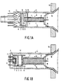
- Figs. 1a, 1b and 1c are detailed sectional views of a cathode ray tube 1 in the neck 2 of which there is provided an electron gun 3 having a system of electrodes 4, a resistive-layer lens system 5 and a cathode 6.
- the system of electrodes 4 comprises electrodes 7 and 8 which are mechanically interconnected by electrically insulating connecting rods 10 of, for example, glass.
- the resistive-layer lens system 5 comprises one or more tubular elements 11 whose inside is provided with a resistive layer 12 having a relatively high resistance.
- the resistive-layer lens system 5 shown in Fig. 1a comprises two portions and electrodes 14 and 15. The first portion forms a pre-focusing lens, the second portion forms a main lens.
- the resistive-layer lens system 5 shown in Fig. 1b forms a bipotential lens.
- the resistive-layer lens system 5 shown in Fig. 1c comprises a conducting ring 13 provided on the inside of the tubular element 11 and forms a unipotential lens.
- the end of the resistive-layer lens system facing away from the cathode is positioned in the neck 2 of the cathode ray tube 1 by means of an end portion 16 having springs. Said springs electrically contact the conducting layer 18.
- the electrode 9 is electrically connected to resistive layer 12 and forms part of the resistive-layer lens system which is adjacent to electrode 8.
- At least the resistive layer or resistive layers and the portions of the electron gun which are electrically connected to at least one resistive layer, for example end portion 16 or electrode 9 or a conducting ring at the end of the tubular element 11, etc., are regarded as parts of the resistive-layer lens system.
- the neck 2 comprises leadthroughs 17 for supplying voltages to parts of the electron gun.
- the electron beam(s) generated by the electron gun is (are) deflected across a display screen, not shown, by means of a deflection coil system 19.
- the spot, i.e. the target spot on the display screen, of an electron beam generated by said electron gun is often of an inferior quality than expected on the basis of electron-optical calculations.
- the invention is based, inter alia , on the insight that the above problem originates at least partly in a specific step in the method of manufacturing a cathode ray tube, namely in sparking.
- Sparking i.e. applying rapidly varying voltages (pulse voltages) between parts of the electron gun, permits the induction of flashovers (sparks), so that irregularities on the surface of said parts are removed and the quality of the cathode ray tube is improved.
- Said damage to the resistive-layer lens system is prevented by the method according to the invention by, for example, applying only (a) direct voltage(s) across the resistive-layer lens system during sparking.
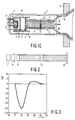
- Fig. 2 diagrammatically shows a several important parts of the electron gun shown in Fig. 1c.
- sparks may flash-over between conducting parts of said resistive-layer lens system (for example between electrode 9, conducting ring 13 or end member 16) and the high-impedance layer 12. Said sparks damage the high-impedance layer 12 and reduce the quality of the electron gun.
- the resistive-layer lens system comprises a lens system of the unipotential type.
- a voltage of approximately 30 kV is applied to both ends (electrodes 9 and 16) of the resistive-layer lens system
- a voltage of approximately 5.5 kV is applied to the centre electrode (electrode 13) of the resistive-layer lens system
- a voltage of approximately 0.5 kV is applied to an electrode (electrode 8) of the electrode system, which electrode is adjacent to the resistive-layer lens system.
- a voltage of several tens of kV for example between 25 kV and 45 kV, preferably between 30 and 40 kV, is applied to both ends (electrodes 9 and 16) of the resistive-layer lens system, which voltage, preferably, increases slowly in the course of the sparking process;
- a voltage of approximately 0 V for example between -5 kV and 5 kV, preferably ground potential, is applied to the centre electrode (electrode 13) of the resistive-layer lens system
- a negative pulse voltage of several tens of kV for example a pulse voltage between -20 kV and -30 kV, preferably approximately - 25 kV is applied to an electrode (electrode 8) of the electrode system, which electrode is adjacent to the resistive-layer lens system.
- sparks are generated between electrode 8 and a part of the resistive-layer lens system adjacent to electrode 8, in this example electrode 9.
- the resistive-layer lens system remains undamaged, and at said values there is only a small risk of flashover between the supply leads 17 during sparking.
- Table 1 lists the voltage (V9) applied to the electrodes 9 and 16, the voltage V8 applied to electrode 8 and the voltage V13 applied to electrode 13 as a function of time t (in min.).
- Fig. 3 shows an example of the voltage V8 in kV applied to electrode 8 as a function of time t (in ⁇ sec).
- the electron gun shown in Fig. 1b which comprises a resistive-layer lens system of the bipotential type can be sparked, for example, by applying a negative pulse voltage of several tens of kV to electrode 8, and by applying relatively low direct voltages, for example between 0 and 10 kV, to electrodes 9 and 16.
- the electrode system may comprise more than two electrodes; the resistive-layer lens system may comprise several sub-lens systems; the electron gun may comprise a spiral lens of the bi- and/or unipotential type; the cathode ray tube may be a monochrome cathode ray tube, for example a projection tube or a DGD-(Data Graphic Display) tube or a colour cathode ray tube of the in-line or delta type; voltages outside the ranges given in the example may be applied to the electrodes or the lens system; the electron beam(s) may be deflected by, for example, a system of deflection plates instead of the deflection coil system 19.
Landscapes
- Engineering & Computer Science (AREA)
- Manufacturing & Machinery (AREA)
- Manufacture Of Electron Tubes, Discharge Lamp Vessels, Lead-In Wires, And The Like (AREA)
Applications Claiming Priority (2)
| Application Number | Priority Date | Filing Date | Title |
|---|---|---|---|
| NL9000913A NL9000913A (nl) | 1990-04-18 | 1990-04-18 | Werkwijze voor het vervaardigen van een kathodestraalbuis. |
| NL9000913 | 1990-04-18 |
Publications (2)
| Publication Number | Publication Date |
|---|---|
| EP0454215A1 EP0454215A1 (en) | 1991-10-30 |
| EP0454215B1 true EP0454215B1 (en) | 1995-11-22 |
Family
ID=19856952
Family Applications (1)
| Application Number | Title | Priority Date | Filing Date |
|---|---|---|---|
| EP91200877A Expired - Lifetime EP0454215B1 (en) | 1990-04-18 | 1991-04-15 | Method of manufacturing a cathode ray tube |
Country Status (5)
| Country | Link |
|---|---|
| US (1) | US5127863A (ja) |
| EP (1) | EP0454215B1 (ja) |
| JP (1) | JPH04230935A (ja) |
| DE (1) | DE69114758T2 (ja) |
| NL (1) | NL9000913A (ja) |
Families Citing this family (3)
| Publication number | Priority date | Publication date | Assignee | Title |
|---|---|---|---|---|
| EP0604951B1 (en) * | 1992-12-28 | 1996-06-05 | Sony Corporation | Electron gun for a cathode ray tube |
| JPH07105867A (ja) * | 1993-08-09 | 1995-04-21 | Sony Corp | 陰極線管用電子銃 |
| US6270390B1 (en) | 1996-04-11 | 2001-08-07 | Matsushita Electric Industrial Co., Ltd. | Method for making electron gun |
Family Cites Families (7)
| Publication number | Priority date | Publication date | Assignee | Title |
|---|---|---|---|---|
| US3966287A (en) * | 1975-06-27 | 1976-06-29 | Rca Corporation | Low-voltage aging of cathode-ray tubes |
| US4326762A (en) * | 1979-04-30 | 1982-04-27 | Zenith Radio Corporation | Apparatus and method for spot-knocking television picture tube electron guns |
| JPS56168323A (en) * | 1980-05-30 | 1981-12-24 | Nec Home Electronics Ltd | Aging method for cathode-ray tube |
| US4395242A (en) * | 1981-08-19 | 1983-07-26 | Rca Corporation | Method of electrically processing a CRT mount assembly to reduce afterglow |
| US4457731A (en) * | 1982-09-28 | 1984-07-03 | U.S. Philips Corporation | Cathode ray tube processing |
| NL8600391A (nl) * | 1986-02-17 | 1987-09-16 | Philips Nv | Kathodestraalbuis en werkwijze voor het vervaardigen van een kathodestraalbuis. |
| NL8800194A (nl) * | 1988-01-27 | 1989-08-16 | Philips Nv | Kathodestraalbuis. |
-
1990
- 1990-04-18 NL NL9000913A patent/NL9000913A/nl not_active Application Discontinuation
-
1991
- 1991-04-03 US US07/679,975 patent/US5127863A/en not_active Expired - Fee Related
- 1991-04-15 DE DE69114758T patent/DE69114758T2/de not_active Expired - Fee Related
- 1991-04-15 EP EP91200877A patent/EP0454215B1/en not_active Expired - Lifetime
- 1991-04-17 JP JP3110847A patent/JPH04230935A/ja active Pending
Also Published As
| Publication number | Publication date |
|---|---|
| US5127863A (en) | 1992-07-07 |
| EP0454215A1 (en) | 1991-10-30 |
| NL9000913A (nl) | 1991-11-18 |
| DE69114758D1 (de) | 1996-01-04 |
| DE69114758T2 (de) | 1996-06-27 |
| JPH04230935A (ja) | 1992-08-19 |
Similar Documents
| Publication | Publication Date | Title |
|---|---|---|
| CA1051500A (en) | Electron gun having an extended field electrostatic focus lens | |
| US4326762A (en) | Apparatus and method for spot-knocking television picture tube electron guns | |
| US3882348A (en) | Cathode-ray tube with internal cylindrical resistor between high voltage connection and electron gun | |
| US4214798A (en) | Method for spot-knocking the electron-gun mount assembly of a CRT | |
| EP0454215B1 (en) | Method of manufacturing a cathode ray tube | |
| US5831399A (en) | Color picture tube apparatus | |
| EP0195485B1 (en) | High voltage processing of crt mounts | |
| EP0512627A2 (en) | Cathode ray tube and method of manufacturing a cathode ray tube | |
| US4531075A (en) | Electron gun having arc suppression means | |
| JPH10255682A (ja) | 陰極線管 | |
| US4491764A (en) | Arc suppression structure for an electron gun | |
| US4514661A (en) | Arc-suppression means for an electron gun having a split electrode | |
| EP0378269B1 (en) | Picture display tube | |
| US2963617A (en) | Over-voltage protective device | |
| US4305018A (en) | Electron gun structure with electrical contact spring for color television display tube | |
| US3619688A (en) | Electron gun with connector of alternate electrodes shielding intermediate electrode | |
| JPS63231847A (ja) | カラー陰極線管 | |
| US4911667A (en) | Process for reconditioning cathode ray tubes | |
| JP3023130B2 (ja) | 陰極線管の高電圧処理装置 | |
| US4600859A (en) | Cathode ray tube protection systems | |
| EP0635862B1 (en) | Cathode ray tube | |
| EP0349252A2 (en) | Method for spot-knocking an electron gun mount assembly of a CRT | |
| EP0625791A1 (en) | Dynamic convergence device for color cathode-ray tube | |
| JPS58142734A (ja) | 陰極線管のスポツトノツキング方法 | |
| KR950004851Y1 (ko) | 칼라 음극선관용 b-u 타입 전자총의 g₃ 계 방전구조 |
Legal Events
| Date | Code | Title | Description |
|---|---|---|---|
| PUAI | Public reference made under article 153(3) epc to a published international application that has entered the european phase |
Free format text: ORIGINAL CODE: 0009012 |
|
| AK | Designated contracting states |
Kind code of ref document: A1 Designated state(s): DE FR GB IT |
|
| 17P | Request for examination filed |
Effective date: 19920429 |
|
| 17Q | First examination report despatched |
Effective date: 19950118 |
|
| GRAA | (expected) grant |
Free format text: ORIGINAL CODE: 0009210 |
|
| AK | Designated contracting states |
Kind code of ref document: B1 Designated state(s): DE FR GB IT |
|
| PG25 | Lapsed in a contracting state [announced via postgrant information from national office to epo] |
Ref country code: IT Free format text: LAPSE BECAUSE OF FAILURE TO SUBMIT A TRANSLATION OF THE DESCRIPTION OR TO PAY THE FEE WITHIN THE PRE;WARNING: LAPSES OF ITALIAN PATENTS WITH EFFECTIVE DATE BEFORE 2007 MAY HAVE OCCURRED AT ANY TIME BEFORE 2007. THE CORRECT EFFECTIVE DATE MAY BE DIFFERENT FROM THE ONE RECORDED.SCRIBED TIME-LIMIT Effective date: 19951122 |
|
| REF | Corresponds to: |
Ref document number: 69114758 Country of ref document: DE Date of ref document: 19960104 |
|
| ET | Fr: translation filed | ||
| PGFP | Annual fee paid to national office [announced via postgrant information from national office to epo] |
Ref country code: GB Payment date: 19960329 Year of fee payment: 6 |
|
| PGFP | Annual fee paid to national office [announced via postgrant information from national office to epo] |
Ref country code: FR Payment date: 19960429 Year of fee payment: 6 |
|
| PLBE | No opposition filed within time limit |
Free format text: ORIGINAL CODE: 0009261 |
|
| STAA | Information on the status of an ep patent application or granted ep patent |
Free format text: STATUS: NO OPPOSITION FILED WITHIN TIME LIMIT |
|
| 26N | No opposition filed | ||
| PG25 | Lapsed in a contracting state [announced via postgrant information from national office to epo] |
Ref country code: DE Effective date: 19970101 |
|
| PG25 | Lapsed in a contracting state [announced via postgrant information from national office to epo] |
Ref country code: GB Effective date: 19970415 |
|
| GBPC | Gb: european patent ceased through non-payment of renewal fee |
Effective date: 19970415 |
|
| PG25 | Lapsed in a contracting state [announced via postgrant information from national office to epo] |
Ref country code: FR Free format text: LAPSE BECAUSE OF NON-PAYMENT OF DUE FEES Effective date: 19971231 |
|
| REG | Reference to a national code |
Ref country code: FR Ref legal event code: ST |