CN107925564B - Method and apparatus for multi-phase clock data recovery circuit calibration - Google Patents
Method and apparatus for multi-phase clock data recovery circuit calibration Download PDFInfo
- Publication number
- CN107925564B CN107925564B CN201680050195.8A CN201680050195A CN107925564B CN 107925564 B CN107925564 B CN 107925564B CN 201680050195 A CN201680050195 A CN 201680050195A CN 107925564 B CN107925564 B CN 107925564B
- Authority
- CN
- China
- Prior art keywords
- frequency
- recovery circuit
- clock recovery
- clock
- signal
- Prior art date
- Legal status (The legal status is an assumption and is not a legal conclusion. Google has not performed a legal analysis and makes no representation as to the accuracy of the status listed.)
- Active
Links
Images


Classifications
-
- H—ELECTRICITY
- H03—ELECTRONIC CIRCUITRY
- H03K—PULSE TECHNIQUE
- H03K5/00—Manipulating of pulses not covered by one of the other main groups of this subclass
- H03K5/13—Arrangements having a single output and transforming input signals into pulses delivered at desired time intervals
- H03K5/135—Arrangements having a single output and transforming input signals into pulses delivered at desired time intervals by the use of time reference signals, e.g. clock signals
-
- H—ELECTRICITY
- H04—ELECTRIC COMMUNICATION TECHNIQUE
- H04L—TRANSMISSION OF DIGITAL INFORMATION, e.g. TELEGRAPHIC COMMUNICATION
- H04L25/00—Baseband systems
- H04L25/02—Details ; arrangements for supplying electrical power along data transmission lines
- H04L25/0264—Arrangements for coupling to transmission lines
- H04L25/0272—Arrangements for coupling to multiple lines, e.g. for differential transmission
-
- H—ELECTRICITY
- H04—ELECTRIC COMMUNICATION TECHNIQUE
- H04L—TRANSMISSION OF DIGITAL INFORMATION, e.g. TELEGRAPHIC COMMUNICATION
- H04L25/00—Baseband systems
- H04L25/38—Synchronous or start-stop systems, e.g. for Baudot code
- H04L25/40—Transmitting circuits; Receiving circuits
- H04L25/49—Transmitting circuits; Receiving circuits using code conversion at the transmitter; using predistortion; using insertion of idle bits for obtaining a desired frequency spectrum; using three or more amplitude levels ; Baseband coding techniques specific to data transmission systems
- H04L25/4917—Transmitting circuits; Receiving circuits using code conversion at the transmitter; using predistortion; using insertion of idle bits for obtaining a desired frequency spectrum; using three or more amplitude levels ; Baseband coding techniques specific to data transmission systems using multilevel codes
- H04L25/4923—Transmitting circuits; Receiving circuits using code conversion at the transmitter; using predistortion; using insertion of idle bits for obtaining a desired frequency spectrum; using three or more amplitude levels ; Baseband coding techniques specific to data transmission systems using multilevel codes using ternary codes
-
- H—ELECTRICITY
- H04—ELECTRIC COMMUNICATION TECHNIQUE
- H04L—TRANSMISSION OF DIGITAL INFORMATION, e.g. TELEGRAPHIC COMMUNICATION
- H04L5/00—Arrangements affording multiple use of the transmission path
- H04L5/003—Arrangements for allocating sub-channels of the transmission path
- H04L5/0048—Allocation of pilot signals, i.e. of signals known to the receiver
-
- H—ELECTRICITY
- H04—ELECTRIC COMMUNICATION TECHNIQUE
- H04L—TRANSMISSION OF DIGITAL INFORMATION, e.g. TELEGRAPHIC COMMUNICATION
- H04L7/00—Arrangements for synchronising receiver with transmitter
- H04L7/0008—Synchronisation information channels, e.g. clock distribution lines
-
- H—ELECTRICITY
- H04—ELECTRIC COMMUNICATION TECHNIQUE
- H04L—TRANSMISSION OF DIGITAL INFORMATION, e.g. TELEGRAPHIC COMMUNICATION
- H04L7/00—Arrangements for synchronising receiver with transmitter
- H04L7/02—Speed or phase control by the received code signals, the signals containing no special synchronisation information
- H04L7/033—Speed or phase control by the received code signals, the signals containing no special synchronisation information using the transitions of the received signal to control the phase of the synchronising-signal-generating means, e.g. using a phase-locked loop
-
- H—ELECTRICITY
- H04—ELECTRIC COMMUNICATION TECHNIQUE
- H04L—TRANSMISSION OF DIGITAL INFORMATION, e.g. TELEGRAPHIC COMMUNICATION
- H04L7/00—Arrangements for synchronising receiver with transmitter
- H04L7/04—Speed or phase control by synchronisation signals
- H04L7/08—Speed or phase control by synchronisation signals the synchronisation signals recurring cyclically
-
- H—ELECTRICITY
- H04—ELECTRIC COMMUNICATION TECHNIQUE
- H04L—TRANSMISSION OF DIGITAL INFORMATION, e.g. TELEGRAPHIC COMMUNICATION
- H04L7/00—Arrangements for synchronising receiver with transmitter
- H04L7/04—Speed or phase control by synchronisation signals
Landscapes
- Engineering & Computer Science (AREA)
- Signal Processing (AREA)
- Computer Networks & Wireless Communication (AREA)
- Physics & Mathematics (AREA)
- Nonlinear Science (AREA)
- Power Engineering (AREA)
- Spectroscopy & Molecular Physics (AREA)
- Dc Digital Transmission (AREA)
- Synchronisation In Digital Transmission Systems (AREA)
- Information Transfer Systems (AREA)
- Pulse Circuits (AREA)
Abstract
Methods, apparatus, and systems for clock calibration are disclosed. A clock data recovery circuit calibration method comprises the following steps: configuring a first clock recovery circuit to provide a clock signal having a first frequency and comprising a single pulse for each symbol transmitted on a 3-wire 3-phase interface, and calibrating the first clock recovery circuit by: incrementally increasing a delay period provided by a delay element of the first clock recovery circuit until the clock signal provided by the first clock recovery circuit has a frequency less than the first frequency and, when the first clock recovery circuit has a frequency less than the first frequency, incrementally increasing the delay period provided by the delay element of the first clock recovery circuit until the clock signal provided by the first clock recovery circuit has a frequency matching the first frequency.
Description
Cross Reference to Related Applications
This application claims priority and benefit from non-provisional application No.14/842,610 filed on month 1 of 2015, U.S. patent and trademark office, the entire contents of which are incorporated herein by reference.
Technical Field
The present disclosure relates generally to high speed data communication interfaces and, more particularly, to calibration of clock generation circuits in receivers coupled to multi-wire, multi-phase data communication links.
Background
Manufacturers of mobile devices, such as cellular telephones, may obtain components of the mobile devices from a variety of sources, including different manufacturers. For example, an application processor in a cellular phone may be obtained from a first manufacturer, while an imaging device or camera may be obtained from a second manufacturer, and a display may be obtained from a third manufacturer. An application processor, imaging device, display controller, or other type of device may be interconnected using a standard-based or proprietary physical interface. In one example, the imaging device may be connected using Camera Serial Interface (CSI) as defined by the Mobile Industry Processor Interface (MIPI) alliance. In another example, the display may include an interface compliant with the Display Serial Interface (DSI) standard specified by the Mobile Industry Processor Interface (MIPI) alliance.
The multi-phase three-wire (C-PHY) interface defined by the MIPI alliance uses three conductors to transfer information between devices. During symbol transmission on the C-PHY interface, each of the three wires may be in one of three signaling states. Clock information is encoded in a sequence of symbols transmitted over the C-PHY interface, and a receiver generates a clock signal from transitions between consecutive symbols. The maximum speed of the C-PHY interface and the ability of Clock Data Recovery (CDR) circuitry to recover clock information may be limited by the maximum time variation associated with transitions of signals transmitted on different wires of the communication link. The receiver may employ delay circuitry to ensure that all three conductors have assumed a stable signaling state before providing a sampling edge. The transmission rate of the link may be limited by the delay value used and as the signalling frequency of the multi-wire interface increases, the demand for clock generation circuits that can operate reliably also increases.
SUMMARY
Embodiments disclosed herein provide systems, methods, and apparatus that enable improved communications over multi-wire and/or multi-phase communication links. The communication link may be deployed in equipment such as a mobile terminal having multiple Integrated Circuit (IC) devices.
In one aspect of the disclosure, a method of data communication includes: the first clock recovery circuit is configured to provide a clock signal having a first frequency and comprising a single pulse for each symbol transmitted on a 3-wire 3-phase interface, and to calibrate the first clock recovery circuit. The first clock recovery circuit can be calibrated by incrementally increasing the delay period provided by the delay element of the first clock recovery circuit until the clock signal provided by the first clock recovery circuit has a frequency less than the first frequency, and when the first clock recovery circuit has a frequency less than the first frequency, incrementally decreasing the delay period provided by the delay element of the first clock recovery circuit until the clock signal provided by the first clock recovery circuit has a frequency matching the first frequency.
In one aspect of the present disclosure, an apparatus for decoding data transmitted on a 3-wire 3-phase interface includes: the apparatus includes means for including a recovered signal of a first clock recovery circuit from a 3-wire 3-phase interface signal, means for configuring the first clock recovery circuit to provide a clock signal having a first frequency and including a single pulse for each symbol transmitted on the 3-wire 3-phase interface, and means for calibrating the first clock recovery circuit. The means for calibrating the first clock recovery circuit can be configured to incrementally increase the delay period provided by the delay element of the first clock recovery circuit until the clock signal provided by the first clock recovery circuit has a frequency less than the first frequency, and to incrementally decrease the delay period provided by the delay element of the first clock recovery circuit until the clock signal provided by the first clock recovery circuit has a frequency matching the first frequency when the first clock recovery circuit has a frequency less than the first frequency.
In one aspect of the disclosure, an apparatus for data communication includes: the apparatus includes a plurality of differential receivers coupled to a 3-wire bus, a clock recovery circuit configured to provide a first clock signal comprising a single pulse for each symbol transmitted in a symbol stream at a first frequency over a 3-wire 3-phase interface, and a processing circuit. The processing circuit may be configured to calibrate the first clock recovery circuit by incrementally increasing the delay period provided by the delay element of the first clock recovery circuit until the clock signal provided by the first clock recovery circuit has a frequency less than the first frequency, and when the first clock recovery circuit has a frequency less than the first frequency, incrementally decreasing the delay period provided by the delay element of the first clock recovery circuit until the clock signal provided by the first clock recovery circuit has a frequency matching the first frequency.
In one aspect of the disclosure, a processor-readable storage medium is disclosed. The storage medium may be a non-transitory storage medium and may store code that, when executed by one or more processors, causes the one or more processors to: the first clock recovery circuit is configured to provide a clock signal having a first frequency and comprising a single pulse for each symbol transmitted on a 3-wire 3-phase interface, and to calibrate the first clock recovery circuit. The first clock recovery circuit can be configured by incrementally increasing the delay period provided by the delay element of the first clock recovery circuit until the clock signal provided by the first clock recovery circuit has a frequency less than the first frequency, and when the first clock recovery circuit has a frequency less than the first frequency, incrementally decreasing the delay period provided by the delay element of the first clock recovery circuit until the clock signal provided by the first clock recovery circuit has a frequency matching the first frequency.
Brief Description of Drawings
Fig. 1 depicts an apparatus that employs a data link between IC devices that selectively operates according to one of a plurality of available standards.
Fig. 2 illustrates a system architecture of an apparatus employing data links between IC devices that selectively operate according to one of a plurality of available standards.
Fig. 3 illustrates a C-PHY 3-phase data encoder.
Fig. 4 illustrates signaling in a C-PHY 3 encoded interface.
Fig. 5 is a state diagram illustrating potential state transitions in a C-PHY 3 encoded interface.
Fig. 6 illustrates a C-PHY decoder.
Fig. 7 is an example of the effect of signal rise time on transition detection in a C-PHY decoder.
Fig. 8 illustrates transition detection in a C-PHY decoder.
Fig. 9 illustrates one example of signal transitions occurring between pairs of consecutive symbols transmitted on a C-PHY interface.
Fig. 10 illustrates transition zones and eye zones in an eye diagram.
Fig. 11 illustrates an example of an eye diagram generated for C-PHY 3 phase reception.
Fig. 12 illustrates an example of a CDR circuit for a C-PHY 3 phase interface.
Fig. 13 illustrates timing associated with the CDR circuit of fig. 12.
Fig. 14 illustrates timing associated with a CDR circuit having a loop time shorter than skew between signals transmitted on a C-PHY 3 phase signal.
Fig. 15 illustrates timing associated with a CDR circuit having a longer loop time than the symbol interval of a C-PHY 3 phase signal.
Fig. 16 is a timing diagram illustrating the operation of a CDR adapted according to certain aspects of the present disclosure.
Fig. 17 illustrates an example of a clock generation circuit in accordance with certain aspects disclosed herein.
Fig. 18 illustrates one example of a circuit that may be used to calibrate a clock generation circuit provided in accordance with certain aspects disclosed herein.
Fig. 19 is a block diagram illustrating an example of an apparatus employing processing circuitry that may be adapted according to certain aspects disclosed herein.
Fig. 20 is a flow diagram of a method of clock generation in accordance with certain aspects disclosed herein.
Fig. 21 is a diagram illustrating an example of a hardware implementation of an apparatus employing a processing circuit adapted according to certain aspects disclosed herein.
Detailed Description
The detailed description set forth below in connection with the appended drawings is intended as a description of various configurations and is not intended to represent the only configurations in which the concepts described herein may be practiced. The detailed description includes specific details to provide a thorough understanding of the various concepts. It will be apparent, however, to one skilled in the art that these concepts may be practiced without these specific details. In some instances, well-known structures and components are shown in block diagram form in order to avoid obscuring such concepts.
As used in this application, the terms "component," "module," "system," and the like are intended to include a computer-related entity, such as but not limited to hardware, firmware, a combination of hardware and software, or software in execution. For example, a component may be, but is not limited to being, a process running on a processor, an object, an executable, a thread of execution, a program, and/or a computer. By way of illustration, both an application running on a computing device and the computing device can be a component. One or more components can reside within a process and/or thread of execution and a component can be localized on one computer and/or distributed between two or more computers. In addition, these components can execute from various computer readable media having various data structures stored thereon. The components may communicate by way of local and/or remote processes such as in accordance with a signal having one or more data packets, such as data from one component interacting with another component in a local system, distributed system, and/or across a network such as the internet with other systems by way of the signal.
Furthermore, the term "or" is intended to mean an inclusive "or" rather than an exclusive "or". That is, unless specified otherwise, or clear from context, the phrase "X employs A or B" is intended to mean any of the natural inclusive permutations. That is, the phrase "X employs A or B" results in satisfaction of any of the following examples: x is A; x is B; or X employs both A and B. In addition, the articles "a," "an," and "the" as used in this application and the appended claims should generally be construed to mean "one or more" unless specified otherwise or clear from context to be directed to a singular form.
Overview
Certain aspects of the present invention may be applied to a C-PHY interface specified by the MIPI alliance that may be deployed to connect electronic devices that are subcomponents of mobile equipment such as telephones, mobile computing devices, appliances, automotive electronics, avionics systems, and the like. Examples of mobile equipment include cellular phones, smart phones, Session Initiation Protocol (SIP) phones, laptops, notebooks, netbooks, smartbooks, Personal Digital Assistants (PDAs), satellite radios, Global Positioning System (GPS) devices, multimedia devices, video devices, digital audio players (e.g., MP3 players), cameras, game consoles, wearable computing devices (e.g., smartwatches, health or fitness trackers, etc.), appliances, sensors, vending machines, or any other similar functioning device.
The C-PHY interface is a high-speed serial interface that can provide high throughput over bandwidth-limited channels. The C-PHY interface may be deployed to connect the application processor to peripheral devices (including displays and cameras). The C-PHY interface encodes data into symbols transmitted in a three-phase signal over a set of three wires, which may be referred to as a triple (trio) or triple wire. The three-phase signal is carried on each of the three conductors in a different phase. Each triplet provides a channel over the communication link. A symbol interval may be defined as a time interval in which a single symbol controls the signaling state of a triple wire. In each symbol interval, one wire is "undriven" while the remaining two of the three wires are differentially driven, such that one of the two differentially driven wires exhibits a first voltage level and the other differentially driven wire exhibits a second voltage level that is different from the first voltage level. The undriven conductor may float, be driven, and/or be terminated such that it assumes a third voltage level at or near an intermediate voltage level between the first and second voltage levels. In one example, where the undriven voltage is 0V, the driven voltage levels may be + V and-V. In another example, in the case where the undriven voltage is + V/2, the driven voltage levels may be + V and 0V. Different symbols are transmitted in each consecutively transmitted pair of symbols, and different pairs of wires may be differentially driven in different symbol intervals.
Fig. 1 depicts an example of an apparatus 100 that may employ a C-PHY 3 phase communication link. The apparatus 100 may include a wireless communication device that communicates with a Radio Access Network (RAN), a core access network, the internet, and/or another network through a Radio Frequency (RF) communication transceiver 106. The communication transceiver 106 may be operatively coupled to the processing circuitry 102. Processing circuitry 102 may include one or more IC devices, such as an application specific IC (asic) 108. ASIC 108 may include one or more processing devices, logic circuits, and the like. The processing circuit 102 may include and/or be coupled to a processor-readable storage (such as the memory device 112) that may include a processor-readable device that stores and maintains data and instructions that may be executed or otherwise used by the processing circuit 102 and a device that supports the display 124 and/or a memory card. The processing circuit 102 may be controlled by one or more of an operating system and an Application Programming Interface (API)110 layer, the API 110 layer supporting and enabling execution of software modules residing in a storage medium, such as the memory device 112 of the wireless device. Memory device 112 may include Read Only Memory (ROM), Dynamic Random Access Memory (DRAM), one or more types of Programmable Read Only Memory (PROM), flash memory cards, or any type of memory usable in processing systems and computing platforms. The processing circuitry 102 may include or access a local database 114, which local database 114 may maintain operating parameters and other information for configuring and operating the apparatus 100. The local database 114 may be implemented using one or more of a database module, flash memory, magnetic media, electrically erasable prom (eeprom), optical media, tape, floppy or hard disk, or the like. The processing circuitry may also be operatively coupled to external devices such as an antenna 122, a display 124, operator controls (such as buttons 128 and keypad 126), and other components.
Fig. 2 is a schematic block diagram illustrating certain aspects of an apparatus 200, the apparatus 200 including a plurality of IC devices 202 and 230 that may exchange data and control information over a communication link 220. The communication link 220 may be used to connect pairs of IC devices 202 and 230 located in close proximity to each other or physically located in different portions of the apparatus 200. In one example, the communication link 220 may be provided on a chip carrier, substrate, or circuit board on which the IC devices 202 and 230 are mounted. In another example, the first IC device 202 may be located in a keypad section of a fold phone and the second IC device 230 may be located in a display section of the fold phone. In another example, a portion of the communication link 220 may include a cable or an optical connection.
The IC devices 202 and 230 may each include a processor or other processing and/or computing circuitry or device 206, 236. In one example, the first IC device 202 may perform core functions of the apparatus 200, including establishing and maintaining wireless communications through the wireless transceiver 204 and the antenna 214, while the second IC device 230 may support a user interface that manages or operates the display controller 232 and may use the camera controller 234 to control operation of the camera or video input device. Other features supported by one or more of the IC devices 202 and 230 may include a keyboard, voice recognition components, and other input or output devices. The display controller 232 may include circuitry and software drivers to support a display, such as a Liquid Crystal Display (LCD) panel, touch screen display, pointer, and the like. The storage media 208 and 238 may include transitory and/or non-transitory storage devices adapted to maintain instructions and data used by the respective processors 206 and 236, and/or other components of the IC devices 202 and 230. Communication between each processor 206, 236 and its respective storage medium 208 and 238, as well as other modules and circuitry, may be facilitated by one or more internal buses 212 and 242 and/or channels 222, 223, and/or 226 of communication link 220, respectively.
The reverse channel 224 may operate in the same manner as the forward channel 222, and the forward channel 222 and the reverse channel 224 may be capable of transmitting at comparable speeds or at different speeds, where the speeds may be represented as data transmission rates and/or clock rates. The forward and reverse data rates may be substantially the same or different by several orders of magnitude, depending on the application. In some applications, a single bidirectional channel 226 may support communication between the first IC device 202 and the second IC device 230. The forward channel 222 and/or the reverse channel 224 may be configurable to operate in a bi-directional mode when, for example, the forward and reverse channels 222 and 224 share the same physical connection and operate in a half-duplex manner. In one example, the communication link 220 may be operable to communicate control, command, and other information between the first IC device 202 and the second IC device 230 in accordance with industry or other standards.
The N-phase polarity encoding devices 210 and/or 240 are generally capable of encoding multiple bits per transition on the communication link 220. In one example, a combination of 3-phase encoding and polarity encoding may be used for an LCD driver IC supporting 80 frames per second Wide Video Graphics Array (WVGA) without the need for a frame buffer, which delivers pixel data at 810Mbps for display refresh.
Fig. 3 is a schematic diagram 300 illustrating a 3-wire, 3-phase polarity encoder that may be used to implement certain aspects of the communication link 220 depicted in fig. 2. The example of 3-line, 3-phase encoding has been chosen merely for the purpose of simplifying the description of certain aspects of the present invention. The principles and techniques disclosed for a 3-wire, 3-phase encoder may be applied in other configurations of M-wire, N-phase polarity encoders.
The signaling states defined for each of the 3 wires in the 3-wire, 3-phase polarity encoding scheme may include an undriven state, a positive driven state, and a negative driven state. The positive drive state and the negative drive state may be obtained by providing a voltage differential between two of the signal conductors 310a, 310b, and/or 310c, and/or by driving current through two of the serially connected signal conductors 310a, 310b, and/or 310c such that current flows in different directions in the two signal conductors 310a, 310b, and/or 310 c. The undriven state may be achieved by placing the output of the driver of signal conductor 310a, 310b, or 310c in a high impedance mode. Alternatively or additionally, an undriven state may be obtained on a signal conductor 310a, 310b, or 310c by passively or actively causing an "undriven" signal conductor 310a, 310b, or 310c to reach a voltage level substantially midway between the positive and negative voltage levels provided on a driven signal conductor 310a, 310b, and/or 310 c. Typically, there is no significant current flow through the undriven signal conductor 310a, 310b, or 310 c. These three voltage or current states (+1, -1, and 0) can be used to indicate the signaling states defined for the 3-wire, 3-phase polarity encoding scheme.
A 3-wire, 3-phase polarity encoder may employ a wire driver 308 to control the signaling state of signal conductors 310a, 310b, and 310 c. Driver 308 may be implemented as a unit level current mode or voltage mode driver. In one example, each driver 308 may receive a set of two or more signals 316a, 316b, and 316c that determine the output state of the corresponding signal conductor 310a, 310b, and 310 c. In one example, the set of two signals 316a, 316b, and 316c may include a pull-up signal (PU signal) and a pull-down signal (PD signal) that, when high, activate pull-up and pull-down circuits that drive signal conductors 310a, 310b, and 310c toward a higher or lower level, respectively. In this example, signal conductors 310a, 310b, and 310c may be terminated at the intermediate voltage level when both the PU signal and the PD signal are low.
For each transmitted symbol interval in an M-wire, N-phase polarity encoding scheme, at least one signal conductor 310a, 310b, or 310c is in a mid-level/undriven (0) voltage or current state, while the number of positively-driven (+1 voltage or current state) signal conductors 310a, 310b, or 310c is equal to the number of negatively-driven (-1 voltage or current state) signal conductors 310a, 310b, or 310c, such that the sum of the currents flowing to the receiver is always zero. For each symbol, the state of at least one signal conductor 310a, 310b or 310c is changed with respect to the symbol transmitted in the previous transmission interval.
In operation, mapper 302 may receive 16-bit data 310 and map it to 7 symbols 312. In the 3-wire example, each of the 7 symbols defines the state of signal conductors 310a, 310b, and 310c for one symbol interval. The 7 symbols 312 may be serialized using a parallel-to-serial converter 304, the parallel-to-serial converter 304 providing a timed sequence of symbols 314 for each signal wire 310a, 310b, and 310 c. The sequence of symbols 314 is typically timed using a transmission clock. 3-wire 3-phase encoder 306 receives 7-symbol sequence 314 produced by the mapper one symbol at a time and computes the state of each signal conductor 310a, 310b, and 310c for each symbol interval. 3-wire encoder 306 selects the state of signal conductors 310a, 310b, and 310c based on the current input symbol 314 and the previous state of signal conductors 310a, 310b, and 310 c.
The use of M-line, N-phase encoding permits a number of bits to be encoded in multiple symbols, with each codeThe bits of the element are not integers. In the example of a 3-wire communication link, there are 3 available 2 wire combinations that can be driven simultaneously, and 2 possible polarity combinations on the wire pairs that are driven, resulting in 6 possible states. Since each transition occurs from the current state, 5 states out of 6 are available at each transition. At each transition, a change of state of at least one of the conductors is required. In the case of 5 states, each symbol can be encoded And (4) a bit. Accordingly, the mapper may accept the 16-bit word and convert it to 7 symbols, since 7 symbols carrying 2.32 bits per symbol may encode 16.24 bits. In other words, the combination of seven symbols encoding five states has 57(i.e., 78,125). Accordingly, the 7 symbols may be used to encode 16 bits of 216(65,536) kinds of arrangements.
Fig. 4 includes an example of a timing diagram 400 of signals encoded using a three-phase modulation data encoding scheme based on a cycle state diagram 450. Information may be encoded in a sequence of signaling states in which, for example, a wire or connector is in a three-phase state S defined by the cyclical state diagram 4501、S2And S3One of them. Each state may be separated from the other states by a 120 phase shift. In one example, data may be encoded in the direction of rotation of the phase state on the wire or connector. The phase states in the signal may rotate in either clockwise direction 452 and 452 'or counterclockwise direction 454 and 454'. For example, in clockwise directions 452 and 454', the phase states may include from S1To S2From S2To S3And from S3To S1Is advanced in sequence of one or more of the transitions of (a). In the counterclockwise directions 454 and 454', the phase state may include S1To S3From S3To S2And from S2To S1Is advanced in sequence of one or more of the transitions of (a). The three signal conductors 310a, 310b and 310c carry different versions of the same signal, wherein the versions may be phase shifted 120 ° with respect to each other. Each one of which isThe signaling state may be represented as different voltage levels on the wire or connector and/or the direction of current flow through the wire or connector. During each state in a sequence of signaling states in a 3-wire system, each signal conductor 310a, 310b, and 310c is in a different signaling state than the other conductors. When more than 3 signaling wires 310a, 310b, and 310c are used in a 3-phase encoding system, two or more signaling wires 310a, 310b, and/or 310c may be in the same signaling state in each signaling interval, but each state is present on at least one signaling wire 310a, 310b, and/or 310c in each signaling interval.
Information may be encoded in the direction of rotation at each phase transition 410, and a 3-phase signal may change direction for each signaling state. The direction of rotation may be determined by considering which signal conductors 310a, 310b and/or 310c are in a '0' state before and after the phase transition, because the undriven signal conductors 310a, 310b and/or 310c change at each signaling state in the rotating three-phase signal, regardless of the direction of rotation.
The encoding scheme may also encode information in the polarity 408 of the two signal conductors 310a, 310b, and/or 310c that are actively driven. At any time in a 3-wire implementation, exactly two of the signal conductors 310a, 310b, 310c are driven with currents in opposite directions and/or with a differential voltage. In one implementation, the data may be encoded using two bit values 412, where one bit is encoded in the direction of the phase transition 410 and the second bit is encoded in the polarity 408 of the current state.
The timing diagram 400 illustrates data encoding using both phase rotation direction and polarity. Curves 402, 404 and 406 relate to the signals carried on the three signal conductors 310a, 310b and 310c, respectively, for a plurality of phase states. Initially, the phase transition 410 is clockwise and the most significant bit is set to a binary '1' until the rotation of the phase transition 410 switches to a counter-clockwise direction at time 414 (as represented by the binary '0' of the most significant bit). The least significant bits reflect the polarity 408 of the signal in each state.
According to certain aspects disclosed hereinOne bit of data may be encoded in the rotation or phase change in a 3-wire, 3-phase encoding system, while additional bits may be encoded in the polarity of the two driven wires. Additional information may be encoded in each transition of the 3-wire, 3-phase encoding system by allowing a transition from the current state to any one of the possible states. Given 3 rotational phases and two polarities for each phase, 6 states are available in a 3-line, 3-phase encoding system. Accordingly, 5 states can be derived from any current state, and each symbol (transition) can be encoded One bit, which allows
 mapper 302 to accept the 16-bit word and encode it into 7 symbols.
N-phase data transmission may use more than three wires provided in a communication medium, such as a bus. The use of additional signal conductors that can be driven simultaneously provides more combinations of states and polarities and allows more bits of data to be encoded at each transition between states. This may significantly improve the throughput of the system and reduce power consumption relative to approaches that use multiple differential pairs to transmit data bits, while providing increased bandwidth.
In one example, an encoder may use 6 wires to transmit symbols, where for each state, 2 pairs of wires are driven. The 6 conductors may be labeled a through F such that in one state, conductors a and F are driven positive, conductors B and E are driven negative, and C and D are not driven (or carry no current). For 6 wires, there may be:

a possible combination of actively driven conductors, wherein for each phase state there is:

a different combination of polarities.
These 15 different actively driven wire combinations may include:

of the 4 driven wires, there may be a combination of two wires driven positive (while the other two must be driven negative). The polarity combinations may include:
++-- +--+ +-+- -+-+ -++- --++
accordingly, the total number of different states may be calculated as 15 × 6 ═ 90. To ensure transitions between symbols, 89 states are available from any current state, and the number of bits that can be encoded in each symbol can be calculated as: each code element And (4) a bit. In this example, given 32.35 bits of 5 × 6.47, the mapper may encode a 32-bit word into 5 symbols.
For any size bus, the general equation for the number of wire combinations that can be driven is a function of the number of wires in the bus and the number of wires that are driven simultaneously:

one equation for calculating the number of polarity combinations of the driven wires is:

the equivalent number of bits per symbol can be expressed as:

fig. 5 is a state diagram 500 illustrating 6 states and 30 possible state transitions in one example of a 3-wire, 3-phase communication link. The possible states 502, 504, 506, 512, 514, and 516 in state diagram 500 include and extend over the states shown in the looping state diagram 450 of FIG. 4. As shown in the example of state element 520, each state 502, 504, 506, 512, 514, and 516 in state diagram 502 includes a field 522 showing the voltage state of signals A, B and C (transmitted on signal conductors 310a, 310b, and 310C, respectively), a field 524 showing the result after the conductor voltage is subtracted by a differential receiver (see, e.g., differential receiver 602 of fig. 6, respectively), and a field 526 indicating the direction of rotation. For example, in state 502(+ x), conductor a is +1, conductor B is-1, and conductor C is 0, resulting in an output (a-B) ═ 2 for differential receiver 702a, an output (B-C) ═ 1 for differential receiver 702B, and an output (C-a) ═ 1 for differential receiver 702C. As illustrated by the state diagram, the transition decisions made by the phase change detection circuitry in the receiver are based on the 5 possible levels produced by each differential receiver, including the-2, -1, 0, +1, and +2 voltage states.
Fig. 6 is a diagram 600 illustrating certain aspects of a 3-wire, 3-phase decoder 600. The differential receiver 602 and the wire state decoder 604 are configured to provide digital representations of the states of the three transmission lines (e.g., the signal wires 310a, 310b, and 310c illustrated in fig. 3) relative to one another, and to detect changes in the states of the three transmission lines as compared to the state transmitted in the previous symbol period. Seven coherent states are assembled by serial-to-parallel converter 606 to obtain a set of 7 symbols to be processed by demapper 608. The demapper 608 produces 16-bit data that may be buffered in a first-in-first-out (FIFO) register 610
Jitter in 3-phase interfaces
The 3-phase transmitter includes drivers that provide high, low, and mid-level voltages onto the transmit channels. This may result in some variable transition time between consecutive symbol intervals. The high-to-low and low-to-high voltage transitions may be referred to as full-swing transitions, while the low-to-mid and high-to-mid voltage transitions may be referred to as half-swing transitions. Different types of transitions may have different rise or fall times and may result in different zero crossings at the receiver. These differences can result in "coding jitter," which can affect link signal integrity performance.
Fig. 7 is a timing diagram 700 illustrating certain aspects of transition variability at the output of a C-PHY 3 phase transmitter. Variability in signal transition times can be attributed to the presence of different voltage and/or current levels used in 3-phase signaling. Timing diagram 700 illustrates transition times of signals received from a single signal conductor 310a, 310b, or 310 c. In the second symbol Sym n+1724 first symbol Sym when transmitted in a second symbol interval n702 is transmitted in a first symbol interval ending at time 722. In the third symbol Symn+2706 transmitted in a third symbol interval, the second symbol interval may end at time 724, the third symbol Symn+2706 at the fourth symbol Symn+3708 ends when transmitted in the fourth symbol interval. A transition from the state determined by first symbol 702 to the state corresponding to second symbol 704 may be detectable after a delay 712 attributable to the time it takes for the voltage in signal conductor 310a, 310b, or 310c to reach a threshold voltage 718 and/or 720. The threshold voltage may be used to determine the state of signal conductor 310a, 310b, or 310 c. The transition from the state determined by the second symbol 704 to the state of the third symbol 706 is attributableThe delay 714 due to the time it takes for the voltage in the signal conductor 310a, 310b, or 310c to reach one of the threshold voltages 718 and/or 720 may be detectable thereafter. The transition from the state determined by the third symbol 706 to the state of the fourth symbol 708 may be detectable after a delay 716 attributable to the time it takes for the voltage in the signal conductor 310a, 310b, or 310c to reach a threshold voltage 718 and/or 720. The delays 712, 714, 716 may have different durations that may be due in part to variations in device manufacturing processes and operating conditions, which may have unequal effects on transitions between different voltage or current levels and/or different transition magnitudes associated with these 3 states. These differences may contribute to jitter and other problems in the C-PHY 3 phase receiver.
Fig. 8 includes a schematic block diagram 800 illustrating certain aspects of CDR circuitry that may be provided in a receiver in a C-PHY 3-phase interface. The set of differential receivers 802a, 802b, and 802c is configured to: a set of differential signals 810 is generated by comparing each of the three signal wires 310a, 310b, and 310c in the triplets with another of the three signal wires 310a, 310b, and 310c in the triplets. In the depicted example, a first differential receiver 802a compares the state of signal conductors 310a and 310b, a second differential receiver 802b compares the state of signal conductors 310b and 310c, and a third differential receiver 802c compares the state of signal conductors 310a and 310 c. Accordingly, transition detection circuit 804 may be configured to detect the occurrence of a phase change because the output of at least one of differential receivers 802a, 802b, and 802c changes at the end of each symbol interval.
Some transitions between transmitted symbols may be detectable by a single differential receiver 802a, 802b, or 802c, while other transitions may be detectable by two or more of the differential receivers 802a, 802b, and 802 c. In one example, the state, or relative state of the two wires, may not change after the transition, and the output of the corresponding differential receiver 802a, 802b, or 802c may also not change after the phase transition. In another example, both wires of signal wire pair 310a, 310b, and/or 310c may be in the same state in a first time interval, and both wires may be in the same second state in a second time interval, and the corresponding differential receiver 802a, 802b, or 802c may not change after a phase transition. Accordingly, the clock generation circuitry 806 may include transition detection circuitry 804 and/or other logic to monitor the output of all of the differential receivers 802a, 802b, and 802c to determine when a phase transition has occurred, which may generate a receive clock signal 808 based on the detected phase transition.
A change in signaling state for 3 wires may be detected at different times for different combinations of signal wires 310a, 310b, and/or 310 c. The timing of detection of a change in signaling state may vary depending on the type of signaling state change that has occurred. The results of such variability are illustrated in the timing diagram 850 of fig. 8. Markers 822, 824, and 826 indicate the occurrence of transitions in the differential signal 810 provided to the transition detection circuit 804. For clarity of illustration only, the markers 822, 824, and 826 are assigned different heights in the timing diagram 850, and the relative heights of the markers 822, 824, and 826 are not intended to show a particular relationship to voltage or current levels, polarities, or weighting values for clock generation or data decoding. The timing diagram 850 illustrates the effect of the timing of transitions associated with symbols transmitted in phase and polarity on the three signal wires 310a, 310b, and 310 c. In timing diagram 850, transitions between some symbols may result in variable capture windows 830a, 830b, 830c, 830d, 830e, 830f, and/or 830g (collectively symbol capture windows 830) during which symbols may be reliably captured. The number of detected state changes and their relative timing can cause jitter in clock signal 808.
The throughput of the C-PHY communication link may be affected by the duration and variability in signal transition times. For example, variability in the detection circuit may be caused by manufacturing process tolerances, variations and stability in voltage and current sources, and operating temperatures, as well as by the electrical characteristics of the signal lines 310a, 310b, and 310 c. The variability of the detection circuit may limit the channel bandwidth.
Fig. 9 includes timing diagrams 900 and 920 representing some examples of transitions from a first signaling state to a second signaling state between some consecutive symbols. The signaling state transitions illustrated in timing diagrams 900 and 920 are selected for illustrative purposes, and other transitions or combinations of transitions may occur in the MIPI alliance C-PHY interface. Timing diagrams 900 and 920 relate to examples of 3-wire, 3-phase communication links in which multiple receiver output transitions may occur at each symbol interval boundary due to differences in rise and fall times between signal levels on the three wires. Referring also to fig. 9, a first timing diagram 900 illustrates signaling states of the triplex signal conductors 310a, 310b, and 310C (A, B, and C) before and after the transition, and a second timing diagram illustrates the outputs of the differential receivers 802a, 802b, and 802C, which provide differential signals 810 representing differences between the signal conductors 310a, 310b, and 310C. In many instances, a set of differential receivers 802a, 802b, and 802c may be configured to capture transitions by comparing different combinations of the two signal wires 310a, 310b, and 310 c. In one example, these differential receivers 802a, 802b, and 802c can be configured to produce an output by determining a difference in their respective input voltages (e.g., by subtraction).
In each of the examples shown in timing diagrams 900 and 920, the initial symbol (-z)516 (see FIG. 5) transitions to a different symbol. As shown in timing diagrams 902, 904, and 906, signal A is initially in the +1 state, signal B is in the 0 state, and signal C is in the-1 state. Accordingly, differential receivers 802a, 802b initially measure a +1 difference 924 and differential receiver 802c measures a-2 difference 926, as shown in timing diagrams 922, 932, 938 with respect to the differential receiver outputs.
In a first example corresponding to timing diagrams 902, 922, a transition occurs from symbol (-z)516 to symbol (-x)512 (see FIG. 8), where signal A transitions to a-1 state, signal B transitions to a +1 state, and signal C transitions to a 0 state, with differential receiver 802a transitioning from a +1 difference 924 to a-2 difference 930, differential receiver 802B remaining at +1 differences 924, 928, and differential receiver 802C transitioning from a-2 difference 926 to a +1 difference 928.
In a second example corresponding to timing diagrams 904, 932, a transition from symbol (-z)516 to symbol (+ z)506 occurs, where signal A transitions to a-1 state, signal B remains in a 0 state, and signal C transitions to a +1 state, two differential receivers 802a and 802B transition from a +1 difference 924 to a-1 difference 936, and differential receiver 802C transitions from a-2 difference 926 to a +2 difference 934.
In a third example corresponding to timing diagrams 906, 938, a transition occurs from symbol (-z)516 to symbol (+ x)502, where signal A remains in the +1 state, signal B transitions to the-1 state, and signal C transitions to the 0 state, differential receiver 802a transitions from a +1 difference 924 to a +2 difference 940, differential receiver 802B transitions from a +1 difference 924 to a-1 difference 942, and differential receiver 802C transitions from a-2 difference 926 to a-1 difference 942.
These examples illustrate the transition of different values across 0, 1, 2, 3, 4, and 5 levels. Pre-emphasis techniques for typical differential or single-ended serial transmitters were developed for two-level transitions, and if used on MIPI alliance C-PHY 3-phase signals, may introduce certain adverse effects-in particular, pre-emphasis circuits that overdrive signals during transitions may cause overshoot during transitions that span 1 or 2 levels, and may cause false triggering in edge-sensitive circuits.
Fig. 10 illustrates an eye diagram 1000 generated as a coverage of multiple symbol intervals, the eye diagram 1000 including a single symbol interval 1002. The signal transition region 1004 represents an uncertainty time period at the boundary between two symbols where variable signal rise times prevent reliable decoding. The state information can be reliably determined in the region defined by the eye mask 1006 within the "eye opening" which represents the time period in which the symbol is stable and can be reliably received and decoded. The eye mask 1006 masks off areas where no zero crossing occurs and is used by the decoder to prevent multiple clock clocking due to the effect of subsequent zero crossings following the first signal zero crossing at the symbol interval boundary.
The concept of periodic sampling and display of signals is useful during design, adaptation, and configuration of systems using clock data recovery circuits that recreate a received data timing signal using frequency transitions that occur in the received data. A communication system based on a serializer/deserializer (SERDES) technique is an example of a system in which the eye diagram 1000 may be used as a basis for determining the ability to reliably recover data based on the eye diagram opening of the eye diagram 1000
An M-line N-phase encoding system (such as a 3-line 3-phase encoder) may encode signals having at least one transition at each signal boundary, and the receiver may use those guaranteed transitions to recover the clock. The receiver may need reliable data immediately prior to the first signal transition at the symbol boundary, and must also be able to reliably mask the occurrence of any multiple transitions associated with the same symbol boundary. Due to the fact that Multiple receiver transitions may occur due to slight differences in rise and fall times between signals carried on (e.g., the triplets of conductors) and due to slight differences in signal propagation times between combinations of received signal pairs (e.g., the a-B, B-C and C-a outputs of the
 differential receivers 802a, 802b, and 802C of fig. 6).
Fig. 11 illustrates an example of an eye diagram 1100 generated for a C-PHY 3 phase signal. Eye diagram 1100 may be generated from a coverage of multiple symbol intervals 1102. Eye diagram 1100 may be generated using fixed and/or symbol independent triggers 1130. Eye diagram 1100 includes an increased number of voltage levels 1120, 1122, 1124, 1126, 1128 that may be attributed to the multiple voltage levels measured by differential receivers 802a, 802b, 802c (see fig. 8) of the N-phase receiver circuit. In this example, eye diagram 1100 may correspond to possible transitions in a 3-wire, 3-phase encoded signal provided to differential receivers 802a, 802b, and 802 c. The three voltage levels may cause differential receivers 802a, 802b, and 802c to generate strong voltage levels 1126, 1128 and weak voltage levels 1122, 1124 for both positive and negative polarities. Typically, only one signal conductor 310a, 310b, and 310c is undriven in any symbol, and differential receivers 802a, 802b, and 802c do not produce a 0 state (here, 0 volts) as an output. The voltages associated with the strong and weak levels need not be evenly spaced about the 0 volt level. For example, weak voltage levels 1122, 1124 represent a comparison of voltages that may include voltage levels reached by undriven signal conductors 310a, 310b, and 310 c. Eye diagram 1100 may overlap the waveforms produced by differential receivers 802a, 802b, and 802c because all three pairs of signals are considered simultaneous when data is captured at the receiving device. The waveforms generated by differential receivers 802a, 802b, and 802C represent a differential signal 810, the differential signal 810 representing a comparison of three pairs of signals (A-B, B-C and C-A).
Drivers, receivers, and other devices used in C-PHY 3 phase decoders may exhibit different switching characteristics that may introduce relative delays between signals received from the three wires. Multiple receiver output transitions may be observed at each symbol interval boundary 1108 and/or 1114 due to slight differences in rise and fall times between the three signals of the triplex signal conductors 310a, 310b, and 310c and due to slight differences in signal propagation times between combinations of signal pairs received from signal conductors 310a, 310b, and 310 c. Eye diagram 1100 may capture the changes in rise and fall times as relative delays in transitions around each symbol interval boundary 1108 and 1114. The variation in rise and fall times may be due to different characteristics of the 3-phase driver. The difference in rise and fall times for any given symbol may also result in an effective shortening or lengthening of the duration of symbol interval 1102.
The signal transition region 1104 represents a time or period of uncertainty where variable signal rise times prevent reliable decoding. The state information can be reliably determined in an "eye opening" 1106, which "eye opening" 1106 represents a time period in which the symbol is stable and can be reliably received and decoded. In one example, it may be determined that the eye opening 1106 begins at the end 1112 of the signal transition region 1104 and ends at the symbol interval boundary 1114 of the symbol interval 1102. In the example depicted in fig. 11, it may be determined that the eye opening 1106 begins at the end 1112 of the signal transition region 1104 and ends at a time 1116 when the signaling state of the signal conductors 310a, 310b, 310c and/or the outputs of the three differential receivers 802a, 802b, and 802c have begun to change to reflect the next symbol.
The maximum speed of a communication link 220 configured for N-phase encoding may be limited by the duration of the signal transition region 1104 compared to the eye opening 1106 corresponding to the received signal. The minimum period of the symbol interval 1102 may be constrained by tight design margins associated with, for example, the CDR circuit 624 in the decoder 600 illustrated in fig. 6. Different signaling state transitions may be associated with different variations in signal transition times corresponding to two or more signal conductors 310a, 310b, and/or 310c, thereby causing the outputs of differential receivers 802a, 802b, and 802c in the receiving device to change at different times and/or rates for symbol interval boundary 1108, where the inputs of differential receivers 802a, 802b, and 802c begin to change at symbol boundary 1108. Differences between signal transition times may cause timing skew between signaling transitions in two or more difference signals 810. The CDR circuitry may include delay elements and other circuitry to accommodate timing skew between the difference signals 810.
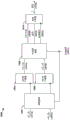
Fig. 12 provides an example of a CDR circuit 1200 for a 3-wire 3-phase interface. The illustrated CDR circuit 1200 includes certain features and functional elements that are common to many different types of clock recovery circuits. CDR circuit 1200 receives differential signals 1202, 1204, 1206, which differential signals 1202, 1204, 1206 may be derived from differential signal 810 generated by, for example, differential receivers 802a, 802b, and 802c of fig. 8. In the CDR circuit 1200, each difference signal 1202, 1204, 1206 clocks a D flip- flop pair 1210a, 1210b, 1210c to produce an output signal 1230a-1230 f. The output signals 1230a-1230f carry pulses when transitions are detected on the corresponding difference signals 1202, 1204, 1206. The rising edge of the clock input provided to the D flip-flop clocks a logic one through the D flip-flop. An inverted version of the difference signal 1202, 1204, 1206 may be provided to one of the D flip-flops in each corresponding pair of D flip-flops 1210a, 1210b, 1210c using inverters 1208a, 1208b, 1208 c. Accordingly, each D flip- flop pair 1210a, 1210b, 1210c generates a pulse in response to a rising and falling edge detected in the corresponding difference signal 1202, 1204, 1206.
For example, the AB difference signal 1202 is provided to a first D flip-flop 1232 in the first D flip-flop pair 1210a, and an inverter 1208a provides an inverted version of the AB difference signal 1202 to a second D flip-flop 1234 in the first D flip-flop pair 1210 a. The D flip-flop is initially in a reset state. The rising edge on the AB difference signal 1202 clocks a logic one through the first D flip-flop 1232, causing the output of the first flip-flop (r _ AB)1230a to transition to a logic one state. The falling edge on the AB difference signal 1202 clocks a logic one through the second D flip-flop 1234, causing the output of the second flip-flop (f _ AB)1230b to transition to a logic one state.
The output signals 1230a-1230f are provided to logic, such as an OR gate 1212, which generates an output signal that may serve as the receiver clock (RxCLK) signal 1222. The RxCLK signal 1222 transitions to a logic one state when the signaling state of any of the difference signals 1202, 1204, 1206 transitions. The RxCLK signal 1222 is provided to programmable delay element 1214, which programmable delay element 1214 drives a reset signal (rb)1228, which reset signal 1228 resets the D flip-flops in D flip- flop pair 1210a, 1210b, 1210 c. In the illustrated example, when the D flip-flop is reset by a low signal, an inverter 1216 may be included. When the D flip-flop is reset, the output of OR gate 1212 returns to a logic zero state and the pulse on RxCLK signal 1222 is terminated. When the logic zero state propagates through programmable delay element 1214 and inverter 1216, the reset condition on the D flip-flop is released. When the D flip-flop is in a reset condition, transitions on the difference signals 1202, 1204, 1206 are ignored.
The programmable delay element 1214 is generally configured to generate a delay having a duration that exceeds the difference in timing skew between the occurrences of the first and last transitions on the difference signals 1202, 1204, 1206. Programmable delay element 1214 configures the duration (i.e., pulse width) of the pulse on RxCLK signal 1222. Programmable delay element 1214 may be configured when Set (Set) signal 1226 is asserted by a processor or other control and/or configuration logic.
The RxCLK signal 1222 may also be provided to a set 1220 of three flip-flops that capture the signaling states of the difference signals 1202, 1204, 1206, thereby providing a stable output symbol 1224 for each pulse appearing on the RxCLK signal 1222. The delay or alignment logic 1218 may adjust the timing of the sets of difference signals 1202, 1204, 1206. For example, delay or alignment logic 1218 may be used to adjust the timing of the difference signals 1202, 1204, 1206 relative to pulses on the RxCLK signal 1222 to ensure that the flip-flop 1220 captures the signaling state of the difference signals 1202, 1204, 1206 when the difference signals 1202, 1204, 1206 are stable. The delay or alignment logic 1218 may delay the edges of the difference signals 1202, 1204, 1206 based on a delay configured for the programmable delay element 1214.
The programmable delay element 1214 may be configured in the CDR circuit 1200 to accommodate potentially large variations in transition times in the difference signals 1202, 1204, 1206. In one example, the programmable delay element 1214 may introduce a minimum delay period that exceeds the duration of the timing skew between the occurrence of the first and last transitions on the difference signals 1202, 1204, 1206. For reliable operation of CDR circuit 1200, the maximum delay time provided by programmable delay element 1214 may not be greater than the symbol interval. At faster data rates, the timing skew increases proportionally with the symbol interval 1102, and the eye opening 1106 may become smaller compared to the symbol interval 1102. The maximum symbol transmission rate may be limited when the timing skew reduces the percentage of symbol intervals 1102 occupied by the eye opening 1106 below a threshold size that can support reliable symbol capture.
Fig. 13 is a timing diagram illustrating certain aspects of the operation of CDR circuit 1200. This diagram relates to operation after programmable delay element 1214 has been configured and when set signal 1226 is inactive. CDR circuit 1200 operates as an edge detector. The C-PHY 3 phase encoding provides a single signaling state transition per Unit Interval (UI) 1302. Differences in the state of each of the triplets of conductive lines and/or the transmission characteristics of the triplets of conductive lines may cause transitions to occur at different times on two or more of the conductive lines. The maximum difference in the times at which transitions in difference signals 1202, 1204, 1206 occur may be referred to as the skew time (t)skew)1304. Other delays associated with CDR circuit 1200 include: through D flip-flop pair1210a, 1210b, 1210c propagation delay (t)ck2q)1314, propagation delay (t) associated with rising edge passing through OR gate 1212OR_0)1316, propagation delay (t) associated with the falling edge passing through OR gate 1212OR_1)1318, programmable delay (t) combining the delays introduced by programmable delay element 1214 and driver/inverter 1216pgm)1310, and a reset delay (t) corresponding to the delay between the time the rb signal 1228 is received by the pair of D flip-flops 1210a, 1210b, 1210c and the time the flip-flop output is clearedrst)1312。
Loop time (t)loop)1320 can be defined as:
tloop=tck2q+tOR_1+tpgm+trst+tOR_0+tpgm。
tloop1320 and UI 1302 may determine the reliability of the operation of CDR circuit 1200. This relationship is affected by the clock frequency used for transmission, which has a direct effect on the variability of the operation of the UI 1302, as well as the programmable delay element 1214.
In some devices, the operation of the programmable delay element 1214 may be affected by variations in the manufacturing process, circuit voltage supplies, and die temperature (PVT). The delay time provided by the programmable delay element 1214 for the configured value may vary significantly from device to device and/or from circuit to circuit within the device. In conventional systems, the nominal operating conditions of CDR circuit 1200 are typically designed to generate a clock edge somewhere in the middle of eye pattern opening 1106 under all PVT conditions to ensure that the clock edge still occurs after the end 1112 of signal transition region 1104 and before the beginning of the transition region to the next symbol, even under worst-case PVT effects. When the transmission frequency increases and the timing skew of the difference signals 1202, 1204, 1206 is greater compared to the UI 1302, difficulties arise in designing the CDR circuit 1200 that ensures the clock edges within the eye opening 1106. For example, a typical delay element may produce a delay value that varies by a factor of 2 under all PVT conditions.
FIG. 14 is a flowchart illustrating providing insufficient latencyTiming diagram 1400 of the effect of late programmable delay element 1214. In this example, tLoop circuit1406 for observed tDeflection1404 and generates multiple clock pulses 1408, 1410 in one UI 1402. I.e. the loop delay tLoop circuit1406 relative to tDeflection w1404 are not large enough and subsequent transitions on the difference signals 1202, 1204, 1206 are unmasked. In the depicted example, a second transition 1414 in one difference signal 1206 may be detected after generating pulse 1408 in response to a first occurring transition 1412 in the other difference signal 1202. In this example, the recovered clock frequency may be twice the clock frequency used to transmit symbols on the 3-phase interface.
Fig. 15 is a timing diagram 1500 illustrating the effect of a programmable delay element 1214 that provides too long a delay. In this example, tLoop circuit1506 is larger than the UI 1502. The CDR circuit 1200 may generate the clock pulse 1508 in response to the first occurring transition 1514 in the first UI 1502, but the rb signal 1228 may be active when transitions 1516, 1518 occur in the second UI 1512, in the depicted example, the transitions 1516, 1518 in the second UI 1512 are masked, and the expected pulse 1510 corresponding to the second UI 1512 is suppressed. In this example, the recovered clock frequency may be one half of the clock frequency used to transmit symbols on the 3-phase interface.
As illustrated by the examples of fig. 14 and 15, the CDR circuit 1200 may be subject to the following constraints:
tdeflection<tLoop circuit<UI。
Empirical evidence indicates that tLoop circuit1320. 1406, 1506 are very sensitive to PVT. In some examples, the delay provided by the programmable delay element 1214 can be increased to accommodate a range of potential variations in PVT. As the data rate increases, the duration of the UI decreases and tDeflectionThe proportional increase relative to the UI reduces the potential delay range available for configuring the programmable delay element 1214.
Clock calibration for C-PHY three-phase interface
Certain aspects disclosed herein relate to calibration of a clock recovery circuit used in a C-PHY polyphase receiver. The clock recovery circuit may be calibrated to accommodate problems associated with PVT variations. According to certain aspects, clock recovery circuitry in the C-PHY 3 receiver may be calibrated based on the UI 1302 (see fig. 13). UI 1302, which may also be referred to as a symbol transmission interval or symbol interval, is a system-defined parameter that may be assumed to remain constant in the event of PVT condition variations at the receiver.
According to certain aspects, when the cycle time tLoop circuitAnd the duration of the UI 1302 is minimized, the clock recovery circuit may be calibrated. When t isLoop circuitWhen the duration of the UI 1302 has never been exceeded, then no clock pulses are lost. When t isLoop circuitClose to the duration of the UI 1302, maximum suppression of multiple pulses in the UI 1302 is obtained. Certain aspects disclosed herein relate to a clock recovery circuit that may be used to configure a clock recovery circuit to achieve a clock signal that satisfies tLoop circuit<Limiting of UI while providing maximum jitter masked tLoop circuitA calibration procedure of duration.
Fig. 16 is a timing diagram 1600 illustrating the operation of a clock recovery circuit in a C-PHY 3 receiver that has been calibrated in accordance with certain aspects disclosed herein. In the illustrated example, tLoop circuitDuration 1604 is less than UI 1602, and tLoop circuitDuration 1604 is greater than tDeflection1612。tLoop circuitDifference between duration 1604 and UI 1602 (UI-t)Loop circuit)1606 may be minimized and potential failure modes of CDR circuit 1200 of fig. 12 may be avoided, for example, by using a calibration process to configure one or more programmable delay elements.
The calibration may include observing the frequency of the receive clock generated by the clock recovery circuit while adjusting the effect tLoop circuitOne or more delay elements of duration 1604. In the example of CDR circuit 1200 of fig. 12, programmable delay 1214 may be used to adjust tLoop circuitFor a duration 1604. The programmable delay 1214 may affect the frequency of the RxCLK signal 1222, as illustrated in the timing diagrams of fig. 14 and 15, which illustrate two potential failure modes of the CDR circuit 1200. For example, when t isCirculation of>UI time, the first of CDR circuit 1200 occursFailure mode and results in RxCLK signal 1222 recovered by CDR circuit 1200 having a frequency that is half of the nominal symbol transmission frequency of the C-PHY interface. When t isLoop circuit<tDeflectionA second failure mode of CDR circuit 1200 occurs, where tDeflectionIndicating a jitter period (compare transition 1104 of fig. 11), the RxCLK signal 1222 recovered by the CDR circuit 1200 at this time may have a frequency that is the nominal symbol transmission frequency of the C-PHY interface.
In one example, programmable delay 1214 may be initialized such that RxCLK signal 1222 has a frequency that matches the nominal symbol transmission frequency of the C-PHY interface. Programmable delay 1214 may be adjusted to increase tLoop circuitDuration 1604 until the frequency of RxCLK signal 1222 decreases, indicating that pulse generation has been inhibited for one or more transitions. Programmable delay 1214 may be set to the maximum observed to provide tLoop circuitDuration 1604 which results in RxCLK signal 1222 having a frequency that matches the nominal symbol transmission frequency of the C-PHY interface. In some examples, the value of programmable delay 1214 may be incrementally lowered until the frequency of RxCLK signal 1222 matches the transmission frequency of the C-PHY interface.
In another example, programmable delay 1214 may be initialized such that RThe xCLK signal 1222 has a frequency that is less than the nominal symbol transmission frequency of the C-PHY interface. Programmable delay 1214 may then be adjusted to reduce tLoop circuitFor a time 1604 until the frequency of the RxCLK signal 1222 matches the transmission frequency of the C-PHY interface.
According to certain aspects, the receiver does not need to know a priori the nominal symbol transmission frequency of the C-PHY interface and may determine that calibration has been completed when the training sequence is accurately received. The transmitter may send the training sequence during link initialization, before sending individual data packets, after detecting an error at the receiver, and/or under control of an application or system. The receiver may monitor the C-PHY interface for activity and may perform calibration upon detecting the transition. In some instances, the receiver may determine that CDR circuit 1200 has been calibrated and may perform calibration if the training sequence is not correctly received.
In one example, calibration begins when programmable delay 1214 is initialized to a predetermined value that enables CDR circuit 1200 to detect a training sequence. Programmable delay 1214 may then be adjusted to increase tCirculation ofFor a time 1604 until an error is detected in the training sequence. CDR circuit 1200 may be configured for normal operation where programmable delay 1214 has a value that is one or more increments lower than the value that caused the error to be detected in the training sequence.
In another example, calibration begins when programmable delay 1214 is initialized to a predetermined value, preventing CDR circuit 1200 from receiving an error-free training sequence. Programmable delay 1214 can be adjusted to increase or decrease tLoop circuitDuration 1604 until the training sequence is always error free, as received by CDR circuit 1200.
Fig. 17 is a block diagram illustrating a clock recovery circuit 1700 that may be calibrated in accordance with certain aspects disclosed herein. The clock recovery circuit 1700 may provide a first clock signal (rclk signal 1712) when the timing constrains tDeflection<tLoop circuit<UI, the first clock signal may be used to reliably capture symbols transmitted on the 3-phase interface. The clock recovery circuit 1700 includes two CDR circuits 1702, 1704 that are configuredTo generate the rclk clock signal 1712 and the second clock signal (ref _ clk signal 1714), which may be used to recover clock information from the input 1710, the input 1710 may include the difference signals 1202, 1204, 1206 and inverted versions of the difference signals 1202, 1204, 1206. The ref _ clk clock signal 1714 may be used at a frequency of FrefThe reference clock of (1). The Rclk clock signal 1712 may have a multiple of the frequency of the ref _ clk signal 1714 (i.e., 2F)ref、1Fref、0.5Fref、0.25FrefEtc.). The first CDR circuit 1702 and the second CDR circuit 1704 may have similar architectures.
The programmable delay element may be configured by adjusting the programmed delay while monitoring the frequency of the rclk clock signal 1712. Initially, the programmed delay may be initially set to a value less than the UI time (the time required to transmit one symbol). Thus, when a 3-phase signal is initially received, the clock recovery circuit may be configured to generate an rclk clock signal 1712 having a frequency equal to the symbol transmission frequency. The value of the programmed delay is then incrementally increased until the frequency of the rclk clock signal 1712 is divided by 2, 3, or by any desired factor.
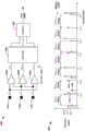
Fig. 18 illustrates one example of a CDR calibration circuit 1800 that may be used to configure delay elements of the first CDR circuit 1702. CDR calibration circuit 1800 may be enabled by signal 1812, which signal 1812 may be provided by a processing circuit. CDR calibration circuit 1800 may include conditioning logic 1802 for driving and/or adjusting the timing of ref _ clk signal 1714 and calibration clock (cal _ clk) signal 1816. In one example, the ref _ clk signal 1714 may be derived from a reference CDR circuit (e.g., the second CDR circuit 1704), a free-running oscillator, a phase-locked loop, or other clock generation circuit. CDR calibration circuit 1800 may include counters 1804 and 1806 clocked by conditioned versions of ref _ clk signal 1714 and cal _ clk signal 1816. The outputs of the counters 1804 and 1806 may be monitored by comparator logic 1808, which comparator logic 1808 may determine the frequency of the ref _ clk signal 1714 relative to the cal _ clk signal 1816. Calibration counter 1810 can be adjusted during consecutive calibration cycles to control one or more programmable delay elements in a CDR circuit (e.g., first CDR circuit 1702). Depending on the determination made by comparator logic 1808, calibration counter 1810 may be incremented or decremented, for example, after each calibration cycle. The comparator logic 1808 may control the calibration counter 1810 using one or more of an up/down signal 1818, an enable counter signal 1820, and a calibration cycle clock signal 1822.
The clock frequency may be measured using counters 1804, 1806. The counters 1804, 1814 may be incremented by the ref _ clk signal 1714 and the cal _ clk signal 1816 for a predetermined period of time, which may be determined by, for example, the calibration cycle clock signal 1824. The first counter 1804 may capture a number of clock cycles (ref _ val)1816 corresponding to the ref _ clk signal 1714. In some instances, a first counter may be operated immediately after initialization to capture ref _ val 1816 (which is a measure of the full-rate symbol transmission clock), and in some instances this initially obtained ref _ val 1816 may be registered or otherwise captured for a subsequent calibration cycle. The second counter 1806 counts the number of clock cycles (cal _ val)1818 that occur during a calibration cycle. The calibration cycle may be configured for a predetermined period of time or may be an adjustable period of time. For each calibration cycle, the control signal 1716 provides a delay parameter to the CDR circuit 1702 to be calibrated, and the frequency of the resulting cal _ clk signal 1814 may be measured as cal _ val 1818 accumulated by the second counter 1806 during the calibration cycle. When cal _ val 1818 reflects a value that is the clock frequency divided by the desired factor, the configuration is complete and the corresponding value of the delay parameter is available to operate the clock recovery circuit.
Fig. 19 is a conceptual diagram 1900 illustrating an example of a hardware implementation of an apparatus employing a processing circuit 1902 that may be configured to perform one or more of the functions disclosed herein. In accordance with various aspects of the present disclosure, an element, or any portion of an element, or any combination of elements disclosed herein may be implemented using the processing circuitry 1902. The processing circuit 1902 may include one or more processors 1904 controlled by some combination of hardware and software modules. Examples of the processor 1904 include: microprocessors, microcontrollers, Digital Signal Processors (DSPs), Field Programmable Gate Arrays (FPGAs), Programmable Logic Devices (PLDs), state machines, sequencers, gated logic, discrete hardware circuits, and other suitable hardware configured to perform the various functionalities described throughout this disclosure. The one or more processors 1904 may include a dedicated processor that performs a specific function and may be configured, augmented, or controlled by one of the software modules 1916. The one or more processors 1904 may be configured by a combination of software modules 1916 loaded during initialization, and further configured by loading or unloading one or more software modules 1916 during operation.
In the illustrated example, the processing circuit 1902 may be implemented with a bus architecture, represented generally by the bus 1910. The bus 1910 may include any number of interconnecting buses and bridges depending on the specific application of the processing circuit 1902 and the overall design constraints. The bus 1910 links together various circuits including the one or more processors 1904, and storage 1906. The storage 1906 may include memory devices and mass storage devices, and may be referred to herein as computer-readable media and/or processor-readable media. The bus 1910 may also link various other circuits such as timing sources, timers, peripherals, voltage regulators, and power management circuits. A bus interface 1908 may provide an interface between the bus 1910 and one or more transceivers 1912. The transceiver 1912 may be provided for each networking technology supported by the processing circuit. In some examples, multiple networking technologies may share some or all of the circuitry or processing modules present in the transceiver 1912. Each transceiver 1912 provides a means for communicating with various other apparatus over a transmission medium. Depending on the nature of the equipment, a user interface 1918 (e.g., keypad, display, speaker, microphone, joystick) may also be provided and the user interface 1910 may be communicatively coupled to bus 1610 directly or through bus interface 1908.
The processor 1904 may be responsible for managing the bus 1910 and general processing, including executing software stored in a computer-readable medium, which may include the storage 1906. In this regard, the processing circuitry 1902 (including the processor 1904) may be used to implement any of the methods, functions, and techniques disclosed herein. The storage 1906 may be used to store data that is manipulated by the processor 1904 when executing software, and the software may be configured to implement any of the methods disclosed herein.
One or more processors 1904 in the processing circuit 1902 may execute software. Software should be construed broadly to mean instructions, instruction sets, code segments, program code, programs, subprograms, software modules, applications, software packages, routines, subroutines, objects, executables, threads of execution, procedures, functions, algorithms, etc., whether referred to in software, firmware, middleware, microcode, hardware description language, or other terminology. The software may reside in computer-readable form in storage 1906 or in external computer-readable media. External computer-readable media and/or storage 1906 may include non-transitory computer-readable media. By way of example, a non-transitory computer-readable medium comprises: magnetic storage devices (e.g., hard disk, floppy disk, magnetic strips), optical disks (e.g., Compact Disk (CD) or Digital Versatile Disk (DVD)), smart cards, flash memory devices (e.g., "flash drive", card, stick, or key drive), Random Access Memory (RAM), ROM, PROM, erasable PROM (eprom), EEPROM, registers, removable disk, and any other suitable medium for storing software and/or instructions that may be accessed and read by a computer. By way of example, computer-readable media and/or storage 1906 may also include carrier waves, transmission lines, and any other suitable media for conveying software and/or instructions that may be accessed and read by a computer. The computer-readable medium and/or storage 1906 may reside in the processing circuit 1902, in the processor 1904, external to the processing circuit 1902, or distributed across multiple entities including the processing circuit 1902. The computer-readable medium and/or storage 1906 may be embodied in a computer program product. By way of example, a computer program product may include a computer-readable medium in packaging material. Those skilled in the art will recognize how best to implement the described functionality presented throughout this disclosure, depending on the particular application and the overall design constraints imposed on the overall system.
Some of the software modules 1916 may be loaded during initialization of the processing circuit 1902, and these software modules 1916 may configure the processing circuit 1902 to perform the various functions disclosed herein. For example, some software modules 1916 may configure internal devices and/or logic circuits 1922 of processor 1904 and may manage access to external devices (such as transceiver 1912, bus interface 1908, user interface 1918, timers, math co-processors, etc.). The software modules 1916 may include control programs and/or an operating system that interact with interrupt handlers and device drivers and control access to various resources provided by the processing circuit 1902. These resources may include memory, processing time, access to the transceiver 1912, the user interface 1918, and so forth.
One or more processors 1902 of the processing circuitry 1904 may be multi-functional, whereby some of the software modules 1916 are loaded and configured to perform different functions or different instances of the same function. The one or more processors 1904 may additionally be adapted to manage background tasks that are initiated in response to input from, for example, the user interface 1918, the transceiver 1912, and the device driver. To support the execution of multiple functions, the one or more processors 1904 may be configured to provide a multi-tasking environment whereby each function of the multiple functions is implemented as a set of tasks served by the one or more processors 1904 as needed or desired. In one example, the multitasking environment may be implemented using a time share program 1920, the time share program 1920 passing control over the processors 1904 between different tasks, whereby each task returns control of one or more processors 1904 to the time share program 1920 upon completion of any pending operations and/or in response to an input (such as an interrupt). When a task has control over one or more processors 1904, the processing circuitry is effectively dedicated to the purpose addressed by the function associated with the controller task. The timesharing program 1920 may include an operating system, a main loop that transfers control on a round-robin basis, a function that allocates control of the one or more processors 1904 according to prioritization of functions, and/or an interrupt-driven main loop that responds to external events by providing control of the one or more processors 1904 to a handle function.
Fig. 20 is a flow diagram 2000 of a method of data communication that may be performed by a receiver circuit in an apparatus coupled to a C-PHY 3 phase interface.
At block 2002, the receiver circuit may configure a first clock recovery circuit to provide a clock signal having a first frequency and comprising a single pulse for each symbol transmitted on a 3-wire 3-phase interface.
At block 2004, the receiver circuit may calibrate the first clock recovery circuit. For example, the receiver circuit may initialize the delay period of the first clock recovery circuit. The delay period may be provided by a delay element in the first clock recovery circuit.
At block 2006, the receiver circuit may incrementally increase the delay period provided by the delay element of the first clock recovery circuit until the clock signal provided by the first clock recovery circuit has a frequency less than the first frequency.
At block 2008, the receiver circuit may compare the current frequency of the clock signal to the first frequency. If the frequencies are equal, the receiver circuit may perform another calibration loop at block 2006. If the frequencies are not equal such that the first clock recovery circuit has a frequency less than the first frequency, the receiver circuit may proceed to block 2010.
At block 2010, the receiver circuit may incrementally decrease the delay period provided by the delay element of the first clock recovery circuit until the clock signal provided by the first clock recovery circuit has a frequency that matches the first frequency.
The delay element of the first clock recovery circuit may control a loop delay associated with a pulse generation cycle for generating a pulse in response to a first detected transition in a signaling state of each symbol transmitted on the 3-wire 3-phase interface. The detection of other transitions of the signaling state may be suppressed during the pulse generation cycle.
In some instances, incrementally increasing the delay period includes increasing the delay period until the clock signal provided by the first clock recovery circuit has a frequency that is one-half of the first frequency.
In some examples, the second clock recovery circuit is configured to provide a reference signal for calibrating the first clock recovery circuit. The reference signal may have a frequency that matches or corresponds to the first frequency. The second clock recovery circuit may provide the reference signal by generating a single pulse for each symbol in the stream of symbols received from the 3-wire 3-phase interface. Calibrating the first clock recovery circuit may include: the method includes comparing frequencies of a clock signal and a reference signal during each of a plurality of calibration cycles, increasing a delay period when the clock signal has a frequency greater than a frequency of the reference signal, decreasing the delay period when the clock signal has a frequency less than the frequency of the reference signal, and terminating the plurality of calibration cycles when the clock signal has a frequency equal to the frequency of the reference signal.
Calibrating the first clock recovery circuit may include configuring a delay element to provide an initial delay period. In one example, the delay period may be increased over multiple calibration cycles until the symbols received from the 3-wire 3-phase interface successfully decode the training sequence. In another example, the delay period may be decreased over multiple calibration cycles until the symbols received from the 3-wire 3-phase interface successfully decode the training sequence.
Fig. 21 is a diagram illustrating an example of a hardware implementation of the apparatus 2100 employing the processing circuit 2102. The processing circuit typically has a processor 2116, which processor 2116 may include one or more of a microprocessor, a microcontroller, a digital signal processor, a sequencer, and a state machine. The processing circuit 2102 may be implemented with a bus architecture, represented generally by the bus 2120. The bus 2120 may include any number of interconnecting buses and bridges depending on the specific application of the processing circuit 2102 and the overall design constraints. The bus 2120 links together various circuits including one or more processors and/or hardware modules (represented by the processor 2116, the modules or circuits 2104, 2106, 2108, and 2110, the differential receiver circuit 2112 that determines differential signaling states between different pairs of connectors or wires 2114, and the computer-readable storage medium 2118). The bus 2120 may also link various other circuits such as timing sources, peripherals, voltage regulators, and power management circuits, which are well known in the art, and therefore, will not be described any further.
The processor 2116 is responsible for general processing, including the execution of software stored on the computer-readable storage medium 2118. The software, when executed by the processor 2116, causes the processing circuit 2102 to perform the various functions described above for any particular apparatus. The computer-readable storage medium 2118 may also be used for storing data that is manipulated by the processor 2116 when executing software, including data decoded from symbols transmitted over a connector or conductor 2114, the connector or conductor 2114 may be configured as a data channel and a clock channel. The processing circuit 2102 further includes at least one of the modules 2104, 2106, 2108, and 2110. The modules 2104, 2106, 2108, and 2110 may be software modules that run in the processor 2116, resident/stored in the computer readable storage medium 2118, one or more hardware modules coupled to the processor 2116, or some combination thereof. The modules 2104, 2106, 2108, and/or 2110 may include microcontroller instructions, state machine configuration parameters, or some combination thereof.
In one configuration, the apparatus 2100 may be configured for data communication over a C-PHY 3 interface. The apparatus 2100 may comprise: a module and/or circuit 2104 configured to recover a clock signal from timing information embedded in a sequence of symbols transmitted over a connector or wire 2114, a module and/or circuit 2106 for generating a reference signal, and a module and/or circuit 2108 that may calibrate the clock recovery module and/or circuit 2104.
The apparatus 2100 may be configured for various modes of operation. In one example, the clock recovery module and/or circuitry 2104 may be adapted to provide a first clock signal including pulses for each symbol transmitted at a first frequency over a 3-wire 3-phase interface, the calibration module and/or circuitry 2110 may be adapted to calibrate a loop delay of the clock recovery circuitry, the clock generation module and/or circuitry 2106 may be adapted to provide a second clock signal, and the symbol capture module and/or circuitry 2108 may be adapted to capture symbols from the 3-wire 3-phase interface using the first and second clock signals. In one mode of operation, the calibration module and/or circuit 2110 modifies the first clock signal to have a second frequency that is no more than half the first frequency. In a first mode of operation, the clock recovery module and/or circuit 2104 generates pulses in the first clock signal within a first symbol of the integer number of symbols and suppresses pulse generation within other symbols of the integer number of symbols. The second clock signal may include pulses corresponding to each of the other ones of the integer number of symbols.
In some examples, the loop delay corresponds to a pulse generation cycle for generating a pulse in response to a first detected change in a signaling state of the 3-wire 3-phase interface. The detection of other transitions in the signaling state of the 3-wire 3-phase interface may be suppressed during the pulse generation cycle. The calibration module and/or circuit 2110 may be configured to program the programmable delay circuit.
In one example, the first frequency is twice the second frequency and the second clock signal includes one pulse for each pulse in the first clock signal. The second clock signal may be phase shifted by 180 degrees relative to the first clock signal. In another example, the second frequency is one third of the first frequency and the second clock signal includes two pulses for each pulse in the first clock signal. In another example, the second frequency is one-fourth of the first frequency and the second clock signal includes three pulses for each pulse in the first clock signal.
In some examples, the calibration module and/or circuitry 2110 is adapted to: causing a first circuit to recover a reference clock signal from a stream of symbols received from a 3-wire 3-phase interface, determining a current frequency of the first clock signal by comparing the frequency of the first clock signal with the reference clock signal during each of a plurality of calibration cycles, increasing a loop delay when the current frequency is determined to be greater than a second frequency, decreasing the loop delay when the current frequency is determined to be less than the second frequency, and terminating the plurality of calibration cycles when the current frequency is determined to be equal to the second frequency. The reference clock signal may have a frequency corresponding to a transmission rate of the symbol stream.
It is to be understood that the specific order or hierarchy of steps in the processes disclosed is an illustration of exemplary approaches. It should be understood that the specific order or hierarchy of steps in the processes may be rearranged based on design preferences. In addition, some steps may be combined or omitted. The accompanying method claims present elements of the various steps in a sample order, and are not meant to be limited to the specific order or hierarchy presented.
The previous description is provided to enable any person skilled in the art to practice the various aspects described herein. Various modifications to these aspects will be readily apparent to those skilled in the art, and the generic principles defined herein may be applied to other aspects. Thus, the claims are not intended to be limited to the aspects shown herein, but is to be accorded the full scope consistent with the language claims, wherein reference to an element in the singular is not intended to mean "one and only one" unless specifically so stated, but rather "one or more. The term "some" means one or more unless specifically stated otherwise. All structural and functional equivalents to the elements of the various aspects described throughout this disclosure that are known or later come to be known to those of ordinary skill in the art are expressly incorporated herein by reference and are intended to be encompassed by the claims. Moreover, nothing disclosed herein is intended to be dedicated to the public regardless of whether such disclosure is explicitly recited in the claims. No claim element should be construed as a means-plus-function unless the element is explicitly recited as using the phrase "means for … …".
Claims (30)
1. A method for data communication, comprising:
configuring a first clock recovery circuit to provide a clock signal having a first frequency and comprising a single pulse for each symbol transmitted on a 3-wire 3-phase interface; and
calibrating the first clock recovery circuit by:
incrementally increasing a delay period provided by a delay element of the first clock recovery circuit until the clock signal provided by the first clock recovery circuit has a frequency less than the first frequency; and
incrementally decreasing the delay period provided by the delay element of the first clock recovery circuit when the first clock recovery circuit has a frequency less than the first frequency until the clock signal provided by the first clock recovery circuit has a frequency matching the first frequency.
2. The method of claim 1, wherein the delay element of the first clock recovery circuit controls a loop delay associated with a pulse generation cycle used to control the loop delay associated with the pulse generation cycle used to generate a pulse in response to a first detected transition in signaling state of each symbol transmitted on the 3-wire 3-phase interface, wherein detection of other transitions in signaling state is suppressed during the pulse generation cycle.
3. The method of claim 1, wherein incrementally increasing the delay period comprises:
increasing the delay period until the clock signal provided by the first clock recovery circuit has a frequency that is half the first frequency.
4. The method of claim 1, further comprising:
configuring a second clock recovery circuit to provide a reference signal for calibrating the first clock recovery circuit, wherein the reference signal has a frequency that matches the first frequency.
5. The method of claim 4, wherein the second clock recovery circuit provides the reference signal by generating a single pulse for each symbol in the stream of symbols received from the 3-wire 3-phase interface.
6. The method of claim 4, wherein calibrating the first clock recovery circuit comprises:
comparing the frequencies of the clock signal and the reference signal during each of a plurality of calibration cycles;
increasing the delay period when the clock signal has a frequency greater than the frequency of the reference signal;
decreasing the delay period when the clock signal has a frequency less than the frequency of the reference signal; and
terminating the plurality of calibration cycles when the clock signal has a frequency equal to the frequency of the reference signal.
7. The method of claim 1, wherein calibrating the first clock recovery circuit comprises:
configuring the delay element to provide an initial delay period; and
the delay period is increased over a plurality of calibration cycles until the symbols received from the 3-wire 3-phase interface successfully decode the training sequence.
8. The method of claim 1, wherein calibrating the first clock recovery circuit comprises:
configuring the delay element to provide an initial delay period; and
the delay period is reduced over a plurality of calibration cycles until the symbols received from the 3-wire 3-phase interface successfully decode the training sequence.
9. An apparatus for data communication, comprising:
an apparatus for recovering a signal from a 3-wire 3-phase interface signal includes a first clock recovery circuit;
means for configuring the first clock recovery circuit to provide a clock signal having a first frequency and comprising a single pulse for each symbol transmitted on a 3-wire 3-phase interface; and
means for calibrating the first clock recovery circuit, the means configured to:
incrementally increasing a delay period provided by a delay element of the first clock recovery circuit until the clock signal provided by the first clock recovery circuit has a frequency less than a first frequency; and
when the first clock recovery circuit has a frequency less than the first frequency, incrementally decreasing the delay period provided by the delay element of the first clock recovery circuit until the clock signal provided by the first clock recovery circuit has a frequency matching the first frequency.
10. The apparatus of claim 9, wherein the delay element of the first clock recovery circuit controls a loop delay associated with a pulse generation cycle for controlling the loop delay associated with the pulse generation cycle for generating a pulse in response to a first detected transition in signaling state of each symbol transmitted on the 3-wire 3-phase interface, wherein detection of other transitions in signaling state is suppressed during the pulse generation cycle.
11. The apparatus of claim 9, wherein the means for calibrating the first clock recovery circuit is configured to:
incrementally increasing the delay period until the clock signal provided by the first clock recovery circuit has a frequency that is one-half of the first frequency.
12. The apparatus of claim 9, wherein the means for recovering a signal from a 3-wire 3-phase interface signal comprises a second clock recovery circuit, and further comprising:
means for configuring the second clock recovery circuit to provide a reference signal for calibrating the first clock recovery circuit, wherein the reference signal has a frequency that matches the first frequency.
13. The device of claim 12, wherein the second clock recovery circuit is configured to provide the reference signal by generating a single pulse for each symbol in a stream of symbols received from the 3-wire 3-phase interface.
14. The apparatus of claim 12, wherein the means for calibrating the first clock recovery circuit is configured to:
comparing the frequencies of the clock signal and the reference signal during each of a plurality of calibration cycles;
increasing the delay period when the clock signal has a frequency greater than the frequency of the reference signal;
decreasing the delay period when the clock signal has a frequency less than the frequency of the reference signal; and
terminating the plurality of calibration cycles when the clock signal has a frequency equal to the frequency of the reference signal.
15. The apparatus of claim 9, wherein the means for calibrating the first clock recovery circuit is configured to:
configuring the delay element to provide an initial delay period; and
the delay period is increased over a plurality of calibration cycles until the symbols received from the 3-wire 3-phase interface successfully decode the training sequence.
16. The apparatus of claim 9, wherein the means for calibrating the first clock recovery circuit is configured to:
configuring the delay element to provide an initial delay period; and
the delay period is reduced over a plurality of calibration cycles until the symbols received from the 3-wire 3-phase interface successfully decode the training sequence.
17. An apparatus for data communication, comprising:
a plurality of differential receivers coupled to the 3-wire bus;
a first clock recovery circuit configured to provide a clock signal comprising pulses corresponding to symbols transmitted in a symbol stream on a 3-wire 3-phase interface at a first frequency; and
a processing circuit configured to calibrate the first clock recovery circuit by:
incrementally increasing a delay period provided by a delay element of the first clock recovery circuit until the clock signal provided by the first clock recovery circuit has a frequency less than the first frequency; and
when the first clock recovery circuit has a frequency less than the first frequency, incrementally decreasing the delay period provided by the delay element of the first clock recovery circuit until the clock signal provided by the first clock recovery circuit has a frequency matching the first frequency.
18. The apparatus of claim 17, wherein the delay element of the first clock recovery circuit controls a loop delay associated with a pulse generation cycle for controlling the loop delay associated with the pulse generation cycle for generating a pulse in response to a first detected transition in signaling state of each symbol transmitted on the 3-wire 3-phase interface, wherein detection of other transitions in signaling state is suppressed during the pulse generation cycle.
19. The apparatus of claim 17, wherein the processing circuit is configured to calibrate the first clock recovery circuit by:
increasing the delay period until the clock signal provided by the first clock recovery circuit has a frequency that is half the first frequency.
20. The apparatus of claim 17, further comprising:
a second clock recovery circuit configured to provide a reference signal at the first frequency, wherein the reference signal is used to calibrate the first clock recovery circuit.
21. The apparatus of claim 20, wherein the second clock recovery circuit is configured to provide the reference signal by generating a single pulse for each symbol in a stream of symbols received from the 3-wire 3-phase interface.
22. The apparatus of claim 20, wherein the processing circuit is configured to calibrate the first clock recovery circuit by:
comparing the frequencies of the clock signal and the reference signal during each of a plurality of calibration cycles;
increasing the delay period when the clock signal has a frequency greater than the frequency of the reference signal;
decreasing the delay period when the clock signal has a frequency less than the frequency of the reference signal; and
terminating the plurality of calibration cycles when the clock signal has a frequency equal to the frequency of the reference signal.
23. The apparatus of claim 20, the processing circuit configured to calibrate the first clock recovery circuit by:
configuring the delay element to provide an initial delay period; and
the delay period is increased over a plurality of calibration cycles until the symbols received from the 3-wire 3-phase interface successfully decode the training sequence.
24. The apparatus of claim 20, the processing circuit configured to calibrate the first clock recovery circuit by:
configuring the delay element to provide an initial delay period; and
the delay period is reduced over a plurality of calibration cycles until the symbols received from the 3-wire 3-phase interface successfully decode the training sequence.
25. A processor-readable storage medium comprising code for:
configuring a first clock recovery circuit to provide a clock signal having a first frequency and comprising a single pulse for each symbol transmitted on a 3-wire 3-phase interface; and
calibrating the first clock recovery circuit by:
incrementally increasing a delay period provided by a delay element of the first clock recovery circuit until the clock signal provided by the first clock recovery circuit has a frequency less than the first frequency; and
when the first clock recovery circuit has a frequency less than the first frequency, incrementally decreasing the delay period provided by the delay element of the first clock recovery circuit until the clock signal provided by the first clock recovery circuit has a frequency matching the first frequency.
26. The storage medium of claim 25, wherein the delay element of the first clock recovery circuit controls a loop delay associated with a pulse generation cycle used to control the loop delay associated with the pulse generation cycle used to generate pulses in response to a first detected transition in signaling state of each symbol transmitted on the 3-wire 3-phase interface, wherein detection of other transitions in signaling state is suppressed during the pulse generation cycle.
27. The storage medium of claim 25, wherein incrementally increasing the delay period comprises:
increasing the delay period until the clock signal provided by the first clock recovery circuit has a frequency that is half the first frequency.
28. The storage medium of claim 25, further comprising:
configuring a second clock recovery circuit to provide a reference signal for calibrating the first clock recovery circuit, wherein the reference signal has a frequency that matches the first frequency.
29. The storage medium of claim 28, wherein calibrating the first clock recovery circuit comprises:
comparing the frequencies of the clock signal and the reference signal during each of a plurality of calibration cycles;
increasing the delay period when the clock signal has a frequency greater than the frequency of the reference signal;
decreasing the delay period when the clock signal has a frequency less than the frequency of the reference signal; and
terminating the plurality of calibration cycles when the clock signal has a frequency equal to the frequency of the reference signal.
30. The storage medium of claim 25, wherein calibrating the first clock recovery circuit comprises:
configuring the delay element to provide an initial delay period; and
the delay period is adjusted over a plurality of calibration cycles until the symbols received from the 3-wire 3-phase interface successfully decode the training sequence.
Priority Applications (1)
| Application Number | Priority Date | Filing Date | Title |
|---|---|---|---|
| CN202011577819.6A CN112751660B (en) | 2015-09-01 | 2016-08-09 | Method and apparatus for multiphase clock data recovery circuit calibration |
Applications Claiming Priority (3)
| Application Number | Priority Date | Filing Date | Title |
|---|---|---|---|
| US14/842,610 | 2015-09-01 | ||
| US14/842,610 US9485080B1 (en) | 2015-09-01 | 2015-09-01 | Multiphase clock data recovery circuit calibration |
| PCT/US2016/046208 WO2017039984A1 (en) | 2015-09-01 | 2016-08-09 | Multiphase clock data recovery circuit calibration |
Related Child Applications (1)
| Application Number | Title | Priority Date | Filing Date |
|---|---|---|---|
| CN202011577819.6A Division CN112751660B (en) | 2015-09-01 | 2016-08-09 | Method and apparatus for multiphase clock data recovery circuit calibration |
Publications (2)
| Publication Number | Publication Date |
|---|---|
| CN107925564A CN107925564A (en) | 2018-04-17 |
| CN107925564B true CN107925564B (en) | 2020-12-29 |
Family
ID=56694263
Family Applications (2)
| Application Number | Title | Priority Date | Filing Date |
|---|---|---|---|
| CN201680050195.8A Active CN107925564B (en) | 2015-09-01 | 2016-08-09 | Method and apparatus for multi-phase clock data recovery circuit calibration |
| CN202011577819.6A Active CN112751660B (en) | 2015-09-01 | 2016-08-09 | Method and apparatus for multiphase clock data recovery circuit calibration |
Family Applications After (1)
| Application Number | Title | Priority Date | Filing Date |
|---|---|---|---|
| CN202011577819.6A Active CN112751660B (en) | 2015-09-01 | 2016-08-09 | Method and apparatus for multiphase clock data recovery circuit calibration |
Country Status (11)
| Country | Link |
|---|---|
| US (1) | US9485080B1 (en) |
| EP (2) | EP3345333B1 (en) |
| JP (2) | JP7027307B2 (en) |
| KR (1) | KR102523235B1 (en) |
| CN (2) | CN107925564B (en) |
| BR (1) | BR112018004151B1 (en) |
| CA (1) | CA2992750A1 (en) |
| ES (1) | ES2794527T3 (en) |
| HU (1) | HUE049096T2 (en) |
| TW (1) | TWI699974B (en) |
| WO (1) | WO2017039984A1 (en) |
Families Citing this family (27)
| Publication number | Priority date | Publication date | Assignee | Title |
|---|---|---|---|---|
| US10289600B2 (en) | 2013-08-08 | 2019-05-14 | Qualcomm Incorporated | Reducing transmitter encoding jitter in a C-PHY interface using multiple clock phases to launch symbols |
| US9276731B2 (en) * | 2013-08-08 | 2016-03-01 | Qualcomm Incorporated | N-phase signal transition alignment |
| TWI587663B (en) * | 2016-01-25 | 2017-06-11 | 國立交通大學 | Bpsk demodulator |
| US10742390B2 (en) * | 2016-07-13 | 2020-08-11 | Novatek Microelectronics Corp. | Method of improving clock recovery and related device |
| US10419246B2 (en) * | 2016-08-31 | 2019-09-17 | Qualcomm Incorporated | C-PHY training pattern for adaptive equalization, adaptive edge tracking and delay calibration |
| US10033519B2 (en) * | 2016-11-10 | 2018-07-24 | Qualcomm Incorporated | C-PHY half-rate clock and data recovery adaptive edge tracking |
| US10284361B2 (en) | 2017-05-05 | 2019-05-07 | Mediatek Inc. | Channel skew calibration method and associated receiver and system |
| US10298381B1 (en) * | 2018-04-30 | 2019-05-21 | Qualcomm Incorporated | Multiphase clock data recovery with adaptive tracking for a multi-wire, multi-phase interface |
| US10333690B1 (en) | 2018-05-04 | 2019-06-25 | Qualcomm Incorporated | Calibration pattern and duty-cycle distortion correction for clock data recovery in a multi-wire, multi-phase interface |
| CN108900181B (en) * | 2018-07-02 | 2022-07-29 | 天津芯海创科技有限公司 | Clock delay adjusting device and clock delay adjusting system |
| US10382190B1 (en) | 2018-07-13 | 2019-08-13 | Qualcomm Incorporated | Optimizing clock/data recovery power while maintaining link stability in source synchronous applications |
| TWI681635B (en) * | 2018-11-21 | 2020-01-01 | 國立交通大學 | System of referenceless clock and data recovery and frequency detector thereof |
| CN110134177A (en) * | 2018-11-30 | 2019-08-16 | 中电普瑞科技有限公司 | A kind of embedded system timing system and its method applied to smart grid |
| US10581587B1 (en) * | 2019-04-29 | 2020-03-03 | Advanced Micro Devices, Inc. | Deskewing method for a physical layer interface on a multi-chip module |
| US11108604B2 (en) * | 2019-08-19 | 2021-08-31 | Qualcomm Incorporated | Driver architecture for multiphase and amplitude encoding transmitters |
| US11095425B2 (en) * | 2019-10-25 | 2021-08-17 | Qualcomm Incorporated | Small loop delay clock and data recovery block for high-speed next generation C-PHY |
| US11240077B2 (en) * | 2019-10-29 | 2022-02-01 | Qualcomm Incorporated | C-PHY half-rate wire state encoder and decoder |
| US11038666B1 (en) * | 2019-12-11 | 2021-06-15 | Qualcomm Incorporated | Open-loop, super fast, half-rate clock and data recovery for next generation C-PHY interfaces |
| US11327914B1 (en) * | 2021-01-29 | 2022-05-10 | Qualcomm Incorporated | C-PHY data-triggered edge generation with intrinsic half-rate operation |
| CN113114190B (en) * | 2021-04-08 | 2024-02-06 | 格科微电子(上海)有限公司 | Clock recovery circuit and method, data processing chip and electronic equipment |
| JP2023023090A (en) * | 2021-08-04 | 2023-02-16 | 株式会社アドバンテスト | Device |
| TWI769046B (en) * | 2021-08-10 | 2022-06-21 | 瑞昱半導體股份有限公司 | Signal relay apparatus and method having frequency calibration mechanism |
| CN113886315B (en) * | 2021-09-23 | 2024-05-03 | 珠海一微半导体股份有限公司 | Clock data recovery system, chip and clock data recovery method |
| CN113886300B (en) * | 2021-09-23 | 2024-05-03 | 珠海一微半导体股份有限公司 | Clock data self-adaptive recovery system and chip of bus interface |
| CN115903998A (en) * | 2022-11-11 | 2023-04-04 | 深圳天德钰科技股份有限公司 | Calibration method, calibration circuit, storage medium, clock recovery circuit, and electronic device |
| CN116825170B (en) * | 2023-08-31 | 2023-11-07 | 芯砺智能科技(上海)有限公司 | Automatic calibration architecture and chip for die-to-die interconnect |
| CN117056269B (en) * | 2023-10-11 | 2024-02-09 | 芯耀辉科技有限公司 | Data alignment method for parallel interface connection, computer equipment and medium |
Citations (5)
| Publication number | Priority date | Publication date | Assignee | Title |
|---|---|---|---|---|
| CN1574629A (en) * | 2003-06-11 | 2005-02-02 | 恩益禧电子股份有限公司 | Clock and data recovery circuit |
| CN1780488A (en) * | 2004-11-23 | 2006-05-31 | 中兴通讯股份有限公司 | Clock calibrater and calibration for program control switchboard system |
| CN102456087A (en) * | 2010-11-03 | 2012-05-16 | 上海华虹集成电路有限责任公司 | Method for repairing establishing timing sequence |
| CN103684363A (en) * | 2012-09-12 | 2014-03-26 | 辉达公司 | Timing calibration for on-chip interconnec |
| CN104113329A (en) * | 2013-04-18 | 2014-10-22 | 瑞萨电子株式会社 | Frequency-locked loop circuit and semiconductor integrated circuit |
Family Cites Families (23)
| Publication number | Priority date | Publication date | Assignee | Title |
|---|---|---|---|---|
| US5771264A (en) * | 1996-08-29 | 1998-06-23 | Altera Corporation | Digital delay lock loop for clock signal frequency multiplication |
| US6236697B1 (en) * | 1998-05-28 | 2001-05-22 | Integrated Device Technology, Inc. | Clock recovery for multiple frequency input data |
| US6889334B1 (en) | 2001-10-02 | 2005-05-03 | Advanced Micro Devices, Inc. | Multimode system for calibrating a data strobe delay for a memory read operation |
| DE10202879B4 (en) * | 2002-01-25 | 2004-01-29 | Infineon Technologies Ag | DLL (Delay-Locked-Loop) circuit |
| JP2006520169A (en) | 2003-03-04 | 2006-08-31 | タイムラブ コーポレーション | Clock and data recovery method and circuit |
| US7436919B2 (en) * | 2005-04-01 | 2008-10-14 | Freescale Semiconductor, Inc. | Methods and apparatus for bit synchronizing data transferred across a multi-pin asynchronous serial interface |
| US7685216B2 (en) * | 2005-07-07 | 2010-03-23 | Texas Instruments Incorporated | Automatic input error recovery circuit and method for recursive digital filters |
| JP4795032B2 (en) | 2006-01-30 | 2011-10-19 | エルピーダメモリ株式会社 | Timing adjustment circuit and semiconductor device |
| KR100782791B1 (en) * | 2006-08-31 | 2007-12-05 | 삼성전기주식회사 | Digital modulation circuit |
| US7940667B1 (en) | 2006-09-13 | 2011-05-10 | Pmc-Sierra Us, Inc. | Delay measurements and calibration methods and apparatus for distributed wireless systems |
| JP2008206101A (en) | 2007-02-22 | 2008-09-04 | Nec Corp | Data transmission/reception system, and transmission circuit and reception circuit for use therein |
| US9711041B2 (en) * | 2012-03-16 | 2017-07-18 | Qualcomm Incorporated | N-phase polarity data transfer |
| JP4404122B2 (en) | 2007-09-07 | 2010-01-27 | セイコーエプソン株式会社 | High-speed serial interface circuit and electronic equipment |
| US7622969B2 (en) * | 2007-12-18 | 2009-11-24 | Micron Technology, Inc. | Methods, devices, and systems for a delay locked loop having a frequency divided feedback clock |
| US7826279B2 (en) | 2008-04-10 | 2010-11-02 | Advanced Micro Devices, Inc. | Programmable bias circuit architecture for a digital data/clock receiver |
| US7642827B2 (en) * | 2008-05-28 | 2010-01-05 | Micron Technology, Inc. | Apparatus and method for multi-phase clock generation |
| US20130216003A1 (en) * | 2012-02-16 | 2013-08-22 | Qualcomm Incorporated | RESETTABLE VOLTAGE CONTROLLED OSCILLATORS (VCOs) FOR CLOCK AND DATA RECOVERY (CDR) CIRCUITS, AND RELATED SYSTEMS AND METHODS |
| JP6027359B2 (en) | 2012-07-24 | 2016-11-16 | ラピスセミコンダクタ株式会社 | Clock data recovery circuit and semiconductor device |
| JP2014123796A (en) * | 2012-12-20 | 2014-07-03 | Sony Corp | Clock and data recovery circuit, data reception device and data transmission and reception system |
| US9178690B2 (en) * | 2013-10-03 | 2015-11-03 | Qualcomm Incorporated | N factorial dual data rate clock and data recovery |
| US9137008B2 (en) | 2013-07-23 | 2015-09-15 | Qualcomm Incorporated | Three phase clock recovery delay calibration |
| US9276731B2 (en) * | 2013-08-08 | 2016-03-01 | Qualcomm Incorporated | N-phase signal transition alignment |
| US9496879B1 (en) * | 2015-09-01 | 2016-11-15 | Qualcomm Incorporated | Multiphase clock data recovery for a 3-phase interface |
-
2015
- 2015-09-01 US US14/842,610 patent/US9485080B1/en active Active
-
2016
- 2016-08-09 JP JP2018510818A patent/JP7027307B2/en active Active
- 2016-08-09 WO PCT/US2016/046208 patent/WO2017039984A1/en unknown
- 2016-08-09 EP EP16753547.5A patent/EP3345333B1/en active Active
- 2016-08-09 KR KR1020187009212A patent/KR102523235B1/en active IP Right Grant
- 2016-08-09 CN CN201680050195.8A patent/CN107925564B/en active Active
- 2016-08-09 BR BR112018004151-3A patent/BR112018004151B1/en active IP Right Grant
- 2016-08-09 CA CA2992750A patent/CA2992750A1/en not_active Abandoned
- 2016-08-09 ES ES16753547T patent/ES2794527T3/en active Active
- 2016-08-09 CN CN202011577819.6A patent/CN112751660B/en active Active
- 2016-08-09 EP EP20158865.4A patent/EP3678323B1/en active Active
- 2016-08-09 TW TW105125344A patent/TWI699974B/en active
- 2016-08-09 HU HUE16753547A patent/HUE049096T2/en unknown
-
2022
- 2022-02-15 JP JP2022021168A patent/JP7258199B2/en active Active
Patent Citations (5)
| Publication number | Priority date | Publication date | Assignee | Title |
|---|---|---|---|---|
| CN1574629A (en) * | 2003-06-11 | 2005-02-02 | 恩益禧电子股份有限公司 | Clock and data recovery circuit |
| CN1780488A (en) * | 2004-11-23 | 2006-05-31 | 中兴通讯股份有限公司 | Clock calibrater and calibration for program control switchboard system |
| CN102456087A (en) * | 2010-11-03 | 2012-05-16 | 上海华虹集成电路有限责任公司 | Method for repairing establishing timing sequence |
| CN103684363A (en) * | 2012-09-12 | 2014-03-26 | 辉达公司 | Timing calibration for on-chip interconnec |
| CN104113329A (en) * | 2013-04-18 | 2014-10-22 | 瑞萨电子株式会社 | Frequency-locked loop circuit and semiconductor integrated circuit |
Also Published As
| Publication number | Publication date |
|---|---|
| CN112751660B (en) | 2024-03-08 |
| KR20180048950A (en) | 2018-05-10 |
| JP2018529284A (en) | 2018-10-04 |
| CN107925564A (en) | 2018-04-17 |
| EP3678323A1 (en) | 2020-07-08 |
| JP7258199B2 (en) | 2023-04-14 |
| EP3345333B1 (en) | 2020-03-18 |
| BR112018004151B1 (en) | 2023-12-12 |
| EP3678323B1 (en) | 2022-06-08 |
| HUE049096T2 (en) | 2020-09-28 |
| JP7027307B2 (en) | 2022-03-01 |
| CN112751660A (en) | 2021-05-04 |
| CA2992750A1 (en) | 2017-03-09 |
| EP3345333A1 (en) | 2018-07-11 |
| BR112018004151A2 (en) | 2018-10-02 |
| ES2794527T3 (en) | 2020-11-18 |
| TWI699974B (en) | 2020-07-21 |
| WO2017039984A1 (en) | 2017-03-09 |
| TW201711388A (en) | 2017-03-16 |
| KR102523235B1 (en) | 2023-04-18 |
| US9485080B1 (en) | 2016-11-01 |
| JP2022075665A (en) | 2022-05-18 |
Similar Documents
| Publication | Publication Date | Title |
|---|---|---|
| CN107925564B (en) | Method and apparatus for multi-phase clock data recovery circuit calibration | |
| CN107925563B (en) | Method and apparatus for multi-phase clock data recovery for 3-phase interfaces | |
| CN109644020B (en) | C-PHY training patterns for adaptive equalization, adaptive edge tracking, and delay calibration | |
| CN107852382B (en) | Time-based equalization for C-PHY 3-phase transmitters | |
| WO2018089673A1 (en) | C-phy half-rate clock and data recovery adaptive edge tracking | |
| CN112204919A (en) | Calibration pattern and duty cycle distortion correction for clock data recovery in a multi-wire, multi-phase interface | |
| WO2019212629A1 (en) | Multiphase clock data recovery with adaptive tracking for a multi-wire, multi-phase interface | |
| US11411711B2 (en) | Small loop delay clock and data recovery block for high-speed next generation C-PHY | |
| WO2019240853A1 (en) | Independent pair 3-phase eye sampling circuit | |
| KR102420905B1 (en) | Open-loop, ultra-fast, half-rate clock and data recovery for next-generation C-PHY interfaces |
Legal Events
| Date | Code | Title | Description |
|---|---|---|---|
| PB01 | Publication | ||
| PB01 | Publication | ||
| SE01 | Entry into force of request for substantive examination | ||
| SE01 | Entry into force of request for substantive examination | ||
| GR01 | Patent grant | ||
| GR01 | Patent grant |