US6236697B1 - Clock recovery for multiple frequency input data - Google Patents
Clock recovery for multiple frequency input data Download PDFInfo
- Publication number
- US6236697B1 US6236697B1 US09/085,841 US8584198A US6236697B1 US 6236697 B1 US6236697 B1 US 6236697B1 US 8584198 A US8584198 A US 8584198A US 6236697 B1 US6236697 B1 US 6236697B1
- Authority
- US
- United States
- Prior art keywords
- signal
- input data
- clock
- responsive
- data signal
- Prior art date
- Legal status (The legal status is an assumption and is not a legal conclusion. Google has not performed a legal analysis and makes no representation as to the accuracy of the status listed.)
- Expired - Lifetime
Links
Images


Classifications
-
- H—ELECTRICITY
- H03—ELECTRONIC CIRCUITRY
- H03L—AUTOMATIC CONTROL, STARTING, SYNCHRONISATION, OR STABILISATION OF GENERATORS OF ELECTRONIC OSCILLATIONS OR PULSES
- H03L7/00—Automatic control of frequency or phase; Synchronisation
- H03L7/06—Automatic control of frequency or phase; Synchronisation using a reference signal applied to a frequency- or phase-locked loop
- H03L7/08—Details of the phase-locked loop
- H03L7/0805—Details of the phase-locked loop the loop being adapted to provide an additional control signal for use outside the loop
-
- H—ELECTRICITY
- H03—ELECTRONIC CIRCUITRY
- H03L—AUTOMATIC CONTROL, STARTING, SYNCHRONISATION, OR STABILISATION OF GENERATORS OF ELECTRONIC OSCILLATIONS OR PULSES
- H03L7/00—Automatic control of frequency or phase; Synchronisation
- H03L7/06—Automatic control of frequency or phase; Synchronisation using a reference signal applied to a frequency- or phase-locked loop
- H03L7/07—Automatic control of frequency or phase; Synchronisation using a reference signal applied to a frequency- or phase-locked loop using several loops, e.g. for redundant clock signal generation
-
- H—ELECTRICITY
- H03—ELECTRONIC CIRCUITRY
- H03L—AUTOMATIC CONTROL, STARTING, SYNCHRONISATION, OR STABILISATION OF GENERATORS OF ELECTRONIC OSCILLATIONS OR PULSES
- H03L7/00—Automatic control of frequency or phase; Synchronisation
- H03L7/06—Automatic control of frequency or phase; Synchronisation using a reference signal applied to a frequency- or phase-locked loop
- H03L7/08—Details of the phase-locked loop
- H03L7/081—Details of the phase-locked loop provided with an additional controlled phase shifter
-
- H—ELECTRICITY
- H03—ELECTRONIC CIRCUITRY
- H03L—AUTOMATIC CONTROL, STARTING, SYNCHRONISATION, OR STABILISATION OF GENERATORS OF ELECTRONIC OSCILLATIONS OR PULSES
- H03L7/00—Automatic control of frequency or phase; Synchronisation
- H03L7/06—Automatic control of frequency or phase; Synchronisation using a reference signal applied to a frequency- or phase-locked loop
- H03L7/08—Details of the phase-locked loop
- H03L7/14—Details of the phase-locked loop for assuring constant frequency when supply or correction voltages fail or are interrupted
-
- H—ELECTRICITY
- H04—ELECTRIC COMMUNICATION TECHNIQUE
- H04L—TRANSMISSION OF DIGITAL INFORMATION, e.g. TELEGRAPHIC COMMUNICATION
- H04L7/00—Arrangements for synchronising receiver with transmitter
- H04L7/02—Speed or phase control by the received code signals, the signals containing no special synchronisation information
- H04L7/033—Speed or phase control by the received code signals, the signals containing no special synchronisation information using the transitions of the received signal to control the phase of the synchronising-signal-generating means, e.g. using a phase-locked loop
-
- H—ELECTRICITY
- H03—ELECTRONIC CIRCUITRY
- H03L—AUTOMATIC CONTROL, STARTING, SYNCHRONISATION, OR STABILISATION OF GENERATORS OF ELECTRONIC OSCILLATIONS OR PULSES
- H03L7/00—Automatic control of frequency or phase; Synchronisation
- H03L7/06—Automatic control of frequency or phase; Synchronisation using a reference signal applied to a frequency- or phase-locked loop
- H03L7/16—Indirect frequency synthesis, i.e. generating a desired one of a number of predetermined frequencies using a frequency- or phase-locked loop
- H03L7/18—Indirect frequency synthesis, i.e. generating a desired one of a number of predetermined frequencies using a frequency- or phase-locked loop using a frequency divider or counter in the loop
-
- H—ELECTRICITY
- H04—ELECTRIC COMMUNICATION TECHNIQUE
- H04L—TRANSMISSION OF DIGITAL INFORMATION, e.g. TELEGRAPHIC COMMUNICATION
- H04L12/00—Data switching networks
- H04L12/54—Store-and-forward switching systems
- H04L12/56—Packet switching systems
- H04L12/5601—Transfer mode dependent, e.g. ATM
- H04L2012/5614—User Network Interface
- H04L2012/5616—Terminal equipment, e.g. codecs, synch.
Definitions
- This invention relates to data communication circuits and methods, and more specifically to circuits and methods for receiving digital data.
- Digital data is commonly transmitted and received between different data processing systems via electronic signals.
- Many data transmission formats include a clock that is separately transmitted with the data.
- Other data transmission formats are self-clocking, because every clock period includes a signal transition.
- Many other types of data transmissions are not self-clocking because they encode data as a series of high and low pulses of varying duration. Consecutive high or low pulses do not produce a transition between the pulses, so that pulses of varying duration are produced.
- Asynchronous Transfer Mode Asynchronous Transfer Mode
- data may be transmitted at either 32 megabits per second (Mbps) or 64 Mbps. Since ATM data may include an extra bit for every four consecutive zero bits, these transmission rates generally correspond to effective data rates of about 25 Mbps and about 50 Mbps respectively.
- Clock recovery circuits and methods often include a phase locked loop to lock onto a clock frequency.
- a phase locked loop generally includes a reference clock or oscillator. Accordingly, when recovering clock signals from multiple frequency input data, multiple phase locked loops and multiple reference clocks may be provided. In an integrated circuit with multiple input data ports, the proliferation of multiple phase locked loops and multiple reference clocks may unduly complicate the integrated circuit.
- clock recovery circuits and methods that include a first phase locked loop that generates a control signal in response to a reference clock.
- a pulse generating and delaying circuit is responsive to the input data signal to generate from the input data signal pulses of predetermined width that are delayed by a predetermined delay.
- a second phase locked loop is responsive to the control signal, to the pulse generating and delaying circuit and to a mode signal, to generate a clock signal from the input data signal. Accordingly, only the first phase locked loop need include a reference clock. Cost and/or complexity can therefore be reduced.
- a common first phase locked loop including a common reference clock, may provide a common control signal to all data ports.
- Clock recovery circuits and methods recover a clock from an input signal that is received at a first frequency or at a second frequency, in response to a mode signal that indicates whether the first or second frequency is received.
- a first phase locked loop generates a control signal in response to a reference clock.
- a pulse generating and delaying circuit is responsive to the input data signal and to the mode signal, to generate from the input data signal pulses of predetermined width that are delayed by a predetermined delay. At least one of the predetermined width and the predetermined delay is a function of the mode signal.
- a second phase locked loop is responsive to the control signal and to the pulse generating circuit, to generate a clock signal from the input data signal.
- the second phase locked loop preferably includes a phase detector that is responsive to the pulse generating and delaying circuit, and a controlled oscillator that is responsive to the phase detector and to the first phase locked loop.
- a variable frequency divider is responsive to the controlled oscillator and to the mode signal, to divide the output of the controlled oscillator by a first value or by a second value in response to the mode signal.
- the phase detector is also responsive to the variable frequency divider.
- the pulse generating and delaying circuit is also preferably responsive to the control signal.
- the pulse generating and delaying circuit may include a pulse generator and a variable delay circuit, both of which are responsive to the mode signal. More specifically, the pulse generator is responsive to the input data signal and to the mode signal, to generate a pulse of pulse width that is a function of the mode signal, for each transition of the input data signal. A variable delay circuit is responsive to the pulse generator and to the mode signal, to delay the pulses by a delay that is a function of the mode signal. The phase detector is responsive to the variable delay circuit.
- the pulse generating and delaying circuit can include a pulse generator that is responsive to the input data signal, to generate a pulse of fixed pulse width for each transition of the input data signal.
- a variable delay circuit is responsive to the pulse generator and to the mode signal to delay the pulses by a delay that is a function of the mode signal.
- the phase detector is responsive to the variable delay circuit.
- a gate may also be included that is responsive to the pulse generator and to the variable frequency divider, to gate the variable frequency divider by the pulse.
- the phase detector is responsive to the variable divider as gated by the gate.
- Clock recovery circuits and methods according to the invention may be used in a data receiver including a clocked flip-flop having a data input and a clock input.
- the data input is responsive to the input data signal and the clock input is responsive to the clock signal that is generated by the clock recovery circuits or methods.
- the data signal is thereby clocked. Accordingly, multiple frequency input data may be clocked using two phase locked loops and a pulse generating and delaying circuit.
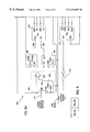
- FIG. 1 is a block diagram of data receivers according to the present invention.
- FIG. 2 is a timing diagram for the data receivers of FIG. 1 .
- FIG. 3 is a block diagram of clock recovery circuits and methods according to the present invention.
- FIG. 4 is a timing diagram for the clock recovery circuits and methods of FIG. 3 .
- FIG. 5 is a schematic diagram of clock recovery circuits and methods of FIG. 3 .
- FIG. 6 is a block diagram of clock recovery circuits and methods according to another aspect of the present invention.
- FIG. 7 is a schematic diagram of a fixed pulse generator of FIG. 6 .
- FIG. 8 is a block diagram of integrated circuits according to the present invention.
- data receiver 100 is responsive to multiple frequency input data 110 , including but not limited to ATM data that is received at 25 Mbps or 50 Mbps, to produce output data 120 .
- Data receiver 100 includes a D-type flip-flop 130 that includes a D input and a clock input (CLK).
- CLK clock input
- the multiple frequency input data 110 is coupled to the D input.
- a clock recovery circuit 140 is responsive to a mode signal 150 , to recover a clock from the multiple frequency input data 110 and provide the recovered clock 160 to the clock input of the D flip-flop 130 .
- FIG. 2 is a timing diagram illustrating multiple frequency input data 110 and the recovered clock 160 of FIG. 1 .
- the multiple frequency input data 110 may have a bit period of 31 nanoseconds or 15 nanoseconds, depending upon the frequency.
- the recovered clock is timed so that a positive going transition takes place at the mid-portion of each pulse of the multiple frequency input data, so that the data can be sampled appropriately.
- clock recovery circuit 140 ′ includes three main elements: a first phase locked loop (PLL1) 310 , a second phase locked loop (PLL2) 320 and a pulse generating and delaying circuit 330 .
- the first phase locked loop 310 generates a control signal 316 in response to a reference clock 311 .
- Pulse generating and delaying circuit 330 is responsive to the multiple frequency input data signal 110 and to a mode signal 150 , to generate from the input data signal pulses of predetermined width that are delayed by a predetermined delay. As shown in FIG. 3, both the predetermined width and the predetermined delay are a function of the mode signal.
- Second phase locked loop 320 is responsive to the control signal 316 from the first phase locked loop 310 and to the pulse generating and delaying circuit 330 , to generate a recovered clock signal 160 . Accordingly, the first phase locked loop 310 is independent of the mode signal and the second phase locked loop 320 and the pulse generating and delaying circuit 330 are both responsive to the mode signal 150 .
- clock recovery circuit 140 ′ of FIG. 3 A detailed description of clock recovery circuit 140 ′ of FIG. 3 will now be provided. However, it will be understood that each of the individual blocks of clock recovery circuit 140 ′ are conventional and the internal design of each block is well known to those having skill in the art. Accordingly, a description of the functionality of each block and of the interconnection of the blocks to provide a clock recovery circuit 140 ′ will be provided.
- first phase locked loop 310 includes a reference clock 311 which may include a crystal oscillator and supporting circuitry, and a first phase detector 312 .
- a first charge pump and loop filter 313 is responsive to the output of the first phase detector 312 .
- the output of the first charge pump and loop filter 313 is supplied as the control input of a first controlled oscillator, such as a first Voltage Controlled Oscillator (VCO) 314 .
- VCO Voltage Controlled Oscillator
- the output of first VCO 314 is applied to a divider 315 .
- the output of the divider is fed back as an input of first phase detector 312 .
- the reference clock 311 When clocking ATM data of 25 Mbps or 50 Mbps, the reference clock 311 may be set at 32 MHz and the divider 315 may be set to divide by four, so that the first VCO 314 oscillates at 128 MHz.
- the output of first charge pump and loop filter 313 which is applied to the control input of the first VCO, produces a control signal 316 .
- second phase locked loop 320 includes a second phase detector 322 , the output of which is applied to a second charge pump and loop filter 323 .
- the output of the second charge pump and loop filter 323 is applied as a control input to a second controlled oscillator such as a second VCO 324 .
- the control signal 316 is also applied as a control input to second VCO 324 .
- control signal 316 from the first phase locked loop 310 may be regarded as a “coarse tuning” input to second VCO 324 and the output of second charge pump and loop filter 323 may be regarded as a “fine tuning” control input for second VCO 324 .
- the output of second VCO 324 is applied to a variable divider 325 .
- the output of the variable divider 325 provides the recovered clock 160 .
- the variable divider is responsive to mode signal 150 .
- the mode signal 150 may set the variable divider 325 to divide by four when clocking 25 Mbps data, and to divide by two when clocking 50 Mbps data.
- pulse generating and delaying circuit 330 includes a pulse generator 332 that is responsive to the multiple frequency input data 110 and to the mode signal 150 , to generate a pulse having a pulse width that is a function of the mode signal, for each transition of the input data signal.
- a variable delay circuit 334 is responsive to the pulse generator 332 and to the mode signal 150 , to delay the pulses by a delay that is the function of the mode signal.
- the pulse generator may be set for 32 MHz output or 64 MHz output in response to the mode signal 150 , and the variable delay can provide twice the delay for 32 MHz operation as for 64 MHz operation.
- the output of the variable delay 324 is applied as an input to second phase detector 322 in second phase locked loop 320 .
- both the pulse generator 332 and the variable delay 334 are also responsive to the control signal 316 from the first phase locked loop 310 .
- clock recovery circuit 140 ′ also includes a gate 340 .
- the gate 340 is responsive to the pulse generator 332 and to the variable divider 325 .
- Gate 340 gates the variable frequency divider by the pulses from pulse generator 332 .
- the phase detector 322 is responsive to the variable frequency divider 325 , as gated by the gate 340 .
- multiple frequency input data 110 can use a Non-Return to Zero (NRZ) format, so that when multiple adjacent bits of the same value are present, there are no data transitions.
- the output of pulse generator 332 designated Rclki, is shown to generate a pulse for each transition of the multiple frequency input data 110 .
- the width of the pulse is selected as a function of the frequency of the input data.
- the width of the pulse is selected so that data can be clocked near the middle of an input data period, to obtain accurate sensing of the input data.
- the variable delay 334 operates on the output of pulse generator 332 (Rclki) to generate a delayed version of the pulses, designated as Clk 1 . Accordingly, as shown in FIG. 4, Clk 1 is delayed by a predetermined amount compared to Rclki.
- the amount of delay is a function of the mode signal, and is preferably selected so that the positive going transition in the signal Clk 1 is near the center of a bit of the multiple frequency input data 110 .
- the D-type flip-flop 130 of FIG. 1 can use a positive going transition in the recovered clock to clock the input data 110 .
- variable delay Clk 1 only provides positive going transitions for bits that include a transition.
- the third and fourth bits of multiple frequency input data 110 which are both zero, do not include a transition in waveform Clk 1 .
- waveform Clk 1 is applied to the second phase locked loop 320 .
- the output of variable divider 325 produces a recovered clock signal 160 that has a positive going transition near the center of every bit of the multiple frequency input data 110 .
- Second phase locked loop 320 maintains lock on the recovered clock signal 160 .
- Gate 340 reduces and preferably prevents loss of lock by eliminating control pulses to second VCO 324 , thus providing an output signal Clk 2 that maintains no phase difference with signal Clk 1 even in the absence of a pulse. Accordingly, erroneous control pulses to VCO 324 are reduced and preferably eliminated.
- a single first (master) phase locked loop 310 may be provided, that drives multiple second (slave) phase locked loops 320 and multiple pulse generating and delaying circuits 330 , to provide independently variable frequencies at each port. Accordingly, high performance and/or low cost multiple frequency clock recovery may be provided.
- FIG. 5 is a schematic diagram of a clock recovery circuit 140 ′ of FIG. 3 .
- pulse generator 332 may be implemented using a delay block 502 and an exclusive XOR gate 504 .
- a buffer 506 may be used to buffer multiple frequency input data 110 to provide buffered multiple frequency input data 110 ′ that can be applied to a D-type flip-flop, as shown in FIG. 1.
- a buffer 508 may also be used to buffer the recovered clock 160 to provide a buffered recovered clock 160 ′.
- Buffers 510 may be used to buffer the signal from the reference oscillator 311 that is applied to the first phase detector 312 .
- both the pulse generator 332 and the variable delay 334 may use variable delay blocks.
- a variable delay block is often implemented by a large number of delay stages, such as shift registers. Each stage provides a predetermined delay, so that the entire delay block is capable of providing a delay which is the sum of the delay of all of the stages. Thus, if each stage contributes a delay D s and there are n stages, the total delay of the delay block is given by n ⁇ D s .
- a variable number of stages is used in the delay block. Unfortunately, the need to provide appreciable delay may unduly increase the number of stages in the delay block.
- These large stage delay blocks may consume excessive area in an integrated circuit.
- a large delay block may be eliminated by providing a fixed pulse width.
- FIG. 6 illustrates a block diagram of a clock recovery circuit 140 ′′, wherein a pulse generating and delaying circuit 330 ′ includes a pulse generator 332 ′ that generates a pulse of fixed width, and a variable delay 334 that generates a variable delay. Since fixed pulse generator 332 ′ is fixed, it no longer needs to be responsive to mode signal 150 .
- FIG. 7 is a schematic diagram of an embodiment of a fixed pulse generator 332 ′ of FIG. 6 .
- fixed pulse generator 332 ′ may be implemented using resistors and capacitors to produce a desired delay using conventional resistor-capacitor (RC) time constants.
- RC resistor-capacitor
- two stages are provided. The first stage uses resistor R 1 and capacitors C 1 and C 2 . The second stage uses resistor R 2 and capacitors C 3 and C 4 . Buffers 702 , 704 and 706 are also used.
- the circuit of FIG. 7 can take up much less integrated circuit area than a pulse generator having many stages.
- Fixed pulse widths may be employed as shown in FIG. 6, rather than variable pulse widths as shown in FIG. 3, by selecting a pulse width that will allow the recovered clock to make a positive going transition in the middle of pulses of all the multiple frequency input data. Stated differently, the clock need not be sampled at the exact center of a bit of the input data, as long as the clock transition avoids the transitions of the input data signal.
- the pulse width of the pulse generator output need not be 50% of the operating frequency, as long as the pulse width does not exceed 50% of the period of the highest operating frequency of the clock recovery circuit. If the pulse width of the pulses generated by the pulse generator substantially exceeds 50% of the period of the highest operating frequency, it will not generate a pulse for every input data transition. Furthermore, because phase detection may be accomplished at the leading edge of the pulse, all that the delay of the pulse need accomplish is to place the leading edge of the pulse 25% through the data duration. This will have the same effect as centering a pulse of 50% duration. Because the actual data recovery clock has its own duty cycle independent of the pulse width, a 50% duty cycle may be achieved without a 50% duty cycle pulse.
- a fixed duration pulse may be utilized where the duration of the pulse is 50% of the period of the highest operating frequency.
- the same pulses may be used to generate signal C 1 k 1 for multiple frequency input data.
- Simplified pulse generators may be provided that are independent of the mode signal 150 .
- the variable delay 334 and variable divider 325 need be coupled to the mode signal 150 , as shown in FIG. 6 .
- an integrated circuit 800 can include a first (master) phase locked loop 310 that provides a control signal 316 to multiple second (slave) phase locked loops 320 i - 320 n and multiple pulse generating and delaying circuits 330 1 - 330 n .
- a corresponding plurality of input data ports 110 1 - 110 n and mode signals 150 1 - 150 n may be provided. Accordingly, a single first phase locked loop 310 may be used to provide a control signal 316 to multiple ports, each of which can independently receive input data of varying frequency.
Abstract
Description
Claims (29)
Priority Applications (1)
| Application Number | Priority Date | Filing Date | Title |
|---|---|---|---|
| US09/085,841 US6236697B1 (en) | 1998-05-28 | 1998-05-28 | Clock recovery for multiple frequency input data |
Applications Claiming Priority (1)
| Application Number | Priority Date | Filing Date | Title |
|---|---|---|---|
| US09/085,841 US6236697B1 (en) | 1998-05-28 | 1998-05-28 | Clock recovery for multiple frequency input data |
Publications (1)
| Publication Number | Publication Date |
|---|---|
| US6236697B1 true US6236697B1 (en) | 2001-05-22 |
Family
ID=22194304
Family Applications (1)
| Application Number | Title | Priority Date | Filing Date |
|---|---|---|---|
| US09/085,841 Expired - Lifetime US6236697B1 (en) | 1998-05-28 | 1998-05-28 | Clock recovery for multiple frequency input data |
Country Status (1)
| Country | Link |
|---|---|
| US (1) | US6236697B1 (en) |
Cited By (22)
| Publication number | Priority date | Publication date | Assignee | Title |
|---|---|---|---|---|
| US20020126786A1 (en) * | 2001-03-08 | 2002-09-12 | Cho James B. | Using phase interpolator information to detect a loss of lock condition during recovery of a clock signal from a received data stream |
| EP1271785A1 (en) * | 2001-06-27 | 2003-01-02 | Samsung Electronics Co., Ltd. | Noise-resistive, burst-mode receiving apparatus and method for recovering clock signal and data therefrom |
| US20030118137A1 (en) * | 2001-12-26 | 2003-06-26 | Skinner Harry G. | Spread spectrum clocking tolerant receivers |
| US20030193996A1 (en) * | 2002-04-10 | 2003-10-16 | International Business Machines Corporation | Transceiver for receiving and transmitting data over a network and method for testing the same |
| US20030214332A1 (en) * | 2002-05-20 | 2003-11-20 | Chih-Cheng Chen | Phase locked loop with low steady state phase errors and calibration circuit for the same |
| US20040035917A1 (en) * | 2002-08-22 | 2004-02-26 | Michel Koopmans | Apparatus and method for depositing and reflowing solder paste on a microelectronic workpiece |
| KR100467322B1 (en) * | 2002-09-18 | 2005-01-24 | 한국전자통신연구원 | Clock recovery Apparatus for burst mode signal and method of the same |
| US6900676B1 (en) * | 2002-08-27 | 2005-05-31 | Fujitsu Limited | Clock generator for generating accurate and low-jitter clock |
| KR100498229B1 (en) * | 2002-10-17 | 2005-07-01 | 광주과학기술원 | Apparatus for burst-mode clock and data recovery employing jitter reduction method |
| US20050213696A1 (en) * | 2003-05-01 | 2005-09-29 | Hirofumi Totsuka | Clock data recovery circuit |
| US7046093B1 (en) | 2003-08-27 | 2006-05-16 | Intergrated Device Technology, Inc. | Dynamic phase-locked loop circuits and methods of operation thereof |
| US7089444B1 (en) * | 2003-09-24 | 2006-08-08 | Altera Corporation | Clock and data recovery circuits |
| US20080038348A1 (en) * | 2005-06-27 | 2008-02-14 | Bioavail Laboratories International S.R.L. | Modified release formulations of a bupropion salt |
| US20090252258A1 (en) * | 2006-04-19 | 2009-10-08 | Panasonic Corporation | Pulse signal reception device, pulsed qpsk signal reception device, and pulse signal reception method |
| CN1953332B (en) * | 2005-10-17 | 2011-01-12 | 联芯科技有限公司 | Clock generator and communication terminal using the same |
| WO2011088610A1 (en) * | 2010-01-19 | 2011-07-28 | Integrated Device Technologies, Inc | Method and circuit for displayport video clock recovery |
| US20110188621A1 (en) * | 2010-02-04 | 2011-08-04 | Kazi Asaduzzaman | Clock and data recovery circuitry with auto-speed negotiation and other possible features |
| US20110249129A1 (en) * | 2010-04-09 | 2011-10-13 | Kinichi Ootsu | Transmission device, camera device, camera controller and camera system |
| CN106301358A (en) * | 2015-05-28 | 2017-01-04 | 瑞昱半导体股份有限公司 | The time pulse return apparatus of quick lock in and its method |
| WO2017039984A1 (en) * | 2015-09-01 | 2017-03-09 | Qualcomm Incorporated | Multiphase clock data recovery circuit calibration |
| US20180159219A1 (en) * | 2016-12-05 | 2018-06-07 | Infineon Technologies Ag | Device System and Method for Radio Frequency Signal Path Calibration |
| US20190207611A1 (en) * | 2017-12-29 | 2019-07-04 | Texas Instruments Incorporated | Phased locked loop integrated circuit |
Citations (6)
| Publication number | Priority date | Publication date | Assignee | Title |
|---|---|---|---|---|
| US3993868A (en) * | 1974-08-19 | 1976-11-23 | Rca Corporation | Minimum shift keying communication system |
| US4912566A (en) * | 1988-01-06 | 1990-03-27 | Dainippon Screen Mfg. Co., Ltd. | Image recording apparatus with a variable magnification capable of finely changing an image magnification |
| USRE34317E (en) * | 1982-08-05 | 1993-07-20 | Seiko Epson Corporation | Variable frequency oscillator |
| US5671258A (en) | 1994-12-20 | 1997-09-23 | 3Com Corporation | Clock recovery circuit and receiver using same |
| US5689692A (en) | 1992-12-23 | 1997-11-18 | Honeywell Inc. | Method and apparatus for decoding an encoded NRZ signal |
| US6094236A (en) * | 1996-04-26 | 2000-07-25 | Kabushiki Kaisha Toshiba | Tuner circuit |
-
1998
- 1998-05-28 US US09/085,841 patent/US6236697B1/en not_active Expired - Lifetime
Patent Citations (6)
| Publication number | Priority date | Publication date | Assignee | Title |
|---|---|---|---|---|
| US3993868A (en) * | 1974-08-19 | 1976-11-23 | Rca Corporation | Minimum shift keying communication system |
| USRE34317E (en) * | 1982-08-05 | 1993-07-20 | Seiko Epson Corporation | Variable frequency oscillator |
| US4912566A (en) * | 1988-01-06 | 1990-03-27 | Dainippon Screen Mfg. Co., Ltd. | Image recording apparatus with a variable magnification capable of finely changing an image magnification |
| US5689692A (en) | 1992-12-23 | 1997-11-18 | Honeywell Inc. | Method and apparatus for decoding an encoded NRZ signal |
| US5671258A (en) | 1994-12-20 | 1997-09-23 | 3Com Corporation | Clock recovery circuit and receiver using same |
| US6094236A (en) * | 1996-04-26 | 2000-07-25 | Kabushiki Kaisha Toshiba | Tuner circuit |
Cited By (49)
| Publication number | Priority date | Publication date | Assignee | Title |
|---|---|---|---|---|
| US20020126786A1 (en) * | 2001-03-08 | 2002-09-12 | Cho James B. | Using phase interpolator information to detect a loss of lock condition during recovery of a clock signal from a received data stream |
| US6856661B2 (en) * | 2001-03-08 | 2005-02-15 | Texas Instruments Incorporated | Using phase interpolator information to detect a loss of lock condition during recovery of a clock signal from a received data stream |
| EP1271785A1 (en) * | 2001-06-27 | 2003-01-02 | Samsung Electronics Co., Ltd. | Noise-resistive, burst-mode receiving apparatus and method for recovering clock signal and data therefrom |
| US20030026373A1 (en) * | 2001-06-27 | 2003-02-06 | Samsung Electronics Co., Ltd. | Noise-resistive, burst-mode receiving apparatus and a method for recovering a clock signal and data therefrom |
| US7177381B2 (en) * | 2001-06-27 | 2007-02-13 | Samsung Electronics Co., Ltd. | Noise-resistive, burst-mode receiving apparatus and a method for recovering a clock signal and data therefrom |
| US20030118137A1 (en) * | 2001-12-26 | 2003-06-26 | Skinner Harry G. | Spread spectrum clocking tolerant receivers |
| US6937679B2 (en) * | 2001-12-26 | 2005-08-30 | Intel Corporation | Spread spectrum clocking tolerant receivers |
| US7760796B2 (en) | 2002-04-10 | 2010-07-20 | International Business Machines Corporation | Transceiver for receiving and transmitting data over a network and method for testing the same |
| US20030193996A1 (en) * | 2002-04-10 | 2003-10-16 | International Business Machines Corporation | Transceiver for receiving and transmitting data over a network and method for testing the same |
| US20090003419A1 (en) * | 2002-04-10 | 2009-01-01 | Iadanza Joseph A | Transceiver for receiving and transmitting data over a network and method for testing the same |
| US7313178B2 (en) * | 2002-04-10 | 2007-12-25 | International Business Machines Corporation | Transceiver for receiving and transmitting data over a network and method for testing the same |
| US20030214332A1 (en) * | 2002-05-20 | 2003-11-20 | Chih-Cheng Chen | Phase locked loop with low steady state phase errors and calibration circuit for the same |
| US6897691B2 (en) * | 2002-05-20 | 2005-05-24 | Mediatek Inc. | Phase locked loop with low steady state phase errors and calibration circuit for the same |
| US20040035917A1 (en) * | 2002-08-22 | 2004-02-26 | Michel Koopmans | Apparatus and method for depositing and reflowing solder paste on a microelectronic workpiece |
| US6900676B1 (en) * | 2002-08-27 | 2005-05-31 | Fujitsu Limited | Clock generator for generating accurate and low-jitter clock |
| KR100467322B1 (en) * | 2002-09-18 | 2005-01-24 | 한국전자통신연구원 | Clock recovery Apparatus for burst mode signal and method of the same |
| KR100498229B1 (en) * | 2002-10-17 | 2005-07-01 | 광주과학기술원 | Apparatus for burst-mode clock and data recovery employing jitter reduction method |
| US7489757B2 (en) * | 2003-05-01 | 2009-02-10 | Mitsubishi Denki Kabushiki Kaisha | Clock data recovery circuit |
| US20050213696A1 (en) * | 2003-05-01 | 2005-09-29 | Hirofumi Totsuka | Clock data recovery circuit |
| US7046093B1 (en) | 2003-08-27 | 2006-05-16 | Intergrated Device Technology, Inc. | Dynamic phase-locked loop circuits and methods of operation thereof |
| US7089444B1 (en) * | 2003-09-24 | 2006-08-08 | Altera Corporation | Clock and data recovery circuits |
| US20080038348A1 (en) * | 2005-06-27 | 2008-02-14 | Bioavail Laboratories International S.R.L. | Modified release formulations of a bupropion salt |
| US9504640B2 (en) | 2005-06-27 | 2016-11-29 | Valeant Pharmaceuticals Luxembourg S.Á.R.L. | Modified release formulations of a bupropion salt |
| US8932628B2 (en) | 2005-06-27 | 2015-01-13 | Valeant International Bermuda | Modified release formulations of a bupropion salt |
| CN1953332B (en) * | 2005-10-17 | 2011-01-12 | 联芯科技有限公司 | Clock generator and communication terminal using the same |
| US20090252258A1 (en) * | 2006-04-19 | 2009-10-08 | Panasonic Corporation | Pulse signal reception device, pulsed qpsk signal reception device, and pulse signal reception method |
| US8130883B2 (en) * | 2006-04-19 | 2012-03-06 | Panasonic Corporation | Pulse signal reception device, pulsed QPSK signal reception device, and pulse signal reception method |
| WO2011088610A1 (en) * | 2010-01-19 | 2011-07-28 | Integrated Device Technologies, Inc | Method and circuit for displayport video clock recovery |
| US8217689B2 (en) | 2010-01-19 | 2012-07-10 | Integrated Device Technology, Inc. | Method and circuit for DisplayPort video clock recovery |
| US8811555B2 (en) | 2010-02-04 | 2014-08-19 | Altera Corporation | Clock and data recovery circuitry with auto-speed negotiation and other possible features |
| US8829958B2 (en) | 2010-02-04 | 2014-09-09 | Altera Corporation | Clock and data recovery circuitry with auto-speed negotiation and other possible features |
| WO2011097442A1 (en) * | 2010-02-04 | 2011-08-11 | Altera Corporation | Clock and data recovery circuitry with auto-speed negotiation and other possible features |
| US20110188621A1 (en) * | 2010-02-04 | 2011-08-04 | Kazi Asaduzzaman | Clock and data recovery circuitry with auto-speed negotiation and other possible features |
| US8558905B2 (en) * | 2010-04-09 | 2013-10-15 | Sony Corporation | Transmission device and camera device operating with serial signals corresponding to clock signals having different frequencies |
| US20110249129A1 (en) * | 2010-04-09 | 2011-10-13 | Kinichi Ootsu | Transmission device, camera device, camera controller and camera system |
| CN106301358B (en) * | 2015-05-28 | 2019-01-01 | 瑞昱半导体股份有限公司 | The time pulse return apparatus of quick lock in and its method |
| CN106301358A (en) * | 2015-05-28 | 2017-01-04 | 瑞昱半导体股份有限公司 | The time pulse return apparatus of quick lock in and its method |
| TWI572142B (en) * | 2015-05-28 | 2017-02-21 | 瑞昱半導體股份有限公司 | Burst mode clock data recovery device and method thereof |
| EP3678323A1 (en) * | 2015-09-01 | 2020-07-08 | QUALCOMM Incorporated | Multiphase clock data recovery circuit calibration |
| WO2017039984A1 (en) * | 2015-09-01 | 2017-03-09 | Qualcomm Incorporated | Multiphase clock data recovery circuit calibration |
| CN112751660A (en) * | 2015-09-01 | 2021-05-04 | 高通股份有限公司 | Method and apparatus for multi-phase clock data recovery circuit calibration |
| CN112751660B (en) * | 2015-09-01 | 2024-03-08 | 高通股份有限公司 | Method and apparatus for multiphase clock data recovery circuit calibration |
| CN108155956A (en) * | 2016-12-05 | 2018-06-12 | 英飞凌科技股份有限公司 | For the equipment, system and method for RF signal path calibration |
| US20180159219A1 (en) * | 2016-12-05 | 2018-06-07 | Infineon Technologies Ag | Device System and Method for Radio Frequency Signal Path Calibration |
| US10862207B2 (en) * | 2016-12-05 | 2020-12-08 | Infineon Technologies Ag | Device system and method for radio frequency signal path calibration |
| CN108155956B (en) * | 2016-12-05 | 2021-10-29 | 英飞凌科技股份有限公司 | Apparatus, system and method for radio frequency signal path calibration |
| US20190207611A1 (en) * | 2017-12-29 | 2019-07-04 | Texas Instruments Incorporated | Phased locked loop integrated circuit |
| US10560109B2 (en) * | 2017-12-29 | 2020-02-11 | Texas Instruments Incorporated | Phased locked loop integrated circuit |
| US10879913B2 (en) | 2017-12-29 | 2020-12-29 | Texas Instruments Incorporated | Phased locked loop integrated circuit |
Similar Documents
| Publication | Publication Date | Title |
|---|---|---|
| US6236697B1 (en) | Clock recovery for multiple frequency input data | |
| US7684531B2 (en) | Data recovery method and data recovery circuit | |
| US5850422A (en) | Apparatus and method for recovering a clock signal which is embedded in an incoming data stream | |
| US5689533A (en) | Refined timing recovery circuit | |
| US5633899A (en) | Phase locked loop for high speed data capture of a serial data stream | |
| EP0244122B1 (en) | Clock recovery digital phase-locked loop | |
| US5812619A (en) | Digital phase lock loop and system for digital clock recovery | |
| EP0494984B1 (en) | Phase detector for phase-locked loop clock recovery system | |
| EP0523886B1 (en) | Phase error processor | |
| US7913104B1 (en) | Method and apparatus for receive channel data alignment with minimized latency variation | |
| US5909130A (en) | Digital lock detector for phase-locked loop | |
| GB2091961A (en) | Phase tolerant bit synchronizer for digital signals | |
| KR0153952B1 (en) | Apparatus for retiming high speed digital data | |
| EP1441443A2 (en) | Digital phase locked loop circuitry and methods | |
| US5761255A (en) | Edge-synchronized clock recovery unit | |
| US5864250A (en) | Non-servo clock and data recovery circuit and method | |
| WO1999022482A1 (en) | Clock recovery circuit | |
| US5694062A (en) | Self-timed phase detector and method | |
| EP0663744B1 (en) | Signal processing device having PLL circuits | |
| JPH07202874A (en) | Cmos technology high speed digital signal transceiver | |
| KR950008461B1 (en) | Apparatus for synchronising nrz data bit | |
| US6670853B2 (en) | Data recovery circuit and method thereof | |
| US6314151B1 (en) | Phase comparator operable at half frequency of input signal | |
| US6748027B1 (en) | CMI signal timing recovery | |
| EP0897229A2 (en) | Clock recovery circuit |
Legal Events
| Date | Code | Title | Description |
|---|---|---|---|
| AS | Assignment |
Owner name: INTEGRATED DEVICE TECHNOLOGY, INC., CALIFORNIA Free format text: ASSIGNMENT OF ASSIGNORS INTEREST;ASSIGNOR:FANG, AL X.;REEL/FRAME:009221/0849 Effective date: 19980527 |
|
| STCF | Information on status: patent grant |
Free format text: PATENTED CASE |
|
| FEPP | Fee payment procedure |
Free format text: PAYOR NUMBER ASSIGNED (ORIGINAL EVENT CODE: ASPN); ENTITY STATUS OF PATENT OWNER: LARGE ENTITY |
|
| FPAY | Fee payment |
Year of fee payment: 4 |
|
| FPAY | Fee payment |
Year of fee payment: 8 |
|
| FPAY | Fee payment |
Year of fee payment: 12 |
|
| AS | Assignment |
Owner name: JPMORGAN CHASE BANK, N.A., AS COLLATERAL AGENT, NE Free format text: SECURITY AGREEMENT;ASSIGNORS:INTEGRATED DEVICE TECHNOLOGY, INC.;GIGPEAK, INC.;MAGNUM SEMICONDUCTOR, INC.;AND OTHERS;REEL/FRAME:042166/0431 Effective date: 20170404 Owner name: JPMORGAN CHASE BANK, N.A., AS COLLATERAL AGENT, NEW YORK Free format text: SECURITY AGREEMENT;ASSIGNORS:INTEGRATED DEVICE TECHNOLOGY, INC.;GIGPEAK, INC.;MAGNUM SEMICONDUCTOR, INC.;AND OTHERS;REEL/FRAME:042166/0431 Effective date: 20170404 |
|
| AS | Assignment |
Owner name: INTEGRATED DEVICE TECHNOLOGY, INC., CALIFORNIA Free format text: RELEASE BY SECURED PARTY;ASSIGNOR:JPMORGAN CHASE BANK, N.A.;REEL/FRAME:048746/0001 Effective date: 20190329 Owner name: MAGNUM SEMICONDUCTOR, INC., CALIFORNIA Free format text: RELEASE BY SECURED PARTY;ASSIGNOR:JPMORGAN CHASE BANK, N.A.;REEL/FRAME:048746/0001 Effective date: 20190329 Owner name: CHIPX, INCORPORATED, CALIFORNIA Free format text: RELEASE BY SECURED PARTY;ASSIGNOR:JPMORGAN CHASE BANK, N.A.;REEL/FRAME:048746/0001 Effective date: 20190329 Owner name: GIGPEAK, INC., CALIFORNIA Free format text: RELEASE BY SECURED PARTY;ASSIGNOR:JPMORGAN CHASE BANK, N.A.;REEL/FRAME:048746/0001 Effective date: 20190329 Owner name: ENDWAVE CORPORATION, CALIFORNIA Free format text: RELEASE BY SECURED PARTY;ASSIGNOR:JPMORGAN CHASE BANK, N.A.;REEL/FRAME:048746/0001 Effective date: 20190329 |