WO2025141925A1 - 半導体パッケージ - Google Patents
半導体パッケージ Download PDFInfo
- Publication number
- WO2025141925A1 WO2025141925A1 PCT/JP2024/027079 JP2024027079W WO2025141925A1 WO 2025141925 A1 WO2025141925 A1 WO 2025141925A1 JP 2024027079 W JP2024027079 W JP 2024027079W WO 2025141925 A1 WO2025141925 A1 WO 2025141925A1
- Authority
- WO
- WIPO (PCT)
- Prior art keywords
- wiring
- component
- layer
- main surface
- semiconductor package
- Prior art date
- Legal status (The legal status is an assumption and is not a legal conclusion. Google has not performed a legal analysis and makes no representation as to the accuracy of the status listed.)
- Pending
Links
Images





Classifications
-
- H—ELECTRICITY
- H01—ELECTRIC ELEMENTS
- H01F—MAGNETS; INDUCTANCES; TRANSFORMERS; SELECTION OF MATERIALS FOR THEIR MAGNETIC PROPERTIES
- H01F27/00—Details of transformers or inductances, in general
- H01F27/06—Mounting, supporting or suspending transformers, reactors or choke coils not being of the signal type
-
- H—ELECTRICITY
- H05—ELECTRIC TECHNIQUES NOT OTHERWISE PROVIDED FOR
- H05K—PRINTED CIRCUITS; CASINGS OR CONSTRUCTIONAL DETAILS OF ELECTRIC APPARATUS; MANUFACTURE OF ASSEMBLAGES OF ELECTRICAL COMPONENTS
- H05K3/00—Apparatus or processes for manufacturing printed circuits
- H05K3/46—Manufacturing multilayer circuits
-
- H—ELECTRICITY
- H10—SEMICONDUCTOR DEVICES; ELECTRIC SOLID-STATE DEVICES NOT OTHERWISE PROVIDED FOR
- H10W—GENERIC PACKAGES, INTERCONNECTIONS, CONNECTORS OR OTHER CONSTRUCTIONAL DETAILS OF DEVICES COVERED BY CLASS H10
- H10W70/00—Package substrates; Interposers; Redistribution layers [RDL]
- H10W70/60—Insulating or insulated package substrates; Interposers; Redistribution layers
-
- H—ELECTRICITY
- H10—SEMICONDUCTOR DEVICES; ELECTRIC SOLID-STATE DEVICES NOT OTHERWISE PROVIDED FOR
- H10W—GENERIC PACKAGES, INTERCONNECTIONS, CONNECTORS OR OTHER CONSTRUCTIONAL DETAILS OF DEVICES COVERED BY CLASS H10
- H10W90/00—Package configurations
Definitions
- the above configuration allows passive components that have been determined to pass to be mounted, improving reliability.
- the axis perpendicular to the first main surface 10A is defined as the first axis X.
- a specific direction along the first axis X is defined as the first positive direction X1
- the direction opposite to the first positive direction X1 is defined as the first negative direction X2.
- the first positive direction X1 coincides with the direction in which the first main surface 10A faces.
- the first negative direction X2 coincides with the direction in which the second main surface 10B faces.
- the semiconductor package 10 includes a second layer L2, a third layer L3, a fourth layer L4, and a fifth layer L5 stacked on a first layer L1.
- the outer shape of each of the first layer L1 to the fifth layer L5 is rectangular.
- the layers of the semiconductor package 10 are arranged in the following order from the first negative direction X2 side to the first positive direction X1 side: second layer L2, first layer L1, third layer L3, fourth layer L4, and fifth layer L5.
- the first layer L1 has a first sealing portion 11, a plurality of first electronic components 12, a plurality of first via wirings 14, and a plurality of first component external terminals 15.
- the first layer L1 is a first component layer that includes the first electronic components 12.
- the outer shape of the first sealing portion 11 is a substantially rectangular parallelepiped.
- the plane of the outer surface of the first sealing portion 11 facing the first positive direction X1 is the first main surface 10A.
- the plane of the outer surface of the first sealing portion 11 facing the first negative direction X2 is the second main surface 10B.
- the first sealing portion 11 is TEOS (Tetra EthOxy Silane). That is, the first sealing portion 11 contains an inorganic material.
- SiO 2 , TiN, TiO, SiCOH, etc. can be adopted as the material containing the inorganic material applied to the first sealing portion 11.
- the first electronic component 12 is either a passive component or an active component.
- a passive component is either an inductor, resistor, or capacitor.
- An active component is an electronic component that performs an active task such as amplifying, rectifying, or converting current.
- active components are diodes, transistors, and integrated circuits that include these. Note that even if the integrated circuit includes an inductor, resistor, and capacitor, it is treated as an active component as long as it has at least one active component.
- “electronic component” refers to either a passive component or an active component.
- the first layer L1 has three first electronic components 12.
- the three first electronic components 12 are two active components 12A and one passive component 12B. That is, at least one of the first electronic components 12 is an active component 12A. Also, one of the first electronic components 12 is a passive component 12B.
- Passive component 12B contains inorganic materials.
- passive component 12B is an inductor
- passive component 12B contains inorganic materials such as Fe, FeSi, and chromium-zirconium-tantalum alloys. These materials are contained in the core of the inductor.
- passive component 12B is an inductor
- passive component 12B contains inorganic materials such as Cu, Ag, and the like. These materials are contained in the wiring of the inductor.
- the passive component 12B when the passive component 12B is a capacitor, the passive component 12B contains materials such as SiO 2 , SiN, barium titanate, etc. as inorganic materials. These materials are contained in the core of the capacitor. Furthermore, when the passive component 12B is a capacitor, the passive component 12B contains materials such as Al, Ni, etc. These materials are contained in the electrodes. Note that the passive component 12B, whether it is an inductor or a capacitor, contains epoxy-based and polyimide-based resins, etc. as organic materials.
- Each of the first electronic components 12 is located inside the first sealing portion 11. Specifically, the three first electronic components 12 are lined up in a direction parallel to the first main surface 10A. Furthermore, each of the first electronic components 12 is located inside the first layer L1, closer to the second main surface 10B. Specifically, one main surface of each of the first electronic components 12 is generally flush with the second main surface 10B of the first layer L1.
- the two active components 12A have the same maximum dimension in a direction perpendicular to the first main surface 10A.
- the maximum dimension of the remaining first electronic component 12, the passive component 12B, in a direction perpendicular to the first main surface 10A is greater than the maximum dimension of each active component 12A in a direction perpendicular to the first main surface 10A.
- Each active component 12A includes a component body 12M, a connection terminal 13, and an internal terminal 13A.
- the connection terminal 13 functions as an external terminal for connecting the first electronic component 12 to external wiring or the like of the first electronic component 12.
- each active component 12A has two connection terminals 13 and two internal terminals 13A.
- the two connection terminals 13 are exposed toward the first negative direction X2.
- each connection terminal 13 protrudes from the component body 12M.
- each connection terminal 13 is exposed from the first sealing portion 11 on the second main surface 10B side of the first sealing portion 11. Furthermore, each of these connection terminals 13 protrudes from the first sealing portion 11.
- the volume fraction of Cu on the outer surface of the connection terminal 13 of each first electronic component 12 is 50 vol% or more. In the first embodiment, the volume fraction of Cu in the entirety of each connection terminal 13 is 90 vol% or more. In addition to the Cu component, each connection terminal 13 contains small amounts of S, Ni, and O components.
- the two internal terminals 13A are exposed from the component body 12M toward the first positive direction X1. That is, each internal terminal 13A is exposed from the component body 12M on the opposite side to the connection terminal 13 in the direction perpendicular to the first main surface 10A. In the example shown in FIG. 1, the internal terminals 13A do not protrude from the component body 12M. In other words, the end face of the internal terminal 13A on the first positive direction X1 side is flush with the component body 12M. That is, the protrusion amount of the connection terminal 13 is greater than the protrusion amount of the internal terminal 13A.
- the material of each internal terminal 13A is the same as the material of the connection terminal 13.
- the passive component 12B of the first electronic component 12 has two connection terminals 13.
- the material of the two connection terminals 13 is the same as the material of the connection terminals 13 of the active component 12A.
- the two connection terminals 13 are exposed toward the first negative direction X2 side.
- each connection terminal 13 on the first negative direction X2 side is exposed from the first sealing portion 11 on the second main surface 10B side of the first sealing portion 11.
- each connection terminal 13 on the first negative direction X2 side protrudes from the first sealing portion 11. In this way, the connection terminals 13 of each first electronic component 12 are exposed from the first sealing portion 11 only on the second main surface 10B of the first sealing portion 11.
- the first layer L1 has four first via wirings 14.
- Each first via wiring 14 is approximately cylindrical.
- Each first via wiring 14 extends in a direction intersecting the first main surface 10A inside the first sealing portion 11.
- each first via wiring 14 extends in a direction perpendicular to the first main surface 10A.
- a first end of each first via wiring 14 is connected to an internal terminal 13A in the active component 12A.
- a second end of each first via wiring 14 is exposed from the first sealing portion 11. That is, an end of the first via wiring 14 is exposed from the first sealing portion 11 on the first main surface 10A.
- the first via wiring 14 contains a Cu component.
- the volume fraction of Cu in the first via wiring 14 is 50 vol% or more.
- the volume fraction of Cu in the first wiring portion 22 is 90 vol% or more.
- the first component external terminals 15 protrude from the first sealing portion 11. Specifically, the first component external terminals 15 are exposed from the first positive direction X1 side of the first sealing portion 11. Each first component external terminal 15 is connected to the second end of the first via wiring 14. The material of each first component external terminal 15 is the same as the material of the first via wiring 14.
- the second layer L2 is stacked on the first negative direction X2 side with respect to the first layer L1.
- the second layer L2 is stacked directly on the second main surface 10B of the first layer L1. Therefore, the second layer L2 is adjacent to the first component layer in a direction perpendicular to the first main surface 10A.
- the second layer L2 has a first insulating resin portion 21, a first wiring portion 22, and a plurality of first wiring external terminals 23. Therefore, the second layer L2 is a first wiring layer including the first wiring portion 22.
- the outer shape of the first insulating resin part 21 is a substantially rectangular parallelepiped.
- the outer shape of the first insulating resin part 21 substantially matches the outer shape of the second layer L2.
- the material of the first insulating resin part 21 is a synthetic resin containing an inorganic filler.
- the synthetic resin is, for example, an epoxy-based or polyimide-based resin.
- the first insulating resin part 21 covers the peripheral surface of the connection terminal 13 of the first electronic component 12 protruding from the first sealing part 11.
- the first wiring portion 22 has a plurality of first columnar wirings 22B extending in a direction intersecting the first main surface 10A, and a plurality of first wirings 22A extending in a direction parallel to the first main surface 10A.
- the first columnar wirings 22B are connected to the first wirings 22A.
- the plurality of first columnar wirings 22B and the plurality of first wirings 22A are connected to each other. Note that in FIG. 1, only some of the first columnar wirings 22B and some of the first wirings 22A are labeled with reference numerals.
- the first wiring portion 22 is connected to the connection terminal 13 of the first electronic component 12.
- the first wiring portion 22 extends inside the first insulating resin portion 21 in an arbitrary pattern.
- the material of the first wiring portion 22 is the same as the material of the first via wiring 14. In other words, the volume fraction of Cu in the first wiring portion 22 is 50 vol% or more.
- the third layer L3 has a second insulating resin portion 31, a second wiring portion 32, and a plurality of second wiring external terminals 33.
- the third layer L3 is a second wiring layer including the second wiring portion 32.
- the second insulating resin portion 31 has a generally rectangular parallelepiped shape. The shape of the second insulating resin portion 31 generally matches the shape of the third layer L3.
- the second insulating resin portion 31 is made of a synthetic resin containing an inorganic filler. The second insulating resin portion 31 covers the peripheral surfaces of the first component external terminals 15.
- the second wiring portion 32 has a plurality of second wirings 32A extending in a direction parallel to the first main surface 10A, and a plurality of second columnar wirings 32B extending in a direction intersecting the first main surface 10A.
- the second columnar wirings 32B are connected to the second wirings 32A.
- the plurality of second columnar wirings 32B and the plurality of second wirings 32A are connected to each other. Note that in FIG. 1, only some of the second columnar wirings 32B and some of the second wirings 32A are labeled with reference numerals.
- the second wiring portion 32 is connected to the first component external terminal 15. That is, the second wiring portion 32 is connected to the first via wiring 14 in the first layer L1 via the first component external terminal 15. In other words, the second end of the first via wiring 14 is connected to the second wiring portion 32 in the second wiring layer.
- the second wiring portion 32 extends inside the second insulating resin portion 31 in an arbitrary pattern.
- the material of the second wiring portion 32 is the same as the material of the first wiring portion 22. That is, the volume fraction of Cu in the second wiring portion 32 is 50 vol% or more.
- the second wiring external terminals 33 protrude from the second insulating resin part 31. Specifically, the second wiring external terminals 33 are exposed from the first positive direction X1 side of the second insulating resin part 31.
- the material of each second wiring external terminal 33 is the same as the material of the first component external terminal 15.
- the fourth layer L4 is stacked on the first positive direction X1 side with respect to the third layer L3.
- the fourth layer L4 has a second sealing portion 41, a plurality of second electronic components 42, a second via wiring 44, a plurality of second component external terminals 45, a plurality of connection portions 47, and an underfill 46.
- the fourth layer L4 is a second component layer that includes the second electronic components 42.
- the second sealing portion 41 has a substantially rectangular parallelepiped shape and is substantially the same as the fourth layer L4.
- the second sealing portion 41 is made of a synthetic resin containing an inorganic filler.
- the fourth layer L4 includes three second electronic components 42.
- the second electronic components 42 are two active components 42A and one passive component 42B. That is, at least one of the second electronic components 42 is the active component 42A. Also, one of the second electronic components 42 is the passive component 42B.
- the volume fraction of the inorganic material in the passive component 42B is 80 vol% or more.
- Each of the second electronic components 42 is located inside the second sealing portion 41. Specifically, the three second electronic components 42 are lined up in a direction parallel to the first main surface 10A. Each second electronic component 42 includes a connection terminal 43.
- the connection terminal 43 functions as an external terminal for connecting the second electronic component 42 to an external wiring or the like of the second electronic component 42.
- each second electronic component 42 has two connection terminals 43.
- Each connection terminal 43 is exposed toward the first negative direction X2. These connection terminals 43 are not covered by the second insulating resin part 31.
- the material of the connection terminals 43 of each second electronic component 42 is the same as the material of the connection terminals 43 of the first electronic component 12.
- the first sealing portion 11 is formed. Specifically, first, an insulator is formed from the first positive direction X1 side of each first electronic component 12 and the first release layer RL1 by a known technique such as a CVD method. The material of the insulator is TEOS. Next, a first through hole PO1 is formed in the insulator by a known technique such as the Bosch method. The first through hole PO1 is formed at a position overlapping with the internal terminal 13A of the first electronic component 12 when viewed in the first negative direction X2.
- the first layer L1 has three first electronic components 22. All three first electronic components 22 are active components. That is, at least one of the first electronic components 22 is an active component.
- first wiring layers LN1 Two of the three first electronic components 22 are adjacent to different first wiring layers LN1. Specifically, a first wiring layer LN1 is laminated on each of the surfaces of the two first electronic components 22 facing the first positive direction X1. Note that the first wiring layers LN1 are not electrically connected to each other within the first layer L1.
- Each first electronic component 22 has a connection terminal 26.
- the connection terminal 26 functions as an external terminal for connecting the first electronic component 22 to external wiring or the like of the first electronic component 22.
- each first electronic component 22 has a plurality of connection terminals 26.
- Each connection terminal 26 is exposed toward the first negative direction X2.
- Each connection terminal 26 is exposed from the first sealing portion 21 on the second main surface 10B side of the first sealing portion 21.
- Each connection terminal 26 protrudes from the first sealing portion 21.
- the volume fraction of Cu in the outer surface of each connection terminal 26 is 50 vol% or more.
- the material of the connection terminals 26 in the second embodiment is the same as that in the first embodiment.
- Each first wiring layer LN1 has a first wiring portion 12 and a first insulating resin portion 11.
- the first wiring portion 12 and the first insulating resin portion 11 inside the first wiring layer LN1 are omitted.
- the first wiring portion 12 and the first insulating resin portion 11 have the same configuration as in the first embodiment. That is, the outer shape of each first insulating resin portion 11 is substantially rectangular. However, the dimension of each first insulating resin portion 11 in a direction parallel to the first main surface 10A is smaller than the dimension of each first layer L1 in a direction parallel to the first main surface 10A.
- each first insulating resin portion 11 in a direction perpendicular to the first main surface 10A is smaller than the dimension of each first layer L1 in a direction perpendicular to the first main surface 10A.
- the material of each first insulating resin portion 11 is a synthetic resin containing an inorganic filler.
- Two first electronic components 22 adjacent to the first wiring layer LN1 are provided with through-wires 23. That is, one or more selected from the active components are provided with through-wires 23. Each active component is provided with two through-wires 23. Each through-wire 23 is substantially cylindrical. Each through-wire 23 penetrates the active component in a direction perpendicular to the first main surface 10A. The end of each through-wire 23 on the first positive direction X1 side is connected to the first wiring portion 12 of the first wiring layer LN1. Also, the end of each through-wire 23 on the first negative direction X2 side is connected to the connection terminal 26.
- the first component layer PT1 has four first via wirings 24.
- Each first via wiring 24 is approximately cylindrical.
- the diameter of each first via wiring 24 is larger than the diameter of each through wiring 23.
- the maximum dimension of the through wiring 23 in a direction parallel to the first main surface 10A is smaller than the maximum dimension of the first via wiring 24 in a direction parallel to the first main surface 10A.
- Each first via wiring 24 extends in a direction intersecting the first main surface 10A inside the first sealing portion 21. In the second embodiment, each first via wiring 24 extends in a direction perpendicular to the first main surface 10A.
- Two of the four first via wirings 24 extend from the first wiring layer LN1. That is, a first end of the first via wiring 24 on the first negative direction X2 side is connected to the first wiring portion 12 of the first wiring layer LN1. In addition, a second end of the first via wiring 24 on the first positive direction X1 side is exposed from the first sealing portion 21 on the first main surface 10A side.
- first ends of the remaining two first via wirings 24 on the first negative direction X2 side are exposed from the first sealing portion 21 on the second main surface 10B side.
- second ends of the two first via wirings 24 on the first positive direction X1 side are exposed from the first sealing portion 21 on the first main surface 10A side. That is, the ends of the four first via wirings 24 in the second embodiment are exposed from the first sealing portion 21 on the first main surface 10A side.
- the first via wiring 24 contains a Cu component.
- the volume fraction of Cu in the first via wiring 24 is 50 vol% or more.
- the volume fraction of Cu in the first via wiring 24 is 90 vol% or more.
- the first layer L1 has ten first component external terminals 25.
- the first layer L1 may have other first component external terminals 25 that are not shown in the cross section of FIG. 12. Two of these first component external terminals 25 protrude from the first negative direction X2 side of the first sealing portion 21.
- Each of the first component external terminals 25 is connected to a first end of the first via wiring 24 exposed from the first sealing portion 21 on the second main surface 10B side.
- the material of these ten first component external terminals 25 is the same as the material of the connection terminal 26.
- the remaining eight first component external terminals 25 among the first component external terminals 25 on the cross section shown in FIG. 12 are exposed on the first positive direction X1 side of the first sealing portion 21.
- the peripheral surfaces of the eight first component external terminals 25 are covered by the first sealing portion 21.
- Four of these first component external terminals 25 are connected to the ends of the first via wiring 24 on the first positive direction X1 side.
- the remaining four first component external terminals 25 are directly stacked on the first positive direction X1 side of the first wiring layer LN1.
- the first component external terminals 25 are electrically connected to the first wiring portion 12 in the first wiring layer LN1.
- the material of these eight first component external terminals 25 is the same as the material of the first wiring portion 12. Note that in FIG. 12, only some of the first component external terminals 25 are labeled with reference numerals.
- the second layer L2 is directly stacked on the first positive direction X1 side of the first layer L1.
- the second layer L2 includes a second component layer PT2 and four second wiring layers LN2.
- the second layer L2 also includes a second wiring layer LN2, which is a layer separate from the second component layer PT2, that is embedded inside the second component layer PT2.
- the second component layer PT 2 has a second sealing portion 41 , a plurality of second electronic components 42 , and a plurality of second component external terminals 43 .
- the outer shape of the second sealing portion 41 is a substantially rectangular parallelepiped.
- the above-mentioned four second wiring layers LN2 are located inside the second sealing portion 41. That is, the second wiring layer LN2 is adjacent to the second sealing portion 41 or the second electronic component 42, which is a part of the second component layer PT2, in a direction perpendicular to the first main surface 10A.
- the material of the second sealing portion 41 is the same as the material of the first sealing portion 21. That is, the second sealing portion 41 contains an inorganic material.
- the second layer L2 has five second electronic components 42.
- Four of the five second electronic components 42 are active components 42A.
- the remaining second electronic component 42 is a passive component 42B. That is, at least one of the second electronic components 42 is an active component 42A. At least one of the second electronic components 42 is a passive component 42B.
- Two of the four active components 42A are arranged in a direction parallel to the first main surface 10A.
- a second wiring layer LN2 is laminated on the surfaces of the two active components 42A on the first negative direction X2 side.
- a second wiring layer LN2 and another active component 42A are laminated on the surfaces of the two active components 42A on the first positive direction X1 side. Therefore, these are laminated in the order of the second wiring layer LN2, the active component 42A, the second wiring layer LN2, and the active component 42A toward the first positive direction X1 side, forming a laminate consisting of a total of four elements.
- Two sets of the laminate are arranged in a direction parallel to the first main surface 10A. Adjacent second wiring layers LN2 and active components 42A are electrically connected to each other. Note that the second wiring layers LN2 are not electrically connected to each other within the second layer L2.
- the two active components 42A in one set of laminates stacked in a direction along the first axis X are referred to as the first active component 42A1 and the second active component 42A2, respectively.
- the first active component 42A1 is located on the first negative direction X2 side relative to the second active component 42A2.
- the first active component 42A1 and the second active component 42A2 are stacked on the first component layer PT1 in a direction perpendicular to the first main surface 10A. Furthermore, no electronic components are present between the first active component 42A1 and the first component layer PT1.
- first active component 42A1 and the second active component 42A2 are stacked on the first component layer PT1 in a direction perpendicular to the first main surface 10A without any other electronic components in between.
- the maximum dimension of the first active component 42A1 in a direction perpendicular to the first main surface 10A is the same as the maximum dimension of the second active component 42A2 in a direction perpendicular to the first main surface 10A.
- the thickness dimensions of each active component 42A are the same.
- the passive components 42B in the second electronic component 42 are positioned next to each other in a direction parallel to the first main surface 10A with respect to the two sets of laminates in which the active components 42A and the second wiring layer LN2 are laminated.
- the passive components 42B contain an inorganic material.
- the volume fraction of the inorganic material in the passive components 42B is 80 vol% or more.
- the maximum dimension of the passive component 42B in a direction perpendicular to the first main surface 10A is greater than the sum of the maximum dimension of the first active component 42A1 in a direction perpendicular to the first main surface 10A and the maximum dimension of the second active component 42A2 in a direction perpendicular to the first main surface 10A.
- Each of the second wiring layers LN2 described above has a second wiring portion 32 and a second insulating resin portion 31.
- the second wiring portion 32 and the second insulating resin portion 31 inside the second wiring layer LN2 are omitted.
- the second wiring portion 32 and the second insulating resin portion 31 have the same configuration as the first wiring layer LN1. That is, the outer shape of each of the second insulating resin portions 31 is substantially rectangular.
- the dimension of each of the second insulating resin portions 31 in a direction parallel to the first main surface 10A is smaller than the dimension of the second layer L2 in a direction parallel to the first main surface 10A.
- each of the second insulating resin portions 31 in a direction perpendicular to the first main surface 10A is smaller than the dimension of the second layer L2 in a direction perpendicular to the first main surface 10A.
- the material of each second insulating resin part 31 is a synthetic resin containing inorganic filler.
- Each second wiring part 32 extends inside each second insulating resin part 31 in an arbitrary pattern.
- the material of each second wiring part 32 is the same as the material of the second wiring part 32. That is, the volume fraction of Cu in the second wiring part 32 is 50 vol% or more.
- the second layer L2 has eight second component external terminals 43.
- the second layer L2 may have other second component external terminals 43 that are not shown in the cross section of FIG. 12. Seven of the second component external terminals 43 on the cross section shown in FIG. 12 are directly stacked on the first negative direction X2 side of the second wiring layer LN2. These seven second component external terminals 43 are electrically connected to the second wiring layer LN2. The remaining one second component external terminal 43 of the second component external terminals 43 on the cross section shown in FIG. 12 is directly stacked on the first negative direction X2 side of the passive component 42B of the second electronic component 42.
- the peripheral surfaces of the eight second component external terminals 43 on the cross section shown in FIG. 12 are covered by the second sealing portion 41.
- the eight second component external terminals 43 are exposed on the first negative direction X2 side of the second sealing portion 41. That is, each second component external terminal 43 is exposed from the surface of the second sealing portion 41 on the first component layer PT1 side.
- first component external terminals 25 on the cross section shown in FIG. 12 are exposed on the first positive direction X1 side of the first sealing portion 21. That is, the first component external terminals 25 are exposed from the surface of the first sealing portion 21 on the second component layer PT2 side. The first component external terminals 25 are connected to the second component external terminals 43 without any other member therebetween. Similarly, the first sealing portion 21 facing the first positive direction X1 is in contact with the second sealing portion 41 facing the first negative direction X2 without any other member therebetween.
- Each member of the first layer L1 and the second layer L2 contains an inorganic material.
- most of the material in the entire semiconductor package 10 is inorganic.
- the volume fraction of the inorganic material in the entire semiconductor package 10 is 90 vol% or more.
- the first component layer PT1 has the first electronic components 22.
- the first electronic components 22 are mounted in the process of forming the semiconductor package 10. That is, according to the above configuration, only first electronic components 22 that have been determined to be non-defective in advance can be used. Therefore, after the entire semiconductor package 10 is formed, it is not necessarily necessary to test these first electronic components 22 to see whether they operate normally. According to such a configuration, the yield rate of the semiconductor package 10 can be increased.
- one or more selected from the first electronic components 22 are provided with through-wires 23.
- the through-wires 23 are connected to the first wiring portion 12.
- the through-wires 23 allow current to flow in a direction perpendicular to the first main surface 10A inside the first electronic component 22.
- current can be passed through the first wiring portion 12 via the first electronic component 22, so there is no need to design a wiring pattern that avoids the first electronic component 22, and the wiring pattern can be prevented from becoming complicated.
- the maximum dimension of each through wiring 23 in a direction parallel to the first main surface 10A is smaller than the maximum dimension of each first via wiring 24 in a direction parallel to the first main surface 10A.
- a larger current can be passed through the first via wiring 24 than through wiring 23.
- a larger current can be applied to the first component layer PT1 compared to a case in which the maximum dimension of the first via wiring 24 in a direction parallel to the first main surface 10A and the maximum dimension of the through wiring 23 in a direction parallel to the first main surface 10A are the same.
- the first component external terminal 25 is connected to the second component external terminal 43 without any other member in between.
- the second component layer PT2 is connected to the first component layer PT1 without any other wiring such as a via. Therefore, when a current flows from the first component layer PT1 to the second component layer PT2, it is possible to prevent the DC resistance at the interface between these components from increasing.
- the maximum dimension of the passive component 42B in the direction perpendicular to the first main surface 10A is greater than the sum of the maximum dimension of the first active component 42A1 in the direction perpendicular to the first main surface 10A and the maximum dimension of the second active component 42A2 in the direction perpendicular to the first main surface 10A.
- the passive component 42B is an inductor
- the core capacity can be ensured. Therefore, the inductance that can be obtained can be increased.
- the capacitance can also be increased when a capacitor is used as the passive component.
- a wiring layer may further be laminated on the first component layer PT1.
- the semiconductor package 10 includes a third layer L3.
- the third layer L3 is laminated on the first negative direction X2 side with respect to the first layer L1.
- the third layer L3 is laminated directly on the second main surface 10B of the first layer L1. Therefore, the third layer L3 is adjacent to the first component layer PT1 in a direction perpendicular to the first main surface 10A.
- the third layer L3 has a third insulating resin portion 51, a third wiring portion 52, and a plurality of third wiring external terminals 53. Therefore, the third layer L3 is a third wiring layer LN3 including the third wiring portion 52.
- the third wiring layer LN3 has a configuration similar to that of the second wiring layer in the first embodiment.
- the external shape of the third insulating resin part 51 is a substantially rectangular parallelepiped.
- the material of the third insulating resin part 51 is only organic resin.
- the third insulating resin part 51 covers the peripheral surfaces of the first component external terminal 25 and the connection terminal 26 protruding from the first sealing part 21.
- the third wiring portion 52 is connected to the first component external terminal 25 or the connection terminal 26.
- the third wiring portion 52 extends inside the third insulating resin portion 51 in an arbitrary pattern.
- the material of the third wiring portion 52 is the same as the material of the first wiring portion 12. In other words, the volume fraction of Cu in the third wiring portion 52 is 50 vol% or more.
- the third wiring external terminals 53 protrude from the third insulating resin part 51. Specifically, the third wiring external terminals 53 are exposed from the first negative direction X2 side of the third insulating resin part 51.
- the material of each third wiring external terminal 53 has a three-layer structure consisting of a layer mainly composed of Cu, a layer mainly composed of Ni, and a layer mainly composed of Au, from the first positive direction X1 side.
- the material of the third insulating resin part 51 is only organic resin. Therefore, in the example shown in FIG. 13, compared to when the third insulating resin part 51 is made of only inorganic materials, a high level of cleanliness in the manufacturing environment is not required, and it is possible to suppress increases in manufacturing costs. Note that the same effect can be achieved not only when the third insulating resin part 51 is made of only organic resin, but also when the third insulating resin part 51 is made of organic resin containing inorganic filler.
- the semiconductor package 10 may further include a member for connecting to a motherboard.
- the semiconductor package 10 includes a land portion 54.
- the land portion 54 is a conductive material such as solder.
- the land portion 54 is applied to some of the third wiring external terminals 53.
- the land portion 54 covers the surface of the third wiring external terminals 53 on the first negative direction X2 side.
- the land portion 54 is located on the third wiring external terminals 53 located on the surface facing the opposite side to the first component layer PT1 in a direction perpendicular to the first main surface 10A of the third wiring layer LN3.
- the land portion 54 is a member for connecting a motherboard mounted on the third wiring layer LN3.
- the presence of the land portion 54 allows the wiring pattern of the third wiring portion 52 to be designed to any pattern.
- the wiring pattern of the third wiring portion 52 can be designed to a suitable pattern in consideration of the connection between the motherboard and the first electronic component 22 on the first component layer PT1.
- the sizes of the active components 42A stacked on the first component layer PT1 do not have to be the same.
- the surfaces in the first positive direction X1 of the two active components 42A located closest to the first positive direction X1 side among the active components 42A of the second component layer PT2 are exposed from the second sealing portion 41.
- the two active components 42A in the example shown in FIG. 13 are referred to as the first active component 42A1 and the second active component 42A2, respectively.
- the first active component 42A1 and the second active component 42A2 are stacked on the first component layer PT1 in a direction perpendicular to the first main surface 10A. Note that in the example shown in FIG.
- the first active component 42A1 and the second active component 42A2 are stacked on the first component layer PT1 via the second wiring layer LN2 and other active components 42A.
- the first active component 42A1 and the second active component 42A2 are arranged in a direction parallel to the first main surface 10A without any other electronic components in between.
- the semiconductor package 10 includes a third active component 42A3 and a fourth wiring layer LN4.
- the configuration of the fourth wiring layer LN4 is similar to the configuration of the second wiring layer LN2 in the second embodiment. That is, the fourth wiring layer LN4 includes a fourth insulating resin portion 61 and a fourth wiring portion 62.
- the fourth wiring portion 62 extends in an arbitrary pattern inside the fourth insulating resin portion 61.
- the fourth wiring layer LN4 and the third active component 42A3 are stacked on the first component layer PT1 in a direction perpendicular to the first main surface 10A.
- the third active component 42A3 is stacked on the first active component 42A1 and the second active component 42A2 via the fourth wiring layer LN4 in a direction perpendicular to the first main surface 10A.
- no other electronic components are interposed between the third active component 42A3 and the first active component 42A1 and the second active component 42A2.
- the third active component 42A3 and the fourth wiring layer LN4 overlap the first active component 42A1 and the second active component 42A2. According to this configuration, power is supplied to the third active component 42A3 via the first active component 42A1 and the second active component 42A2. That is, the semiconductor package 10 includes a highly integrated active component 42A.
- a wiring layer may be stacked in the first positive direction X1 on the first component layer PT1. Also, multiple wiring layers may be stacked on the first component layer PT1.
- the second wiring portion 32 extends inside the second insulating resin portion 31 in an arbitrary pattern.
- the material of the second wiring portion 32 is the same as the material of the first wiring portion 12. That is, the volume fraction of Cu in the second wiring portion 32 is 50 vol% or more.
- the remaining eleven second wiring external terminals 33 are located on the first positive direction X1 side relative to the second wiring portion 32.
- the eleven second wiring external terminals 33 are exposed on the first negative direction X2 side of the second insulating resin portion 31.
- the eleven second wiring external terminals 33 protrude in the first positive direction X1 relative to the second insulating resin portion 31. That is, the second wiring external terminals 33 protrude from the surface of the second insulating resin portion 31 facing the fourth wiring layer LN4.
- the peripheral surfaces of the eleven second wiring external terminals 33 are not covered by other members.
- a dummy part DM is located on the first positive direction X1 side of one of the four second electronic components 42 that is not stacked.
- the dummy part DM directly covers the entire surface of the second electronic component 42 on the first positive direction X1 side.
- the dummy part DM is a synthetic resin having thermal conductivity. The dummy part DM can efficiently absorb heat from the second electronic component 42 and dissipate it to the outside.
- Each fifth wiring layer LN5 has a fifth wiring portion 72 and a fifth insulating resin portion 71.
- the fifth wiring portion 72 and the fifth insulating resin portion 71 inside the fifth wiring layer LN5 are omitted.
- the fifth wiring portion 72 and the fifth insulating resin portion 71 have the same configuration as the first wiring layer LN1. That is, the outer shape of each fifth insulating resin portion 71 is substantially rectangular. However, the dimension of each fifth insulating resin portion 71 in a direction parallel to the first main surface 10A is smaller than the dimension of the first portion P1 in a direction parallel to the first main surface 10A.
- each fifth insulating resin portion 71 in a direction perpendicular to the first main surface 10A is smaller than the dimension of the first portion P1 in a direction perpendicular to the first main surface 10A.
- the material of each fifth insulating resin portion 71 is a synthetic resin containing an inorganic filler.
- Each fifth wiring portion 72 extends inside each fifth insulating resin portion 71 in an arbitrary pattern.
- the material of each fifth wiring portion 72 is the same as the material of the first wiring portion 12. That is, the volume fraction of Cu in the fifth wiring portion 72 is 50 vol% or more.
- the external shape of the third sealing portion 81 is a substantially rectangular parallelepiped.
- the material of the third sealing portion 81 is a synthetic resin containing an inorganic filler.
- the third sealing portion 81 contains a different inorganic filler than the second sealing portion 41.
- the third sealing portion 81 contains a magnetic metal filler containing Fe element.
- the material of the second sealing portion 41 is different from that of the third sealing portion 81.
- “different materials” includes cases where the composition of the second sealing portion 41 and the third sealing portion 81 is different, as well as cases where the particle size of the inorganic filler contained therein is different.
- the third component layer PT3 has two third electronic components 82.
- Each third electronic component 82 is located inside the third sealing portion 81. All the third electronic components 82 are passive components.
- the two third electronic components 82 are lined up in a direction parallel to the first main surface 10A.
- the second component layer PT2 and the third component layer PT3 are stacked on the first component layer PT1 via the fourth wiring layer LN4 in a direction perpendicular to the first main surface 10A.
- the second component layer PT2 and the third component layer PT3 are also arranged on the fourth wiring layer LN4 in a direction parallel to the first main surface 10A.
- the second component layer PT2 and the third component layer PT3 are located at the same location in the direction perpendicular to the first main surface 10A.
- the second component layer PT2 and the third component layer PT3 are located in the same layer in a direction perpendicular to the first main surface 10A.
- the second component layer PT2 and the third component layer PT3 can be formed at the same time.
- the manufacturing process is not complicated, and high-density mounting can be achieved at low cost.
- the second sealing portion 41 and the third sealing portion 81 are made of different materials.
- the material of the second sealing portion 41 can be selected to match the active components.
- the material of the third sealing portion 81 can be selected to match the passive components.
- a suitable material can be selected for each electronic component.
- the inductance of the passive components can be improved, noise emission can be suppressed, and heat dissipation can be improved.
- the shape of the second columnar wiring 32B and the shape of the fourth columnar wiring 62B may be similar.
- the diameter of both the second columnar wiring 32B and the fourth columnar wiring 62B may become smaller toward the first negative direction X2, or the diameter of both the second columnar wiring 32B and the fourth columnar wiring 62B may become smaller toward the first positive direction X1.
- the second sealing portion 41 and the third sealing portion 81 may be made of the same material.
- the first portion P1 does not have to include the fifth wiring layer LN5.
- the first portion P1 does not have to have a dummy portion DM.
- other component layers may have dummy portions DM. This also applies to the component layers of the first and second embodiments.
- the second wiring external terminal 33 is exposed from the surface of the second insulating resin part 31 facing the fourth wiring layer LN4.
- the peripheral surface of the second wiring external terminal 33 is covered by the second insulating resin part 31.
- a portion of the fourth wiring external terminal 63 is exposed from the surface of the fourth insulating resin part 61 facing the second wiring layer LN2.
- the peripheral surface of the fourth wiring external terminal 63 is covered by the fourth insulating resin part 61.
- the fourth wiring external terminal 63 is connected to the second wiring external terminal 33.
- the peripheral surfaces of the fourth wiring external terminal 63 and the second wiring external terminal 33 are covered by the second insulating resin part 31 and the fourth insulating resin part 61, respectively. That is, the peripheral surfaces of the fourth wiring external terminal 63 and the second wiring external terminal 33 are covered by synthetic resin. In the example shown in FIG. 15, the second insulating resin part 31 and the fourth insulating resin part 61 are in contact with each other.
- the second wiring layer LN2 and the fourth wiring layer LN4 are connected not only by the external terminals but also by synthetic resin. This improves the adhesion between the second wiring layer LN2 and the fourth wiring layer LN4.
- the synthetic resin covering the second wiring external terminal 33 and the peripheral surface of the second wiring external terminal 33 is not limited to the second insulating resin part 31 and the fourth insulating resin part 61.
- the second wiring external terminal 33 and the second wiring external terminal 33 may be covered with a synthetic resin such as an underfill.
- the third active component 42A3 may be located on the first negative direction X2 side relative to the first active component 42A1 and the second active component 42A2.
- the third active component 42A3 is stacked on the fourth wiring layer LN4 via the fifth wiring layer LN5.
- the first active component 42A1 is stacked on the first positive direction X1 side relative to the third active component 42A3 via the fifth wiring layer LN5.
- the second active component 42A2 is stacked on the first positive direction X1 side relative to the third active component 42A3 via the fifth wiring layer LN5.
- the first active component 42A1 and the second active component 42A2 are aligned in a direction parallel to the first main surface 10A. That is, as in the example shown in FIG. 15, multiple active components 42A may be stacked side by side in a direction parallel to the first main surface 10A for one active component 42A.
- the passive component 22B may have a through-wire 27.
- at least one of the first electronic components 22 is a passive component 22B.
- the passive component 22B has a through-wire 27.
- the through-wire 27 penetrates the passive component 22B in a direction perpendicular to the first main surface 10A.
- the through-wire 27 is substantially cylindrical.
- the maximum dimension of the through-wire 27 in a direction parallel to the first main surface 10A is smaller than the maximum dimension of the first via wire 24 in a direction parallel to the first main surface 10A.
- the maximum dimension of the through-wire 27 in the passive component 22B in a direction parallel to the first main surface 10A is larger than the maximum dimension of the through-wire 23 in the active component 22A in a direction parallel to the first main surface 10A.
- the maximum dimension of the through wiring 27 in the passive component 22B in a direction parallel to the first main surface 10A may be the same as or larger than the maximum dimension of the first via wiring 24 in a direction parallel to the first main surface 10A. Also, the maximum dimension of the through wiring 27 in the passive component 22B in a direction parallel to the first main surface 10A may be the same as or smaller than the maximum dimension of the through wiring 23 in the active component 22A in a direction parallel to the first main surface 10A.
- the volume fraction of Cu in the first wiring portion 22 may be less than 50 vol%. Also, Ag, Al, and Au may be used in place of Cu in the first wiring portion 22. This is also true for the wiring portions of each wiring layer. The same is also true for the wiring portions of each wiring layer in the second embodiment.
- the shape of the first columnar wiring 22B is not limited to a truncated cone shape.
- it may be a cylinder or a rectangular column. This also applies to the other columnar wirings.
- the first component layer only needs to have at least one active component.
- the semiconductor package 10 only needs to have at least one passive component and one active component. This is also the case in the second embodiment.
- the first component layer only needs to have at least one first via wiring 14. Also, if the first component layer has a first via wiring 14, the other component layers do not need to have via wiring. This is also true for the component layers of the second embodiment.
- the maximum dimension of the passive component 12B in a direction perpendicular to the first main surface 10A may be the same as or smaller than the maximum dimension of the active component 12A in a direction perpendicular to the first main surface 10A.
- the volume fraction of the inorganic material in passive component 12B is not limited to the example in the first embodiment. That is, the volume fraction of the inorganic material in passive component 12B may be less than 50 vol%. This is the same for other passive components. The same is also true for passive component 42B in the second embodiment.
- the protrusion amount of the connection terminal 13 may be smaller than the protrusion amount of the internal terminal 13A. Furthermore, the internal terminal 13A may protrude in the first positive direction X1 beyond the surface of the component body 12M on the first positive direction X1 side, or may be recessed in the first negative direction X2 side.
Landscapes
- Engineering & Computer Science (AREA)
- Power Engineering (AREA)
- Manufacturing & Machinery (AREA)
- Microelectronics & Electronic Packaging (AREA)
- Structures Or Materials For Encapsulating Or Coating Semiconductor Devices Or Solid State Devices (AREA)
Abstract
受動部品及び能動部品を有する半導体パッケージ(10)は、第1主面(10A)及び第1主面(10A)とは反対側の第2主面(10B)を有する第1部品層を備えている。また、半導体パッケージ(10)は、第1部品層に対して第1主面(10A)に直交する方向に隣接する第1配線層を備えている。第1部品層は、無機材料を含む第1封止部(11)と、第1封止部(11)の内部に位置する能動部品(12A)とを有している。また、第1部品層は、第1封止部(11)の内部で第1主面(10A)に交差する方向に延び、端部が第1主面(10A)において第1封止部(11)から露出する複数の第1ビア配線(14)を有している。第1配線層は、第1絶縁樹脂部(21)と、第1絶縁樹脂部(21)の内部で延びる第1配線部(22)と、を有している。能動部品(12A)の接続端子(13)が、第1封止部(11)における第2主面(10B)側において第1封止部(11)から露出している。
Description
本開示は、半導体パッケージに関する。
特許文献1に記載の電子部品は、コア基板を有している。コア基板は、当該コア基板を貫通する開口を有している。開口の内側には、磁性体樹脂が充填されている。さらに、磁性体樹脂は、貫通孔を有している。貫通孔の内側にはスルーホール導体が位置している。また、電子部品は、絶縁層と、導体層とを有している。絶縁層は、コア基板の主面に位置している。導体層は、絶縁層の表面に位置している。導体層は、上記のスルーホール導体と共にインダクタを構成している。
特許文献1に記載のような電子部品では、インダクタは、導体層及びスルーホール導体によって構成されている。このようなインダクタは、電子部品全体を製造して、当該電子部品に対して電流を流すまで、正常に動作するか判別がつきにくい。したがって、特許文献1に記載の電子部品では、電子部品全体を製造した後に、インダクタが正常に動作するか否かの試験を行わざるを得ない。なお、ここでは、インダクタを例に挙げたが、電子部品がインダクタ以外の受動部品、又は能動部品を内包する場合でも、同様に、電子部品全体が製造されるまで、正常に動作するか否かの判別がつきにくいという課題が発生する。
上記課題を解決するため、本開示の一態様は、受動部品及び能動部品を有する半導体パッケージであって、第1主面及び前記第1主面とは反対側の第2主面を有する第1部品層と、前記第1部品層に対して前記第1主面に直交する方向に隣接する第1配線層と、を備え前記第1部品層は、無機材料を含む第1封止部と、前記第1封止部の内部に位置する少なくとも1つの前記能動部品と、前記第1封止部の内部で前記第1主面に交差する方向に延び、端部が前記第1主面において前記第1封止部から露出する複数の第1ビア配線と、を有し、前記第1配線層は、第1絶縁樹脂部と、前記第1絶縁樹脂部の内部で延びる第1配線部と、を有し、前記能動部品の接続端子が、前記第1封止部における前記第2主面側において前記第1封止部から露出している半導体パッケージである。
上記構成によれば、合格判定した受動部品を搭載でき、信頼性が向上する。
以下、半導体パッケージの一実施形態を、図面を参照して説明する。なお、図面は、理解を容易にするために構成要素を拡大して示している場合がある。構成要素の寸法比率は実際のものと、又は別の図面中のものと異なる場合がある。また、以下では、部材に対して第1、第2、・・・と、名称を付しているものがある。これらはあくまでも便宜上のもので、部材の優先順位を示すものではない。さらに、第1、第2の各番号を互いに入れ替えて解釈することも許容する。
(第1実施形態)
<全体構成について>
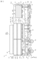
図1に示すように、半導体パッケージ10は、第1層L1を備えている。第1層L1の外形は、全体として略直方体状である。第1層L1は、第1主面10A及び第2主面10Bを有している。第1主面10Aは、第1層L1の外面のうち、最も面積の広い面の1つである。第1主面10Aに直交する方向を向いて視たとき、第1主面10Aは、長方形状である。第2主面10Bは、第1層L1の外面のうち、第1主面10Aとは反対側の面である。第2主面10Bは、第1主面10Aに平行である。第2主面10Bに直交する方向を向いて視たとき、第2主面10Bの形状は、第1主面10Aの形状と同じである。
<全体構成について>
図1に示すように、半導体パッケージ10は、第1層L1を備えている。第1層L1の外形は、全体として略直方体状である。第1層L1は、第1主面10A及び第2主面10Bを有している。第1主面10Aは、第1層L1の外面のうち、最も面積の広い面の1つである。第1主面10Aに直交する方向を向いて視たとき、第1主面10Aは、長方形状である。第2主面10Bは、第1層L1の外面のうち、第1主面10Aとは反対側の面である。第2主面10Bは、第1主面10Aに平行である。第2主面10Bに直交する方向を向いて視たとき、第2主面10Bの形状は、第1主面10Aの形状と同じである。
以下の説明では、第1主面10Aに直交する軸を第1軸Xとする。そして、第1軸Xに沿う方向のうちの特定の方向を第1正方向X1とし、第1正方向X1と反対方向を第1負方向X2とする。第1実施形態では、第1正方向X1は、第1主面10Aが向く方向と一致する。第1負方向X2は、第2主面10Bが向く方向と一致する。
半導体パッケージ10は、第1層L1に積層された第2層L2、第3層L3、第4層L4、及び第5層L5を備えている。第1軸Xに沿う方向を向いて透視したときに、第1層L1~第5層L5の各層の外形は、いずれも長方形状である。半導体パッケージ10の各層は、第1負方向X2側から第1正方向X1側に向かうに従って、第2層L2、第1層L1、第3層L3、第4層L4、及び第5層L5の順で並んでいる。
第1層L1は、第1封止部11と、複数の第1電子部品12と、複数の第1ビア配線14と、複数の第1部品外部端子15と、を有している。なお、第1層L1は、第1電子部品12を含む第1部品層である。
第1封止部11の外形は、略直方体状である。第1封止部11の外面のうちの第1正方向X1を向く平面は、第1主面10Aである。また、第1封止部11の外面のうちの第1負方向X2を向く平面は、第2主面10Bである。第1封止部11は、TEOS(Tetra EthOxy Silane)である。すなわち、第1封止部11は、無機材料を含んでいる。また、第1封止部11に適用される無機材料を含む材質としては、SiO2や、TiN、TiO、SiCOH等を採用可能である。
第1電子部品12は、受動部品又は能動部品である。受動部品は、インダクタ、抵抗、コンデンサのいずれかである。能動部品は、電流に対して増幅、整流、変換等の能動的な仕事を行う電子部品である。例えば、能動部品は、ダイオード、トランジスタ、及びこれらを含む集積回路等である。なお、当該集積回路が、インダクタ、抵抗、及びコンデンサを含んでいる場合でも、能動部品を1つでも有していれば、能動部品として扱う。以降の説明においても「電子部品」は、受動部品又は能動部品のいずれかを示す。
図1に示す例では、第1層L1は、3つの第1電子部品12を有している。3つの第1電子部品12は、2つの能動部品12A、及び1つの受動部品12Bである。すなわち、第1電子部品12のうちの少なくとも1つは、能動部品12Aである。また、第1電子部品12のうちの1つは、受動部品12Bである。
受動部品12Bは、無機材料を含んでいる。例えば、受動部品12Bがインダクタである場合、当該受動部品12Bは、無機材料として、Fe、FeSi系、及びクロム・ジルコニウム・タンタル合金等の材料を含んでいる。これらの材料は、インダクタのコアに含まれている。また、受動部品12Bがインダクタである場合、当該受動部品12Bは、無機材料として、Cu、Ag等の材料を含んでいる。これらの材料は、インダクタの配線に含まれている。
また、受動部品12Bがコンデンサである場合、当該受動部品12Bは、無機材料として、SiO2、SiN、チタン酸バリウム等の材料を含んでいる。これらの材料は、コンデンサのコアに含まれている。また、受動部品12Bがコンデンサである場合、当該受動部品12Bは、Al、Ni等の材料を含んでいる。これらの材料は、電極に含まれている。なお、受動部品12Bは、インダクタ及びコンデンサのどちらの場合においても、エポキシ系及びポリイミド系樹脂などを有機材料として含んでいる。
第1実施形態において、受動部品12Bにおける無機材料の体積分率は、80vol%以上である。すなわち、受動部品12Bにおける無機材料の体積分率は、50vol%以上である。
各第1電子部品12は、第1封止部11の内部に位置している。具体的には、3つの第1電子部品12は、それぞれ、第1主面10Aに平行な方向に並んでいる。また、各第1電子部品12は、それぞれ、第1層L1内部において、第2主面10B側に寄って位置している。具体的には、各第1電子部品12における一方の主面は、第1層L1の第2主面10Bと、概ね面一になっている。
第1電子部品12のうち、2つの能動部品12Aの第1主面10Aに直交する方向の最大寸法は同じである。また、残り1つの第1電子部品12である受動部品12Bの第1主面10Aに直交する方向の最大寸法は、各能動部品12Aの第1主面10Aに直交する方向の最大寸法より大きい。
各能動部品12Aは、部品本体12Mと、接続端子13と、内部側端子13Aと、を備えている。接続端子13は、第1電子部品12において当該第1電子部品12の外部の配線等と接続するための外部端子としての機能を有する。図1に示す例において、各能動部品12Aは、2つの接続端子13と、2つの内部側端子13Aとを有している。2つの接続端子13は、第1負方向X2側に向けて露出している。具体的には、各接続端子13は、部品本体12Mから突出している。また、各接続端子13は、第1封止部11における第2主面10B側において第1封止部11から露出している。なお、これら各接続端子13は、第1封止部11から突出している。
各第1電子部品12の接続端子13の外表面において、Cuの体積分率は、50vol%以上である。第1実施形態では、各接続端子13全体において、Cuの体積分率は、90vol%以上である。各接続端子13は、Cu成分の他に、S、Ni、及びO成分をわずかに含んでいる。
2つの内部側端子13Aは、部品本体12Mから第1正方向X1側に向けて露出している。すなわち、各内部側端子13Aは、第1主面10Aに直交する方向における接続端子13とは反対側で部品本体12Mから露出している。図1に示す例では、内部側端子13Aは、部品本体12Mから突出していない。換言すると、内部側端子13Aの第1正方向X1側の端面は、部品本体12Mと面一になっている。すなわち、接続端子13の突出量は、内部側端子13Aの突出量より大きい。各内部側端子13Aの材質は、接続端子13の材質と同じである。
図1に示す例において、第1電子部品12における受動部品12Bは、2つの接続端子13を有している。当該2つの接続端子13の材質は、能動部品12Aの接続端子13の材質と同じである。2つの接続端子13は、第1負方向X2側に向けて露出している。また、第1負方向X2側の各接続端子13は、第1封止部11における第2主面10B側において第1封止部11から露出している。なお、これら第1負方向X2側の各接続端子13は、第1封止部11から突出している。このように、各第1電子部品12の接続端子13は、第1封止部11における第2主面10Bにおいてのみ、第1封止部11から露出している。
図1に示す例において、第1層L1は、4つの第1ビア配線14を有している。各第1ビア配線14は、略円柱状である。各第1ビア配線14は、第1封止部11の内部で第1主面10Aに交差する方向に延びている。第1実施形態では、各第1ビア配線14は、第1主面10Aに直交する方向に延びている。各第1ビア配線14の第1端は、能動部品12Aにおける内部側端子13Aに接続している。また、各第1ビア配線14の第2端は、第1封止部11から露出している。すなわち、第1ビア配線14の端部は、第1主面10Aにおいて第1封止部11から露出している。
第1ビア配線14は、Cu成分を含んでいる。第1ビア配線14におけるCuの体積分率は、50vol%以上である。第1実施形態では、第1配線部22におけるCuの体積分率は、90vol%以上である。
複数の第1部品外部端子15は、第1封止部11から突出している。具体的には、複数の第1部品外部端子15は、第1封止部11の第1正方向X1側から露出している。各第1部品外部端子15は、第1ビア配線14の第2端に接続している。各第1部品外部端子15の材質は、第1ビア配線14の材質と同じである。
第2層L2は、第1層L1に対して第1負方向X2側に積層されている。換言すると、第2層L2は、第1層L1の第2主面10Bに、直接積層されている。したがって、第2層L2は、第1部品層に対して第1主面10Aに直交する方向に隣接している。
第2層L2は、第1絶縁樹脂部21と、第1配線部22と、複数の第1配線外部端子23と、を有している。したがって、第2層L2は、第1配線部22を含む第1配線層である。
第1絶縁樹脂部21の外形は、略直方体状である。第1絶縁樹脂部21の外形は、第2層L2の外形と略一致する。第1絶縁樹脂部21の材質は、無機フィラーを含む合成樹脂である。合成樹脂は、例えば、エポキシ系、及びポリイミド系の樹脂である。なお、第1絶縁樹脂部21は、第1封止部11から突出した第1電子部品12の接続端子13の周面を覆っている。
第1配線部22は、第1主面10Aに交差する方向に延びる複数の第1柱状配線22Bと、第1主面10Aに平行な方向に延びる複数の第1配線22Aと、を有している。第1柱状配線22Bは、第1配線22Aに接続している。これらの複数の第1柱状配線22B及び複数の第1配線22Aは、互いに接続している。なお、図1において一部の第1柱状配線22B及び一部の第1配線22Aにのみ符号を付している。
第1配線部22は、第1電子部品12における接続端子13に接続している。第1配線部22は、任意のパターンで、第1絶縁樹脂部21の内部で延びている。第1配線部22の材質は、第1ビア配線14の材質と同じである。すなわち、第1配線部22におけるCuの体積分率は、50vol%以上である。
複数の第1配線外部端子23は、第1絶縁樹脂部21から突出している。具体的には、複数の第1配線外部端子23は、第1絶縁樹脂部21の第1負方向X2側から露出している。各第1配線外部端子23の材質は、第1正方向X1側からCuを主成分とする層、Niを主成分とする層、及びAuを主成分とする層の3層構造になっている。なお、当該第1配線外部端子23は、半導体パッケージ10を基板等に実装する際の外部端子として機能する。なお、図1において一部の第1配線外部端子23にのみ符号を付している。
第3層L3は、第1層L1に対して第1正方向X1側に積層されている。換言すると、第3層L3は、第1層L1の第1主面10Aに積層されている。すなわち、第3層L3は、第1部品層に対して第1主面10Aに直交する方向に隣接している。
第3層L3は、第2絶縁樹脂部31と、第2配線部32と、複数の第2配線外部端子33と、を有している。第3層L3は、第2配線部32を含む第2配線層である。
第2絶縁樹脂部31の外形は、略直方体状である。第2絶縁樹脂部31の外形は、第3層L3の外形と略一致する。第2絶縁樹脂部31の材質は、無機フィラーを含む合成樹脂である。なお、第2絶縁樹脂部31は、第1部品外部端子15の周面を覆っている。
第2絶縁樹脂部31の外形は、略直方体状である。第2絶縁樹脂部31の外形は、第3層L3の外形と略一致する。第2絶縁樹脂部31の材質は、無機フィラーを含む合成樹脂である。なお、第2絶縁樹脂部31は、第1部品外部端子15の周面を覆っている。
第2配線部32は、第1主面10Aに平行な方向に延びる複数の第2配線32Aと、第1主面10Aに交差する方向に延びる複数の第2柱状配線32Bと、を有している。第2柱状配線32Bは、第2配線32Aに接続している。これらの複数の第2柱状配線32B及び複数の第2配線32Aは、互いに接続している。なお、図1において一部の第2柱状配線32B及び一部の第2配線32Aにのみ符号を付している。
第2配線部32は、第1部品外部端子15に接続している。すなわち、第2配線部32は、第1部品外部端子15を介して、第1層L1における第1ビア配線14に接続している。換言すると、第1ビア配線14の第2端は、第2配線層内の第2配線部32に接続している。
第2配線部32は、任意のパターンで、第2絶縁樹脂部31の内部で延びている。第2配線部32の材質は、第1配線部22の材質と同じである。すなわち、第2配線部32におけるCuの体積分率は、50vol%以上である。
複数の第2配線外部端子33は、第2絶縁樹脂部31から突出している。具体的には、複数の第2配線外部端子33は、第2絶縁樹脂部31の第1正方向X1側から露出している。各第2配線外部端子33の材質は、第1部品外部端子15の材質と同じである。
第4層L4は、第3層L3に対して第1正方向X1側に積層されている。第4層L4は、第2封止部41と、複数の第2電子部品42と、第2ビア配線44と、複数の第2部品外部端子45と、複数の接続部47と、アンダーフィル46と、を有している。なお、第4層L4は、第2電子部品42を含む第2部品層である。
第2封止部41の外形は、略直方体状である。第2封止部41の外形は、第4層L4の外形と略一致する。第2封止部41の材質は、無機フィラーを含む合成樹脂である。
図1に示す例では、第4層L4は、3つの第2電子部品42を備えている。第2電子部品42は、2つの能動部品42A、及び1つの受動部品42Bである。すなわち、第2電子部品42のうちの少なくとも1つは、能動部品42Aである。また、第2電子部品42のうちの1つは、受動部品42Bである。当該受動部品42Bにおける無機材料の体積分率は、80vol%以上である。
図1に示す例では、第4層L4は、3つの第2電子部品42を備えている。第2電子部品42は、2つの能動部品42A、及び1つの受動部品42Bである。すなわち、第2電子部品42のうちの少なくとも1つは、能動部品42Aである。また、第2電子部品42のうちの1つは、受動部品42Bである。当該受動部品42Bにおける無機材料の体積分率は、80vol%以上である。
各第2電子部品42は、第2封止部41の内部に位置している。具体的には、3つの第2電子部品42は、それぞれ、第1主面10Aに平行な方向に並んでいる。
各第2電子部品42は、接続端子43を備えている。接続端子43は、第2電子部品42において当該第2電子部品42の外部の配線等と接続するための外部端子としての機能を有する。
各第2電子部品42は、接続端子43を備えている。接続端子43は、第2電子部品42において当該第2電子部品42の外部の配線等と接続するための外部端子としての機能を有する。
図1に示す例において、各第2電子部品42は、2つの接続端子43を有している。各接続端子43は、第1負方向X2側に向けて露出している。これらの接続端子43は、第2絶縁樹脂部31に覆われていない。各第2電子部品42の接続端子43の材質は、第1電子部品12の接続端子43の材質と同じである。
第2ビア配線44は、略円柱状である。第2ビア配線44は、第2封止部41の内部で第1主面10Aに交差する方向に延びている。第1実施形態では、第2ビア配線44は、第1主面10Aに直交する方向に延びている。第2ビア配線44の第1端は、第2配線外部端子33のうちの1つに接続している。また、第2ビア配線44の第2端は、第2封止部41から露出している。すなわち、第2ビア配線44の端部は第1正方向X1側の面において、第2封止部41から露出している。第2ビア配線44の材質は、第1ビア配線14の材質と同じである。
複数の第2部品外部端子45は、第2封止部41から突出している。具体的には、複数の第2部品外部端子45は、第2封止部41の第1正方向X1側から露出している。第2部品外部端子45のうちの1つは、第2ビア配線44の第2端に接続している。各第2部品外部端子45の材質は、第1部品外部端子15の材質と同じである。
第2ビア配線44に接続していない第2配線外部端子33は、接続部47を介して第2電子部品42の接続端子43に接続している。接続部47は、はんだ等の導電性材料である。接続部47は、第2配線外部端子33の数に応じて存在する。各接続部47は、対応する第2配線外部端子33に塗布されている。すなわち、接続部47は、第2配線外部端子33第1正方向X1側の面を覆っている。
アンダーフィル46は、第2封止部41の内部に位置している。アンダーフィル46は、第2絶縁樹脂部31の第1正方向X1側から、接続端子43の第1正方向X1側の端までの領域に位置している。すなわち、アンダーフィル46は、第2配線外部端子33、接続部47、及び接続端子43の周面を覆っている。アンダーフィル46の材質は、例えば、エポキシ樹脂である。なお、アンダーフィル46の材質は、エポキシ系の樹脂に限らず、ポリイミド系の樹脂、液晶ポリマー系の樹脂、アクリル系の樹脂、フェノール系の樹脂、及びこれらの組み合わせでもよい。また、アンダーフィル46は、無機フィラーとして、シリカフィラーなどを含んでいてもよい。
第5層L5は、第4層L4に対して第1正方向X1側に積層されている。第5層L5は、第3絶縁樹脂部51と、第3配線部52と、を有している。第5層L5は、第3配線部52を含む第3配線層である。
第3絶縁樹脂部51の外形は、略直方体状である。第3絶縁樹脂部51の外形は、第5層L5の外形と略一致する。第3絶縁樹脂部51の材質は、第1絶縁樹脂部21の材質と同じである。なお、第3絶縁樹脂部51の第1負方向X2側に、第2部品外部端子45が食い込んでいる。
第3配線部52は、第1主面10Aに交差する方向に延びる複数の第3柱状配線52Bと、第1主面10Aに平行な方向に延びる複数の第3配線52Aと、を有している。第3柱状配線52Bは、第3配線52Aに接続している。なお、図1において一部の第3柱状配線52B及び一部の第3配線52Aにのみ符号を付している。
第3配線部52は、第2部品外部端子45に接続している。第3配線部52は、任意のパターンで、第3絶縁樹脂部51の内部で延びている。第3配線部52の材質は、第1配線部22の材質と同じである。すなわち、第3配線部52におけるCuの体積分率は、50vol%以上である。
<半導体パッケージの製造方法について>
半導体パッケージ10の製造方法について説明する。なお、図2~図11において、一部の部材にのみ符号を付している場合がある。
半導体パッケージ10の製造方法について説明する。なお、図2~図11において、一部の部材にのみ符号を付している場合がある。
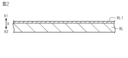
図2に示すように、まず、板状のベース基板BLを準備する。ベース基板BLの材質は、シリコンである。以下では、ベース基板BLの主面が第1軸Xに直交しているものとして説明する。第1負方向X2を向いて視たとき、ベース基板BLは、例えば、長方形状となっている。ベース基板BLの各辺の寸法は、半導体パッケージ10が複数個収容される寸法である。次に、ベース基板BLの第1正方向X1側、すなわち上面全体に第1リリース層RL1を塗布する。第1リリース層RL1は、例えば、赤外線硬化型樹脂製のテープ、アクリル樹脂系の接着剤、ポリイミド系の接着剤等の接着機能を有するシート状の部材である。
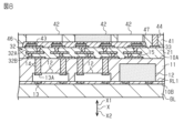
次に、図3に示すように、第1リリース層RL1上に、第1電子部品12を配置する。具体的には、第1電子部品12における接続端子13が、第1リリース層RL1と向かい合うようにして、第1電子部品12を配置する。
次に、図4に示すように、第1封止部11を形成する。具体的には、まず、各第1電子部品12及び第1リリース層RL1の第1正方向X1側から、CVD法等の公知の技術により、絶縁体を形成する。絶縁体の材質は、TEOSである。次に、当該絶縁体に対してボッシュ法等の公知の技術により、第1貫通孔PO1を形成する。第1貫通孔PO1は、第1負方向X2を視たときに、第1電子部品12の内部側端子13Aと重なる位置に形成される。
次に、図5に示すように、第1貫通孔PO1に対して第1ビア配線14を形成する。第1ビア配線14は、ビアフィル法などの公知の技術により形成される。なお、図示は省略するが、第1ビア配線14を形成する過程で、Cuからなるシード層が形成される。
次に、図6に示すように、第1封止部11に対して第1正方向X1側に第2絶縁樹脂部31、第2配線部32、及び第2配線外部端子33を形成する。第2絶縁樹脂部31は、フォトリソグラフィによって形成される。第2配線部32及び第2配線外部端子33は、セミアディティブ法などの公知の技術により形成される。なお、当該工程において、第2配線外部端子33に対して無電解めっき、又は電解めっき等の公知の方法で表面処理を施してもよい。
次に、図7に示すように、第2電子部品42を実装する。具体的には、第2配線外部端子33上に、第2電子部品42が有する端子をはんだで接続する。接続後のはんだは、接続部47となる。また、第2絶縁樹脂部31と、第2電子部品42との間にエポキシ樹脂を充填する。これにより、アンダーフィル46が形成される。
次に、第2封止部41を形成する。具体的には、第2電子部品42及び第2絶縁樹脂部31の第1正方向X1側から、絶縁体をラミネートする。絶縁体の材質は、無機フィラーを含む有機樹脂である。次に、当該絶縁体に対して第1正方向X1側からレーザーを照射する。具体的には、第2電子部品42に接続していない、第2配線外部端子33の第1正方向X1側の部分であって、第2ビア配線44を形成する部分の絶縁体にレーザーを照射する。これにより、絶縁体が加工され、第2貫通孔PO2が形成される。
次に、図8に示すように、第2貫通孔PO2に対して第2ビア配線44を形成する。第2ビア配線44は、ビアフィル法などの公知の技術により形成される。なお、図示は省略するが、第2ビア配線44を形成する過程で、Cuからなるシード層が形成される。そして、第2封止部41及び第2ビア配線44の第1正方向X1側の一部を研磨して所望のサイズとする。
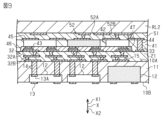
次に、図9に示すように、第3絶縁樹脂部51、第3配線部52、及び第2部品外部端子45を形成する。第3絶縁樹脂部51は、フォトリソグラフィによって形成される。第3配線部52及び第2部品外部端子45は、セミアディティブ法などの公知の技術により形成される。次に、第1リリース層RL1を切削により除去する。さらに、第3絶縁樹脂部51に対して第1正方向X1側に第2リリース層RL2を形成する。第2リリース層RL2は、第3絶縁樹脂部51の全体を覆うように形成される。第2リリース層RL2の材質は、第1リリース層RL1の材質と同じである。
次に、図10に示すように、第1封止部11に対して第1負方向X2側に第1絶縁樹脂部21、第1配線部22、及び第1配線外部端子23を形成する。第1絶縁樹脂部21は、フォトリソグラフィによって形成される。第1配線部22及び第1配線外部端子23の一部は、セミアディティブ法などの公知の技術により形成される。また、形成した第1配線外部端子23の一部に対して無電解めっき、又は電解めっき等の公知の方法でNiを主成分とする層と、Auを主成分とする層を形成する。これにより第1配線外部端子23が形成される。
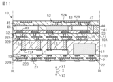
次に、図11に示すように、所望の半導体パッケージ10のサイズとなるように、破断線DLにてダイシングにより個片化する。そして、第2リリース層RL2を切削により除去する。
<第1実施形態の効果について>
(1-1)上記第1実施形態によれば、半導体パッケージ10は、能動部品12A及び受動部品12Bを有している。これら能動部品12A及び受動部品12Bは、半導体パッケージ10を形成する過程において実装される。すなわち、上記構成によれば、能動部品12A及び受動部品12Bは、予め良品と判定されたもののみを採用できる。そのため、半導体パッケージ10全体を形成した後に、これらの能動部品12A及び受動部品12Bに対して、正常に動作するか否かに関する試験を、必ずしも行う必要がない。このような構成によれば、半導体パッケージ10における良品率を高めることができる。
(1-1)上記第1実施形態によれば、半導体パッケージ10は、能動部品12A及び受動部品12Bを有している。これら能動部品12A及び受動部品12Bは、半導体パッケージ10を形成する過程において実装される。すなわち、上記構成によれば、能動部品12A及び受動部品12Bは、予め良品と判定されたもののみを採用できる。そのため、半導体パッケージ10全体を形成した後に、これらの能動部品12A及び受動部品12Bに対して、正常に動作するか否かに関する試験を、必ずしも行う必要がない。このような構成によれば、半導体パッケージ10における良品率を高めることができる。
(1-2)上記第1実施形態では、第1配線層である第2層L2は、第1部品層である第1層L1の第2主面10Bに積層されている。第2層L2が第1層L1に積層されることにより、第1層L1の第2主面10Bが第2層L2に覆われる。この構成によれば、第2層L2は、第1層L1に含まれる能動部品12A及び受動部品12Bに対して作用する外部からの衝撃を和らげることができる。
また、上記第1実施形態では、第2配線層である第3層L3は、第1部品層である第1層L1の第1主面10Aに積層されている。この構成によれば、能動部品12A及び受動部品12Bに対して、衝撃が作用することをさらに抑制できる。
(1-3)上記第1実施形態では、第1ビア配線14の第1端は第1電子部品12に接続している。また、第1ビア配線14の第2端は、第1配線層内の第1配線部22に接続している。すなわち、第1ビア配線14は、第1電子部品12と第1配線部22とを接続している。この構成によれば、第1ビア配線14により、第1電子部品12に対して、第1主面10Aに直交する方向から直接電流を流すことができる。換言すると、第1層L1内部において、第1主面10Aに平行に延びる配線及び第1主面10Aに交差する方向に延びるビア等の構成を必要とせず、第1電子部品12と第1配線部22とを接続できる。
(1-4)上記第1実施形態では、第1電子部品12の接続端子13の外表面におけるCuの体積分率は、50vol%以上である。また、第1配線部22におけるCuの体積分率は、50vol%以上である。上記第1実施形態において第1配線部22と接続端子13とを接続する第1ビア配線14の材質は、第1配線部22の材質と同じで、Cuを50vol%以上含んでいる。すなわち、接続端子13と第1ビア配線14との界面の材質が同様であることから、これら接続端子13と第1ビア配線14とが一体化しやすい。したがって、接続端子13と第1ビア配線14との接続強度を向上できる。同様に、第1配線部22と第1ビア配線14との界面の材質が同様であることから、第1配線部22と第1ビア配線14との接続強度を向上できる。したがって、第1電子部品12と第1配線部22との電気的接続が保たれやすい。
(1-5)上記第1実施形態において、受動部品12Bは、無機材料を含んでいる。当該受動部品12Bにおける無機材料の体積分率は、50vol%以上である。また、受動部品12Bの周面を覆う第1封止部11は、無機材料を含んでいる。すなわち、この構成によれば、受動部品12Bの熱膨張係数と第1封止部11の熱膨張係数との差が極端に異なるといったことはない。このような熱膨張係数の関係であれば、温度変化に伴うこれらの部材の変形量が大きく乖離しないので、熱変形に伴う第1層L1における反りを抑制できる。
(1-6)上記第1実施形態において、受動部品12Bの第1主面10Aに直交する方向の最大寸法は、能動部品12Aの第1主面10Aに直交する方向の最大寸法より大きい。すなわち、受動部品12Bの厚さ寸法は相応に大きい。そのため、例えば、受動部品12Bをインダクタとした場合、所望のインダクタンスを得るような設計が実現しやすい。また、受動部品12Bがコンデンサである場合も、所望のキャパシタンスを得るような設計が実現しやすい。
(1-7)上記第1実施形態では、第1電子部品12の能動部品12Aにおける接続端子13の突出量は、内部側端子13Aの突出量よりも大きくなっている。接続端子13の突出量が大きいことにより、半導体パッケージ10の製造工程において、能動部品12Aを配置する際の位置決めとして接続端子13を利用可能である。また、接続端子13により、第1層L1の第1負方向X2を向く面の表面積が大きくなるため、第2層L2との密着性が向上する。また、内部側端子13Aの突出量が比較的に小さいことにより、能動部品12A自体の第1主面10Aに直交する方向の寸法が大きくなることを抑制できる。
(第2実施形態)
<全体構成について>
以下、半導体パッケージの第2実施形態について説明する。
<全体構成について>
以下、半導体パッケージの第2実施形態について説明する。
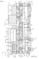
図12に示すように、第2実施形態の半導体パッケージ10は、第1層L1及び第2層L2を備えている。第1層L1は、第1主面10A及び第2主面10Bを有している。第1主面10A及び第2主面10Bについては、第1実施形態と同様である。また、第1軸X、第1正方向X1、第1負方向X2についても第1実施形態と同様の扱いとする。
第1層L1は、第1部品層PT1と、2つの第1配線層LN1を備えている。第2実施形態では、第1部品層PT1とは別の層である各第1配線層LN1が、第1部品層PT1の内部に埋まっているような状態になっている。
第1部品層PT1は、第1封止部21と、複数の第1電子部品22と、複数の第1ビア配線24と、複数の第1部品外部端子25と、を有している。
第1封止部21の外形は、略直方体状である。上述の2つの第1配線層LN1は、第1封止部21の内部に位置している。すなわち、第1配線層LN1は、第1部品層PT1の一部分である第1封止部21又は第1電子部品22に対して第1主面10Aに直交する方向に隣接している。第1封止部21の材質は、第1実施形態と同じである。すなわち、第1封止部21は、無機材料を含んでいる。
第1封止部21の外形は、略直方体状である。上述の2つの第1配線層LN1は、第1封止部21の内部に位置している。すなわち、第1配線層LN1は、第1部品層PT1の一部分である第1封止部21又は第1電子部品22に対して第1主面10Aに直交する方向に隣接している。第1封止部21の材質は、第1実施形態と同じである。すなわち、第1封止部21は、無機材料を含んでいる。
図12に示す例では、第1層L1は、3つの第1電子部品22を有している。3つの第1電子部品22は、すべて能動部品である。すなわち、第1電子部品22のうちの少なくとも1つは、能動部品である。
各第1電子部品22は、第1封止部21の内部に位置している。具体的には、3つの第1電子部品22は、それぞれ、第1主面10Aに平行な方向に並んでいる。また、各第1電子部品22は、それぞれ、第1層L1内部において、第2主面10B側に寄って位置している。具体的には、各第1電子部品22における一方の主面は、第1層L1の第2主面10Bと、概ね面一になっている。
3つの第1電子部品22のうちの2つは、それぞれ別の第1配線層LN1に隣接している。具体的には、2つの第1電子部品22における第1正方向X1側の面には、それぞれ第1配線層LN1が積層されている。なお、各第1配線層LN1は、第1層L1内においては互いに電気的に接続していない。
各第1電子部品22は、接続端子26を備えている。接続端子26は、第1電子部品22において当該第1電子部品22の外部の配線等と接続するための外部端子としての機能を有する。図12に示す例において、各第1電子部品22は、複数の接続端子26を有している。各接続端子26は、第1負方向X2側に向けて露出している。また、各接続端子26は、第1封止部21における第2主面10B側において第1封止部21から露出している。なお、各接続端子26は、第1封止部21から突出している。各接続端子26の外表面において、Cuの体積分率は、50vol%以上である。なお、第2実施形態における接続端子26の材質は、第1実施形態と同様である。
各第1配線層LN1は、第1配線部12と第1絶縁樹脂部11とを有している。なお、図12では、第1配線層LN1内部の第1配線部12及び第1絶縁樹脂部11の図示を省略している。第1配線部12及び第1絶縁樹脂部11については、第1実施形態と同様の構成である。すなわち、各第1絶縁樹脂部11の外形は、略直方体状である。ただし、各第1絶縁樹脂部11における第1主面10Aに平行な方向の寸法は、第1層L1における第1主面10Aに平行な方向の寸法よりも小さい。また、各第1絶縁樹脂部11における第1主面10Aに直交する方向の寸法は、第1層L1における第1主面10Aに直交する方向の寸法よりも小さい。各第1絶縁樹脂部11の材質は、無機フィラーを含む合成樹脂である。
各第1配線部12は、任意のパターンで、各第1絶縁樹脂部11の内部で延びている。各第1配線部12の材質は、第1実施形態の第1配線部12の材質と同じである。すなわち、第1配線部12におけるCuの体積分率は、50vol%以上である。
第1配線層LN1に隣接する2つの第1電子部品22は、貫通配線23を備えている。すなわち、能動部品から選ばれる1以上は、貫通配線23を備えている。当該能動部品は、それぞれ、2つの貫通配線23を備えている。各貫通配線23は、略円柱状である。各貫通配線23は、当該能動部品を第1主面10Aに直交する方向に貫通している。各貫通配線23における第1正方向X1側の端は、第1配線層LN1の第1配線部12に接続している。また、各貫通配線23における第1負方向X2側の端は、接続端子26に接続している。
図12に示す断面上では、第1部品層PT1は、4つの第1ビア配線24を有している。各第1ビア配線24は、略円柱状である。各第1ビア配線24における径は、各貫通配線23における径よりも大きい。換言すると、貫通配線23の第1主面10Aに平行な方向の最大寸法は、第1ビア配線24の第1主面10Aに平行な方向の最大寸法よりも小さい。各第1ビア配線24は、第1封止部21の内部で第1主面10Aに交差する方向に延びている。第2実施形態では、各第1ビア配線24は、第1主面10Aに直交する方向に延びている。
4つの第1ビア配線24のうちの2つは、第1配線層LN1から延びている。すなわち、当該第1ビア配線24の第1負方向X2側の第1端は、第1配線層LN1の第1配線部12に接続している。また、当該第1ビア配線24の第1正方向X1側の第2端は、第1主面10A側において第1封止部21から露出している。
また、残りの2つの第1ビア配線24における第1負方向X2側の第1端は、第2主面10B側において、第1封止部21から露出している。また、当該2つの第1ビア配線24における第1正方向X1側の第2端は、第1主面10A側において第1封止部21から露出している。すなわち、第2実施形態における4つの第1ビア配線24の端部は、第1主面10A側において、第1封止部21から露出している。
第1ビア配線24は、Cu成分を含んでいる。第1ビア配線24におけるCuの体積分率は、50vol%以上である。第2実施形態では、第1実施形態と同様に、第1ビア配線24におけるCuの体積分率は、90vol%以上である。
図12に示す断面上では、第1層L1は、10個の第1部品外部端子25を有している。なお、第1層L1は、図12の断面で図示されていないその他の第1部品外部端子25を有していることもある。このうちの2つの第1部品外部端子25は、第1封止部21の第1負方向X2側から突出している。当該第1部品外部端子25は、それぞれ、第2主面10B側において第1封止部21から露出する第1ビア配線24の第1端に接続している。これらの10個の第1部品外部端子25の材質は、接続端子26の材質と同じである。
また、図12に示す断面上の第1部品外部端子25のうちの残りの8つの第1部品外部端子25は、第1封止部21の第1正方向X1側において露出している。当該8つの第1部品外部端子25の周面は、第1封止部21に覆われている。また、このうちの4つの第1部品外部端子25は、第1ビア配線24の第1正方向X1側の端に接続している。残りの4つの第1部品外部端子25は、第1配線層LN1に対して第1正方向X1側に直接積層されている。当該第1部品外部端子25は、第1配線層LN1における第1配線部12と電気的に接続している。これら8つの第1部品外部端子25の材質は、第1配線部12の材質と同じである。なお、図12において、一部の第1部品外部端子25にのみ符号を付している。
第2層L2は、第1層L1の第1正方向X1側に直接積層されている。第2層L2は、第2部品層PT2と4つの第2配線層LN2と、を備えている。上述の第1層L1と同様に、第2層L2においても、第2部品層PT2とは別の層である第2配線層LN2が、第2部品層PT2の内部に埋まっているような状態になっている。
第2部品層PT2は、第2封止部41と、複数の第2電子部品42と、複数の第2部品外部端子43と、を有している。
第2封止部41の外形は、略直方体状である。上述の4つの第2配線層LN2は、第2封止部41の内部に位置している。すなわち、第2配線層LN2は、第2部品層PT2の一部である第2封止部41又は第2電子部品42に対して第1主面10Aに直交する方向に隣接している。第2封止部41の材質は、第1封止部21の材質と同じである。すなわち、第2封止部41は、無機材料を含んでいる。
第2封止部41の外形は、略直方体状である。上述の4つの第2配線層LN2は、第2封止部41の内部に位置している。すなわち、第2配線層LN2は、第2部品層PT2の一部である第2封止部41又は第2電子部品42に対して第1主面10Aに直交する方向に隣接している。第2封止部41の材質は、第1封止部21の材質と同じである。すなわち、第2封止部41は、無機材料を含んでいる。
図12に示す例では、第2層L2は、5つの第2電子部品42を有している。5つの第2電子部品42のうちの4つは、能動部品42Aである。残りの1つの第2電子部品42は、受動部品42Bである。すなわち、第2電子部品42のうちの少なくとも1つは、能動部品42Aである。第2電子部品42のうちの少なくとも1つは、受動部品42Bである。
4つの能動部品42Aのうちの2つは、第1主面10Aに平行な方向に並んでいる。そして、これら2つの能動部品42Aの第1負方向X2側の面には、それぞれ第2配線層LN2が積層されている。さらに、2つの能動部品42Aの第1正方向X1側の面には、第2配線層LN2及び別の能動部品42Aが積層されている。したがって、これらは、第1正方向X1側に向かって、第2配線層LN2、能動部品42A、第2配線層LN2、及び能動部品42Aの順に積層された合計4つの要素からなる積層物となっている。そして、当該積層物が、第1主面10Aに平行な方向に2組並んでいる。また、隣接する第2配線層LN2と能動部品42Aとは、互いに電気的に接続している。なお、各第2配線層LN2は、第2層L2内においては互いに電気的に接続していない。
ここで、第1軸Xに沿う方向に積層された1組の積層物における2つの能動部品42Aを、それぞれ、第1能動部品42A1及び第2能動部品42A2と呼称する。第1能動部品42A1は、第2能動部品42A2に対して第1負方向X2側に位置している。第1能動部品42A1と第2能動部品42A2とは、第1主面10Aに直交する方向において、第1部品層PT1に対して積層されている。また、第1能動部品42A1と第1部品層PT1との間には、電子部品は存在しない。すなわち、第1能動部品42A1及び第2能動部品42A2は、間に他の電子部品を介することなく第1主面10Aに直交する方向において、第1部品層PT1に対して積層されている。第1主面10Aに直交する方向における第1能動部品42A1の最大寸法は、第1主面10Aに直交する方向における第2能動部品42A2の最大寸法と同じである。各能動部品42Aの厚さ寸法は同じである。
第2電子部品42における受動部品42Bは、能動部品42A及び第2配線層LN2が積層された2組の積層物に対して、第1主面10Aに平行な方向において並んで位置している。受動部品42Bは、無機材料を含んでいる。当該受動部品42Bにおける無機材料の体積分率は、80vol%以上である。
受動部品42Bの第1主面10Aに直交する方向の最大寸法は、第1能動部品42A1の第1主面10Aに直交する方向の最大寸法と第2能動部品42A2の第1主面10Aに直交する方向の最大寸法を合計した値より大きくなっている。
上述した各第2配線層LN2は、第2配線部32と第2絶縁樹脂部31とを有している。なお、図12では、第2配線層LN2内部の第2配線部32及び第2絶縁樹脂部31の図示を省略している。第2配線部32及び第2絶縁樹脂部31については、上記第1配線層LN1と同様の構成である。すなわち、各第2絶縁樹脂部31の外形は、略直方体状である。ただし、第2配線層LN2が第2部品層PT2内に埋まったような状態になっていることから、各第2絶縁樹脂部31における第1主面10Aに平行な方向の寸法は、第2層L2における第1主面10Aに平行な方向の寸法よりも小さい。また、各第2絶縁樹脂部31における第1主面10Aに直交する方向の寸法は、第2層L2における第1主面10Aに直交する方向の寸法よりも小さい。各第2絶縁樹脂部31の材質は、無機フィラーを含む合成樹脂である。
各第2配線部32は、任意のパターンで、各第2絶縁樹脂部31の内部で延びている。各第2配線部32の材質は、第2配線部32の材質と同じである。すなわち、第2配線部32におけるCuの体積分率は、50vol%以上である。
図12に示す断面上では、第2層L2は、8つの第2部品外部端子43を有している。なお、第2層L2は、図12の断面で図示されていないその他の第2部品外部端子43を有していることもある。図12に示す断面上の第2部品外部端子43のうちの7つの第2部品外部端子43は、第2配線層LN2に対して第1負方向X2側に直接積層されている。これら7つの第2部品外部端子43は、第2配線層LN2に対して電気的に接続している。また、図12に示す断面上の第2部品外部端子43のうちの残りの1つの第2部品外部端子43は、第2電子部品42の受動部品42Bの第1負方向X2側に直接積層されている。
図12に示す断面上の8つの第2部品外部端子43の周面は、第2封止部41に覆われている。また、8つの第2部品外部端子43は、第2封止部41の第1負方向X2側において露出している。すなわち、各第2部品外部端子43は、第2封止部41における第1部品層PT1側の面から露出している。
また、上述したように、図12に示す断面上における第1部品外部端子25のうちの8つは、第1封止部21の第1正方向X1側において露出している。すなわち、第1部品外部端子25は、第1封止部21における第2部品層PT2側の面から露出している。第1部品外部端子25は、間に他の部材を介することなく、第2部品外部端子43に接続している。また、同様に、第1正方向X1を向く第1封止部21は、間に他の部材を介することなく、第1負方向X2を向く第2封止部41に接触している。
第1層L1及び第2層L2が有する各部材は、無機材料を含んでいる。第2実施形態において、半導体パッケージ10全体において、ほとんどが無機材料である。具体的には、半導体パッケージ10全体での無機材料の体積分率は、90vol%以上である。
<第2実施形態の効果>
(2-1)上記第2実施形態によれば、第1部品層PT1は、第1電子部品22を有している。第1電子部品22は、半導体パッケージ10を形成する過程において実装される。すなわち、上記構成によれば、第1電子部品22は、予め良品と判定されたもののみを採用できる。そのため、半導体パッケージ10全体を形成した後に、これらの第1電子部品22に対して、正常に動作するか否かに関する試験を、必ずしも行う必要がない。このような構成によれば、半導体パッケージ10における良品率を高めることができる。
(2-1)上記第2実施形態によれば、第1部品層PT1は、第1電子部品22を有している。第1電子部品22は、半導体パッケージ10を形成する過程において実装される。すなわち、上記構成によれば、第1電子部品22は、予め良品と判定されたもののみを採用できる。そのため、半導体パッケージ10全体を形成した後に、これらの第1電子部品22に対して、正常に動作するか否かに関する試験を、必ずしも行う必要がない。このような構成によれば、半導体パッケージ10における良品率を高めることができる。
(2-2)第2実施形態において、第1電子部品22から選ばれる1以上は、貫通配線23を備えている。貫通配線23は、第1配線部12に接続している。この構成によれば、貫通配線23により、第1電子部品22内部において第1主面10Aに直交する方向に電流を流すことができる。すなわち、この構成によれば、第1電子部品22を介して第1配線部12に電流を流すことができるため、第1電子部品22を避けて配線パターンを設計する必要がなく、配線パターンが複雑になることを抑制できる。
(2-3)第2実施形態において、各貫通配線23の第1主面10Aに平行な方向の最大寸法は、各第1ビア配線24の第1主面10Aに平行な方向の最大寸法よりも小さい。この構成によれば、第1ビア配線24には貫通配線23よりも大きな電流を流すことができる。すなわち、第1ビア配線24における第1主面10Aに平行な方向の最大寸法と貫通配線23における第1主面10Aに平行な方向の最大寸法とが同じ場合と比較して、第1部品層PT1に対して大きな電流を付与できる。
(2-4)第2実施形態において、受動部品42Bにおける無機材料の体積分率は、80vol%以上である。また、半導体パッケージ10全体での無機材料の体積分率は、90vol%以上である。この構成によれば、半導体パッケージ10全体において、熱膨張係数の均一化が図れる。そのため、半導体パッケージ10において、局所的な熱変形が生じることを抑制できる。
(2-5)第2実施形態において、第1部品外部端子25は、間に他の部材を介することなく、第2部品外部端子43に接続している。つまり、第2部品層PT2は、ビア等の他の配線を介さずに第1部品層PT1に接続している。そのため、第1部品層PT1から第2部品層PT2に電流を流したときに、これらの部材の界面で直流抵抗が大きくなることを抑制できる。
(2-6)第2実施形態において、受動部品42Bの第1主面10Aに直交する方向の最大寸法は、第1能動部品42A1の第1主面10Aに直交する方向の最大寸法と第2能動部品42A2の第1主面10Aに直交する方向の最大寸法を合計した値より大きい。この構成によれば、例えば、受動部品42Bがインダクタである場合、コアの容量を確保できる。そのため、取得できるインダクタンスを大きくできる。なお、この構成によれば、受動部品としてコンデンサを採用した場合も、キャパシタンスを大きくし得る。
<変更例>
上記第1実施形態及び第2実施形態は、以下のように変更して実施することができる。上記第1実施形態、第2実施形態、及び以下の変更例は、技術的に矛盾しない範囲で組み合わせて実施することができる。なお、以下図13~図15に示す変更例では、第1実施形態及び第2実施形態と同様の構成を有する箇所について、説明を省略又は簡略化することがある。なお、図13~図15において第1実施形態及び第2実施形態と同様の構成の箇所については、符号の一部を省略して図示している場合がある。
上記第1実施形態及び第2実施形態は、以下のように変更して実施することができる。上記第1実施形態、第2実施形態、及び以下の変更例は、技術的に矛盾しない範囲で組み合わせて実施することができる。なお、以下図13~図15に示す変更例では、第1実施形態及び第2実施形態と同様の構成を有する箇所について、説明を省略又は簡略化することがある。なお、図13~図15において第1実施形態及び第2実施形態と同様の構成の箇所については、符号の一部を省略して図示している場合がある。
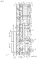
・第2実施形態において、さらに、第1部品層PT1に対して配線層が積層されていてもよい。例えば、図13に示す例では、半導体パッケージ10は、第3層L3を備えている。第3層L3は、第1層L1に対して第1負方向X2側に積層されている。換言すると、第3層L3は、第1層L1の第2主面10Bに、直接積層されている。したがって、第3層L3は、第1部品層PT1に対して第1主面10Aに直交する方向に隣接している。
第3層L3は、第3絶縁樹脂部51と、第3配線部52と、複数の第3配線外部端子53と、を有している。したがって、第3層L3は、第3配線部52を含む第3配線層LN3である。なお、第3配線層LN3は、第1実施形態の第2配線層と同様の構成である。
第3絶縁樹脂部51の外形は、略直方体状である。第3絶縁樹脂部51の材質は、有機樹脂のみである。なお、第3絶縁樹脂部51は、第1封止部21から突出した第1部品外部端子25、及び接続端子26の周面を覆っている。
第3配線部52は、第1部品外部端子25または接続端子26に接続している。第3配線部52は、任意のパターンで、第3絶縁樹脂部51の内部で延びている。第3配線部52の材質は、第1配線部12の材質と同じである。すなわち、第3配線部52におけるCuの体積分率は、50vol%以上である。
複数の第3配線外部端子53は、第3絶縁樹脂部51から突出している。具体的には、複数の第3配線外部端子53は、第3絶縁樹脂部51の第1負方向X2側から露出している。各第3配線外部端子53の材質は、第1正方向X1側からCuを主成分とする層、Niを主成分とする層、及びAuを主成分とする層の3層構造になっている。
仮に、第3絶縁樹脂部51が無機材料のみで構成されている場合、半導体パッケージ10の製造環境において、高いクリーン度が求められる。図13に示す例では、第3絶縁樹脂部51の材質は、有機樹脂のみである。したがって、図13に示す例では、第3絶縁樹脂部51が無機材料のみで構成される場合と比較して、製造環境におけるクリーン度の高さがそれほど求められず、製造にかかるコストが大きくなることを抑制できる。なお、第3絶縁樹脂部51が有機樹脂のみで構成される場合に限らず、無機フィラーを含む有機樹脂であっても同様の効果を奏する。
・第2実施形態において、半導体パッケージ10は、さらに、マザー基板に接続するための部材を備えていてもよい。図13に示す例では、半導体パッケージ10は、ランド部54を備えている。ランド部54は、はんだ等の導電性材料である。ランド部54は、一部の第3配線外部端子53に塗布されている。ランド部54は、当該第3配線外部端子53の第1負方向X2側の面を覆っている。すなわち、ランド部54は、第3配線層LN3の第1主面10Aに直交する方向において、第1部品層PT1と反対側を向く面に位置する第3配線外部端子53上に位置している。ランド部54は、第3配線層LN3に実装されるマザー基板を接続するための部材である。
この構成によれば、ランド部54の存在により、第3配線部52の配線パターンを任意のパターンに設計できる。換言すると、第3配線部52の配線パターンは、マザー基板と第1部品層PT1における第1電子部品22との接続を鑑みて好適なパターンに設計可能である。
・第2実施形態において、第1部品層PT1に積層される能動部品42Aの大きさは、全て同じでなくてもよい。図13に示す例において、第2部品層PT2が有する能動部品42Aのうち、最も第1正方向X1側に位置する2つの能動部品42Aの第1正方向X1の面は、第2封止部41から露出している。ここで、図13に示す例における当該2つの能動部品42Aを、それぞれ、第1能動部品42A1、第2能動部品42A2と呼称する。第1能動部品42A1及び第2能動部品42A2は、第1主面10Aに直交する方向において第1部品層PT1に対して積層されている。なお、図13に示す例では、第1能動部品42A1及び第2能動部品42A2は、第2配線層LN2及び他の能動部品42Aを介して第1部品層PT1に積層されている。第1能動部品42A1及び第2能動部品42A2は、第1主面10Aに平行な方向において、他の電子部品を介することなく並んでいる。
また、図13に示す例において、半導体パッケージ10は、第3能動部品42A3と、第4配線層LN4と、を備えている。第4配線層LN4の構成は、第2実施形態の第2配線層LN2の構成と同様である。すなわち、第4配線層LN4は、第4絶縁樹脂部61と、第4配線部62とを有している。第4配線部62は、第4絶縁樹脂部61の内部で任意のパターンで延びている。
図13に示す例では、第4配線層LN4及び第3能動部品42A3は、第1主面10Aに直交する方向において第1部品層PT1に対して積層されている。具体的には、第3能動部品42A3は、第1主面10Aに直交する方向において、第4配線層LN4を介して第1能動部品42A1及び第2能動部品42A2に対して積層されている。なお、第3能動部品42A3と、第1能動部品42A1及び第2能動部品42A2との間に他の電子部品は介されていない。第1主面10Aに直交する方向から透視したとき、第3能動部品42A3及び第4配線層LN4は、第1能動部品42A1及び第2能動部品42A2に重なっている。この構成によれば、第1能動部品42A1及び第2能動部品42A2を介して、第3能動部品42A3に電力が供給される。すなわち、半導体パッケージ10は、高集積化した能動部品42Aを含んでいる。
・第2実施形態において、第1部品層PT1に対して第1正方向X1に配線層が積層されていてもよい。また、第1部品層PT1に対して複数の配線層が積層されていてもよい。
図14に示す例では、第2実施形態における第2層L2は、第2配線層LN2のみで構成されている。また、図14に示す例では、半導体パッケージ10は、第2層L2に対して第1正方向X1に積層される第4層L4を備えている。第4層L4は、第4配線層LN4のみで構成されている。なお、図14に示す例において、半導体パッケージ10は、図13に示す例と同様の第3配線層LN3を備えている。
第2配線層LN2は、第2絶縁樹脂部31と、第2配線部32と、複数の第2配線外部端子33と、を有している。
第2絶縁樹脂部31の外形は、略直方体状である。第2絶縁樹脂部31の材質は、無機フィラーを含む有機樹脂である。第2配線部32は、第1主面10Aに交差する方向に延びる複数の第2柱状配線32Bと、第1主面10Aに平行な方向に延びる複数の第2配線32Aと、を有している。各第2配線32Aは、各第2柱状配線32Bに接続している。各第2柱状配線32Bは、略円錐台状である。各第2柱状配線32Bは、第1正方向X1に向かうほど、径が小さくなっている。すなわち、各第2柱状配線32Bは、第4配線層LN4に向かうほど、第1主面10Aに平行な方向の最大寸法が小さくなっている。
第2絶縁樹脂部31の外形は、略直方体状である。第2絶縁樹脂部31の材質は、無機フィラーを含む有機樹脂である。第2配線部32は、第1主面10Aに交差する方向に延びる複数の第2柱状配線32Bと、第1主面10Aに平行な方向に延びる複数の第2配線32Aと、を有している。各第2配線32Aは、各第2柱状配線32Bに接続している。各第2柱状配線32Bは、略円錐台状である。各第2柱状配線32Bは、第1正方向X1に向かうほど、径が小さくなっている。すなわち、各第2柱状配線32Bは、第4配線層LN4に向かうほど、第1主面10Aに平行な方向の最大寸法が小さくなっている。
第2配線部32は、任意のパターンで、第2絶縁樹脂部31の内部で延びている。第2配線部32の材質は、第1配線部12の材質と同じである。すなわち、第2配線部32におけるCuの体積分率は、50vol%以上である。
図14に示す断面上では、第2配線層LN2は、21個の第2配線外部端子33を有している。各第2配線外部端子33の材質は、第2配線部32の材質と同じである。このうちの10個の第2配線外部端子33は、第2配線部32に対して第1負方向X2側に位置している。当該10個の第2配線外部端子33の周面は、第2絶縁樹脂部31に覆われている。当該10個の第2配線外部端子33は、第2絶縁樹脂部31の第1負方向X2側において露出している。これら10個の第2配線外部端子33は、間に他の部材を介することなく、第1部品外部端子25に接続している。
残りの11個の第2配線外部端子33は、第2配線部32に対して第1正方向X1側に位置している。当該11個の第2配線外部端子33は、第2絶縁樹脂部31の第1負方向X2側において露出している。具体的には、当該11個の第2配線外部端子33は、第2絶縁樹脂部31に対して第1正方向X1に突出している。すなわち、第2配線外部端子33は、第2絶縁樹脂部31における第4配線層LN4側の面から突出している。これら11個の第2配線外部端子33の周面は他の部材に覆われていない。
図14に示す例では、上述したように第4層L4は、第4配線層LN4のみで構成されている。第4配線層LN4は、第4絶縁樹脂部61と、第4配線部62と、複数の第4配線外部端子63と、を有している。
第4絶縁樹脂部61の外形は、略直方体状である。第4絶縁樹脂部61の材質は、無機フィラーを含む有機樹脂である。第4配線部62は、第1主面10Aに交差する方向に延びる複数の第4柱状配線62Bと、第1主面10Aに平行な方向に延びる複数の第4配線62Aと、を有している。各第4配線62Aは、各第4柱状配線62Bに接続している。各第4柱状配線62Bは、略円錐台状である。各第4柱状配線62Bは、第1負方向X2に向かうほど、径が小さくなっている。すなわち、各第4柱状配線62Bは、第2配線層LN2に向かうほど、第1主面10Aに平行な方向の最大寸法が小さくなっている。
図14に示す断面上では、第4配線層LN4は、20個の第4配線外部端子63を有している。各第4配線外部端子63の材質は、第4配線部62の材質と同じである。このうちの9個の第4配線外部端子63は、第4配線部62に対して第1正方向X1側に位置している。当該9個の第4配線外部端子63の周面は、第2絶縁樹脂部31に覆われている。当該9個の第4配線外部端子63は、第4絶縁樹脂部61の第1正方向X1側において露出している。
残りの11個の第4配線外部端子63は、第4配線部62に対して第1負方向X2側に位置している。当該11個の第4配線外部端子63は、第2絶縁樹脂部31の第1負方向X2側において露出している。具体的には、当該11個の第4配線外部端子63は、第4絶縁樹脂部61に対して第1負方向X2に突出している。すなわち、第4配線外部端子63は、第4絶縁樹脂部61における第2配線層LN2側の面から突出している。これら11個の第4配線外部端子63の周面は他の部材に覆われていない。当該第4配線外部端子63は、第2配線外部端子33に接続している。当該第4配線外部端子63及び第2配線外部端子33の周面は、他の部材に覆われていない。したがって、第2絶縁樹脂部31と第4絶縁樹脂部61との間に空隙が生じている。
図14に示す例では、第2絶縁樹脂部31と第4絶縁樹脂部61との間に空隙が生じている。この構成によれば、半導体パッケージ10全体に対して曲げ応力が発生した場合でも、当該空隙により、応力を分散できる。すなわち、この構成によれば、半導体パッケージ10に対して発生した曲げ応力によって半導体パッケージ10にクラック等が発生することを抑制できる。
また、図14に示す例では、各第2柱状配線32Bは、第4配線層LN4に向かうほど、第1主面10Aに平行な方向の最大寸法が小さくなっている。また、各第4柱状配線62Bは、第2配線層LN2に向かうほど、第1主面10Aに平行な方向の最大寸法が小さくなっている。すなわち、第2柱状配線32Bと第4柱状配線62Bとの形状は第1軸Xに沿う方向に反転している。第2配線層LN2と第4配線層LN4とを同様の工程で製造した場合、第2柱状配線32B及び第4柱状配線62Bは、同様のテーパ形状になる。一方で、第2配線層LN2と第4配線層LN4とを形成した後に、互いに積層した場合、各柱状配線の形状が第2配線層LN2と第4配線層LN4とで反転できる。上記構成によれば、各配線層をそれぞれ並行して形成することも可能である。すなわち、各配線層を並行して形成することで、製造時間の短縮を図ることもできる。
・第2実施形態において、第2部品層PT2は、隣接する層の全体を覆っていなくてもよい。図14に示す例では、半導体パッケージ10は、第4層L4の第1正方向X1側に積層される第5層L5を備えている。第5層L5は、第1部分P1と第2部分P2とを有している。
第1部分P1は、第2部品層PT2と、4つの第5配線層LN5と、ダミー部DMと、を備えている。第1部分P1においても、第2部品層PT2とは別の層である第5配線層LN5が、第2部品層PT2の内部に埋まっているような状態になっている。
第2部品層PT2は、第2封止部41と、複数の第2電子部品42と、を有している。第2封止部41の外形は、略直方体状である。上述の4つの第5配線層LN5は、第2封止部41の内部に位置している。すなわち、第5配線層LN5は、第2部品層PT2の一部である第2封止部41又は第2電子部品42に対して第1主面10Aに直交する方向に隣接している。第2封止部41の材質は、無機フィラーを含む合成樹脂である。図14に示す例では、無機フィラーは、シリカである。すなわち、第2封止部41は、無機材料を含んでいる。
図14に示す例では、第2部品層PT2は、4つの第2電子部品42を有している。第2電子部品42は、全て能動部品42Aである。各能動部品42Aは、第2封止部41の内部に位置している。
4つの第2電子部品42のうちの2つは、第1主面10Aに平行な方向に並んでいる。そして、これら2つの第2電子部品42の第1負方向X2側の面には、それぞれ第5配線層LN5が積層されている。さらに、一方の能動部品42Aの第1正方向X1側の面には、第5配線層LN5、別の第2電子部品42、第5配線層LN5、及び別の第2電子部品42がこの順で積層された合計6つの要素からなる積層物となっている。当該積層物において、隣接する第5配線層LN5と第2電子部品42とは、互いに電気的に接続している。なお、各第5配線層LN5は、第1部分P1内においては互いに電気的に接続していない。
この積層物に含まれる3つの第2電子部品42のうちの2つは、4つの貫通配線44を備えている。具体的には、積層された3つの第2電子部品42のうちの第1負方向X2側から2つの第2電子部品42が、4つの貫通配線44を備えている。4つの貫通配線44は、第1主面10Aに平行な方向に並んでいる。各貫通配線44は、当該第2電子部品42を第1主面10Aに直交する方向に貫通している。また、各貫通配線44は、当該第2電子部品42の第1正方向X1側に積層された第5配線層LN5層についても第1主面10Aに直交する方向に貫通している。そして、各第2電子部品42の貫通配線44同士は互いに接続している。すなわち、積層物において、各貫通配線44は、最も第1負方向X2側に位置する第5配線層LN5から最も第1正方向X1側に位置する第2電子部品42を電気的に接続している。
図14に示す例において、4つの第2電子部品42のうちの積層されていない残りの1つの第2電子部品42の第1正方向X1側には、ダミー部DMが位置している。ダミー部DMは、当該第2電子部品42の第1正方向X1側の面の全体を直接覆っている。ダミー部DMは、熱伝導性を有する合成樹脂である。ダミー部DMは、当該第2電子部品42の熱を効率的に吸収し、外部に放熱することができる。
各第5配線層LN5は、第5配線部72と第5絶縁樹脂部71とを有している。なお、図14では、第5配線層LN5内部の第5配線部72及び第5絶縁樹脂部71の図示を省略している。第5配線部72及び第5絶縁樹脂部71については、第1配線層LN1と同様の構成である。すなわち、各第5絶縁樹脂部71の外形は、略直方体状である。ただし、各第5絶縁樹脂部71における第1主面10Aに平行な方向の寸法は、第1部分P1における第1主面10Aに平行な方向の寸法よりも小さい。また、各第5絶縁樹脂部71における第1主面10Aに直交する方向の寸法は、第1部分P1における第1主面10Aに直交する方向の寸法よりも小さい。各第5絶縁樹脂部71の材質は、無機フィラーを含む合成樹脂である。
各第5配線部72は、任意のパターンで、各第5絶縁樹脂部71の内部で延びている。各第5配線部72の材質は、第1配線部12の材質と同じである。すなわち、第5配線部72におけるCuの体積分率は、50vol%以上である。
第2部分P2は、第1部分P1に対して第1主面10Aに平行な方向に離れて位置している。第2部分P2は、第3部品層PT3のみで構成されている。第3部品層PT3は、第3封止部81と、複数の第3電子部品82と、を有している。
第3封止部81の外形は、略直方体状である。第3封止部81の材質は、無機フィラーを含む合成樹脂である。ただし、第3封止部81では、第2封止部41とは異なる無機フィラーを含んでいる。第3封止部81は、Fe元素を含む磁性金属フィラーを含んでいる。すなわち、第2封止部41の材質は、第3封止部81の材質が異なっている。なお、「材質が異なる」とは、第2封止部41と第3封止部81とで組成物が違う場合はもちろん、含まれている無機フィラーの粒径が異なる場合を含む。
図14に示す例では、第3部品層PT3は、2つの第3電子部品82を有している。各第3電子部品82は、第3封止部81の内部に位置している。第3電子部品82は、全て受動部品である。2つの第3電子部品82は、第1主面10Aに平行な方向に並んでいる。
上述したように、第2部品層PT2及び第3部品層PT3は、第1主面10Aに直交する方向において、第4配線層LN4を介して第1部品層PT1に積層されている。また、第2部品層PT2及び第3部品層PT3は、第4配線層LN4上において、第1主面10Aに平行な方向に並んでいる。すなわち、第2部品層PT2、及び第3部品層PT3は、第1主面10Aに直交する方向において同じ箇所に位置している。
図14に示す例では、第2部品層PT2及び第3部品層PT3は、第1主面10Aに直交する方向において、同層に位置している。すなわち、第2部品層PT2及び第3部品層PT3は、同様のタイミングにおいて形成可能である。すなわち、この構成によれば、製造工程が複雑にならず、安価に高密度実装ができる。
また、図14に示す例では、第2封止部41の材質と第3封止部81の材質とが異なっている。第2封止部41の材質は、能動部品に合わせて採用できる。また、第3封止部81の材質は、受動部品に合わせて採用できる。すなわち、上記構成によれば、それぞれの電子部品に対して好適な材質を選定できる。特に、上述したように第3封止部81においてFe元素を含む磁性金属フィラーを採用することにより、受動部品のインダクタンスを向上できたり、ノイズ放出を抑制したり、放熱性を高めることができる。
・図14に示す例において、第2柱状配線32Bの形状と第4柱状配線62Bの形状とが同様であってもよい。すなわち、第2柱状配線32B及び第4柱状配線62Bのどちらもが、第1負方向X2に向かうほど径が小さくなっていてもよいし、第1正方向X1に向かうほど径が小さくなっていてもよい。
・図14に示す例において、第2封止部41の材質と第3封止部81の材質とが同じであってもよい。
・図14に示す例において、第1部分P1は、第5配線層LN5を有していなくてもよい。
・図14に示す例において、第1部分P1は、第5配線層LN5を有していなくてもよい。
・図14に示す例において、第1部分P1はダミー部DMを有していなくてもよい。また、他の部品層がダミー部DMを有していてもよい。この点、第1実施形態及び第2実施形態の部品層においても同様である。
・図14に示す例において、第2絶縁樹脂部31と第4絶縁樹脂部61との間の空隙が生じていなくてもよい。図15に示す例では、第2配線外部端子33の一部は、第2絶縁樹脂部31における第4配線層LN4側の面から露出している。当該第2配線外部端子33の周面は、第2絶縁樹脂部31に覆われている。また、第4配線外部端子63の一部は、第4絶縁樹脂部61における第2配線層LN2側の面から露出している。当該第4配線外部端子63の周面は、第4絶縁樹脂部61に覆われている。第4配線外部端子63は、第2配線外部端子33に接続している。これら第4配線外部端子63及び第2配線外部端子33の周面は、それぞれ第2絶縁樹脂部31及び第4絶縁樹脂部61に覆われている。すなわち、第4配線外部端子63及び第2配線外部端子33の周面は、合成樹脂により覆われている。図15に示す例では、第2絶縁樹脂部31と第4絶縁樹脂部61とが互いに接触している。
図15に示す例の構成によれば、第2配線層LN2と第4配線層LN4との接続は、各外部端子のみでなく、合成樹脂によっても接続する。そのため、第2配線層LN2と第4配線層LN4との密着力が向上する。
・図15に示す例において、第2配線外部端子33及び第2配線外部端子33の周面を覆う合成樹脂は、第2絶縁樹脂部31及び第4絶縁樹脂部61に限定されない。例えば、第2配線外部端子33及び第2配線外部端子33は、アンダーフィルなどの合成樹脂によって覆われていてもよい。
・図13に示す例において、第3能動部品42A3が、第1能動部品42A1、及び第2能動部品42A2に対して第1負方向X2側に位置していてもよい。例えば、図15に示す例では、第3能動部品42A3は、第5配線層LN5を介して第4配線層LN4に積層されている。そして、第1能動部品42A1は、第5配線層LN5を介して第3能動部品42A3に対して第1正方向X1側に積層されている。また、第2能動部品42A2は、第5配線層LN5を介して第3能動部品42A3に対して第1正方向X1側に積層されている。第1能動部品42A1と第2能動部品42A2とは、第1主面10Aに平行な方向に並んでいる。すなわち、図15に示す例のように、1つの能動部品42Aに対して複数の能動部品42Aが第1主面10Aに平行な方向に並んで積層されていてもよい。
・第2実施形態において、受動部品22Bが貫通配線27を備えていてもよい。図15に示す例では、第1電子部品22の少なくとも1つは、受動部品22Bである。当該受動部品22Bは、貫通配線27を備えている。貫通配線27は、第1主面10Aに直交する方向に受動部品22Bを貫通している。貫通配線27は、略円柱状である。当該貫通配線27の第1主面10Aに平行な方向の最大寸法は、第1ビア配線24の第1主面10Aに平行な方向の最大寸法よりも小さい。また、当該受動部品22Bにおける貫通配線27の第1主面10Aに平行な方向の最大寸法は、能動部品22Aにおける貫通配線23の第1主面10Aに平行な方向の最大寸法よりも大きい。
・図15に示す例において、受動部品22Bにおける貫通配線27の第1主面10Aに平行な方向の最大寸法は、第1ビア配線24の第1主面10Aに平行な方向の最大寸法と同じでもよいし、大きくてもよい。また、受動部品22Bにおける貫通配線27の第1主面10Aに平行な方向の最大寸法は、能動部品22Aにおける貫通配線23の第1主面10Aに平行な方向の最大寸法と同じでもよいし、小さくてもよい。
・第1実施形態において、第1電子部品12の接続端子13は、複数の層構造になっていてもよい。例えば、接続端子13は、Ni,Sn,Au等を主成分とする層などを含んでいてもよい。ただし、上記(1-4)における効果を奏するためには、各接続端子13の外表面において、Cuの体積分率が50vol%以上であると好適である。また、接続端子13の外表面において、Cuの体積分率は、50vol%未満であってもよい。
・第1実施形態において、第1配線部22のCuの体積分率は、50vol%未満でもよい。また、第1配線部22において、Cuの代わりにAg、Al、及びAuを採用してもよい。この点、各配線層の配線部においても同様である。また、第2実施形態における各配線層の配線部も同様である。
・第1実施形態において、第1柱状配線22Bの形状は、円錐台状に限定されない。例えば、円柱状でもよいし、角柱状でもよい。この点、他の柱状配線においても同様である。
・第1実施形態において、第1部品層は、少なくとも1つの能動部品を有していればよい。また、半導体パッケージ10は、少なくとも1つの受動部品と能動部品とを有していればよい。この点、第2実施形態も同様である。
・第1実施形態において、第1部品層は、少なくとも1つの第1ビア配線14を有していればよい。また、第1部品層が第1ビア配線14を有して入れば、他の部品層は、ビア配線を有していなくてもよい。この点、第2実施形態の部品層においても同様である。
・第1実施形態において、受動部品12Bの第1主面10Aに直交する方向の最大寸法は、能動部品12Aの第1主面10Aに直交する方向の最大寸法と同じでもよいし、小さくてもよい。
・第1実施形態において、受動部品12Bにおける無機材料の体積分率は、第1実施形態の例に限定されない。すなわち、受動部品12Bにおける無機材料の体積分率は、50vol%未満であってもよい。この点、他の受動部品においても同様である。また、第2実施形態における受動部品42Bにおいても同様である。
・第1実施形態において、接続端子13の突出量は、内部側端子13Aの突出量より小さくてもよい。また、内部側端子13Aは、部品本体12Mの第1正方向X1側の面よりも第1正方向X1に突出していてもよいし、第1負方向X2側に窪んでいてもよい。
・第2実施形態において、貫通配線23の第1正方向X1側の端は、第1ビア配線24に接続していてもよい。すなわち、貫通配線23は、第1配線部12を介さずに、直接第1ビア配線24に接続していてもよい。また、第1電子部品22の第1正方向X1側が第1部品外部端子25に面している場合、貫通配線23の第1正方向X1側の端は、第1部品外部端子25に接続していてもよい。また、第2実施形態において、第1電子部品22は、貫通配線23を有していなくてもよい。また、第2電子部品42が貫通配線を有していてもよい。
・第2実施形態において、貫通配線23と第1ビア配線24との寸法関係は、第2実施形態例に限定されない。貫通配線23の第1主面10Aに平行な方向の最大寸法は、第1ビア配線24の第1主面10Aに平行な方向の最大寸法と同じでもよいし、大きくてもよい。
・第2実施形態において、第1配線層LN1が、第1主面10Aに直交する方向において第1部品層PT1と隣接していれば、第1配線層LN1の位置は第2実施形態の例に限定されない。例えば、第1配線層LN1は、第1電子部品22に対して第1負方向X2側に積層されていてもよい。
・第2実施形態において、半導体パッケージ10全体での無機材料の体積比率は、90vol%未満であってもよい。
・第2実施形態において、第2電子部品42における能動部品42Aと受動部品42Bとの寸法関係は、第2実施形態の例に限定されない。例えば、受動部品42Bの第1主面10Aに直交する方向の最大寸法は、第1能動部品42A1の第1主面10Aに直交する方向の最大寸法と第2能動部品42A2の第1主面10Aに直交する方向の最大寸法を合計した値と同じでもよいし、小さくてもよい。
・第2実施形態において、第2電子部品42における能動部品42Aと受動部品42Bとの寸法関係は、第2実施形態の例に限定されない。例えば、受動部品42Bの第1主面10Aに直交する方向の最大寸法は、第1能動部品42A1の第1主面10Aに直交する方向の最大寸法と第2能動部品42A2の第1主面10Aに直交する方向の最大寸法を合計した値と同じでもよいし、小さくてもよい。
・第2実施形態において、第1層L1と第2層L2との間に他の配線層が位置していてもよい。すなわち、第1部品外部端子25と第2部品外部端子43との間に他の部材が介していてもよい。
<付記>
上記実施形態及び変更例から導き出せる技術思想を以下に記載する。
[1]受動部品及び能動部品を有する半導体パッケージであって、第1主面及び前記第1主面とは反対側の第2主面を有する第1部品層と、前記第1部品層に対して前記第1主面に直交する方向に隣接する第1配線層と、を備え前記第1部品層は、無機材料を含む第1封止部と、前記第1封止部の内部に位置する少なくとも1つの前記能動部品と、前記第1封止部の内部で前記第1主面に交差する方向に延び、端部が前記第1主面において前記第1封止部から露出する複数の第1ビア配線と、を有し、前記第1配線層は、第1絶縁樹脂部と、前記第1絶縁樹脂部の内部で延びる第1配線部と、を有し、前記能動部品の接続端子が、前記第1封止部における前記第2主面側において前記第1封止部から露出している半導体パッケージ。
上記実施形態及び変更例から導き出せる技術思想を以下に記載する。
[1]受動部品及び能動部品を有する半導体パッケージであって、第1主面及び前記第1主面とは反対側の第2主面を有する第1部品層と、前記第1部品層に対して前記第1主面に直交する方向に隣接する第1配線層と、を備え前記第1部品層は、無機材料を含む第1封止部と、前記第1封止部の内部に位置する少なくとも1つの前記能動部品と、前記第1封止部の内部で前記第1主面に交差する方向に延び、端部が前記第1主面において前記第1封止部から露出する複数の第1ビア配線と、を有し、前記第1配線層は、第1絶縁樹脂部と、前記第1絶縁樹脂部の内部で延びる第1配線部と、を有し、前記能動部品の接続端子が、前記第1封止部における前記第2主面側において前記第1封止部から露出している半導体パッケージ。
[2]前記第1配線層は、前記第1部品層の前記第1主面又は前記第2主面に積層されている[1]に記載の半導体パッケージ。
[3]前記第1配線層は、前記第1部品層の前記第1主面に積層されており、前記第1ビア配線の第1端は前記能動部品に接続しており、前記第1ビア配線の第2端は前記第1配線層内の前記第1配線部に接続している[2]に記載の半導体パッケージ。
[3]前記第1配線層は、前記第1部品層の前記第1主面に積層されており、前記第1ビア配線の第1端は前記能動部品に接続しており、前記第1ビア配線の第2端は前記第1配線層内の前記第1配線部に接続している[2]に記載の半導体パッケージ。
[4]前記第1配線層は、前記第1主面に直交する方向において、前記第1部品層と反対側を向く面に第1配線外部端子を有し、前記第1配線外部端子上に、前記第1配線層に実装されるマザー基板を接続するためのランド部を備える[2]又は[3]に記載の半導体パッケージ。
[5]前記第1主面に直交する方向において前記第1配線層に対して積層された第2配線層を備え、前記第2配線層は、第2絶縁樹脂部と、前記第2絶縁樹脂部の内部で延びる第2配線部と、を備え、前記第1配線層は、前記第1絶縁樹脂部における前記第2配線層側の面から突出する第1配線外部端子を有し、前記第2配線層は、前記第2絶縁樹脂部における前記第1配線層側の面から突出し、前記第1配線外部端子に接続する第2配線外部端子を有し、前記第1絶縁樹脂部と前記第2絶縁樹脂部との間に空隙が生じている[2]又は[3]に記載の半導体パッケージ。
[6]前記第1主面に直交する方向において前記第1配線層に対して積層された第2配線層を備え、前記第2配線層は、第2絶縁樹脂部と、前記第2絶縁樹脂部の内部で延びる第2配線部と、を備え、前記第1配線層は、前記第1絶縁樹脂部における前記第2配線層側の面から露出する第1配線外部端子を有し、前記第2配線層は、前記第2絶縁樹脂部における前記第1配線層側の面から露出し、前記第1配線外部端子に接続する第2配線外部端子を有し、前記第1配線外部端子及び前記第2配線外部端子の周面は、合成樹脂により覆われている[2]又は[3]に記載の半導体パッケージ。
[7]前記第1配線部は、前記第1主面に交差する方向に延びる第1柱状配線と、前記第1柱状配線に接続し、前記第1主面に平行な方向に延びる第1配線と、を有しており、前記第1柱状配線は、前記第2配線層に向かうほど、前記第1主面に平行な方向の最大寸法が小さくなっており、前記第2配線部は、前記第1主面に交差する方向に延びる第2柱状配線と、前記第2柱状配線に接続し、前記第1主面に平行な方向に延びる第2配線と、を有しており、前記第2柱状配線は、前記第1配線層に向かうほど、前記第1主面に平行な方向の最大寸法が小さくなっている[5]または[6]に記載の半導体パッケージ。
[8]前記第1絶縁樹脂部は、有機樹脂である[1]~[7]のいずれか一つに記載の半導体パッケージ。
[9]前記第1封止部の内部に位置する前記能動部品の前記接続端子の外表面において、Cuの体積分率は50vol%以上であり、前記第1配線部において、Cuの体積分率は50vol%以上である[1]~[8]のいずれか一つに記載の半導体パッケージ。
[9]前記第1封止部の内部に位置する前記能動部品の前記接続端子の外表面において、Cuの体積分率は50vol%以上であり、前記第1配線部において、Cuの体積分率は50vol%以上である[1]~[8]のいずれか一つに記載の半導体パッケージ。
[10]前記第1封止部の内部に位置する前記能動部品から選ばれる1以上は、当該能動部品を前記第1主面に直交する方向に貫通する貫通配線を備え、前記貫通配線は、前記第1配線部又は前記第1ビア配線に接続している[1]~[9]のいずれか一つに記載の半導体パッケージ。
[11]前記貫通配線の前記第1主面に平行な方向の最大寸法は、前記第1ビア配線の前記第1主面に平行な方向の最大寸法よりも小さい[10]に記載の半導体パッケージ。
[12]前記受動部品は、無機材料を含み、前記受動部品における前記無機材料の体積分率は、50vol%以上である[1]~[11]のいずれか一つに記載の半導体パッケージ。
[12]前記受動部品は、無機材料を含み、前記受動部品における前記無機材料の体積分率は、50vol%以上である[1]~[11]のいずれか一つに記載の半導体パッケージ。
[13]前記受動部品における前記無機材料の体積分率は、80vol%以上であり、且つ、半導体パッケージ全体での無機材料の体積分率は、90vol%以上である[12]に記載の半導体パッケージ。
[14]前記受動部品の前記第1主面に直交する方向の最大寸法は、前記能動部品の前記第1主面に直交する方向の最大寸法より大きい[1]~[13]のいずれか一つに記載の半導体パッケージ。
[15]前記第1主面に直交する方向において前記第1部品層に対して積層された第2部品層を備え、前記第2部品層は、無機材料を含む第2封止部と、前記第2封止部の内部に位置する少なくとも1つの前記能動部品と、前記第2封止部における前記第1部品層側の面から露出する第2部品外部端子を有し、前記第1部品層は、前記第1封止部における前記第2部品層側の面から露出する第1部品外部端子を有し、前記第1部品外部端子は、間に他の部材を介することなく、第2部品外部端子に接続している[1]~[14]のいずれか一つに記載の半導体パッケージ。
[16]前記第1主面に直交する方向において前記第1部品層に対して積層された第1能動部品と第2能動部品と第3能動部品とを備え、前記第1能動部品及び前記第2能動部品は、前記第1主面に平行な方向において間に他の電子部品を介することなく並んでおり、前記第3能動部品は、間に他の電子部品を介することなく前記第1主面に直交する方向において、前記第1能動部品及び前記第2能動部品に対して積層されており、前記第1主面に直交する方向から透視したとき、前記第3能動部品は、前記第1能動部品及び前記第2能動部品に重なっている[1]~[15]のいずれか一つに記載の半導体パッケージ。
[17]前記第1主面に直交する方向において前記第1部品層に対して積層された第1能動部品と第2能動部品と少なくとも1つの前記受動部品とを備え、前記第1能動部品及び前記第2能動部品は、間に他の電子部品を介することなく前記第1主面に直交する方向において、前記第1部品層に対して積層されており、前記受動部品の前記第1主面に直交する方向の最大寸法は、前記第1能動部品の前記第1主面に直交する方向の最大寸法と前記第2能動部品の前記第1主面に直交する方向の最大寸法を合計した値より大きい[1]~[16]のいずれか一つに記載の半導体パッケージ。
[18]前記第1主面に直交する方向において前記第1部品層に対して積層された第2部品層及び第3部品層を備え、前記第2部品層は、無機材料を含む第2封止部と、前記第2封止部の内部に位置する少なくとも1つの前記能動部品と、を有し、前記第3部品層は、無機材料を含む第3封止部と、前記第3封止部の内部に位置する少なくとも1つの前記受動部品と、を有し、前記第2部品層及び前記第3部品層は、前記第1主面に直交する方向において同じ箇所に位置している[1]~[17]のいずれか一つに記載の半導体パッケージ。
[19]前記第2封止部の材質は前記第3封止部の材質と異なる[18]に記載の半導体パッケージ。
[20]前記第1封止部の内部に位置する前記能動部品は、部品本体と、前記部品本体から突出する前記接続端子と、前記第1主面に直交する方向における前記接続端子とは反対側で前記部品本体から露出する内部側端子と、を有し、前記接続端子の突出量は、前記内部側端子の突出量より大きい[1]~[19]のいずれか一つに記載の半導体パッケージ。
[20]前記第1封止部の内部に位置する前記能動部品は、部品本体と、前記部品本体から突出する前記接続端子と、前記第1主面に直交する方向における前記接続端子とは反対側で前記部品本体から露出する内部側端子と、を有し、前記接続端子の突出量は、前記内部側端子の突出量より大きい[1]~[19]のいずれか一つに記載の半導体パッケージ。
L1…第1層
L2…第2層
10…半導体パッケージ
10A…第1主面
10B…第2主面
11…第1封止部
12A…能動部品
12B…受動部品
13…接続端子
14…第1ビア配線
21…第1絶縁樹脂部
22…第1配線部
L2…第2層
10…半導体パッケージ
10A…第1主面
10B…第2主面
11…第1封止部
12A…能動部品
12B…受動部品
13…接続端子
14…第1ビア配線
21…第1絶縁樹脂部
22…第1配線部
Claims (20)
- 受動部品及び能動部品を有する半導体パッケージであって、
第1主面及び前記第1主面とは反対側の第2主面を有する第1部品層と、前記第1部品層に対して前記第1主面に直交する方向に隣接する第1配線層と、を備え
前記第1部品層は、
無機材料を含む第1封止部と、
前記第1封止部の内部に位置する少なくとも1つの前記能動部品と、
前記第1封止部の内部で前記第1主面に交差する方向に延び、端部が前記第1主面において前記第1封止部から露出する複数の第1ビア配線と、
を有し、
前記第1配線層は、
第1絶縁樹脂部と、
前記第1絶縁樹脂部の内部で延びる第1配線部と、を有し、
前記能動部品の接続端子が、前記第1封止部における前記第2主面側において前記第1封止部から露出している
半導体パッケージ。 - 前記第1配線層は、前記第1部品層の前記第1主面又は前記第2主面に積層されている
請求項1に記載の半導体パッケージ。 - 前記第1配線層は、前記第1部品層の前記第1主面に積層されており、
前記第1ビア配線の第1端は前記能動部品に接続しており、前記第1ビア配線の第2端は前記第1配線層内の前記第1配線部に接続している
請求項2に記載の半導体パッケージ。 - 前記第1配線層は、前記第1主面に直交する方向において、前記第1部品層と反対側を向く面に第1配線外部端子を有し、
前記第1配線外部端子上に、前記第1配線層に実装されるマザー基板を接続するためのランド部を備える
請求項2又は請求項3に記載の半導体パッケージ。 - 前記第1主面に直交する方向において前記第1配線層に対して積層された第2配線層を備え、
前記第2配線層は、
第2絶縁樹脂部と、
前記第2絶縁樹脂部の内部で延びる第2配線部と、を備え、
前記第1配線層は、前記第1絶縁樹脂部における前記第2配線層側の面から突出する第1配線外部端子を有し、
前記第2配線層は、前記第2絶縁樹脂部における前記第1配線層側の面から突出し、前記第1配線外部端子に接続する第2配線外部端子を有し、
前記第1絶縁樹脂部と前記第2絶縁樹脂部との間に空隙が生じている
請求項2又は請求項3に記載の半導体パッケージ。 - 前記第1主面に直交する方向において前記第1配線層に対して積層された第2配線層を備え、
前記第2配線層は、
第2絶縁樹脂部と、
前記第2絶縁樹脂部の内部で延びる第2配線部と、を備え、
前記第1配線層は、前記第1絶縁樹脂部における前記第2配線層側の面から露出する第1配線外部端子を有し、
前記第2配線層は、前記第2絶縁樹脂部における前記第1配線層側の面から露出し、前記第1配線外部端子に接続する第2配線外部端子を有し、
前記第1配線外部端子及び前記第2配線外部端子の周面は、合成樹脂により覆われている
請求項2又は請求項3に記載の半導体パッケージ。 - 前記第1配線部は、前記第1主面に交差する方向に延びる第1柱状配線と、前記第1柱状配線に接続し、前記第1主面に平行な方向に延びる第1配線と、を有しており、
前記第1柱状配線は、前記第2配線層に向かうほど、前記第1主面に平行な方向の最大寸法が小さくなっており、
前記第2配線部は、前記第1主面に交差する方向に延びる第2柱状配線と、前記第2柱状配線に接続し、前記第1主面に平行な方向に延びる第2配線と、を有しており、
前記第2柱状配線は、前記第1配線層に向かうほど、前記第1主面に平行な方向の最大寸法が小さくなっている
請求項5または請求項6に記載の半導体パッケージ。 - 前記第1絶縁樹脂部は、有機樹脂である
請求項1~請求項7のいずれか一項に記載の半導体パッケージ。 - 前記第1封止部の内部に位置する前記能動部品の前記接続端子の外表面において、Cuの体積分率は50vol%以上であり、
前記第1配線部において、Cuの体積分率は50vol%以上である
請求項1~請求項8のいずれか一項に記載の半導体パッケージ。 - 前記第1封止部の内部に位置する前記能動部品から選ばれる1以上は、当該能動部品を前記第1主面に直交する方向に貫通する貫通配線を備え、
前記貫通配線は、前記第1配線部又は前記第1ビア配線に接続している
請求項1~請求項9のいずれか一項に記載の半導体パッケージ。 - 前記貫通配線の前記第1主面に平行な方向の最大寸法は、前記第1ビア配線の前記第1主面に平行な方向の最大寸法よりも小さい
請求項10に記載の半導体パッケージ。 - 前記受動部品は、無機材料を含み、
前記受動部品における前記無機材料の体積分率は、50vol%以上である
請求項1~請求項11のいずれか一項に記載の半導体パッケージ。 - 前記受動部品における前記無機材料の体積分率は、80vol%以上であり、
且つ、半導体パッケージ全体での無機材料の体積分率は、90vol%以上である
請求項12に記載の半導体パッケージ。 - 前記受動部品の前記第1主面に直交する方向の最大寸法は、前記能動部品の前記第1主面に直交する方向の最大寸法より大きい
請求項1~請求項13のいずれか一項に記載の半導体パッケージ。 - 前記第1主面に直交する方向において前記第1部品層に対して積層された第2部品層を備え、
前記第2部品層は、
無機材料を含む第2封止部と、
前記第2封止部の内部に位置する少なくとも1つの前記能動部品と、
前記第2封止部における前記第1部品層側の面から露出する第2部品外部端子を有し、
前記第1部品層は、前記第1封止部における前記第2部品層側の面から露出する第1部品外部端子を有し、
前記第1部品外部端子は、間に他の部材を介することなく、第2部品外部端子に接続している
請求項1~請求項14のいずれか一項に記載の半導体パッケージ。 - 前記第1主面に直交する方向において前記第1部品層に対して積層された第1能動部品と第2能動部品と第3能動部品とを備え、
前記第1能動部品及び前記第2能動部品は、前記第1主面に平行な方向において間に他の電子部品を介することなく並んでおり、
前記第3能動部品は、間に他の電子部品を介することなく前記第1主面に直交する方向において、前記第1能動部品及び前記第2能動部品に対して積層されており、
前記第1主面に直交する方向から透視したとき、前記第3能動部品は、前記第1能動部品及び前記第2能動部品に重なっている
請求項1~請求項15のいずれか一項に記載の半導体パッケージ。 - 前記第1主面に直交する方向において前記第1部品層に対して積層された第1能動部品と第2能動部品と少なくとも1つの前記受動部品とを備え、
前記第1能動部品及び前記第2能動部品は、間に他の電子部品を介することなく前記第1主面に直交する方向において、前記第1部品層に対して積層されており、
前記受動部品の前記第1主面に直交する方向の最大寸法は、前記第1能動部品の前記第1主面に直交する方向の最大寸法と前記第2能動部品の前記第1主面に直交する方向の最大寸法を合計した値より大きい
請求項1~請求項16のいずれか一項に記載の半導体パッケージ。 - 前記第1主面に直交する方向において前記第1部品層に対して積層された第2部品層及び第3部品層を備え、
前記第2部品層は、
無機材料を含む第2封止部と、
前記第2封止部の内部に位置する少なくとも1つの前記能動部品と、
を有し、
前記第3部品層は、
無機材料を含む第3封止部と、前記第3封止部の内部に位置する少なくとも1つの前記受動部品と、
を有し、
前記第2部品層及び前記第3部品層は、前記第1主面に直交する方向において同じ箇所に位置している
請求項1~請求項17のいずれか一項に記載の半導体パッケージ。 - 前記第2封止部の材質は前記第3封止部の材質と異なる
請求項18に記載の半導体パッケージ。 - 前記第1封止部の内部に位置する前記能動部品は、
部品本体と、
前記部品本体から突出する前記接続端子と、
前記第1主面に直交する方向における前記接続端子とは反対側で前記部品本体から露出する内部側端子と、
を有し、
前記接続端子の突出量は、前記内部側端子の突出量より大きい
請求項1~請求項19のいずれか一項に記載の半導体パッケージ。
Applications Claiming Priority (2)
| Application Number | Priority Date | Filing Date | Title |
|---|---|---|---|
| JP2023222444 | 2023-12-28 | ||
| JP2023-222444 | 2023-12-28 |
Publications (1)
| Publication Number | Publication Date |
|---|---|
| WO2025141925A1 true WO2025141925A1 (ja) | 2025-07-03 |
Family
ID=96217249
Family Applications (1)
| Application Number | Title | Priority Date | Filing Date |
|---|---|---|---|
| PCT/JP2024/027079 Pending WO2025141925A1 (ja) | 2023-12-28 | 2024-07-30 | 半導体パッケージ |
Country Status (1)
| Country | Link |
|---|---|
| WO (1) | WO2025141925A1 (ja) |
Citations (3)
| Publication number | Priority date | Publication date | Assignee | Title |
|---|---|---|---|---|
| US20120126373A1 (en) * | 2010-11-18 | 2012-05-24 | Hynix Semiconductor Inc. | Semiconductor device including inner interconnection structure |
| US20130075924A1 (en) * | 2011-09-23 | 2013-03-28 | Stats Chippac, Ltd. | Semiconductor Device and Method of Forming Stacked Vias Within Interconnect Structure for FO-WLCSP |
| JP2016219689A (ja) * | 2015-05-25 | 2016-12-22 | 富士通株式会社 | 半導体装置及び電子装置 |
-
2024
- 2024-07-30 WO PCT/JP2024/027079 patent/WO2025141925A1/ja active Pending
Patent Citations (3)
| Publication number | Priority date | Publication date | Assignee | Title |
|---|---|---|---|---|
| US20120126373A1 (en) * | 2010-11-18 | 2012-05-24 | Hynix Semiconductor Inc. | Semiconductor device including inner interconnection structure |
| US20130075924A1 (en) * | 2011-09-23 | 2013-03-28 | Stats Chippac, Ltd. | Semiconductor Device and Method of Forming Stacked Vias Within Interconnect Structure for FO-WLCSP |
| JP2016219689A (ja) * | 2015-05-25 | 2016-12-22 | 富士通株式会社 | 半導体装置及び電子装置 |
Similar Documents
| Publication | Publication Date | Title |
|---|---|---|
| US7414309B2 (en) | Encapsulated electronic part packaging structure | |
| CN100440488C (zh) | 中间芯片模块、半导体器件、电路基板、电子设备 | |
| US7116557B1 (en) | Imbedded component integrated circuit assembly and method of making same | |
| CN109074947B (zh) | 电子部件 | |
| JP2019511120A (ja) | バックサイドドリリング埋込みダイ基板 | |
| JP2020174169A (ja) | 電子部品、電子部品実装基板及び電子部品の製造方法 | |
| US20190267307A1 (en) | Heat conductive wiring board and semiconductor assembly using the same | |
| US10832855B2 (en) | Electronic component and manufacturing method thereof | |
| JP2011155310A (ja) | 半導体装置並びに配線基板及びその製造方法 | |
| US12412698B2 (en) | Passive component, three-dimensional device, and method for manufacturing passive component | |
| KR20060064518A (ko) | 반도체적층모듈과 그 제조방법 | |
| JP2021176166A (ja) | インダクタ部品及びインダクタ構造体 | |
| US9728507B2 (en) | Cap chip and reroute layer for stacked microelectronic module | |
| CN114093592A (zh) | 表面安装型无源部件 | |
| JP2015130492A (ja) | 半導体モジュール | |
| JP6725095B2 (ja) | 配線基板および半導体装置 | |
| US8609535B2 (en) | Semiconductor package having through electrodes that reduce leakage current and method for manufacturing the same | |
| JP2011061132A (ja) | インターポーザ | |
| JP2012099740A (ja) | スタックチップ半導体装置の製造方法、スタックチップ半導体装置の実装方法、及びスタックチップ半導体装置 | |
| TW200843063A (en) | Structure of semiconductor chip and package structure having semiconductor chip embedded therein | |
| JP4293563B2 (ja) | 半導体装置及び半導体パッケージ | |
| JPWO2005114729A1 (ja) | 半導体装置及び配線基板 | |
| US8125074B2 (en) | Laminated substrate for an integrated circuit BGA package and printed circuit boards | |
| US20230395580A1 (en) | Stacked semiconductor package and method of manufacturing the same | |
| WO2025141945A1 (ja) | 半導体パッケージ |
Legal Events
| Date | Code | Title | Description |
|---|---|---|---|
| 121 | Ep: the epo has been informed by wipo that ep was designated in this application |
Ref document number: 24911823 Country of ref document: EP Kind code of ref document: A1 |