WO2025141869A1 - 交流直流変換装置、回転機駆動装置及び冷凍サイクル適用機器 - Google Patents
交流直流変換装置、回転機駆動装置及び冷凍サイクル適用機器 Download PDFInfo
- Publication number
- WO2025141869A1 WO2025141869A1 PCT/JP2023/047280 JP2023047280W WO2025141869A1 WO 2025141869 A1 WO2025141869 A1 WO 2025141869A1 JP 2023047280 W JP2023047280 W JP 2023047280W WO 2025141869 A1 WO2025141869 A1 WO 2025141869A1
- Authority
- WO
- WIPO (PCT)
- Prior art keywords
- power supply
- converter
- voltage
- phase
- switching element
- Prior art date
- Legal status (The legal status is an assumption and is not a legal conclusion. Google has not performed a legal analysis and makes no representation as to the accuracy of the status listed.)
- Pending
Links
Images





Classifications
-
- H—ELECTRICITY
- H02—GENERATION; CONVERSION OR DISTRIBUTION OF ELECTRIC POWER
- H02M—APPARATUS FOR CONVERSION BETWEEN AC AND AC, BETWEEN AC AND DC, OR BETWEEN DC AND DC, AND FOR USE WITH MAINS OR SIMILAR POWER SUPPLY SYSTEMS; CONVERSION OF DC OR AC INPUT POWER INTO SURGE OUTPUT POWER; CONTROL OR REGULATION THEREOF
- H02M7/00—Conversion of AC power input into DC power output; Conversion of DC power input into AC power output
- H02M7/02—Conversion of AC power input into DC power output without possibility of reversal
- H02M7/04—Conversion of AC power input into DC power output without possibility of reversal by static converters
- H02M7/12—Conversion of AC power input into DC power output without possibility of reversal by static converters using discharge tubes with control electrode or semiconductor devices with control electrode
Definitions
- FIG. 3(a) is a first diagram showing the relationship between the converter voltage, which is the voltage applied to the single-phase diode bridge cell in the simplified PAM circuit shown in FIG. 3(a), and the voltage across the switching element.
- FIG. 2 is a diagram showing an example of a current controller included in a control unit of the AC-DC converter according to the first embodiment;
- FIG. 1 is a diagram showing an example of operating waveforms when the operating condition is that the bus voltage is greater than the power supply voltage of the AC power supply in the AC-DC converter according to the first embodiment;
- FIG. 1 is a diagram showing an example of operating waveforms when the operating condition is bus voltage ⁇
- FIG. 13 is a diagram showing an example of a current controller included in a control unit of an AC-DC converter according to a second embodiment
- FIG. 3B is a second diagram showing the relationship between the converter voltage, which is the voltage applied to the single-phase diode bridge cell in the simplified PAM circuit shown in FIG. 3A, and the voltage across the switching element.
- FIG. 13 is a diagram showing an example of a current controller included in a control unit of an AC-DC converter according to a third embodiment
- FIG. 3 is a third diagram showing the relationship between the converter voltage, which is the voltage applied to the single-phase diode bridge cell in the simplified PAM circuit shown in FIG. 3(a), and the voltage across the switching element.
- FIG. 3 is a third diagram showing the relationship between the converter voltage, which is the voltage applied to the single-phase diode bridge cell in the simplified PAM circuit shown in FIG. 3(a), and the voltage across the switching element.
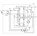
- Embodiment 1. 1 is a block diagram showing a configuration example of a rotating machine driving device 8 according to embodiment 1.
- the rotating machine driving device 8 is connected to an AC power source 1 and a load 4 including a motor 41.
- the rotating machine driving device 8 includes an AC/DC converter 2 and a DC/AC converter 3.
- the AC power source 1 is a single-phase AC power source that applies a power supply voltage to the AC/DC converter 2.
- the load 4 is a compressor or a fan
- the motor 41 is a compressor motor or a fan motor.
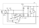
- the rectifier circuit 20 includes single-phase diode bridge cells 213a and 213b in which four diodes are bridge-connected, and a switching element 215 connected in parallel to both ends of the single-phase diode bridge cell 213b.
- the single-phase diode bridge cells 213a and 213b are connected in parallel to the AC power source 1.
- the rectifier circuit 20 as shown in FIG. 2 is called a "simple switching circuit.”
- the single-phase diode bridge cell 213b and the switching element 215 constitute a switching cell 225.
- the switching element 215 is disposed closer to the AC power source 1 than the capacitor 216.
- the switching element 215 performs a switching operation at least once per half cycle of the power source voltage. In this way, the rectifier circuit 20 has at least one switching element 215 and rectifies the power source voltage applied from the AC power source 1.
- the reactor 212 is disposed closer to the AC power source 1 than the capacitor 216.
- the rectifier circuit 20 receives the power supply voltage applied from the AC power source 1 via the reactor 212, and rectifies the received power supply voltage.
- the capacitor 216 is connected between the DC bus 9a and the DC bus 9b. The capacitor 216 smoothes the output voltage of the rectifier circuit 20.
- the control unit 6 receives the detection values of the voltage detection units 217a, 217b and the current detection unit 211. Based on each detection value, the control unit 6 generates a switching signal for controlling the on/off of the switching element 215.
- An example of the switching element 215 is an IGBT (Insulated Gate Bipolar Transistor) as shown in the figure, but is not limited to an IGBT. Any element capable of switching operation may be used as the switching element 215.
- Another example of the switching element 215 is a MOSFET (Metal-Oxide-Semiconductor Field-Effect Transistor).
- the AC-DC converter 2 shown in FIG. 2 is configured as a closed loop using the detection values of the voltage detectors 217a, 217b and the current detector 211, but may be configured as an open loop using target values, estimated values, etc. If the AC-DC converter 2 is configured as an open loop, it is also possible to control the switching element 215 without using the detection values of the voltage detectors 217a, 217b and the current detector 211.
- FIG. 3 is a diagram showing an example of the configuration of the AC-DC converter 2 according to embodiment 1 when viewed as a simplified PAM circuit.
- FIG. 3(a) shows a simplified PAM circuit
- FIG. 3(b) shows an equivalent circuit of the simplified PAM circuit shown in FIG. 3(a) when focusing on the DC component.
- the simplified PAM circuit is composed of two single-phase diode bridge cells 213a and 213b, which are two diode bridges, a switching element 215, which is a semiconductor switch, a reactor 212, and a capacitor 216.
- the simplified PAM circuit shown in FIG. 3(a) replaces the latter stage configuration, i.e., the capacitor 216, the DC-AC converter 3, and the load 4, with a voltage source 241.
- the equivalent circuit shown in FIG. 3(b) is a boost chopper consisting of a reactor 212, a switching element 215, and a diode 218, and the AC-DC converter 2 can design a current control system based on the control of the boost chopper.
- the voltage source 242 supplies the DC component of the power supply voltage from the AC power source 1.
- the reactor 212 is the plant, so a differential equation related to the reactor 212 may be derived.
- the inductance of the reactor 212 is L
- the power supply voltage from the AC power supply 1 is Vin
- the voltage applied to the single-phase diode bridge cell 213a is Vcnv
- the voltage applied to the reactor 212 is VL
- the voltage across the switching element 215 is VIGBT
- the output voltage is Vout
- the current flowing through the reactor 212 is iL
- the Laplace operator is s.
- the differential equation related to the reactor 212 is expressed by equation (1), and equation (1) is transformed into equation (2) by Laplace transformation.
- FIG. 4 is a diagram showing an example of a current control system of the boost chopper shown in FIG. 3(b).
- FIG. 4(a) is a current control plant obtained by Laplace transforming equation (2).
- FIG. 4(b) is a current control system in the case where a PI (Proportional Integral) controller is adopted as the current controller.
- K pACR is a proportional gain
- K iACR is an integral gain.
- the controller is not limited to PI control, and any controller such as proportional control, integral control, a sine wave tracking controller, or a two-degree-of-freedom controller may be used.
- the simple PAM circuit when the switching element 215 is off, the simple PAM circuit operates as a diode rectifier, and the current path of the simple PAM circuit is as shown in Fig. 6(a) or Fig. 6(c).
- the current path of the simple PAM circuit When the switching element 215 is on, the current path of the simple PAM circuit shorts the power supply as shown in Fig. 6(b) or Fig. 6(d), so that energy is stored in the reactor 212.
- the AC-DC converter 2 can boost the power supply voltage Vin by appropriately controlling the on/off of the switching element 215 and controlling the energy of the reactor 212.
- the voltage VL applied to the reactor 212 of the simplified PAM circuit can be expressed by equation (3) using the power supply voltage Vin of the AC power supply 1 and the converter voltage Vcnv . This relationship can also be confirmed from the operation waveforms in FIG.
- V L V in -V cnv (3)
- the first stage is a gate signal output from the control unit 6 to the switching element 215 so that the control unit 6 controls the on/off of the switching element 215,
- the second stage is a power supply voltage Vin of the AC power supply 1
- the third stage is a voltage VL applied to the reactor 212
- the fourth stage is a converter voltage Vcnv
- the fifth stage is a voltage VIGBT across the switching element 215
- the sixth stage is a power supply current of the AC power supply 1, which is a current iL flowing through the reactor 212.
- the converter voltage V cnv can be expressed by equation (4) using the sign function sign, the current i L flowing through the reactor 212, and the voltage V IGBT across the switching element 215.
- V cnv sign (i L ) ⁇ V IGBT (4)
- FIG. 8 is a diagram showing an example of a current controller provided in the control unit 6 of the AC-DC converter 2 according to the first embodiment.
- the power factor correction circuit it is necessary to control the current iL flowing through the reactor 212, which is the power supply current of the AC power supply 1, to be synchronized with the power supply voltage Vin of the AC power supply 1, so that the current command value is excited with a sine wave synchronized with the power supply voltage Vin of the AC power supply 1.
- the control unit 6 includes a current controller that controls the current of the AC power supply 1, which is a single-phase AC power supply, and changes the sign of a signal based on the output from the current controller according to the operating state of the AC-DC converter 2.
- the signal based on the output from the current controller is a duty, which is the voltage V IGBT across the switching element 215 input to the configuration of sign(iL) in FIG. 8.
- the control unit 6 changes the sign of the signal, i.e., the voltage V IGBT across the switching element 215, according to the polarity of the current i L flowing through the reactor 212 as the operating state of the AC-DC converter 2.
- the sign function sign changes depending on the polarity of the power supply voltage V in of the AC power supply 1.
- the converter voltage V cnv can be expressed by Equation (5) using the sign function sign, the power supply voltage V in of the AC power supply 1, and the voltage V IGBT across the switching element 215.
- Fig. 12 is a second diagram showing the relationship between the converter voltage Vcnv , which is the voltage applied to the single-phase diode bridge cell 213a in the simplified PAM circuit shown in Fig. 3(a), and the voltage VIGBT across the switching element 215.
- Fig. 12 is different from Fig. 7 in the part of the sign function sign in the equation expressing the converter voltage Vcnv .
- Embodiment 3 the control unit 6 of the AC-DC converter 2 changes the duty, i.e., the sign of the voltage V IGBT across the switching element 215 during current control, in accordance with the polarity of the current iL flowing through the reactor 212 as the operating state of the AC-DC converter 2.
- the control unit 6 of the AC-DC converter 2 changes the duty, i.e., the sign of the voltage V IGBT across the switching element 215 during current control, in accordance with the polarity of the power supply voltage V in of the AC power supply 1 as the operating state of the AC-DC converter 2.
- the control unit 6 changes the duty, i.e., the sign of the voltage V IGBT across the switching element 215, by using another parameter.
- V cnv sign (PLL) x V IGBT ...(6)
- the control unit 6 of the AC/DC converter 2 compensates the sign of the duty in accordance with the phase of the power supply voltage Vin of the AC power supply 1 estimated by the PLL, which is the AC power supply voltage phase estimation means, or the sine wave generated from the estimated phase, in order to realize current control in the simple PAM circuit.
- the control unit 6 changes the sign of the duty, i.e., the voltage V IGBT across the switching element 215, in accordance with the phase of the power supply voltage Vin of the AC power supply 1 estimated by the PLL, which is the AC power supply voltage phase estimation means, or the sine wave generated from the estimated phase.
- the AC/DC converter 2 realizes current control in the simple PAM circuit and enables quantitative control design.
- the AC/DC converter 2 can realize current control by the simple PAM circuit while being compliant with harmonic standards without relying on trial and error adjustment.
- the control unit 6 may change the duty, i.e., the sign of the voltage V IGBT across the switching element 215, in accordance with a phase after an operation to advance or delay the phase estimated by the PLL , which is the AC power supply voltage phase estimating means, or a sine wave generated from the phase after the operation.
- the control unit 6 can also change the sign of the voltage V IGBT across the switching element 215 by a combination of the polarity of the current i L flowing through the reactor 212 described in the first embodiment, the polarity of the power supply voltage V in of the AC power supply 1 described in the second embodiment, and the phase of the power supply voltage V in of the AC power supply 1 estimated by the PLL which is the AC power supply voltage phase estimation means described in the third embodiment, or a sine wave generated from the estimated phase.
- the control unit 6 may use all three combinations described in the first to third embodiments, or may use a combination of any two of the three combinations described in the first to third embodiments.
- FIG. 15 is a diagram showing an example of the configuration of an AC-DC converter 2 according to embodiment 4.
- the AC-DC converter 2 shown in FIG. 15 is obtained by deleting the single-phase diode bridge cell 213b from the AC-DC converter 2 shown in FIG. 2 and adding diodes 218a and 218b.
- the AC-DC converter 2 shown in FIG. 15 has a different method of connecting the switching element 215 from the AC-DC converter 2 shown in FIG. 2.
- the AC-DC converter 2 realizes current control in a simplified PAM circuit and enables quantitative control design by having the control unit 6 perform the control described in the first to third embodiments.
- the AC-DC converter 2 can achieve current control using a simplified PAM circuit while being compliant with harmonic standards without relying on trial-and-error adjustments.
- Embodiment 5 a different example of the AC-DC converter 2 including the control unit 6 described in the first to third embodiments will be described. Components having the same or equivalent functions as those of the AC-DC converter 2 described in the first to third embodiments will be denoted by the same reference numerals, and a description of the overlapping contents will be omitted.
- FIG. 16 is a diagram showing an example of the configuration of an AC-DC converter 2 according to embodiment 5.
- the AC-DC converter 2 shown in FIG. 16 is obtained by deleting the single-phase diode bridge cell 213b from the AC-DC converter 2 shown in FIG. 2 and adding a diode 218.
- the AC-DC converter 2 shown in FIG. 16 has a different connection method for the switching element 215 from the AC-DC converter 2 shown in FIG. 2.
- the AC-DC converter 2 realizes current control in a simplified PAM circuit and enables quantitative control design by having the control unit 6 perform the control described in the first to third embodiments.
- the AC-DC converter 2 can achieve current control using a simplified PAM circuit while being compliant with harmonic standards without relying on trial-and-error adjustments.
- the refrigeration cycle application device 900 includes a compressor 42 incorporating the motor 41 in the first embodiment, a four-way valve 902, an indoor heat exchanger 906, an expansion valve 908, and an outdoor heat exchanger 910 attached via refrigerant piping 912. Inside the compressor 42, there is provided a compression mechanism 904 that compresses the refrigerant, and a motor 41 that operates the compression mechanism 904.
- the refrigeration cycle application device 900 can perform heating or cooling operation by switching the four-way valve 902.
- the compression mechanism 904 is driven by a motor 41 that is variable speed controlled.
- the refrigerant is pressurized by the compression mechanism 904 and sent out, and returns to the compression mechanism 904 through the four-way valve 902, the indoor heat exchanger 906, the expansion valve 908, the outdoor heat exchanger 910, and the four-way valve 902.
- the refrigerant is pressurized by the compression mechanism 904 and sent out, and returns to the compression mechanism 904 through the four-way valve 902, the outdoor heat exchanger 910, the expansion valve 908, the indoor heat exchanger 906, and the four-way valve 902.
Landscapes
- Engineering & Computer Science (AREA)
- Power Engineering (AREA)
- Rectifiers (AREA)
Priority Applications (2)
| Application Number | Priority Date | Filing Date | Title |
|---|---|---|---|
| PCT/JP2023/047280 WO2025141869A1 (ja) | 2023-12-28 | 2023-12-28 | 交流直流変換装置、回転機駆動装置及び冷凍サイクル適用機器 |
| JP2025566165A JPWO2025141869A1 (https=) | 2023-12-28 | 2023-12-28 |
Applications Claiming Priority (1)
| Application Number | Priority Date | Filing Date | Title |
|---|---|---|---|
| PCT/JP2023/047280 WO2025141869A1 (ja) | 2023-12-28 | 2023-12-28 | 交流直流変換装置、回転機駆動装置及び冷凍サイクル適用機器 |
Publications (1)
| Publication Number | Publication Date |
|---|---|
| WO2025141869A1 true WO2025141869A1 (ja) | 2025-07-03 |
Family
ID=96217183
Family Applications (1)
| Application Number | Title | Priority Date | Filing Date |
|---|---|---|---|
| PCT/JP2023/047280 Pending WO2025141869A1 (ja) | 2023-12-28 | 2023-12-28 | 交流直流変換装置、回転機駆動装置及び冷凍サイクル適用機器 |
Country Status (2)
| Country | Link |
|---|---|
| JP (1) | JPWO2025141869A1 (https=) |
| WO (1) | WO2025141869A1 (https=) |
Citations (3)
| Publication number | Priority date | Publication date | Assignee | Title |
|---|---|---|---|---|
| JP2016144323A (ja) * | 2015-02-03 | 2016-08-08 | ジョンソンコントロールズ ヒタチ エア コンディショニング テクノロジー(ホンコン)リミテッド | 直流電源装置およびこれを用いた空気調和機 |
| WO2020070814A1 (ja) * | 2018-10-03 | 2020-04-09 | 三菱電機株式会社 | 電力変換器の制御装置及びフィードバック制御装置 |
| JP2022077586A (ja) * | 2020-11-12 | 2022-05-24 | 株式会社日本製鋼所 | 給電装置 |
-
2023
- 2023-12-28 WO PCT/JP2023/047280 patent/WO2025141869A1/ja active Pending
- 2023-12-28 JP JP2025566165A patent/JPWO2025141869A1/ja active Pending
Patent Citations (3)
| Publication number | Priority date | Publication date | Assignee | Title |
|---|---|---|---|---|
| JP2016144323A (ja) * | 2015-02-03 | 2016-08-08 | ジョンソンコントロールズ ヒタチ エア コンディショニング テクノロジー(ホンコン)リミテッド | 直流電源装置およびこれを用いた空気調和機 |
| WO2020070814A1 (ja) * | 2018-10-03 | 2020-04-09 | 三菱電機株式会社 | 電力変換器の制御装置及びフィードバック制御装置 |
| JP2022077586A (ja) * | 2020-11-12 | 2022-05-24 | 株式会社日本製鋼所 | 給電装置 |
Also Published As
| Publication number | Publication date |
|---|---|
| JPWO2025141869A1 (https=) | 2025-07-03 |
Similar Documents
| Publication | Publication Date | Title |
|---|---|---|
| CN103348578B (zh) | 逆流防止单元、电力变换装置以及制冷空气调节装置 | |
| EP2750279B1 (en) | Converter circuit and motor drive control apparatus, air-conditioner, refrigerator, and induction heating cooker provided with the circuit | |
| EP2624424B1 (en) | Power conversion device and refrigeration air-conditioning device | |
| US8164292B2 (en) | Motor controller of air conditioner | |
| US9998007B2 (en) | Boost converter with flying capacitor and refrigeration circuit | |
| EP3358732B1 (en) | Power conversion device and air-conditioning device using same | |
| WO2022091185A1 (ja) | 電力変換装置、モータ駆動装置および冷凍サイクル適用機器 | |
| JPWO2021038880A1 (ja) | 電力変換装置および空気調和機 | |
| KR20140096627A (ko) | 전력변환장치 및 이를 포함하는 공기조화기 | |
| WO2025141869A1 (ja) | 交流直流変換装置、回転機駆動装置及び冷凍サイクル適用機器 | |
| EP3826166B1 (en) | Power module and converter with asymmetrical semiconductor rating arrangement | |
| JPH0715966A (ja) | 電動機駆動装置 | |
| US20230246561A1 (en) | Power converter and heat pump system provided therewith | |
| JP7603906B1 (ja) | 交流直流変換装置、回転機駆動装置及び冷凍サイクル適用機器 | |
| JP6505264B2 (ja) | 電力変換装置およびこれを用いた空気調和装置 | |
| JP7603907B1 (ja) | 交流直流変換装置、回転機駆動装置及び冷凍サイクル適用機器 | |
| WO2025141871A1 (ja) | 交流直流変換装置、回転機駆動装置及び冷凍サイクル適用機器 | |
| WO2025141870A1 (ja) | 交流直流変換装置、回転機駆動装置及び冷凍サイクル適用機器 | |
| JP7774774B1 (ja) | 交流直流変換装置、回転機駆動装置、冷凍サイクル適用機器及び交流直流変換装置の制御方法 | |
| JP7625158B1 (ja) | 交流直流変換装置、回転機駆動装置及び冷凍サイクル適用機器 | |
| EP3121525B1 (en) | Power conversion apparatus and air conditioner including the same | |
| WO2025141868A1 (ja) | 交流直流変換装置、回転機駆動装置及び冷凍サイクル適用機器 | |
| WO2025141872A1 (ja) | 交流直流変換装置、回転機駆動装置及び冷凍サイクル適用機器 | |
| US20260063348A1 (en) | Method for controlling a compressor system, compressor for compressing a working medium, compressor system and refrigeration circuit system for carrying out a refrigeration cycle process | |
| Marimuthu et al. | Comparitive study of Single Phase Power Factor Correction based on Fixed and Variable PWM Techniques using Bridgeless Cuk Converter |
Legal Events
| Date | Code | Title | Description |
|---|---|---|---|
| 121 | Ep: the epo has been informed by wipo that ep was designated in this application |
Ref document number: 23963214 Country of ref document: EP Kind code of ref document: A1 |
|
| ENP | Entry into the national phase |
Ref document number: 2025566165 Country of ref document: JP Kind code of ref document: A |
|
| WWE | Wipo information: entry into national phase |
Ref document number: 2025566165 Country of ref document: JP |