WO2025134255A1 - 電磁波検出器及び電磁波検出器アレイ - Google Patents
電磁波検出器及び電磁波検出器アレイ Download PDFInfo
- Publication number
- WO2025134255A1 WO2025134255A1 PCT/JP2023/045632 JP2023045632W WO2025134255A1 WO 2025134255 A1 WO2025134255 A1 WO 2025134255A1 JP 2023045632 W JP2023045632 W JP 2023045632W WO 2025134255 A1 WO2025134255 A1 WO 2025134255A1
- Authority
- WO
- WIPO (PCT)
- Prior art keywords
- semiconductor layer
- electromagnetic wave
- dimensional material
- layer
- material layer
- Prior art date
- Legal status (The legal status is an assumption and is not a legal conclusion. Google has not performed a legal analysis and makes no representation as to the accuracy of the status listed.)
- Pending
Links
Images


Definitions
- This disclosure relates to electromagnetic wave detectors and electromagnetic wave detector arrays.
- Patent Document 1 proposes a detector with the following structure. That is, in the detector of Patent Document 1, two or more dielectric layers are provided on an n-type semiconductor layer. A graphene layer is formed on the two dielectric layers and on the surface portion of the n-type semiconductor layer located between the two dielectric layers.
- the graphene layer and the n-type semiconductor layer are connected to a Schottky junction.
- Source and drain electrodes connected to both ends of the graphene layer are arranged on the dielectric layer.
- the gate electrode is connected to the n-type semiconductor layer.
- the sensitivity of the detector depends on the quantum efficiency of the semiconductor layer. As a result, photocarriers cannot be sufficiently amplified, making it difficult to increase the sensitivity of the detector.
- This disclosure proposes technology that improves detection sensitivity compared to the above detectors.
- the electromagnetic wave detector includes a first semiconductor layer having a first surface and a second surface located opposite the first surface, a first insulating layer disposed on the first surface and having a first opening formed therein, a first two-dimensional material layer electrically connected to the first semiconductor layer at the first opening and extending from above the first opening to above the first insulating layer, a first electrode electrically connected to the first two-dimensional material layer without the first semiconductor layer, a second semiconductor layer having a third surface and a fourth surface located opposite the third surface, a second insulating layer disposed on the third surface and having a second opening formed therein, a second two-dimensional material layer electrically connected to the second semiconductor layer at the second opening and extending from above the second opening to above the second insulating layer, and a second electrode electrically connected to the second two-dimensional material layer without the second semiconductor layer.
- the first semiconductor layer and the second semiconductor layer are stacked such that the second surface and the fourth surface overlap each other.
- detection sensitivity can be improved compared to the above detector.
- FIG. 1 is a schematic cross-sectional view of an electromagnetic wave detector 100 according to a first embodiment.
- 1 is a schematic plan view of an electromagnetic wave detector 100 according to a first embodiment.
- 2 is a schematic bottom view of the electromagnetic wave detector 100 according to the first embodiment.
- FIG. 4 is a flowchart for explaining a method for manufacturing the electromagnetic wave detector according to the first embodiment.
- FIG. 11 is a schematic cross-sectional view of an electromagnetic wave detector 101 according to a second embodiment.
- FIG. 11 is a schematic cross-sectional view of an electromagnetic wave detector 102 according to a third embodiment.
- FIG. 11 is a schematic cross-sectional view of an electromagnetic wave detector 103 according to a fourth embodiment.
- FIG. 13 is a schematic plan view of an electromagnetic wave detector 104 according to a fifth embodiment.
- FIG. 13 is a schematic cross-sectional view of an electromagnetic wave detector 104 according to a fifth embodiment.
- FIG. 13 is a schematic plan view of a modified example of the electromagnetic wave detector 104 according to the fifth embodiment.
- FIG. 13 is a schematic cross-sectional view of a modified example of the electromagnetic wave detector 104 according to the fifth embodiment.
- FIG. 13 is a schematic plan view of an electromagnetic wave detector 105 according to a sixth embodiment.
- FIG. 13 is a schematic cross-sectional view of an electromagnetic wave detector 105 according to a sixth embodiment.
- FIG. 13 is a schematic plan view of an electromagnetic wave detector 106 according to a seventh embodiment.
- FIG. 13 is a schematic bottom view of an electromagnetic wave detector 106 according to a seventh embodiment.
- FIG. 13 is a schematic cross-sectional view of an electromagnetic wave detector 106 according to a seventh embodiment.
- FIG. 13 is a schematic cross-sectional view of an electromagnetic wave detector 107 according to an eighth embodiment.
- 13 is a plan view illustrating an electromagnetic wave detector array according to a ninth embodiment.
- FIG. 13 is a schematic plan view showing a modified example of an electromagnetic wave detector array according to embodiment 9.
- an electromagnetic wave detector that detects visible light or infrared light as electromagnetic waves is described, but the electromagnetic waves detected by the electromagnetic wave detector of the present disclosure are not limited to visible light and infrared light.
- the embodiments described below are also effective as a detector that detects radio waves such as X-rays, ultraviolet light, near-infrared light, terahertz (THz) waves, and microwaves, in addition to visible light and infrared light. Note that in the embodiments described below, these lights and radio waves are collectively referred to as electromagnetic waves.
- the material of the two-dimensional material layer is described as graphene, but the material constituting the two-dimensional material layer is not limited to graphene.
- the material of the two-dimensional material layer can be a transition metal dichalcogenide (TMD), black phosphorus, silicene (two-dimensional honeycomb structure of silicon atoms), germanene (two-dimensional honeycomb structure of germanium atoms), etc.
- TMD transition metal dichalcogenide
- Examples of the transition metal dichalcogenide include MoS 2 , WS 2 , and WSe 2 .
- These materials have a structure similar to that of graphene, and are capable of arranging atoms in a single layer on a two-dimensional surface. Therefore, even when these materials are applied to a two-dimensional material layer, it is possible to obtain the same effects as when graphene is applied to a two-dimensional material layer.
- the two-dimensional material layer may be composed of two-dimensional materials arranged in a single layer (e.g., single-layer graphene).
- the two-dimensional material layer may be composed of two-dimensional materials arranged in multiple layers (e.g., multi-layer graphene).
- the photoelectric conversion efficiency increases, and the sensitivity of the electromagnetic wave detector increases.
- a band gap is formed in the latter two-dimensional material layer.
- the latter two-dimensional material layer can be provided so that photoelectric conversion occurs in the two-dimensional material layer only when electromagnetic waves in a predetermined wavelength range are incident on the two-dimensional material layer.
- the detection sensitivity of electromagnetic waves can be increased.
- the orientation of the hexagonal lattice vector between any two graphene layers may or may not match each other.
- the stacking orientation angle may be not only AB stacking seen in graphite in its natural state, but also turbostratic stacking. Turbostratic stacking is also called random stacking or turbostratic graphene.
- the method for producing the turbostratic structure portion may be determined appropriately. For example, a single layer of graphene produced by the CVD method may be transferred multiple times, and multilayer graphene may be stacked to form the turbostratic structure portion. Also, ethanol or methane may be placed on the graphene as a carbon source, and the graphene may be grown by the CVD method to form the turbostratic structure portion.
- the stacking orientation angle may also be an angle that generates moire.
- a flat band is formed, and the incident light can be coupled in a wide range of wavelengths, improving the efficiency of the photodetector. Furthermore, a specific wavelength range can be selectively detected by forming a moire potential depending on the stacking orientation angle.
- p-type and n-type may be used for the two-dimensional material layer.
- a two-dimensional material layer having more holes than a two-dimensional material layer in an intrinsic state is called p-type
- n-type a two-dimensional material layer having more electrons than a two-dimensional material layer in an intrinsic state
- the two-dimensional material layer may be intrinsic, i.e., not doped with impurities, and may have a conductivity type of p-type or n-type.
- n-type and p-type may be used to describe the materials of components in contact with the two-dimensional material layer.
- n-type materials refer to materials that have electron-donating properties
- p-type materials refer to materials that have electron-attracting properties.
- n-type there are cases where there is a bias in the charge throughout the molecule, and those in which electrons are predominant are called n-type, and those in which holes are predominant are called p-type.
- These materials can be either organic or inorganic, or a mixture of both.
- the two-dimensional material layer when the two-dimensional material layer is in contact with an electrode, carriers are doped from the electrode into the two-dimensional material layer.
- carriers are doped from the electrode into the two-dimensional material layer.
- Au gold
- holes are doped into the two-dimensional material layer near the electrode due to the difference in work function between the two-dimensional material layer and Au.
- the electromagnetic wave detector is driven in an electronic conduction state in this state, the influence of the holes doped from the electrode into the two-dimensional material layer reduces the mobility of electrons flowing into the channel region of the two-dimensional material layer, and the contact resistance between the two-dimensional material layer and the electrode increases.
- This increase in contact resistance reduces the mobility of electrons (carriers) due to the field effect in the electromagnetic wave detector, which may cause a decrease in performance of the electromagnetic wave detector.
- the doping amount of carriers injected from the electrode is larger than when the two-dimensional material layer is made of multi-layer graphene. Therefore, the decrease in the mobility of the electrons in the electromagnetic wave detector is particularly noticeable when single-layer graphene is used as the two-dimensional material layer. Therefore, if the entire two-dimensional material layer is made of single-layer graphene, the performance of the electromagnetic wave detector may be degraded. Therefore, at least the contact area with the electrode of the secondary raw material layer may be made of multi-layer graphene.
- carrier doping from the electrode is smaller than in single-layer graphene. Therefore, an increase in the contact resistance between the two-dimensional material layer and the electrode can be suppressed. As a result, the above-mentioned decrease in the mobility of electrons in the electromagnetic wave detector can be suppressed, and the performance of the electromagnetic wave detector can be improved.
- the two-dimensional material layer may also include nanoribbon-shaped graphene (hereinafter also referred to as graphene nanoribbons).
- the two-dimensional material layer may be, for example, a single graphene nanoribbon, a composite in which multiple graphene nanoribbons are stacked, or a structure in which graphene nanoribbons are periodically arranged on a plane (for example, a graphene metamaterial).
- a two-dimensional material layer configured as a structure in which graphene nanoribbons are periodically arranged on a plane plasmon resonance may occur. As a result, the sensitivity of the electromagnetic wave detector can be improved.
- plasmon resonance phenomena such as surface plasmon resonance, which is an interaction between a metal surface and light, a phenomenon called pseudo-surface plasmon resonance, which means resonance on a metal surface outside the visible light and near-infrared light ranges, and a phenomenon called metamaterials or plasmonic metamaterials, which means the manipulation of specific wavelengths using a structure with dimensions smaller than the wavelength, are not differentiated by name, but are treated as equivalent in terms of the effects of the phenomenon.
- these resonances are called surface plasmon resonance, plasmon resonance, or simply resonance.
- an insulating layer is a layer of insulating film that has a thickness that does not generate tunneling current.
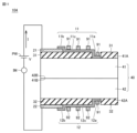
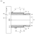
- Fig. 1 is a schematic cross-sectional view of an electromagnetic wave detector 100 according to embodiment 1.
- Fig. 1 also shows typical electrical connections of the electromagnetic wave detector 100.
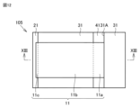
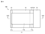
- Fig. 2 is a schematic plan view of the electromagnetic wave detector 100 shown in Fig. 1.
- Fig. 3 is a schematic bottom view of the electromagnetic wave detector 100 shown in Fig. 1.
- the electromagnetic wave detector 100 mainly comprises a first two-dimensional material layer 11, a first electrode 21, a second electrode 22, a first insulating layer 31, a second insulating layer 32, and a light receiving element 40.
- the light receiving element 40 has a first surface 41A and a second surface 42A located on the opposite side to the first surface 41A.
- the light receiving element 40 includes a first semiconductor layer 41 having the first surface 41A and a second semiconductor layer 42 having the second surface 42A.
- the first semiconductor layer 41 further has a third surface 41B located on the opposite side to the first surface 41A.
- the first two-dimensional material layer 11, the first electrode 21, and the first insulating layer 31 are disposed on the first surface 41A.
- the portions located on the opposite side to the first semiconductor layer 41 are described as the upper portions, and the portions located on the first semiconductor layer 41 side are described as the lower portions.
- the viewpoint of viewing the first surface 41A from a direction perpendicular to the first surface 41A, or the viewpoint of viewing the second surface 42A from a direction perpendicular to the second surface 42A is described as a planar view.
- the second semiconductor layer 42 further has a fourth surface 42B located on the opposite side to the second surface 42A.
- the second two-dimensional material layer 12, the second electrode 22, and the second insulating layer 32 are disposed on the second surface 42A.
- the portions located on the opposite side to the second semiconductor layer 42 are referred to as the upper portions, and the portions located on the second semiconductor layer 42 side are referred to as the lower portions.
- the first semiconductor layer 41 and the second semiconductor layer 42 are stacked such that the third surface 41B and the fourth surface 42B overlap each other.
- the third surface 41B faces the fourth surface 42B.
- the entire surface of the third surface 41B overlaps the entire surface of the fourth surface 42B. It is sufficient that the third surface 41B overlaps at least a portion of the fourth surface 42B.
- the light receiving element 40 is an element that is sensitive to electromagnetic waves of the detection wavelength of the electromagnetic wave detector 100 and performs photoelectric conversion when irradiated with electromagnetic waves of the detection wavelength.
- the light receiving element 40 of the electromagnetic wave detector 100 includes a pn junction photodiode.
- the fourth surface 42B of the second semiconductor layer 42 is in contact with the third surface 41B of the first semiconductor layer 41.
- the first semiconductor layer 41 has a first conductivity type.
- the second semiconductor layer 42 has a second conductivity type different from the first conductivity type.
- the first conductivity type of the first semiconductor layer 41 may be p type, and the second conductivity type of the second semiconductor layer 42 may be n type.
- the first conductivity type of the first semiconductor layer 41 may be n type, and the second conductivity type of the second semiconductor layer 42 may be p type.
- a pn junction is formed at the interface between the third surface 41B of the first semiconductor layer 41 and the fourth surface 42B of the second semiconductor layer 42.
- the light receiving element 40 may include a pin photodiode, a Schottky photodiode, an avalanche photodiode, or a phototransistor.
- the materials constituting the first semiconductor layer 41 and the second semiconductor layer 42 can be selected arbitrarily depending on the detection wavelength of the electromagnetic wave detector 100.
- the material constituting the first semiconductor layer 41 may be the same as the material constituting the second semiconductor layer 42.
- the material constituting the first semiconductor layer 41 may be different from the material constituting the second semiconductor layer 42. In the latter case, the electromagnetic wave detector 100 becomes capable of detecting multiple wavelengths.
- the materials constituting the first semiconductor layer 41 and the second semiconductor layer 42 are, for example, Si, germanium (Ge), compound semiconductors such as III-V or II-V group semiconductors, mercury cadmium telluride (HgCdTe), indium antimony (InSb), lead selenium (PbSe), lead sulfur (PbS), cadmium sulfur (CdS), gallium nitride (GaN), silicon carbide (SiC), gallium phosphide (GaP), indium gallium arsenide (InGaAs), indium arsenide (InAs), or a substrate containing quantum wells or quantum dots, a Type II superlattice, or a combination of these materials.
- the material constituting at least one of the first semiconductor layer 41 and the second semiconductor layer 42 may contain InGaAs.
- the material constituting at least one of the first semiconductor layer 41 and the second semiconductor layer 42 may contain InAs.
- the material constituting at least one of the first semiconductor layer 41 and the second semiconductor layer 42 may contain InSb.
- the material constituting at least one of the first semiconductor layer 41 and the second semiconductor layer 42 may contain HgCdTe.
- each of the first semiconductor layer 41 and the second semiconductor layer 42 is preferably 10 ⁇ m or less.
- the first insulating layer 31 is disposed on the first surface 41A of the first semiconductor layer 41.
- the lower surface of the first insulating layer 31 is in contact with the first surface 41A of the first semiconductor layer 41.
- the upper surface of the first insulating layer 31 is in contact with, for example, the third portion 11c of the first two-dimensional material layer 11 described below and the lower surface of each of the first electrodes 21.
- a first opening 31A is formed in the first insulating layer 31.
- the first opening 31A exposes a portion of the first surface 41A.
- the second insulating layer 32 is disposed on the second surface 42A of the second semiconductor layer 42.
- the lower surface of the second insulating layer 32 is in contact with the second surface 42A of the second semiconductor layer 42.
- the upper surface of the second insulating layer 32 is in contact with, for example, a sixth portion 12c of the second two-dimensional material layer 12 described below and the lower surface of each of the second electrodes 22.
- a second opening 32A is formed in the second insulating layer 32.
- the second opening 32A exposes a portion of the second surface 42A.
- the material constituting the first insulating layer 31 and the second insulating layer 32 may be any material having electrical insulation properties, and may include, for example, silicon oxide (SiO 2 ).
- the material constituting the first insulating layer 31 may include, for example, at least one selected from the group consisting of SiO 2 , tetraethyl orthosilicate (Si(OC 2 H 5 ) 4 ), silicon nitride (Si 3 N 4 ), hafnium oxide (HfO 2 ), aluminum oxide (Al 2 O 3 ), nickel oxide (NiO), boron nitride (BN) (boron nitride), and siloxane-based polymer materials.
- the atomic arrangement of boron nitride is similar to that of graphene, so that even if boron nitride comes into contact with a two-dimensional material layer made of graphene, it does not adversely affect the mobility of charges. Therefore, from the viewpoint of preventing the first insulating layer 31 and the second insulating layer 32 from impairing the performance of the first two-dimensional material layer 11 and the second two-dimensional material layer 12, such as electron mobility, boron nitride is suitable as a material for constituting the first insulating layer 31 and the second insulating layer 32.
- the thickness of the first insulating layer 31 is not particularly limited as long as no tunnel current occurs in the region of the first two-dimensional material layer 11 located on the first insulating layer 31 (second portion 11b and third portion 11c described below) and between the first electrode 21 and the first semiconductor layer 41. From the viewpoint of enhancing the optical gate effect described below and increasing the degree of electric field change occurring in the first two-dimensional material layer 11, it is preferable that the thickness of the first insulating layer 31 is as thin as possible.
- the thickness of the second insulating layer 32 is not particularly limited as long as no tunnel current occurs in the region of the second two-dimensional material layer 12 located on the second insulating layer 32 (the fifth portion 12b and the sixth portion 12c described below) and between the second electrode 22 and the second semiconductor layer 42. From the viewpoint of enhancing the optical gate effect described below and increasing the degree of the electric field change occurring in the second two-dimensional material layer 12, it is preferable that the thickness of the second insulating layer 32 is as thin as possible.
- the first electrode 21 is disposed on the upper surface of the first insulating layer 31.
- the first electrode 21 is formed, for example, in the lower part of the first two-dimensional material layer 11.
- the second electrode 22 is disposed on the upper surface of the second insulating layer 32.
- the second electrode 22 is formed, for example, in the lower part of the second two-dimensional material layer 12.
- the first electrode 21 may be formed in the upper part of the first two-dimensional material layer 11.
- the second electrode 22 may be formed in the upper part of the second two-dimensional material layer 12.
- the first electrode 21 is disposed so as to overlap the second electrode 22, for example, in a direction perpendicular to the first surface 41A.
- the first electrode 21 may be disposed so as not to overlap the second electrode 22 in a direction perpendicular to the first surface 41A.
- the material constituting the first electrode 21 and the second electrode 22 may be any material having electrical conductivity, and may include, for example, at least one selected from the group consisting of gold (Au), silver (Ag), copper (Cu), aluminum (Al), nickel (Ni), chromium (Cr), and palladium (Pd).
- an adhesion layer (not shown) may be formed between the first electrode 21 and the first insulating layer 31, and between the second electrode 22 and the second insulating layer 32, in order to improve adhesion therebetween.
- the material constituting the adhesion layer is not particularly limited, and may include, for example, at least one of chromium (Cr) and titanium (Ti).
- the area of the first electrode 21 is, for example, equal to or larger than the area of the first opening 31A.
- the area of the second electrode 22 is, for example, equal to or larger than the area of the second opening 32A.
- a power supply circuit for applying a bias voltage V to the first two-dimensional material layer 11 and the second two-dimensional material layer 12 is electrically connected between the first electrode 21 and the second electrode 22 of the first set.
- the power supply circuit includes a voltage source PW and an ammeter IM.
- the voltage source PW applies the bias voltage V between the first electrode 21 and the second electrode 22.
- the ammeter IM detects the current I that flows when the bias voltage V is applied between the first electrode 21 and the second electrode 22.
- the first two-dimensional material layer 11 is electrically connected to the first semiconductor layer 41 at the first opening 31A.
- the first two-dimensional material layer 11 extends from above the first opening 31A onto the first insulating layer 31.
- the second two-dimensional material layer 12 is electrically connected to the second semiconductor layer 42 at the second opening 32A.
- the second two-dimensional material layer 12 extends from above the second opening 32A onto the second insulating layer 32.
- the first two-dimensional material layer 11 has a first portion 11a electrically connected to the first semiconductor layer 41, a second portion 11b electrically connected to the first electrode 21, and a third portion 11c electrically connecting the first portion 11a and the second portion 11b.
- the second portion 11b and the third portion 11c are disposed on the first insulating layer 31.
- the third portion 11c is in contact with, for example, the upper surface of the first insulating layer 31.
- the third portion 11c acts as a channel of the field effect transistor.
- the first portion 11a and the second portion 11b act as a source and a drain of the field effect transistor.
- the upper surface of the first two-dimensional material layer 11 has irregularities due to, for example, the first electrode 21 and the first insulating layer 31.
- the first portion 11a includes, for example, one end of the first two-dimensional material layer 11.
- the second portion 11b includes, for example, the other end of the first two-dimensional material layer 11.
- the one end of the first two-dimensional material layer 11 is in contact with, for example, the inner circumferential surface of the first opening 31A of the first insulating layer 31.
- the first two-dimensional material layer 11 is located on the opposite side of the first portion 11a to the third portion 11c, is disposed on the first insulating layer 31, and may further have a portion including the one end of the first two-dimensional material layer 11.
- the second two-dimensional material layer 12 has a fourth portion 12a electrically connected to the second semiconductor layer 42, a fifth portion 12b electrically connected to the second electrode 22, and a sixth portion 12c electrically connecting the fourth portion 12a and the fifth portion 12b.
- the second portion 11b and the third portion 11c of the first two-dimensional material layer 11 are disposed on the first insulating layer 31.
- the third portion 11c is in contact with, for example, the upper surface of the first insulating layer 31.
- the sixth portion 12c acts as a channel of the field effect transistor.
- the fourth portion 12a and the fifth portion 12b act as a source and a drain of the field effect transistor.
- the upper surface of the second two-dimensional material layer 12 has irregularities due to, for example, the second electrode 22 and the second insulating layer 32.
- the fourth portion 12a includes, for example, one end of the second two-dimensional material layer 12.
- the fifth portion 12b includes, for example, the other end of the second two-dimensional material layer 12.
- the one end of the second two-dimensional material layer 12 is in contact with, for example, the inner circumferential surface of the second opening 32A of the second insulating layer 32.
- the second two-dimensional material layer 12 is located on the opposite side of the sixth portion 12c with respect to the fourth portion 12a, is disposed on the second insulating layer 32, and may further have a portion including the one end of the second two-dimensional material layer 12.
- Each of the first two-dimensional material layer 11 and the second two-dimensional material layer 12 has sensitivity to electromagnetic waves of the detection wavelength, and is configured to perform photoelectric conversion when electromagnetic waves of the detection wavelength are incident. At least one of the first two-dimensional material layer 11 and the second two-dimensional material layer 12 may be configured to perform photoelectric conversion only when electromagnetic waves of the detection wavelength are incident.
- the thicknesses of the first portion 11a, the second portion 11b, and the third portion 11c of the first two-dimensional material layer 11 are, for example, equal to each other.
- the thicknesses of the fourth portion 12a, the fifth portion 12b, and the sixth portion 12c of the second two-dimensional material layer 12 are, for example, equal to each other.
- the thicknesses of the first portion 11a, the second portion 11b, and the third portion 11c of the first two-dimensional material layer 11 are, for example, equal to the thicknesses of the fourth portion 12a, the fifth portion 12b, and the sixth portion 12c of the second two-dimensional material layer 12.
- the thicknesses of the first portion 11a, the second portion 11b, and the third portion 11c of the first two-dimensional material layer 11 may be different from each other.
- the thicknesses of the fourth portion 12a, the fifth portion 12b, and the sixth portion 12c of the second two-dimensional material layer 12 may be different from each other.
- the thickness of each of the first portion 11a, the second portion 11b, and the third portion 11c of the first two-dimensional material layer 11 may be different from the thickness of each of the fourth portion 12a, the fifth portion 12b, and the sixth portion 12c of the second two-dimensional material layer 12.
- the electromagnetic wave detector 100 has symmetry with the interface between the third surface 41B and the fourth surface 42B as the mirror plane, for example.
- the portion located on the first semiconductor layer 41 side of the interface has a mirror image symmetric relationship with the portion located on the second semiconductor layer 42 side of the interface.
- the first portion 11a, the second portion 11b, and the third portion 11c of the first two-dimensional material layer 11 are arranged to overlap, for example, the fourth portion 12a, the fifth portion 12b, and the sixth portion 12c of the second two-dimensional material layer 12, respectively.
- the first opening 31A is arranged to overlap, for example, the second opening 32A.
- the first electrode 21 is arranged to overlap, for example, the second electrode 22.
- Each of the first two-dimensional material layer 11 and the second two-dimensional material layer 12 has a conductivity type of, for example, p-type or n-type.
- the conductivity type of the first two-dimensional material layer 11 is different from the conductivity type of the first semiconductor layer 41, for example.
- the conductivity type of the first semiconductor layer 41 is n-type
- the conductivity type of the first two-dimensional material layer 11 is, for example, p-type.
- the conductivity type of the first semiconductor layer 41 is p-type
- the conductivity type of the first two-dimensional material layer 11 is, for example, n-type.
- the conductivity type of the first two-dimensional material layer 11 may be the same as the conductivity type of the first semiconductor layer 41, for example.
- the conductivity type of the first semiconductor layer 41 When the conductivity type of the first semiconductor layer 41 is n-type, the conductivity type of the first two-dimensional material layer 11 may be n-type. When the conductivity type of the first semiconductor layer 41 is p-type, the conductivity type of the first two-dimensional material layer 11 may be p-type.
- the conductivity type of the second two-dimensional material layer 12 may also be different from or the same as the conductivity type of the second semiconductor layer 42.
- the conductivity type of the first two-dimensional material layer 11 is, for example, the same as the conductivity type of the second two-dimensional material layer 12. Note that the conductivity type of the first two-dimensional material layer 11 may be different from the conductivity type of the second two-dimensional material layer 12.
- the two-dimensional surface of the first two-dimensional material layer 11 is aligned with the top surface of the first two-dimensional material layer 11.
- the absolute value of the angle that the two-dimensional surface of the first two-dimensional material layer 11 forms with respect to the top surface of the first two-dimensional material layer 11 is greater than or equal to 0° and less than or equal to 10°.
- the two-dimensional surface of the first two-dimensional material layer 11 is, for example, parallel to the top surface of the first two-dimensional material layer 11.
- the two-dimensional surface of the second two-dimensional material layer 12 is aligned with the top surface of the second two-dimensional material layer 12.
- the absolute value of the angle that the two-dimensional surface of the second two-dimensional material layer 12 forms with respect to the top surface of the second two-dimensional material layer 12 is greater than or equal to 0° and less than or equal to 10°.
- the two-dimensional surface of the second two-dimensional material layer 12 is, for example, parallel to the top surface of the second two-dimensional material layer 12.
- a step (S1) of preparing the second semiconductor layer 42 is carried out.
- the second semiconductor layer 42 is prepared as a flat substrate made of, for example, Si.
- a protective film may be formed on the surface of the second semiconductor layer 42.
- a step (S4) of forming the first electrode 21 is carried out.
- the first electrode 21 is formed on the first insulating layer 31.
- the material constituting the first electrode 21 is, for example, a metal such as gold (Au), silver (Ag), copper (Cu), aluminum (Al), nickel (Ni), or chromium (Cr).
- an adhesion layer may be formed between the first insulating layer 31 and the first electrode 21.
- the material constituting the adhesion layer may be, for example, chromium (Cr) or titanium (Ti).
- a step (S5) of forming the first opening 31A is performed.
- the first opening 31A is formed in the first insulating layer 31.
- a resist mask is formed on the first insulating layer 31 using photolithography or EB drawing.
- An opening is formed in the resist mask in the area where the first opening 31A of the first insulating layer 31 is to be formed.
- the first insulating layer 31 is partially removed by wet etching or dry etching using the resist mask as a mask to form the first opening 31A.
- the resist mask is removed. Note that the above step (S5) may be performed prior to step (S4).
- a step (S6) of forming a first two-dimensional material layer 11 is performed.
- the first two-dimensional material layer 11 is formed so as to cover the entire portion of the first electrode 21, the first insulating layer 31, and the first semiconductor layer 41 exposed in the first opening 31A.
- the first two-dimensional material layer 11 may be formed by any method.
- the first two-dimensional material layer 11 may be formed by epitaxial growth, or the first two-dimensional material layer 11 formed in advance using a CVD method may be transferred and attached onto a portion of the first electrode 21, the first insulating layer 31, and the first semiconductor layer 41.
- the first two-dimensional material layer 11 may be formed using screen printing or the like.
- the first two-dimensional material layer 11 peeled off by mechanical peeling or the like may be transferred onto the above-mentioned first electrode 21, etc.
- a resist mask is formed on the first two-dimensional material layer 11 using photolithography or the like.
- the resist mask is formed so as to cover the areas where the first two-dimensional material layer 11 is to remain, but is not formed in the areas where the first two-dimensional material layer 11 is not to remain.
- the first two-dimensional material layer 11 is partially removed by etching with oxygen plasma. This removes unnecessary parts of the two-dimensional material layer, and forms the first two-dimensional material layer 11 as shown in Figures 1 to 3. Then, the resist mask is removed.
- a step (S7) of forming the second insulating layer 32 is performed.
- the second insulating layer 32 is formed on the second semiconductor layer 42.
- the second insulating layer 32 may be formed by at least one of a CVD method and a sputtering method, for example.
- the second insulating layer 32 may be, for example, SiO 2 formed by partially thermally oxidizing the second surface 42A of the second semiconductor layer 42.
- a step (S8) of forming the second electrode 22 is performed.
- the second electrode 22 is formed on the second insulating layer 32.
- the material constituting the first electrode 21 is, for example, a metal such as gold (Au), silver (Ag), copper (Cu), aluminum (Al), nickel (Ni), or chromium (Cr).
- an adhesion layer may be formed between the first insulating layer 31 and the first electrode 21.
- the material constituting the adhesion layer may be, for example, chromium (Cr) or titanium (Ti).
- the method of forming the second electrode 22 may be selected in the same manner as the method of forming the first electrode 21 described above.
- a step (S9) of forming the second opening 32A is performed.
- the second opening 32A is formed in the second insulating layer 32.
- a resist mask is formed on the second insulating layer 32 using photolithography or EB drawing.
- An opening is formed in the resist mask in the area where the second opening 32A of the second insulating layer 32 is to be formed.
- the second insulating layer 32 is partially removed by wet etching or dry etching using the resist mask as a mask to form the second opening 32A.
- the resist mask is removed. Note that the above step (S9) may be performed prior to step (S8).
- the second two-dimensional material layer 12 peeled off by mechanical peeling or the like may be transferred onto the above-mentioned second electrode 22, etc.
- a resist mask is formed on the second two-dimensional material layer 12 by photolithography or the like.
- the resist mask is formed to cover the areas where the second two-dimensional material layer 12 is to remain, but is not formed in the areas where the second two-dimensional material layer 12 is not to remain.
- the second two-dimensional material layer 12 is partially removed by etching with oxygen plasma. This removes unnecessary parts of the two-dimensional material layer, forming the second two-dimensional material layer 12 as shown in Figures 1 and 2. Then, the resist mask is removed.
- the first two-dimensional material layer 11 is formed on the first electrode 21, but the first two-dimensional material layer 11 may be formed in advance on the first insulating layer 31, and the first electrode 21 may be formed so as to overlap a portion of the first two-dimensional material layer 11.
- care must be taken not to cause process damage to the first two-dimensional material layer 11 when forming the first electrode 21.
- a power supply circuit that applies a bias voltage V is electrically connected between the first electrode 21 and the second electrode 22.
- a current I flows through the first two-dimensional material layer 11 and the second two-dimensional material layer 12.
- An ammeter IM included in the power supply circuit monitors the current I flowing through the first two-dimensional material layer 11 and the second two-dimensional material layer 12.
- the light receiving element 40 also applies an electric field change to the first two-dimensional material layer 11 through the first insulating layer 31, and further applies an electric field change to the second two-dimensional material layer 12 through the second insulating layer 32.
- a state in which a pseudo gate voltage is applied to each of the first two-dimensional material layer 11 and the second two-dimensional material layer 12 is created, and the resistance values of each of the first two-dimensional material layer 11 and the second two-dimensional material layer 12 change. This is called the optical gate effect.
- the change in the resistance value of each of the first two-dimensional material layer 11 and the second two-dimensional material layer 12 changes the current I flowing through the first two-dimensional material layer 11 and the second two-dimensional material layer 12. By detecting this change in current I, the electromagnetic wave irradiated to the electromagnetic wave detector 100 can be detected.
- the current I can be made zero by adjusting the voltage V and operating the light receiving element 40 in reverse bias. In other words, the electromagnetic wave detector 100 can be turned off. At this time, a current flows through the light receiving element 40 only when light is irradiated, so the current I can be detected only when light is irradiated.
- the range of detection wavelengths of the electromagnetic wave detector is determined according to the constituent material of the light receiving element 40.
- the detection wavelength of an electromagnetic wave detector having a light receiving element 40 with the above-described configuration is 0.2 ⁇ m or more and 1.1 ⁇ m or less.
- the photocarriers generated in the region directly below the first insulating layer 31 cause an electric field change in the first two-dimensional material layer 11 through the first insulating layer 31. Furthermore, the photocarriers generated in the region directly below the second insulating layer 32 cause an electric field change in the second two-dimensional material layer 12 through the second insulating layer 32.
- the two-dimensional material e.g., graphene
- the two-dimensional material constituting the first two-dimensional material layer 11 and the second two-dimensional material layer 12 has high mobility, and a large displacement current can be obtained for a slight electric field change.
- the photocurrent extracted from the first electrode 21 through the first two-dimensional material layer 11 and the second two-dimensional material layer 12 by photoelectric conversion in the light receiving element 40 is greatly amplified by the optical gate effect. Therefore, in the electromagnetic wave detector 100, it is possible to achieve high sensitivity that exceeds the quantum efficiency of silicon.
- the light receiving element 40 it is preferable to design the light receiving element 40 so that the carrier diffusion length is short.
- the carrier diffusion length By shortening the carrier diffusion length, the carrier lifetime of the photocarriers in the light receiving element 40 is shortened.
- the delay in amplification due to the optical gate effect is eliminated, and the optical carriers generated by the photoelectric conversion of the light receiving element 40 and the amplification due to the optical gate effect can be separated, enabling the electromagnetic wave detector 100 to have a high-speed response.
- the electromagnetic wave detector 100 when an electromagnetic wave of a detection wavelength is incident on the light receiving element 40, the current flowing through each of the first two-dimensional material layer 11 and the second two-dimensional material layer 12 can be greatly amplified by the optical gate effect. Specifically, an electric field change occurs in the first two-dimensional material layer 11 due to the photocarriers generated in the region directly below the first insulating layer 31, and the current flowing through the first two-dimensional material layer 11 is greatly amplified, and an electric field change occurs in the second two-dimensional material layer 12 due to the photocarriers generated in the region directly below the second insulating layer 32, and the current flowing through the second two-dimensional material layer 12 is greatly amplified.
- the detection sensitivity of the electromagnetic wave detector 100 is improved compared to conventional semiconductor electromagnetic wave detectors or graphene electromagnetic wave detectors to which the optical gate effect is not applied, and is also improved compared to electromagnetic wave detectors that do not include the second two-dimensional material layer 12 and the second semiconductor layer 42.
- the extraction efficiency of the detection current in the first two-dimensional material layer 11 and the second two-dimensional material layer 12 is significantly improved.
- the optical gate effect does not directly increase the quantum efficiency of the photoelectric conversion material in the light receiving element 40, but amplifies the current change (differential current) associated with the incidence of electromagnetic waves. Therefore, the quantum efficiency calculated from the current change associated with the incidence of electromagnetic waves can equivalently exceed 100%. Therefore, the electromagnetic wave detector 100 can detect electromagnetic waves with high sensitivity compared to conventional semiconductor electromagnetic wave detectors or graphene electromagnetic wave detectors that do not apply the optical gate effect.
- the third surface 41B of the first semiconductor layer 41 is in contact with the fourth surface 42B of the second semiconductor layer 42, and the conductivity type of the second semiconductor layer 42 is different from the conductivity type of the first semiconductor layer 41.
- the first semiconductor layer 41 and the second semiconductor layer 42 form a pn junction. Therefore, by adjusting the voltage V to perform reverse bias operation on the light receiving element 40, it is possible to make the current I zero when the electromagnetic wave to be detected is not being irradiated.
- the electromagnetic wave detector 100 is capable of OFF operation, and the current I is detected only when the electromagnetic wave to be detected is irradiated.
- the electromagnetic wave detector 100 when the electromagnetic wave to be detected is incident, in addition to the above-mentioned current generated in the light receiving element 40, a photocurrent due to the photoelectric conversion efficiency of each of the first two-dimensional material layer 11 and the second two-dimensional material layer 12 may also be generated. Therefore, in the electromagnetic wave detector 100, when an electromagnetic wave is incident, in addition to the current generated in the light receiving element 40 described above and the amplified current due to the optical gate effect, the photocurrent due to the photoelectric conversion efficiency of each of the first two-dimensional material layer 11 and the second two-dimensional material layer 12 can also be detected.
- the electromagnetic wave detector 100 can achieve a quantum efficiency of 100% or more and a sensitivity that is 100 times higher than normal.
- the conductivity type of the first two-dimensional material layer 11 may be different from the conductivity type of the second two-dimensional material layer 12. In this case, it is possible to optimize the change in the resistance value of each of the first two-dimensional material layer 11 and the second two-dimensional material layer 12 caused by the optical gate effect.
- the carrier mobility in the random stratified portion increases, thereby improving detection sensitivity.
- Embodiment 2 Unless otherwise specified, the electromagnetic wave detector according to the embodiment 2 has the same configuration, operating principle, and effects as those of the above-mentioned embodiment 1. Therefore, the same components as those of the above-mentioned embodiment 1 are given the same reference numerals, and the description thereof will not be repeated.
- the electromagnetic wave detector 101 further includes a barrier layer 50.
- the barrier layer 50 is sandwiched between the first semiconductor layer 41 and the second semiconductor layer 42, and is in contact with each of the third surface 41B and the fourth surface 42B.
- the barrier layer 50 is electrically connected to each of the first semiconductor layer 41 and the second semiconductor layer 42.
- Each of the first semiconductor layer 41 and the second semiconductor layer 42 acts, for example, as a contact layer for applying a bias to the light receiving element 40, and also acts as a light absorbing layer for absorbing the electromagnetic wave to be detected.
- the conductivity type of the first semiconductor layer 41 is, for example, equal to the conductivity type of the second semiconductor layer 42.
- the conductivity type of each of the first semiconductor layer 41 and the second semiconductor layer 42 is, for example, p-type. Note that the conductivity type of each of the first semiconductor layer 41 and the second semiconductor layer 42 may be n-type.
- the barrier layer 50 has physical properties that do not prevent minority carriers of the first semiconductor layer 41 (e.g., electrons when the conductivity type of the first semiconductor layer 41 is p-type) from flowing from the first semiconductor layer 41 to the second semiconductor layer 42 among the photocarriers (electron-hole pairs) generated in the first semiconductor layer 41 when electromagnetic waves of the detection wavelength are incident on the light receiving element 40, but prevent majority carriers of the first semiconductor layer 41 (e.g., holes when the conductivity type of the first semiconductor layer 41 is p-type) generated by thermal excitation in the second semiconductor layer 42 from flowing from the second semiconductor layer 42 to the first semiconductor layer 41.
- minority carriers of the first semiconductor layer 41 e.g., electrons when the conductivity type of the first semiconductor layer 41 is p-type
- majority carriers of the first semiconductor layer 41 e.g., holes when the conductivity type of the first semiconductor layer 41 is p-type
- the material constituting the barrier layer 50 and the thickness of the barrier layer 50 are selected so that the barrier layer 50 has the above physical properties.
- the material constituting the barrier layer 50 When the conductivity type of the first semiconductor layer 41 is p-type, the material constituting the barrier layer 50 has a larger electron affinity, a larger ionization potential, and a larger band gap than the material constituting the first semiconductor layer 41.
- the material constituting the barrier layer 50 includes at least one of tin oxide ( SnO2 ), zinc oxide (ZnO), and titanium oxide ( TiO2 ), for example.
- the material constituting the barrier layer 50 When the conductivity type of the first semiconductor layer 41 is n-type, the material constituting the barrier layer 50 has a smaller electron affinity and ionization potential and a larger band gap than the material constituting the first semiconductor layer 41.
- the material constituting the barrier layer 50 includes, for example, at least one of nickel oxide (NiO) and manganese oxide (MnO).
- the barrier layer 50 is preferably thinner than each of the first insulating layer 31 and the second insulating layer 32.
- the thickness of the barrier layer 50 is, for example, 1 nm or more and 100 nm or less.
- the electromagnetic wave detector 101 further includes, for example, a third electrode 23 electrically connected to the first semiconductor layer 41 without the first two-dimensional material layer 11, and a fourth electrode 24 electrically connected to the second semiconductor layer 42 without the second two-dimensional material layer 12.
- the third electrode 23 is in ohmic junction with the first semiconductor layer 41.
- the fourth electrode 24 is in ohmic junction with the second semiconductor layer 42.
- a step of forming a barrier layer 50 on the fourth surface 42B of the second semiconductor layer 42 may be carried out before the step of forming the first semiconductor layer 41 in the method for manufacturing the electromagnetic wave detector 100.
- a power supply circuit is electrically connected between the first electrode 21 and the second semiconductor layer 42.
- the power supply circuit is connected, for example, between the first electrode 21 and the fourth electrode 24.
- the power supply circuit includes a power supply that applies a voltage V between the first electrode 21 and the second semiconductor layer 42, and an ammeter that measures a current I flowing through the power supply circuit.
- the first semiconductor layer 41 and the second electrode 22 are electrically connected.
- the third electrode 23 and the second electrode 22 are electrically connected.
- the positive or negative side of the voltage V is selected according to the conductivity type (doping type) of the first semiconductor layer 41 so that a reverse bias is applied to the junction between the barrier layer 50 and the first semiconductor layer 41.
- the conductivity type of the first semiconductor layer 41 is p-type, as shown in FIG. 5, a voltage is applied so that the potential of the first electrode 21 is lower than the potential of the second semiconductor layer 42. This puts the electromagnetic wave detector 101 in a state in which it can detect electromagnetic waves of the detection wavelength.
- the barrier layer 50 does not prevent electrons generated in the first semiconductor layer 41 from flowing into the second semiconductor layer 42.
- the barrier layer 50 prevents holes generated by thermal excitation in the second semiconductor layer 42 from flowing into the first semiconductor layer 41. In other words, the barrier layer 50 can act as a hole barrier layer.
- the barrier layer 50 prevents thermally excited holes in the second semiconductor layer 42 from flowing into the first semiconductor layer 41. In a state where electromagnetic waves of the detection wavelength are irradiated, the barrier layer 50 does not prevent electrons of electron-hole pairs (photocarriers) generated in the first semiconductor layer 41 from flowing into the second semiconductor layer 42. In a state where electromagnetic waves of the detection wavelength are irradiated, the electrons of the electron-hole pairs generated in the first semiconductor layer 41 are attracted to the second semiconductor layer 42.
- the energy of the bottom of the conduction band of the barrier layer 50 is lower than the energy of the bottom of the conduction band of the first semiconductor layer 41, and the energy of the bottom of the conduction band of the second semiconductor layer 42 is lower than the energy of the bottom of the conduction band of the barrier layer 50. Therefore, the electrons generated in the first semiconductor layer 41 are injected into the second semiconductor layer 42 without being hindered by the barrier layer 50. The electrons injected from the first semiconductor layer 41 to the second semiconductor layer 42 are extracted as a photocurrent together with the electrons of the electron-hole pairs generated in the second semiconductor layer 42. The photocurrent is detected as a change in the current I.
- the energy of the top of the valence band of the barrier layer 50 is lower than the energy of the top of the valence band of each of the first semiconductor layer 41 and the second semiconductor layer 42. Therefore, the holes of the electron-hole pairs generated in the second semiconductor layer 42 flow into the first semiconductor layer 41 via the second two-dimensional material layer 12 and the second electrode 22, and are discharged to the outside via the first two-dimensional material layer 11 together with the holes of the electron-hole pairs generated in the first semiconductor layer 41.
- the conductivity type of the first semiconductor layer 41 is n-type
- a voltage is applied so that the potential of the first electrode 21 is higher than the potential of the second semiconductor layer 42.
- the barrier layer 50 does not prevent holes generated in the first semiconductor layer 41 from flowing into the second semiconductor layer 42.
- the barrier layer 50 prevents electrons generated by thermal excitation in the second semiconductor layer 42 from flowing into the first semiconductor layer 41. In other words, the barrier layer 50 can act as an electron barrier layer.
- the conductivity type of the first semiconductor layer 41 may be different from the conductivity type of the second semiconductor layer 42.
- the conductivity type of the first semiconductor layer 41 may be p-type, and the conductivity type of the second semiconductor layer 42 may be n-type.
- the barrier layer 50 may act as a hole barrier layer.
- the conductivity type of the first semiconductor layer 41 may be n-type, and the conductivity type of the second semiconductor layer 42 may be p-type. In this case, too, the barrier layer 50 may act as an electron barrier layer.
- the barrier layer 50 may have physical properties that do not prevent minority carriers of the second semiconductor layer 42 (e.g., electrons when the conductivity type of the second semiconductor layer 42 is p-type) from flowing from the second semiconductor layer 42 to the first semiconductor layer 41 among the photocarriers (electron-hole pairs) generated in the second semiconductor layer 42 when electromagnetic waves of the detection wavelength are incident on the light receiving element 40, and prevent majority carriers of the second semiconductor layer 42 (e.g., holes when the conductivity type of the second semiconductor layer 42 is p-type) generated by thermal excitation in the first semiconductor layer 41 from flowing from the first semiconductor layer 41 to the second semiconductor layer 42.
- minority carriers of the second semiconductor layer 42 e.g., electrons when the conductivity type of the second semiconductor layer 42 is p-type
- majority carriers of the second semiconductor layer 42 e.g., holes when the conductivity type of the second semiconductor layer 42 is p-type
- the configuration of the electromagnetic wave detector in this embodiment can also be applied to other embodiments.
- the barrier layer 50 acts as a hole barrier layer or an electron barrier layer regardless of the combination of the conductivity types of the first semiconductor layer 41 and the second semiconductor layer 42, so that photocarriers can be efficiently extracted while suppressing dark current.
- Embodiment 3 Unless otherwise specified, the electromagnetic wave detector according to the embodiment 3 has the same configuration, operating principle, and effects as those of the above-mentioned embodiment 1. Therefore, the same components as those of the above-mentioned embodiment 1 are given the same reference numerals, and the description thereof will not be repeated.
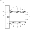
- Electromagnetic Wave Detector 102 is a schematic cross-sectional view of an electromagnetic wave detector 102 according to embodiment 3. As shown in FIG. 6, the electromagnetic wave detector 102 further includes a first tunnel insulating layer 61 and a second tunnel insulating layer 62. The first tunnel insulating layer 61 is sandwiched between the first two-dimensional material layer 11 and the first semiconductor layer 41. The second tunnel insulating layer 62 is sandwiched between the second two-dimensional material layer 12 and the second semiconductor layer 42.
- the first tunnel insulating layer 61 is disposed inside the first opening 31A of the first insulating layer 31.
- the second tunnel insulating layer 62 is disposed inside the second opening 32A of the second insulating layer 32.
- the thicknesses of the first tunnel insulating layer 61 and the second tunnel insulating layer 62 are set so that when electromagnetic waves to be detected are incident on the electromagnetic wave detector 102, tunnel currents are generated between the first two-dimensional material layer 11 and the first semiconductor layer 41 and between the second two-dimensional material layer 12 and the second semiconductor layer 42.
- the thicknesses of the first tunnel insulating layer 61 and the second tunnel insulating layer 62 are, for example, 1 nm or more and 10 nm or less.
- each of the first tunnel insulating layer 61 and the second tunnel insulating layer 62 may be any material having electrical insulation properties, and may include at least one selected from the group consisting of metal oxides such as alumina and hafnium oxide, or oxides containing semiconductors such as silicon oxide and silicon nitride, and nitrides such as boron nitride. Any method can be used as a method for manufacturing each of the first tunnel insulating layer 61 and the second tunnel insulating layer 62.
- Each of the first tunnel insulating layer 61 and the second tunnel insulating layer 62 can be manufactured using, for example, an ALD (Atomic Layer Deposition) method, a vacuum deposition method, a sputtering method, or the like.
- Each of the first tunnel insulating layer 61 and the second tunnel insulating layer 62 can also be formed by oxidizing or nitriding the first surface 41A of the first semiconductor layer 41 or the second surface 42A of the second semiconductor layer 42.
- Each of the first tunnel insulating layer 61 and the second tunnel insulating layer 62 may be a natural oxide film.
- the electromagnetic wave detector 102 may further include at least one of a first tunnel insulating layer 61 and a second tunnel insulating layer 62.
- the configuration of the electromagnetic wave detector in this embodiment can also be applied to other embodiments.
- the electromagnetic wave detector 102 includes the first tunnel insulating layer 61 disposed between the first two-dimensional material layer 11 and the first semiconductor layer 41, leakage current at the junction interface between the first semiconductor layer 41 and the first two-dimensional material layer 11 can be suppressed and dark current can be reduced. Furthermore, since the electromagnetic wave detector 102 further includes the second tunnel insulating layer 62 disposed between the second two-dimensional material layer 12 and the second semiconductor layer 42, leakage current at the junction interface between the second semiconductor layer 42 and the second two-dimensional material layer 12 can be suppressed and dark current can be reduced.
- each of the first tunnel insulating layer 61 and the second tunnel insulating layer 62 is set so that, when electromagnetic waves to be detected are incident on the electromagnetic wave detector 102, tunnel currents are generated between the first two-dimensional material layer 11 and the first semiconductor layer 41 and between the second two-dimensional material layer 12 and the second semiconductor layer 42. In this way, when electromagnetic waves to be detected are incident on the electromagnetic wave detector 102, a relatively large photocurrent can flow between the first semiconductor layer 41 and the first two-dimensional material layer 11 and between the second semiconductor layer 42 and the second two-dimensional material layer 12, thereby increasing the sensitivity of the electromagnetic wave detector 102.
- Embodiment 4 Unless otherwise specified, the electromagnetic wave detector according to the embodiment 4 has the same configuration, operating principle, and effects as those of the above-mentioned embodiment 1. Therefore, the same components as those of the above-mentioned embodiment 1 are given the same reference numerals, and the description thereof will not be repeated.
- the first connecting conductor 71 forms a Schottky junction with the first semiconductor layer 41.
- the second connecting conductor 72 forms a Schottky junction with the second semiconductor layer 42.
- the thickness of the first connecting conductor 71 may be equal to the thickness of the first insulating layer 31.
- the first two-dimensional material layer 11 extends in a planar manner from the upper surface of the first insulating layer 31 to above the upper surface of the first connecting conductor 71 without bending.
- the thickness of the second connecting conductor 72 may be equal to the thickness of the second insulating layer 32.
- the second two-dimensional material layer 12 extends in a planar manner from the upper surface of the second insulating layer 32 to above the upper surface of the second connecting conductor 72 without bending.
- the configuration of the electromagnetic wave detector in this embodiment can also be applied to other embodiments.
- the first semiconductor layer 41 and the first two-dimensional material layer 11 are electrically connected via the first connecting conductor 71, so that the contact resistance between the first two-dimensional material layer 11 and the first semiconductor layer 41 can be reduced compared to a case in which the first connecting conductor 71 is not provided.
- the dark current can be reduced.
- the thickness of the first connecting conductor 71 is equivalent to the thickness of the first insulating layer 31, the two-dimensional surfaces of the first portion 11a and the third portion 11c of the first two-dimensional material layer 11 extend in the same direction, improving the mobility of carriers in the first two-dimensional material layer 11.
- the optical gate effect on the first two-dimensional material layer 11 is proportional to the mobility of carriers in the first two-dimensional material layer 11. Therefore, the detection sensitivity of the electromagnetic wave detector 103 can be improved compared to that of the electromagnetic wave detector 100.
- Embodiment 5 Unless otherwise specified, the electromagnetic wave detector according to the embodiment 5 has the same configuration, operating principle, and effects as those of the above-mentioned embodiment 1. Therefore, the same components as those of the above-mentioned embodiment 1 are given the same reference numerals, and the description thereof will not be repeated.
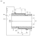
- Fig. 8 is a schematic plan view of an electromagnetic wave detector 104 according to the fifth embodiment.
- Fig. 9 is a schematic cross-sectional view seen from the arrow IX-IX in Fig. 8.
- a plurality of uneven portions 81, 82 are formed on the surface of each of the first electrode 21 and the second electrode 22.
- Each of the plurality of uneven portions 81, 82 constitutes a pattern in which surface plasmons are excited resonantly when an electromagnetic wave to be detected is incident thereon.
- a pattern in which surface plasmons are excited resonantly when an electromagnetic wave to be detected is incident thereon is provided on the surface of each of the first electrode 21 and the second electrode 22.
- the multiple uneven portions 81 formed on the surface of the first electrode 21 are formed, for example, by the first electrode 21 and multiple conductors arranged at intervals on the upper surface of the first electrode 21.
- the multiple uneven portions 82 formed on the surface of the second electrode 22 are formed, for example, by the second electrode 22 and multiple conductors arranged at intervals on the upper surface of the second electrode 22.
- the material constituting the conductor is a material that generates surface plasmon resonance.
- the material constituting the conductor includes at least one selected from the group consisting of gold (Au), silver (Ag), copper (Cu), aluminum (Al), nickel (Ni), chromium (Cr), and palladium (Pd).
- the method for forming the multiple uneven portions 81, 82 is not particularly limited, but may be formed in the same manner as the first electrode 21 and the second electrode 22, for example.
- the multiple uneven portions 81, 82 may be formed by partially removing the first electrode 21 or the second electrode 22 by dry etching, wet etching, or the like.
- the multiple uneven portions 81, 82 are formed as a pattern 80 in which surface plasmon resonance occurs on each surface of the first electrode 21 or the second electrode 22.
- the multiple uneven portions 81, 82 have, for example, a one-dimensional periodic structure or a two-dimensional periodic structure.
- the one-dimensional periodic structure or the two-dimensional periodic structure of the multiple uneven portions 81, 82 is a periodic structure along the two-dimensional surface of the first two-dimensional material layer 11 or the second two-dimensional material layer 12.
- the multiple uneven portions 81, 82 having a one-dimensional periodic structure are periodically arranged, for example, in any direction along the two-dimensional surface of each of the first two-dimensional material layer 11 and the second two-dimensional material layer 12.
- the multiple uneven portions 81, 82 having a two-dimensional periodic structure are arranged, for example, in a plan view, at positions corresponding to lattice points of a square lattice, a triangular lattice, or the like.
- the multiple uneven portions 81, 82 may have a non-periodic structure.
- the arrangement of the multiple uneven portions 81, 82 in a plan view may be asymmetric.
- the planar shape of the convex portions of the multiple uneven portions 81, 82 may be any shape, such as a circle, a triangle, a square, a polygon, or an ellipse.
- a pattern that resonantly excites surface plasmons when electromagnetic waves to be detected are incident on at least one of the surfaces of the first electrode 21, the first two-dimensional material layer 11, the second electrode 22, and the second two-dimensional material layer 12 may be provided.
- a plurality of uneven portions may be provided on at least one of the surfaces of the first electrode 21, the first two-dimensional material layer 11, the second electrode 22, and the second two-dimensional material layer 12. In a plan view, the plurality of uneven portions may have a periodic structure or a non-periodic structure.
- a plurality of uneven portions 91, 92 may be formed on the surface of each of the first two-dimensional material layer 11 and the second two-dimensional material layer 12.
- Each of the plurality of uneven portions 91, 92 constitutes a pattern in which surface plasmons are resonantly excited when electromagnetic waves to be detected are incident thereon.
- a pattern is provided on the surface of each of the first two-dimensional material layer 11 and the second two-dimensional material layer 12 in which surface plasmons are resonantly excited when electromagnetic waves to be detected are incident thereon.
- the multiple uneven portions 91 are formed, for example, by the first two-dimensional material layer 11 and multiple conductors arranged at intervals on the upper surface of the first two-dimensional material layer 11.
- the multiple uneven portions 92 are formed, for example, by the second two-dimensional material layer 12 and multiple conductors arranged at intervals on the upper surface of the second two-dimensional material layer 12.
- Each of the multiple conductors is in contact with the upper surface of the first two-dimensional material layer 11 or the second two-dimensional material layer 12.
- Each of the multiple conductors is in contact, for example, with the third portion 11c of the first two-dimensional material layer 11 or the sixth portion 12c of the second two-dimensional material layer 12.
- At least one of the first two-dimensional material layer 11 and the second two-dimensional material layer 12 may have a plurality of recesses or protrusions, and the plurality of recesses or protrusions may constitute a plurality of uneven portions 91, 92. Since each of the first two-dimensional material layer 11 and the second two-dimensional material layer 12 has a high electrical conductivity, surface plasmon resonance may occur in each of the first two-dimensional material layer 11 and the second two-dimensional material layer 12.
- the plurality of uneven portions 91, 92 constituted by a plurality of recesses or protrusions may also cause surface plasmon resonance in each of the first two-dimensional material layer 11 and the second two-dimensional material layer 12.
- the electromagnetic wave detector 104 a plurality of uneven portions may be formed on the surface of each of the first electrode 21, the first two-dimensional material layer 11, the second electrode 22, and the second two-dimensional material layer 12.
- the electromagnetic wave detector 104 may have a plurality of uneven portions 81, 82 and a plurality of uneven portions 91, 92 formed simultaneously.
- ⁇ Effects of the electromagnetic wave detector 104 a pattern is provided on the surface of at least any one of the first electrode 21, the first two-dimensional material layer 11, the second electrode 22, and the second two-dimensional material layer 12, such that, when an electromagnetic wave to be detected is incident thereon, the surface plasmon is resonantly excited. Therefore, in the electromagnetic wave detector 104, only the electromagnetic wave to be detected is incident on the light receiving element 40, thereby increasing the detection sensitivity for the electromagnetic wave to be detected.
- the multiple uneven portions 81, 82, 91, 92 have a one-dimensional periodic structure, only electromagnetic waves having a polarization that generates surface plasmon resonance can be detected, and the detection sensitivity to the electromagnetic waves is increased. If the multiple uneven portions 81, 82, 91, 92 have a two-dimensional periodic structure, only electromagnetic waves having a wavelength that generates surface plasmon resonance can be detected, and the detection sensitivity to the electromagnetic waves is increased.
- Embodiment 6 Unless otherwise specified, the electromagnetic wave detector according to the embodiment 6 has the same configuration, operating principle, and effects as those of the above-mentioned embodiment 1. Therefore, the same components as those of the above-mentioned embodiment 1 are given the same reference numerals, and the description thereof will not be repeated.
- Fig. 12 is a schematic plan view of an electromagnetic wave detector 105 according to embodiment 6.
- Fig. 13 is a schematic cross-sectional view seen from the arrow XIII-XIII in Fig. 12.
- the area of the first electrode 21 is smaller than the area of the first opening 31A in a plan view.
- the ratio of the area of the first electrode 21 to the area of the first surface 41A is, for example, 0.3 or less.
- the ratio of the area of the first electrode 21 to the area of the first surface 41A is, for example, 0.1 or less.
- the area of the second electrode 22 is smaller than the area of the second opening 32A.
- the ratio of the area of the second electrode 22 to the area of the second surface 42A is, for example, 0.3 or less.
- the ratio of the area of the second electrode 22 to the area of the second surface 42A is, for example, 0.1 or less.
- the configuration of the electromagnetic wave detector in this embodiment can also be applied to other embodiments.
- the area of the first electrode 21 is smaller than the area of the first opening 31A, and therefore the amount of light that passes through the first surface 41A and reaches the second surface 42A is increased compared to when the area of the first electrode 21 is equal to or greater than the area of the first opening 31A, resulting in an increased output.
- Embodiment 7 Unless otherwise specified, the electromagnetic wave detector according to the embodiment 7 has the same configuration, operating principle, and effects as those of the above-mentioned embodiment 1. Therefore, the same components as those of the above-mentioned embodiment 1 are given the same reference numerals, and the description thereof will not be repeated.
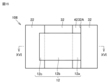
- FIG. 14 is a schematic plan view of the electromagnetic wave detector 106 according to the seventh embodiment.
- FIG. 15 is a schematic bottom view of the electromagnetic wave detector 106 according to the seventh embodiment.
- FIG. 16 is a schematic cross-sectional view seen from the arrows XVI-XVI in FIG. 14 and FIG. 15.
- the area of the second electrode 22 is larger than the area of the first electrode 21 in a plan view.
- the area of the second electrode 22 is, for example, twice or more the area of the first electrode 21.
- the area of the first electrode 21 is, for example, smaller than the area of the first opening 31A.
- the area of the second electrode 22 is, for example, equal to or larger than the area of the second opening 32A.
- the configuration of the electromagnetic wave detector in this embodiment can also be applied to other embodiments.
- the area of the second electrode 22 is larger than the area of the first electrode 21, so that the electromagnetic wave that is incident on the light receiving element 40 from the first surface 41A side and transmitted through the light receiving element 40 is reflected by the second electrode 22.
- the electromagnetic wave reflected by the second electrode 22 is incident on the light receiving element 40 again from the second surface 42A side. Therefore, the electromagnetic wave is incident on the light receiving element 40 from both the first surface 41A and the second surface 42A sides. This increases the electromagnetic wave absorption rate of the light receiving element 40, and therefore increases the output.
- Embodiment 8 Unless otherwise specified, the electromagnetic wave detector according to the embodiment 8 has the same configuration, operating principle, and effects as those of the above-mentioned embodiment 1. Therefore, the same components as those of the above-mentioned embodiment 1 are given the same reference numerals, and the description thereof will not be repeated.
- FIG. 17 is a schematic plan view of an electromagnetic wave detector 107 according to the eighth embodiment.
- the electromagnetic wave detector 107 does not have symmetry with the interface between the third surface 41B and the fourth surface 42B as the mirror plane.
- a portion located on the first semiconductor layer 41 side with respect to the interface does not have a mirror-symmetric relationship with a portion located on the second semiconductor layer 42 side with respect to the interface.
- the first portion 11a of the first two-dimensional material layer 11 is arranged so as not to overlap with the fourth portion 12a of the second two-dimensional material layer 12.
- the first opening 31A is arranged so as not to overlap with the second opening 32A.
- the first electrode 21 is arranged so as not to overlap with the second electrode 22.
- the configuration of the electromagnetic wave detector in this embodiment can also be applied to other embodiments.
- Fig. 18 is a schematic plan view of an electromagnetic wave detector array according to the ninth embodiment.
- Fig. 19 is a schematic plan view showing a modified example of the electromagnetic wave detector according to the ninth embodiment.
- the electromagnetic wave detector array 200 shown in FIG. 18 is an electromagnetic wave detector assembly, and includes a plurality of electromagnetic wave detectors 300 as detection elements.
- Each of the plurality of electromagnetic wave detectors 300 is any one of the electromagnetic wave detectors 100 to 107 of embodiments 1 to 8.
- each of the electromagnetic wave detectors 300 may be the electromagnetic wave detector 100.
- each of the plurality of electromagnetic wave detectors 300 is arranged in an array in a two-dimensional direction. Note that each of the plurality of electromagnetic wave detectors 300 may be arranged so as to be aligned in a one-dimensional direction.
- the electromagnetic wave detector array 200 includes four electromagnetic wave detectors 300, which are arranged in a 2 x 2 array.
- the electromagnetic wave detector array 200 may include any number of electromagnetic wave detectors 300, and may include, for example, nine or more electromagnetic wave detectors 300.
- the multiple electromagnetic wave detectors 100 may be arranged in an array of 3 or more x 3 or more.
- the multiple electromagnetic wave detectors 300 may be arranged non-periodically.
- each of the multiple electromagnetic wave detectors 300 may be common to each other, so long as each of the multiple electromagnetic wave detectors 300 can function as a single detection element.
- Each of the multiple electromagnetic wave detectors 300 forms, for example, one pixel in the electromagnetic wave detector array 200.
- the electromagnetic wave detector array 200 can be used, for example, as an image sensor in which each of the multiple electromagnetic wave detectors 300 forms one pixel.
- Each of the multiple electromagnetic wave detectors 300 may be an electromagnetic wave detector according to an embodiment other than the electromagnetic wave detector 100 according to embodiment 1.
- the electromagnetic wave detector array 201 shown in FIG. 19 basically has the same configuration as the electromagnetic wave detector array 200 shown in FIG. 18 and can achieve the same effects, but differs from the electromagnetic wave detector array 200 in that it has multiple electromagnetic wave detectors 300, 301, 302, and 303 with different configurations.
- Each of the multiple electromagnetic wave detectors 300, 301, 302, and 303 is any one of the electromagnetic wave detectors 100 to 107 of embodiments 1 to 8.
- the electromagnetic wave detector 300 may be the electromagnetic wave detector 100
- the electromagnetic wave detector 301 may be the electromagnetic wave detector 101
- the electromagnetic wave detector 302 may be the electromagnetic wave detector 102
- the electromagnetic wave detector 303 may be the electromagnetic wave detector 103.
- electromagnetic wave detector array 201 In the electromagnetic wave detector array 201 shown in FIG. 19, multiple different types of electromagnetic wave detectors 300, 301, 302, and 303 are arranged in a one-dimensional or two-dimensional array, allowing the array to function as an image sensor.
- electromagnetic wave detectors 300, 301, 302, and 303 may each have a different detection wavelength.
- electromagnetic wave detectors having different detection wavelength selectivities may be prepared from the electromagnetic wave detectors according to any of the first to eighth embodiments, and these may be arranged in an array. In this case, the electromagnetic wave detector array 201 can detect electromagnetic waves of at least two or more different wavelengths.
- the electromagnetic wave detectors 300, 301, 302, and 303 having different detection wavelengths in an array it is possible to distinguish the wavelength of electromagnetic waves in any wavelength range, such as ultraviolet light, infrared light, terahertz waves, and radio wave wavelength ranges, in the same way as image sensors used in the visible light range. As a result, it is possible to obtain a colored image in which differences in wavelength are shown as differences in color, for example.
- the material constituting at least one of the first semiconductor layer 41 and the second semiconductor layer 42 of each of the multiple types of electromagnetic wave detectors 300, 301, 302, and 303 may be a material having sensitivity in different wavelength ranges.
- the material constituting the first semiconductor layer 41 of the electromagnetic wave detector 300 may be a semiconductor material whose detection wavelength is the wavelength of visible light
- the material constituting the first semiconductor layer 41 of the electromagnetic wave detector 301 may be a semiconductor material whose detection wavelength is the wavelength of infrared light.
- Such an electromagnetic wave detector array 201 is suitable for, for example, an in-vehicle sensor.
- Such an electromagnetic wave detector array 201 can function as an image sensor for a visible light image camera during the day and as an image sensor for an infrared camera at night. Therefore, a camera equipped with the above-mentioned electromagnetic wave detector array 201 as an image sensor does not need to be used according to the detection wavelength.
- the electromagnetic wave detector array 201 which includes multiple electromagnetic wave detectors 300, 301, 302, and 303 having different detection wavelengths, can be used as an image sensor that can detect multiple electromagnetic waves having different wavelengths. This makes it possible to detect multiple electromagnetic waves having different wavelengths without using color filters that were previously required for CMOS (Complementary MOS) sensors and the like. It is also possible to obtain a colorized image in which differences in the wavelengths of the electromagnetic waves are shown as differences in color.
- CMOS Complementary MOS
- a polarization discrimination image sensor can be formed by arraying electromagnetic wave detectors 300, 301, 302, and 303 that detect different polarizations. For example, four pixels that detect polarization angles of 0°, 90°, 45°, and 135° are treated as one unit, and multiple electromagnetic wave detectors of this unit are arranged to enable polarization imaging.
- the polarization discrimination image sensor makes it possible, for example, to distinguish between man-made and natural objects, to distinguish between materials, to distinguish between objects of the same temperature in the infrared wavelength range, to distinguish between boundaries between objects, or to improve equivalent resolution.
- the arrangement of the multiple electromagnetic wave detectors 300, 301, 302, and 303 is not particularly limited.
- the multiple electromagnetic wave detectors 300, 301, 302, and 303 can be arranged periodically or non-periodically.
- the electromagnetic wave detector assembly according to this embodiment configured as described above, can detect electromagnetic waves in a wide wavelength range.
- the electromagnetic wave detector assembly according to this embodiment can detect electromagnetic waves of different wavelengths.
Landscapes
- Light Receiving Elements (AREA)
Priority Applications (2)
| Application Number | Priority Date | Filing Date | Title |
|---|---|---|---|
| JP2024543362A JP7562054B1 (ja) | 2023-12-20 | 2023-12-20 | 電磁波検出器及び電磁波検出器アレイ |
| PCT/JP2023/045632 WO2025134255A1 (ja) | 2023-12-20 | 2023-12-20 | 電磁波検出器及び電磁波検出器アレイ |
Applications Claiming Priority (1)
| Application Number | Priority Date | Filing Date | Title |
|---|---|---|---|
| PCT/JP2023/045632 WO2025134255A1 (ja) | 2023-12-20 | 2023-12-20 | 電磁波検出器及び電磁波検出器アレイ |
Publications (1)
| Publication Number | Publication Date |
|---|---|
| WO2025134255A1 true WO2025134255A1 (ja) | 2025-06-26 |
Family
ID=92909814
Family Applications (1)
| Application Number | Title | Priority Date | Filing Date |
|---|---|---|---|
| PCT/JP2023/045632 Pending WO2025134255A1 (ja) | 2023-12-20 | 2023-12-20 | 電磁波検出器及び電磁波検出器アレイ |
Country Status (2)
| Country | Link |
|---|---|
| JP (1) | JP7562054B1 (https=) |
| WO (1) | WO2025134255A1 (https=) |
Families Citing this family (1)
| Publication number | Priority date | Publication date | Assignee | Title |
|---|---|---|---|---|
| CN120035233B (zh) * | 2025-02-24 | 2025-11-25 | 中国科学院上海技术物理研究所 | 一种外尔半金属长波红外探测器及其制备方法 |
Citations (3)
| Publication number | Priority date | Publication date | Assignee | Title |
|---|---|---|---|---|
| US20170256667A1 (en) * | 2016-03-02 | 2017-09-07 | Gwangju Institute Of Science And Technology | Graphene-semiconductor schottky junction photodetector of having tunable gain |
| WO2021002070A1 (ja) * | 2019-07-04 | 2021-01-07 | 三菱電機株式会社 | 電磁波検出器 |
| WO2021124609A1 (ja) * | 2019-12-17 | 2021-06-24 | 三菱電機株式会社 | 電磁波検出器および電磁波検出器集合体 |
-
2023
- 2023-12-20 WO PCT/JP2023/045632 patent/WO2025134255A1/ja active Pending
- 2023-12-20 JP JP2024543362A patent/JP7562054B1/ja active Active
Patent Citations (3)
| Publication number | Priority date | Publication date | Assignee | Title |
|---|---|---|---|---|
| US20170256667A1 (en) * | 2016-03-02 | 2017-09-07 | Gwangju Institute Of Science And Technology | Graphene-semiconductor schottky junction photodetector of having tunable gain |
| WO2021002070A1 (ja) * | 2019-07-04 | 2021-01-07 | 三菱電機株式会社 | 電磁波検出器 |
| WO2021124609A1 (ja) * | 2019-12-17 | 2021-06-24 | 三菱電機株式会社 | 電磁波検出器および電磁波検出器集合体 |
Also Published As
| Publication number | Publication date |
|---|---|
| JPWO2025134255A1 (https=) | 2025-06-26 |
| JP7562054B1 (ja) | 2024-10-04 |
Similar Documents
| Publication | Publication Date | Title |
|---|---|---|
| US10784394B2 (en) | Electromagnetic wave detector and electromagnetic wave detector array | |
| US11682741B2 (en) | Electromagnetic wave detector | |
| JP7499857B2 (ja) | 電磁波検出器および電磁波検出器集合体 | |
| JP7550854B2 (ja) | 電磁波検出器および電磁波検出器アレイ | |
| JP7345593B2 (ja) | 電磁波検出器および電磁波検出器アレイ | |
| JP7433533B1 (ja) | 電磁波検出器および電磁波検出器アレイ | |
| JP7374222B2 (ja) | 電磁波検出器および電磁波検出器集合体 | |
| JP7422963B1 (ja) | 電磁波検出器 | |
| JP7399361B2 (ja) | 電磁波検出器及び電磁波検出器アレイ | |
| JP7403670B2 (ja) | 電磁波検出器および電磁波検出器アレイ | |
| JP7740896B2 (ja) | 電磁波検出器および電磁波検出器集合体 | |
| JP7562054B1 (ja) | 電磁波検出器及び電磁波検出器アレイ | |
| WO2023112770A1 (ja) | 電磁波検出器及び電磁波検出器アレイ | |
| JP7728489B1 (ja) | 電磁波検出器 | |
| WO2024100784A1 (ja) | 電磁波検出器および電磁波検出器集合体 |
Legal Events
| Date | Code | Title | Description |
|---|---|---|---|
| ENP | Entry into the national phase |
Ref document number: 2024543362 Country of ref document: JP Kind code of ref document: A |
|
| WWE | Wipo information: entry into national phase |
Ref document number: 2024543362 Country of ref document: JP |