WO2025121069A1 - 高周波信号伝送線路及び電子機器 - Google Patents
高周波信号伝送線路及び電子機器 Download PDFInfo
- Publication number
- WO2025121069A1 WO2025121069A1 PCT/JP2024/039618 JP2024039618W WO2025121069A1 WO 2025121069 A1 WO2025121069 A1 WO 2025121069A1 JP 2024039618 W JP2024039618 W JP 2024039618W WO 2025121069 A1 WO2025121069 A1 WO 2025121069A1
- Authority
- WO
- WIPO (PCT)
- Prior art keywords
- resin
- resin layer
- transmission line
- frequency signal
- signal transmission
- Prior art date
- Legal status (The legal status is an assumption and is not a legal conclusion. Google has not performed a legal analysis and makes no representation as to the accuracy of the status listed.)
- Pending
Links
Images









Classifications
-
- H—ELECTRICITY
- H01—ELECTRIC ELEMENTS
- H01P—WAVEGUIDES; RESONATORS, LINES, OR OTHER DEVICES OF THE WAVEGUIDE TYPE
- H01P3/00—Waveguides; Transmission lines of the waveguide type
- H01P3/02—Waveguides; Transmission lines of the waveguide type with two longitudinal conductors
- H01P3/08—Microstrips; Strip lines
-
- H—ELECTRICITY
- H05—ELECTRIC TECHNIQUES NOT OTHERWISE PROVIDED FOR
- H05K—PRINTED CIRCUITS; CASINGS OR CONSTRUCTIONAL DETAILS OF ELECTRIC APPARATUS; MANUFACTURE OF ASSEMBLAGES OF ELECTRICAL COMPONENTS
- H05K1/00—Printed circuits
- H05K1/02—Details
Definitions
- the present invention relates to a high-frequency signal transmission line and an electronic device equipped with the same.
- Patent Document 1 shows a transmission line with a suspended structure in which a signal line is formed in a resin layer and hollow parts are formed above and below this signal line.
- the side of the adhesive layer that contacts the hollow part is configured to have a concave shape.
- the adhesive layer is in contact only with the top and bottom surfaces of the base layer, so in a structure that forms a hollow section, the adhesive strength of the laminate is weak.
- the strength of the upper and lower layers of the hollow section is weak. Therefore, when the vicinity of the hollow section of the high-frequency signal transmission line is deformed by an external force applied to the high-frequency signal transmission line, the electrical characteristics of the high-frequency signal transmission line become unstable.
- the object of the present invention is to provide a high-frequency signal transmission line that maintains high strength in the resin laminate and hollow portion and has stable electrical characteristics, and an electronic device equipped with the same.
- a resin laminated section in which a single or multiple first resin layers and a single or multiple second resin layers are laminated, a signal conductor pattern arranged to be in contact with at least one of the single or multiple first resin layers, and a ground conductor layer facing the signal conductor pattern with a part or all of the resin laminated section in between; an opening is formed in at least one of the first resin layers at a position along the signal conductor pattern in the resin laminate portion, so that a hollow portion is provided in the resin laminate portion at the opening;
- the second resin layer in contact with the first resin layer in which the opening is formed is characterized in that the second resin layer in contact with the first resin layer is adhered to a portion of an end face at the opening of the first resin layer in which the opening is formed.
- the present invention provides a high-frequency signal transmission line with high resistance to external stress and stable electrical characteristics, and an electronic device equipped with the same.
- FIG. 1 The upper part of FIG. 1 is a plan view of a high-frequency signal transmission line 101 according to the first embodiment, and the lower part of FIG. 1 is a vertical cross-sectional view of a portion enclosed by a dashed dotted line in the upper part of FIG.
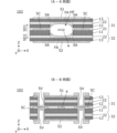
- FIG. 2 is a plan view of the high-frequency signal transmission line 102 according to the second embodiment.
- 3 is a vertical cross-sectional view taken along dashed line AA in FIG. 2
- the lower part of FIG. 3 is a vertical cross-sectional view taken along dashed line BB in FIG. 4A to 4C are plan views of the layers in the middle of the manufacturing process of the high-frequency signal transmission line 102.
- FIG. 1 The upper part of FIG. 1 is a plan view of a high-frequency signal transmission line 101 according to the first embodiment
- the lower part of FIG. 1 is a vertical cross-sectional view of a portion enclosed by a dashed dotted line in the upper part of FIG.
- FIG. 2 is
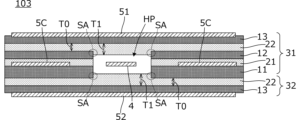
- FIG. 5 is a cross-sectional view of a high-frequency signal transmission line 103 according to the third embodiment.
- FIG. 6 is a cross-sectional view of a high-frequency signal transmission line 104 according to the fourth embodiment.
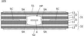
- FIG. 7 is a cross-sectional view of a high-frequency signal transmission line 105 according to the fifth embodiment.
- FIG. 8 is a cross-sectional view of a high-frequency signal transmission line 106 according to the sixth embodiment.
- FIG. 9 is a cross-sectional view of a high-frequency signal transmission line 107 according to the seventh embodiment.
- the upper part of FIG. 10 is a plan view of the high-frequency signal transmission line 108 according to the eighth embodiment, and the lower part of FIG.
- FIG. 10 is a vertical cross-sectional view of the dashed line portion in the upper part of FIG.
- the upper part of FIG. 11 is a plan view of the high-frequency signal transmission line 109 according to the ninth embodiment
- the lower part of FIG. 11 is a vertical cross-sectional view of the dashed line portion in the upper part of FIG.
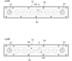
- FIG. 12 is a plan view of high-frequency signal transmission lines 110A and 110B according to the tenth preferred embodiment.
- FIG. 13 is a plan view of the first resin layer 11 of four types of high-frequency signal transmission lines according to the eleventh embodiment.
- FIG. 14 is a plan view of the first resin layer 11 of two types of high-frequency signal transmission lines according to the eleventh embodiment.
- FIG. 15 is a cross-sectional view of the high-frequency signal transmission line 112 according to the twelfth embodiment of the present invention.
- the lower part of Fig. 15 is a cross-sectional view of the high-frequency signal transmission line 112 showing the electric field distribution caused by electric force lines.
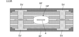
- FIG. 16 is a vertical sectional view of a high-frequency signal transmission line 113A according to the thirteenth preferred embodiment.
- FIG. 17 is a vertical cross-sectional view of a high-frequency signal transmission line 113B according to the thirteenth preferred embodiment.
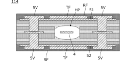
- FIG. 18 is a vertical sectional view of a high-frequency signal transmission line 114 according to a fourteenth preferred embodiment of the present invention.
- FIG. 1 The upper part of FIG. 1 is a plan view of a high-frequency signal transmission line 101 according to the first embodiment, and the lower part of FIG. 1 is a vertical cross-sectional view of the dashed line portion in the upper part of FIG. 1.
- a single high-frequency signal transmission line 101 is shown in FIG. 1, a large number of high-frequency signal transmission lines that are continuous in the planar direction are manufactured up to the final process during manufacturing, and are separated into each high-frequency signal transmission line in the final process. This is the same for each of the embodiments shown below.
- This high-frequency signal transmission line 101 includes a resin laminate portion 3, a signal conductor pattern 4, and a ground conductor layer 5.
- the resin laminate section 3 is a section where the first resin layers 11, 12, 13 and the second resin layers 21, 22 are laminated.
- the signal conductor pattern 4 is formed on the upper surface of the first resin layer 11.
- the ground conductor layer 5 is laminated on the upper surface of the first resin layer 13. In other words, the signal conductor pattern 4 and the ground conductor layer 5 face each other with a part of the resin laminate section 3 in between.
- a circular opening is formed in the first resin layer 12 and the second resin layer 21.
- this opening is circular when viewed in the stacking direction of the first resin layers 11, 12, 13 and the second resin layers 21, 22.
- an opening is formed in the first resin layer 12 at a position along the signal conductor pattern 4 in the resin laminate portion 3, and a hollow portion HP is provided in the resin laminate portion 3 at this opening.
- a hollow portion HP is formed in which the first resin layer 12 and the second resin layer 22 do not contact the signal conductor pattern 4.
- stacking direction does not refer to the direction of the stacking order of the layers during manufacturing, but rather to the direction of stacking of the layers in the state shown in the figure.
- this high-frequency signal transmission line 101 has six hollow portions HP.
- the signal conductor pattern 4 passes through the hollow portions HP at six points.
- This high-frequency signal transmission line 101 acts as a microstrip line consisting of the signal conductor pattern 4, the ground conductor layer 5, a part of the resin laminate portion 3, and the hollow portions HP.
- the periodic change in characteristic impedance due to the change in the relative dielectric constant around the signal conductor pattern 4 does not pose a problem.
- a signal conductor pattern terminal 4T which is separated from the ground conductor layer 5, is formed on the upper surface of the resin laminate portion 3.
- the end of the signal conductor pattern 4 is connected to the signal conductor pattern terminal 4T via an interlayer connection conductor.
- a coaxial connector 61 is mounted on the upper signal conductor pattern terminal 4T, and a coaxial connector 62 is mounted on the lower signal conductor pattern terminal 4T.
- the high-frequency signal transmission line 101 is used as a transmission line with coaxial connectors on both ends.
- the coaxial connectors 61 and 62 in Figure 1 show their mounting positions.
- the signal conductor pattern 4 and the ground conductor layer 5 are both, for example, copper foil.
- the material of the first resin layers 11, 12, and 13 is, for example, polyimide, liquid crystal polymer, or epoxy resin.
- the material of the second resin layers 21 and 22 is, for example, thermoplastic polyimide, fluorine-based resin, or polyolefin-based resin. Polyolefin-based resins are, for example, styrene, polyethylene, and polypropylene.
- the second resin layers 21 and 22 act as adhesive layers that bond adjacent first resin layers of the first resin layers 11, 12, and 13 together.
- the flexibility of the second resin layers 21 and 22 at room temperature is greater than the flexibility of the first resin layers 11, 12, and 13 at room temperature.
- room temperature is, for example, 25°C or room temperature.
- the Young's modulus of the second resin layers 21 and 22 is 1 MPa or less, and the Young's modulus of the first resin layers 11, 12, and 13 is 2 MPa or more.
- the second resin layers 21, 22 have high fluidity during processing. They may flow and harden after bonding a portion of the end face (inner end face) of the opening. Possible materials for the second resin layers 21, 22 include, for example, prepreg materials used for interlayer bonding.
- the second resin layer has a lower dielectric constant than the first resin layer.
- the second resin layers 21 and 22 have a dielectric constant of 2.2 to 2.8
- the first resin layers 11, 12, and 13 have a dielectric constant of 2.8 to 4.0.
- the dielectric tangent of the second resin layer is lower than the dielectric tangent of the first resin layer.
- the dielectric tangent of the second resin layers 21 and 22 is 0.0005 to 0.003
- the dielectric tangent of the first resin layers 11, 12, and 13 is 0.002 to 0.01.
- either the high/low relationship of the relative dielectric constant or the high/low relationship of the dielectric tangent may satisfy the above relationship.
- the second resin layer 22 in contact with the first resin layer 12 in which the opening is formed has a different maximum thickness and minimum thickness at the opening formed in the first resin layer 12, so that the second resin layer 22 is adhered to a part of the end face (inner end face) of the opening of the first resin layer 12 in which the opening is formed.
- the second resin layer 22 is adhered to a part of the end face (inner side face) of the opening of the first resin layer 12, forming an adhesive portion SA.
- the portion of the second resin layer that forms part of the hollow portion is a curved surface that expands outward from the hollow portion HP near the center of the hollow portion HP compared to the periphery of the hollow portion HP.
- the curved surface forms an elliptical arc.
- the cross section of the curved surface is a circular arc.
- the second resin layer 22 has a curved surface that expands outward from the hollow portion near the center compared to the periphery of the hollow portion, but the first resin layer 13 and the second resin layer 22 are bonded together over their entire surfaces. In other words, the first resin layer 13 is not exposed inside the hollow portion HP.
- the portion FA shown at the bottom of Figure 1 indicates the adhesive portion where the second resin layer 22 is adhered to the first resin layer 13, even though the film thickness of the second resin layer 22 is thinner than the adhesive portion SA.
- the strength of the hollow portion HP is high, the stress applied from the outside to the high-frequency signal transmission line 101 is mitigated, and damage such as peeling between the layers is prevented.
- the portion of the resin laminate 3 that forms part of the hollow portion HP is a curved surface that expands outward from the hollow portion HP near the center compared to the periphery of the hollow portion HP, so the air layer near the signal conductor pattern 4 is thicker. As a result, both the dielectric tangent and the dielectric constant of the dielectric between the signal conductor pattern 4 and the ground conductor layer 5 are small, and the dielectric loss of the high-frequency signal transmission line is reduced.
- the portion that forms part of the hollow portion is not the relatively less flexible first resin layer, but the relatively more flexible second resin layer, which is a curved surface that extends outward from the periphery of the hollow portion near the center. Therefore, the stress applied from the outside to the high-frequency signal transmission line 101 is effectively mitigated by the second resin layer, and the reduction in strength due to the presence of the hollow portion HP is suppressed.
- the second resin layer 22 has a curved surface that expands outward from the hollow portion HP near the center compared to the periphery of the hollow portion HP, and the first resin layer 13 and the second resin layer 22 are bonded to each other over their entire surfaces, so that the adhesive strength between the first resin layer 13 and the second resin layer 22 is high. Therefore, the strength of the hollow portion HP is high, and the stress applied to the high-frequency signal transmission line 101 from the outside is mitigated, preventing damage.
- the signal conductor pattern 4 is exposed in the hollow portion HP, but the signal conductor pattern 4 may also be formed on the underside of the first resin layer 11 (the surface opposite to the surface on which the hollow portion HP is formed). In this case, it is easier to ensure the distance between the ground conductor layer 5 and the signal conductor pattern 4. Therefore, the line width of the signal conductor pattern can be made thicker to obtain a predetermined characteristic impedance, which can also reduce transmission loss.
- FIG. 2 is a plan view of a high-frequency signal transmission line 102 according to the second embodiment.
- the upper part of FIG. 3 is a vertical cross-sectional view of the dashed line A-A in FIG. 2, and the lower part of FIG. 3 is a vertical cross-sectional view of the dashed line B-B in FIG. 2.
- This high-frequency signal transmission line 102 includes an upper resin laminate portion 31, a lower resin laminate portion 32, a signal conductor pattern 4, a first ground conductor layer 51, a second ground conductor layer 52, a ground conductor pattern 5C, and an interlayer connection conductor 5V.
- the upper resin laminate portion 31 is a portion where the upper first resin layers 11, 12, 13 and the second resin layers 21, 22 are laminated.
- the lower resin laminate portion 32 is a portion where the lower first resin layer 13 and the lower second resin layer 22 are laminated. That is, the resin laminate portion is composed of the upper resin laminate portion 31 laminated in a first lamination direction SD1 of the lamination directions of the first resin layer and the second resin layer, and the lower resin laminate portion 32 configured in a second lamination direction SD2, which is the opposite direction to the first lamination direction SD1.
- the signal conductor pattern 4 and the ground conductor pattern 5C are formed on the upper surface of the first resin layer 11.
- a first ground conductor layer 51 is laminated on the upper surface of the upper first resin layer 13.
- a second ground conductor layer 52 is laminated on the lower surface of the lower first resin layer 13.
- the signal conductor pattern 4 faces the first ground conductor layer 51 and the second ground conductor layer 52, with the upper resin laminate portion 31 and the lower resin laminate portion 32 sandwiched between them.
- interlayer connection conductors 5V are formed in the upper resin laminate part 31. These interlayer connection conductors 5V electrically connect the first ground conductor layer 51 and the ground conductor pattern 5C. In addition, interlayer connection conductors 5V are formed in the lower resin laminate part 32. These interlayer connection conductors 5V electrically connect the second ground conductor layer 52 and the ground conductor pattern 5C.
- Circular openings are formed in the first resin layers 11, 12 and the second resin layer 21. In terms of the shape shown in the drawing, these openings are circular when viewed in the stacking direction of the first resin layers 11, 12, 13 and the second resin layers 21, 22.
- an opening is formed in the first resin layer 12 at a position along the signal conductor pattern 4 in the upper resin laminate portion 31, and this opening provides a hollow portion HP around the signal conductor pattern 4.
- a hollow portion HP is formed in which the first resin layers 11, 12 and the second resin layers 21, 22 do not contact the signal conductor pattern 4.
- this high-frequency signal transmission line 102 has six hollow portions HP.
- the signal conductor pattern 4 passes through the hollow portions HP at six points.
- This high-frequency signal transmission line 102 acts as a strip line consisting of the signal conductor pattern 4, the first ground conductor layer 51, the second ground conductor layer 52, the upper resin laminate portion 31, the lower resin laminate portion 32, and the hollow portions HP.
- the spacing between the hollow portions HP is less than 1/4 wavelength of the transmission signal, the periodic change in the characteristic impedance due to the change in the relative dielectric constant around the signal conductor pattern 4 does not pose a problem.
- the signal conductor pattern 4, the first ground conductor layer 51, and the second ground conductor layer 52 are all, for example, copper foil.
- the material of the first resin layers 11, 12, and 13 is, for example, polyimide, liquid crystal polymer, or epoxy resin.
- the material of the second resin layers 21 and 22 is, for example, thermoplastic polyimide, fluorine-based resin, or polyolefin-based resin.
- the polyolefin-based resin is, for example, styrene, polyethylene, or polypropylene.
- the second resin layers 21 and 22 act as an adhesive layer that bonds adjacent first resin layers of the first resin layers 11, 12, and 13 together.
- the relationship between the flexibility of the second resin layers 21, 22 and the first resin layers 11, 12, 13, the relationship between the relative dielectric constant of the second resin layers 21, 22 and the first resin layers 11, 12, 13, and the relationship between the dielectric tangent of the second resin layers 21, 22 and the first resin layers 11, 12, 13 are the same as those in the example shown in the first embodiment.
- the portion indicated by the dashed line at the top of the figure is the adhesive portion SA where the upper second resin layer 22 is adhered to a portion of the end face (inner surface) of the opening of the first resin layer 12.
- the portion FA indicated by the dashed line at the top of the figure shows the adhesive portion where the upper second resin layer 22 is adhered to the upper first resin layer 13 even though the film thickness of the upper second resin layer 22 is thinner than the original thickness.
- the portion indicated by the dashed line at the bottom of the figure is an adhesive portion SA where the lower second resin layer 22 is adhered to a portion of the end face (inner surface) of the opening of the first resin layer 11.
- portion FA indicated by the dashed line at the bottom of the figure shows the adhesive portion where the film thickness of the lower second resin layer 22 has become thinner than the original thickness, but is still adhered to the lower first resin layer 13.
- FIG. 4 is a plan view of each layer during the manufacturing process of the high-frequency signal transmission line 102.
- the high-frequency signal transmission line 102 includes, from the top, the first resin layer 13, the second resin layer 22, the first resin layer 12, the second resin layer 21, the first resin layer 11, the second resin layer 22, and the first resin layer 13.
- the first resin layers 11, 12, and the second resin layer 21 have circular openings OH.
- the upper second resin layer 22 melts and extends to the end face (inner surface) of the opening of the first resin layer 12.
- the lower second resin layer 22 melts and extends to the end face (inner surface) of the opening of the first resin layer 11.
- the hollow portion HP formed by the overlapping openings OH expands due to heating. That is, the film thickness of the upper second resin layer 22 becomes thinner than the original thickness of the upper second resin layer 22, and the film thickness of the lower second resin layer 22 becomes thinner than the original thickness of the lower second resin layer 22, so that the hollow portion HP expands in the stacking direction.
- the interlayer connection conductor 5V shown in Figure 3 is formed by forming an opening that exposes the ground conductor pattern 5C from the outer surface of the laminate formed by laminating the above-mentioned resin layers using laser processing, and then depositing a copper plating film inside this opening.
- This embodiment provides the same effects as those described in the first embodiment. In addition, this embodiment provides the following effects:
- the interlayer connection conductors 5V are arranged on both sides of the arrangement line of the hollow sections HP, and the midpoint of the arrangement pitch of the hollow sections HP coincides with the arrangement position of the interlayer connection conductors 5V, so that the strength of the laminate formed by stacking each resin layer is evenly increased by the interlayer connection conductors 5V.
- the second resin layers 21 and 22 are more flexible than the first resin layers 11, 12, and 13, so that the second resin layers 21 and 22 can absorb the steps of the ground conductor pattern 5C and wrap around the inner surface of the hollow portion HP in a stable shape. Incidentally, if the flexibility of each resin layer is equal (if the first resin layers 11, 12, and 13 and the second resin layers 21 and 22 are both soft), it would be difficult to maintain a stable shape of the hollow portion HP.
- FIG. 5 is a cross-sectional view of a high-frequency signal transmission line 103 according to the third embodiment.
- This high-frequency signal transmission line 103 includes an upper resin laminate portion 31, a lower resin laminate portion 32, a signal conductor pattern 4, a first ground conductor layer 51, a second ground conductor layer 52, a ground conductor pattern 5C, and an interlayer connection conductor (for example, the interlayer connection conductor 5V shown in FIG. 3).
- the upper resin laminated portion 31 is a portion where the upper first resin layers 11, 12, 13 and the lower second resin layers 21, 22 are laminated.
- the lower resin laminated portion 32 is a portion where the lower first resin layer 13 and the lower second resin layer 22 are laminated.
- the signal conductor pattern 4 and the ground conductor pattern 5C are formed on the upper surface of the first resin layer 11.
- a first ground conductor layer 51 is laminated on the upper surface of the upper first resin layer 13.
- a second ground conductor layer 52 is laminated on the lower surface of the lower first resin layer 13.
- the signal conductor pattern 4 faces the first ground conductor layer 51 and the second ground conductor layer 52, with the upper resin laminate portion 31 and the lower resin laminate portion 32 sandwiched between them.
- Circular openings are formed in the first resin layers 11, 12 and the second resin layer 21. In terms of the shape shown in the drawing, these openings are circular when viewed in the stacking direction of the first resin layers 11, 12, 13 and the second resin layers 21, 22.
- an opening is formed in the first resin layers 11, 12 at a position along the signal conductor pattern 4, and this opening provides a hollow portion HP around the signal conductor pattern 4.
- the upper second resin layer 22 in contact with the first resin layer 12 in which the opening is formed protrudes into the opening of the first resin layer 12, and in the region of the opening of the first resin layer 12, the thickness T1 of the upper second resin layer 22 is thicker than the thickness T0 of the other region.
- the lower second resin layer 22 in contact with the first resin layer 11 in which the opening is formed protrudes into the opening of the first resin layer 11, and in the region of the opening of the first resin layer 11, the thickness T1 of the lower second resin layer 22 is thicker than the thickness T0 of the other region.
- the upper second resin layer 22 is adhered to a portion of the end face (inner end face) of the opening of the first resin layer 12 in which the opening is formed.
- the lower second resin layer 22 is adhered to a portion of the end face (inner end face) of the opening of the first resin layer 11 in which the opening is formed.
- the adhesion strength between the upper second resin layer 22 and the first resin layer 12, and the adhesion strength between the lower second resin layer 22 and the first resin layer 11 are high. Therefore, the strength of the hollow portion HP is high, and external stress applied to the high-frequency signal transmission line 101 is alleviated, preventing damage.
- the second resin layers 22 above and below the hollow portion HP are thick and flat, the strength of the hollow portion HP can be easily increased. The cross-sectional shape of this hollow portion HP can be changed depending on the flexibility of the second resin layer 22, etc.
- FIG. 6 is a cross-sectional view of a high-frequency signal transmission line 104 according to the fourth embodiment.
- This high-frequency signal transmission line 104 includes an upper resin laminate portion 31, a lower resin laminate portion 32, a signal conductor pattern 4, a first ground conductor layer 51, a second ground conductor layer 52, and a ground conductor pattern 5C.
- the ground conductor pattern 5C is an intermediate layer ground conductor pattern that provides electrical conduction with the first ground conductor layer 51 and the second ground conductor layer 52 via the interlayer connection conductor.
- the difference from the high-frequency signal transmission line 102 shown in the upper part of Figure 3 is that there is a non-adhesive portion NA between the upper second resin layer 22 and the upper first resin layer 13, and there is a non-adhesive portion NA between the lower second resin layer 22 and the lower first resin layer 13.
- the air layers above and below the signal conductor pattern 4 can be made thicker than in the high-frequency signal transmission line shown in the second embodiment, and dielectric loss can be reduced more effectively.
- non-adhesive portions NA are formed on both the top and bottom of the signal conductor pattern 4, but non-adhesive portions NA may be formed only on either the top or bottom.
- the high-frequency signal transmission line 104 of this embodiment is manufactured by the following method.
- the upper second resin layer 22 when applying the upper second resin layer 22 to the upper first resin layer 13, it is applied except for the position facing the opening of the first resin layer 12.
- the lower second resin layer 22 when applying the lower second resin layer 22 to the lower first resin layer 13, it is applied except for the position facing the opening of the first resin layer 11.
- the upper second resin layer 22 is applied to the entire surface of the upper first resin layer 13, and then the area near the position facing the opening of the first resin layer 12 is partially removed.
- the lower second resin layer 22 is applied to the entire surface of the lower first resin layer 13, and then the area near the position facing the opening of the first resin layer 11 is partially removed.
- the height of the hollow portion HP can be easily increased.
- FIG. 7 is a cross-sectional view of a high-frequency signal transmission line 105 according to the fifth embodiment.
- This high-frequency signal transmission line 105 includes an upper resin laminate portion 31, a lower resin laminate portion 32, a signal conductor pattern 4, a first ground conductor layer 51, a second ground conductor layer 52, and a ground conductor pattern 5C.
- the ground conductor pattern 5C is an intermediate layer ground conductor pattern that provides electrical conduction with the first ground conductor layer 51 and the second ground conductor layer 52 via the interlayer connection conductor.
- the second resin layer 21, which is an adhesive layer, and the upper second resin layer 22 are bonded to the entire end face (inner surface) of the opening of the first resin layer 12 in the thickness direction, so the adhesion strength between these second resin layers 21, 22 and the first resin layer 12 is high. Therefore, the strength of the hollow portion HP is more effectively increased.
- FIG. 6 An example of a suspended line type high-frequency signal transmission line is shown in which a hollow portion HP exists above a signal conductor pattern 4 and another hollow portion HP exists below a first resin layer 11 in which the signal conductor pattern is formed.
- FIG. 8 is a cross-sectional view of a high-frequency signal transmission line 106 according to the sixth embodiment.
- This high-frequency signal transmission line 106 includes an upper resin laminate portion 31, a lower resin laminate portion 32, a signal conductor pattern 4, a first ground conductor layer 51, a second ground conductor layer 52, and a ground conductor pattern 5C.
- the upper resin laminate portion 31 is a portion where the upper first resin layers 11, 12, 13 and the second resin layers 21, 22 are laminated.
- the lower resin laminate portion 32 is a portion where the lower first resin layers 12, 13 and the lower second resin layers 22, 23 are laminated. That is, the resin laminate portion is composed of the upper resin laminate portion 31 laminated in a first lamination direction SD1 of the lamination directions of the first resin layers and the second resin layers, and the lower resin laminate portion 32 configured in a second lamination direction SD2 that is the opposite direction to the first lamination direction SD1.
- the signal conductor pattern 4 and the ground conductor pattern 5C are formed on the upper surface of the first resin layer 11.
- a first ground conductor layer 51 is laminated on the upper surface of the upper first resin layer 13.
- a second ground conductor layer 52 is laminated on the lower surface of the lower first resin layer 13.
- Circular openings are formed in the upper first resin layer 12 and the lower second resin layer 21. Also, circular openings are formed in the lower first resin layer 12 and the lower second resin layer 22.
- the rest of the structure is the same as the high-frequency signal transmission line shown in the second embodiment.
- the presence of the first resin layer 11 that continuously supports the signal conductor pattern 4 makes it easy to increase the strength of the signal conductor pattern 4.
- the seventh embodiment shows an example of a high-frequency signal transmission line in which the shape of hollow portions HP formed above and below a signal conductor pattern 4 is different from that shown in the sixth embodiment.
- FIG. 9 is a cross-sectional view of a high-frequency signal transmission line 107 according to the seventh embodiment.
- This high-frequency signal transmission line 107 includes an upper resin laminate portion 31, a lower resin laminate portion 32, a signal conductor pattern 4, a first ground conductor layer 51, a second ground conductor layer 52, and a ground conductor pattern 5C.
- the rest of the structure is the same as the high-frequency signal transmission line shown in the sixth embodiment.
- the upper adhesive portion SA in FIG. 9 represents that portion.
- the lower adhesive portion SA in FIG. 9 indicates that portion.
- the side surfaces of the other first resin layers adjacent to the first resin layer on which the signal conductor pattern 4 is formed are also bonded with the second resin layer, so the strength of the hollow portion HP is high, and external stress applied to the high-frequency signal transmission line 107 is mitigated, preventing damage.
- FIG. 10 The upper part of FIG. 10 is a plan view of the high-frequency signal transmission line 108 according to the eighth embodiment, and the lower part of FIG. 10 is a vertical cross-sectional view of the dashed line portion in the upper part of FIG. 10.
- This high-frequency signal transmission line 108 includes an upper resin laminate portion 31, a lower resin laminate portion 32, a signal conductor pattern 4, a first ground conductor layer 51, a second ground conductor layer 52, a ground conductor pattern 5C, and an interlayer connection conductor 5V.
- the upper resin laminated portion 31 is a portion where the upper first resin layers 11, 12, 13 and the lower second resin layers 21, 22 are laminated.
- the lower resin laminated portion 32 is a portion where the lower first resin layer 13 and the lower second resin layer 22 are laminated.
- the signal conductor pattern 4 and the ground conductor pattern 5C are formed on the upper surface of the first resin layer 11.
- a first ground conductor layer 51 is laminated on the upper surface of the upper first resin layer 13.
- a second ground conductor layer 52 is laminated on the lower surface of the lower first resin layer 13.
- the signal conductor pattern 4 faces the first ground conductor layer 51 and the second ground conductor layer 52, with the upper resin laminate portion 31 and the lower resin laminate portion 32 sandwiched between them.
- Interlayer connection conductors 5V are formed in the upper resin laminate portion 31. These interlayer connection conductors 5V electrically connect the first ground conductor layer 51 and the ground conductor pattern 5C. In addition, interlayer connection conductors 5V are formed in the lower resin laminate portion 32. These interlayer connection conductors 5V electrically connect the second ground conductor layer 52 and the ground conductor pattern 5C.
- this high-frequency signal transmission line 10 does not have multiple hollow portions HP as shown in the upper part of FIG. 1, for example, but has a continuous hollow portion HP along the extension direction of the signal conductor pattern 4.
- This high-frequency signal transmission line 108 acts as a strip line consisting of the signal conductor pattern 4, the first ground conductor layer 51, the second ground conductor layer 52, the first resin layer, the second resin layer, and the hollow portion HP.
- the hollow portion HP is only formed in the upper resin layer, the mechanical strength of the signal conductor pattern 4 is easily maintained high even if stress is applied near the hollow portion HP due to an external force on the high-frequency signal transmission line 108.
- the hollow portion HP is not dispersed in the signal propagation direction, no periodic change in the characteristic impedance occurs.
- FIG. 11 The upper part of FIG. 11 is a plan view of the high-frequency signal transmission line 109 according to the ninth embodiment, and the lower part of FIG. 11 is a vertical cross-sectional view of the dashed line portion in the upper part of FIG. 11.
- This high-frequency signal transmission line 109 includes an upper resin laminate portion 31, a lower resin laminate portion 32, a signal conductor pattern 4, a first ground conductor layer 51, a second ground conductor layer 52, a ground conductor pattern 5C, and an interlayer connection conductor 5V.
- the interlayer connection conductor 5V is formed by forming a conductor plating film on the inner surface of the opening formed in each resin layer between the first ground conductor layer 51 and the ground conductor pattern 5C, and similarly, the interlayer connection conductor 5V is formed by forming a conductor plating film on the inner surface of the opening formed in each resin layer between the second ground conductor layer 52 and the ground conductor pattern 5C.
- the interlayer connection conductor 5V is formed by filling the opening formed in each resin layer between the first ground conductor layer 51 and the ground conductor pattern 5C with a conductor
- the interlayer connection conductor 5V is formed by filling the opening formed in each resin layer between the second ground conductor layer 52 and the ground conductor pattern 5C with a conductor.
- FIG. 2 an example is shown in which the interlayer connection conductors 5V are arranged on both sides of the arrangement line of the hollow portions HP when viewed in the layering direction of each resin, and the midpoint of the arrangement pitch of the hollow portions HP coincides with the arrangement position of the interlayer connection conductors 5V.
- the interlayer connection conductors 5V are arranged on both sides of the hollow portions HP when viewed in the layering direction of each resin.
- the strength of the hollow portion HP is effectively increased by the interlayer connection conductors 5V. That is, when viewed in the stacking direction of the resin layers, the interlayer connection conductors 5V adjacent to the hollow portion HP are positioned to straddle the hollow portion HP, so that the interlayer connection conductors 5V are located in the vicinity of the hollow portion HP. This allows the strength of the hollow portion HP to be effectively increased by the interlayer connection conductors 5V.
- the interlayer connection conductor 5V protrudes from the surface and is positioned to span the hollow portion, even if an object comes into contact with it from the outside (even if it comes into contact with an external object), the object will hit the protruding part of the interlayer connection conductor 5V, preventing it from hitting the top or bottom of the hollow portion HP, thereby suppressing deformation of the hollow portion HP.
- the example shown in FIG. 2 also satisfies the structure in which the interlayer connection conductors 5V adjacent to the hollow portion HP are positioned to straddle the hollow portion HP.
- the interlayer connection conductors 5V adjacent to the hollow portion HP straddle the hollow portion HP on a line inclined at 45 degrees to the arrangement direction of the hollow portion HP.
- FIG. 12 is a plan view of high-frequency signal transmission lines 110A and 110B according to the tenth embodiment.
- Both of the high-frequency signal transmission lines 110A and 110B include a first ground conductor layer 51, a ground conductor pattern 51C, a signal conductor pattern terminal 4T, multiple hollow portions HP, and multiple interlayer connection conductors 5V.
- the internal structure is as shown in the second embodiment.
- the second ground conductor layer 52 overlaps with the first ground conductor layer 51 in the plan view.
- the arrangement of the interlayer connection conductors 5V is different between the high-frequency signal transmission lines 110A and 110B. Both the high-frequency signal transmission lines 110A and 110B have fewer interlayer connection conductors than the examples shown in Figures 2 and 11.
- adjacent interlayer connection conductors 5V are positioned so that they sandwich the hollow portion HP in the plan view, and pass through (straddle) the same hollow portion HP.
- adjacent interlayer connection conductors 5V are positioned so that they sandwich the hollow portion HP in the plan view, and pass through (straddle) the two hollow portions HP.
- interlayer connection conductors 5V Even if the number of such interlayer connection conductors 5V is small, if adjacent interlayer connection conductors 5V are positioned so as to sandwich the hollow portion HP in a plan view and pass through (straddle) the hollow portion HP, the interlayer connection conductors 5V will provide a high degree of reinforcement for the hollow portion HP, reducing the stress applied from the outside to the high-frequency signal transmission lines 110A, 110B and preventing damage.
- (1) in FIG. 13 is a plan view of the first resin layer 11 of an example of a high-frequency signal transmission line.
- it is a plan view of the first resin layer 11 of the high-frequency signal transmission line 102 shown in the second embodiment.
- (2) and (3) in FIG. 13 are plan views of the first resin layer 11 (the first resin layer in which the signal conductor pattern 4 is formed) of a high-frequency signal transmission line whose hollow portion shape and their arrangement pitch are different from those of the example in (1).
- (4) in FIG. 13 is a plan view of the first resin layer 11 of a high-frequency signal transmission line whose signal conductor pattern line width in the hollow portion and other portions is different.
- a number of circular openings OH are formed in the first resin layer 11.
- the width of these openings OH is AW
- the spacing between the openings OH is GS.
- the larger the value of AW/GS the higher the rate at which the signal conductor pattern 4 passes through the hollow portion, and the dielectric loss due to the relative dielectric constant and dielectric tangent of the resin layer is reduced.
- the value of AW/GS becomes extremely large, the strength of the hollow portion created by the openings OH becomes lower than the specified value, and there is a risk of damage near the hollow portion.
- oval openings OH are formed in the first resin layer 11.
- the width of these openings OH is AW
- the spacing between the openings OH is GS.
- the larger the value of AW/GS the higher the rate at which the signal conductor pattern 4 passes through the hollow portion, and the dielectric loss due to the relative dielectric constant and dielectric tangent of the resin layer is reduced.
- the major axis of the openings OH is aligned with the extension direction of the signal conductor pattern 4, the efficiency of lengthening the openings OH relative to the expansion of the planar area of the openings OH is high. Therefore, even if the value of AW/GS is not extremely large, the dielectric loss can be effectively reduced, and the strength of the hollow portion formed by the openings OH can be maintained, reducing the risk of damage near the hollow portion.
- the gap GS can be lengthened, and the strength of the hollow portion can be maintained.
- openings OH are formed in the first resin layer 11 in the shape of two overlapping circles shifted by a certain distance in the extension direction of the signal conductor pattern 4.
- the width of these openings OH in the extension direction of the signal conductor pattern 4 is AW, and the spacing between the openings OH is GS.
- the long axis of the opening OH is aligned with the extension direction of the signal conductor pattern 4, so that the efficiency of lengthening the opening OH relative to the expansion of the planar area of the opening OH is high.
- the efficiency of lengthening the opening OH relative to the expansion of the planar area of the opening OH is higher. Therefore, the rate of expansion of the planar area accompanying an increase in the value of AW/GS is suppressed. This maintains the strength of the hollow portion formed by the opening OH, and further reduces the risk of damage near the hollow portion.
- the line width of the signal conductor pattern 4 differs between the portion laminated on the second resin layer (second resin layer 21 shown in FIG. 3) and the portion not in contact with the second resin layer.
- the line width of the signal conductor pattern 4 not in contact with the second resin layer is wider than the line width of the signal conductor pattern 4 laminated on the second resin layer.
- the diagram shown in the upper part of Figure 14 is a plan view of the first resin layer 11 of an example of a high-frequency signal transmission line.
- the lower part of Figure 14 is a plan view of the first resin layer 11 (the first resin layer in which the signal conductor pattern 4 is formed) of a high-frequency signal transmission line in which the shape of the hollow portions and their arrangement pitch are different from those of the example in the upper part.
- multiple diamond-shaped openings OH with rounded corners are formed in the first resin layer 11.
- the width of these openings OH in the extension direction of the signal conductor pattern 4 is AW
- the spacing between the openings OH in the extension direction of the signal conductor pattern 4 is GS.
- the larger the value of AW/GS the higher the rate at which the signal conductor pattern 4 passes through the hollow portion, thereby reducing the dielectric loss due to the relative dielectric constant and dielectric tangent of the resin layer.
- openings OH in the shape of three diamonds overlapping each other and shifted by a certain distance in the extension direction of the signal conductor pattern 4 are formed in the first resin layer 11.
- the width of these openings OH in the extension direction of the signal conductor pattern 4 is AW, and the spacing between the openings OH is GS.
- the major axis of the openings OH is aligned with the extension direction of the signal conductor pattern 4, so that the efficiency of lengthening the openings OH relative to the expansion of the planar area of the openings OH is high.
- Twelfth embodiment In the twelfth embodiment, a high-frequency signal transmission line in which the top and bottom of a resin laminate are recessed will be illustrated.
- FIG. 15 The upper part of FIG. 15 is a cross-sectional view of the high-frequency signal transmission line 112 according to this embodiment.
- the lower part of FIG. 15 is a cross-sectional view of the high-frequency signal transmission line 112, showing the electric field distribution caused by electric field lines.
- This high-frequency signal transmission line 112 includes an upper resin laminate portion 31, a lower resin laminate portion 32, a signal conductor pattern 4, a first ground conductor layer 51, a second ground conductor layer 52, and a ground conductor pattern 5C.
- the rest of the basic structure is similar to that of the high-frequency signal transmission line 109 shown in FIG. 11.
- the high-frequency signal transmission line 112 of this embodiment has a recess RA that is recessed at the top and bottom of the hollow portion HP in the resin lamination direction. During manufacturing, the high-frequency signal transmission line 112 is pressed with the first ground conductor layer 51 attached to the first resin layer 13 to form the recess RA.
- the high-frequency signal transmission line 112 of this embodiment provides the following effects:
- the resin layer near the hollow portion HP has an arch-shaped cross section, which effectively suppresses deformation of the hollow portion HP and its surroundings.
- the arrows protruding from the signal conductor pattern 4 at the bottom of FIG. 15 are noteworthy electric field lines.
- an electric field is generated between the signal conductor pattern 4 and the first ground conductor layer 51, and between the signal conductor pattern 4 and the second ground conductor layer 52.
- the current density in the signal conductor pattern 4 increases toward both ends.
- the electric field strength is suppressed toward both ends of the signal conductor pattern 4, so the current distribution in the signal conductor pattern 4 is averaged. As a result, the conductor loss due to the signal conductor pattern 4 is mitigated.
- FIG. 16 is a vertical cross-sectional view of a high-frequency signal transmission line 113A constructed by forming a resist film on the high-frequency signal transmission line 109 shown in FIG. 11.
- FIG. 17 is a vertical cross-sectional view of a high-frequency signal transmission line 113B formed by forming a resist film on the high-frequency signal transmission line 109 shown in FIG. 11.
- the resist film RF shown in Figures 16 and 17 is a resist film formed by applying a resist resin to the front and back of the high-frequency signal transmission line 109 shown in Figure 11 and then hardening it.
- the resist film RF on the outer surface, the stress applied from the outside to the high frequency signal transmission lines 113A and 113B is alleviated by the resist film RF, and the reduction in strength of the high frequency signal transmission lines due to the presence of the hollow portion HP is further suppressed.
- FIG. 18 is a vertical cross-sectional view of a high-frequency signal transmission line 114 according to a fourteenth embodiment.
- the plating thickness of the first ground conductor layer 51 and the second ground conductor layer 52 in the area that overlaps with the hollow portion HP is increased to form a thickened portion TF.
- the plating of this area may be performed simultaneously with the plating for forming the interlayer connection conductor 5V.
- the strength of the hollow portion HP in the laminate above and below is effectively increased. This makes it possible to more effectively suppress deformation of the hollow portion HP.
- the high-frequency signal transmission line of the present invention can be used as a high-frequency signal transmission line in various electronic devices.
- connectors are provided on the high-frequency circuits formed on two circuit boards, and the coaxial connectors 61 and 62 of the high-frequency signal transmission line 101 shown in Figure 1 are connected to each other.
- the circuit boards and high-frequency signal transmission line 101 are housed in a housing of a specified shape. In this way, an electronic device is constructed.
- a high-frequency signal transmission line having a single signal conductor pattern is shown, but it may have multiple signal conductor patterns.
- a differential line may be configured with two or more signal conductor patterns. This can also be applied to a configuration in which the multiple signal conductor patterns that make up this differential line are arranged within a single hollow portion.
- multiple signal conductor patterns may be arranged in the layer direction of each resin layer, or in the stacking direction of each resin layer.
- a rectangular high-frequency signal transmission line is shown when viewed from the stacking direction of each resin layer, but this shape is arbitrary.
- a high-frequency signal transmission line having a linear signal conductor pattern is shown, but when viewed from the stacking direction of each resin layer, the signal conductor pattern may be curved or partially curved.
- each resin layer may be a curved surface such as a cylindrical surface, or a partially curved surface. Also, for example, the entire surface or a portion of the surface may be a twisted curved surface.
- a separate resin layer different from the first resin layer and the second resin layer may be provided to bond the copper foil forming the ground conductor layer to the first resin layer.
- the high-frequency signal transmission line and electronic device of the present invention may be provided in the following forms.
- a resin laminated section in which a single or multiple first resin layers and a single or multiple second resin layers are laminated, a signal conductor pattern arranged to be in contact with at least one of the single or multiple first resin layers, and a ground conductor layer facing the signal conductor pattern with a part or all of the resin laminated section in between; an opening is formed in at least one of the first resin layers at a position along the signal conductor pattern in the resin laminate portion, so that a hollow portion is provided in the resin laminate portion at the opening; the second resin layer in contact with the first resin layer in which the opening is formed is bonded to a part of an end surface of the first resin layer in which the opening is formed, at the opening; High frequency signal transmission line.
- the ground conductor layer is composed of a first ground layer and a second ground conductor layer that are present on both sides of the signal conductor pattern in the lamination direction, the first resin layer and the second resin layer are present on both sides of the signal conductor pattern in the lamination direction,
- ⁇ 3> an interlayer connection conductor electrically connecting the first ground conductor layer and the second ground conductor layer; a transmission line is formed by the first ground conductor layer, the second ground conductor layer, the upper resin laminate portion, the lower resin laminate portion, the signal conductor pattern, and the interlayer connection conductor; The high-frequency signal transmission line according to ⁇ 2>.
- the interlayer connection conductor has a protruding portion protruding outward in the first stacking direction from the first ground conductor layer, and the interlayer connection conductor has a protruding portion protruding outward in the second stacking direction from the second ground conductor layer.
- ⁇ 5> a third resin layer covering the protruding portion of the interlayer connection conductor on an outer surface of the upper resin laminate portion or the lower resin laminate portion;
- the second resin layer in contact with the first resin layer in which the opening is formed has a maximum thickness and a minimum thickness different from each other at the opening formed in the first resin layer, so that the second resin layer in contact with the first resin layer is bonded to a part of an end surface at the opening of the first resin layer in which the opening is formed.
- a portion of the second resin layer that forms a part of the hollow portion has a curved surface that expands outward from the hollow portion near the center compared to the periphery of the hollow portion.
- the high-frequency signal transmission line according to any one of ⁇ 1> to ⁇ 6>.
- the second resin layer has greater flexibility than the first resin layer.
- the high-frequency signal transmission line according to any one of ⁇ 1> to ⁇ 7>.
- the resin material of the second resin layer has a lower dielectric constant and a lower dielectric tangent than the resin material of the first resin layer.
- the high-frequency signal transmission line according to any one of ⁇ 1> to ⁇ 8>.
- a part of the second resin layer is formed in an arch shape at the opening of the first resin layer.
- the high-frequency signal transmission line according to any one of ⁇ 1> to ⁇ 9>.
- the opening of the second resin layer is formed in the opening of the first resin layer, and the opening of the first resin layer and the opening of the second resin layer form the hollow portion.
- ⁇ 13> The hollow portion is formed over a wider area than the width of the signal conductor pattern.
- ⁇ 13> The high-frequency signal transmission line according to any one of ⁇ 1> to ⁇ 12>.
- ⁇ 14> An electronic device comprising the high-frequency signal transmission line according to any one of ⁇ 1> to ⁇ 13>.
Landscapes
- Engineering & Computer Science (AREA)
- Microelectronics & Electronic Packaging (AREA)
- Waveguides (AREA)
Abstract
高周波信号伝送線路(102)は、第1樹脂層(11,12,13)及び第2樹脂層(21,22)が積層された樹脂積層部と、第1樹脂層(11)に形成された信号導体パターン(4)と、樹脂積層部を挟んで信号導体パターンに対向するグランド導体層(51,52)と、を備える。樹脂積層部のうち、信号導体パターン(4)に沿った位置の第1樹脂層(11,12)に開口部が形成されていることにより、これら開口部で樹脂積層部に中空部(HP)が設けられている。開口部が形成された第1樹脂層(11,12)に接する第2樹脂層(22)は、第1樹脂層に形成された開口部において最大厚みと最小厚みとが異なることにより、第1樹脂層(11,12)の開口部における端面の一部に第1樹脂層に接する第2樹脂層が接着している。
Description
本発明は、高周波信号伝送線路及びそれを備える電子機器に関する。
特許文献1には、樹脂層に信号線が形成され、この信号線の上下に中空部が形成された、サスペンディッド構造の伝送線路が示されている。また、中空部に接する接着層の側面が凹形状になるように構成されている。
特許文献1に記載の高周波信号伝送線路では、接着層が基材層の上下面だけにしか接していないため、中空部を形成するという構造では、積層体の接着強度が弱い。また、中空部の上下に接着層が存在しないため、中空部の上下層の強度が弱い。そのため、高周波信号伝送線路に対する外力によって高周波信号伝送線路の中空部近傍が変形すると、高周波信号伝送線路の電気的特性が不安定となる。
そこで、本発明の目的は、樹脂積層部及び中空部の強度を高く保持し、電気的特性の安定した高周波信号伝送線路及びそれを備える電子機器を提供することにある。
本開示の一例としての高周波信号伝送線路は、
単一又は複数の第1樹脂層及び単一又は複数の第2樹脂層が積層された樹脂積層部と、前記単一又は複数の第1樹脂層のうち少なくとも単一の第1樹脂層に接するように配置された信号導体パターンと、前記樹脂積層部の一部又は全部を挟んで前記信号導体パターンに対向するグランド導体層と、を備え、
前記樹脂積層部のうち、前記信号導体パターンに沿った位置の前記第1樹脂層のうち少なくとも単一の前記第1樹脂層に開口部が形成されていることにより、前記開口部で前記樹脂積層部に中空部が設けられ、
前記開口部が形成された前記第1樹脂層に接する前記第2樹脂層は、前記開口部が形成された前記第1樹脂層の前記開口部における端面の一部に、前記第1樹脂層に接する前記第2樹脂層が接着している、ことを特徴とする。
単一又は複数の第1樹脂層及び単一又は複数の第2樹脂層が積層された樹脂積層部と、前記単一又は複数の第1樹脂層のうち少なくとも単一の第1樹脂層に接するように配置された信号導体パターンと、前記樹脂積層部の一部又は全部を挟んで前記信号導体パターンに対向するグランド導体層と、を備え、
前記樹脂積層部のうち、前記信号導体パターンに沿った位置の前記第1樹脂層のうち少なくとも単一の前記第1樹脂層に開口部が形成されていることにより、前記開口部で前記樹脂積層部に中空部が設けられ、
前記開口部が形成された前記第1樹脂層に接する前記第2樹脂層は、前記開口部が形成された前記第1樹脂層の前記開口部における端面の一部に、前記第1樹脂層に接する前記第2樹脂層が接着している、ことを特徴とする。
本発明によれば、外部から加わる応力に対する耐性が高く、電気的特性の安定した高周波信号伝送線路及びそれを備える電子機器が得られる。
以降、図を参照して幾つかの具体的な例を挙げて、本発明を実施するための複数の形態を示す。各図中には同一箇所に同一符号を付している。要点の説明又は理解の容易性を考慮して、実施形態を説明の便宜上、複数の実施形態に分けて示すが、異なる実施形態で示した構成の部分的な置換又は組み合わせは可能である。第2の実施形態以降では第1の実施形態と共通の事柄についての記述を省略し、異なる点についてのみ説明する。特に、同様の構成による同様の作用効果については実施形態毎には逐次言及しない。
《第1の実施形態》
第1の実施形態ではマイクロストリップ線路タイプの高周波信号伝送線路の一例について示す。
第1の実施形態ではマイクロストリップ線路タイプの高周波信号伝送線路の一例について示す。
図1の上部は第1の実施形態に係る高周波信号伝送線路101の平面図であり、図1の下部は、図1の上部における一点鎖線部分の縦断面図である。図1においては単一の高周波信号伝送線路101について示しているが、製造時の最終工程までは、面方向に連続する多数の高周波信号伝送線路を製造し、最終工程で各高周波信号伝送線路に分離する。このことは、以降に示す各実施形態においても同様である。
この高周波信号伝送線路101は、樹脂積層部3と、信号導体パターン4と、グランド導体層5と、を備える。
樹脂積層部3は、第1樹脂層11,12,13及び第2樹脂層21,22が積層された部分である。信号導体パターン4は第1樹脂層11の上面に形成されている。第1樹脂層13の上面にはグランド導体層5が積層されている。すなわち、樹脂積層部3の一部を挟んで信号導体パターン4とグランド導体層5とは対向している。
第1樹脂層12及び第2樹脂層21には円形の開口が形成されている。図面上の形状で表せば、この開口は、第1樹脂層11,12,13及び第2樹脂層21,22の積層方向に視て円形である。
このように、樹脂積層部3のうち、信号導体パターン4に沿った位置の第1樹脂層12に開口部が形成されていることにより、この開口部で樹脂積層部3に中空部HPが設けられている。特に、本実施形態では、信号導体パターン4に第1樹脂層12及び第2樹脂層22が接しない中空部HPが形成されている。
なお、本実施形態に限らず、本発明において、「積層方向」とは、製造時における各層の積層順の方向のことではなく、図示した状態での各層の積層の方向の意味である。
図1の上部に表れているように、この高周波信号伝送線路101は6個の中空部HPを有する。つまり、信号導体パターン4はこの6箇所で中空部HPを通る。この高周波信号伝送線路101は、信号導体パターン4、グランド導体層5、樹脂積層部3の一部及び中空部HPによるマイクロストリップ線路として作用する。
なお、隣接する中空部HPの間隔が、伝送信号の1/4波長未満であれば、信号導体パターン4周囲の比誘電率の変化にともなう、特性インピーダンスの周期的変化は問題とはならない。
図1の上部に示すように、樹脂積層部3の上面に、グランド導体層5とは分離された信号導体パターン端子4Tが形成されている。信号導体パターン4の端部は、層間接続導体を介して信号導体パターン端子4Tに接続されている。上部の信号導体パターン端子4Tには同軸コネクタ61、下部の信号導体パターン端子4Tには同軸コネクタ62、がそれぞれ実装される。このように、高周波信号伝送線路101は両端を同軸コネクタとする伝送線路として用いられる。図1における同軸コネクタ61,62については、それらの実装位置を示している。
信号導体パターン4及びグランド導体層5はいずれも例えば銅箔である。第1樹脂層11,12,13の材料は例えばポリイミド、液晶ポリマ又はエポキシ樹脂等である。第2樹脂層21,22の材料は例えば熱可塑性ポリイミド、フッ素系樹脂又はポリオレフィン系樹脂等である。ポリオレフィン系樹脂は、例えばスチレン、ポリエチレン、ポリプロピレン等である。この第2樹脂層21,22は第1樹脂層11,12,13のうち隣接する第1樹脂層同士を接着する接着層として作用する。
第2樹脂層21,22の常温における柔軟性は第1樹脂層11,12,13の常温における柔軟性より大きい。ここで常温は例えば25℃あるいは室温である。
例えば、第2樹脂層21,22のヤング率は1MPa以下であり、第1樹脂層11,12,13のヤング率は2MPa以上である。
また、加工の段階で第2樹脂層21,22の流動性が高いと良い。流動し、開口部における端面(内端面)の一部を接着した後、硬化するものでも良い。第2樹脂層21,22の材料としては、例えば層間接着に使用されるプリプレグ材などが考えられる。
また、前記第2樹脂層の比誘電率は前記第1樹脂層の比誘電率より低い。例えば第2樹脂層21,22の比誘電率は2.2~2.8であり、第1樹脂層11,12,13の比誘電率は2.8~4.0である。
また、前記第2樹脂層の誘電正接は前記第1樹脂層の誘電正接より低い。例えば第2樹脂層21,22の誘電正接は0.0005~0.003であり、第1樹脂層11,12,13の誘電正接は0.002~0.01である。
なお、比誘電率の高低関係、誘電正接の高低関係のうちどちらか片方が上記関係を満たしていてもよい。
開口部が形成された第1樹脂層12に接する第2樹脂層22は、第1樹脂層12に形成された開口部において最大厚みと最小厚みとが異なることにより、開口部が形成された第1樹脂層12の開口部における端面(内端面)の一部に第2樹脂層22が接着している。すなわち、第1樹脂層12の開口部における端面(内側面)の一部に第2樹脂層22が接着されて、接着部SAが形成されている。
また、本実施形態では、第2樹脂層のうち中空部の一部を形成する部分(第2樹脂層22の一部)は、中空部HPの周囲に比べて中空部HPの中央近傍が中空部HPの外方へ拡張する曲面である。この曲面は例えば、a、b、cを、それぞれX軸、Y軸、Z軸方向の径の半分の長さとしたとき、x2/a2+y2/b2+z2/c2=1 で表される楕円体の曲面である。図1の下部に示す断面において上記曲面は楕円弧を形成する。ここでa=b=cであれば、上記曲面の断面は円弧である。
第2樹脂層22は、中空部の周囲に比べて中央近傍が中空部の外方へ拡張する曲面であるが、第1樹脂層13と第2樹脂層22とは全面で接着されている。すなわち、第1樹脂層13は中空部HP内へ露出していない。
図1の下部に示す部分FAは、第2樹脂層22の膜厚が、上記接着部SAよりも薄くなりながらも、第1樹脂層13に接着されている接着部を示している。
本実施形態によれば、次に列挙するような作用効果を奏する。
(a)接着層である第2樹脂層22が第1樹脂層12の開口部における端面(内側面)をも接着しているので、これら第2樹脂層22と第1樹脂層12との密着強度が高い。そのため、中空部HPの強度が高く、外部から高周波信号伝送線路101に加わる応力が緩和され、各層間の剥がれ等の破損が防止される。
(b)樹脂積層部3のうち中空部HPの一部を形成する部分は、中空部HPの周囲より中央近傍が中空部HPの外方へ拡張する曲面であるので、信号導体パターン4近傍での空気層がより厚い。そのため、信号導体パターン4とグランド導体層5との間の誘電体の誘電正接及び誘電率のいずれも小さく、高周波信号伝送線路の誘電損失が低減される。
(c)相対的に柔軟性の小さな第1樹脂層ではなく、相対的に柔軟性の大きな第2樹脂層のうち中空部の一部を形成する部分が、中空部の周囲より中央近傍が中空部の外方へ拡張する曲面であるので、外部から高周波信号伝送線路101に加わる応力が第2樹脂層で効果的に緩和され、中空部HPの存在による強度低下が抑制される。
(d)信号導体パターン4に近接する側の第2樹脂層の比誘電率が第1樹脂層の比誘電率より低ければ、上記誘電損失の低減効果が優れている。同様に、信号導体パターン4に近接する側の第2樹脂層の誘電正接が第1樹脂層の誘電正接より低ければ、上記誘電損失の低減効果が優れている。
(e)第2樹脂層22が、中空部HPの周囲に比べて中央近傍が中空部の外方へ拡張する曲面を有して、第1樹脂層13と第2樹脂層22とは全面で接着されているので、第1樹脂層13と第2樹脂層22との接着強度が高い。そのため、中空部HPの強度が高く、外部から高周波信号伝送線路101に加わる応力が緩和され、破損が防止される。
(f)図1では、中空部HP内に信号導体パターン4が露出する形態を示したが、信号導体パターン4は第1樹脂層11の下面(中空部HPの形成面とは反対側の面)に形成されている形態も考えられる。この場合、グランド導体層5と信号導体パターン4との距離を確保しやすくなる。そのため、所定の特性インピーダンスを得るために信号導体パターンの線幅を太くすることができ、そのことにより伝送損失を小さくすることもできる。
《第2の実施形態》
第2の実施形態では、信号導体パターン4の周囲に中空部HPが存在するストリップ線路タイプの高周波信号伝送線路の一例について示す。
第2の実施形態では、信号導体パターン4の周囲に中空部HPが存在するストリップ線路タイプの高周波信号伝送線路の一例について示す。
図2は第2の実施形態に係る高周波信号伝送線路102の平面図である。図3の上部は、図2における一点鎖線A-A部分の縦断面図であり、図3の下部は、図2における一点鎖線B-B部分の縦断面図である。
この高周波信号伝送線路102は、上部樹脂積層部31、下部樹脂積層部32、信号導体パターン4、第1グランド導体層51、第2グランド導体層52、グランド導体パターン5C及び層間接続導体5Vを備える。
上部樹脂積層部31は、上部の第1樹脂層11,12,13及び第2樹脂層21,22が積層された部分である。下部樹脂積層部32は、下部の第1樹脂層13及び下部の第2樹脂層22が積層された部分である。すなわち、樹脂積層部は、第1樹脂層及び第2樹脂層の積層の方向のうち第1積層方向SD1に積層された上部樹脂積層部31と、第1積層方向SD1とは反対方向である第2積層方向SD2に構成された下部樹脂積層部32とで構成されている。
信号導体パターン4及びグランド導体パターン5Cは第1樹脂層11の上面に形成されている。上部の第1樹脂層13の上面には第1グランド導体層51が積層されている。また、下部の第1樹脂層13の下面には第2グランド導体層52が積層されている。すなわち、上部樹脂積層部31及び下部樹脂積層部32を挟んで信号導体パターン4と第1グランド導体層51及び第2グランド導体層52とは対向している。
図3の下部に表れているように、上部樹脂積層部31には層間接続導体5Vが形成されている。これら層間接続導体5Vは第1グランド導体層51とグランド導体パターン5Cとを電気的に接続する。また、下部樹脂積層部32には層間接続導体5Vが形成されている。これら層間接続導体5Vは第2グランド導体層52とグランド導体パターン5Cとを電気的に接続する。
第1樹脂層11,12及び第2樹脂層21には円形の開口が形成されている。図面上の形状で表せば、この開口は、第1樹脂層11,12,13及び第2樹脂層21,22の積層方向に視て円形である。
このように、上部樹脂積層部31のうち、信号導体パターン4に沿った位置の第1樹脂層12に開口部が形成されていることにより、この開口部により、信号導体パターン4の周囲に中空部HPが設けられている。特に、本実施形態では、信号導体パターン4に第1樹脂層11,12及び第2樹脂層21,22が接しない中空部HPが形成されている。
図2に表れているように、この高周波信号伝送線路102は6個の中空部HPを有する。つまり、信号導体パターン4はこの6箇所で中空部HPを通る。この高周波信号伝送線路102は、信号導体パターン4、第1グランド導体層51、第2グランド導体層52、上部樹脂積層部31、下部樹脂積層部32及び中空部HPによるストリップ線路として作用する。
第1の実施形態で示した例と同様に、中空部HPの間隔が、伝送信号の1/4波長未満であれば、信号導体パターン4周囲の比誘電率の変化にともなう、特性インピーダンスの周期的変化は問題とはならない。
信号導体パターン4、第1グランド導体層51及び第2グランド導体層52は、いずれも例えば銅箔である。第1樹脂層11,12,13の材料は例えばポリイミド、液晶ポリマ又はエポキシ樹脂等である。第2樹脂層21,22の材料は例えば熱可塑性ポリイミド、フッ素系樹脂又はポリオレフィン系樹脂等である。ポリオレフィン系樹脂は、例えばスチレン、ポリエチレン、ポリプロピレン等である。この第2樹脂層21,22は第1樹脂層11,12,13のうち隣接する第1樹脂層同士を接着する接着層として作用する。
第2樹脂層21,22と第1樹脂層11,12,13との柔軟性の関係、第2樹脂層21,22と第1樹脂層11,12,13との比誘電率の関係、第2樹脂層21,22と第1樹脂層11,12,13との誘電正接の関係、は第1の実施形態で示した例と同じである。
図3の上部において、その図の上方の破線で示す部分は、第1樹脂層12の開口部における端面(内側面)の一部に、上部の第2樹脂層22が接着されている接着部SAである。
図3の上部において、その図の上方の破線で示す部分FAは、上部の第2樹脂層22の膜厚が元の厚みよりも薄くなりながらも、上部の第1樹脂層13に接着されている接着部を示している。
また、同図の下方の破線で示す部分は、第1樹脂層11の開口部における端面(内側面)の一部に下部の第2樹脂層22が接着されている接着部SAである。
図3の上部において、その図の下方の破線で示す部分FAは、下部の第2樹脂層22の膜厚が元の厚みよりも薄くなりながらも、下部の第1樹脂層13に接着されている接着部を示している。
図4は高周波信号伝送線路102の製造工程の途中における各層の平面図である。既に示したように、高周波信号伝送線路102は、それを構成する各層を上部から順に列挙すれば、第1樹脂層13、第2樹脂層22、第1樹脂層12、第2樹脂層21、第1樹脂層11、第2樹脂層22、第1樹脂層13を備える。第1樹脂層11,12及び第2樹脂層21には円形の開口部OHが形成されている。これら各樹脂層を積層し、加圧・加熱すれば、図3の上部に示すように、上部の第2樹脂層22の溶融により、第1樹脂層12の開口部における端面(内側面)にまで延出する。同様に、下部の第2樹脂層22の溶融により、第1樹脂層11の開口部における端面(内側面)にまで延出する。また、開口部OHの重なりによる中空部HPは、加熱により膨張する。すなわち、上部の第2樹脂層22の膜厚が、上部の第2樹脂層22の元の厚みよりも薄くなることにより、また、下部の第2樹脂層22の膜厚が、下部の第2樹脂層22の元の厚みよりも薄くなることにより、中空部HPが積層方向に拡大する。
図3に示した層間接続導体5Vは、上記各樹脂層の積層による積層体の外面からレーザー加工により、グランド導体パターン5Cを露出させる開孔を形成し、この開孔内に銅のめっき膜を成膜することにより形成する。
本実施形態によれば、第1の実施形態で述べた作用効果と同様の作用効果を奏する。それ以外の作用効果として、本実施形態では、次に列挙するような効果を奏する。
(a)信号導体パターン4の下部にも中空部HPが拡がっているので、高周波信号伝送線路の誘電損失が、より効果的に低減される。
(b)各樹脂の積層方向に視て、中空部HPの配列ラインの両脇に層間接続導体5Vを配列し、且つ、中空部HPの配列ピッチの中間位置と層間接続導体5Vの配列位置とが一致するので、各樹脂層の積層による積層体の強度が層間接続導体5Vで均等に高められる。
(c)第2樹脂層21,22は第1樹脂層11,12,13より柔軟性があるので、第2樹脂層21,22が、グランド導体パターン5Cの段差を吸収して、中空部HPの内面に安定した形状で回りこむことができる。因みに、各樹脂層の柔軟性が等しければ(第1樹脂層11,12,13及び第2樹脂層21,22が共に柔らかければ)中空部HPの安定した形状維持が困難となる。
《第3の実施形態》
第3の実施形態では、中空部HPの形状が第1・第2の実施形態で示した例とは異なる高周波信号伝送線路について例示する。
第3の実施形態では、中空部HPの形状が第1・第2の実施形態で示した例とは異なる高周波信号伝送線路について例示する。
図5は第3の実施形態に係る高周波信号伝送線路103の断面図である。
この高周波信号伝送線路103は、上部樹脂積層部31、下部樹脂積層部32、信号導体パターン4、第1グランド導体層51、第2グランド導体層52、グランド導体パターン5C及び層間接続導体(例えば図3に示した層間接続導体5V)を備える。
上部樹脂積層部31は、上部の第1樹脂層11,12,13及び第2樹脂層21,22が積層された部分である。下部樹脂積層部32は、下部の第1樹脂層13及び下部の第2樹脂層22が積層された部分である。
信号導体パターン4及びグランド導体パターン5Cは第1樹脂層11の上面に形成されている。上部の第1樹脂層13の上面には第1グランド導体層51が積層されている。また、下部の第1樹脂層13の下面には第2グランド導体層52が積層されている。すなわち、上部樹脂積層部31及び下部樹脂積層部32を挟んで信号導体パターン4と第1グランド導体層51及び第2グランド導体層52とは対向している。
第1樹脂層11,12及び第2樹脂層21には円形の開口が形成されている。図面上の形状で表せば、この開口は、第1樹脂層11,12,13及び第2樹脂層21,22の積層方向に視て円形である。
上部樹脂積層部31のうち、信号導体パターン4に沿った位置の第1樹脂層11,12に開口部が形成されていることにより、この開口部により、信号導体パターン4の周囲に中空部HPが設けられている。
開口部が形成された第1樹脂層12に接する上部の第2樹脂層22は第1樹脂層12の開口部に突出して、第1樹脂層12の開口部の領域において、上部の第2樹脂層22の厚みT1は、他の領域の厚みT0より厚い。同様に、開口部が形成された第1樹脂層11に接する下部の第2樹脂層22は第1樹脂層11の開口部に突出して、第1樹脂層11の開口部の領域において、下部の第2樹脂層22の厚みT1は、他の領域の厚みT0より厚い。
上述の構造により、開口部が形成された第1樹脂層12の開口部における端面(内端面)の一部に上部の第2樹脂層22が接着している。同様に、開口部が形成された第1樹脂層11の開口部における端面(内端面)の一部に下部の第2樹脂層22が接着している。
本実施形態によれば、第2の実施形態で示した高周波信号伝送線路の場合と同様に、上部の第2樹脂層22と第1樹脂層12との密着強度、及び下部の第2樹脂層22と第1樹脂層11との密着強度が高い。そのため、中空部HPの強度が高く、外部から高周波信号伝送線路101に加わる応力が緩和され、破損が防止される。また、中空部HPの上下の第2樹脂層22が厚く平坦であるため、中空部HPの強度を容易に高められる。なお、この中空部HPの断面形状は、第2樹脂層22の柔軟性などにより変えられる。
《第4の実施形態》
第4の実施形態では、これまでに示した実施形態より中空部を相対的に拡張させた高周波信号伝送線路について例示する。
第4の実施形態では、これまでに示した実施形態より中空部を相対的に拡張させた高周波信号伝送線路について例示する。
図6は第4の実施形態に係る高周波信号伝送線路104の断面図である。
この高周波信号伝送線路104は、上部樹脂積層部31、下部樹脂積層部32、信号導体パターン4、第1グランド導体層51、第2グランド導体層52、グランド導体パターン5Cを備える。グランド導体パターン5Cは、第2の実施形態で示したとおり、層間接続導体を介して第1グランド導体層51及び第2グランド導体層52と電気的に導通させる中間層のグランド導体パターンである。
図3の上部に示した高周波信号伝送線路102と異なる点は、上部の第2樹脂層22と上部の第1樹脂層13との間に非接着部NAが存在すること、及び下部の第2樹脂層22と下部の第1樹脂層13との間に非接着部NAが存在すること、である。
本実施形態によれば、第2の実施形態で示した高周波信号伝送線路に比べて、信号導体パターン4の上下の空気層を厚くでき、誘電損失をより効果的に低減できる。
なお、図6に示した例では、信号導体パターン4の上下ともに非接着部NAを形成したが、上下のうち一方のみについて非接着部NAを形成してもよい。
本実施形態の高周波信号伝送線路104は、次の方法により製造する。その一つの方法は、上部の第1樹脂層13に上部の第2樹脂層22を塗布する際、第1樹脂層12の開口部に対向する位置を除いて塗布する。同様に、下部の第1樹脂層13に下部の第2樹脂層22を塗布する際、第1樹脂層11の開口部に対向する位置を除いて塗布する。もう一つの方法は、上部の第1樹脂層13の全面に上部の第2樹脂層22を塗布した後、第1樹脂層12の開口部に対向する位置付近を部分的に除去する。同様に、下部の第1樹脂層13の全面に下部の第2樹脂層22を塗布した後、第1樹脂層11の開口部に対向する位置付近を部分的に除去する。
本実施形態によれば、中空部HPの高さを容易に大きくできる。
《第5の実施形態》
第5の実施形態では、中空部の周囲で、異なる第2樹脂層同士が繋がっている高周波信号伝送線路について例示する。
第5の実施形態では、中空部の周囲で、異なる第2樹脂層同士が繋がっている高周波信号伝送線路について例示する。
図7は第5の実施形態に係る高周波信号伝送線路105の断面図である。
この高周波信号伝送線路105は、上部樹脂積層部31、下部樹脂積層部32、信号導体パターン4、第1グランド導体層51、第2グランド導体層52、グランド導体パターン5Cを備える。グランド導体パターン5Cは、第2の実施形態で示したとおり、層間接続導体を介して第1グランド導体層51及び第2グランド導体層52と電気的に導通させる中間層のグランド導体パターンである。
図3の上部に示した高周波信号伝送線路102と異なる点は次の二点である。
(1)上部の第2樹脂層22と第2樹脂層21とが、中空部HPに沿って繋がっていること。
(2)第1樹脂層11の開口部における端面(内側面)の一部に、第2樹脂層21及び上部の第2樹脂層22が接着されていること。
本実施形態によれば、接着層である第2樹脂層21及び上部の第2樹脂層22が第1樹脂層12の開口部における端面(内側面)の厚み方向の全体に亘って接着しているので、これら第2樹脂層21,22と第1樹脂層12との密着強度が高い。そのため、中空部HPの強度が、より効果的に高まる。
《第6の実施形態》
第6の実施形態では、信号導体パターン4の上方に中空部HPが存在し、信号導体パターンが形成された第1樹脂層11の下方に別の中空部HPが存在するサスペンディッド線路タイプの高周波信号伝送線路の一例について示す。
第6の実施形態では、信号導体パターン4の上方に中空部HPが存在し、信号導体パターンが形成された第1樹脂層11の下方に別の中空部HPが存在するサスペンディッド線路タイプの高周波信号伝送線路の一例について示す。
図8は第6の実施形態に係る高周波信号伝送線路106の断面図である。
この高周波信号伝送線路106は、上部樹脂積層部31、下部樹脂積層部32、信号導体パターン4、第1グランド導体層51、第2グランド導体層52、グランド導体パターン5Cを備える。
上部樹脂積層部31は、上部の第1樹脂層11,12,13及び第2樹脂層21,22が積層された部分である。下部樹脂積層部32は、下部の第1樹脂層12,13及び下部の第2樹脂層22,23が積層された部分である。すなわち、樹脂積層部は、第1樹脂層及び第2樹脂層の積層の方向のうち第1積層方向SD1に積層された上部樹脂積層部31と、第1積層方向SD1とは反対方向である第2積層方向SD2に構成された下部樹脂積層部32とで構成されている。
信号導体パターン4及びグランド導体パターン5Cは第1樹脂層11の上面に形成されている。上部の第1樹脂層13の上面には第1グランド導体層51が積層されている。また、下部の第1樹脂層13の下面には第2グランド導体層52が積層されている。
上部の第1樹脂層12及び第2樹脂層21には円形の開口が形成されている。また、下部の第1樹脂層12及び下部の第2樹脂層22には円形の開口が形成されている。
その他の構造は第2の実施形態で示した高周波信号伝送線路と同様である。
本実施形態によれば、信号導体パターン4を連続的に支える第1樹脂層11が存在するため、信号導体パターン4の強度を容易に高められる。
《第7の実施形態》
第7の実施形態では、信号導体パターン4の上下に形成した中空部HPの形状が第6の実施形態で示した例とは異なる高周波信号伝送線路の一例について示す。
第7の実施形態では、信号導体パターン4の上下に形成した中空部HPの形状が第6の実施形態で示した例とは異なる高周波信号伝送線路の一例について示す。
図9は第7の実施形態に係る高周波信号伝送線路107の断面図である。
この高周波信号伝送線路107は、上部樹脂積層部31、下部樹脂積層部32、信号導体パターン4、第1グランド導体層51、第2グランド導体層52、グランド導体パターン5Cを備える。
その他の構造は第6の実施形態で示した高周波信号伝送線路と同様である。
図8に示した高周波信号伝送線路106とは異なる点は次のとおりである。
(1)信号導体パターン4が形成された第1樹脂層11の上部の接着層である第2樹脂層21も、上部の第1樹脂層12の開口部における端面(内側面)の一部にまで接着している。図9における上部の接着部SAはその箇所を表している。
(2)信号導体パターン4が形成された第1樹脂層11の下部の接着層である第2樹脂層22,23も、下部の第1樹脂層12の開口部における端面(内側面)の一部にまで接着している。図9における下部の接着部SAはその箇所を表している。
本実施形態によれば、信号導体パターン4が形成された第1樹脂層に隣接する他の第1樹脂層の側面も第2樹脂層で接着されているので、中空部HPの強度が高く、外部から高周波信号伝送線路107に加わる応力が緩和され、破損が防止される。
《第8の実施形態》
第8の実施形態では、信号導体パターン4の延長方向に中空部が形成された高周波信号伝送線路について例示する。
第8の実施形態では、信号導体パターン4の延長方向に中空部が形成された高周波信号伝送線路について例示する。
図10の上部は第8の実施形態に係る高周波信号伝送線路108の平面図であり、図10の下部は、図10の上部における一点鎖線部分の縦断面図である。
この高周波信号伝送線路108は、上部樹脂積層部31、下部樹脂積層部32、信号導体パターン4、第1グランド導体層51、第2グランド導体層52、グランド導体パターン5C及び層間接続導体5Vを備える。
上部樹脂積層部31は、上部の第1樹脂層11,12,13及び第2樹脂層21,22が積層された部分である。下部樹脂積層部32は、下部の第1樹脂層13及び下部の第2樹脂層22が積層された部分である。
信号導体パターン4及びグランド導体パターン5Cは第1樹脂層11の上面に形成されている。上部の第1樹脂層13の上面には第1グランド導体層51が積層されている。また、下部の第1樹脂層13の下面には第2グランド導体層52が積層されている。すなわち、上部樹脂積層部31及び下部樹脂積層部32を挟んで信号導体パターン4と第1グランド導体層51及び第2グランド導体層52とは対向している。
上部樹脂積層部31には層間接続導体5Vが形成されている。これら層間接続導体5Vは第1グランド導体層51とグランド導体パターン5Cとを電気的に接続する。また、下部樹脂積層部32には層間接続導体5Vが形成されている。これら層間接続導体5Vは第2グランド導体層52とグランド導体パターン5Cとを電気的に接続する。
図10の上部に表れているように、この高周波信号伝送線路10は、例えば図1の上部に示したように複数の中空部HPを有するわけではなく、信号導体パターン4の延伸方向に沿って連続した中空部HPを有する。この高周波信号伝送線路108は、信号導体パターン4、第1グランド導体層51、第2グランド導体層52、第1樹脂層、第2樹脂層及び中空部HPによるストリップ線路として作用する。
本実施形態によれば、中空部HPが上部樹脂層に形成されているだけであるので、高周波信号伝送線路108に対する外力により中空部HP近傍に応力を受けても、信号導体パターン4の機械的強度を高く保ちやすい。また、中空部HPが信号伝搬方向に分散していないので、特性インピーダンスの周期的変化は生じない。
《第9の実施形態》
第9の実施形態では、中空部と層間接続導体との位置関係及び層間接続導体の構造がこれまでに示した例とは異なる高周波信号伝送線路について例示する。
第9の実施形態では、中空部と層間接続導体との位置関係及び層間接続導体の構造がこれまでに示した例とは異なる高周波信号伝送線路について例示する。
図11の上部は第9の実施形態に係る高周波信号伝送線路109の平面図であり、図11の下部は、図11の上部における一点鎖線部分の縦断面図である。
この高周波信号伝送線路109は、上部樹脂積層部31、下部樹脂積層部32、信号導体パターン4、第1グランド導体層51、第2グランド導体層52、グランド導体パターン5C及び層間接続導体5Vを備える。
図3の下部に示した高周波信号伝送線路102では、第1グランド導体層51とグランド導体パターン5Cとの間の各樹脂層に形成した開口部の内面に導体めっき膜を形成することにより層間接続導体5Vを形成し、同様に、第2グランド導体層52とグランド導体パターン5Cとの間の各樹脂層に形成した開口部の内面に導体めっき膜を形成することにより層間接続導体5Vを形成したが、図11に示す高周波信号伝送線路109では、第1グランド導体層51とグランド導体パターン5Cとの間の各樹脂層に形成した開口部を導体で充填することで層間接続導体5Vを形成し、第2グランド導体層52とグランド導体パターン5Cとの間の各樹脂層に形成した開口部を導体で充填することで層間接続導体5Vを形成している。
図2では、各樹脂の積層方向に視て、中空部HPの配列ラインの両脇に層間接続導体5Vを配列し、且つ、中空部HPの配列ピッチの中間位置と層間接続導体5Vの配列位置とが一致する例を示した。これに対し、図11に示す高周波信号伝送線路109では、各樹脂の積層方向に視て、中空部HPの両脇に層間接続導体5Vを配置している。
本実施形態によれば、各中空部HPの近接位置に層間接続導体5Vが存在するので、中空部HPの強度が層間接続導体5Vで効果的に高められる。すなわち、樹脂層の積層方向に視て、中空部HPに近接する層間接続導体5V同士が中空部HPを跨ぐ位置にあるので、中空部HPの近接位置に層間接続導体5Vが位置する。このことにより、中空部HPの強度が層間接続導体5Vで効果的に高められる。
また、層間接続導体5Vが表層に突出し、中空部を跨ぐ位置にあることで、外部から物体が接触しても(外部の物体に接触しても)その物体は層間接続導体5Vによる突出部に当たり、中空部HPの上下に当たることを防ぐことで、中空部HPの変形を抑制できる。
なお、中空部HPに近接する層間接続導体5V同士が中空部HPを跨ぐ位置にある、という構造は、図2に示した例でもそれを満たしている。つまり、図2においては、中空部HPの配列方向に対して45度傾いたラインで中空部HPに近接する層間接続導体5V同士が中空部HPを跨いでいる。
《第10の実施形態》
第10の実施形態では、中空部と層間接続導体との位置関係及び層間接続導体の構造がこれまでに示した例とは異なる高周波信号伝送線路について例示する。
第10の実施形態では、中空部と層間接続導体との位置関係及び層間接続導体の構造がこれまでに示した例とは異なる高周波信号伝送線路について例示する。
図12は第10の実施形態に係る高周波信号伝送線路110A,110Bの平面図である。高周波信号伝送線路110A,110Bは、いずれも、第1グランド導体層51、グランド導体パターン51C、信号導体パターン端子4T、複数の中空部HP、及び複数の層間接続導体5Vを備える。内部の構造は第2の実施形態で示したとおりである。第2グランド導体層52は平面図においては第1グランド導体層51と重なっている。
高周波信号伝送線路110Aと高周波信号伝送線路110Bとでは、層間接続導体5Vの配置が異なる。高周波信号伝送線路110A,110Bのいずれも、図2や図11に示した例より少ない。
高周波信号伝送線路110Aでは、平面図において中空部HPを挟む位置関係で隣接する層間接続導体5Vは一つの中空部HPを通る(跨ぐ)。
高周波信号伝送線路110Bでは、平面図において中空部HPを挟む位置関係で隣接する層間接続導体5Vは二つの中空部HPを通る(跨ぐ)。
このような層間接続導体5Vの数が少なくても、平面図において中空部HPを挟む位置関係で隣接する層間接続導体5Vが中空部HPを通る(跨ぐ)関係にあれば、層間接続導体5Vによる中空部HPの補強度が高く、外部から高周波信号伝送線路110A,110Bに加わる応力が緩和され、破損が防止される。
《第11の実施形態》
第11の実施形態では、中空部の形状と配列ピッチが、これまでに示した例とは異なる高周波信号伝送線路について例示する。
第11の実施形態では、中空部の形状と配列ピッチが、これまでに示した例とは異なる高周波信号伝送線路について例示する。
図13の(1)は、一例としての高周波信号伝送線路の第1樹脂層11の平面図である。例えば第2の実施形態で示した高周波信号伝送線路102の第1樹脂層11の平面図である。図13の(2)及び(3)は、(1)の例とは中空部の形状及びそれらの配列ピッチが異なる高周波信号伝送線路の、第1樹脂層11(信号導体パターン4が形成された第1樹脂層)の平面図である。図13の(4)は中空部及びそれ以外の部分における信号導体パターンの線幅が異なる高周波信号伝送線路の、第1樹脂層11の平面図である。
図13の(1)に示す例では、第1樹脂層11に、それぞれ円形の複数の開口部OHが形成されている。これら開口部OHの幅はAW、開口部OHの間隔はGSである。ここで、AW/GSの値が大きい程、信号導体パターン4が中空部を通る率が高まるので、樹脂層の比誘電率及び誘電正接による誘電損失が低減される。しかし、AW/GSの値が極端に大きくなると、開口部OHによる中空部の強度が規定値より低くなって、中空部近傍の破損のおそれが生じる。
特に、間隔GSが小さくなると、製造上の積層ずれによる、間隔GSの短縮化より、AW/GSの値が極端に大きくなるおそれが生じる。
図13の(2)に示す例では、第1樹脂層11に、長円形状の開口部OHが形成されている。これら開口部OHの幅はAW、開口部OHの間隔はGSである。このように、開口部OHの形状に縦横比があっても、AW/GSの値が大きい程、信号導体パターン4が中空部を通る率が高まるので、樹脂層の比誘電率及び誘電正接による誘電損失が低減される。ただし、開口部OHの長軸が信号導体パターン4の延伸方向に沿っていることにより、開口部OHの平面面積の拡大に対する開口部OHの長尺化効率が高い。そのため、AW/GSの値を極端に大きくせずとも、誘電損失を効果的に低減でき、開口部OHによる中空部の強度を保って、中空部近傍の破損のおそれを低減できる。
このように、開口部OHを長尺化させると、間隔GSを長くできるので、中空部の強度を保てる。例えば、図13の上部に示す例で、AW=4mm、GS=1mmであれば、図13の中部に示す例では、AW=7mm、GS=1.75mmとすることで、開口部OHによる中空部を設ける効果を同等化できる。
図13の(3)に示す例では、二つの円を信号導体パターン4の延伸方向に一定距離ずらせて重ねた形状の開口部OHを第1樹脂層11に形成している。これら開口部OHの、信号導体パターン4の延伸方向の幅はAW、開口部OHの間隔はGSである。このような開口部OH形状の場合も、開口部OHの長軸が信号導体パターン4の延伸方向に沿っていることにより、開口部OHの平面面積の拡大に対する開口部OHの長尺化効率が高い。しかも、図13の(2)の例に比べて、開口部OHの平面面積の拡大に対する開口部OHの長尺化効率がより高い。したがって、AW/GSの値が大きくなることにともなう、平面面積の拡大化率が抑えられる。このことにより、開口部OHによる中空部の強度を保って、中空部近傍の破損のおそれをより低減できる。
図13の(4)に示す例では、信号導体パターン4の線幅が、第2樹脂層(図3に示した第2樹脂層21)に積層される部分と第2樹脂層には接しない部分とで異なる。第2樹脂層に接しない信号導体パターン4の線幅は、第2樹脂層に積層される信号導体パターン4の線幅より太い。この構造により、信号導体パターン4と第1グランド層(図3に示した第1グランド導体層51)及び第2グランド導体層(図3に示した第2グランド導体層52)との間の比誘電率を揃えることができ、そのことにより、高周波信号における特性インピーダンスの不整合による不要反射を抑制できる。
図14の上部に示す図は一例としての高周波信号伝送線路の第1樹脂層11の平面図である。図14の下部は、上部の例とは中空部の形状及びそれらの配列ピッチが異なる高周波信号伝送線路の、第1樹脂層11(信号導体パターン4が形成された第1樹脂層)の平面図である。
図14の上部に示す例では、第1樹脂層11に、それぞれ角に丸みを持った菱形の複数の開口部OHが形成されている。これら開口部OHの、信号導体パターン4の延伸方向の幅はAW、開口部OHの、信号導体パターン4の延伸方向の間隔はGSである。上述のとおり、AW/GSの値が大きい程、信号導体パターン4が中空部を通る率が高まるので、樹脂層の比誘電率及び誘電正接による誘電損失が低減される。
この図14の上部に示す例と図13の上部に示した例とを比較すると、上記AW/GSの値が同じであっても、開口部OHの平面面積及び容積を小さくできるので、開口部OHによる中空部の強度を保って、中空部近傍の破損のおそれをより低減する効果が高まる。
図14の下部に示す例では、三つの菱形を信号導体パターン4の延伸方向に一定距離ずらせて重ねた形状の開口部OHを第1樹脂層11に形成している。これら開口部OHの、信号導体パターン4の延伸方向幅はAW、開口部OHの間隔はGSである。このような形状の開口部OHの場合も、図13の(3)に示した例と同様に、開口部OHの長軸が信号導体パターン4の延伸方向に沿っていることにより、開口部OHの平面面積の拡大に対する開口部OHの長尺化効率が高い。
《第12の実施形態》
第12の実施形態では、樹脂積層体の上下が窪んでいる高周波信号伝送線路について例示する。
第12の実施形態では、樹脂積層体の上下が窪んでいる高周波信号伝送線路について例示する。
図15の上部は本実施形態に係る高周波信号伝送線路112の断面図である。図15の下部は電気力線によって電界分布の様子を示す、高周波信号伝送線路112の断面図である。この高周波信号伝送線路112は、上部樹脂積層部31、下部樹脂積層部32、信号導体パターン4、第1グランド導体層51、第2グランド導体層52及びグランド導体パターン5Cを備える。その他の基本的な構造は図11に示した高周波信号伝送線路109と同様である。
図3に示した例とは異なり、本実施形態の高周波信号伝送線路112では、中空部HPの、樹脂積層方向の上下が凹んだ凹部RAが形成されている。この高周波信号伝送線路112は、製造時に、第1樹脂層13に第1グランド導体層51を貼付した状態で、プレス加工することで凹部RAを形成する。
本実施形態の高周波信号伝送線路112では次のような作用効果を奏する。
(a)高周波信号伝送線路112の外部から中空部HPの近傍に何らかの物体が当たり難くなり、そのことにより、中空部HP及びその周囲の変形を防止できる。
(b)中空部HPの近傍の樹脂層が断面アーチ形状であるため、中空部HP及びその周囲の変形が効果的に抑制できる。
なお、言うまでも無く、本実施形態においても、図3に示したように、樹脂積層体の外部へ突出する層間接続導体が存在していてもよい。
本実施形態の高周波信号伝送線路112では、図15の下部において信号導体パターン4から飛び出るように描いた矢印は注目すべき電気力線である。このように、信号導体パターン4と第1グランド導体層51との間、及び信号導体パターン4と第2グランド導体層52との間に電界が生じる。この図に示すように、信号導体パターン4の両端に近いほど、すなわち信号導体パターン4の中央から離れる位置であるほど、信号導体パターン4から第1グランド導体層51及び第2グランド導体層52までの、電気力線が長くなる。
信号導体パターン4は導体の縁端効果(表皮効果)により、その両端に近いほど電流密度が高くなるが、上述の構成によれば、信号導体パターン4の両端に近いほど、電界強度が抑制されるので、信号導体パターン4における電流分布が平均化される。この結果、信号導体パターン4による導体損失が緩和される。
《第13の実施形態》
第13の実施形態では、外面に保護膜を有する高周波信号伝送線路について例示する。
第13の実施形態では、外面に保護膜を有する高周波信号伝送線路について例示する。
図16は、図11に示した高周波信号伝送線路109に対してレジスト膜を形成することにより構成した高周波信号伝送線路113Aの縦断面図である。
図17は、図11に示した高周波信号伝送線路109に対してレジスト膜を形成することにより構成した高周波信号伝送線路113Bの縦断面図である。
図16及び図17に示すレジスト膜RFは、図11に示した高周波信号伝送線路109の表裏にレジスト樹脂を塗布した後、硬化させたレジスト膜である。
このように、外表面にレジスト膜RFを設けることにより、外部から高周波信号伝送線路113A,113Bに加わる応力がレジスト膜RFにより緩和され、中空部HPの存在による高周波信号伝送線路の強度低下がより抑制される。
図16に示す高周波信号伝送線路113Aでは、外部から何らかの物体が当接しても、レジスト膜RFが受けた応力を層間接続導体5Vに集中させるので、中空部HPが保護される。
図17に示したように、層間接続導体5Vの突出部でレジスト膜RFが突出していれば、これら突出部の存在により、高周波信号伝送線路113Bの外部から中空部HPの近傍に何らかの物体が当たり難くなり、そのことにより、中空部HP及びその周囲の変形を防止できる。
《第14の実施形態》
第14の実施形態では、中空部の上下外面の構造がこれまでに示した例とは異なる高周波信号伝送線路について例示する。
第14の実施形態では、中空部の上下外面の構造がこれまでに示した例とは異なる高周波信号伝送線路について例示する。
図18は第14の実施形態に係る高周波信号伝送線路114の縦断面図である。この例では、各層の積層方向に視て、第1グランド導体層51及び第2グランド導体層52のうち、中空部HPに重なる領域のめっき厚を厚くして増厚部TFを形成している。この領域のめっきは層間接続導体5Vを形成するためのめっきと同時におこなってもよい。
本実施形態によれば、積層体における中空部HPの上下の強度が効果的に高まる。このことにより、中空部HPの変形をより効果的に抑制できる。
《第15の実施形態》
第15の実施形態では電子機器について例示する。
第15の実施形態では電子機器について例示する。
本発明の高周波信号伝送線路は各種電子機器における高周波信号伝送線路として用いることができる。例えば、二つの回路基板にそれぞれ形成された高周波回路にそれぞれコネクタを設け、例えば図1に示した高周波信号伝送線路101の同軸コネクタ61,62をそれぞれ接続する。上記回路基板及び高周波信号伝送線路101は所定形状の筐体内に収納する。このようにして電子機器を構成する。
最後に、本発明は上述した各実施形態に限られるものではない。当業者によって適宜変形及び変更が可能である。本発明の範囲は、上述の実施形態ではなく、特許請求の範囲によって示される。さらに、本発明の範囲には、特許請求の範囲内と均等の範囲内での実施形態からの変形及び変更が含まれる。
例えば、各実施形態では、単一の信号導体パターンを有する高周波信号伝送線路を示したが、複数の信号導体パターンを備えていてもよい。
また、2本又はそれ以上の複数の信号導体パターンを備えて、差動線路を構成してもよい。そして、この差動線路を構成する複数の信号導体パターンを1つの中空部内に配置した形態にも適用できる。
また、複数の信号導体パターンは各樹脂層の層方向に配列してもよいし、各樹脂層の積層方向に配列してもよい。
また、各実施形態では、各樹脂層の積層方向から視て、長方形の高周波信号伝送線路を示したが、この形状は任意である。
また、各実施形態では、直線状の信号導体パターンを有する高周波信号伝送線路を示したが、各樹脂層の積層方向から視て、信号導体パターンは曲線であってもよいし、部分的に湾曲していてもよい。
また、各実施形態では、平面形状の高周波信号伝送線路を図示したが、各樹脂層の積層面は例えば円筒面のような曲面であってもよいし、部分的に湾曲した曲面であってもよい。また、例えば全体又は部分が捻り曲面であってもよい。
また、グランド導体層を形成する銅箔と第1樹脂層とを接着するために、第1樹脂層及び第2樹脂層とは異なる別の樹脂層を設けてもよい。
本発明の高周波信号伝送線路及び電子機器は、次に記載の各態様で提供されてもよい。
<1>
単一又は複数の第1樹脂層及び単一又は複数の第2樹脂層が積層された樹脂積層部と、前記単一又は複数の第1樹脂層のうち少なくとも単一の第1樹脂層に接するように配置された信号導体パターンと、前記樹脂積層部の一部又は全部を挟んで前記信号導体パターンに対向するグランド導体層と、を備え、
前記樹脂積層部のうち、前記信号導体パターンに沿った位置の前記第1樹脂層のうち少なくとも単一の前記第1樹脂層に開口部が形成されていることにより、前記開口部で前記樹脂積層部に中空部が設けられ、
前記開口部が形成された前記第1樹脂層に接する前記第2樹脂層は、前記開口部が形成された前記第1樹脂層の前記開口部における端面の一部に、前記第1樹脂層に接する前記第2樹脂層が接着している、
高周波信号伝送線路。
単一又は複数の第1樹脂層及び単一又は複数の第2樹脂層が積層された樹脂積層部と、前記単一又は複数の第1樹脂層のうち少なくとも単一の第1樹脂層に接するように配置された信号導体パターンと、前記樹脂積層部の一部又は全部を挟んで前記信号導体パターンに対向するグランド導体層と、を備え、
前記樹脂積層部のうち、前記信号導体パターンに沿った位置の前記第1樹脂層のうち少なくとも単一の前記第1樹脂層に開口部が形成されていることにより、前記開口部で前記樹脂積層部に中空部が設けられ、
前記開口部が形成された前記第1樹脂層に接する前記第2樹脂層は、前記開口部が形成された前記第1樹脂層の前記開口部における端面の一部に、前記第1樹脂層に接する前記第2樹脂層が接着している、
高周波信号伝送線路。
<2>
前記グランド導体層は、前記積層の方向において、前記信号導体パターンに対する両側に存在する第1グランド層及び第2グランド導体層とで構成され、
前記第1樹脂層及び前記第2樹脂層は、前記積層の方向において、前記信号導体パターンに対する両側にそれぞれ存在する、
<1>に記載の高周波信号伝送線路。
前記グランド導体層は、前記積層の方向において、前記信号導体パターンに対する両側に存在する第1グランド層及び第2グランド導体層とで構成され、
前記第1樹脂層及び前記第2樹脂層は、前記積層の方向において、前記信号導体パターンに対する両側にそれぞれ存在する、
<1>に記載の高周波信号伝送線路。
<3>
前記第1グランド導体層と前記第2グランド導体層とを電気的に接続する層間接続導体を備え、
前記第1グランド導体層、前記第2グランド導体層、前記上部樹脂積層部、前記下部樹脂積層部、前記信号導体パターン及び前記層間接続導体により伝送線路が構成された、
<2>に記載の高周波信号伝送線路。
前記第1グランド導体層と前記第2グランド導体層とを電気的に接続する層間接続導体を備え、
前記第1グランド導体層、前記第2グランド導体層、前記上部樹脂積層部、前記下部樹脂積層部、前記信号導体パターン及び前記層間接続導体により伝送線路が構成された、
<2>に記載の高周波信号伝送線路。
<4>
前記層間接続導体は、前記第1グランド導体層より前記第1積層方向の外部へ突出する突出部を有し、前記層間接続導体は、前記第2グランド導体層より前記第2積層方向の外部へ突出する突出部を有する、
<3>に記載の高周波信号伝送線路。
前記層間接続導体は、前記第1グランド導体層より前記第1積層方向の外部へ突出する突出部を有し、前記層間接続導体は、前記第2グランド導体層より前記第2積層方向の外部へ突出する突出部を有する、
<3>に記載の高周波信号伝送線路。
<5>
前記上部樹脂積層部又は前記下部樹脂積層部の外面に前記層間接続導体の突出部を覆う第3樹脂層を備える、
<4>に記載の高周波信号伝送線路。
前記上部樹脂積層部又は前記下部樹脂積層部の外面に前記層間接続導体の突出部を覆う第3樹脂層を備える、
<4>に記載の高周波信号伝送線路。
<6>
前記開口部が形成された第1樹脂層に接する前記第2樹脂層は、前記第1樹脂層に形成された開口部において最大厚みと最小厚みとが異なることにより、前記開口部が形成された第1樹脂層の前記開口部における端面の一部に前記第1樹脂層に接する前記第2樹脂層が接着している、
<1>から<5>のいずれかに記載の高周波信号伝送線路。
前記開口部が形成された第1樹脂層に接する前記第2樹脂層は、前記第1樹脂層に形成された開口部において最大厚みと最小厚みとが異なることにより、前記開口部が形成された第1樹脂層の前記開口部における端面の一部に前記第1樹脂層に接する前記第2樹脂層が接着している、
<1>から<5>のいずれかに記載の高周波信号伝送線路。
<7>
前記第2樹脂層のうち前記中空部の一部を形成する部分は、前記中空部の周囲に比べて中央近傍が前記中空部の外方へ拡張する曲面である、
<1>から<6>のいずれかに記載の高周波信号伝送線路。
前記第2樹脂層のうち前記中空部の一部を形成する部分は、前記中空部の周囲に比べて中央近傍が前記中空部の外方へ拡張する曲面である、
<1>から<6>のいずれかに記載の高周波信号伝送線路。
<8>
常温において、前記第2樹脂層は前記第1樹脂層より柔軟性が大きい、
<1>から<7>のいずれかに記載の高周波信号伝送線路。
常温において、前記第2樹脂層は前記第1樹脂層より柔軟性が大きい、
<1>から<7>のいずれかに記載の高周波信号伝送線路。
<9>
前記第2樹脂層の樹脂材は前記第1樹脂層の樹脂材に比較して、低誘電率かつ低誘電正接の樹脂材である、
<1>から<8>のいずれかに記載の高周波信号伝送線路。
前記第2樹脂層の樹脂材は前記第1樹脂層の樹脂材に比較して、低誘電率かつ低誘電正接の樹脂材である、
<1>から<8>のいずれかに記載の高周波信号伝送線路。
<10>
前記第1樹脂層の前記開口部おいて、前記第2樹脂層の一部がアーチ状に形成された、
<1>から<9>のいずれかに記載の高周波信号伝送線路。
前記第1樹脂層の前記開口部おいて、前記第2樹脂層の一部がアーチ状に形成された、
<1>から<9>のいずれかに記載の高周波信号伝送線路。
<11>
前記開口部が形成された前記第1樹脂層に接する前記第2樹脂層は前記開口部に突出して、前記第2樹脂層の厚みは、前記開口部の領域において、他の領域より厚い、
<1>から<10>のいずれかに記載の高周波信号伝送線路。
前記開口部が形成された前記第1樹脂層に接する前記第2樹脂層は前記開口部に突出して、前記第2樹脂層の厚みは、前記開口部の領域において、他の領域より厚い、
<1>から<10>のいずれかに記載の高周波信号伝送線路。
<12>
前記第1樹脂層の前記開口部に前記第2樹脂層の前記開口部が形成されていて、前記第1樹脂層の前記開口部及び前記第2樹脂層の前記開口部により前記中空部が形成されている、
<1>から<11>のいずれかに記載の高周波信号伝送線路。
前記第1樹脂層の前記開口部に前記第2樹脂層の前記開口部が形成されていて、前記第1樹脂層の前記開口部及び前記第2樹脂層の前記開口部により前記中空部が形成されている、
<1>から<11>のいずれかに記載の高周波信号伝送線路。
<13>
前記中空部は前記信号導体パターンの幅より広範囲に形成されている、
<1>から<12>のいずれかに記載の高周波信号伝送線路。
前記中空部は前記信号導体パターンの幅より広範囲に形成されている、
<1>から<12>のいずれかに記載の高周波信号伝送線路。
<14>
<1>から<13>のいずれかに記載の高周波信号伝送線路を備える電子機器。
<1>から<13>のいずれかに記載の高周波信号伝送線路を備える電子機器。
FA…接着部
GS…間隔
HP…中空部
NA…非接着部
OH…開口部
RA…凹部
RF…レジスト膜
SA…接着部
SD1…第1積層方向
SD2…第2積層方向
TF…増厚部
T0…通常厚
T1…膨張厚
3…樹脂積層部
4…信号導体パターン
4T…信号導体パターン端子
5…グランド導体層
5C…グランド導体パターン
5V…層間接続導体
10…高周波信号伝送線路
11,12,13…第1樹脂層
21,22,23…第2樹脂層
31…上部樹脂積層部
32…下部樹脂積層部
51…第1グランド導体層
51C…グランド導体パターン
52…第2グランド導体層
61,62…同軸コネクタ
101~109…高周波信号伝送線路
110A,110B…高周波信号伝送線路
112…高周波信号伝送線路
113A,113B…高周波信号伝送線路
GS…間隔
HP…中空部
NA…非接着部
OH…開口部
RA…凹部
RF…レジスト膜
SA…接着部
SD1…第1積層方向
SD2…第2積層方向
TF…増厚部
T0…通常厚
T1…膨張厚
3…樹脂積層部
4…信号導体パターン
4T…信号導体パターン端子
5…グランド導体層
5C…グランド導体パターン
5V…層間接続導体
10…高周波信号伝送線路
11,12,13…第1樹脂層
21,22,23…第2樹脂層
31…上部樹脂積層部
32…下部樹脂積層部
51…第1グランド導体層
51C…グランド導体パターン
52…第2グランド導体層
61,62…同軸コネクタ
101~109…高周波信号伝送線路
110A,110B…高周波信号伝送線路
112…高周波信号伝送線路
113A,113B…高周波信号伝送線路
Claims (14)
- 単一又は複数の第1樹脂層及び単一又は複数の第2樹脂層が積層された樹脂積層部と、前記単一又は複数の第1樹脂層のうち少なくとも単一の第1樹脂層に接するように配置された信号導体パターンと、前記樹脂積層部の一部又は全部を挟んで前記信号導体パターンに対向するグランド導体層と、を備え、
前記樹脂積層部のうち、前記信号導体パターンに沿った位置の前記第1樹脂層のうち少なくとも単一の前記第1樹脂層に開口部が形成されていることにより、前記開口部で前記樹脂積層部に中空部が設けられ、
前記開口部が形成された前記第1樹脂層に接する前記第2樹脂層は、前記開口部が形成された前記第1樹脂層の前記開口部における端面の一部に、前記第1樹脂層に接する前記第2樹脂層が接着している、
高周波信号伝送線路。 - 前記グランド導体層は、前記積層の方向において、前記信号導体パターンに対する両側に存在する第1グランド導体層及び第2グランド導体層とで構成され、
前記樹脂積層部は、前記積層の方向において、前記信号導体パターンに対する両側に上部樹脂積層部及び下部樹脂積層部として存在する、
請求項1に記載の高周波信号伝送線路。 - 前記第1グランド導体層と前記第2グランド導体層とを電気的に接続する層間接続導体を備え、
前記第1グランド導体層、前記第2グランド導体層、前記上部樹脂積層部、前記下部樹脂積層部、前記信号導体パターン及び前記層間接続導体により伝送線路が構成された、
請求項2に記載の高周波信号伝送線路。 - 前記層間接続導体は、前記第1グランド導体層より外部へ突出する突出部を有し、前記層間接続導体は、前記第2グランド導体層より外部へ突出する突出部を有する、
請求項3に記載の高周波信号伝送線路。 - 前記上部樹脂積層部又は前記下部樹脂積層部の外面に前記層間接続導体の突出部を覆う第3樹脂層を備える、
請求項4に記載の高周波信号伝送線路。 - 前記開口部が形成された前記第1樹脂層に接する前記第2樹脂層は、前記第1樹脂層に形成された前記開口部において最大厚みと最小厚みとが異なることにより、前記開口部が形成された前記第1樹脂層の前記開口部における端面の一部に前記第1樹脂層に接する前記第2樹脂層が接着している、
請求項1から5のいずれかに記載の高周波信号伝送線路。 - 前記第2樹脂層のうち前記中空部の一部を形成する部分は、前記中空部の周囲に比べて中央近傍が前記中空部の外方へ拡張する曲面である、
請求項1から6のいずれかに記載の高周波信号伝送線路。 - 常温において、前記第2樹脂層は前記第1樹脂層よりヤング率が高い、
請求項1から7のいずれかに記載の高周波信号伝送線路。 - 前記第2樹脂層の樹脂材は前記第1樹脂層の樹脂材に比較して、低誘電率かつ低誘電正接の樹脂材である、
請求項1から8のいずれかに記載の高周波信号伝送線路。 - 前記第1樹脂層の前記開口部おいて、前記第2樹脂層の一部がアーチ状に形成された、
請求項1から9のいずれかに記載の高周波信号伝送線路。 - 前記開口部が形成された前記第1樹脂層に接する前記第2樹脂層は前記開口部に突出して、前記第2樹脂層の厚みは、前記開口部の領域において、他の領域より厚い、
請求項1から10のいずれかに記載の高周波信号伝送線路。 - 前記第1樹脂層の前記開口部に前記第2樹脂層の前記開口部が形成されていて、前記第1樹脂層の前記開口部及び前記第2樹脂層の前記開口部により前記中空部が形成されている、
請求項1から11のいずれかに記載の高周波信号伝送線路。 - 前記中空部は前記信号導体パターンの幅より広範囲に形成されている、
請求項1から12のいずれかに記載の高周波信号伝送線路。 - 請求項1から13のいずれかに記載の高周波信号伝送線路を備える電子機器。
Priority Applications (1)
| Application Number | Priority Date | Filing Date | Title |
|---|---|---|---|
| JP2025561762A JPWO2025121069A1 (ja) | 2023-12-06 | 2024-11-07 |
Applications Claiming Priority (2)
| Application Number | Priority Date | Filing Date | Title |
|---|---|---|---|
| JP2023206247 | 2023-12-06 | ||
| JP2023-206247 | 2023-12-06 |
Publications (1)
| Publication Number | Publication Date |
|---|---|
| WO2025121069A1 true WO2025121069A1 (ja) | 2025-06-12 |
Family
ID=95980889
Family Applications (1)
| Application Number | Title | Priority Date | Filing Date |
|---|---|---|---|
| PCT/JP2024/039618 Pending WO2025121069A1 (ja) | 2023-12-06 | 2024-11-07 | 高周波信号伝送線路及び電子機器 |
Country Status (2)
| Country | Link |
|---|---|
| JP (1) | JPWO2025121069A1 (ja) |
| WO (1) | WO2025121069A1 (ja) |
Cited By (1)
| Publication number | Priority date | Publication date | Assignee | Title |
|---|---|---|---|---|
| WO2026048712A1 (ja) * | 2024-08-29 | 2026-03-05 | 株式会社村田製作所 | 伝送線路及び電子機器 |
Citations (3)
| Publication number | Priority date | Publication date | Assignee | Title |
|---|---|---|---|---|
| JP2007150526A (ja) * | 2005-11-25 | 2007-06-14 | Mitsubishi Electric Corp | サスペンデット線路及び高周波パッケージ |
| WO2007149046A1 (en) * | 2006-06-22 | 2007-12-27 | Meds Technologies Pte Ltd | Quasi-planar circuits with air cavities |
| WO2022113591A1 (ja) * | 2020-11-30 | 2022-06-02 | 株式会社村田製作所 | 伝送線路及び電子機器 |
Family Cites Families (1)
| Publication number | Priority date | Publication date | Assignee | Title |
|---|---|---|---|---|
| JP7147885B2 (ja) * | 2019-02-05 | 2022-10-05 | 株式会社村田製作所 | 樹脂多層基板および樹脂多層基板の製造方法 |
-
2024
- 2024-11-07 WO PCT/JP2024/039618 patent/WO2025121069A1/ja active Pending
- 2024-11-07 JP JP2025561762A patent/JPWO2025121069A1/ja active Pending
Patent Citations (3)
| Publication number | Priority date | Publication date | Assignee | Title |
|---|---|---|---|---|
| JP2007150526A (ja) * | 2005-11-25 | 2007-06-14 | Mitsubishi Electric Corp | サスペンデット線路及び高周波パッケージ |
| WO2007149046A1 (en) * | 2006-06-22 | 2007-12-27 | Meds Technologies Pte Ltd | Quasi-planar circuits with air cavities |
| WO2022113591A1 (ja) * | 2020-11-30 | 2022-06-02 | 株式会社村田製作所 | 伝送線路及び電子機器 |
Cited By (1)
| Publication number | Priority date | Publication date | Assignee | Title |
|---|---|---|---|---|
| WO2026048712A1 (ja) * | 2024-08-29 | 2026-03-05 | 株式会社村田製作所 | 伝送線路及び電子機器 |
Also Published As
| Publication number | Publication date |
|---|---|
| JPWO2025121069A1 (ja) | 2025-06-12 |
Similar Documents
| Publication | Publication Date | Title |
|---|---|---|
| JP5582168B2 (ja) | 高周波信号線路 | |
| JP5310949B2 (ja) | 高周波信号線路 | |
| JP3173143U (ja) | 高周波信号線路 | |
| US9401534B2 (en) | High-frequency signal line and electronic device | |
| US11909088B2 (en) | Transmission line member including first and third transmission line portions connected by a second coplanar waveguide portion of reduced thickness and greater width | |
| US9462678B2 (en) | High-frequency signal transmission line and electronic device | |
| US8975986B2 (en) | High-frequency signal transmission line and electronic device | |
| US20230291086A1 (en) | Transmission line and electronic device | |
| US9312590B2 (en) | High-frequency signal transmission line and electronic device | |
| WO2015118791A1 (ja) | 高周波信号伝送線路及び電子機器 | |
| WO2013099609A1 (ja) | 高周波信号線路及び電子機器 | |
| US9318786B2 (en) | High-frequency signal line and electronic device | |
| US9583809B2 (en) | High-frequency signal line | |
| US12431603B2 (en) | Multilayer substrate and manufacturing method therefor | |
| JP7197057B2 (ja) | 伝送線路 | |
| WO2025121070A1 (ja) | 高周波信号伝送線路及び電子機器 | |
| TWI890389B (zh) | 折疊式電路板及其製造方法 | |
| JP7708219B2 (ja) | 伝送線路およびそれを備える電子機器 | |
| CN206236772U (zh) | 传输线路构件 | |
| JP7205667B2 (ja) | 信号伝送線路 | |
| WO2025121071A1 (ja) | 高周波信号伝送線路及び電子機器 | |
| US9583810B2 (en) | High-frequency signal line | |
| JPWO2023132309A5 (ja) | ||
| JP2007258762A (ja) | 多層基板 |
Legal Events
| Date | Code | Title | Description |
|---|---|---|---|
| 121 | Ep: the epo has been informed by wipo that ep was designated in this application |
Ref document number: 24900364 Country of ref document: EP Kind code of ref document: A1 |
|
| ENP | Entry into the national phase |
Ref document number: 2025561762 Country of ref document: JP Kind code of ref document: A |