WO2025115481A1 - 光検出装置及び電子機器 - Google Patents
光検出装置及び電子機器 Download PDFInfo
- Publication number
- WO2025115481A1 WO2025115481A1 PCT/JP2024/038210 JP2024038210W WO2025115481A1 WO 2025115481 A1 WO2025115481 A1 WO 2025115481A1 JP 2024038210 W JP2024038210 W JP 2024038210W WO 2025115481 A1 WO2025115481 A1 WO 2025115481A1
- Authority
- WO
- WIPO (PCT)
- Prior art keywords
- shutter
- photoelectric conversion
- layer
- region
- light
- Prior art date
- Legal status (The legal status is an assumption and is not a legal conclusion. Google has not performed a legal analysis and makes no representation as to the accuracy of the status listed.)
- Pending
Links
Images

















Classifications
-
- H—ELECTRICITY
- H04—ELECTRIC COMMUNICATION TECHNIQUE
- H04N—PICTORIAL COMMUNICATION, e.g. TELEVISION
- H04N1/00—Scanning, transmission or reproduction of documents or the like, e.g. facsimile transmission; Details thereof
- H04N1/024—Details of scanning heads ; Means for illuminating the original
- H04N1/028—Details of scanning heads ; Means for illuminating the original for picture information pick-up
-
- H—ELECTRICITY
- H10—SEMICONDUCTOR DEVICES; ELECTRIC SOLID-STATE DEVICES NOT OTHERWISE PROVIDED FOR
- H10F—INORGANIC SEMICONDUCTOR DEVICES SENSITIVE TO INFRARED RADIATION, LIGHT, ELECTROMAGNETIC RADIATION OF SHORTER WAVELENGTH OR CORPUSCULAR RADIATION
- H10F39/00—Integrated devices, or assemblies of multiple devices, comprising at least one element covered by group H10F30/00, e.g. radiation detectors comprising photodiode arrays
- H10F39/10—Integrated devices
- H10F39/12—Image sensors
Definitions
- An electronic device includes: The photodetector; an optical lens that forms an image of image light from a subject on an imaging surface of the light detection device; a signal processing circuit for processing a signal output from the photodetector; It is equipped with:
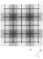
- FIG. 11 is a plan view illustrating a fourth opening and closing pattern of the shutter block in the solid-state imaging device according to the first embodiment of the present technology.
- FIG. 12B is an enlarged plan view of a portion of FIG. 12A.
- 11 is a longitudinal sectional view illustrating a schematic longitudinal sectional structure of a solid-state imaging device according to a second embodiment of the present technology.
- FIG. 11 is a longitudinal sectional view illustrating a modified example 1-1 of the second embodiment of the present technology.
- FIG. 13 is a longitudinal sectional view illustrating a modified example 1-2 of the second embodiment of the present technology.
- FIG. 11 is a longitudinal sectional view illustrating a modified example 1-3 of the second embodiment of the present technology.
- FIG. 13 is a longitudinal sectional view illustrating a modified example 1-4 of the second embodiment of the present technology.
- FIG. 13 is a longitudinal sectional view illustrating a modified example 1-5 of the second embodiment of the present technology.
- FIG. 11 is a plan view illustrating a state in which a portion of each of two shutter sections included in one shutter block overlaps with one photoelectric conversion region in a solid-state imaging device according to a third embodiment of the present technology.
- FIG. 19B is an enlarged plan view of a portion of FIG. 19A.
- 13 is a plan view illustrating a first opening pattern of a shutter block in a solid-state imaging device according to a third embodiment of the present technology.
- FIG. FIG. 20B is an enlarged plan view of a portion of FIG. 20A.
- FIG. 13 is a plan view illustrating a second opening pattern of a shutter block in a solid-state imaging device according to a third embodiment of the present technology.
- FIG. FIG. 20B is an enlarged plan view of a portion of FIG. 20A.
- FIG. 13 is a plan view illustrating a first opening pattern of a shutter block in a modified example 3-1 of the third embodiment of the present technology.
- FIG. 13 is a plan view illustrating a second opening pattern of the shutter block in the modified example 3-1 of the third embodiment of the present technology.
- FIG. 13 is a plan view illustrating a schematic positional relationship between a shutter portion of a shutter layer and a photoelectric conversion region in a modified example 3-2 of the second embodiment of the present technology.
- FIG. 24B is an enlarged plan view of a portion of FIG. 24A.
- 13 is a longitudinal sectional view illustrating a schematic longitudinal sectional structure of a solid-state imaging device according to a fourth embodiment of the present technology.
- FIG. 13 is a perspective view showing an arrangement state of an upper electrode and a lower electrode included in a shutter layer in a solid-state imaging device according to a fourth embodiment of the present technology;
- FIG. 13 is a plan view illustrating an arrangement state of upper electrodes and lower electrodes included in a shutter layer in a solid-state imaging device according to a fourth embodiment of the present technology.
- FIG. 13 is a longitudinal sectional view illustrating a schematic longitudinal sectional structure of a solid-state imaging device according to a fourth embodiment of the present technology.
- FIG. 13 is a perspective view showing an arrangement state of an upper electrode and a lower electrode included in a shutter layer in a solid-state imaging device according to a fourth embodiment of the present technology
- FIG. 13 is a plan view illustrating an
- FIG. 13 is a plan view illustrating a schematic planar pattern of a relay electrode included in an inter-pixel isolation region in a solid-state imaging device according to a fourth embodiment of the present technology.
- FIG. FIG. 13 is a plan view illustrating a modified example 4-1 of the fourth embodiment of the present technology.
- FIG. 13 is a plan view illustrating a modified example 4-2 of the fourth embodiment of the present technology.
- FIG. 13 is a longitudinal sectional view illustrating a modified example 4-3 of the fourth embodiment of the present technology.
- FIG. 13 is a plan view illustrating a modified example 4-3 of the fourth embodiment of the present technology.
- FIG. 13 is a plan view illustrating a modified example 4-4 of the fourth embodiment of the present technology.
- FIG. 13 is a longitudinal sectional view illustrating a schematic longitudinal sectional structure of a solid-state imaging device according to a fifth embodiment of the present technology.
- FIG. FIG. 13 is a diagram showing a configuration example of an electronic device according to a sixth embodiment of the present technology.
- up and down and other directions in the following explanation are merely for the convenience of explanation and do not limit the technical ideas of this technology. For example, if an object is rotated 90 degrees and observed, up and down are converted into left and right and read, and of course, if it is rotated 180 degrees and observed, up and down are read inverted.
- a first direction and a second direction that are mutually orthogonal in the same plane are defined as the X direction and the Y direction, respectively, and a third direction that is orthogonal to each of the first direction and the second direction is defined as the Z direction.
- the thickness direction of the semiconductor layer 21, which will be described later is described as the Z direction.
- the thickness of the semiconductor layer 21 is the distance between the first surface portion S1 and the second surface portion S2, which are located on opposite sides in the Z direction, and the thickness direction of the semiconductor layer 21 is the direction that represents the thickness of the semiconductor layer 21.
- a planar view refers to the semiconductor layer 21 being viewed from the Z direction (one direction).
- a cross-sectional view refers to the cross section along the Z direction (one direction) being viewed from a direction perpendicular to the Z direction.
- CMOS complementary metal oxide semiconductor
- a liquid crystal layer 58 is used as a material layer that can be electrically switched between transmitting and blocking light, and an example is described in which four pseudo pixels are formed in one photoelectric conversion region 22.
- the solid-state imaging device 1A is mainly composed of a semiconductor chip 2 having a rectangular two-dimensional planar shape when viewed in a plane. That is, the solid-state imaging device 1A is mounted on the semiconductor chip 2, and the semiconductor chip 2 can be regarded as the solid-state imaging device 1A. As shown in Fig. 1, the solid-state imaging device 1A according to the first embodiment of the present technology is mainly composed of a semiconductor chip 2 having a rectangular two-dimensional planar shape when viewed in a plane. That is, the solid-state imaging device 1A is mounted on the semiconductor chip 2, and the semiconductor chip 2 can be regarded as the solid-state imaging device 1A. As shown in Fig.
- this solid-state imaging device 1A (101) takes in image light (incident light 106) from a subject via an optical lens 102, converts the amount of incident light 106 imaged on an imaging surface into an electrical signal on a pixel-by-pixel basis, and outputs the electrical signal as a pixel signal.
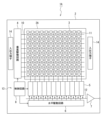
- the semiconductor chip 2 on which the solid-state imaging device 1A is mounted has a square pixel array section 2A located in the center of a two-dimensional plane including mutually orthogonal X and Y directions, and a peripheral section 2B located outside the pixel array section 2A so as to surround the pixel array section 2A.
- the semiconductor chip 2 is formed in the manufacturing process by dicing a semiconductor wafer including a semiconductor layer 21 described below into chip formation regions. Therefore, the configuration of the solid-state imaging device 1A described below is generally the same in the wafer state before the semiconductor wafer is diced. Therefore, this technology can be applied in the semiconductor chip state and in the semiconductor wafer state.
- the column signal processing circuit 5 shown in FIG. 2 is arranged, for example, for each column of pixels 3, and performs signal processing such as noise removal for each pixel column on signals output from one row of pixels 3.
- the column signal processing circuit 5 performs signal processing such as CDS (Correlated Double Sampling) and AD (Analog-to-Digital) conversion to remove pixel-specific fixed pattern noise.
- the horizontal drive circuit 6 shown in FIG. 2 is composed of, for example, a shift register.
- the horizontal drive circuit 6 sequentially outputs horizontal scanning pulses to the column signal processing circuits 5, thereby selecting each of the column signal processing circuits 5 in turn, and causing each of the column signal processing circuits 5 to output a pixel signal that has been subjected to signal processing to the horizontal signal line 12.
- the output circuit 7 shown in FIG. 2 processes and outputs pixel signals sequentially supplied from each of the column signal processing circuits 5 through the horizontal signal line 12.
- the signal processing may include buffering, black level adjustment, column variation correction, various types of digital signal processing, etc.
- the control circuit 8 shown in FIG. 2 generates clock signals and control signals that serve as the basis for the operation of the vertical drive circuit 4, column signal processing circuit 5, horizontal drive circuit 6, etc., based on the vertical synchronization signal, horizontal synchronization signal, and master clock signal. The control circuit 8 then outputs the generated clock signals and control signals to the vertical drive circuit 4, column signal processing circuit 5, horizontal drive circuit 6, etc.
- Each of the plurality of pixels 3 includes a photoelectric conversion region 22 shown in FIG.
- the photoelectric conversion region 22 includes a photoelectric conversion unit 25, a transfer transistor TR, and a floating diffusion region FD as the photoelectric conversion unit.
- Photoelectric conversion section 3 is composed of, for example, a pn junction type photodiode (PD) and generates a signal charge according to the amount of light received.
- the photoelectric conversion unit 25 also temporarily holds (accumulates) the generated signal charge.
- the cathode side of the photoelectric conversion unit 25 is electrically connected to the source region of the transfer transistor TR, and the anode side is electrically connected to a reference potential line (for example, ground).
- Transfer transistor 3 transfers the signal charge photoelectrically converted by the photoelectric conversion unit 25 to the floating diffusion region FD.
- the source region of the transfer transistor TR is electrically connected to the cathode side of the photoelectric conversion unit 25, and the drain region is electrically connected to the floating diffusion region FD.
- the gate electrode of the transfer transistor TR is electrically connected to a transfer transistor drive line of the pixel drive line 10 shown in FIG.
- the floating diffusion region FD shown in FIG. 3 temporarily accumulates and holds the signal charge transferred from the photoelectric conversion unit 25 via the transfer transistor TR.
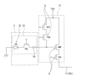
- the solid-state imaging device 1A of the first embodiment further includes a pixel circuit (readout circuit) 15 shown in Fig. 3.
- the input stage of the pixel circuit 15 is electrically connected to the floating diffusion region FD of the photoelectric conversion region 22.
- a circuit configuration is used in which one pixel circuit 15 is assigned to one pixel 3, but this is not limited to this, and one pixel circuit 15 may be shared by multiple pixels 3.
- a circuit configuration may be used in which one pixel circuit 15 is shared by one pixel block, with four pixels 3 arranged in a 2 x 2 arrangement, two by two in each of the X and Y directions, as one unit.
- a circuit configuration may be used in which one pixel circuit 15 is assigned to one pixel block, with two or more pixels 3 as one unit, or a circuit configuration may be used in which one pixel circuit 15 is assigned to multiple pixel blocks, with multiple pixels 3 as one unit.
- the pixel circuit 15 shown in FIG. 3 reads out the signal charge held in the floating diffusion region FD of one pixel 3 and outputs a pixel signal based on the read signal charge.
- the pixel circuit 15 converts the signal charge photoelectrically converted by the photoelectric conversion unit 25 (photodiode PD) into a pixel signal based on this signal charge and outputs it.
- the pixel circuit 15 includes a plurality of pixel transistors Q.
- the pixel circuit 15 of the first embodiment includes, but is not limited to, an amplification transistor AMP, a selection transistor SEL, a reset transistor RST, and a switching transistor FDG as the pixel transistors Q.
- These pixel transistors Q (AMP, SEL, RST, FDG) and the transfer transistor TR described above are configured as insulated gate type field effect transistors, for example, MOSFETs (Metal Oxide Semiconductor Field Effect Transistors) whose gate insulating film is made of a silicon oxide (SiO 2 ) film.
- MOSFETs Metal Oxide Semiconductor Field Effect Transistors
- These transistors may also be MISFETs (Metal Insulator Semiconductor FETs) whose gate insulating film is made of a silicon nitride (Si 3 N 4 ) film or a laminated film of a silicon nitride film and a silicon oxide film.
- MISFETs Metal Insulator Semiconductor FETs
- the selection transistor SEL the reset transistor RST, and the switching transistor FDG function mainly as switching elements.
- the source region of the amplifier transistor AMP is electrically connected to the drain region of the select transistor SEL, the drain region of the amplifier transistor AMP is electrically connected to the power supply line Vdd and the drain region of the reset transistor RST, and the gate electrode of the amplifier transistor AMP is electrically connected to the floating diffusion region FD and the source region of the switching transistor FDG.
- the source region of the selection transistor SEL is electrically connected to the vertical signal line 11 (VSL), the drain region of the selection transistor SEL is electrically connected to the source region of the amplification transistor AMP, and the gate electrode of the selection transistor SEL is electrically connected to the selection transistor driving line of the pixel driving line 10 shown in FIG.
- the amplification transistor AMP constitutes a source follower type amplifier, and outputs a pixel signal having a voltage corresponding to the level of the signal charge generated in the photoelectric conversion unit 25 (photodiode PD).
- the selection transistor SEL is turned on, the amplification transistor AMP amplifies the potential of the floating diffusion region FD and outputs a voltage corresponding to the potential to the column signal processing circuit 5 via the vertical signal line 11 (VSL).
- the FD capacitance C of the floating diffusion region FD needs to be large so that the voltage V when converted to a voltage by the amplifier transistor AMP does not become too large (in other words, to become small).
- the switching transistor FDG when the switching transistor FDG is turned on, the gate capacitance of the switching transistor FDG increases, so the overall FD capacitance C becomes large.
- the switching transistor FDG when the switching transistor FDG is turned off, the overall FD capacitance C becomes small. In this way, by switching the switching transistor FDG on and off, the FD capacitance C can be made variable and the conversion efficiency can be changed.
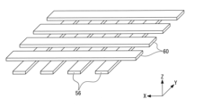
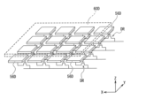
- FIG. 7 is a perspective view showing a schematic arrangement of the upper electrode 60 and the lower electrode 56 included in the shutter layer 51.
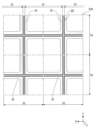
- FIG. 8 is a plan view that shows a schematic arrangement of the upper electrode 60 and the lower electrode 56 included in the shutter layer 51. As shown in FIG.
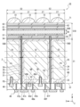
- the semiconductor chip 2 (solid-state imaging device 1A) includes a semiconductor layer 21 having a first surface portion S1 and a second surface portion S2 located on opposite sides in the thickness direction (Z direction) as one direction, a shutter layer 51 provided on the second surface portion S2 side of the semiconductor layer 21, and a lens layer 71 provided on the side of the shutter layer 51 opposite the semiconductor layer 21 side.
- the first surface S1 of the semiconductor layer 21 is sometimes called the main surface or element formation surface, and the second surface S2 is sometimes called the back surface.
- the solid-state imaging device 1A photoelectrically converts incident light incident from the second surface S2 side of the semiconductor layer 21 by a photoelectric conversion section 25 (photodiode PD) provided in the photoelectric conversion region 22 of the semiconductor layer 21. Therefore, in this first embodiment, the second surface S2 of the semiconductor layer 21 is sometimes called the light incident surface.
- the semiconductor layer 21 includes an inter-pixel isolation region 31 extending in the thickness direction (Z direction) of the semiconductor layer 21, and a photoelectric conversion region 22 partitioned by the inter-pixel isolation region 31.
- the photoelectric conversion region 22 is provided for each pixel 3.
- the semiconductor layer 21 may be a Si substrate, a SiGe substrate, an InGaAs substrate, or the like.
- a p-type semiconductor substrate made of single crystal silicon, for example, is used as the semiconductor layer 21.
- the inter-pixel isolation regions 31 extend in the X direction and are repeatedly arranged at predetermined intervals in the Y direction. Also, the inter-pixel isolation regions 31 extend in the Y direction and are repeatedly arranged at predetermined intervals in the X direction. That is, the inter-pixel isolation regions 31 have a lattice-like planar pattern in plan view.
- the pixel separation region 31 corresponding to one photoelectric conversion region 22 has a rectangular annular planar pattern (ring-shaped planar pattern) in a plan view, and surrounds the periphery of one photoelectric conversion region 22.
- the inter-pixel isolation region 31 extends in the thickness direction (Z direction) in which the first surface portion S1 and the second surface portion S2 of the semiconductor layer 21 are separated from each other, and electrically and optically isolates two adjacent photoelectric conversion regions 22 in a plan view of the semiconductor layer 21 from the thickness direction (Z direction) of the semiconductor layer 21.
- the inter-pixel isolation region 31 is, for example but not limited to, configured as a trench isolation type including a recessed portion 32 extending in the thickness direction (Z direction) of the semiconductor layer 21 and an isolation insulating film 34 provided in the recessed portion 32.
- the inter-pixel isolation region 31 reaches both the first surface portion S1 and the second surface portion S2 of the semiconductor layer 21.
- the photoelectric conversion region 22 is surrounded by inter-pixel isolation regions 31 in a plan view and has a rectangular planar shape.
- the photoelectric conversion region 22 is partitioned by the inter-pixel isolation regions 31 and is separated from other photoelectric conversion regions 22.
- the photoelectric conversion regions 22 are repeatedly arranged in the mutually orthogonal X and Y directions in a two-dimensional plane, with inter-pixel isolation regions 31 between them, and are provided for each pixel 3. That is, the photoelectric conversion regions 22 are arranged in a matrix (row and column) in the pixel array section 2A shown in FIG. 1, similar to the pixels 3.
- the photoelectric conversion region 22 has a p-type well region 23 consisting of a p-type semiconductor region provided in the semiconductor layer 21 across the first surface portion S1 and the second surface portion S2 of the semiconductor layer 21, an n-type semiconductor region 24 provided in the p-type well region 23 away from the first surface portion S1 of the semiconductor layer 21, and a photoelectric conversion section 25 including the p-type well region 23 and the n-type semiconductor region 24 and provided in the semiconductor layer 21 away from the first surface portion S1 of the semiconductor layer 21.
- the photoelectric conversion region 22 further includes an n-type floating diffusion region FD that is provided on the first surface portion S1 of the semiconductor layer 21 and overlaps with the n-type semiconductor region 24 in a planar view, and serves as a charge storage portion that stores signal charges photoelectrically converted by the photoelectric conversion portion 25, and a transfer transistor TR that is provided on the first surface portion S1 of the semiconductor layer 21 and overlaps with the n-type semiconductor region 24 in a planar view, and transfers the signal charges photoelectrically converted by the photoelectric conversion portion 25 to the n-type floating diffusion region FD.
- the photoelectric conversion region 22 further includes, for example, an amplification transistor AMP, a selection transistor SEL, a reset transistor RST, and a switching transistor FDG as pixel transistors Q included in the pixel circuit 15 of FIG. 3, although these are not shown.
- These pixel transistors Q (AMP, SEL, RST, FDG) are provided on the first surface portion S1 side of the semiconductor layer 21 in the photoelectric conversion region 22.
- the p-type well region 23 is provided over a wide area across the first surface portion S1 side and the second surface portion S2 side of the semiconductor layer 21 in each photoelectric conversion region 22.
- the p-type well region 23 contacts the inter-pixel isolation region 31 along the thickness direction (Z direction) of the semiconductor layer 21.
- the n-type semiconductor region 24 is provided in the p-type well region 23 in each photoelectric conversion region 22. That is, the n-type semiconductor region 24 is surrounded by the p-type well region 23 on six sides, including the top surface, bottom surface, and four side surfaces. The n-type semiconductor region 24 is separated from the first surface portion S1 and the second surface portion S2 of the semiconductor layer 21, and the inter-pixel isolation region 31.
- Photoelectric conversion section 5 includes a p-type well region 23 and an n-type semiconductor region 24 in each photoelectric conversion region 22.
- the photoelectric conversion unit 25 is configured as a pn junction type photodiode (PD) including a pn junction between the p-type well region 23 and the n-type semiconductor region 24.
- PD pn junction type photodiode
- the photoelectric conversion section 25 photoelectrically converts light incident on the n-type semiconductor region 24 from the second surface S2 side of the semiconductor layer 21 into a signal charge in the n-type semiconductor region 24, and temporarily holds (accumulates) the photoelectrically converted signal charge at the pn junction between the p-type well region 23 and the n-type semiconductor region 24. That is, the semiconductor layer 21 has the second surface S2 as a light incident surface, and photoelectric conversion regions 22 that photoelectrically convert light incident from the second surface S2 into a signal charge in the photoelectric conversion section 25 are arranged in a matrix.
- the n-type floating diffusion region FD is provided in the p-type well region 23 on the first surface portion S1 side of the semiconductor layer 21.
- the n-type floating diffusion region FD overlaps with the n-type semiconductor region 24 of the photoelectric conversion unit 25 in a plan view, and is separated from the n-type semiconductor region 24 of the photoelectric conversion unit 25 in the thickness direction (Z direction) of the semiconductor layer 21. That is, the p-type well region 23 is provided between the n-type floating diffusion region FD and the n-type semiconductor region 24.
- the n-type floating diffusion region FD is composed of an n-type semiconductor region having a higher impurity concentration than the n-type semiconductor region 24.
- the n-type floating diffusion region FD is covered with an interlayer insulating film 46 provided on the first surface portion S1 side of the semiconductor layer 21.
- the n-type floating diffusion region FD is electrically connected to a wiring 48f provided in the wiring layer 48 via a contact electrode 47f provided in the interlayer insulating film 46.
- the transfer transistor TR is provided on the first surface S1 side of the semiconductor layer 21 (the first surface S1 side of the photoelectric conversion region 22).
- the transfer transistor TR has a gate electrode 43 provided across the inside and outside of the semiconductor layer 21 on the first surface S1 side of the photoelectric conversion region 22 (semiconductor layer 21), and a gate insulating film 42 provided between the gate electrode 43 and the semiconductor layer 21.
- the transfer transistor TR further includes an n-type semiconductor region 24 that functions as a source region, an n-type floating diffusion region FD that functions as a drain region, and a p-type well region 23 that functions as a channel formation region.
- This transfer transistor RT is configured as a vertical type.
- the gate electrode 43 of the transfer transistor TR is covered with an interlayer insulating film 46 provided on the first surface portion S1 side of the semiconductor layer 21.
- the gate electrode 43 is electrically connected to a wiring 48t provided in the wiring layer 48 via a contact electrode 47t provided in the interlayer insulating film 46.
- the shutter layer 51 has, sequentially from the second surface S2 side of the semiconductor layer 21, a polarizing plate 54, an insulating film 55, a lower electrode 56, an alignment film 57, a liquid crystal layer 58, an alignment film 59, an upper electrode 60, an insulating film 61, a polarizing plate 62, and an insulating film 63.
- the liquid crystal layer 58 is used as a material layer that can be electrically switched between transmitting and blocking light. 4 to 6B as a shutter portion that is provided on the light incident surface portion side (second surface portion S2) of the semiconductor layer 21 and controls the incidence of light to the photoelectric conversion region 22 by transmitting (open state) and blocking (closed state).
- the shutter layer 51 also has a shutter block 53 shown in FIG. 6A.
- the upper electrodes 60 extend in the X direction and are repeatedly arranged at a predetermined interval in the Y direction with an arrangement pitch identical to the arrangement pitch 52Py of the shutter sections 52 in the Y direction.
- the lower electrodes 56 extend in the Y direction and are repeatedly arranged at a predetermined interval in the Y direction with an arrangement pitch identical to the arrangement pitch 52Px of the shutter sections 52 in the X direction.
- An intersection where the upper electrode 60 and the lower electrode 56 intersect is provided at a position overlapping the shutter section 52 in a plan view.
- Each of the upper electrode 60 and the lower electrode 56 is made of a transparent conductive film such as ITO (Indium Tin Oxide).
- the shutter sections 52 are repeatedly arranged in a tiled manner in each of the X direction and the Y direction which are perpendicular to each other in a two-dimensional plane.
- the shutter sections 52 are repeatedly arranged in the X direction with an arrangement pitch 52Px, and are repeatedly arranged in the Y direction with an arrangement pitch 52Py.
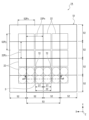
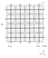
- the shutter block 53 includes a plurality of shutter sections 52 each of which partially overlaps with one photoelectric conversion region 22 in a plan view as one unit.
- the plurality of shutter sections 52 included in the shutter block 53 are, for example, four shutter sections 52 (52a, 52b, 52c, 52d) arranged adjacent to each other in each of the X direction and the Y direction perpendicular to each other in the same plane, but are not limited thereto.
- the shutter blocks 53 are repeatedly arranged in each of the X direction and the Y direction to construct a shutter block array in the shutter layer 51. That is, the shutter layer 51 has a shutter block array in which a plurality of shutter blocks 53 each including four shutter sections 52 arranged in a 2 x 2 arrangement as one unit are arranged in a matrix.
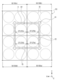
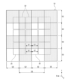
- each of the four shutter sections 52 included as one unit in one shutter block 53 is shifted in position relative to the photoelectric conversion region 22 in the X direction by an amount equivalent to half the arrangement pitch 22Px of the photoelectric conversion region 22 in the X direction. Also, each of the four shutter sections 52 included as one unit in one shutter block 53 is shifted in position relative to the photoelectric conversion region 22 in the Y direction by an amount equivalent to half the arrangement pitch 22Py of the photoelectric conversion region 22 in the Y direction. That is, each of the four shutter sections 52 included in the shutter block 53 overlaps evenly with one photoelectric conversion region 22 in a planar view.
- one photoelectric conversion region 22 includes four overlapping regions 27 (27a, 27b, 27c, 27d) in which a portion of each of the four shutter sections 52 overlaps individually, as shown in FIG. 4 and FIG. 6A.
- Each of the four overlapping regions 27 (27a, 27b, 27c, 27d) functions as a pseudo pixel, and one photoelectric conversion region 22 constitutes four pseudo pixels.
- each of the four adjacent shutter sections 52 (52a, 52b, 52c, 52d) in a plan view has a portion overlapping with one photoelectric conversion region 22.
- each of the four adjacent photoelectric conversion regions 22 has a portion overlapping with one shutter section 52.
- the lens layer 71 is provided with microlenses 72 that collect light (irradiated light) and allow the collected light to efficiently enter the photoelectric conversion region 22.
- the microlenses 72 are provided for each of four overlapping regions 27 (27a, 27b, 27c, 27d) in one photoelectric conversion region 22 where a portion of each of the four shutter sections 52 overlaps with each other. That is, one pixel 3 includes four microlenses 72 that individually overlap with each of the four overlapping regions 27 of the photoelectric conversion region 22 in a plan view.
- FIG. 9A is a plan view illustrating a schematic diagram of a first opening pattern of a shutter block.
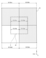
- FIG. 9B is an enlarged plan view of a portion of FIG. 9A.
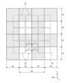
- FIG. 10A is a plan view illustrating a schematic view of a second opening pattern of the shutter block.
- FIG. 10B is an enlarged plan view of a portion of FIG. 10A.
- FIG. 11A is a plan view illustrating a schematic view of a third opening pattern of the shutter block.
- FIG. 11B is an enlarged plan view of a portion of FIG. 11A.
- FIG. 12A is a plan view illustrating a schematic view of a fourth opening pattern of the shutter block.
- FIG. 12B is an enlarged plan view of a portion of FIG. 12A.
- the shutter portion 52 in the closed state is given a dot pattern
- the shutter portion 52 in the open state is given no dot pattern.
- the shutter block 53 of this first embodiment includes, as a unit, four shutter sections 52 (52a, 52b, 52c, 52d), each of which partially overlaps with one photoelectric conversion region 22 in a plan view.
- the first opening pattern in which the shutter section 52a of the four shutter sections 52 (52a, 52b, 52c, 52d) is opened and the remaining three shutter sections 52b, 52c, 52d are closed allows light to be selectively incident on the overlapping region 27a (first pseudo pixel) of the photoelectric conversion region 22.
- a third opening pattern in which, of the four shutter sections 52 (52a, 52b, 52c, 52d), shutter section 52c is opened and the remaining three shutter sections 52a, 52b, 52d are closed allows light to selectively enter the overlapping region 7c (third pseudo pixel) of the photoelectric conversion region 22.
- a fourth opening pattern in which, of the four shutter sections 52 (52a, 52b, 52c, 52d), shutter section 52d is in an open state and the remaining three shutter sections 52a, 52b, 52c are in a closed state allows light to selectively enter the overlapping region 27d (fourth pseudo pixel) of the photoelectric conversion region 22.
- this single shutter block 53 can partially open one photoelectric conversion region 22 in four separate steps using the four shutter sections 52 (52a, 52b, 52c, 52d), allowing light to enter one photoelectric conversion region 22 partially in four separate steps.
- a first image is taken with the first aperture pattern shown in Figures 9A and 9B
- a second image is taken with the second aperture pattern shown in Figures 10A and 10B
- a third image is taken with the third aperture pattern shown in Figures 11A and 11B
- a fourth image is taken with the fourth aperture pattern shown in Figures 12A and 12B.
- the solid-state imaging device 1A according to the first embodiment can achieve high resolution.
- the four shutter sections 52 included as one unit in one shutter block 53 are shifted in position relative to the photoelectric conversion area 22 by an amount equivalent to half the arrangement pitch (22Px, 22Py) of the photoelectric conversion area 22 in each of the X and Y directions, so that the accuracy of each image captured four times can be made uniform, and the image quality performance of the composite image can be improved.
- liquid crystal layer 58 which is resistant to the crosstalk phenomenon between adjacent pixels 3.
- FIG. 13 is a longitudinal sectional view that illustrates a schematic longitudinal sectional structure of a solid-state imaging device according to a second embodiment of the present technology.
- the solid-state imaging device 1B according to the second embodiment of the present technology is basically configured similarly to the solid-state imaging device 1A according to the first embodiment described above, with the following differences.
- the solid-state imaging device 1B according to the second embodiment further includes a color filter layer 65 that transmits light of a specific wavelength.
- This technology can also be applied to a solid-state imaging device 1B that includes a color filter layer 65.
- the color filter layer 65 is provided on the side opposite the semiconductor layer 21 of the shutter layer 51.
- the color filter layer 65 is provided between the shutter layer 51 and the lens layer 71.
- the color filter layer 65 includes a plurality of filter portions (color filter portions) 66.
- the color filter layer 65 of the second embodiment includes, but is not limited to, a filter portion 66 that transmits light of a specific wavelength, such as red (R), green (G), or blue (B), for each shutter portion 52.
- the color filter layer 65 also includes a separation wall (filter separation wall) 67 between adjacent filter portions 66 to suppress color mixing. It is preferable to use a low refractive index material having a lower refractive index than the filter portion 66 as the material for the separation wall 67.
- the solid-state imaging device 1B according to the second embodiment also provides the same effects as the solid-state imaging device 1A according to the first embodiment described above.
- FIG. 14 is a vertical cross-sectional view illustrating a modified example 2-1 of the second embodiment of the present technology.
- this modified example 2-1 includes a separation wall (shutter separation wall) 64 between adjacent shutter sections 52 to suppress uneven transmission.
- the separation wall 64 is provided in the liquid crystal layer 58 for each shutter section 52, and is configured in an annular planar pattern corresponding to the planar shape of the shutter section 52.
- the separation wall 64 is provided in the liquid crystal layer 58 in a lattice-like planar pattern corresponding to the matrix arrangement of the shutter sections 52.
- the liquid crystal layer 58 is divided into each shutter section 52 by the separation wall 64. That is, the shutter section 52 is divided into a plurality of sub-regions by the separation wall 64. It is preferable to use an insulating material as the material for the separation wall 64.
- the separation wall 64 can suppress uneven transmission between adjacent shutter sections 52 in a plan view, thereby achieving even higher image quality.
- the separation wall 64 can also be applied to the solid-state imaging device 1A according to the first embodiment described above, which does not include the color filter layer 65 shown in FIG. 14.
- FIG. 15 is a longitudinal sectional view diagrammatically illustrating Modification 2-2 of the second embodiment of the present technology.
- a separation wall 64 is provided even within one shutter section 52 to prevent incident light from entering adjacent pixels.
- the separation walls 64 in this modified example 2-2 are provided in the liquid crystal layer 58 in a planar pattern that individually surrounds, in a planar view, each of the four overlapping regions 27 included in one photoelectric conversion region 22.
- the liquid crystal layer 58 that overlaps with one shutter section 52 in a planar view is divided into each overlapping region 27 by the separation walls 64.
- the separation wall 64 can prevent incident light from penetrating into adjacent pixels (color mixing), thereby further improving the image quality performance of the composite image.
- the configuration in which the separation wall 64 is disposed inside the shutter section 52 can also be applied to the solid-state imaging device 1A according to the first embodiment described above.
- FIG. 16 is a longitudinal sectional view diagrammatically illustrating Modification 2-3 of the second embodiment of the present technology. As shown in FIG. 16, this modification 2-3 is obtained by changing the arrangement of the filter portions 66 of the color filter layer 65 in the above-mentioned modification 2-2.
- the filter portion 66 of the color filter layer 65 overlaps with the shutter portion 52 for each shutter portion 52 in a plan view.
- the filter portion 66 of the color filter layer 65 overlaps the photoelectric conversion region 22 for each photoelectric conversion region 22 in a planar view.
- the filter portion 66 of this modified example 2-3 overlaps with a portion of each of the four shutter portions 52 included in one shutter block 53 in a planar view.
- FIG. 17 is a longitudinal sectional view diagrammatically illustrating a modified example 2-4 of the second embodiment of the present technology.
- filter portions 66 of the color filter layer 65 are arranged so as to overlap with the overlapping regions 27 of the photoelectric conversion regions 22 in a plan view. Separation walls 67 are provided between the filter portions 66 adjacent to each other.
- This modification 2-4 also provides the same effects as the solid-state imaging device 1B according to the second embodiment described above.
- FIG. 18 is a longitudinal sectional view diagrammatically illustrating a modified example 2-5 of the second embodiment of the present technology.
- this modification 2-5 is the same as the above modification 2-4 in that the position of the color filter layer 65 is changed.
- a color filter layer 65 is provided between the shutter layer 51 and the lens layer 71 on the side of the shutter layer 51 opposite the semiconductor layer 21 side.
- the color filter layer 65 is provided on the semiconductor layer 21 side of the shutter layer 51. And, in this modified example 2-3, the color filter layer 65 is provided between the shutter layer 51 and the semiconductor layer 21.
- the arrangement of the color filter layer 65 in this modified example 2-5 can also be applied to the second embodiment described above, and can also be applied to any of the modified examples 2-1 to 2-3 described above.
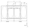
- FIG. 19A is a plan view diagrammatically showing a state in which a portion of each of two shutter sections 52 included in one shutter block 53C overlaps with one photoelectric conversion region 22 in a solid-state imaging device 1C relating to the third embodiment of the present technology.
- FIG. 19B is an enlarged plan view of a portion of FIG. 19A.
- the solid-state imaging device 1C according to the third embodiment of the present technology is basically configured similarly to the solid-state imaging device 1A according to the first embodiment described above, with the following differences.
- a solid-state imaging device 1C according to the third embodiment of the present technology includes a shutter block 53C instead of the shutter block 53 shown in Figures 4 and 6A of the first embodiment described above. Also, the shape and arrangement of the microlenses 72 included in the lens layer 71 are different. The other configurations are generally similar to those of the first embodiment described above.
- the shutter block 53C includes a plurality of shutter sections 52 each of which overlaps with one photoelectric conversion region 22 in a plan view as one unit.
- the plurality of shutter sections 52 included in the shutter block 53C are, but are not limited to, for example, two shutter sections 52 (52a, 52b) arranged adjacent to each other in the X direction, out of the X direction and the Y direction which are orthogonal to each other in the same plane.
- the shutter blocks 53C are arranged repeatedly in each of the X direction and the Y direction, forming a shutter block array in the shutter layer 51. That is, the shutter layer 51 of this third embodiment has a shutter block array in which a plurality of shutter blocks 53C each including two shutter sections 52 arranged in a 1 x 2 arrangement in the X direction as one unit are arranged in a matrix.
- each of the two shutter sections 52 included as one unit in one shutter block 53C is shifted in position in the X direction relative to the photoelectric conversion region 22 by an amount equivalent to half the arrangement pitch 22Px of the photoelectric conversion region 22 in the X direction. That is, each of the two shutter sections 52 included in the shutter block 53C overlaps evenly with one photoelectric conversion region 22 in a planar view.
- One photoelectric conversion region 22 includes two overlapping regions 27 (27a, 27b) in which portions of the two shutter sections 52 overlap individually. Each of the two overlapping regions 27 (27a, 27b) functions as a pseudo pixel, and one photoelectric conversion region 22 constitutes two pseudo pixels.
- two shutter sections 52 (52a, 52b) adjacent to each other in a planar view have a portion overlapping with one photoelectric conversion region 22.
- two photoelectric conversion regions 22 adjacent to each other in the X direction have a portion overlapping with one shutter section 52.
- the microlenses 72 of this third embodiment are provided for each of two overlapping regions 27 (27a, 27b) in which portions of two shutter sections 52 individually overlap in one photoelectric conversion region 22. That is, one pixel 3 of this third embodiment includes two microlenses 72 that individually overlap each of the two overlapping regions 27 of the photoelectric conversion region 22 in a plan view.
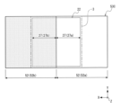
- FIG. 20A is a plan view illustrating a schematic first opening pattern of the shutter block.
- FIG. 20B is an enlarged plan view of a portion of FIG. 20A.
- FIG. 21A is a plan view illustrating a schematic view of a second opening pattern of the shutter block.
- FIG. 21B is an enlarged plan view of a portion of FIG. 21A.
- the shutter portion 52 in the closed state is given a dot pattern, and the shutter portion 52 in the open state is given no dot pattern.
- the shutter block 53C of this third embodiment includes two shutter sections 52 (52a, 52b) each of which partially overlaps with one photoelectric conversion region 22 in a plan view as one unit.
- the first opening pattern opens one of the two shutter sections 52 (52a, 52b), 52a, and closes the other shutter section 52b, allowing light to selectively enter the overlapping region 27a (first pseudo pixel) of the photoelectric conversion region 22.
- a second opening pattern in which the other shutter section 52b of the two shutter sections 52 (52a, 52b) is opened and the remaining shutter section 52a is closed allows light to be selectively incident on the overlapping region 7b (second pseudo pixel) of the photoelectric conversion region 22.
- this single shutter block 53C can partially open one photoelectric conversion region 22 in two separate steps using two shutter sections 52 (52a, 52b), allowing light to enter one photoelectric conversion region 22 partially in two separate steps.
- the opening and closing of the shutter units 52 is performed, for example, for each shutter row in which multiple shutter units 52 are lined up in the Y direction.
- the solid-state imaging device 1C according to the third embodiment can achieve high resolution.
- the two shutter sections 52 included as one unit in one shutter block 53C are shifted in position relative to the photoelectric conversion area 22 in the X direction by an amount equivalent to half the pitch (1/2 pitch) of the arrangement pitch (22Px) of the photoelectric conversion area 22, so that the precision of each image captured twice can be made uniform, and the image quality performance of the composite image can be improved.
- the liquid crystal layer 58 it is preferable to use a ferroelectric liquid crystal for the liquid crystal layer 58, which is resistant to the crosstalk phenomenon between adjacent pixels 3.
- the shutter block 53 of this third embodiment can also be applied to the second embodiment described above, and can also be applied to any of the modified examples 2-1 to 2-5 described above.
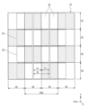
- FIG. 22 is a plan view diagrammatically illustrating a first opening pattern of a shutter block 53C in the modified example 3-1 of the third embodiment of the present technology.
- FIG. 23 is a plan view diagrammatically illustrating a second opening pattern of the shutter block 53C in the modified example 3-1 of the second embodiment of the present technology.
- the shutter portion 52 in the closed state is given a dot pattern, and the shutter portion 52 in the open state is given no dot pattern.
- the open and closed states of the shutter section 52 are in a checkered pattern. That is, in the first opening pattern shown in Figures 20A and 20B, as shown in Figure 22, a first checkered pattern is created in which the open shutter section 52 and the closed shutter section 52 are alternately lined up in the X and Y directions, and in the second opening pattern shown in Figures 21A and 21B, a second checkered pattern is created in which the opening and closing states of the shutter section 52 in the first checkered pattern are reversed (the open shutter section 52 is in the closed state, and the closed shutter section 52 is in the open state).
- a shutter block 53C2 is provided instead of the shutter block 53C of the above-mentioned third embodiment.
- FIG. 24A is a plan view that shows a schematic diagram of the positional relationship between the shutter portion 52 of the shutter layer 51 and the photoelectric conversion region 22 in modified example 3-2 of the second embodiment of the present technology.
- FIG. 24B is an enlarged plan view of a portion of FIG. 24A.
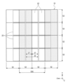
- the shutter block 53C of the third embodiment described above includes two shutter sections 52 (52a, 52b) arranged adjacent to each other in the X direction as a unit, with each shutter section 52 having a portion that overlaps with one photoelectric conversion region 22 in a plan view.
- the shutter blocks 53C are then repeatedly arranged in both the X and Y directions to form a shutter block array in the shutter layer 51.
- the shutter block 53C2 of the modified example 3-2 includes two shutter sections 52 (52a, 52b) arranged adjacent to each other in the Y direction as one unit, with each shutter section 52 being a plurality of shutter sections 52, a portion of which overlaps with one photoelectric conversion region 22 in a plan view.
- the shutter blocks 53C2 are repeatedly arranged in both the X direction and the Y direction to form a shutter block array in the shutter layer 51. That is, the shutter layer 51 of the modified example 3-2 has a shutter block array in which a plurality of shutter blocks 53C2, each including two shutter sections 52 arranged in a 1 ⁇ 2 arrangement arranged in the Y direction as one unit, are arranged in a matrix.
- each of the two shutter sections 52 included as one unit in one shutter block 53C2 is shifted in position in the Y direction relative to the photoelectric conversion region 22 by an amount equivalent to half the arrangement pitch 22Py of the photoelectric conversion region 22 in the Y direction. That is, each of the two shutter sections 52 included in the shutter block 53C2 overlaps evenly with one photoelectric conversion region 22 in a plan view.
- One photoelectric conversion region 22 includes two overlapping regions 27 (27a, 27b) in which parts of the two shutter sections 52 overlap with each other.
- Each of the two overlapping regions 27 (27a, 27b) functions as a pseudo pixel, and one photoelectric conversion region 22 constitutes two pseudo pixels.
- two adjacent shutter sections 52 (52a, 52b) in a plan view each have a portion overlapping with one photoelectric conversion region 22.
- two adjacent photoelectric conversion regions 22 in the X direction each have a portion overlapping with one shutter section 52.
- the microlenses 72 of this modified example 3-2 are provided for each of two overlapping regions 27 (27a, 27b) in which portions of two shutter sections 52 individually overlap in one photoelectric conversion region 22. That is, one pixel 3 of this modified example 3-2 includes two microlenses 72 that individually overlap each of the two overlapping regions 27 of the photoelectric conversion region 22 in a planar view, similar to the third embodiment described above.
- a shutter block 53C2 of this modification 3-2 includes, as one unit, two shutter portions 52 (52a, 52b) each of which partially overlaps with one photoelectric conversion region 22 in a plan view.
- a first opening pattern in which one of the two shutter sections 52 (52a, 52b), 52a, is in an open state and the other shutter section 52b is in a closed state enables selective incidence of light into the overlap region 27a (first pseudo pixel) of the photoelectric conversion region 22.
- two shutter sections 52 can partially open one photoelectric conversion region 22 in two separate steps, and light can be incident partially on one photoelectric conversion region 22 in two separate steps.
- a first image is taken with the first aperture pattern and a second image is taken with the second aperture pattern; that is, by obtaining two images by changing the aperture position, an image with twice the resolution, as if it were taken with pixels with half the pitch of the actual pixel 3, can be synthesized.
- the opening and closing of the shutter sections 52 is performed, for example, for each shutter row in which a plurality of shutter sections 52 are lined up in the Y direction.
- this modified example 3-2 as well, it is possible to achieve high resolution in the same way as in the above-described third embodiment.
- the two shutter sections 52 included as one unit in one shutter block 53C2 are shifted in position relative to the photoelectric conversion region 22 in the Y direction by an amount equivalent to half the pitch (1/2 pitch) of the arrangement pitch (22Py) of the photoelectric conversion region 22, so that, as in the third embodiment described above, the accuracy of each image taken twice can be made uniform, and the image quality performance of the composite image can be improved.
- the shutter units 52 can be opened or closed for each shutter row in which multiple shutter units 52 are lined up in the Y direction, as in the third embodiment described above. Also, the shutter units 52 can be opened or closed in a checkerboard pattern, as in modified example 3-1 described above.
- FIG. 25 is a longitudinal sectional view that illustrates a schematic longitudinal sectional structure of a solid-state imaging device according to a fourth embodiment of the present technology.
- FIG. 26 is a perspective view illustrating an arrangement state of upper electrodes and lower electrodes included in a shutter layer in a solid-state imaging device according to a fourth embodiment of the present technology.
- FIG. 27 is a plan view illustrating an arrangement state of upper electrodes and lower electrodes included in a shutter layer in a solid-state imaging device according to a fourth embodiment of the present technology.
- FIG. 28 is a plan view that illustrates a planar pattern of relay electrodes included in an inter-pixel isolation region in a solid-state imaging device according to a fourth embodiment of the present technology.
- the solid-state imaging device 1D according to the fourth embodiment of the present technology is basically configured similarly to the solid-state imaging device 1A according to the first embodiment described above, with the following differences.
- a solid-state imaging device 1D according to the fourth embodiment of the present technology has an active matrix type shutter layer 51D instead of the simple matrix type shutter layer 51 shown in FIG. 5 of the first embodiment described above. Also, the configuration of the inter-pixel isolation region 31 is different. The other configurations are generally similar to those of the first embodiment described above.
- the shutter layer 51D has a structure basically similar to that of the liquid crystal layer 51 of the above-mentioned first embodiment shown in Fig. 5, and includes an upper electrode 60D and a lower electrode 56D instead of the upper electrode 60 and the lower electrode 56 shown in Fig. 5. That is, the shutter layer 51D has a polarizing plate 54, an insulating film 55, a lower electrode 56D, an alignment film 57, a liquid crystal layer 58, an alignment film 59, an upper electrode 60D, an insulating film 61, a polarizing plate 62, and an insulating film 63, which are provided in this order from the second surface S2 side of the semiconductor layer 21.
- the upper electrode 60D spreads over a wide area across multiple shutter sections 52 and is shared by multiple shutter sections.
- the lower electrode 56D is provided for each shutter section 52.
- Each of the upper electrode 60D and the lower electrode 56D is made of a transparent conductive film such as ITO (Indium Tin Oxide).
- the shutter section 52 of the fourth embodiment includes an upper electrode 60D and a lower electrode 56D.
- the shutter section 52 applies a voltage to the upper electrode 60D and the lower electrode 56D, generating an electric field between the upper electrode 60D and the lower electrode 56D to drive the liquid crystal molecules of the liquid crystal layer 56 to an open state (transmitting state) or a closed state (blocking state), thereby controlling the incidence of light into the photoelectric conversion region 22.
- a voltage is applied to the lower electrode 56D by a drive transistor DR provided for each lower electrode 56. That is, the shutter layer 51D is configured, for example, in an active matrix manner, although this is not limited to this. In the active matrix manner, the shutter section 52 to be selected is selected by a drive transistor DR electrically connected to the lower electrode 56.
- the configuration of the shutter section and shutter block in this fourth embodiment is generally similar to the shutter section 52 and shutter block 53 in the first embodiment described above, except for the upper electrode 60D and lower electrode 56D.
- the driving transistor DR is provided on the first surface S1 side of the semiconductor layer 21 in the photoelectric conversion region 22.
- the driving transistor DR has a gate electrode 43d provided on the outside of the first surface S1 of the semiconductor layer 21, and a gate insulating film 42 provided between the gate electrode 43d and the first surface S1 of the semiconductor layer 21.
- the driving transistor DR further has a pair of main electrode regions 49a and 49b provided in the surface layer portion on the first surface S1 side of the semiconductor layer 21 and functioning as a source region and a drain region, and a p-type well region 23 functioning as a channel formation portion.
- Each of the pair of main electrode regions 49a and 49b is composed of an n-type semiconductor region having a higher impurity concentration than the n-type semiconductor region 24.
- one main electrode region 49a of the drive transistor DR is electrically connected to a wiring 48m provided in the wiring layer 48 via a contact electrode 47m provided in the interlayer insulating film 46.
- the other main electrode region 49b of the drive transistor DR is electrically connected to a wiring 48n provided in the wiring layer 48 via a contact electrode 47n provided in the interlayer insulating film 46.
- the inter-pixel isolation region 31 of the fourth embodiment includes a relay electrode 35. That is, the inter-pixel isolation region 31 of the fourth embodiment includes a dug portion 32 extending in the thickness direction (Z direction) of the semiconductor layer 21, an isolation insulating film 34 provided along the sidewall of the dug portion 32, and a relay electrode 35 provided in the dug portion 32 with the isolation insulating film 34 interposed therebetween.
- one end of the relay electrode 35 protrudes from the second surface S2 of the semiconductor layer 21 to the shutter layer 51D and is electrically and mechanically connected to the lower electrode 56D.
- the other end of the relay electrode 35 is electrically and mechanically connected to a contact electrode 47p provided in the interlayer insulating film 46.
- the contact electrode 47p is electrically and mechanically connected to a wiring 48n provided in the wiring layer 48. That is, the lower electrode 56D is electrically connected to the main electrode region 49b of the drive transistor DR via the relay electrode 35, the contact electrode 47p, the wiring 48n, and the contact electrode 47n.
- the relay electrodes 35 are provided for each shutter section 52, and are electrically and structurally isolated from the other adjacent relay electrodes 35. Although not limited to this, the relay electrodes 35 are configured in a cross shape in a plan view, and are provided between four adjacent photoelectric conversion regions in each of the X and Y directions.
- the relay electrodes 35 may be configured with individually separated dot patterns. In this case, multiple relay electrodes 35 are electrically connected to each liquid crystal shutter layer 52.
- the present technology can be applied to the active matrix shutter layer 51D, and the solid-state imaging device 1D according to the fourth embodiment can achieve the same effects as the first embodiment described above.
- the color filter layer 65 of the second embodiment and modification 2-5 can be applied to the solid-state imaging device 1D of the fourth embodiment.
- the techniques relating to the separation walls 64 and 67 in the above-described modified examples 2-1 to 2-4 can be applied to the solid-state imaging device 1D of the fourth embodiment.
- the polarizing plates 54 and 62 may be a combination of polarizing plates having linear polarizers of "0°”, “45°”, “90°”, and "135°".
- the overlapping manner of the polarizing plates 54 and 62 with the shutter section 52 (lower electrode 56D) and the photoelectric conversion region 22 (pixel 3) allows the same usage in the case of transmission every 1/4 size, but can be used as a different sensor when used in the case of transmission of all pixels.
- FIG. 29 is a plan view diagrammatically illustrating a modified example 4-1 of the fourth embodiment of the present technology.
- FIG. 30 is a plan view diagrammatically illustrating a modified example 4-2 of the fourth embodiment of the present technology. 29 shows a modified example 4-1 in which the polarizing plates 54 and 62 and the shutter section 52 (lower electrode 56D) overlap at the same position.
- this modified example 4-1 all pixels are transparent, and four polarized lights are mixed, so that it can be used like a normal sensor.
- Modification 4-2 shown in FIG. 30 is a case where the polarizing plates 54, 62 and the photoelectric conversion region 22 (pixel 3) overlap at the same position.
- this modification 4-2 all pixels are transparent, and each pixel can be used as a polarization sensor with a linear polarizer in one direction.
- FIG. 31 is a longitudinal sectional view diagrammatically illustrating Modification 4-3 of the fourth embodiment of the present technology.
- FIG. 32 is a plan view diagrammatically illustrating a modified example 4-3 of the fourth embodiment of the present technology.
- FIG. 33 is a plan view diagrammatically illustrating Modification 4-4 of the fourth embodiment of the present technology.
- Fig. 31 in a solid-state imaging device in which the color filter layer 65 and the liquid crystal layer 58 shown in Fig. 16 of the above-mentioned modified example 2-3 are applied to the fourth embodiment, modified example 4-3 in Fig.
- modified example 4-4 in FIG. 33 is a case in which the polarizing plates 54, 62 and the photoelectric conversion region 22 (pixel 3) overlap at the same position, and the filter section 66 and the shutter section 52 (lower electrode 56D) overlap at the same position.
- all pixels are transparent, and it can be used as a polarization sensor that mixes R+G+B light.
- FIG. 34 is a longitudinal sectional view that typically illustrates a longitudinal sectional structure of a solid-state imaging device 1E according to a fifth embodiment of the present technology.
- the solid-state imaging device 1E according to the fifth embodiment of the present technology is basically configured similarly to the solid-state imaging device 1A according to the first embodiment described above, with the following differences.
- the solid-state imaging device 1E according to the fifth embodiment of the present technology has an electrochromic material layer 58E instead of the liquid crystal layer 58 shown in FIG. 5 of the first embodiment described above.
- the solid-state imaging device 1E according to the fifth embodiment of the present technology omits the polarizing plates 54 and 62, the alignment films 57 and 59, and the insulating film 63 shown in FIG. 5.
- the other configurations and driving methods are generally similar to those of the first embodiment described above.
- the shutter section 52 controls the transmission and blocking of light by applying a voltage to change the transmittance of the electrochromic material layer 58E.
- the shutter section 52 of this fifth embodiment controls the incidence of light into the photoelectric conversion region 22 by applying a voltage to change the transmittance of the electrochromic material layer 58E.
- the shutter section 52 of this fifth embodiment is a chromic shutter section that controls the transmission and blocking of light by applying a voltage to change the transmittance of the electrochromic material layer 58E.
- the solid-state imaging device 1E according to the fifth embodiment also provides the same effects as the solid-state imaging device 1A according to the first embodiment described above.
- electrochromic material layer 58E is used as a material layer that can be electrically switched between transmitting and blocking light, a signal can be extracted without polarization, compared to when liquid crystal layer 58 is used.
- the electrochromic material layer 58E can also be applied to the second to fourth embodiments and their modifications described above.
- the present technology can be applied to various electronic devices, such as imaging devices such as digital still cameras and digital video cameras, mobile phones with imaging functions, or other devices with imaging functions.
- FIG. 35 is a diagram showing the schematic configuration of an electronic device (e.g., a camera) according to a sixth embodiment of the present technology.
- an electronic device e.g., a camera
- electronic device 100 includes solid-state imaging device 101, optical lens 102, shutter device 103, drive circuit 104, and signal processing circuit 105.
- This electronic device 100 shows an embodiment in which solid-state imaging devices 1A to 1E according to the first to fifth embodiments of the present technology are used as solid-state imaging device 101 in an electronic device (e.g., a camera).
- the optical lens 102 focuses image light (incident light 106) from the subject on the imaging surface of the solid-state imaging device 101. This causes signal charge to accumulate in the solid-state imaging device 101 for a certain period of time.
- the shutter device 103 controls the light irradiation period and light blocking period for the solid-state imaging device 101.
- the drive circuit 104 supplies a drive signal that controls the transfer operation of the solid-state imaging device 101 and the shutter operation of the shutter device 103.
- the drive signal (timing signal) supplied from the drive circuit 104 transfers charge in the solid-state imaging device 101.
- the signal processing circuit 105 performs various signal processing on the signal (pixel signal (image signal)) output from the solid-state imaging device 101.
- the video signal that has undergone signal processing is stored in a storage medium such as a memory, or output to a monitor.
- This configuration allows the solid-state imaging device 101 to have a high resolution, thereby improving the image quality performance of the electronic device 100 of the sixth embodiment.
- the electronic device 100 to which the solid-state imaging device of the above-described embodiment can be applied is not limited to a camera, but can also be applied to other electronic devices.
- the solid-state imaging device may be applied to an imaging device such as a camera module for mobile devices such as mobile phones and tablet terminals.
- this technology can be applied to all light detection devices, including not only the solid-state imaging devices that serve as image sensors described above, but also distance measurement sensors known as ToF (Time of Flight) sensors that measure distance.
- Distance measurement sensors emit light toward an object, detect the light that is reflected back from the surface of the object, and calculate the distance to the object based on the flight time from when the light is emitted to when the reflected light is received.
- the pixel transistors described above can also be used in these distance measurement sensors.
- the present technology may be configured as follows. (1) a semiconductor layer having a light incident surface and having photoelectric conversion regions arranged in a matrix for photoelectrically converting light incident from the light incident surface side into signal charges; a shutter layer provided on the light incident surface side of the semiconductor layer, the shutter layer including shutter sections for controlling the incidence of light on the photoelectric conversion region by transmission and blocking, the shutter sections being arranged in a matrix at the same arrangement pitch as the photoelectric conversion region; a shutter block including a plurality of the shutter portions, each of which partially overlaps one of the photoelectric conversion regions in a plan view.
- each of the four shutter sections is shifted relative to the photoelectric conversion region by half the arrangement pitch of the photoelectric conversion region in each of the X direction and Y direction.
- the shutter section is a liquid crystal shutter section that controls the transmission and blocking of light by generating an electric field to drive liquid crystal molecules in a liquid crystal layer.
- the shutter section is an electrochromic shutter section that controls the transmission and blocking of light by changing the transmittance of an electrochromic material layer by applying a voltage.
- the light detection device includes: a semiconductor layer having a light incident surface and having photoelectric conversion regions arranged in a matrix for photoelectrically converting light incident from the light incident surface side into signal charges; a shutter layer provided on the light incident surface side of the semiconductor layer, the shutter layer including shutter sections for controlling the incidence of light on the photoelectric conversion region by transmission and blocking, the shutter sections being arranged in a matrix at the same arrangement pitch as the photoelectric conversion region; a shutter block including a plurality of the shutter portions, each of which partially overlaps one of the photoelectric conversion regions in a plan view;
- An electronic device comprising:
Landscapes
- Engineering & Computer Science (AREA)
- Multimedia (AREA)
- Signal Processing (AREA)
- Solid State Image Pick-Up Elements (AREA)
Abstract
高解像度化を図る。光検出装置は、光入射面部を有し、かつ前記光入射面部側から入射した光を信号電荷に光電変換する光電変換領域がマトリックス状に配置された半導体層と、前記半導体層の前記光入射面部側に設けられ、かつ前記光電変換領域への光の入射を透過と遮蔽とによって制御するシャッタ部が前記光電変換領域と同一の配列ピッチでマトリックス状に配置されたシャッタ層と、複数の前記シャッタ部を含み、かつ複数の前記シャッタ部の各々の一部が平面視で1つの前記光電変換領域と重畳するシャッタブロックと、を備えている。
Description
本技術(本開示に係る技術)は、光検出装置及び電子機器に関し、特に、シャッタ部を有する光検出装置及びそれを備えた電子機器に適用して有効な技術に関するものである。
測距装置や固体撮像装置などの光検出装置(イメージセンサ)においては、半導体層に設けられた光電変換領域への光の入射をシャッタ部で制御する技術が知られている。特許文献1には、1つの光電変換領域に2つの液晶シャッタ部を設けた撮像装置が開示されている。この特許文献1では、2つの液晶シャッタ部の一方のみを開状態(他方は閉状態)にして撮った画像と、他方のみを開状態(一方は閉状態)にして撮った画像とを液晶シャッタ部の開口位置に合わせて合成することで高い解像度化を実現している。
しかしながら、互いに隣り合う画素間でのクロストークを抑えることができる強誘電性液晶でも研究レベルで最小1μmピッチで画素を配置しており、例えば最先端のイメージセンサの画素ピッチ0.6μmよりも広い。そのため、従来技術では、画素の疑似的な微細化が可能なサイズは、液晶シャッタ部のサイズまでとなっている。
本技術の目的は、高解像度化を図ることが可能な技術を提供することにある。
(1)本技術の一態様に係る光検出装置は、
光入射面部を有し、かつ前記光入射面部側から入射した光を信号電荷に光電変換する光電変換領域がマトリックス状に配置された半導体層と、
前記半導体層の前記光入射面部側に設けられ、かつ前記光電変換領域への光の入射を透過と遮蔽とによって制御するシャッタ部が前記光電変換領域と同一の配列ピッチでマトリックス状に配置されたシャッタ層と、
各々の一部分が平面視で1つの前記光電変換領域と重畳する複数の前記シャッタ部を含むシャッタブロックと、を備えている。
光入射面部を有し、かつ前記光入射面部側から入射した光を信号電荷に光電変換する光電変換領域がマトリックス状に配置された半導体層と、
前記半導体層の前記光入射面部側に設けられ、かつ前記光電変換領域への光の入射を透過と遮蔽とによって制御するシャッタ部が前記光電変換領域と同一の配列ピッチでマトリックス状に配置されたシャッタ層と、
各々の一部分が平面視で1つの前記光電変換領域と重畳する複数の前記シャッタ部を含むシャッタブロックと、を備えている。
(2)本技術の他の態様に係る電子機器は、
上記光検出装置と、
被写体からの像光を上記光検出装置の撮像面上に結像させる光学レンズと、
上記光検出装置から出力される信号に信号処理を行う信号処理回路と、
を備えている。
上記光検出装置と、
被写体からの像光を上記光検出装置の撮像面上に結像させる光学レンズと、
上記光検出装置から出力される信号に信号処理を行う信号処理回路と、
を備えている。
以下、図面を参照して本技術の実施形態を詳細に説明する。
なお、以下の説明で参照する図面の記載において、同一又は類似の部分には同一又は類似の符号を付している。ただし、図面は模式的なものであり、厚さと平面寸法との関係、各層の厚さの比率等は現実のものとは異なることに留意すべきである。したがって、具体的な厚さや寸法は以下の説明を参酌して判断すべきものである。
なお、以下の説明で参照する図面の記載において、同一又は類似の部分には同一又は類似の符号を付している。ただし、図面は模式的なものであり、厚さと平面寸法との関係、各層の厚さの比率等は現実のものとは異なることに留意すべきである。したがって、具体的な厚さや寸法は以下の説明を参酌して判断すべきものである。
また、図面相互間においても互いの寸法の関係や比率が異なる部分が含まれていることは勿論である。また、本明細書中に記載された効果はあくまで例示であって限定されるものでは無く、また他の効果があってもよい。
また、以下の実施形態は、本技術の技術的思想を具体化するための装置や方法を例示するものであり、構成を下記のものに特定するものではない。即ち、本技術の技術的思想は、特許請求の範囲に記載された技術的範囲内において、種々の変更を加えることができる。
また、以下の説明における上下等の方向の定義は、単に説明の便宜上の定義であって、本技術の技術的思想を限定するものではない。例えば、対象を90°回転して観察すれば上下は左右に変換して読まれ、180°回転して観察すれば上下は反転して読まれることは勿論である。
また、以下の実施形態では、空間内で互に直交する三方向において、同一平面内で互に直交する第1の方向及び第2の方向をそれぞれX方向、Y方向とし、第1の方向及び第2の方向のそれぞれと直交する第3の方向をZ方向とする。そして、以下の実施形態では、後述する半導体層21の厚さ方向をZ方向として説明する。
また、以下の実施形態では、Z方向を本技術の「一方向」として説明する。
また、以下の実施形態において、半導体層21の厚さとは、Z方向において互いに反対側に位置する第1の面部S1と第2の面部S2との離間距離であり、半導体層21の厚さ方向とは、半導体層21の厚さを表す方向である。
また、以下の実施形態において、平面視とは、Z方向(一方向)から半導体層21を視た場合を指す。そして、断面視とは、Z方向(一方向)に沿う断面をZ方向と直交する方向から視た場合を指す。
〔第1実施形態〕
この第1実施形態では、光検出装置として、裏面照射型CMOS(Complementary Metal Oxide Semiconductor)イメージセンサである固体撮像装置に本技術を適用した一例について説明する。
また、この第1実施形態では、電気的に光の透過と遮蔽との切り替が可能な材料層として液晶層58を使用し、1つの光電変換領域22で4つの疑似画素を構成した一例について説明する。
この第1実施形態では、光検出装置として、裏面照射型CMOS(Complementary Metal Oxide Semiconductor)イメージセンサである固体撮像装置に本技術を適用した一例について説明する。
また、この第1実施形態では、電気的に光の透過と遮蔽との切り替が可能な材料層として液晶層58を使用し、1つの光電変換領域22で4つの疑似画素を構成した一例について説明する。
≪固体撮像装置の全体構成≫
まず、固体撮像装置1Aの全体構成について説明する。
図1に示すように、本技術の第1実施形態に係る固体撮像装置1Aは、平面視したときの二次元平面形状が方形状の半導体チップ2を主体に構成されている。即ち、固体撮像装置1Aは、半導体チップ2に搭載されており、半導体チップ2を固体撮像装置1Aとみなすことができる。この固体撮像装置1A(101)は、図35に示すように、光学レンズ102を介して被写体からの像光(入射光106)を取り込み、撮像面上に結像された入射光106の光量を画素単位で電気信号に変換して画素信号として出力する。
まず、固体撮像装置1Aの全体構成について説明する。
図1に示すように、本技術の第1実施形態に係る固体撮像装置1Aは、平面視したときの二次元平面形状が方形状の半導体チップ2を主体に構成されている。即ち、固体撮像装置1Aは、半導体チップ2に搭載されており、半導体チップ2を固体撮像装置1Aとみなすことができる。この固体撮像装置1A(101)は、図35に示すように、光学レンズ102を介して被写体からの像光(入射光106)を取り込み、撮像面上に結像された入射光106の光量を画素単位で電気信号に変換して画素信号として出力する。
図1に示すように、固体撮像装置1Aが搭載された半導体チップ2は、互いに直交するX方向及びY方向を含む二次元平面において、中央部に設けられた方形状の画素アレイ部2Aと、この画素アレイ部2Aの外側に画素アレイ部2Aを囲むようにして設けられた周辺部2Bとを備えている。
ここで、半導体チップ2は、製造プロセスにおいて、後述の半導体層21を含む半導体ウエハをチップ形成領域毎に小片化することによって形成される。したがって、以下に説明する固体撮像装置1Aの構成は、半導体ウエハを小片化する前のウエハ状態においても概ね同様である。したがって、本技術は、半導体チップの状態及び半導体ウエハの状態において適用が可能である。
図1に示す画素アレイ部2Aは、例えば、図35に示す光学レンズ(光学系)102により集光される光を受光する受光面である。そして、画素アレイ部2Aには、X方向及びY方向を含む二次元平面において複数の画素3(センサ画素)がマトリックス状(行列状)に配置されている。換言すれば、画素3は、二次元平面内で互いに直交するX方向及びY方向のそれぞれの方向に繰り返し配置されている。
図1に示すように、周辺部2Bには、複数のボンディングパッド14が配置されている。複数のボンディングパッド14の各々は、例えば、半導体チップ2の二次元平面における4つの辺の各々の辺に沿って配列されている。複数のボンディングパッド14の各々は、半導体チップ2と外部装置とを電気的に接続する入出力端子として機能する。
<ロジック回路>
半導体チップ2は、図2に示すロジック回路13を備えている。図2に示すように、ロジック回路13は、垂直駆動回路4、カラム信号処理回路5、水平駆動回路6、出力回路7及び制御回路8などを含む。ロジック回路13は、電界効果トランジスタとして、例えば、nチャネル導電型のMOSFET(Metal Oxide Semiconductor Field Effect Transistor)及びpチャネル導電型のMOSFETを有するCMOS(Complementary MOS)回路で構成されている。
半導体チップ2は、図2に示すロジック回路13を備えている。図2に示すように、ロジック回路13は、垂直駆動回路4、カラム信号処理回路5、水平駆動回路6、出力回路7及び制御回路8などを含む。ロジック回路13は、電界効果トランジスタとして、例えば、nチャネル導電型のMOSFET(Metal Oxide Semiconductor Field Effect Transistor)及びpチャネル導電型のMOSFETを有するCMOS(Complementary MOS)回路で構成されている。
図2に示す垂直駆動回路4は、例えばシフトレジスタによって構成されている。垂直駆動回路4は、所望の画素駆動線10を順次選択し、選択した画素駆動線10に画素3を駆動するためのパルスを供給し、各画素3を行単位で駆動する。即ち、垂直駆動回路4は、画素アレイ部2Aの各画素3を行単位で順次垂直方向に選択走査し、各画素3の光電変換部25(図3参照)が受光量に応じて生成した信号電荷に基づく画素3からの画素信号を、垂直信号線11を通してカラム信号処理回路5に供給する。
図2に示すカラム信号処理回路5は、例えば画素3の列毎に配置されており、1行分の画素3から出力される信号に対して画素列毎にノイズ除去等の信号処理を行う。例えばカラム信号処理回路5は、画素固有の固定パターンノイズを除去するためのCDS(Correlated Double Sampling:相関2重サンプリング)及びAD(Analog Digital)変換等の信号処理を行う。
図2に示す水平駆動回路6は、例えばシフトレジスタによって構成されている。水平駆動回路6は、水平走査パルスをカラム信号処理回路5に順次出力することによって、カラム信号処理回路5の各々を順番に選択し、カラム信号処理回路5の各々から信号処理が行われた画素信号を水平信号線12に出力させる。
図2に示す出力回路7は、カラム信号処理回路5の各々から水平信号線12を通して順次に供給される画素信号に対し、信号処理を行って出力する。信号処理としては、例えば、バッファリング、黒レベル調整、列ばらつき補正、各種デジタル信号処理等を用いることができる。
図2に示す制御回路8は、垂直同期信号、水平同期信号、及びマスタクロック信号に基づいて、垂直駆動回路4、カラム信号処理回路5、及び水平駆動回路6等の動作の基準となるクロック信号や制御信号を生成する。そして、制御回路8は、生成したクロック信号や制御信号を、垂直駆動回路4、カラム信号処理回路5、及び水平駆動回路6等に出力する。
<画素>
複数の画素3の各々の画素3は、図3に示す光電変換領域22を備えている。
複数の画素3の各々の画素3は、図3に示す光電変換領域22を備えている。
<光電変換領域>
図3に示すように、光電変換領域22は、光電変換部25と、転送トランジスタTRと、光電変換部としての浮遊拡散領域(フローティングディフュージョン:Floating Diffusion)FDと、を備えている。
図3に示すように、光電変換領域22は、光電変換部25と、転送トランジスタTRと、光電変換部としての浮遊拡散領域(フローティングディフュージョン:Floating Diffusion)FDと、を備えている。
(光電変換部)
図3に示す光電変換部25は、例えばpn接合型のフォトダイオード(PD)で構成され、受光量に応じた信号電荷を生成する。また、光電変換部25は、生成した信号電荷を一時的に保持(蓄積)する。光電変換部25は、カソード側が転送トランジスタTRのソース領域と電気的に接続され、アノード側が基準電位線(例えばグランド)と電気的に接続されている。
図3に示す光電変換部25は、例えばpn接合型のフォトダイオード(PD)で構成され、受光量に応じた信号電荷を生成する。また、光電変換部25は、生成した信号電荷を一時的に保持(蓄積)する。光電変換部25は、カソード側が転送トランジスタTRのソース領域と電気的に接続され、アノード側が基準電位線(例えばグランド)と電気的に接続されている。
(転送トランジスタ)
図3に示す転送トランジスタTRは、光電変換部25で光電変換された信号電荷を浮遊拡散領域FDに転送する。転送トランジスタTRは、ソース領域が光電変換部25のカソード側と電気的に接続され、ドレイン領域が浮遊拡散領域FDと電気的に接続されている。そして、転送トランジスタTRのゲート電極は、図2に示す画素駆動線10のうちの転送トランジスタ駆動線と電気的に接続されている。
図3に示す転送トランジスタTRは、光電変換部25で光電変換された信号電荷を浮遊拡散領域FDに転送する。転送トランジスタTRは、ソース領域が光電変換部25のカソード側と電気的に接続され、ドレイン領域が浮遊拡散領域FDと電気的に接続されている。そして、転送トランジスタTRのゲート電極は、図2に示す画素駆動線10のうちの転送トランジスタ駆動線と電気的に接続されている。
(浮遊拡散領域)
図3に示す浮遊拡散領域FDは、光電変換部25から転送トランジスタTRを介して転送された信号電荷を一時的に蓄積して保持する。
図3に示す浮遊拡散領域FDは、光電変換部25から転送トランジスタTRを介して転送された信号電荷を一時的に蓄積して保持する。
<画素回路>
この第1実施形態の固体撮像装置1Aは、図3に示す画素回路(読出し回路)15を更に備えている。図3に示すように、画素回路15は、その入力段が光電変換領域22の浮遊拡散領域FDと電気的に接続されている。この第1実施形態では、一例として1つの画素3に1つの画素回路15を割り与えた回路構成としているが、これに限定されるものではなく、1つの画素回路15を複数の画素3で共有する回路構成としてもよい。例えば、X方向及びY方向の各々の方向に2つずつ配置された2×2配置の4つの画素3を一単位とする1つの画素ブロックで1つの画素回路15を共有する回路構成としてもよい。また、2つ以上の画素3を一単位とする1つの画素ブロックに1つの画素回路15を割り与えた回路構成としてもよく、また、複数の画素3を一単位とする複数の画素ブロックに1つの画素回路15を割り与えた回路構成としてもよい。
この第1実施形態の固体撮像装置1Aは、図3に示す画素回路(読出し回路)15を更に備えている。図3に示すように、画素回路15は、その入力段が光電変換領域22の浮遊拡散領域FDと電気的に接続されている。この第1実施形態では、一例として1つの画素3に1つの画素回路15を割り与えた回路構成としているが、これに限定されるものではなく、1つの画素回路15を複数の画素3で共有する回路構成としてもよい。例えば、X方向及びY方向の各々の方向に2つずつ配置された2×2配置の4つの画素3を一単位とする1つの画素ブロックで1つの画素回路15を共有する回路構成としてもよい。また、2つ以上の画素3を一単位とする1つの画素ブロックに1つの画素回路15を割り与えた回路構成としてもよく、また、複数の画素3を一単位とする複数の画素ブロックに1つの画素回路15を割り与えた回路構成としてもよい。
図3に示す画素回路15は、1つの画素3の浮遊拡散領域FDに保持された信号電荷を読出し、読み出した信号電荷に基づく画素信号を出力する。換言すれば、画素回路15は、光電変換部25(フォトダイオードPD)で光電変換された信号電荷を、この信号電荷に基づく画素信号に変換して出力する。
図3に示すように、画素回路15は、複数の画素トランジスタQを備えている。この第1実施形態の画素回路15は、これに限定されないが、画素トランジスタQとして、例えば、増幅トランジスタAMPと、選択トランジスタSELと、リセットトランジスタRSTと、切替トランジスタFDGと、を備えている。これらの画素トランジスタQ(AMP,SEL,RST,FDG)と、上述の転送トランジスタTRとは、絶縁ゲート型の電界効果トランジスタとして、例えばゲート絶縁膜が酸化シリコン(SiO2)膜からなるMOSFET(Metal Oxide Semiconductor Field Effect Transistor)で構成されている。また、これらのトランジスタとしては、ゲート絶縁膜が窒化シリコン(Si3N4)膜、或いは窒化シリコン膜及び酸化シリコン膜などの積層膜からなるMISFET(Metal Insulator Semiconductor FET)でも構わない。
画素回路15に含まれる画素トランジスタQ(AMP,SEL,RST,FDG)のうち、選択トランジスタSELと、リセットトランジスタRSTと、切替トランジスタFDGとは、主にスイッチング素子として機能する。そして、残りの増幅トランジスタAMPは、主に増幅素子として機能する。
(増幅トランジスタ)
図3に示す増幅トランジスタAMPは、ソース領域が選択トランジスタSELのドレイン領域と電気的に接続され、ドレイン領域が電源線Vdd及びリセットトランジスタRSTのドレイン領域と電気的に接続されている。そして、増幅トランジスタAMPのゲート電極は、浮遊拡散領域FD及び切替トランジスタFDGのソース領域と電気的に接続されている。
図3に示す増幅トランジスタAMPは、ソース領域が選択トランジスタSELのドレイン領域と電気的に接続され、ドレイン領域が電源線Vdd及びリセットトランジスタRSTのドレイン領域と電気的に接続されている。そして、増幅トランジスタAMPのゲート電極は、浮遊拡散領域FD及び切替トランジスタFDGのソース領域と電気的に接続されている。
(選択トランジスタ)
図3に示す選択トランジスタSELは、ソース領域が垂直信号線11(VSL)と電気的に接続され、ドレイン領域が増幅トランジスタAMPのソース領域と電気的に接続されている。そして、選択トランジスタSELのゲート電極は、図2に示す画素駆動線10のうちの選択トランジスタ駆動線と電気的に接続されている。
図3に示す選択トランジスタSELは、ソース領域が垂直信号線11(VSL)と電気的に接続され、ドレイン領域が増幅トランジスタAMPのソース領域と電気的に接続されている。そして、選択トランジスタSELのゲート電極は、図2に示す画素駆動線10のうちの選択トランジスタ駆動線と電気的に接続されている。
(リセットトランジスタ)
図3に示すリセットトランジスタRSTは、ソース領域が切替トランジスタFDGのドレインと電気的に接続され、ドレイン領域が電源線Vdd及び増幅トランジスタAMPのドレイン領域と電気的に接続されている。そして、リセットトランジスタRSTのゲート電極は、図2に示す画素駆動線10のうちのリセットトランジスタ駆動線と電気的に接続されている。
図3に示すリセットトランジスタRSTは、ソース領域が切替トランジスタFDGのドレインと電気的に接続され、ドレイン領域が電源線Vdd及び増幅トランジスタAMPのドレイン領域と電気的に接続されている。そして、リセットトランジスタRSTのゲート電極は、図2に示す画素駆動線10のうちのリセットトランジスタ駆動線と電気的に接続されている。
(切替トランジスタ)
図3に示す切替トランジスタFDGは、ソース領域が増幅トランジスタAMPのゲート電極及び浮遊拡散領域FDと電気的に接続され、ドレイン領域がリセットトランジスタRSTのソース領域と電気的に接続されている。そして、切替トランジスタFDGのゲート電極は、図2に示す画素駆動線10のうちの切替トランジスタ駆動線と電気的に接続されている。
図3に示す切替トランジスタFDGは、ソース領域が増幅トランジスタAMPのゲート電極及び浮遊拡散領域FDと電気的に接続され、ドレイン領域がリセットトランジスタRSTのソース領域と電気的に接続されている。そして、切替トランジスタFDGのゲート電極は、図2に示す画素駆動線10のうちの切替トランジスタ駆動線と電気的に接続されている。
なお、選択トランジスタSEL及び切替トランジスタFDGは、必要に応じて省略してもよい。
選択トランジスタSELを省略する場合は、増幅トランジスタAMPのソース領域が垂直信号線11(VSL)と電気的に接続される。また、切替トランジスタFDGを省略する場合は、リセットトランジスタRSTのソース領域が増幅トランジスタAMPのゲート電極及び浮遊拡散領域FDと電気的に接続される。
選択トランジスタSELを省略する場合は、増幅トランジスタAMPのソース領域が垂直信号線11(VSL)と電気的に接続される。また、切替トランジスタFDGを省略する場合は、リセットトランジスタRSTのソース領域が増幅トランジスタAMPのゲート電極及び浮遊拡散領域FDと電気的に接続される。
(転送トランジスタの機能)
図3に示す転送トランジスタTRは、転送トランジスタTRがオン状態となると、光電変換部25(フォトダイオードPD)で生成された信号電荷を浮遊拡散領域FDに転送する。
図3に示す転送トランジスタTRは、転送トランジスタTRがオン状態となると、光電変換部25(フォトダイオードPD)で生成された信号電荷を浮遊拡散領域FDに転送する。
(リセットトランジスタの機能)
図3に示すリセットトランジスタRSTは、リセットトランジスタRSTがオン状態となると、浮遊拡散領域FDの電位(信号電荷)を電源線Vddの電位にリセットする。
図3に示すリセットトランジスタRSTは、リセットトランジスタRSTがオン状態となると、浮遊拡散領域FDの電位(信号電荷)を電源線Vddの電位にリセットする。
(選択トランジスタの機能)
図3に示す選択トランジスタSELは、画素回路15からの画素信号の出力タイミングを制御する。
図3に示す選択トランジスタSELは、画素回路15からの画素信号の出力タイミングを制御する。
(増幅トランジスタの機能)
図3に示す増幅トランジスタAMPは、画素信号として、浮遊拡散領域FDに保持された信号電荷のレベルに応じた電圧の信号を生成する。増幅トランジスタAMPは、ソースフォロア型のアンプを構成しており、光電変換部25(フォトダイオードPD)で生成された信号電荷のレベルに応じた電圧の画素信号を出力するものである。増幅トランジスタAMPは、選択トランジスタSELがオン状態となると、浮遊拡散領域FDの電位を増幅し、その電位に応じた電圧を、垂直信号線11(VSL)を介してカラム信号処理回路5に出力する。
図3に示す増幅トランジスタAMPは、画素信号として、浮遊拡散領域FDに保持された信号電荷のレベルに応じた電圧の信号を生成する。増幅トランジスタAMPは、ソースフォロア型のアンプを構成しており、光電変換部25(フォトダイオードPD)で生成された信号電荷のレベルに応じた電圧の画素信号を出力するものである。増幅トランジスタAMPは、選択トランジスタSELがオン状態となると、浮遊拡散領域FDの電位を増幅し、その電位に応じた電圧を、垂直信号線11(VSL)を介してカラム信号処理回路5に出力する。
(切替トランジスタの機能)
図3に示す切替トランジスタFDGは、浮遊拡散領域FDによる電荷保持を制御すると共に、増幅トランジスタAMPで増幅される電位に応じた電圧の増倍率を調整する。
図3に示す切替トランジスタFDGは、浮遊拡散領域FDによる電荷保持を制御すると共に、増幅トランジスタAMPで増幅される電位に応じた電圧の増倍率を調整する。
切替トランジスタFDGは、変換効率を切り替える際に用いられる。一般に、暗い場所での撮影時には画素信号が小さい。Q=CVに基づき、電荷電圧変換を行う際に、浮遊拡散領域FDのFD容量C(フローティングディフュージョン容量C)が大きければ、増幅トランジスタAMPで電圧に変換した際の電圧Vが小さくなってしまう。一方、明るい場所では、画素信号が大きくなるので、浮遊拡散領域FDのFD容量Cが大きくなければ、浮遊拡散領域FDで、光電変換部25(フォトダイオードPD)の電荷を受けきれない。さらに、増幅トランジスタAMPで電圧に変換した際の電圧Vが大きくなりすぎないように(言い換えると、小さくなるように)、浮遊拡散領域FDのFD容量Cが大きくなっている必要がある。これらを踏まえると、切替トランジスタFDGをオンにしたときには、切替トランジスタFDGのゲート容量が増えるので、全体のFD容量Cが大きくなる。一方、切替トランジスタFDGをオフにしたときには、全体のFD容量Cが小さくなる。このように、切替トランジスタFDGのオン/オフを切り替えることで、FD容量Cを可変にし、変換効率を切り替えることができる。
(画素回路の機能)
この第1実施形態に係る固体撮像装置1Aの作動時には、画素3の光電変換部25で生成された信号電荷が画素3の転送トランジスタTRを介して浮遊拡散領域FDに保持(蓄積)される。そして、浮遊拡散領域FDに保持された信号電荷が画素回路15により読み出されて、画素回路15の増幅トランジスタAMPのゲート電極に印加される。画素回路15の選択トランジスタSELのゲート電極には水平ラインの選択用制御信号が垂直シフトレジスタから与えられる。そして、選択用制御信号をハイ(H)レベルにすることにより、選択トランジスタSELが導通し、増幅トランジスタAMPで増幅された、浮遊拡散領域FDの電位に対応する電流が垂直信号線11に流れる。また、画素回路15のリセットトランジスタRSTのゲート電極に印加するリセット用制御信号をハイ(H)レベルにすることにより、リセットトランジスタRSTが導通し、浮遊拡散領域FDに蓄積された信号電荷をリセットする。
この第1実施形態に係る固体撮像装置1Aの作動時には、画素3の光電変換部25で生成された信号電荷が画素3の転送トランジスタTRを介して浮遊拡散領域FDに保持(蓄積)される。そして、浮遊拡散領域FDに保持された信号電荷が画素回路15により読み出されて、画素回路15の増幅トランジスタAMPのゲート電極に印加される。画素回路15の選択トランジスタSELのゲート電極には水平ラインの選択用制御信号が垂直シフトレジスタから与えられる。そして、選択用制御信号をハイ(H)レベルにすることにより、選択トランジスタSELが導通し、増幅トランジスタAMPで増幅された、浮遊拡散領域FDの電位に対応する電流が垂直信号線11に流れる。また、画素回路15のリセットトランジスタRSTのゲート電極に印加するリセット用制御信号をハイ(H)レベルにすることにより、リセットトランジスタRSTが導通し、浮遊拡散領域FDに蓄積された信号電荷をリセットする。
≪固体撮像装置の具体的な構成≫
次に、半導体チップ2(固体撮像装置1A)の具体的な構成について、図4から図8を用いて説明する。
図4は、図1の画素アレイ部2Aの一部を模式的に示す平面図である。
図5は、図4のa4-a4切断線に沿った縦断面構造を模式的に示す縦断面図である。
図6Aは、4つのシャッタ部52の各々の一部分が1つの光電変換領域22と重畳した状態を模式的に示す平面図である。
図6Bは、4つの光電変換領域22の各々の一部分が1つのシャッタ部52と重畳した状態を模式的に示す平面図である。
図7は、シャッタ層51に含まれる上部電極60及び下部電極56の配置状態を模式的に示す斜視図である。
図8は、シャッタ層51に含まれる上部電極60及び下部電極56の配置状態を模式的に示す平面図である。
次に、半導体チップ2(固体撮像装置1A)の具体的な構成について、図4から図8を用いて説明する。
図4は、図1の画素アレイ部2Aの一部を模式的に示す平面図である。
図5は、図4のa4-a4切断線に沿った縦断面構造を模式的に示す縦断面図である。
図6Aは、4つのシャッタ部52の各々の一部分が1つの光電変換領域22と重畳した状態を模式的に示す平面図である。
図6Bは、4つの光電変換領域22の各々の一部分が1つのシャッタ部52と重畳した状態を模式的に示す平面図である。
図7は、シャッタ層51に含まれる上部電極60及び下部電極56の配置状態を模式的に示す斜視図である。
図8は、シャッタ層51に含まれる上部電極60及び下部電極56の配置状態を模式的に示す平面図である。
図4及び図5に示すように、半導体チップ2(固体撮像装置1A)は、一方向としての厚さ方向(Z方向)において互いに反対側に位置する第1の面部S1及び第2の面部S2を有する半導体層21と、この半導体層21の第2の面部S2側に設けられたシャッタ層51と、このシャッタ層51の半導体層21側とは反対側に設けられたレンズ層71と、を備えている。
また、半導体チップ2は、詳細に図示していなが、半導体層21の第1の面部S1側に設けられた多層配線層を更に備えている。この多層配線層は、半導体層21側から順次設けられた層間絶縁膜46及び配線層48を含む(図5参照)。
ここで、半導体層21の半導体層21の第1の面部S1を主面部又は素子形成面部、第2の面部S2を裏面部と呼ぶこともある。そして、この第1実施形態に係る固体撮像装置1Aは、後で詳細に説明するが、半導体層21の第2の面部S2側から入射した入射光を、半導体層21の光電変換領域22に設けられた光電変換部25(フォトダイオードPD)で光電変換する。したがって、この第1実施形態では、半導体層21の第2の面部S2を光入射面部と呼ぶこともある。
<半導体層>
図5に示すように、半導体層21は、半導体層21の厚さ方向(Z方向)に延伸する画素間分離領域31と、この画素間分離領域31で区画された光電変換領域22と、を備えている。光電変換領域22は、画素3毎に設けられている。半導体層21としては、Si基板、SiGe基板、InGaAs基板などを用いることができる。この第1実施形態では、これに限定されないが、半導体層21として例えば単結晶シリコンからなるp型の半導体基板を用いている。
図5に示すように、半導体層21は、半導体層21の厚さ方向(Z方向)に延伸する画素間分離領域31と、この画素間分離領域31で区画された光電変換領域22と、を備えている。光電変換領域22は、画素3毎に設けられている。半導体層21としては、Si基板、SiGe基板、InGaAs基板などを用いることができる。この第1実施形態では、これに限定されないが、半導体層21として例えば単結晶シリコンからなるp型の半導体基板を用いている。
<画素間分離領域>
図6A及び図6Bに示すように、画素間分離領域31は、X方向に延伸し、Y方向に所定の間隔を空けて繰り返し配置されている。また、画素間分離領域31は、Y方向に延伸し、X方向に所定の間隔を空けて繰り返し配置されている。即ち、画素間分離領域31は、平面視での平面パターンが格子状の平面パターンになっている。
図6A及び図6Bに示すように、画素間分離領域31は、X方向に延伸し、Y方向に所定の間隔を空けて繰り返し配置されている。また、画素間分離領域31は、Y方向に延伸し、X方向に所定の間隔を空けて繰り返し配置されている。即ち、画素間分離領域31は、平面視での平面パターンが格子状の平面パターンになっている。
図6Aに示すように、1つの光電変換領域22に対応する画素間分離領域31は、平面視での平面形状が方形状の環状平面パターン(リング状平面パターン)になっており、1つの光電変換領域22の周囲を取り囲んでいる。そして、図6Bに示すように、同一平面内でX方向及びY方向のそれぞれの方向において互いに隣り合って2つずつ並ぶ2×2配置の4つの光電変換領域22に対応する画素間分離領域31は、方形状の環状平面パターンの中に、十字状平面パターンを有する複合平面パターンになっている。
図5に示すように、画素間分離領域31は、半導体層21の第1の面部S1と第2の面部S2とが互いに離間する厚さ方向(Z方向)に延伸し、半導体層21の厚さ方向(Z方向)から半導体層21を視る平面視で互いに隣り合う2つの光電変換領域22の間を電気的及び光学的に分離している。
画素間分離領域31は、これに限定されないが、例えば、半導体層21の厚さ方向(Z方向)に延伸する掘り込み部32と、この掘り込み部32に設けられた分離絶縁膜34と、を含む掘り込み分離型(トレンチ分離型)で構成されている。そして、画素間分離領域31は、半導体層21の第1の面部S1及び第2の面部S2の各々に到達している。
<光電変換領域>
図6A及び図6Bに示すように、光電変換領域22は、平面視で周囲を画素間分離領域31によって取り囲まれ、かつ平面形状が方形状になっている。そして、光電変換領域22は、画素間分離領域31によって区画され、かつ他の光電変換領域22と分離されている。
図6A及び図6Bに示すように、光電変換領域22は、平面視で周囲を画素間分離領域31によって取り囲まれ、かつ平面形状が方形状になっている。そして、光電変換領域22は、画素間分離領域31によって区画され、かつ他の光電変換領域22と分離されている。
図4に示すように、光電変換領域22は、二次元平面内で互いに直交するX方向及びY方向のそれぞれの方向に画素間分離領域31を介して繰り返し配置され、画素3毎に設けられている。即ち、光電変換領域22は、図1に示す画素アレイ部2Aにおいて、画素3と同様にマトリックス状(行列状)に配置されている。
図5に示すように、光電変換領域22は、半導体層21の第1の面部S1と第2の面部S2とに亘って半導体層21に設けられたp型の半導体領域からなるp型のウエル領域23と、半導体層21の第1の面部S1から離間してp型のウエル領域23に設けられたn型の半導体領域24と、このp型のウエル領域23及びn型の半導体領域24を含み、かつ半導体層21の第1の面部S1から離間して半導体層21に設けられた光電変換部25と、を有する。
また、光電変換領域22は、平面視でn型の半導体領域24と重畳して半導体層21の第1の面部S1側に設けられ、かつ光電変換部25で光電変換された信号電荷を保持する電荷保持部としてのn型の浮遊拡散領域FDと、平面視でn型の半導体領域24と重畳して半導体層21の第1の面部S1側に設けられ、かつ光電変換部25で光電変換された信号電荷をn型の浮遊拡散領域FDに転送する転送トランジスタTRと、を更に有する。
また、光電変換領域22は、図示していないが、例えば、図3の画素回路15に含まれる画素トランジスタQとして、増幅トランジスタAMP、選択トランジスタSEL、リセットトランジスタRST及び切替トランジスタFDGの各々を更に有する。これらの画素トランジスタQ(AMP,SEL,RST,FDG)は、光電変換領域22において、半導体層21の第1の面部S1側に設けられている。
(p型のウエル領域及びn型の半導体領域)
図5に示すように、p型のウエル領域23は、各光電変換領域22において、半導体層21の第1の面部S1側と第2の面部S2側とに亘って広範囲で設けられている。そして、p型のウエル領域23は、半導体層21の厚さ方向(Z方向)に沿って画素間分離領域31と接している。
図5に示すように、p型のウエル領域23は、各光電変換領域22において、半導体層21の第1の面部S1側と第2の面部S2側とに亘って広範囲で設けられている。そして、p型のウエル領域23は、半導体層21の厚さ方向(Z方向)に沿って画素間分離領域31と接している。
図5に示すように、n型の半導体領域24は、各光電変換領域22において、p型のウエル領域23の中に設けられている。即ち、n型の半導体領域24は、上面部、下面部及び4つの側面部を含む六面がp型のウエル領域23で囲まれている。そして、n型の半導体領域24は、半導体層21の第1の面部S1及び第2の面部S2、並びに画素間分離領域31から離間している。
(光電変換部)
図5に示す光電変換部25は、各光電変換領域22において、p型のウエル領域23とn型の半導体領域24とを含む。そして、光電変換部25は、p型のウエル領域23とn型の半導体領域24とのpn接合を含むpn接合型のフォトダイオード(PD)として構成されている。
図5に示す光電変換部25は、各光電変換領域22において、p型のウエル領域23とn型の半導体領域24とを含む。そして、光電変換部25は、p型のウエル領域23とn型の半導体領域24とのpn接合を含むpn接合型のフォトダイオード(PD)として構成されている。
光電変換部25は、半導体層21の第2の面部S2側からn型の半導体領域24に入射した光をn型の半導体領域24で信号電荷に光電変換すると共に、光電変換した信号電荷を、p型のウエル領域23とn型の半導体領域24とのpn接合部で一時的に保持(蓄積)する。即ち、半導体層21は、光入射面部としての第2の面部S2を有し、かつ第2の面部S2から入射した光を光電変換部25で信号電荷に光電変換する光電変換領域22がマトリックス状に配置されている。
(浮遊拡散領域)
図5に示すように、n型の浮遊拡散領域FDは、半導体層21の第1の面部S1側において、p型のウエル領域23に設けられている。そして、n型の浮遊拡散領域FDは、平面視で光電変換部25のn型の半導体領域24と重畳し、かつ半導体層21の厚さ方向(Z方向)において光電変換部25のn型の半導体領域24から離間している。即ち、n型の浮遊拡散領域FDと、n型の半導体領域24との間に、p型のウエル領域23が設けられている。n型の浮遊拡散領域FDは、n型の半導体領域24よりも不純物濃度が高いn型の半導体領域で構成されている。
図5に示すように、n型の浮遊拡散領域FDは、半導体層21の第1の面部S1側において、p型のウエル領域23に設けられている。そして、n型の浮遊拡散領域FDは、平面視で光電変換部25のn型の半導体領域24と重畳し、かつ半導体層21の厚さ方向(Z方向)において光電変換部25のn型の半導体領域24から離間している。即ち、n型の浮遊拡散領域FDと、n型の半導体領域24との間に、p型のウエル領域23が設けられている。n型の浮遊拡散領域FDは、n型の半導体領域24よりも不純物濃度が高いn型の半導体領域で構成されている。
n型の浮遊拡散領域FDは、半導体層21の第1の面部S1側に設けられた層間絶縁膜46で覆われている。そして、n型の浮遊拡散領域FDは、層間絶縁膜46に設けられたコンタクト電極47fを介して、配線層48に設けられた配線48fと電気的に接続されている。
(転送トランジスタ)
図5に示すように、転送トランジスタTRは、半導体層21の第1の面部S1側(光電変換領域22の第1の面部S1側)に設けられている。転送トランジスタTRは、光電変換領域22(半導体層21)の第1の面部S1側において、半導体層21の内外に亘って設けられたゲート電極43と、このゲート電極43と半導体層21との間に設けられたゲート絶縁膜42と、を有する。
図5に示すように、転送トランジスタTRは、半導体層21の第1の面部S1側(光電変換領域22の第1の面部S1側)に設けられている。転送トランジスタTRは、光電変換領域22(半導体層21)の第1の面部S1側において、半導体層21の内外に亘って設けられたゲート電極43と、このゲート電極43と半導体層21との間に設けられたゲート絶縁膜42と、を有する。
また、転送トランジスタTRは、ソース領域として機能するn型の半導体領域24と、ドレイン領域として機能するn型の浮遊拡散領域FDと、チャネル形成部として機能するp型のウエル領域23と、を更に有する。この転送トランジスタRTは、バーチカル型で構成されている。
転送トランジスタTRのゲート電極43は、半導体層21の第1の面部S1側に設けられた層間絶縁膜46で覆われている。そして、ゲート電極43は、層間絶縁膜46に設けられたコンタクト電極47tを介して、配線層48に設けられた配線48tと電気的に接続されている。
<シャッタ層>
図5に示すように、シャッタ層51は、半導体層21の第2の面部S2側から順次設けられた偏光板54、絶縁膜55、下部電極56、配向膜57、液晶層58、配向膜59、上部電極60、絶縁膜61、偏光板62及び絶縁膜63を有する。この第1実施形態では、電気的に光の透過と遮蔽との切り替が可能な材料層として液晶層58を用いている。
また、シャッタ層51は、半導体層21の光入射面部側(第2の面部S2)側に設けられ、かつ光電変換領域22への光の入射を透過(開状態)と遮蔽(閉状態)とによって制御するシャッタ部として、図4から図6Bに示すシャッタ部52を有する。また、シャッタ層51は、図6Aに示すシャッタブロック53を有する。
図5に示すように、シャッタ層51は、半導体層21の第2の面部S2側から順次設けられた偏光板54、絶縁膜55、下部電極56、配向膜57、液晶層58、配向膜59、上部電極60、絶縁膜61、偏光板62及び絶縁膜63を有する。この第1実施形態では、電気的に光の透過と遮蔽との切り替が可能な材料層として液晶層58を用いている。
また、シャッタ層51は、半導体層21の光入射面部側(第2の面部S2)側に設けられ、かつ光電変換領域22への光の入射を透過(開状態)と遮蔽(閉状態)とによって制御するシャッタ部として、図4から図6Bに示すシャッタ部52を有する。また、シャッタ層51は、図6Aに示すシャッタブロック53を有する。
(上部電極及び下部電極)
図7及び図8に示すように、上部電極60は、X方向に延伸し、かつシャッタ部52のY方向の配列ピッチ52Pyと同一の配列ピッチでY方向に所定の間隔を空けて繰り返し配置されている。下部電極56は、Y方向に延伸し、かつシャッタ部52のX方向の配列ピッチ52Pxと同一の配列ピッチでY方向に所定の間隔を空けて繰り返し配置されている。そして、上部電極60と下部電極56とが交差する交差部は、平面視でシャッタ部52と重畳するに位置に設けられている。上部電極60及び下部電極56の各々は、例えばITO(Indium Tin Oxide)等の透明導電膜で構成されている。
図7及び図8に示すように、上部電極60は、X方向に延伸し、かつシャッタ部52のY方向の配列ピッチ52Pyと同一の配列ピッチでY方向に所定の間隔を空けて繰り返し配置されている。下部電極56は、Y方向に延伸し、かつシャッタ部52のX方向の配列ピッチ52Pxと同一の配列ピッチでY方向に所定の間隔を空けて繰り返し配置されている。そして、上部電極60と下部電極56とが交差する交差部は、平面視でシャッタ部52と重畳するに位置に設けられている。上部電極60及び下部電極56の各々は、例えばITO(Indium Tin Oxide)等の透明導電膜で構成されている。
(シャッタ部)
図4に示すように、シャッタ部52は、二次元平面内で互いに直交するX方向及びY方向のそれぞれの方向に敷き詰めた状態で繰り返し配置されている。シャッタ部52は、配列ピッチ52PxでX方向に繰り返し配置され、かつ配列ピッチ52PyでY方向に繰り返し配置されている。
図4に示すように、シャッタ部52は、二次元平面内で互いに直交するX方向及びY方向のそれぞれの方向に敷き詰めた状態で繰り返し配置されている。シャッタ部52は、配列ピッチ52PxでX方向に繰り返し配置され、かつ配列ピッチ52PyでY方向に繰り返し配置されている。
図5及び図8に示すように、シャッタ部52は、上部電極60と下部電極56との交差部に配置されている。そして、シャッタ部52は、上部電極60と下部電極56との交差部を含む。このシャッタ部52は、上部電極60及び下部電極56に電圧を印加し、上部電極60と下部電極56との交差部に電界を発生させて液晶層58の液晶分子を駆動して開状態(透過状態)又は閉状態(遮蔽状態)とすることによって光電変換領域22への光の入射を制御する。即ち、シャッタ層51は、これに限定されないが、例えば、単純マトリックス方式で構成されている。シャッタ部52は、上部電極60と下部電極56との交差部毎に設けられ、この交差部と共にマトリクス状に配置されている。単純マトリック方式では、選択したいシャッタ部52を、上部電極60と下部電極56との電位差を用いて選択する。
この第1実施形態のシャッタ部52は、電界を発生させて液晶層58の液晶分子を駆動することによって光の透過と遮蔽とを制御する。換言すれば、シャッタ部52は、電界を発生させて液晶層58の液晶分子を駆動することによって光電変換領域22への光の入射を制御する。即ち、この第1実施形態のシャッタ部52は、電界を発生させて液晶層58の液晶分子を駆動することによって光の透過と遮蔽とを制御する液晶シャッタ部である。
(シャッタブロック)
図6Aに示すように、シャッタブロック53は、各々の一部分が平面視で1つの光電変換領域22と重畳する複数のシャッタ部52を一単位として含む。この第1実施形態において、シャッタブロック53に含まれる複数のシャッタ部52は、これに限定されないが、例えば、同一平面内で互いに直交するX方向及びY方向のそれぞれの方向に互いに隣り合って並ぶ4つのシャッタ部52(52a,52b,52c,52d)である。そして、シャッタブロック53は、X方向及びY方向のそれぞれの方向に繰り返し配置され、シャッタ層51において、シャッタブロックアレイを構築している。即ち、シャッタ層51は、2×2配置の4つのシャッタ部52を一単位として含むシャッタブロック53が行列状に複数配置されたシャッタブロックアレイを有する。
図6Aに示すように、シャッタブロック53は、各々の一部分が平面視で1つの光電変換領域22と重畳する複数のシャッタ部52を一単位として含む。この第1実施形態において、シャッタブロック53に含まれる複数のシャッタ部52は、これに限定されないが、例えば、同一平面内で互いに直交するX方向及びY方向のそれぞれの方向に互いに隣り合って並ぶ4つのシャッタ部52(52a,52b,52c,52d)である。そして、シャッタブロック53は、X方向及びY方向のそれぞれの方向に繰り返し配置され、シャッタ層51において、シャッタブロックアレイを構築している。即ち、シャッタ層51は、2×2配置の4つのシャッタ部52を一単位として含むシャッタブロック53が行列状に複数配置されたシャッタブロックアレイを有する。
図4に示すように、1つのシャッタブロック53に一単位として含まれる4つのシャッタ部52の各々は、X方向において、光電変換領域22のX方向の配列ピッチ22Pxの半ピッチに相当する分、光電変換領域22と相対的に位置がずれている。また、1つのシャッタブロック53に一単位として含まれる4つのシャッタ部52の各々は、Y方向において、光電変換領域22のY方向の配列ピッチ22Pyの半ピッチに相当する分、光電変換領域22と相対的に位置がずれている。即ち、シャッタブロック53に含まれる4つのシャッタ部52の各々は、平面視で1つの光電変換領域22と均等に重畳している。そして、1つの光電変換領域22は、図4及び図6Aに示すように、4つのシャッタ部52の各々の一部分がそれぞれ個別に重畳する4つの重畳領域27(27a,27b,27c,27d)を含む。この4つの重畳領域27(27a,27b,27c,27d)の各々が疑似画素として機能し、1つの光電変換領域22で4つの擬似画素を構成している。
なお、図6Aに示すように、平面視で互いに隣り合う4つのシャッタ部52(52a,52b,52c,52d)は、各々の一部分が1つの光電変換領域22と重畳している。換言すれば、図6Bに示すように、互いに隣り合う4つの光電変換領域22は、各々の一部分が1つのシャッタ部52と重畳している。
(レンズ層)
図5に示すように、レンズ層71には、光(照射光)を集光し、集光した光を光電変換領域22に効率良く入射させるマイクロレンズ72が設けられている。マイクロレンズ72は、図4から図6Bに示すように、1つの光電変換領域22において、4つのシャッタ部52の各々の一部分がそれぞれ個別に重畳する4つの重畳領域27(27a,27b,27c,27d)毎に設けられている。即ち、1つの画素3は、平面視で光電変換領域22の4つの重畳領域27の各々と個別に重畳する4つのマイクロレンズ72を含む。
図5に示すように、レンズ層71には、光(照射光)を集光し、集光した光を光電変換領域22に効率良く入射させるマイクロレンズ72が設けられている。マイクロレンズ72は、図4から図6Bに示すように、1つの光電変換領域22において、4つのシャッタ部52の各々の一部分がそれぞれ個別に重畳する4つの重畳領域27(27a,27b,27c,27d)毎に設けられている。即ち、1つの画素3は、平面視で光電変換領域22の4つの重畳領域27の各々と個別に重畳する4つのマイクロレンズ72を含む。
≪画像の合成≫
次に、画像の合成について、図9Aから図12Bを用いて説明する。
図9Aは、シャッタブロックの第1開口パターンを模式的に示す平面図である。
図9Bは、図9Aの一部を拡大した平面図である。
図10Aは、シャッタブロックの第2開口パターンを模式的に示す平面図である。
図10Bは、図10Aの一部を拡大した平面図である。
図11Aは、シャッタブロックの第3開口パターンを模式的に示す平面図である。
図11Bは、図11Aの一部を拡大した平面図である。
図12Aは、シャッタブロック第4開口パターンを模式的に示す平面図である。
図12Bは、図12Aの一部を拡大した平面図である。
なお、図9Aから図12Bにおいて、シャッタ部52の開閉状態を明確にするため、閉状態のシャッタ部52にはドットパターンを付け、開状態のシャッタ部52にはドットパターンを付けていない。
次に、画像の合成について、図9Aから図12Bを用いて説明する。
図9Aは、シャッタブロックの第1開口パターンを模式的に示す平面図である。
図9Bは、図9Aの一部を拡大した平面図である。
図10Aは、シャッタブロックの第2開口パターンを模式的に示す平面図である。
図10Bは、図10Aの一部を拡大した平面図である。
図11Aは、シャッタブロックの第3開口パターンを模式的に示す平面図である。
図11Bは、図11Aの一部を拡大した平面図である。
図12Aは、シャッタブロック第4開口パターンを模式的に示す平面図である。
図12Bは、図12Aの一部を拡大した平面図である。
なお、図9Aから図12Bにおいて、シャッタ部52の開閉状態を明確にするため、閉状態のシャッタ部52にはドットパターンを付け、開状態のシャッタ部52にはドットパターンを付けていない。
図9A及び図9Bに示すように、この第1実施形態のシャッタブロック53は、各々の一部分が平面視で1つの光電変換領域22と重畳する4つのシャッタ部52(52a,52b,52c,52d)を一単位として含んでいる。
このため、1つのシャッタブロック53において、図9A及び図9Bに示すように、4つのシャッタ部52(52a,52b,52c,52d)のうち、シャッタ部52aを開状態とし、残りの3つのシャッタ部52b,52c,52dの各々を閉状態とする第1開口パターンにより、光電変換領域22の重畳領域27a(第1疑似画素)への光の入射を選択的に行うことができる。
また、図10A及び図10Bに示すように、4つのシャッタ部52(52a,52b,52c,52d)のうち、シャッタ部52bを開状態とし、残りの3つのシャッタ部52a,52c,52dの各々を閉状態とする第2開口パターンにより、光電変換領域22の重畳領域7b(第2疑似画素)への光の入射を選択的に行うことができる。
また、図11A及び図11Bに示すように、4つのシャッタ部52(52a,52b,52c,52d)のうち、シャッタ部52cを開状態とし、残りの3つのシャッタ部52a,52b,52dの各々を閉状態とする第3開口パターンにより、光電変換領域22の重畳領域7c(第3疑似画素)への光の入射を選択的に行うことができる。
また、図12A及び図12Bに示すように、4つのシャッタ部52(52a,52b,52c,52d)のうち、シャッタ部52dを開状態とし、残りの3つのシャッタ部52a,52b,52cの各々を閉状態とする第4開口パターンにより、光電変換領域22の重畳領域27d(第4疑似画素)への光の入射を選択的に行うことができる。
即ち、この1つのシャッタブロック53は、4つのシャッタ部52(52a,52b,52c,52d)で1つの光電変換領域22を4回に分けて部分的に開口することができ、1つの光電変換領域22への光の入射を4回に分けて部分的に行うことができる。
そして、図9A及び図9Bに示す第1開口パターンで撮った第1画像と、図10A及び図10Bに示す第2開口パターンで撮った第2画像と、図11A及び図11Bに示す第3開口パターンで撮った第3画像と、図12A及び図12Bに示す第4開口パターンで撮った第4画像とを得る、即ち開口位置を変えて4回画像を得ることにより、実際の画素3の半分のピッチの画素で撮影したような4倍の解像度をもつ画像を合成することができる。
これにより、シャッタ部52の平面サイズが画素3(光電変換領域22)の平面サイズと同サイズであっても高解像度化が可能であり、例えば1μmピッチのシャッタ部52であっても、0.5μmピッチの画素3であるかのような解像度を得ることができる。
≪第1実施形態の主な効果≫
以上のように、この第1実施形態に係る固体撮像装置1Aによれば、高解像度化を図ることができる。
以上のように、この第1実施形態に係る固体撮像装置1Aによれば、高解像度化を図ることができる。
また、1つのシャッタブロック53に一単位として含まれる4つのシャッタ部52は、X方向及びY方向のそれぞれの方向において、光電変換領域22の配列ピッチ(22Px,22Py)の半ピッチ(1/2ピッチ)に相当する分、光電変換領域22と相対的に位置がずれているため、4回で撮った各画像の精度を均一化することができ、合成した画像の画質性能を高めることができる。
なお、液晶層58としては、互いに隣り合う画素3間でのクロストーク現象に対して強い、強誘電性液晶を用いることが好ましい。
〔第2実施形態〕
この第2実施形態は、カラーフィルタ層65を備えた固体撮像装置に本技術を適用した一例である。
図13は、本技術の第2実施形態に係る固体撮像装置の縦断面構造を模式的に示す縦断面図である。
この第2実施形態は、カラーフィルタ層65を備えた固体撮像装置に本技術を適用した一例である。
図13は、本技術の第2実施形態に係る固体撮像装置の縦断面構造を模式的に示す縦断面図である。
図13に示すように、本技術の第2実施形態に係る固体撮像装置1Bは、基本的に上述の第1実施形態に係る固体撮像装置1Aと同様の構成になっており、 以下の構成が異なっている。
即ち、この第2実施形態に係る固体撮像装置1Bは、特定の波長の光を透過するカラーフィルタ層65を更に備えている。本技術は、カラーフィルタ層65を備えた固体撮像装置1Bにも適用することができる。
図13に示すように、カラーフィルタ層65は、シャッタ層51の半導体層21側とは反対側に設けられている。そして、カラーフィルタ層65は、シャッタ層51とレンズ層71との間に設けられている。カラーフィルタ層65は、複数のフィルタ部(カラーフィルタ部)66を含む。この第2実施形態のカラーフィルタ層65は、これに限定されないが、例えば、赤色(R)、緑色(G)、青色(B)などの特定の波長の光を透過するフィルタ部66をシャッタ部52毎に備えている。また、カラーフィルタ層65は、混色抑制として、互いに隣り合うフィルタ部66の間に分離壁(フィルタ用分離壁)67を備えている。分離壁67の材料としては、フィルタ部66よりも屈折率が低い低屈折材料を用いることが好ましい。
この第2実施形態に係る固体撮像装置1Bにおいても、上述の第1実施形態に係る固体撮像装置1Aと同様の効果が得られる。
≪第2実施形態の変形例≫
次に、第2実施形態の変形例について説明する。
次に、第2実施形態の変形例について説明する。
<変形例2-1>
図14は、本技術の第2実施形態の変形例2-1を模式的に示す縦断面図である。
図14に示すように、この変形例2-1は、透過ムラ抑制として、互いに隣り合うシャッタ部52の間に分離壁(シャッタ用分離壁)64を備えている。分離壁64は、シャッタ部52毎に液晶層58に設けられ、シャッタ部52の平面形状に対応して環状平面パターンで構成されている。換言すれば、分離壁64は、シャッタ部52のマトリックス配置に対応した格子状平面パターンで液晶層58に設けられている。更に換言すれば、液晶層58は、分離壁64によってシャッタ部52毎に区分けされている。即ち、シャッタ部52は、分離壁64で複数のサブ領域に分割されている。分離壁64の材料としては、絶縁性の材料を用いることが好ましい。
図14は、本技術の第2実施形態の変形例2-1を模式的に示す縦断面図である。
図14に示すように、この変形例2-1は、透過ムラ抑制として、互いに隣り合うシャッタ部52の間に分離壁(シャッタ用分離壁)64を備えている。分離壁64は、シャッタ部52毎に液晶層58に設けられ、シャッタ部52の平面形状に対応して環状平面パターンで構成されている。換言すれば、分離壁64は、シャッタ部52のマトリックス配置に対応した格子状平面パターンで液晶層58に設けられている。更に換言すれば、液晶層58は、分離壁64によってシャッタ部52毎に区分けされている。即ち、シャッタ部52は、分離壁64で複数のサブ領域に分割されている。分離壁64の材料としては、絶縁性の材料を用いることが好ましい。
なお、互いに隣り合うシャッタ部52間での液晶の流動を可能にするため、分離壁64の一部に切欠きを設けて置くことや、下側の配向膜57及び上側の配向膜59の何れか一方と分離壁64を離間させる形状とすることが好ましい。
この変形例2-1においても、上述の第2実施形態に係る固体撮像装置1Bと同様の効果が得られる。
また、平面視で互いに隣り合うシャッタ部52間での透過ムラを分離壁64で抑制することができるため、より一層の高画質化を図ることができる。
なお、分離壁64は、図14に示すカラーフィルタ層65を備えていない上述の第1実施形態に係る固体撮像装置1Aにも適用することができる。
<変形例2-2>
図15は、本技術の第2実施形態の変形例2-2を模式的に示す縦断面図である。
図15に示すように、この変形例2-2は、1つのシャッタ部52の中にも、入射光の隣接画素への侵入抑制として分離壁64を設けている。この変形例2-2の分離壁64は、1つの光電変換領域22に含まれる4つの重畳領域27の各々の周囲を平面視で個別に取り囲む平面パターンで液晶層58に設けられている。即ち、平面視で1つシャッタ部52と重畳する液晶層58は、分離壁64によって重畳領域27毎に区分けされている。
図15は、本技術の第2実施形態の変形例2-2を模式的に示す縦断面図である。
図15に示すように、この変形例2-2は、1つのシャッタ部52の中にも、入射光の隣接画素への侵入抑制として分離壁64を設けている。この変形例2-2の分離壁64は、1つの光電変換領域22に含まれる4つの重畳領域27の各々の周囲を平面視で個別に取り囲む平面パターンで液晶層58に設けられている。即ち、平面視で1つシャッタ部52と重畳する液晶層58は、分離壁64によって重畳領域27毎に区分けされている。
この変形例2-2においても、上述の第2実施形態に係る固体撮像装置1Bと同様の効果が得られる。
また、平面視で1つのシャッタ部52と重畳し、かつ互いに隣り合う画素において、入射光の隣接画素への侵入(混色)を分離壁64で抑制することができるため、合成した画像の画質性能をより一層高めることができる。
なお、シャッタ部52の中にも分離壁64を配置する構成は、上述の第1実施形態に係る固体撮像装置1Aにも適用することができる。
<変形例2-3>
図16は、本技術の第2実施形態の変形例2-3を模式的に示す縦断面図である。
図16に示すように、この変形例2-3は、上述の変形例2-2において、カラーフィルタ層65のフィルタ部66の配置を変えたものである。
図16は、本技術の第2実施形態の変形例2-3を模式的に示す縦断面図である。
図16に示すように、この変形例2-3は、上述の変形例2-2において、カラーフィルタ層65のフィルタ部66の配置を変えたものである。
即ち、図15に示す変形例2-2では、カラーフィルタ層65のフィルタ部66が平面視でシャッタ部52毎にシャッタ部52と重畳している。
これに対し、図16に示すように、この変形例2-3では、カラーフィルタ層65のフィルタ部66が平面視で光電変換領域22毎に光電変換領域22と重畳している。即ち、この変形例2-3のフィルタ部66は、1つのシャッタブロック53に含まれる4つのシャッタ部52の各々の一部分と平面視で重畳している。
この変形例2-3の場合、全画素で透過状態でも1/4ずつ透過と同様に、各画素に一色の光しか入らない。
この変形例2-3においても、上述の第2実施形態に係る固体撮像装置1Bと同様の効果が得られる。
なお、この変形例2-3におけるフィルタ部66の配置は、上述の第2実施形態及び上述の変形例2-1にも適用することができる。
<変形例2-4>
図17は、本技術の第2実施形態の変形例2-4を模式的に示す縦断面図である。
図17に示すように、この変形例2-4は、上述の変形例2-2において、カラーフィルタ層65のフィルタ部66を平面視で光電変換領域22の重畳領域27毎に重畳領域27と重畳するように配置したものである。そして、互いに隣り合うフィルタ部66の間には分離壁67が設けられている。
図17は、本技術の第2実施形態の変形例2-4を模式的に示す縦断面図である。
図17に示すように、この変形例2-4は、上述の変形例2-2において、カラーフィルタ層65のフィルタ部66を平面視で光電変換領域22の重畳領域27毎に重畳領域27と重畳するように配置したものである。そして、互いに隣り合うフィルタ部66の間には分離壁67が設けられている。
この変形例2-4の場合、光電変換領域22における重畳領域27の平面サイズを光電変換領域22の平面サイズの1/4サイズとすることにより、実際に画素3の1/4の平面サイズの微細画素(疑似画素)と同程度のフィルタ部66を配置することができる。
この変形例2-4におもいも、上述の第2実施形態に係る固体撮像装置1Bと同様の効果が得られる。
なお、この変形例2-4におけるフィルタ部66の配置は、上述の第2実施形態及び上述の変形例2-1にも適用することができる。
<変形例2-5>
図18は、本技術の第2実施形態の変形例2-5を模式的に示す縦断面図である。
図18は、本技術の第2実施形態の変形例2-5を模式的に示す縦断面図である。
図18に示すように、この変形例2-5は、上述の変形例2-4において、カラーフィルタ層65の位置を変えたものである。
即ち、図17に示す変形例2-4では、シャッタ層51の半導体層21側とは反対側において、カラーフィルタ層65がシャッタ層51とレンズ層71との間に設けられている。
これに対し、図18に示すように、この変形例2-5では、カラーフィルタ層65がシャッタ層51の半導体層21側に設けられている。そして、この変形例2-3のカラーフィルタ層65は、シャッタ層51と半導体層21との間に設けられている。
この変形例2-5においても、上述の第2実施形態に係る固体撮像装置1Bと同様の効果が得られる。
なお、この変形例2-5におけるカラーフィルタ層65の配置は、上述の第2実施形態にも適用することができると共に、上述の変形例2-1から2-3の何れにも適用することができる。
〔第3実施形態〕
この第3実施形態では、2つのシャッタ部52を含むシャッタブロック53Cについて説明する。
図19Aは、本技術の第3実施形態に係る固体撮像装置1Cにおいて、1つのシャッタブロック53Cに含まれる2つのシャッタ部52の各々の一部分が1つの光電変換領域22と重畳した状態を模式的に示す平面図である。
図19Bは、図19Aの一部を拡大した平面図である。
この第3実施形態では、2つのシャッタ部52を含むシャッタブロック53Cについて説明する。
図19Aは、本技術の第3実施形態に係る固体撮像装置1Cにおいて、1つのシャッタブロック53Cに含まれる2つのシャッタ部52の各々の一部分が1つの光電変換領域22と重畳した状態を模式的に示す平面図である。
図19Bは、図19Aの一部を拡大した平面図である。
本技術の第3実施形態に係る固体撮像装置1Cは、基本的に上述の第1実施形態に係る固体撮像装置1Aと同様の構成になっており、以下の構成が異なっている。
即ち、図19A及び図19Bに示すように、本技術の第3実施形態に係る固体撮像装置1Cは、上述の第1実施形態の図4及び図6Aに示すシャッタブロック53に替えてシャッタブロック53Cを備えている。また、レンズ層71に含まれるマイクロレンズ72の形状及び配置が異なっている。その他の構成は、概ね上述の第1実施形態と同様である。
図19A及び図19Bに示すように、シャッタブロック53Cは、各々の一部分が平面視で1つの光電変換領域22と重畳する複数のシャッタ部52を一単位として含む。この第2実施形態において、シャッタブロック53Cに含まれる複数のシャッタ部52は、これに限定されないが、例えば、同一平面内で互いに直交するX方向及びY方向のうち、X方向に互いに隣り合って並ぶ2つのシャッタ部52(52a,52b)である。そして、シャッタブロック53Cは、X方向及びY方向のそれぞれの方向に繰り返し配置され、シャッタ層51において、シャッタブロックアレイを構築している。即ち、この第3実施形態のシャッタ層51は、X方向に並ぶ1×2配置の2つのシャッタ部52を一単位として含むシャッタブロック53Cが行列状に複数配置されたシャッタブロックアレイを有する。
図19Aに示すように、1つのシャッタブロック53Cに一単位として含まれる2つのシャッタ部52の各々は、X方向において、光電変換領域22のX方向の配列ピッチ22Pxの半ピッチに相当する分、光電変換領域22と相対的に位置がずれている。即ち、シャッタブロック53Cに含まれる2つのシャッタ部52の各々は、平面視で1つの光電変換領域22と均等に重畳している。そして、1つの光電変換領域22は、2つのシャッタ部52の各々の一部分がそれぞれ個別に重畳する2つの重畳領域27(27a,27b)を含む。この2つの重畳領域27(27a,27b)の各々が疑似画素として機能し、1つの光電変換領域22で2つの擬似画素を構成している。
なお、図19Bに示すように、平面視で互いに隣り合う2つのシャッタ部52(52a,52b)は、各々の一部分が1つの光電変換領域22と重畳している。換言すれば、図19Aを参照すれば、X方向において互いに隣り合う2つの光電変換領域22は、各々の一部分が1つのシャッタ部52と重畳している。
図19Bに示すように、この第3実施形態のマイクロレンズ72は、1つの光電変換領域22において、2つのシャッタ部52の各々の一部分がそれぞれ個別に重畳する2つの重畳領域27(27a,27b)毎に設けられている。即ち、この第3実施形態の1つの画素3は、平面視で光電変換領域22の2つの重畳領域27の各々と個別に重畳する2つのマイクロレンズ72を含む。
≪画像の合成≫
次に、画像の合成について、図20Aから図21Bを用いて説明する。
図20Aは、シャッタブロックの第1開口パターンを模式的に示す平面図である。
図20Bは、図20Aの一部を拡大した平面図である。
図21Aは、シャッタブロックの第2開口パターンを模式的に示す平面図である。
図21Bは、図21Aの一部を拡大した平面図である。
なお、図20Aから図21Bにおいて、シャッタ部52の開閉状態を明確にするため、閉状態のシャッタ部52にはドットパターンを付け、開状態のシャッタ部52にはドットパターンを付けていない。
次に、画像の合成について、図20Aから図21Bを用いて説明する。
図20Aは、シャッタブロックの第1開口パターンを模式的に示す平面図である。
図20Bは、図20Aの一部を拡大した平面図である。
図21Aは、シャッタブロックの第2開口パターンを模式的に示す平面図である。
図21Bは、図21Aの一部を拡大した平面図である。
なお、図20Aから図21Bにおいて、シャッタ部52の開閉状態を明確にするため、閉状態のシャッタ部52にはドットパターンを付け、開状態のシャッタ部52にはドットパターンを付けていない。
図20A及び図20Bに示すように、この第3実施形態のシャッタブロック53Cは、各々の一部分が平面視で1つの光電変換領域22と重畳する2つのシャッタ部52(52a,52b)を一単位として含んでいる。
このため、1つのシャッタブロック53Cにおいて、図20A及び図20Bに示すように、2つのシャッタ部52(52a,52b)のうち、一方のシャッタ部52aを開状態とし、残りの他方のシャッタ部52bを閉状態とする第1開口パターンにより、光電変換領域22の重畳領域27a(第1疑似画素)への光の入射を選択的に行うことができる。
また、図21A及び図21Bに示すように、2つのシャッタ部52(52a,52b)のうち、他方のシャッタ部52bを開状態とし、残りの一方のシャッタ部52aを閉状態とする第2開口パターンにより、光電変換領域22の重畳領域7b(第2疑似画素)への光の入射を選択的に行うことができる。
即ち、この1つのシャッタブロック53Cは、2つのシャッタ部52(52a,52b)で1つの光電変換領域22を2回に分けて部分的に開口することができ、1つの光電変換領域22への光の入射を2回に分けて部分的に行うことができる。
そして、図20A及び図20Bに示す第1開口パターンで撮った第1画像と、図21A及び図21Bに示す第2開口パターンで撮った第2画像とを得る、即ち開口位置を変えて2回画像を得ることにより、実際の画素3の半分のピッチの画素で撮影したような2倍の解像度をもつ画像を合成することができる。
これにより、シャッタ部52の平面サイズが画素3(光電変換領域22)の平面サイズと同サイズであっても高解像度化が可能であり、例えば1μmピッチのシャッタ部52であっても、0.5μmピッチの画素3であるかのような解像度を得ることができる。
なお、シャッタ部52の開状態又は閉状態は、例えば、Y方向に複数のシャッタ部52が並ぶシャッタ列毎に行う。
≪第3実施形態の主な効果≫
以上のように、この第3実施形態に係る固体撮像装置1Cによれば、高解像度化を図ることができる。
以上のように、この第3実施形態に係る固体撮像装置1Cによれば、高解像度化を図ることができる。
また、1つのシャッタブロック53Cに一単位として含まれる2つのシャッタ部52は、X方向において、光電変換領域22の配列ピッチ(22Px)の半ピッチ(1/2ピッチ)に相当する分、光電変換領域22と相対的に位置がずれていため、2回で撮った各画像の精度を均一化することができ、合成した画像の画質性能を高めることができる。
なお、液晶層58としては、この第3実施形態においても互いに隣り合う画素3間でのクロストーク現象に対して強い、強誘電性液晶を用いることが好ましい。
また、この第3実施形態のシャッタブロック53は、上述の第2実施形態にも適用することができると共に、上述の変形例2-1から2-5の何れにも適用することができる。
≪第3実施形態の変形例≫
<変形例3-1>
図22は、本技術の第3実施形態の変形例3-1において、シャッタブロック53Cの第1開口パターンを模式的に示す平面図である。
図23は、本技術の第2実施形態の変形例3-1において、シャッタブロック53Cの第2開口パターンを模式的に示す平面図である。
なお、図22及び図23において、シャッタ部52の開閉状態を明確にするため、閉状態のシャッタ部52にはドットパターンを付け、開状態のシャッタ部52にはドットパターンを付けていない。
<変形例3-1>
図22は、本技術の第3実施形態の変形例3-1において、シャッタブロック53Cの第1開口パターンを模式的に示す平面図である。
図23は、本技術の第2実施形態の変形例3-1において、シャッタブロック53Cの第2開口パターンを模式的に示す平面図である。
なお、図22及び図23において、シャッタ部52の開閉状態を明確にするため、閉状態のシャッタ部52にはドットパターンを付け、開状態のシャッタ部52にはドットパターンを付けていない。
図22及び図23に示すように、この変形例3-1は、シャッタ部52の開状態及び閉状態を市松模様(Checkered Pattern)で行うものである。即ち、図20A及び図20Bに示す第1開口パターンでは、図22に示すように、X方向及びY方向のそれぞれの方向に、開状態のシャッタ部52と閉状態のシャッタ部52とが1つ置きに繰り返し並ぶ第1市松模様で行う、そして、図21A及び図21Bに示す第2開口パターンでは、第1市松模様のシャッタ部52の開閉状態を逆(開状態のシャッタ部52を閉状態,閉状態のシャッタ部52を開状態)にした第2市松模様で行う。
この変形例3-1においても、1つの光電変換領域22への光の入射を2回に分けて部分的に行うことができるため、上述の第3実施形態に係る固体撮像装置1Cと同様に、高解像度化を図ることができる。
<変形例3-2>
<変形例3-2>
この変形例3-2では、上述の第3実施形態のシャッタブロック53Cに替えて、シャッタブロック53C2を備えたものである。
図24Aは、本技術の第2実施形態の変形例3-2において、シャッタ層51のシャッタ部52と光電変換領域22との位置関係を模式的に示す平面図である。
図24Bは、図24Aの一部を拡大した平面図である。
図19A及び図19Bに示すように、上述の第3実施形態のシャッタブロック53Cは、各々の一部分が平面視で1つの光電変換領域22と重畳する複数のシャッタ部52として、X方向に互いに隣り合って並ぶ2つのシャッタ部52(52a,52b)を一単位として含むものである。そして、シャッタブロック53Cは、X方向及びY方向のそれぞれの方向に繰り返し配置され、シャッタ層51において、シャッタブロックアレイを構築している。
これに対し、図24A及び図24Bに示すように、この変形例3-2のシャッタブロック53C2は、各々の一部分が平面視で1つの光電変換領域22と重畳する複数のシャッタ部52として、Y方向に互いに隣り合って並ぶ2つのシャッタ部52(52a,52b)を一単位として含むものである。そして、シャッタブロック53C2は、X方向及びY方向のそれぞれの方向に繰り返し配置され、シャッタ層51において、シャッタブロックアレイを構築している。即ち、この変形例3-2のシャッタ層51は、Y方向に並ぶ1×2配置の2つのシャッタ部52を一単位として含むシャッタブロック53C2が行列状に複数配置されたシャッタブロックアレイを有する。
図24Aに示すように、1つのシャッタブロック53C2に一単位として含まれる2つのシャッタ部52の各々は、Y方向において、光電変換領域22のY方向の配列ピッチ22Pyの半ピッチに相当する分、光電変換領域22と相対的に位置がずれている。即ち、シャッタブロック53C2に含まれる2つのシャッタ部52の各々は、平面視で1つの光電変換領域22と均等に重畳している。そして、1つの光電変換領域22は、2つのシャッタ部52の各々の一部分がそれぞれ個別に重畳する2つの重畳領域27(27a,27b)を含む。この2つの重畳領域27(27a,27b)の各々が疑似画素として機能し、1つの光電変換領域22で2つの擬似画素を構成している。
なお、図24Bに示すように、平面視で互いに隣り合う2つのシャッタ部52(52a,52b)は、各々の一部分が1つの光電変換領域22と重畳している。換言すれば、図24Aを参照すれば、X方向において互いに隣り合う2つの光電変換領域22は、各々の一部分が1つのシャッタ部52と重畳している。
図24Bに示すように、この変形例3-2のマイクロレンズ72は、1つの光電変換領域22において、2つのシャッタ部52の各々の一部分がそれぞれ個別に重畳する2つの重畳領域27(27a,27b)毎に設けられている。即ち、この変形例3-2の1つの画素3は、上述の第3実施形態と同様に、平面視で光電変換領域22の2つの重畳領域27の各々と個別に重畳する2つのマイクロレンズ72を含む。
図24A及び図24Bに示すように、この変形例3-2のシャッタブロック53C2は、各々の一部分が平面視で1つの光電変換領域22と重畳する2つのシャッタ部52(52a,52b)を一単位として含んでいる。
このため、詳細に図示していないが、1つのシャッタブロック53C2において、2つのシャッタ部52(52a,52b)のうち、一方のシャッタ部52aを開状態とし、残りの他方のシャッタ部52bを閉状態とする第1開口パターンにより、光電変換領域22の重畳領域27a(第1疑似画素)への光の入射を選択的に行うことができる。
また、2つのシャッタ部52(52a,52b)のうち、他方のシャッタ部52bを開状態とし、残りの一方のシャッタ部52aを閉状態とする第2開口パターンにより、光電変換領域22の重畳領域7b(第2疑似画素)への光の入射を選択的に行うことができる。
即ち、この1つのシャッタブロック53C2においても、2つのシャッタ部52(52a,52b)で1つの光電変換領域22を2回に分けて部分的に開口することができ、1つの光電変換領域22への光の入射を2回に分けて部分的に行うことができる。
そして、第1開口パターンで撮った第1画像と、第2開口パターンで撮った第2画像とを得る、即ち開口位置を変えて2回画像を得ることにより、実際の画素3の半分のピッチの画素で撮影したような2倍の解像度をもつ画像を合成することができる。
これにより、シャッタ部52の平面サイズが画素3(光電変換領域22)の平面サイズと同サイズであっても高解像度化が可能であり、例えば1μmピッチのシャッタ部52であっても、0.5μmピッチの画素3であるかのような解像度を得ることができる。
なお、シャッタ部52の開状態又は閉状態は、例えば、Y方向に複数のシャッタ部52が並ぶシャッタ列毎に行う。
以上のように、この変形例3-2においても、上述の第3実施形態と同様に高解像度化を図ることができる。
以上のように、この変形例3-2においても、上述の第3実施形態と同様に高解像度化を図ることができる。
また、1つのシャッタブロック53C2に一単位として含まれる2つのシャッタ部52は、Y方向において、光電変換領域22の配列ピッチ(22Py)の半ピッチ(1/2ピッチ)に相当する分、光電変換領域22と相対的に位置がずれていため、上述の第3実施形態と同様に、2回で撮った各画像の精度を均一化することができ、合成した画像の画質性能を高めることができる。
なお、この変形例3-2において、シャッタ部52の開状態又は閉状態は、上述の第3実施形態と同様に、Y方向に複数のシャッタ部52が並ぶシャッタ列毎に行うことができる。また、シャッタ部52の開状態又は閉状態は、上述の変形例3-1と同様に、市松模様で行うことができる。
〔第4実施形態〕
この第4実施形態では、アクティブマトリクス方式のシャッタ層51Dについて説明する。
図25は、本技術の第4実施形態に係る固体撮像装置の縦断面構造を模式的に示す縦断面図である。
図26は、本技術の第4実施形態に係る固体撮像装置において、シャッタ層に含まれる上部電極及び下部電極の配置状態を模式的に示す斜視図である。
図27は、本技術の第4実施形態に係る固体撮像装置において、シャッタ層に含まれる上部電極及び下部電極の配置状態を模式的に示す平面図である。
図28は、本技術の第4実施形態に係る固体撮像装置において、画素間分離領域に含まれる中継電極の平面パターンを模式的に示す平面図である。
この第4実施形態では、アクティブマトリクス方式のシャッタ層51Dについて説明する。
図25は、本技術の第4実施形態に係る固体撮像装置の縦断面構造を模式的に示す縦断面図である。
図26は、本技術の第4実施形態に係る固体撮像装置において、シャッタ層に含まれる上部電極及び下部電極の配置状態を模式的に示す斜視図である。
図27は、本技術の第4実施形態に係る固体撮像装置において、シャッタ層に含まれる上部電極及び下部電極の配置状態を模式的に示す平面図である。
図28は、本技術の第4実施形態に係る固体撮像装置において、画素間分離領域に含まれる中継電極の平面パターンを模式的に示す平面図である。
本技術の第4実施形態に係る固体撮像装置1Dは、基本的に上述の第1実施形態の固体撮像装置1Aと同様の構成になっており、以下の構成が異なっている。
即ち、図25に示すように、本技術の第4実施形態に係る固体撮像装置1Dは、上述の第1実施形態の図5に示す単純マトリックス方式のシャッタ層51に替えてアクティブマトリックス方式のシャッタ層51Dを備えている。そして、画素間分離領域31の構成が異なっている。その他の構成は、概ね上述の第1実施形態と同様である。
<シャッタ層の構成>
図25に示すように、シャッタ層51Dは、基本的に上述の第1実施形態の図5に示す液晶層51と同様の構成になっており、図5に示す上部電極60及び下部電極56に替えて上部電極60D及び下部電極56Dを備えている。即ち、シャッタ層51Dは、半導体層21の第2の面部S2側から順次設けられた偏光板54、絶縁膜55、下部電極56D、配向膜57、液晶層58、配向光膜59、上部電極60D、絶縁膜61、偏光板62及び絶縁膜63を有する。
図25に示すように、シャッタ層51Dは、基本的に上述の第1実施形態の図5に示す液晶層51と同様の構成になっており、図5に示す上部電極60及び下部電極56に替えて上部電極60D及び下部電極56Dを備えている。即ち、シャッタ層51Dは、半導体層21の第2の面部S2側から順次設けられた偏光板54、絶縁膜55、下部電極56D、配向膜57、液晶層58、配向光膜59、上部電極60D、絶縁膜61、偏光板62及び絶縁膜63を有する。
図26及び図27に示すように、上部電極60Dは、複数のシャッタ部52に亘って広範囲に広がり、複数のシャッタ部で共有されている。下部電極56Dは、シャッタ部52毎に設けられている。上部電極60D及び下部電極56Dの各々は、例えばITO(Indium Tin Oxide)等の透明導電膜で構成されている。
この第4実施形態のシャッタ部52は、上部電極60Dと下部電極56Dとを含んでいる。そして、このシャッタ部52は、上部電極60D及び下部電極56Dに電圧を印加し、上部電極60Dと下部電極56Dとの間に電界を発生させて液晶層56の液晶分子を駆動して開状態(透過状態)又は閉状態(遮蔽状態)とすることにより、光電変換領域22への光の入射を制御する。下部電極56Dへの電圧の印加は、下部電極56毎に設けられた駆動トランジスタDRによって行われる。即ち、シャッタ層51Dは、これに限定されないが、例えば、アクティブマトリックス方式で構成されている。アクティブマトリック方式では、選択したいシャッタ部52を、下部電極56と電気的に接続された駆動トランジスタDRによって選択する。
なお、この第4実施形態のシャッタ部及びシャッタブロックに関する構成は、上部電極60D及び下部電極56Dを除いて、概ね上述の第1実施形態のシャッタ部52及びシャッタブロック53と同様である。
<駆動トランジスタ>
図25に示すように、駆動トランジスタDRは、光電変換領域22において、半導体層21の第1の面部S1側に設けられている。駆動トランジスタDRは、半導体層21の第1の面部S1の外側に設けられたゲート電極43dと、このゲート電極43dと半導体層21の第1の面部S1との間に設けられたゲート絶縁膜42と、を有する。また、駆動トランジスタDRは、半導体層21の第1の面部S1側の表層部に設けられ、かつソース領域及びドレイン領域として機能する一対の主電極領域49a及び49bと、チャネル形成部として機能するp型のウエル領域23と、を更に有する。一対の主電極領域49a及び49bの各々は、n型の半導体領域24よりも不純物濃度が高いn型の半導体領域で構成されている。
図25に示すように、駆動トランジスタDRは、光電変換領域22において、半導体層21の第1の面部S1側に設けられている。駆動トランジスタDRは、半導体層21の第1の面部S1の外側に設けられたゲート電極43dと、このゲート電極43dと半導体層21の第1の面部S1との間に設けられたゲート絶縁膜42と、を有する。また、駆動トランジスタDRは、半導体層21の第1の面部S1側の表層部に設けられ、かつソース領域及びドレイン領域として機能する一対の主電極領域49a及び49bと、チャネル形成部として機能するp型のウエル領域23と、を更に有する。一対の主電極領域49a及び49bの各々は、n型の半導体領域24よりも不純物濃度が高いn型の半導体領域で構成されている。
図25に示すように、駆動トランジスタDRの一方の主電極領域49aは、層間絶縁膜46に設けられたコンタクト電極47mを介して、配線層48に設けられた配線48mと電気的に接続されている。そして、駆動トランジスタDRの他方の主電極領域49bは、層間絶縁膜46に設けられたコンタクト電極47nを介して、配線層48に設けられた配線48nと電気的に接続されている。
<画素間分離領域>
図25に示すように、この第4実施形態の画素間分離領域31は、中継電極35を含んでいる。即ち、この第4実施形態の画素間分離領域31は、半導体層21の厚さ方向(Z方向)に延伸する掘り込み部32と、この掘り込み部32の側壁に沿って設けられた分離絶縁膜34と、この掘り込み部32に分離絶縁膜34を介して設けられた中継電極35と、を含む。
図25に示すように、この第4実施形態の画素間分離領域31は、中継電極35を含んでいる。即ち、この第4実施形態の画素間分離領域31は、半導体層21の厚さ方向(Z方向)に延伸する掘り込み部32と、この掘り込み部32の側壁に沿って設けられた分離絶縁膜34と、この掘り込み部32に分離絶縁膜34を介して設けられた中継電極35と、を含む。
<中継電極>
図25に示すように、中継電極35の一端側は、半導体層21の第2の面部S2からシャッタ層51Dに突出し、下部電極56Dと電気的及び機械的に接続されている。また、中継電極35の他端側は、層間絶縁膜46に設けられたコンタクト電極47pと電気的及び機械的に接続されている。そして、コンタクト電極47pは、配線層48に設けられた配線48nと電気的及び機械的に接続されている。即ち、下部電極56Dは、中継電極35、コンタクト電極47p、配線48n及びコンタクト電極47nを介して駆動トランジスタDRの主電極領域49bと電気的に接続されている。
図25に示すように、中継電極35の一端側は、半導体層21の第2の面部S2からシャッタ層51Dに突出し、下部電極56Dと電気的及び機械的に接続されている。また、中継電極35の他端側は、層間絶縁膜46に設けられたコンタクト電極47pと電気的及び機械的に接続されている。そして、コンタクト電極47pは、配線層48に設けられた配線48nと電気的及び機械的に接続されている。即ち、下部電極56Dは、中継電極35、コンタクト電極47p、配線48n及びコンタクト電極47nを介して駆動トランジスタDRの主電極領域49bと電気的に接続されている。
図28に示すように、中継電極35は、シャッタ部52毎に設けられ、互いに隣り合う他の中継電極35と電気的及び構造的に分離されている。中継電極35は、これに限定されないが、平面視での形状が十字形状で構成され、X方向及びY方向のそれぞれの方向において互いに隣り合う4つの光電変換領域の間に設けられている。
なお、中継電極35は、個々に分離されたドットパターンで構成してもよい。この場合、複数の中継電極35は、液晶シャッタ層52毎に電気的に接続する。
以上のように、アクタィブマトリックス方式のシャッタ層51Dに本技術を適用することができ、この第4実施形態に係る固体撮像装置1Dにおいても、上述の第1実施形態と同様の効果が得られる。
なお、この第4実施形態の固体撮像装置1Dに、上述の第2実施形態及び変形例2-5のカラーフィルタ層65を適用することができる。
また、この第4実施形態の固体撮像装置1Dに、上述の変形例2-1から2-4の分離壁64及び67に関する技術を適用することができる。
また、この第4実施形態の固体撮像装置1Dに、上述の変形例2-1から2-4の分離壁64及び67に関する技術を適用することができる。
≪第4実施形態の変形例≫
<変形例4-1,4-2>
偏光板54,62としては、「0°」、「45°」、「90°」「135°」の直線偏光子をもつ偏光板を組み合わせてもよい。偏光板54,62と、シャッタ部52(下部電極56D)及び光電変換領域22(画素3)との重なり方は、1/4サイズ毎の透過では同じ使い方が可能だが、全画素透過で使う場合に異なるセンサとして使用することができる。
<変形例4-1,4-2>
偏光板54,62としては、「0°」、「45°」、「90°」「135°」の直線偏光子をもつ偏光板を組み合わせてもよい。偏光板54,62と、シャッタ部52(下部電極56D)及び光電変換領域22(画素3)との重なり方は、1/4サイズ毎の透過では同じ使い方が可能だが、全画素透過で使う場合に異なるセンサとして使用することができる。
図29は、本技術の第4実施形態の変形例4-1を模式的に示す平面図である。
図30は、本技術の第4実施形態の変形例4-2を模式的に示す平面図である。
図29に示す変形例4-1は、偏光板54,62とシャッタ部52(下部電極56D)とが同一位置で重畳する場合である。この変形例4-1では、全画素透過で、4つの偏光が混ざった、普通のセンサのように使うことができる。
図30は、本技術の第4実施形態の変形例4-2を模式的に示す平面図である。
図29に示す変形例4-1は、偏光板54,62とシャッタ部52(下部電極56D)とが同一位置で重畳する場合である。この変形例4-1では、全画素透過で、4つの偏光が混ざった、普通のセンサのように使うことができる。
図30に示す変形例4-2は、偏光板54,62と光電変換領域22(画素3)とが同一位置で重畳する場合である。この変形例4-2では、全画素透過で、1画素毎に1方向の直線偏光子を持つ偏光センサとして使うことができる。
<変形例4-3,4-4>
図31は、本技術の第4実施形態の変形例4-3を模式的に示す縦断面図である。
図32は、本技術の第4実施形態の変形例4-3を模式的に示す平面図である。
図33は、本技術の第4実施形態の変形例4-4を模式的に示す平面図である。
図31に示すように、第4実施形態に上述の変形例2-3の図16に示すカラーフィルタ層65及び液晶層58を適用した固体撮像装置において、図32の変形例4-3は、偏光板54,62とシャッタ部52(下部電極56D)とが同一位置で重畳し、フィルタ部66と光電変換領域22(画素3)とが同一位置で重畳する場合である。この変形例4-3の場合、全画素透過では、1/4サイズ毎の透過と同様に、RGBに分光した偏光センサとして使用することができる。
図31は、本技術の第4実施形態の変形例4-3を模式的に示す縦断面図である。
図32は、本技術の第4実施形態の変形例4-3を模式的に示す平面図である。
図33は、本技術の第4実施形態の変形例4-4を模式的に示す平面図である。
図31に示すように、第4実施形態に上述の変形例2-3の図16に示すカラーフィルタ層65及び液晶層58を適用した固体撮像装置において、図32の変形例4-3は、偏光板54,62とシャッタ部52(下部電極56D)とが同一位置で重畳し、フィルタ部66と光電変換領域22(画素3)とが同一位置で重畳する場合である。この変形例4-3の場合、全画素透過では、1/4サイズ毎の透過と同様に、RGBに分光した偏光センサとして使用することができる。
また、図31に示す固体撮像装置において、図33の変形例4-4は、偏光板54,62と光電変換領域22(画素3)とが同一位置で重畳し、フィルタ部66とシャッタ部52(下部電極56D)とが同一位置で重畳する場合である。この変形例4-4の場合、全画素透過で、R+G+B光の混ざった偏光センサとして使用することができる。
〔第5実施形態〕
この第5実施形態は、電気的に光の透過と遮蔽との切り替が可能な材料層としてエレクトロクロミック材料層58Eを用いた場合の一例である。
図34は、本技術の第5実施形態に係る固体撮像装置1Eの縦断面構造を模式的に示す縦断面図である。
この第5実施形態は、電気的に光の透過と遮蔽との切り替が可能な材料層としてエレクトロクロミック材料層58Eを用いた場合の一例である。
図34は、本技術の第5実施形態に係る固体撮像装置1Eの縦断面構造を模式的に示す縦断面図である。
本技術の第5実施形態に係る固体撮像装置1Eは、基本的に上述の第1実施形態に係る固体撮像装置1Aと同様の構成になっており、以下の構成が異なっている。
即ち、図34に示すように、本技術の第5実施形態に係る固体撮像装置1Eは、上述の第1実施形態の図5に示す液晶層58に替えてエレクトロクロミック材料層58Eを備えている。そして、本技術の第5実施形態に係る固体撮像装置1Eは、図5に示す偏光板54及び62と、配向膜57及び59と、絶縁膜63と、を省略している。その他の構成及び駆動方法は、概ね上述の第1実施形態と同様である。
この第5実施形態において、シャッタ部52は、電圧を印加してエレクトロクロミック材料層58Eの透過率を変化させることによって光の透過と遮光とを制御する。換言すれば、この第5実施形態のシャッタ部52は、電圧を印加してエレクトロクロミック材料層58Eの透過率を変化させることによって光電変換領域22への光の入射を制御する。即ち、この第5実施形態のシャッタ部52は、電圧を印加してエレクトロクロミック材料層58Eの透過率を変化させることによって光の透過と遮光とを制御するクロミック・シャッタ部である。
この第5実施形態に係る固体撮像装置1Eにおいても、上述の第1実施形態に係る固体撮像装置1Aと同様の効果が得られる。
また、電気的に光の透過と遮蔽との切り替が可能な材料層としてエレクトロクロミック材料層58Eを用いた場合、液晶層58を用いた場合と比較して、偏光させずに信号を取り出すことができる。
なお、エレクトロクロミック材料層58Eは、上述の第2から第4実施形態及びその変形例においても適用することができる。
〔第6実施形態〕
≪電子機器への応用例≫
本技術(本開示に係る技術)は、例えば、デジタルスチルカメラ、デジタルビデオカメラ等の撮像装置、撮像機能を備えた携帯電話機、又は、撮像機能を備えた他の機器といった各種の電子機器に適用することができる。
≪電子機器への応用例≫
本技術(本開示に係る技術)は、例えば、デジタルスチルカメラ、デジタルビデオカメラ等の撮像装置、撮像機能を備えた携帯電話機、又は、撮像機能を備えた他の機器といった各種の電子機器に適用することができる。
図35は、本技術の第6実施形態に係る電子機器(例えば、カメラ)の概略構成を示す図である。
図35に示すように、電子機器100は、固体撮像装置101と、光学レンズ102と、シャッタ装置103と、駆動回路104と、信号処理回路105とを備えている。この電子機器100は、固体撮像装置101として、本技術の第1から第5実施形態に係る固体撮像装置1A~1Eを電子機器(例えばカメラ)に用いた場合の実施形態を示す。
光学レンズ102は、被写体からの像光(入射光106)を固体撮像装置101の撮像面上に結像させる。これにより、固体撮像装置101内に一定期間にわたって信号電荷が蓄積される。シャッタ装置103は、固体撮像装置101への光照射期間及び遮光期間を制御する。駆動回路104は、固体撮像装置101の転送動作及びシャッタ装置103のシャッタ動作を制御する駆動信号を供給する。駆動回路104から供給される駆動信号(タイミング信号)により、固体撮像装置101の電荷転送を行なう。信号処理回路105は、固体撮像装置101から出力される信号(画素信号(画像信号)に各種信号処理を行う。信号処理が行われた映像信号は、メモリ等の記憶媒体に記憶され、或いはモニタに出力される。
このような構成により、固体撮像装置101において、高解像度化が図られているため、第6実施形態の電子機器100の画質性能の向上を図ることができる。
なお、上述の実施形態の固体撮像装置を適用できる電子機器100としては、カメラに限られるものではなく、他の電子機器にも適用することができる。例えば、携帯電話機やタブレット端末等のモバイル機器向けカメラモジュール等の撮像装置に適用してもよい。
また、本技術は、上述したイメージセンサとしての固体撮像装置の他、ToF(Time of Flight)センサと呼称され、距離を測定する測定する測距センサなども含む光検出装置全般に適用することができる。測距センサは、物体に向かって照射光を発光し、その照射光が物体の表面で反射されて返ってくる反射光を検出し、照射光が発光されてから反射光が受光されるまでの飛行時間に基づいて物体までの距離を算出するセンサである。この測距センサにおいても、上述した画素トランジスタを採用することができる。
なお、本技術は、以下のような構成としてもよい。
(1)
光入射面部を有し、かつ前記光入射面部側から入射した光を信号電荷に光電変換する光電変換領域がマトリックス状に配置された半導体層と、
前記半導体層の前記光入射面部側に設けられ、かつ前記光電変換領域への光の入射を透過と遮蔽とによって制御するシャッタ部が前記光電変換領域と同一の配列ピッチでマトリックス状に配置されたシャッタ層と、
各々の一部分が平面視で1つの前記光電変換領域と重畳する複数の前記シャッタ部を含むシャッタブロックと、を備えている、光検出装置。
(2)
前記シャッタブロックに含まれる複数の前記シャッタ部は、同一平面内で互いに直交するX方向及びY方向の何れか一方の方向において互いに隣り合って並ぶ2つの前記シャッタ部である、上記(1)に記載の光検出装置。
(3)
2つの前記シャッタ部の各々は、前記一方の方向において、前記光電変換領域の配列ピッチの半ピッチ分、前記光電変換領域と相対的に位置がずれている、上記(2)に記載の光検出装置。
(4)
前記シャッタブロックに含まれる複数の前記シャッタ部は、同一平面内で互いに直交するX方向及びY方向のそれぞれの方向において互いに隣り合って並ぶ4つの前記シャッタ部である、上記(1)に記載の光検出装置。
(5)
4つの前記シャッタ部の各々は、前記X方向及びY方向のそれぞれの方向において、前記光電変換領域の配列ピッチの半ピッチ分、前記光電変換領域と相対的に位置がずれている、上記(4)に記載の光検出装置。
(6)
前記シャッタ部は、電界を発生させて液晶層の液晶分子を駆動することによって光の透過と遮蔽とを制御する液晶シャッタ部である、上記(1)から(5)の何れかに記載の光検出装置。
(7)
前記シャッタ部は、電圧を印加してエレクトロクロミック材料層の透過率を変化させることによって光の透過と遮蔽とを制御するクロミック・シャッタ部である上記(1)から(5)の何れかに記載の光検出装置。
(8)
互いに隣り合う前記シャッタ部の間に分離壁が設けられている、上記(1)から(7)の何れかに記載の光検出装置。
(9)
前記シャッタ部は、上記分離壁で複数のサブ領域に分割されている、上記(8)に記載の光検出装置。
(10)
複数のカラーフィルタ部を含み、かつ前記シャッタ層の前記半導体層側、若しくは前記半導体層側とは反対側に設けられたカラーフィルタ層を更に備えている、請求項1から9の何れか一項に記載の光検出装置。
(11)
前記シャッタ層の前記半導体層側とは反対側に設けられ、かつ1つの光電変換領域と1つの前記シャッタ部の一部とが重畳する重畳領域毎に設けられたマイクロレンズを含むレンズ層を更に備えている、上記(1)から(10)の何れか請求項1から10の何れかに記載の光検出装置。
(12)
光検出装置と、
被写体からの像光を前記光検出装置の撮像面上に結像させる光学レンズと、
前記光検出装置から出力される信号に信号処理を行う信号処理回路と、
を備え、
前記光検出装置は、
光入射面部を有し、かつ前記光入射面部側から入射した光を信号電荷に光電変換する光電変換領域がマトリックス状に配置された半導体層と、
前記半導体層の前記光入射面部側に設けられ、かつ前記光電変換領域への光の入射を透過と遮蔽とによって制御するシャッタ部が前記光電変換領域と同一の配列ピッチでマトリックス状に配置されたシャッタ層と、
各々の一部分が平面視で1つの前記光電変換領域と重畳する複数の前記シャッタ部を含むシャッタブロックと、
を備えている、電子機器。
(1)
光入射面部を有し、かつ前記光入射面部側から入射した光を信号電荷に光電変換する光電変換領域がマトリックス状に配置された半導体層と、
前記半導体層の前記光入射面部側に設けられ、かつ前記光電変換領域への光の入射を透過と遮蔽とによって制御するシャッタ部が前記光電変換領域と同一の配列ピッチでマトリックス状に配置されたシャッタ層と、
各々の一部分が平面視で1つの前記光電変換領域と重畳する複数の前記シャッタ部を含むシャッタブロックと、を備えている、光検出装置。
(2)
前記シャッタブロックに含まれる複数の前記シャッタ部は、同一平面内で互いに直交するX方向及びY方向の何れか一方の方向において互いに隣り合って並ぶ2つの前記シャッタ部である、上記(1)に記載の光検出装置。
(3)
2つの前記シャッタ部の各々は、前記一方の方向において、前記光電変換領域の配列ピッチの半ピッチ分、前記光電変換領域と相対的に位置がずれている、上記(2)に記載の光検出装置。
(4)
前記シャッタブロックに含まれる複数の前記シャッタ部は、同一平面内で互いに直交するX方向及びY方向のそれぞれの方向において互いに隣り合って並ぶ4つの前記シャッタ部である、上記(1)に記載の光検出装置。
(5)
4つの前記シャッタ部の各々は、前記X方向及びY方向のそれぞれの方向において、前記光電変換領域の配列ピッチの半ピッチ分、前記光電変換領域と相対的に位置がずれている、上記(4)に記載の光検出装置。
(6)
前記シャッタ部は、電界を発生させて液晶層の液晶分子を駆動することによって光の透過と遮蔽とを制御する液晶シャッタ部である、上記(1)から(5)の何れかに記載の光検出装置。
(7)
前記シャッタ部は、電圧を印加してエレクトロクロミック材料層の透過率を変化させることによって光の透過と遮蔽とを制御するクロミック・シャッタ部である上記(1)から(5)の何れかに記載の光検出装置。
(8)
互いに隣り合う前記シャッタ部の間に分離壁が設けられている、上記(1)から(7)の何れかに記載の光検出装置。
(9)
前記シャッタ部は、上記分離壁で複数のサブ領域に分割されている、上記(8)に記載の光検出装置。
(10)
複数のカラーフィルタ部を含み、かつ前記シャッタ層の前記半導体層側、若しくは前記半導体層側とは反対側に設けられたカラーフィルタ層を更に備えている、請求項1から9の何れか一項に記載の光検出装置。
(11)
前記シャッタ層の前記半導体層側とは反対側に設けられ、かつ1つの光電変換領域と1つの前記シャッタ部の一部とが重畳する重畳領域毎に設けられたマイクロレンズを含むレンズ層を更に備えている、上記(1)から(10)の何れか請求項1から10の何れかに記載の光検出装置。
(12)
光検出装置と、
被写体からの像光を前記光検出装置の撮像面上に結像させる光学レンズと、
前記光検出装置から出力される信号に信号処理を行う信号処理回路と、
を備え、
前記光検出装置は、
光入射面部を有し、かつ前記光入射面部側から入射した光を信号電荷に光電変換する光電変換領域がマトリックス状に配置された半導体層と、
前記半導体層の前記光入射面部側に設けられ、かつ前記光電変換領域への光の入射を透過と遮蔽とによって制御するシャッタ部が前記光電変換領域と同一の配列ピッチでマトリックス状に配置されたシャッタ層と、
各々の一部分が平面視で1つの前記光電変換領域と重畳する複数の前記シャッタ部を含むシャッタブロックと、
を備えている、電子機器。
本技術の範囲は、図示され記載された例示的な実施形態に限定されるものではなく、本技術が目的とするものと均等な効果をもたらす全ての実施形態をも含む。さらに、本技術の範囲は、請求項により画される発明の特徴の組み合わせに限定されるものではなく、全ての開示されたそれぞれの特徴のうち特定の特徴のあらゆる所望する組み合わせによって画されうる。
1A,1B,1C,1D,1E…固体撮像装置
2…半導体チップ
2A…画素アレイ部
2B…周辺部
3…画素
4…垂直駆動回路
5…カラム信号処理回路
6…水平駆動回路
7…出力回路
8…制御回路
10…画素駆動線
11…垂直信号線
12…水平信号線
13…ロジック回路
14…ボンディングパッド
15…画素回路(読出し回路)
21…半導体層
22…光電変換領域
22Px,22Py…配列ピッチ
23…p型のウエル領域(p型の半導体領域)
24…n型の半導体領域
25…光電変換部(PD)
27,27a,27b,27c,27d…重畳領域(疑似画素)
31…画素間分離領域
32…掘り込み部
34…分離絶縁膜
35…中継電極
42…ゲート絶縁膜
43,43d…ゲート電極
46…層間絶縁膜
47f,47m,47n,47p,47t…コンタクト電極(導電プラグ)
48…配線層
48f,48m,48n,48p,48t…配線
51,51D…シャッタ層
52,52a,52b,52c,52d…シャッタ部
52Px,52Py…配列ピッチ
53,53C2…シャッタブロック
54…偏光板
55…絶縁膜
56,56D…下部電極
57…配向膜
58…液晶層
58E…エレクトロクロミック材料層
59…配向膜
60,60D…上部電極
61…絶縁膜、
62…偏光板
63…絶縁膜
64…分離壁(シャッタ用分離壁)
65…カラーフィルタ層
66…フィルタ部
67…分離壁(フィルタ用分離壁)
71…レンズ層
72…マイクロレンズ
DR…駆動トランジスタ
2…半導体チップ
2A…画素アレイ部
2B…周辺部
3…画素
4…垂直駆動回路
5…カラム信号処理回路
6…水平駆動回路
7…出力回路
8…制御回路
10…画素駆動線
11…垂直信号線
12…水平信号線
13…ロジック回路
14…ボンディングパッド
15…画素回路(読出し回路)
21…半導体層
22…光電変換領域
22Px,22Py…配列ピッチ
23…p型のウエル領域(p型の半導体領域)
24…n型の半導体領域
25…光電変換部(PD)
27,27a,27b,27c,27d…重畳領域(疑似画素)
31…画素間分離領域
32…掘り込み部
34…分離絶縁膜
35…中継電極
42…ゲート絶縁膜
43,43d…ゲート電極
46…層間絶縁膜
47f,47m,47n,47p,47t…コンタクト電極(導電プラグ)
48…配線層
48f,48m,48n,48p,48t…配線
51,51D…シャッタ層
52,52a,52b,52c,52d…シャッタ部
52Px,52Py…配列ピッチ
53,53C2…シャッタブロック
54…偏光板
55…絶縁膜
56,56D…下部電極
57…配向膜
58…液晶層
58E…エレクトロクロミック材料層
59…配向膜
60,60D…上部電極
61…絶縁膜、
62…偏光板
63…絶縁膜
64…分離壁(シャッタ用分離壁)
65…カラーフィルタ層
66…フィルタ部
67…分離壁(フィルタ用分離壁)
71…レンズ層
72…マイクロレンズ
DR…駆動トランジスタ
Claims (12)
- 光入射面部を有し、かつ前記光入射面部側から入射した光を信号電荷に光電変換する光電変換領域がマトリックス状に配置された半導体層と、
前記半導体層の前記光入射面部側に設けられ、かつ前記光電変換領域への光の入射を透過と遮蔽とによって制御するシャッタ部が前記光電変換領域と同一の配列ピッチでマトリックス状に配置されたシャッタ層と、
各々の一部分が平面視で1つの前記光電変換領域と重畳する複数の前記シャッタ部を含むシャッタブロックと、を備えている、光検出装置。 - 前記シャッタブロックに含まれる複数の前記シャッタ部は、同一平面内で互いに直交するX方向及びY方向の何れか一方の方向において互いに隣り合って並ぶ2つの前記シャッタ部である、請求項1に記載の光検出装置。
- 2つの前記シャッタ部の各々は、前記一方の方向において、前記光電変換領域の配列ピッチの半ピッチ分、前記光電変換領域と相対的に位置がずれている、請求項2に記載の光検出装置。
- 前記シャッタブロックに含まれる複数の前記シャッタ部は、同一平面内で互いに直交するX方向及びY方向のそれぞれの方向において互いに隣り合って並ぶ4つの前記シャッタ部である、請求項1に記載の光検出装置。
- 4つの前記シャッタ部の各々は、前記X方向及びY方向のそれぞれの方向において、前記光電変換領域の配列ピッチの半ピッチ分、前記光電変換領域と相対的に位置がずれている、請求項4に記載の光検出装置。
- 前記シャッタ部は、電界を発生させて液晶層の液晶分子を駆動することによって光の透過と遮蔽とを制御する液晶シャッタ部である、請求項1に記載の光検出装置。
- 前記シャッタ部は、電圧を印加してエレクトロクロミック材料層の透過率を変化させることによって光の透過と遮蔽とを制御するクロミック・シャッタ部である請求項1に記載の光検出装置。
- 互いに隣り合う前記シャッタ部の間に分離壁が設けられている、請求項1に記載の光検出装置。
- 前記シャッタ部は、前記分離壁で複数のサブ領域に分割されている、請求項8に記載の光検出装置。
- 複数のカラーフィルタ部を含み、かつ前記シャッタ層の前記半導体層側、若しくは前記半導体層側とは反対側に設けられたカラーフィルタ層を更に備えている、請求項1に記載の光検出装置。
- 前記シャッタ層の前記半導体層側とは反対側に設けられ、かつ1つの光電変換領域と1つの前記シャッタ部の一部とが重畳する重畳領域毎に設けられたマイクロレンズを含むレンズ層を更に備えている、請求項1に記載の光検出装置。
- 光検出装置と、
被写体からの像光を前記光検出装置の撮像面上に結像させる光学レンズと、
前記光検出装置から出力される信号に信号処理を行う信号処理回路と、
を備え、
前記光検出装置は、
光入射面部を有し、かつ前記光入射面部側から入射した光を信号電荷に光電変換する光電変換領域がマトリックス状に配置された半導体層と、
前記半導体層の前記光入射面部側に設けられ、かつ前記光電変換領域への光の入射を透過と遮蔽とによって制御するシャッタ部が前記光電変換領域と同一の配列ピッチでマトリックス状に配置されたシャッタ層と、
各々の一部分が平面視で1つの前記光電変換領域と重畳する複数の前記シャッタ部を含むシャッタブロックと、
を備えている、電子機器。
Applications Claiming Priority (2)
| Application Number | Priority Date | Filing Date | Title |
|---|---|---|---|
| JP2023203771 | 2023-12-01 | ||
| JP2023-203771 | 2023-12-01 |
Publications (1)
| Publication Number | Publication Date |
|---|---|
| WO2025115481A1 true WO2025115481A1 (ja) | 2025-06-05 |
Family
ID=95896728
Family Applications (1)
| Application Number | Title | Priority Date | Filing Date |
|---|---|---|---|
| PCT/JP2024/038210 Pending WO2025115481A1 (ja) | 2023-12-01 | 2024-10-25 | 光検出装置及び電子機器 |
Country Status (1)
| Country | Link |
|---|---|
| WO (1) | WO2025115481A1 (ja) |
Citations (7)
| Publication number | Priority date | Publication date | Assignee | Title |
|---|---|---|---|---|
| JPH0799297A (ja) * | 1993-09-27 | 1995-04-11 | Canon Inc | 固体撮像装置 |
| JP2004014802A (ja) * | 2002-06-06 | 2004-01-15 | Sony Corp | 撮像装置 |
| JP2013046013A (ja) * | 2011-08-26 | 2013-03-04 | Sony Corp | 固体撮像素子および電子機器 |
| JP2014135452A (ja) * | 2013-01-11 | 2014-07-24 | Fujifilm Corp | 固体撮像装置 |
| JP2014135451A (ja) * | 2013-01-11 | 2014-07-24 | Fujifilm Corp | 固体撮像装置 |
| US20180288298A1 (en) * | 2017-04-04 | 2018-10-04 | SK Hynix Inc. | Image sensor having optical filter and operating method thereof |
| JP2019080305A (ja) * | 2017-10-20 | 2019-05-23 | ソニーセミコンダクタソリューションズ株式会社 | 固体撮像素子、固体撮像素子の駆動方法および電子機器 |
-
2024
- 2024-10-25 WO PCT/JP2024/038210 patent/WO2025115481A1/ja active Pending
Patent Citations (7)
| Publication number | Priority date | Publication date | Assignee | Title |
|---|---|---|---|---|
| JPH0799297A (ja) * | 1993-09-27 | 1995-04-11 | Canon Inc | 固体撮像装置 |
| JP2004014802A (ja) * | 2002-06-06 | 2004-01-15 | Sony Corp | 撮像装置 |
| JP2013046013A (ja) * | 2011-08-26 | 2013-03-04 | Sony Corp | 固体撮像素子および電子機器 |
| JP2014135452A (ja) * | 2013-01-11 | 2014-07-24 | Fujifilm Corp | 固体撮像装置 |
| JP2014135451A (ja) * | 2013-01-11 | 2014-07-24 | Fujifilm Corp | 固体撮像装置 |
| US20180288298A1 (en) * | 2017-04-04 | 2018-10-04 | SK Hynix Inc. | Image sensor having optical filter and operating method thereof |
| JP2019080305A (ja) * | 2017-10-20 | 2019-05-23 | ソニーセミコンダクタソリューションズ株式会社 | 固体撮像素子、固体撮像素子の駆動方法および電子機器 |
Similar Documents
| Publication | Publication Date | Title |
|---|---|---|
| JP7696028B2 (ja) | 光検出装置 | |
| US20240047504A1 (en) | Solid-state imaging device, drive method thereof and electronic apparatus | |
| JP5471174B2 (ja) | 固体撮像装置とその製造方法、及び電子機器 | |
| US8564701B2 (en) | Solid-state imaging device having a buried photodiode and a buried floating diffusion positioned for improved signal charge transfer, and electronic apparatus including the solid-state imaging device | |
| TWI497702B (zh) | Solid state camera device | |
| CN115380381A (zh) | 固态摄像元件 | |
| JP2016127264A (ja) | 固体撮像素子およびその製造方法、並びに電子機器 | |
| KR20160088471A (ko) | 이미지 센서 | |
| KR20080103464A (ko) | 고체 촬상 소자와 그 제조 방법 및 촬상 장치 | |
| WO2008065952A1 (en) | Solid-state imaging device, its manufacturing method, and electronic information device | |
| CN116057953A (zh) | 固态摄像元件和电子设备 | |
| WO2016104177A1 (ja) | 固体撮像素子およびその製造方法、並びに電子機器 | |
| TW202312471A (zh) | 光檢測裝置及電子機器 | |
| US8507906B2 (en) | CMOS image sensor and method of manufacturing the same | |
| WO2022123934A1 (ja) | 固体撮像装置及び電子機器 | |
| WO2025115481A1 (ja) | 光検出装置及び電子機器 | |
| US20240089619A1 (en) | Light detection device and electronic apparatus | |
| US20240313019A1 (en) | Solid-state imaging element and imaging device | |
| WO2025204812A1 (ja) | 光検出装置 | |
| WO2024202645A1 (ja) | 光検出装置及び電子機器 | |
| WO2025134461A1 (ja) | 光検出装置 | |
| WO2023084989A1 (ja) | 光検出装置及び電子機器 | |
| WO2024101028A1 (ja) | 光検出装置及び電子機器 | |
| WO2024241709A1 (ja) | 光検出装置及び電子機器 | |
| WO2025134576A1 (ja) | 光検出装置及び光検出装置の製造方法並びに電子機器 |
Legal Events
| Date | Code | Title | Description |
|---|---|---|---|
| 121 | Ep: the epo has been informed by wipo that ep was designated in this application |
Ref document number: 24897170 Country of ref document: EP Kind code of ref document: A1 |