WO2025115239A1 - 電力変換装置 - Google Patents
電力変換装置 Download PDFInfo
- Publication number
- WO2025115239A1 WO2025115239A1 PCT/JP2024/005406 JP2024005406W WO2025115239A1 WO 2025115239 A1 WO2025115239 A1 WO 2025115239A1 JP 2024005406 W JP2024005406 W JP 2024005406W WO 2025115239 A1 WO2025115239 A1 WO 2025115239A1
- Authority
- WO
- WIPO (PCT)
- Prior art keywords
- semiconductor switching
- switching element
- side arm
- power conversion
- voltage
- Prior art date
- Legal status (The legal status is an assumption and is not a legal conclusion. Google has not performed a legal analysis and makes no representation as to the accuracy of the status listed.)
- Pending
Links
Images



Classifications
-
- H—ELECTRICITY
- H02—GENERATION; CONVERSION OR DISTRIBUTION OF ELECTRIC POWER
- H02M—APPARATUS FOR CONVERSION BETWEEN AC AND AC, BETWEEN AC AND DC, OR BETWEEN DC AND DC, AND FOR USE WITH MAINS OR SIMILAR POWER SUPPLY SYSTEMS; CONVERSION OF DC OR AC INPUT POWER INTO SURGE OUTPUT POWER; CONTROL OR REGULATION THEREOF
- H02M1/00—Details of apparatus for conversion
- H02M1/08—Circuits specially adapted for the generation of control voltages for semiconductor devices incorporated in static converters
-
- H—ELECTRICITY
- H02—GENERATION; CONVERSION OR DISTRIBUTION OF ELECTRIC POWER
- H02M—APPARATUS FOR CONVERSION BETWEEN AC AND AC, BETWEEN AC AND DC, OR BETWEEN DC AND DC, AND FOR USE WITH MAINS OR SIMILAR POWER SUPPLY SYSTEMS; CONVERSION OF DC OR AC INPUT POWER INTO SURGE OUTPUT POWER; CONTROL OR REGULATION THEREOF
- H02M7/00—Conversion of AC power input into DC power output; Conversion of DC power input into AC power output
- H02M7/42—Conversion of DC power input into AC power output without possibility of reversal
- H02M7/44—Conversion of DC power input into AC power output without possibility of reversal by static converters
- H02M7/48—Conversion of DC power input into AC power output without possibility of reversal by static converters using discharge tubes with control electrode or semiconductor devices with control electrode
Definitions
- This disclosure relates to power conversion devices such as inverters and converters in the power electronics field.
- power conversion devices for electric powertrains such as hybrid or electric vehicles use semiconductor switching elements such as IGBTs (Insulated Gate Bipolar Transistors) or MOSFETs (Metal Oxide Semiconductor Field Effect Transistors) as switching elements, and in order to process large amounts of power, switching elements in which multiple semiconductor switching elements are connected in parallel are used.
- semiconductor switching elements such as IGBTs (Insulated Gate Bipolar Transistors) or MOSFETs (Metal Oxide Semiconductor Field Effect Transistors) as switching elements, and in order to process large amounts of power, switching elements in which multiple semiconductor switching elements are connected in parallel are used.
- Japanese Patent Application Laid-Open No. 2003-233693 discloses an example in which two semiconductor switching elements connected in parallel as switching elements of a voltage converter in a power converter are formed into a semiconductor module in order to suppress gate oscillation.
- the semiconductor module shown in Patent Document 1 includes a pair of metal plates and two transistor chips, and the transistor chips are sandwiched between the pair of metal plates and sealed in a resin package.
- the emitter electrodes of the transistor chips are electrically connected to the other metal plate.
- Two collector terminals extend from one metal plate inside the resin package, and one emitter terminal extends from the other metal plate, with the emitter terminal extending to the outside from between the two collector terminals on the side surface of the package.
- the emitter terminal extends from the other metal plate at a position equidistant from the emitter electrodes of the two transistor chips.
- the inventors varied the voltage applied between the drain and source of a switching element consisting of two semiconductor switching elements connected in parallel and turned on and off at the same timing, i.e., the voltage equivalent to the input voltage input to the power conversion circuit of a power conversion device such as an inverter or converter, and found the following problems.
- the semiconductor switching element in a range where the voltage applied between the drain and source is high, the semiconductor switching element has a small tolerance for surges relative to its withstand voltage, so the switching time for controlling the on/off of the semiconductor switching element is lengthened.
- the drain-source voltage is in a low range, if the semiconductor switching element is controlled on and off using the same switching time as when the drain-source voltage is in a high range, gate oscillation is likely to have a large amplitude. If large-amplitude gate oscillation occurs, there is a risk of the switching element malfunctioning or being destroyed due to the semiconductor switching element exceeding its withstand voltage.
- the parasitic capacitance between the drain and source of a semiconductor switching element increases as the voltage applied between the drain and source decreases, and the larger the parasitic capacitance between the drain and source, the larger the amount of current flowing between the two semiconductor switching elements, which causes gate oscillation to tend to have a large amplitude.
- the amplitude of the gate oscillation is set to a short switching time so that it does not cause the switching element to malfunction or exceed the withstand voltage of the semiconductor switching element.
- the semiconductor switching element is controlled to be on and off in the range where the drain-source voltage is high using the same switching time as when the drain-source voltage is low, a surge will cause the breakdown voltage to be exceeded.
- the present disclosure has been made in consideration of the above points, and aims to obtain a power conversion device that suppresses gate oscillation that occurs in a semiconductor switching element group having multiple semiconductor switching elements connected in parallel, which is provided in a power conversion circuit.
- the power conversion device is a power conversion device that receives input power from a power source, converts the input power, and outputs output power to a load, and includes a power conversion circuit having a semiconductor switching element group having a plurality of semiconductor switching elements connected in parallel, each of which has a control terminal, and a control circuit unit that outputs a control signal to the control terminal of the plurality of semiconductor switching elements in the semiconductor switching element group, changing the switching time of the plurality of semiconductor switch elements in the semiconductor switching element group in accordance with the input voltage input to the power conversion circuit, thereby controlling the on/off of the plurality of semiconductor switch elements in the semiconductor switching element group.
- the switching times of multiple semiconductor switching elements in a semiconductor switching element group are changed according to the input voltage input to the power conversion circuit, and multiple semiconductor switching elements in the semiconductor switching element group are simultaneously controlled to be turned on and off, thereby suppressing gate oscillation that occurs in the semiconductor switching element group.
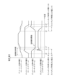
- FIG. 11 is a conceptual diagram of main waveforms when a low-side arm switching element is erroneously turned on when a low-side arm switching element is in a non-conducting state and a high-side arm switching element is in a conducting state in a half-bridge circuit in a power conversion device according to embodiment 1.
- 10A to 10C are main reference waveform conceptual diagrams when the switching times of the switching elements of the low-side arm and the high-side arm in a half-bridge circuit are not changed.
- 11 is a conceptual diagram of main reference waveforms when the switching element of the low-side arm is falsely turned on when the switching times of the switching elements of the low-side arm and the high-side arm in a half-bridge circuit are not changed and the switching element of the low-side arm is in a non-conducting state and the switching element of the high-side arm is in a conducting state.
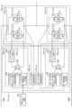
- 11 is a schematic configuration diagram mainly showing a half-bridge circuit, which is a one-phase bridge rectifier circuit of a three-phase bridge rectifier circuit in a power conversion device according to a second embodiment, and a part of a control circuit that controls the half-bridge circuit.
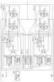
- FIG. 11 is a schematic configuration diagram mainly showing a half-bridge circuit, which is a one-phase bridge rectifier circuit of a three-phase bridge rectifier circuit in a power conversion device according to embodiment 3, and a part of a control circuit that controls the half-bridge circuit.
- a half-bridge circuit which is a one-phase bridge rectifier circuit of a three-phase bridge rectifier circuit in a power conversion device according to embodiment 3, and a part of a control circuit that controls the half-bridge circuit.
- Embodiment 1 A power conversion device according to a first embodiment will be described with reference to FIGS. 1 to 4.
- FIG. The power conversion device 300 according to the first embodiment is a power conversion device that receives input power from a power source, converts the input power, and outputs output power to a load.
- the power conversion device 300 according to the first embodiment specifically includes a power conversion circuit 10, which is a three-phase inverter circuit that converts DC power from a DC power source 100 serving as a power source into three-phase AC power, and supplies the three-phase AC power to a load 200.
- the following description will be focused mainly on a specific example including a power conversion circuit 10 that is a three-phase inverter circuit.
- the DC power supply 100 is, for example, a battery formed of a secondary battery such as a nickel-metal hydride battery or a lithium-ion battery.
- the DC power supply 100 is, for example, a battery used with a rated voltage ranging from about 1000V to 200V.
- the DC power supply 100 is designed to handle a high voltage of up to about 1000V. In the following description, the maximum voltage of about 1000 V among the rated voltages of the DC power supply 100 will be referred to as the set voltage.
- the positive electrode is electrically connected to the positive electrode input terminal 1P of the power conversion device 300
- the negative electrode is electrically connected to the negative electrode input terminal 1N of the power conversion device 300
- the DC power supply 100 supplies DC power to the power conversion device 300.
- the load 200 is, for example, a three-phase motor that drives the drive wheels of the electric vehicle or the hybrid vehicle.
- the U-phase input terminal is electrically connected to the u-phase output terminal 2U of the power conversion device 300
- the V-phase input terminal is electrically connected to the v-phase output terminal 2V of the power conversion device 300
- the W-phase input terminal is electrically connected to the w-phase output terminal 2W of the power conversion device 300
- the load 200 is supplied with three-phase AC power from the power conversion device 300.
- a power conversion device 300 includes a power conversion circuit 10, a smoothing capacitor 20, a control circuit unit 30, and a voltage sensor circuit 40.
- One electrode of the smoothing capacitor 20 is connected to a positive power supply wiring 50P that electrically connects the positive input terminal 1P of the power conversion device 300 and the positive input terminal 11P of the power conversion circuit 10, and the other electrode of the smoothing capacitor 20 is connected to a negative power supply wiring 50N that electrically connects the negative input terminal 1N of the power conversion device 300 and the negative input terminal 11N of the power conversion circuit 10.
- the smoothing capacitor 20 is a smoothing capacitor element for removing voltage ripples and noise in the positive power supply wiring 50P and the negative power supply wiring 50N.
- the power conversion circuit 10 is a switching circuit having a switching element for controlling power.
- the power conversion circuit 10 is a three-phase inverter circuit using a three-phase bridge rectifier circuit (three-phase full-wave rectifier circuit) constituted by switching elements 14u, 15u, 14v, 15v, 14w, and 15w.
- the switching elements 14u, 15u, 14v, 15v, 14w, and 15w each have a pair of main terminals and a control terminal, and are a semiconductor switching element group having a plurality of semiconductor switching elements connected in parallel.
- the pair of main terminals is a drain terminal and a source terminal
- the control terminal is a gate terminal.
- Each semiconductor switching element group is composed of two semiconductor switching elements connected in parallel and controlled to be turned on and off at the same timing by the same control signal.
- Each semiconductor switching element group may be composed of three or more semiconductor switching elements that are connected in parallel and controlled to be turned on and off at the same timing in order to output large power.
- the switching element 14u and the switching element 15u constitute a u-phase inverter section in a three-phase inverter circuit.
- the switching elements 14u and 15u are connected in series between the positive input terminal 11P and the negative input terminal 11N, and form a half-bridge circuit 13u, which is a u-phase bridge rectifier circuit, in which the connection point between the switching elements 14u and 15u becomes a u-phase output node 16u.
- Switching element 14v and switching element 15v constitute a v-phase inverter section in a three-phase inverter circuit.
- Switching element 14v and switching element 15v are connected in series between positive input terminal 11P and negative input terminal 11N, and form half-bridge circuit 13v, which is a v-phase bridge rectifier circuit, in which the connection point between switching element 14v and switching element 15v becomes v-phase output node 16v.
- the switching element 14w and the switching element 15w constitute a w-phase inverter section in the three-phase inverter circuit.
- Switching element 14w and switching element 15w are connected in series between positive input terminal 11P and negative input terminal 11N, and form half-bridge circuit 13w, which is a w-phase bridge rectifier circuit, in which the connection point between switching element 14w and switching element 15w becomes w-phase output node 16w.
- FIG. 2 shows the half-bridge circuits 13u, 13v, and 13w for one phase, and the control signal generating units 31u, 31v, and 31w for one phase of the control circuit unit 30 that controls the half-bridge circuits 13u, 13v, and 13w for one phase. Therefore, in the following description, the u-phase, v-phase and w-phase half-bridge circuits 13u, 13v, 13w and the control signal generating units 31u, 31v, 31w will be described with reference to FIG.
- the switching element 14u is a group of semiconductor switching elements arranged as a high-side arm in the u-phase half-bridge circuit 13u, and is electrically connected between the positive input terminal 11P and a u-phase output node 16u.
- the u-phase output node 16u is electrically connected to a u-phase output terminal 12u of the power conversion circuit 10 via a u-phase power supply wiring.
- the u-phase output terminal 12u is electrically connected to the u-phase output terminal 2U of the power conversion device 300 via a u-phase power supply wiring.
- the u-phase output terminal 2U is connected to the U-phase input terminal of a three-phase motor.
- the switching element 14u includes a semiconductor switching element 14u1 consisting of a transistor element Tr that operates as a semiconductor switching element and a free wheel diode D connected in anti-parallel to the transistor element Tr, and a semiconductor switching element 14u2 consisting of a transistor element Tr that operates as a semiconductor switching element and a free wheel diode D connected in anti-parallel to the transistor element Tr, and connected in parallel to the semiconductor switching element 14u1.
- the transistor element Tr of the semiconductor switching element 14u1 and the transistor element Tr of the semiconductor switching element 14u2 are turned on and off at the same timing by a control signal for the u-phase high side arm from the control circuit unit 30.
- the drain electrodes of the two transistor elements Tr are electrically connected to the positive input terminal 11P
- the source electrodes of the two transistor elements Tr are electrically connected to a u-phase output node 16u
- the gate electrodes of the two transistor elements Tr are electrically connected to an output node 34u of a control signal generating unit 32u for the high-side arm of a control signal generating unit 31u in the control circuit section 30.
- the switching element 15u is a group of semiconductor switching elements arranged as a low-side arm in the u-phase half-bridge circuit 13u, and is electrically connected between the u-phase output node 16u and the negative input terminal 11N. As shown in FIG.
- the switching element 15u includes a semiconductor switching element 15u1 consisting of a transistor element Tr operating as a semiconductor switching element and a diode element D connected in anti-parallel to the transistor element Tr and operating as a free-wheeling diode, and a semiconductor switching element 15u2 consisting of a transistor element Tr operating as a semiconductor switching element and a diode element D connected in anti-parallel to the transistor element Tr and operating as a free-wheeling diode, and connected in parallel to the semiconductor switching element 15u1.
- the transistor element Tr of the semiconductor switching element 15u1 and the transistor element Tr of the semiconductor switching element 15u2 are turned on and off at the same timing by a control signal for the u-phase low-side arm from the control circuit unit 30.
- the drain electrodes of the two transistor elements Tr are electrically connected to the u-phase output node 16u
- the source electrodes of the two transistor elements Tr are electrically connected to the negative input terminal 11N
- the gate electrodes of the two transistor elements Tr are electrically connected to an output node 35u of a control signal generating unit 33u for the low-side arm of a control signal generating unit 31u in the control circuit section 30.
- the two semiconductor switching elements 14u1 and 14u2 constituting the switching element 14u and the two semiconductor switching elements 15u1 and 15u2 constituting the switching element 15u have a 2-in-1 power module structure sealed with molding resin in the same package. Instead of sealing with a molding resin, sealing with a gel may be used.
- a u-phase half-bridge circuit (inverter unit) 13u having a power module structure has a gate terminal, a drain terminal, and a source terminal for a low-side arm, and a gate terminal, a drain terminal, and a source terminal for a high-side arm.
- the source terminal of the switching element 14u arranged in the high-side arm is located at a position equidistant from the source electrodes of the two transistor elements Tr
- the source terminal of the switching element 15u arranged in the low-side arm is located at a position equidistant from the source electrodes of the two transistor elements Tr.
- each of switching element 14u and switching element 15u may be configured as two semiconductor switching elements in a semiconductor module. Even in this case, the source terminal of switching element 14u is located equidistant from the source electrodes of the two transistor elements Tr, and the source terminal of switching element 15u is located equidistant from the source electrodes of the two transistor elements Tr.
- switching element 14u and switching element 15u are each configured with three or more semiconductor switching elements to output high power
- multiple power modules configured with the semiconductor switching elements of switching element 14u and the semiconductor switching elements of switching element 15u may be connected in parallel.
- switching element 14u and switching element 15u are each configured with three or more semiconductor switching elements to output high power
- switching element 14u may be configured with a power module in which multiple switching elements are connected in parallel
- switching element 15u may be configured with a power module in which multiple switching elements are connected in parallel.
- the switching element 14v is a group of semiconductor switching elements arranged as a high-side arm in the v-phase half-bridge circuit 13v, and is electrically connected between the positive input terminal 11P and the v-phase output node 16v.
- the v-phase output node 16v is electrically connected to the v-phase output terminal 12v of the power conversion circuit 10 via a v-phase power supply wiring.
- the v-phase output terminal 12v is electrically connected to the v-phase output terminal 2V of the power conversion device 300 via a v-phase power supply wiring.
- the v-phase output terminal 2V is connected to the V-phase input terminal of the three-phase motor.
- the switching element 14v includes a semiconductor switching element 14v1 consisting of a transistor element Tr that operates as a semiconductor switching element and a diode element D that is connected in anti-parallel to the transistor element Tr and operates as a free-wheeling diode, and a semiconductor switching element 14v2 that consists of a transistor element Tr that operates as a semiconductor switching element and a diode element D that is connected in anti-parallel to the transistor element Tr and operates as a free-wheeling diode and is connected in parallel to the semiconductor switching element 14v1.
- the transistor element Tr of the semiconductor switching element 14v1 and the transistor element Tr of the semiconductor switching element 14v2 are turned on and off at the same timing by a control signal for the v-phase high side arm from the control circuit unit 30.
- the drain electrodes of the two transistor elements Tr are electrically connected to the positive input terminal 11P
- the source electrodes of the two transistor elements Tr are electrically connected to a v-phase output node 16v
- the gate electrodes of the two transistor elements Tr are electrically connected to an output node 34v of a control signal generating section 32v for the high-side arm of a control signal generating section 31v in the control circuit section 30.
- the switching element 15v is a group of semiconductor switching elements arranged as a low-side arm in the v-phase half-bridge circuit 13v, and is electrically connected between the v-phase output node 16v and the negative input terminal 11N. As shown in FIG.
- the switching element 15v includes a semiconductor switching element 15v1 consisting of a transistor element Tr operating as a semiconductor switching element and a diode element D connected in anti-parallel to the transistor element Tr and operating as a free-wheeling diode, and a semiconductor switching element 15v2 consisting of a transistor element Tr operating as a semiconductor switching element and a diode element D connected in anti-parallel to the transistor element Tr and operating as a free-wheeling diode, and connected in parallel to the semiconductor switching element 15v1.
- the transistor element Tr of the semiconductor switching element 15v1 and the transistor element Tr of the semiconductor switching element 15v2 are turned on and off at the same timing by a control signal for the v-phase low-side arm from the control circuit unit 30.
- the drain electrodes of the two transistor elements Tr are electrically connected to a v-phase output node 16v
- the source electrodes of the two transistor elements Tr are electrically connected to the negative input terminal 11N
- the gate electrodes of the two transistor elements Tr are electrically connected to an output node 35v of a control signal generating section 33v for the low-side arm of a control signal generating section 31v in the control circuit section 30.
- the two semiconductor switching elements 14v1 and 14v2 constituting the switching element 14v and the two semiconductor switching elements 15v1 and 15v2 constituting the switching element 15v are sealed with molding resin in the same package to form a 2-in-1 power module structure.
- sealing with a molding resin sealing with a gel may be used.
- a v-phase half-bridge circuit (inverter section) 13v having a power module structure has a gate terminal, a drain terminal, and a source terminal for a low-side arm, and a gate terminal, a drain terminal, and a source terminal for a high-side arm.
- the source terminal of the switching element 14v arranged in the high-side arm is located at a position equidistant from the source electrodes of the two transistor elements Tr
- the source terminal of the switching element 15v arranged in the low-side arm is located at a position equidistant from the source electrodes of the two transistor elements Tr.
- switching element 14v and switching element 15v may each be configured with two semiconductor switching elements in a semiconductor module, similar to switching element 14. Even in this case, the source terminal of switching element 14v is located equidistant from the source electrodes of the two transistor elements Tr, and the source terminal of switching element 15v is located equidistant from the source electrodes of the two transistor elements Tr.
- switching element 14v and switching element 15v are each configured with three or more semiconductor switching elements to output high power
- switching element 14v may be configured with a power module in which multiple switching elements are connected in parallel
- switching element 15v may be configured with a power module in which multiple switching elements are connected in parallel.
- the switching element 14w is a group of semiconductor switching elements arranged as a high-side arm in the w-phase half-bridge circuit 13w, and is electrically connected between the positive input terminal 11P and the w-phase output node 16w.
- the w-phase output node 16w is electrically connected to the w-phase output terminal 12w of the power conversion circuit 10 via a w-phase power supply wiring.
- the w-phase output terminal 12w is electrically connected to the w-phase output terminal 2W of the power conversion device 300 via a w-phase power supply wiring.
- the w-phase output terminal 2W is connected to the W-phase input terminal of the three-phase motor.
- the switching element 14w includes a semiconductor switching element 14w1 consisting of a transistor element Tr that operates as a semiconductor switching element and a diode element D that is connected in anti-parallel to the transistor element Tr and operates as a free-wheeling diode, and a semiconductor switching element 14w2 consisting of a transistor element Tr that operates as a semiconductor switching element and a diode element D that is connected in anti-parallel to the transistor element Tr and operates as a free-wheeling diode and is connected in parallel to the semiconductor switching element 14w1.
- the transistor element Tr of the semiconductor switching element 14w1 and the transistor element Tr of the semiconductor switching element 14w2 are turned on and off at the same timing by a control signal for the w-phase high side arm from the control circuit unit 30.
- the drain electrodes of the two transistor elements Tr are electrically connected to the positive input terminal 11P
- the source electrodes of the two transistor elements Tr are electrically connected to a w-phase output node 16w
- the gate electrodes of the two transistor elements Tr are electrically connected to an output node 34w of a control signal generating section 32w for the high-side arm of a control signal generating section 31w in the control circuit section 30.
- the switching element 15w is a group of semiconductor switching elements arranged as a low-side arm in the w-phase half-bridge circuit 13w, and is electrically connected between the w-phase output node 16w and the negative input terminal 11N. As shown in FIG.
- the switching element 15w includes a semiconductor switching element 15w1 consisting of a transistor element Tr operating as a semiconductor switching element and a diode element D connected in anti-parallel to the transistor element Tr and operating as a free-wheeling diode, and a semiconductor switching element 15w2 consisting of a transistor element Tr operating as a semiconductor switching element and a diode element D connected in anti-parallel to the transistor element Tr and operating as a free-wheeling diode, and connected in parallel to the semiconductor switching element 15w1.
- the transistor element Tr of the semiconductor switching element 15 w 1 and the transistor element Tr of the semiconductor switching element 15 w 2 are turned on and off at the same timing by a control signal for the w-phase low-side arm from the control circuit unit 30 .
- the drain electrodes of the two transistor elements Tr are electrically connected to a w-phase output node 16w
- the source electrodes of the two transistor elements Tr are electrically connected to the negative input terminal 11N
- the gate electrodes of the two transistor elements Tr are electrically connected to an output node 35w of a control signal generating section 33w for the low-side arm of a control signal generating section 31w in the control circuit section 30.
- the two semiconductor switching elements 14w1 and 14w2 constituting the switching element 14w and the two semiconductor switching elements 15w1 and 15w2 constituting the switching element 15w are sealed with molding resin in the same package to form a 2-in-1 power module structure.
- sealing with a molding resin sealing with a gel may be used.
- a w-phase half-bridge circuit (inverter unit) 13w having a power module structure has a gate terminal, a drain terminal, and a source terminal for a low-side arm, and a gate terminal, a drain terminal, and a source terminal for a high-side arm.
- the source terminal of the switching element 14w arranged in the high-side arm is located at a position equidistant from the source electrodes of the two transistor elements Tr
- the source terminal of the switching element 15w arranged in the low-side arm is located at a position equidistant from the source electrodes of the two transistor elements Tr.
- switching element 14w and switching element 15w may each be configured with two semiconductor switching elements in a semiconductor module, similar to switching element 14. Even in this case, the source terminal of switching element 14w is located equidistant from the source electrodes of the two transistor elements Tr, and the source terminal of switching element 15w is located equidistant from the source electrodes of the two transistor elements Tr.
- switching element 14w and switching element 15w are each configured with three or more semiconductor switching elements to output high power
- multiple power modules configured with the semiconductor switching elements of switching element 14w and the semiconductor switching elements of switching element 15w may be connected in parallel.
- switching element 14w and switching element 15w are each configured with three or more semiconductor switching elements to output high power
- switching element 14w may be configured with a power module in which multiple switching elements are connected in parallel
- switching element 15w may be configured with a power module in which multiple switching elements are connected in parallel.
- the transistor elements Tr of the multiple semiconductor switching elements in the semiconductor switching element group constituting switching element 14u, the transistor elements Tr of the multiple semiconductor switching elements in the semiconductor switching element group constituting switching element 15u, the transistor elements Tr of the multiple semiconductor switching elements in the semiconductor switching element group constituting switching element 14v, the transistor elements Tr of the multiple semiconductor switching elements in the semiconductor switching element group constituting switching element 15v, the transistor elements Tr of the multiple semiconductor switching elements in the semiconductor switching element group constituting switching element 14w, and the transistor elements Tr of the multiple semiconductor switching elements in the semiconductor switching element group constituting switching element 15w are each wide bandgap semiconductor elements formed on a semiconductor substrate made of a material such as silicon, silicon carbide, or gallium nitride, using a wide bandgap semiconductor having a bandgap wider than that of silicon, for example silicon carbide or gallium nitride.
- semiconductor switching elements 14u1, 15u1, 14v1, 15v1, 14w1, and 15w1 and semiconductor switching elements 14u2, 15u2, 14v2, 15v2, 14w2, and 15w2 are power control semiconductor switching elements that are wide bandgap metal oxide semiconductor field effect transistors (MOSFETs).
- MOSFETs metal oxide semiconductor field effect transistors
- the diode element D which is connected inversely in parallel with the transistor element Tr and operates as a free wheeling diode is not configured separately for the transistor element Tr, but the parasitic diode of the MOSFET as the transistor element Tr functions as the free wheeling diode.
- a power control semiconductor switching element that is a wide band gap insulated gate bipolar transistor (IGBT) may be used.
- IGBT insulated gate bipolar transistor
- each semiconductor switching element has an IGBT that operates as a transistor element Tr and a wide band gap diode element that functions as a freewheeling diode D.
- the above-mentioned transistor elements Tr may each be replaced with other power control semiconductor switching elements such as bipolar transistors.
- the wide band gap semiconductor elements When wide band gap semiconductor elements are used as each of the semiconductor switching elements described above, the wide band gap semiconductor elements have high dielectric breakdown strength and are therefore suitable for a three-phase inverter circuit that constitutes the power conversion circuit 10, which processes high-voltage input voltages of up to about 1000V.
- the control circuit unit 30 acquires information about the input voltage in the power conversion device 300 from the voltage sensor circuit 40, and changes the switching times of the multiple semiconductor switching elements 14u1 and 14u2, 15u1 and 15u2, 14v1 and 14v2, 15v1 and 15v2, 14w1 and 14w2, and 15w1 and 15w2 in the semiconductor switching element groups that constitute each of the switching elements 14u, 15u, 14v, 15v, 14w, and 15w in accordance with the input voltage input to the power conversion circuit 10, and outputs control signals to control terminals of the multiple semiconductor switching elements in the semiconductor switching element groups to control on and off the multiple semiconductor switching elements in the semiconductor switching element groups.
- the reference numerals of the semiconductor switching elements in the semiconductor switching element group will be omitted unless a distinction is required in the explanation.
- control circuit unit 30 outputs a control signal for the low side arm and the high side arm of the u phase, a control signal for the low side arm and the high side arm of the v phase, and a control signal for the low side arm and the high side arm of the w phase in response to gate terminals, which are control terminals corresponding to the semiconductor switching element groups arranged in the low side arm and the high side arm of the u phase half bridge circuit (inverter unit) 13u, the low side arm and the high side arm of the v phase half bridge circuit (inverter unit) 13v, and the low side arm and the high side arm of the w phase half bridge circuit (inverter unit) 13w.
- the switching time is the time it takes to turn on and off a plurality of semiconductor switching elements 14u1 and 14u2, 15u1 and 15u2, 14v1 and 14v2, 15v1 and 15v2, 14w1 and 14w2, and 15w1 and 15w2 in the semiconductor switching element groups that constitute each of the switching elements 14u, 15u, 14v, 15v, 14w, and 15w.
- the control circuit unit 30 sets the input voltage input to the power conversion circuit 10 to 1000V, which is the maximum voltage of the DC power supply 100, sets a switching time that suppresses the occurrence of a surge due to the input voltage so that the withstand voltage of the semiconductor switching element at the set voltage is not exceeded, and outputs a control signal to the gate terminal of the semiconductor switching element when the input voltage input to the power conversion circuit 10 is lower than the set voltage, shortening the switching time to be shorter than the switching time for the set voltage.
- 1000V is the maximum voltage of the DC power supply 100
- the power conversion circuit 10 when the input voltage is lower than the set voltage, changes the control signal to one that shortens the switching time compared to the switching time of the control signal that controls the semiconductor switching element on and off using the same control signal as the control signal that controls the semiconductor switching element on and off using the switching time for the set voltage.
- the switching time is shortened by 15% or more with respect to the switching time for the set voltage.
- the reason why the threshold for switching the switching time is set at 400V is that the parasitic capacitance Cds between the drain and source of the semiconductor switching element fluctuates greatly, that is, has a large dependency when the drain-source voltage reaches about 400V.
- the switching time is switched between two stages, that is, a range in which the input voltage input to the power conversion circuit 10 exceeds 400 V and a range in which the input voltage is below 400 V
- the switching time may be divided into three or more stages, and the switching time may be shortened toward a range in which the input voltage becomes lower. That is, the voltage range of the input voltage input to the power conversion circuit 10 may be divided into a plurality of stages, and the switching time may be set to be shorter in a plurality of stages toward a range in which the input voltage becomes lower corresponding to the plurality of stages.
- the switching time may be changed from the switching time for a set voltage according to the input voltage so as to become continuously shorter as the input voltage decreases.
- the drain-source parasitic capacitance Cds becomes large, the drain-source current of the semiconductor switching element becomes large, and the current flowing through the gate electrode of the semiconductor switching element becomes large. Since the fluctuation in the gate-source voltage of the semiconductor switching element becomes large, the amount of change in the gate-source current also becomes large.
- a deviation may occur in the switching timing of the parallel-connected semiconductor switching elements.
- a deviation in switching timing occurs, a potential difference is generated between the potentials of the drain electrodes or between the potentials of the source electrodes of the semiconductor switching elements connected in parallel, causing a current to flow through the drain-source parasitic capacitance Cds of the semiconductor switching elements connected in parallel, and a part of the current flows into the gate electrode via the gate-drain parasitic capacitance Cgd and gate-source parasitic capacitance Cgs of the semiconductor switching element, causing a current to flow between the gate electrodes of the semiconductor switching elements connected in parallel.
- the switching time is changed to be shorter than the switching time for the set voltage, so that the state in which gate oscillation is likely to occur in the parallel-connected semiconductor switching elements that constitute the switching element, i.e., the switching operation can be escaped from before it reaches a large amplitude.
- the semiconductor switching element is turned on in a short switching time, and the drain-source of the semiconductor switching element is brought into a conductive state, so that the impedance of the channel portion of the semiconductor switching element becomes lower than the parasitic capacitance Cds between the drain and source of the semiconductor switching element.
- the exchange of charge via the parasitic capacitance Cds between the drain and source of the semiconductor switching elements connected in parallel no longer occurs, and the gate oscillation converges.
- wide band gap semiconductor elements with high dielectric breakdown strength at high voltages such as an input voltage of 1000 V are used as the semiconductor switching elements that make up switching elements 14u, 15u, 14v, 15v, 14w, and 15w
- wide band gap semiconductors have high transconductance and are generally prone to oscillation.
- the switching time is changed to be shorter than the switching time for the set voltage. Therefore, the switching operation can be terminated before the gate oscillation reaches a large amplitude, thereby preventing the occurrence of destruction due to the semiconductor switching element exceeding its withstand voltage. That is, it is suitable for the power conversion circuit 10 that uses wide band gap semiconductor elements as semiconductor switching elements.
- the control circuit section 30 has a u-phase control signal generating section 31u, a v-phase control signal generating section 31v, and a w-phase control signal generating section 31w.
- the u-phase, v-phase, and w-phase control signal generating units 31u, 31v, and 31w respectively have control signal generating units 32u, 32v, and 32w for the high-side arm and control signal generating units 33u, 33v, and 33w for the low-side arm, short-circuit detection units 36u, 36v, and 36w for the high-side arms of the u-phase, v-phase, and w-phase, and short-circuit detection units 37u, 37v, and 37w for the low-side arms of the u-phase, v-phase, and w-phase.
- the u-phase, v-phase, and w-phase control signal generating units 31u, 31v, and 31w have the same configuration, and therefore FIG. 2 shows the control signal generating unit for one phase.
- the subscripts u, v, and w of the symbols are omitted, but the explanation is of the configuration of each of the u-phase control signal generating unit 31u, the v-phase control signal generating unit 31v, and the w-phase control signal generating unit 31w.
- the control signal generating section 31 has a control signal generating section 32 for a high side arm, a control signal generating section 33 for a low side arm, a short circuit detecting section 36 for a high side arm, and a short circuit detecting section 37 for a low side arm.
- the high-side arm control signal generating unit 32 has a high-side arm drive voltage generating unit 321 , an on/off command signal generating unit 322 , a gate driver 323 , and a gate resistor 324 .
- the drive voltage generating unit 321 generates an ON drive voltage which is an H level potential for turning on the parallel-connected semiconductor switching elements 14 1 and 14 2 of the switching element 14, and an OFF drive voltage which is an L level potential for turning off the semiconductor switching elements 14 1 and 14 2 .
- the drive voltage generating section 321 sets the H level potential and the L level potential within the withstand voltage of the semiconductor switching elements 14 1 , 14 2 and within a range that does not affect the reliability of the gate structures of the semiconductor switching elements 14 1 , 14 2 .
- the relative amount of the switching drive voltage is several volts, and the absolute value of the drive voltage after switching is on the order of several tens of volts.
- the off drive voltage is set to a negative voltage having a potential direction opposite to that of the on drive voltage, erroneous firing of the wide band gap MOSFET can be prevented.
- the on/off command signal generating unit 322 generates an on/off command signal that instructs the semiconductor switching elements 14 1 , 14 2 connected in parallel of the switching element 14 of the on timing at which they start to turn on and the off timing at which they start to turn off.
- the gate driver 323 outputs a control signal for the high side arm, which is an on/off pulse consisting of an H level potential which is the on drive voltage from the drive voltage generating unit 321 and an L level potential which is the off drive voltage, based on the on drive voltage and off drive voltage from the drive voltage generating unit 321 and the on/off command signal from the on/off command signal generating unit 322, between the voltage output node OUT and the reference potential node RP.
- the reference potential node RP is electrically connected to the source terminal of the switching element 14 .
- the gate resistor 324 determines the time it takes to turn on and off the semiconductor switching elements 14 1 and 14 2 , that is, the switching time, depending on the resistance value.
- the semiconductor switching elements 14 1 and 14 2 are turned on and off by a high-side arm control signal from a gate driver 323 whose switching time is determined by a gate resistor 324 .
- One terminal of the gate resistor 324 is electrically connected to a voltage output node OUT of the gate driver 323, and the other terminal is electrically connected to the gate electrodes of the semiconductor switching elements 14-1 and 14-2 connected in parallel of the switching element 14 via an output node 34 of the control signal generating unit 32.
- the resistance value becomes lower than the resistance value for the set voltage.
- the gate resistor 324 switches its resistance value in response to the output signal of the voltage sensor circuit 40 .
- the resistance value of the gate resistor 324 is set to a set value by an output signal indicating the set voltage of the voltage sensor circuit 40, and the switching time of the semiconductor switching elements 14-1 and 14-2 is set to a set time.
- the resistance value is switched to a resistance value lower than the set value by an output signal indicating a voltage lower than the set voltage of the voltage sensor circuit 40, and the switching time of the semiconductor switching elements 14-1 and 14-2 is set to a time shorter than the set time.
- a control signal that results in a switching time that is shorter than the switching time of the semiconductor switching elements 14-1 and 14-2 when the resistance value is the set value is output from the other terminal of the gate resistor 324 to the gate electrodes of the semiconductor switching elements 14-1 and 14-2 .
- the low-side arm control signal generating unit 33 includes a low-side arm drive voltage generating unit 331 , an on/off command signal generating unit 332 , a gate driver 333 , and a gate resistor 334 .
- the drive voltage generating unit 331 generates an ON drive voltage which is an H level potential for turning on the parallel-connected semiconductor switching elements 15-1 and 15-2 of the switching element 15, and an OFF drive voltage which is an L level potential for turning off the semiconductor switching elements 15-1 and 15-2.
- the drive voltage generating unit 331 is set within the withstand voltage of the semiconductor switching elements 15 1 and 15 2 and within a range that does not affect the reliability of the gate structure of the semiconductor switching elements 15 1 and 15 2 .
- the relative amount of the switching drive voltage is several volts, and the absolute value of the drive voltage after switching is on the order of several tens of volts.
- the off drive voltage is set to a negative voltage having a potential direction opposite to that of the on drive voltage, erroneous firing of the wide band gap MOSFET can be prevented.
- the on/off command signal generating unit 332 generates an on/off command signal that instructs the semiconductor switching elements 15 1 , 15 2 connected in parallel of the switching element 15 of the on timing at which they start to turn on and the off timing at which they start to turn off.
- the gate driver 333 outputs a control signal for the low side arm, which is an on/off pulse consisting of an H level potential which is the on drive voltage from the drive voltage generating unit 331 and an L level potential which is the off drive voltage, based on the on drive voltage and off drive voltage from the drive voltage generating unit 331 and the on/off command signal from the on/off command signal generating unit 332, between the voltage output node OUT and the reference potential node RP.
- the reference potential node RP is electrically connected to the source terminal of the switching element 15 .
- the gate resistor 334 determines the time it takes to turn on and off the semiconductor switching elements 15 1 and 15 2 , that is, the switching time, depending on the resistance value.
- the semiconductor switching elements 15 1 and 15 2 are turned on and off by a control signal for a low-side arm from a gate driver 333 whose switching time is determined by a gate resistor 334 .
- One terminal of the gate resistor 334 is electrically connected to a voltage output node OUT of the gate driver 333, and the other terminal is electrically connected to the gate electrodes of the parallel-connected semiconductor switching elements 15-1 and 15-2 of the switching element 15 via an output node 35 of the control signal generating unit 33.
- the resistance value of the gate resistor 334 becomes lower than the resistance value for the set voltage.
- the gate resistor 334 switches its resistance value in response to the output signal of the voltage sensor circuit 40 .
- the resistance value of the gate resistor 334 is set to a set value by an output signal indicating the set voltage of the voltage sensor circuit 40, and the switching time of the semiconductor switching elements 15-1 and 15-2 is set to a set time.
- the resistance value is switched to a resistance value lower than the set value by an output signal of the voltage sensor circuit 40 indicating a voltage lower than the set voltage, and the switching time of the semiconductor switching elements 15-1 and 15-2 is set to a time shorter than the set time.
- a control signal that results in a switching time that is shorter than the switching time of semiconductor switching elements 15-1 and 15-2 when the resistance value is the set value is output from the other terminal of gate resistor 334 to the gate electrodes of semiconductor switching elements 15-1 and 15-2 .
- the high-side short-circuit detection unit 36 detects a short circuit when the switching elements 14 and 15 connected in series in the half-bridge circuit 13 simultaneously become conductive due to erroneous firing of the switching element 15, resulting in a short circuit, and outputs an OFF command to the ON/OFF command signal generation unit 322.
- the ON/OFF command signal generator 322 Upon receiving the OFF command, the ON/OFF command signal generator 322 causes the gate driver 323 to output an L-level potential, which is an OFF drive voltage, to the voltage output node OUT, forcibly changing the switching element 14 from a conductive state to a non-conductive state.
- the semiconductor switching elements 14 1 and 14 2 constituting the switching element 14 are turned off, the short-circuit current is cut off, and the switching elements 14 and 15 are protected from short circuits.
- the low-side short-circuit detection unit 37 detects a short circuit when the switching elements 14 and 15 connected in series in the half-bridge circuit 13 simultaneously become conductive due to erroneous firing of the switching element 14, resulting in a short circuit, and outputs an OFF command to the ON/OFF command signal generation unit 332.
- the ON/OFF command signal generator 332 Upon receiving the OFF command, the ON/OFF command signal generator 332 causes the gate driver 333 to output an L-level potential, which is an OFF drive voltage, to the voltage output node OUT, forcibly changing the switching element 15 from a conductive state to a non-conductive state.
- the semiconductor switching elements 15 1 and 15 2 constituting the switching element 15 are turned off, the short-circuit current is cut off, and the switching elements 14 and 15 are protected from short circuits.
- the short circuit detection unit 36 is configured using a DESAT method, which monitors the drain-source voltage of the switching element 14 to determine whether or not the switching elements 14 and 15 are in a short-circuited state, and outputs an off command signal to the on/off command signal generating unit 322 if it determines that the switching elements 14 and 15 are in a short-circuited state.
- the short circuit detection unit 37 is configured using a DESAT method, which monitors the drain-source voltage of the switching element 15 to determine whether or not the switching elements 14 and 15 are in a short circuited state, and outputs an off command signal to the on/off command signal generating unit 332 if it determines that the switching element 14 and switching element 15 are in a short circuited state.
- the short circuit detection units 36 and 37 have the same configuration, and are each composed of a DESAT type circuit having comparators 361, 371, threshold generation sources 362, 372, resistors 363, 373, diodes 364, 374, constant current sources 365, 375, switches 366, 376, and capacitors 367, 377, as shown in FIG. 3.
- comparators 361, 371, threshold generation sources 362, 372, resistors 363, 373, diodes 364, 374, constant current sources 365, 375, switches 366, 376, and capacitors 367, 377 as shown in FIG. 3.
- reference symbols are listed to avoid duplication of explanation, with 36* indicating the components of short circuit detection unit 36 and 37* indicating the components of short circuit detection unit 37.
- Comparators 361, 371 have one input terminal electrically connected to short circuit detection nodes 368, 378, the other input terminal electrically connected to threshold generation sources 362, 372, and output ends electrically connected to on/off command signal generators 322, 332. If the potential appearing at short circuit detection nodes 368, 378 is greater than the threshold value set by threshold generation sources 362, 372, it is determined that switching elements 14, 15 are in a short circuit state, and an off command signal is output to the output end.
- the series circuits of the resistors 363, 373 and the diodes 364, 374 are electrically connected between the short circuit detection nodes 368, 378 and the drain electrodes of the switching elements 14, 15 so that the anode electrodes of the diodes 364, 374 are located on the short circuit detection nodes 368, 378 side.
- the constant current sources 365 and 375 are electrically connected to short circuit detection nodes 368 and 378 via switches 366 and 376 .
- the switches 366 and 376 receive a mask time designation signal, and are off when the mask time designation signal indicates the mask time, and are on when the mask time designation signal indicates the lapse of the mask time.
- the constant current sources 365 and 375 supply constant currents to the short circuit detection nodes 368 and 378 .
- the capacitors 367 and 377 are electrically connected between the short circuit detection nodes 368 and 378 and the source electrodes of the switching elements 14 and 15 .
- the short-circuit detection unit 36 detects that the drain-source voltage of switching element 14 becomes lower than the threshold value set by threshold generation source 362 after the short-circuit detection time has elapsed.
- the mask time designation signal indicates the elapse of the mask time, and after the mask time has elapsed, capacitor 367 begins to be charged by a constant current from constant current source 365. However, since the amount of current discharged to the drain terminal of switching element 14 via the series combination of resistor 363 and diode 364 is set to be greater than the amount of current charged to capacitor 367, the potential of short circuit detection node 368 does not exceed the threshold value after the short circuit detection time has elapsed. As a result, the comparator 361 does not output an OFF command signal.
- switching element 14 and switching element 15 are short-circuited, that is, when switching element 14 is in a conductive state and switching element 15 begins to turn on due to erroneous firing or the like, even after the short-circuit detection time has elapsed, switching element 14 is in a conductive state and switching element 15 is in a conductive state due to erroneous firing or the like, so the drain-source voltage of switching element 14 is higher than the threshold value set by threshold generation source 362.
- the mask time designation signal indicates the elapse of the mask time and capacitor 367 begins to be charged by the constant current from constant current source 365
- the potential of short circuit detection node 368 exceeds the threshold value after the short circuit detection time has elapsed since the capacitor 367 is not discharged to the drain terminal of switching element 14 via the series combination of resistor 363 and diode 364.
- an OFF command signal is output from the comparator 361, and the control signal generating unit 32 which receives the OFF command signal forcibly switches the semiconductor switching elements 14-1 and 14-2 constituting the switching element 14 from the conductive state to the OFF state, thereby cutting off the short-circuit current and protecting the switching elements 14 and 15 from short circuits.
- the short-circuit detection unit 37 detects that after the short-circuit detection time has elapsed, the voltage between the drain and source of switching element 15 becomes lower than the threshold value set by threshold generation source 372.
- the mask time designation signal indicates the elapse of the mask time, and after the mask time has elapsed, capacitor 377 begins to be charged by a constant current from constant current source 375. However, since it is set so that the amount of current discharged to the drain terminal of switching element 15 via the series combination of resistor 373 and diode 374 is greater than the amount of current charged to capacitor 377, the potential of short circuit detection node 378 does not exceed the threshold value after the short circuit detection time has elapsed. As a result, the comparator 371 does not output an OFF command signal.
- switching element 14 and switching element 15 are short-circuited, that is, when switching element 15 is in a conductive state and switching element 14 begins to turn on due to erroneous firing or the like, even after the short-circuit detection time has elapsed, switching element 15 is in a conductive state and switching element 14 is in a conductive state due to erroneous firing or the like, so the drain-source voltage of switching element 15 is higher than the threshold value set by threshold generation source 372.
- the short circuit detection time is a range of time set starting from the time when the gate potentials of the switching elements 14, 15 rise, that is, the time when the gate-source voltage starts to rise; in the first embodiment, this is the sum of the mask time and the time until the capacitors 367, 377 are charged by the constant current from the constant current sources 365, 375 in the normal state and the potentials of the short circuit detection nodes 368, 378 reach the threshold value. It is preferable that the short circuit detection time is short so that the short circuit can be detected as quickly as possible.
- the short circuit detection time is linked to the switching times of the switching elements 14 and 15 .
- the short circuit detection time is the time from when the switching elements 14, 15 start to turn on until the drain-source voltage has sufficiently dropped during normal operation when the input voltage input to the power conversion circuit 10 is the set voltage and the switching elements 14, 15 are not short-circuited, in order to prevent erroneous detection when the drain-source voltage has not dropped sufficiently while the switching elements 14, 15 are turning on, and the short circuit detection units 36, 37 do not perform short circuit detection until the set time has elapsed.
- the voltage sensor circuit 40 is connected between the positive power supply wiring 50P and the negative power supply wiring 50N, detects the input voltage input to the power conversion circuit 10, and outputs an output signal to the control circuit unit 30 in accordance with the detected input voltage.
- the control circuit unit 30 outputs a control signal corresponding to the output signal of the voltage sensor circuit 40 to the switching elements 14 and 15 in the power conversion circuit 10 .
- the resistance value of the gate resistor 324 of the control signal generating unit 32 for the high side arm and the gate resistor 334 of the control signal generating unit 33 for the low side arm in the control circuit unit 30 that receives the output signal from the voltage sensor circuit 40 is changed according to the output signal from the voltage sensor circuit 40.
- the output signal from the voltage sensor circuit 40 consists of a signal indicating a high voltage in the range of 1000 V, which is the set voltage, when the input voltage input to the power conversion circuit 10 exceeds 400 V, and a signal indicating a low voltage of 400 V or less.
- the gate resistors 324 and 334 are set to a resistance value for a set voltage, and when the output signal indicates a low voltage, the gate resistors 324 and 334 are switched to a resistance value lower than the resistance value for the set voltage.
- the resistance values of gate resistor 324 and gate resistor 334 are resistance values for the set voltage
- the drain-source voltage of switching element 14, 15 that turns on at the end of the short circuit detection time is less than the short circuit detection threshold, and short circuit detection units 36, 37 do not detect a short circuit.
- the resistance values for the set voltage in gate resistor 324 and gate resistor 334 are set to a value that becomes a control signal when the switching time becomes such that the drain-source voltage of switching elements 14, 15 becomes less than the short circuit detection threshold at the end of the short circuit detection time when the input voltage is high.
- the switching time of switching elements 14, 15 that are turned on is shorter than the switching time of switching elements 14, 15 that are turned on when gate resistor 324 and gate resistor 334 have resistance values for the set voltage, and the state in which gate oscillation occurs in switching elements 14, 15 that are turned on, i.e., the switching operation can be escaped from before it reaches a large amplitude. That is, the resistance values for the set voltage in the gate resistors 324 and 334 are set to values that provide control signals for switching times that suppress gate oscillation when the input voltage is low.
- a control signal is output from the control circuit unit 30 control signal generating units 32, 33 so that the switching time of the switching elements 14, 15 to be turned on is set to a switching time that will not cause erroneous detection of a short circuit at the end of the short circuit detection time
- a control signal is output from the control circuit unit 30 control signal generating units 32, 33 so that the switching time of the switching elements 14, 15 to be turned on is changed to a switching time that suppresses gate oscillation.
- the horizontal axis represents time
- the solid line represents the waveform when the input voltage is high, 1000 V in the first embodiment
- the dashed line represents the waveform when the input voltage is low, 400 V in the first embodiment.
- t0 is the time when switching element 15 (low-side arm) starts to turn on, and is the time when current starts to flow between the drain and source of switching element 15
- t1 is the time when the drain-source voltage of switching element 15 becomes zero when the input voltage is low (end of mirror time)
- t1' is the time when the drain-source voltage of switching element 15 becomes zero when the input voltage is high (end of mirror time)
- t2 is the time when switching element 15 starts to turn off, and is the time when the drain-source voltage of switching element 15 starts to rise (start of mirror time)
- t3 is the time when switching element 15 completes turning off when the input voltage is low, and is the time when the drain-source current of switching element 15 becomes zero
- t3' is the time when switching element 15 completes
- the switching time of switching element 15 when the input voltage is a low voltage, the switching time of switching element 15 is the time from time t0 to time t1 when it operates from off to on, and the time from time t2 to time t3 when it operates from on to off. In addition, in the case of switching element 15, when the input voltage is a high voltage, the switching time of switching element 15 is the time from time t0 to time t1' when it operates from off to on, and the time from time t2 to time t3' when it operates from on to off.
- the Miller time which is the transition time of the voltage between the drain and source when the semiconductor switching element is switched, becomes longer depending on the input voltage when the input voltage is high compared to when the input voltage is low, and the switching time of the switching element 15 when the input voltage is high becomes longer than the switching time of the switching element 15 when the input voltage is low.
- the short circuit detection time is shortened so that short circuit detection can be performed quickly when the input voltage is low, and is also shortened when the input voltage is high because the same short circuit detection time is usually used as when the input voltage is low. The same applies when the switching element 14 is turned on, and erroneous detection of a short circuit occurs when the input voltage is high.
- the control signal generating unit 33 in the control circuit unit 30 when the input voltage is high, the control signal generating unit 33 in the control circuit unit 30 outputs to the switching element 15 a control signal that determines the switching time at which the drain-source voltage of the switching element 15 becomes less than the short circuit detection threshold at the end of the short circuit detection time when the switching element 15 is turned on, and when the input voltage is low, the control signal from the control signal generating unit 33 in the control circuit unit 30 is changed to output to the switching element 15 a control signal that determines the switching time at which gate oscillation is suppressed when the switching element 15 is turned on.
- the power conversion device of embodiment 1 prevents the occurrence of a surge in the switching element 15 that exceeds the withstand voltage when the input voltage is high, eliminating false detection of a short circuit, and also prevents malfunction of the switching element 15 due to gate oscillation or the switching element 15 exceeding the withstand voltage when the input voltage is low. The same applies when the switching element 14 is turned on.
- FIG. 4 shows waveforms of an operation in which, when switching element 14 (high side arm) is in a conductive state and switching element 15 (low side arm) is in a non-conductive state, switching element 15 erroneously turns on for some reason, high side short circuit detection unit 36 detects that switching elements 14 and 15 are in a short circuit state, outputs an off command signal to high side on/off command signal generation unit 322, and control signal generation unit 32 turns off switching element 14 for short circuit protection.
- the horizontal axis represents time
- the solid line represents the waveform when the input voltage is high, 1000 V in the first embodiment
- the dashed line represents the waveform when the input voltage is low, 400 V in the first embodiment.
- FIG. 4 is a diagram for explaining a phenomenon that occurs due to a difference in switching time
- the vertical axis direction is the same for both high and low input voltages.
- the switching element 15 erroneously starts to turn on, that is, the voltage between the gate and source of the switching element 15 starts to rise.
- the short circuit detection time starts from the time when the switching element 15 starts to turn on.
- the gate-source voltage of the switching element 15 rises gradually because the resistance value of the gate resistor 334 in the control signal generating unit 33 for the low-side arm is high and a control signal resulting in a long switching time is input to the gate electrode of the switching element 15, and the state in which the drain-source resistance value of the switching element 15 is high continues.
- the drain-source voltage of switching element 15 When the input voltage is high, the drain-source voltage of switching element 15 remains high, so the drain-source resistance of switching element 15 changes slowly until the short-circuit current flowing through switching elements 14 and 15 reaches its peak, and then drops toward zero from the peak of the short-circuit current.
- the drain-source voltage of switching element 14 is determined by the drain-source voltage of switching element 15 when switching element 14 and switching element 15 are short-circuited, and when the input voltage is high, the drain-source resistance of switching element 15 remains high, so that the voltage changes slowly. If the drain-source voltage of the switching element 14 exceeds the short circuit detection threshold when the short circuit detection time has elapsed, the short circuit detection unit 36 detects a short circuit.
- the control signal generator 32 starts to gate off the switching element 14 .
- the drain-source voltage of switching element 14 changes slowly until the short-circuit current flowing through switching elements 14 and 15 reaches its peak, and then rises toward the input voltage from when the short-circuit current reaches its peak.
- the resistance value of the gate resistor 324 in the control signal generating unit 32 for the high side arm is high, and a control signal that results in a long switching time is input to the gate electrode of the switching element 14, so that it takes a long time for the switching element 14 to turn off.
- the switching time of switching element 15 is the time it takes for switching element 15 to go from OFF to ON
- the switching time of switching element 14 is the time it takes for switching element 14 to go from ON to OFF.
- the switching times of switching elements 14 and 15 correspond to the time that begins when the short-circuit current (through current) flowing through switching elements 14 and 15 begins to flow and ends when it ends.
- switching element 15 When the input voltage is high, switching element 15 repeats gate oscillation many times, but the drain-source voltage of switching element 15 is high, the switching time is long, and the rise of the gate-source voltage of switching element 15 is gradual. Therefore, even if switching elements 14 and 15 are simultaneously placed in a conductive state due to erroneous firing of switching element 15 or the like, resulting in a short-circuit state, it is possible to prevent the occurrence of an excess of voltage resistance due to a surge. The same applies when switching element 14 and switching element 15 are simultaneously brought into a conductive state and short-circuited due to erroneous firing of switching element 14 or the like.
- the resistance value of the gate resistor 334 in the control signal generating unit 33 for the low-side arm is changed to a low value, and a control signal that results in a shorter switching time is input to the gate electrode of the switching element 15, so that the rise time is fast and the time until the switching element 15 is turned on is short.
- the switching time of the switching element 15 is shorter, so that the resistance value between the drain and source of the switching element 15 decreases quickly and the drain-source voltage of the switching element 15 falls quickly. Since the resistance value between the drain and source of switching element 15 decreases quickly, when switching element 14 and switching element 15 are short-circuited, the drain-source voltage of switching element 14, which is determined by the drain-source voltage of switching element 15, changes, i.e., falls, quickly when the input voltage is low.
- the short circuit detection unit 36 detects a short circuit.
- the control signal generator 32 starts to gate off the switching element 14 .
- the switching time of switching element 15 at this time is the time it takes for switching element 15 to go from off to on, and the switching time of switching element 14 is the time it takes for switching element 15 to go from on to off.
- the switching times of switching elements 14 and 15 correspond to the time that starts when the short-circuit current that flows through switching elements 14 and 15 starts to flow, and ends when the current stops flowing.
- switching element 15 When the input voltage is low, the number of times that gate oscillation is repeated in switching element 15 is small, and the switching operation of switching element 15 can be completed before the vibration due to gate oscillation becomes noticeable. Even if switching elements 14 and 15 are simultaneously brought into a conductive state and short-circuited due to erroneous firing of switching element 15 or the like, the gate oscillation of switching element 15 is suppressed. The same applies when switching element 14 and switching element 15 are simultaneously brought into a conductive state and short-circuited due to erroneous firing of switching element 14 or the like.
- the switching times of the switching elements 14 and 15 are set to a switching time at which no erroneous detection of short circuit occurs at the end of the short circuit detection time, and as a result, a control signal is output from the control circuit unit 30 control signal generating units 32 and 33, which is set to a time that starts when the short circuit current flows through the switching elements 14 and 15 and ends when the short circuit current flows.
- the switching times of the switching elements 14 and 15 are changed to a switching time that suppresses gate oscillation.
- a control signal is output from the control circuit unit 30 control signal generating units 32 and 33, which is set to a time that starts when the short circuit current flows through the switching elements 14 and 15 and ends when the short circuit current flows.
- the horizontal axis represents time
- the solid line represents the waveform when the input voltage is high, 1000V in the first embodiment
- the dashed line represents the waveform when the input voltage is low, 400V in the first embodiment.
- t00 is the time when the short-circuit current starts to flow through the switching elements 14 and 15
- t01 is the time when the short-circuit current becomes zero. The time from time t00 to time t01 corresponds to the switching time of the switching elements 14 and 15.
- the drain-source voltage of switching element 15 remains in a high drain-source state, so it changes slowly until the short-circuit current flowing through switching elements 14 and 15 reaches its peak, and then drops toward zero from the peak of the short-circuit current.
- the drain-source voltage of switching element 14 is determined by the drain-source voltage of switching element 15 when switching element 14 and switching element 15 are short-circuited, and changes slowly because the drain-source resistance of switching element 15 remains high, just as in the case where the input voltage is a high voltage. If the drain-source voltage of the switching element 14 exceeds the short circuit detection threshold when the short circuit detection time has elapsed, the short circuit detection unit 36 detects a short circuit.
- the control signal generation unit 32 begins to gate off the switching element 14.
- the voltage between the drain and source of the switching element 14 changes slowly until the short circuit current flowing through the switching elements 14 and 15 reaches its peak, and then rises toward the input voltage from the point where the short circuit current peaks.
- the gate-source voltage of the switching element 14 is high because the resistance value of the gate resistor 324 in the control signal generating unit 32 for the high side arm is high, and a control signal that results in a long switching time is input to the gate electrode of the switching element 14, so it takes a long time for the switching element 14 to turn off.
- the control signal generating unit 33 in the control circuit unit 30 when the input voltage is high, the control signal generating unit 33 in the control circuit unit 30 outputs to the switching element 15 a control signal that determines the switching time at which the drain-source voltage of the switching element 15 becomes less than the short circuit detection threshold at the end of the short circuit detection time when the switching element 15 is turned on, and when the input voltage is low, the control signal from the control signal generating unit 33 in the control circuit unit 30 is changed to output to the switching element 15 a control signal that determines the switching time at which gate oscillation is suppressed when the switching element 15 is turned on.
- the power conversion device of embodiment 1 prevents the occurrence of a surge in the switching element 15 that exceeds the withstand voltage when the input voltage is high, eliminating false detection of a short circuit, and also prevents malfunction of the switching element 15 due to gate oscillation or the switching element 15 exceeding the withstand voltage when the input voltage is low. The same applies when the switching element 14 is turned on.
- the resistance values of the gate resistor 324 of the control signal generating unit 32 for the high side arm and the gate resistor 334 of the control signal generating unit 33 for the low side arm in the control circuit unit 30 of the power conversion circuit 10 are switched to resistance values lower than the set value, and the switching times of the multiple semiconductor switching elements 14 1 , 14 2 , 15 1 , 15 2 in the semiconductor switching element group constituting the switching elements 14 and 15 are set to be shorter than the set time.
- the occurrence of breakdown of the multiple semiconductor switching elements 14 1 , 14 2 , 15 1 , 15 2 due to exceeding the withstand voltage is suppressed, and when the input voltage input to the power conversion circuit 10 is a voltage lower than the set voltage, the occurrence of breakdown of the multiple semiconductor switching elements 14 1 , 14 2 , 15 1 , 15 2 is suppressed.
- , 152 can be suppressed from oscillating when the transistors are turned on.
- the power conversion device 300 is not limited to a power conversion device having a three-phase inverter circuit that converts DC to three-phase AC, but may be a power conversion device having a single-phase inverter circuit that converts DC to single-phase AC, a power conversion device having a converter circuit that converts AC to DC, or a power conversion device having a DC-DC converter circuit that transforms voltage.
- the term "power conversion circuit” includes any of a three-phase inverter circuit, a single-phase inverter circuit, a converter circuit, and a DC-DC converter circuit.
- Embodiment 2 A power conversion device according to a second embodiment will be described with reference to FIG.
- the power conversion device 300 of embodiment 2 differs from the power conversion device 300 of embodiment 1 in that the switching time is adjusted by changing the resistance values of gate resistor 324 of control signal generating unit 32 for the high side arm and gate resistor 334 of control signal generating unit 33 for the low side arm in the control circuit unit 30 in accordance with the input voltage input to the power conversion circuit 10, whereas the power conversion device 300 of embodiment 2 adjusts the switching time by changing at least one of the drive voltages of the gate for turning on and the gate for turning off of the semiconductor switching elements in drive voltage generating unit 321 of control signal generating unit 32 for the high side arm and drive voltage generating unit 331 of control signal generating unit 33 for the low side arm in the control circuit unit 30 in accordance with the input voltage input to the power conversion circuit 10; otherwise, the power conversion device 300 is the same as the power conversion device 300 of embodiment 1.
- the resistance values of the gate resistors 324 and 334 are the same regardless
- the power conversion device 300 when the input voltage input to the power conversion circuit 10 is lower than the set voltage, the power conversion device 300 changes the on drive voltage to a voltage higher than the on drive voltage for the set voltage, and changes the off drive voltage to a voltage lower than the off drive voltage for the set voltage, thereby switching the absolute value of the off drive voltage by a large value.
- the drive voltage for turning on is high, the rise speed of the gate-source voltage of the semiconductor switching element becomes faster, and when the drive voltage for turning off is low, the fall speed of the gate-source voltage of the semiconductor switching element becomes faster. As a result, the switching time for the semiconductor switching element can be shortened.
- the drive voltage generation unit 321 sets the on drive voltage and the off drive voltage to set values based on an output signal indicating a set voltage that indicates a high voltage from the voltage sensor circuit 40, and sets the switching time of the semiconductor switching elements 14-1 and 14-2 to the set time.
- the on drive voltage is switched to a drive voltage higher than the set value and the off drive voltage is switched to a drive voltage lower than the set value based on an output signal indicating a voltage lower than the set voltage from the voltage sensor circuit 40, and as a result, the switching time of the semiconductor switching elements 14-1 and 14-2 is set to a time shorter than the set time.
- the on drive voltage and the off drive voltage are set to set values by an output signal indicating a set voltage indicating a high voltage from the voltage sensor circuit 40, and the switching time of the semiconductor switching elements 15-1 , 15-2 is set to the set time.
- the on drive voltage is switched to a drive voltage higher than the set value and the off drive voltage is switched to a drive voltage lower than the set value by an output signal indicating a voltage lower than the set voltage from the voltage sensor circuit 40, and as a result, the switching time of the semiconductor switching elements 15-1 , 15-2 is set to a time shorter than the set time.
- the MOSFETs When wide band gap MOSFETs are used as the semiconductor switching elements 14-1 , 14-2 , the MOSFETs perform high speed switching operations, and therefore the transition speed dv/dt of the drain-source voltage during switching is large.
- the current flowing through the gate of the MOSFET which is generated by the parasitic capacitance Cdg ⁇ dv/dt, charges the parasitic capacitance Cgs, causing the gate-source voltage to rise, making it easy for false firing to occur.
- the off drive voltage is a negative voltage having a potential direction opposite to that of the on drive voltage, and the input voltage input to the power conversion circuit 10 is lower than the set voltage, the off drive voltage can be switched to a significantly lower drive voltage, thereby making it possible to set the switching time shorter than the set time without the MOSFET generating false firing.
- the ON drive voltage of the semiconductor switching elements in the drive voltage generating unit 321 of the control signal generating unit 32 for the high side arm and the drive voltage generating unit 331 of the control circuit unit 30 for the low side arm in the power conversion circuit 10 is changed to a value higher than the set voltage for the ON gate, or the OFF drive voltage is changed to a value lower than the set voltage for the OFF gate, or the ON drive voltage is switched to a value higher and the OFF drive voltage is switched to a value lower, in response to an output signal indicating that the input voltage input to the power conversion circuit 10 is lower than the set voltage . 2 exceeds the withstand voltage, and when the input voltage input to the power conversion circuit 10 is lower than a set voltage, gate oscillation can be suppressed when the multiple semiconductor switching elements 14 1 , 14 2 , 15 1 , 15 2 are turned on.
- the power conversion device 300 according to the second embodiment is used as a power conversion device for an electric powertrain such as a hybrid vehicle or an electric vehicle
- a lead-acid battery which is a DC power source for operating auxiliary devices of the hybrid vehicle or the electric vehicle may be used as the DC power source 100
- a flyback power source which receives as input a voltage supplied from the lead-acid battery as a driving power source for the control circuit unit 30 may be used as the driving voltage generation unit 321 and the driving voltage generation unit 331.
- the duty ratio of the flyback power supply can be changed in response to the output signal from the voltage sensor circuit 40, thereby achieving a change in the drive voltage.
- Embodiment 3 A power conversion device according to a third embodiment will be described with reference to FIG.
- the power conversion device 300 of embodiment 3 differs from the power conversion device of embodiment 1 in that the short circuit detection times in the high side short circuit detection unit 36 and the low side short circuit detection unit 37 are changed according to the input voltage input to the power conversion circuit 10, but is otherwise the same as the power conversion device 300 of embodiment 1.
- the same reference numerals as those in FIGS. 1 to 3 designate the same or corresponding parts.
- the short circuit detection time is set to a time at which a short circuit can be detected at the time when "short circuit detection (gate resistance: large)" is indicated
- the short circuit detection time is set to a time at which a short circuit can be detected at the time when "short circuit detection (gate resistance: large)" is indicated.
- Both short circuit detection times are times during which no erroneous detection of a short circuit occurs when switching element 14 and switching element 15 operate normally. That is, when switching element 14 and switching element 15 are turned on by normal operation, the drain-source voltage of switching element 14 and the drain-source voltage of switching element 15 become lower than the threshold voltage when the short circuit detection time has elapsed.
- high side short circuit detection unit 36 determines that switching element 14 and switching element 15 are in a short circuit state and outputs an off command signal to high side on/off command signal generation unit 322, causing control signal generation unit 32 to start an operation to turn off switching element 14 for short circuit protection.
- the switching element 14 since the switching element 14 starts its off operation earlier, the short-circuit time between the switching element 14 and the switching element 15 is shortened, and the switching operation of the switching element 15 can be completed before the vibration due to the gate oscillation becomes noticeable. The same applies if the switching element 14 is erroneously turned on.
- the switching time of switching element 15 is the time it takes for switching element 15 to go from off to on
- the switching time of switching element 14 is the time it takes for switching element 15 to go from on to off.
- the switching times of switching elements 14 and 15 correspond to the time from when the short-circuit current (through current) that flows through switching elements 14 and 15 starts to flow to when it ends.
- the short circuit detection units 36 and 37 are configured by a DESAT type circuit as shown in FIG. 3, and at least one of the mask time of the mask time designation signal, the current value of the constant current sources 365, 375, the threshold value of the threshold generation sources 362, 372, the capacitance value of the capacitors 367, 377, and the resistance value of the resistors 363, 373 is variable.
- the switching to shorten the short circuit detection time is performed by any one or a combination of shortening the mask time of the mask time designation signal input to the switches 366, 396, increasing the current value of the constant current sources 365, 375, lowering the threshold value of the threshold generation sources 362, 372, decreasing the capacitance of the capacitors 367, 377, and/or increasing the resistance value of the resistors 363, 373.
- the short circuit detection time until the short circuit detection unit 36 outputs an off command signal is shortened due to an output signal indicating that the input voltage input to the power conversion circuit 10 is lower than the set voltage, and in the event of a short circuit between switching element 14 and switching element 15, the short circuit time between switching element 14 and switching element 15 is shortened, thereby more reliably suppressing gate oscillation when multiple semiconductor switching elements 14-1 , 14-2 , 15-1 , and 15-2 are erroneously turned on.
- the short circuit detection time in the high side short circuit detection unit 36 and the low side short circuit detection unit 37 may be changed depending on the input voltage input to the power conversion circuit 10.
- gate oscillation that occurs when the plurality of semiconductor switching elements 14 1 , 14 2 , 15 1 , and 15 2 are erroneously turned on can be more reliably suppressed.
- the power conversion device according to the present disclosure is suitable for use in power conversion devices for electric powertrains such as hybrid vehicles or electric vehicles, for example, high-power inverters or converters.
Landscapes
- Engineering & Computer Science (AREA)
- Power Engineering (AREA)
- Inverter Devices (AREA)
- Power Conversion In General (AREA)
Abstract
電力変換装置は、電源(100)からの入力電力が入力され、入力された入力電力を電力変換して負荷(200)に出力電力を出力する電力変換装置(300)であって、制御端子をそれぞれが有し、並列接続された複数の半導体スイッチング素子を有する半導体スイッチング素子群(14u)、(15u)、(14v)、(15v)、(14w)、(15w)を具備する電力変換回路(10)と、電力変換回路(10)に入力される入力電圧に応じて半導体スイッチング素子群における複数の半導体スイッチ素子のスイッチング時間を変更して半導体スイッチング素子群(14u)、(15u)、(14v)、(15v)、(14w)、(15w)における複数の半導体スイッチ素子をオンオフ制御する制御信号を半導体スイッチング素子群(14u)、(15u)、(14v)、(15v)、(14w)、(15w)における複数の半導体スイッチ素子の制御端子に出力する制御回路部(30)と、を備える。
Description
本開示は、パワーエレクトロニクス分野のインバータまたはコンバータなどの電力変換装置に関する。
近年、ハイブリッド自動車または電気自動車などの電動パワートレイン用の電力変換装置は、スイッチング素子としてIGBT(Insulated Gate Bipolar Transistor)またはMOSFET(Metal Oxide Semiconductor Field Effect Transistor)などの半導体スイッチング素子が用いられ、大きい電力を処理するために、複数の半導体スイッチング素子を並列接続されたスイッチング素子が用いられる。
電力変換器における電圧コンバータのスイッチング素子として並列接続された2個の半導体スイッチング素子を、ゲート発振を抑えるために半導体モジュールとした例が特許文献1に示されている。
特許文献1に示された半導体モジュールは、一対の金属板と2個のトランジスタチップを備え、トランジスタチップは、一対の金属板に挟まれつつ、樹脂パッケージに封止されている。トランジスタチップのエミッタ電極は他方の金属板と導通している。樹脂パッケージの内部にて一方の金属板から2個のコレクタ端子が延びており、他方の金属板から1個のエミッタ端子が延びており、エミッタ端子はパッケージ側面にて2個のコレクタ端子の間から外部へ延びている。エミッタ端子は2個のトランジスタチップのそれぞれのエミッタ電極から等距離の位置で他方の金属板から延びている。
特許文献1に示された半導体モジュールは、一対の金属板と2個のトランジスタチップを備え、トランジスタチップは、一対の金属板に挟まれつつ、樹脂パッケージに封止されている。トランジスタチップのエミッタ電極は他方の金属板と導通している。樹脂パッケージの内部にて一方の金属板から2個のコレクタ端子が延びており、他方の金属板から1個のエミッタ端子が延びており、エミッタ端子はパッケージ側面にて2個のコレクタ端子の間から外部へ延びている。エミッタ端子は2個のトランジスタチップのそれぞれのエミッタ電極から等距離の位置で他方の金属板から延びている。
発明者らは、同じタイミングでオンオフ動作される2個の半導体スイッチング素子が並列接続されたスイッチング素子において、ドレイン-ソース間にかかる電圧、つまり、インバータまたはコンバータに入力されるなどの電力変換装置の電力変換回路に入力される入力電圧に相当する電圧を種々変化させたところ、次のような課題があることが判明した。
すなわち、ドレイン-ソース間にかかる電圧が高い範囲において、半導体スイッチング素子は耐圧に対するサージの許容値が小さいため、半導体スイッチング素子をオンオフ制御するスイッチング時間を長くする。
ドレイン-ソース間にかかる電圧が低い範囲において、ドレイン-ソース間にかかる電圧が高い範囲と同じスイッチング時間により半導体スイッチング素子をオンオフ制御するとゲート発振が大きな振幅となりやすく、大きな振幅のゲート発振が発生すると、スイッチング素子の誤動作または半導体スイッチング素子の耐圧超過による破壊の発生の恐れがあった。
ドレイン-ソース間にかかる電圧が低い範囲において、ドレイン-ソース間にかかる電圧が高い範囲と同じスイッチング時間により半導体スイッチング素子をオンオフ制御するとゲート発振が大きな振幅となりやすく、大きな振幅のゲート発振が発生すると、スイッチング素子の誤動作または半導体スイッチング素子の耐圧超過による破壊の発生の恐れがあった。
半導体スイッチング素子のドレイン-ソース間の寄生容量はドレイン-ソース間にかかる電圧が低い電圧であるほど大きくなり、ドレイン-ソース間の寄生容量が大きいほど、2個の半導体スイッチング素子間に流れる電流量が大きくなり、ゲート発振は大きな振幅となりやすいことに起因している。
一方、ドレイン-ソース間にかかる電圧が低い範囲において、ゲート発振の振幅がスイッチング素子の誤動作または半導体スイッチング素子の耐圧超過にならない短いスイッチング時間とする。
ドレイン-ソース間にかかる電圧が高い範囲において、ドレイン-ソース間にかかる電圧が低い範囲と同じスイッチング時間により半導体スイッチング素子をオンオフ制御するとサージによる耐圧超過が発生する。
ドレイン-ソース間にかかる電圧が高い範囲において、ドレイン-ソース間にかかる電圧が低い範囲と同じスイッチング時間により半導体スイッチング素子をオンオフ制御するとサージによる耐圧超過が発生する。
本開示は上記した点に鑑みてなされたものであり、電力変換回路が具備する、並列接続された複数の半導体スイッチング素子を有する半導体スイッチング素子群において発生するゲート発振を抑制する電力変換装置を得ることを目的とする。
本開示に係る電力変換装置は、電源からの入力電力が入力され、入力された入力電力を電力変換して負荷に出力電力を出力する電力変換装置であって、制御端子をそれぞれが有し、並列接続された複数の半導体スイッチング素子を有する半導体スイッチング素子群を具備する電力変換回路と、電力変換回路に入力される入力電圧に応じて半導体スイッチング素子群における複数の半導体スイッチ素子のスイッチング時間を変更して半導体スイッチング素子群における複数の半導体スイッチ素子をオンオフ制御する制御信号を半導体スイッチング素子群における複数の半導体スイッチ素子の制御端子に出力する制御回路部と、を備える。
本開示によれば、電力変換回路に入力される入力電圧に応じて半導体スイッチング素子群における複数の半導体スイッチング素子のスイッチング時間を変更して半導体スイッチング素子群における複数の半導体スイッチング素子を同時にオンオフ制御するので、半導体スイッチング素子群において発生するゲート発振を抑制することができる。
実施の形態1.
実施の形態1に係る電力変換装置を図1から図4を用いて説明する。
実施の形態1に係る電力変換装置300は電源からの入力電力が入力され、入力された入力電力を電力変換して負荷に出力電力を出力する電力変換装置である。
実施の形態1に係る電力変換装置300は、具体的には電源となる直流電源100からの直流電力を三相交流電力に変換する三相のインバータ回路である電力変換回路10を備え、三相交流電力を負荷200に供給する。
以下、三相のインバータ回路である電力変換回路10を備える具体例を対象に主として説明する。
実施の形態1に係る電力変換装置を図1から図4を用いて説明する。
実施の形態1に係る電力変換装置300は電源からの入力電力が入力され、入力された入力電力を電力変換して負荷に出力電力を出力する電力変換装置である。
実施の形態1に係る電力変換装置300は、具体的には電源となる直流電源100からの直流電力を三相交流電力に変換する三相のインバータ回路である電力変換回路10を備え、三相交流電力を負荷200に供給する。
以下、三相のインバータ回路である電力変換回路10を備える具体例を対象に主として説明する。
直流電源100は、電力変換装置300が電気自動車またはハイブリッド自動車に適用された場合は、例えば、ニッケル水素電池またはリチウムイオン電池等の二次電池からなるバッテリである。
直流電源100は、例えば1000V程度から200Vまでの範囲の定格電圧で使用されるバッテリである。
直流電源100は、特に高電圧対応である最大1000V程度の電圧を想定している。
直流電源100の定格電圧の内の最大電圧である1000V程度を以下の説明において設定電圧という。
直流電源100は、例えば1000V程度から200Vまでの範囲の定格電圧で使用されるバッテリである。
直流電源100は、特に高電圧対応である最大1000V程度の電圧を想定している。
直流電源100の定格電圧の内の最大電圧である1000V程度を以下の説明において設定電圧という。
直流電源100において、正電極が電力変換装置300の正極側の入力端子1Pに、負電極が電力変換装置300の負極側の入力端子1Nにそれぞれ電気的に接続され、直流電源100が電力変換装置300に直流電力を供給する。
負荷200は、電力変換装置300が電気自動車またはハイブリッド自動車に適用された場合は、例えば、電気自動車またはハイブリッド自動車の駆動輪を駆動する電動機である三相モータである。
負荷200は、電力変換装置300が電気自動車またはハイブリッド自動車に適用された場合は、例えば、電気自動車またはハイブリッド自動車の駆動輪を駆動する電動機である三相モータである。
負荷200において、U相の入力端子が電力変換装置300のu相の出力端子2Uに、V相の入力端子が電力変換装置300のv相の出力端子2Vに、W相の入力端子が電力変換装置300のw相の出力端子2Wにそれぞれ電気的に接続され、負荷200は電力変換装置300から三相の交流電力が供給される。
実施の形態1に係る電力変換装置300は、図1に示すように、電力変換回路10と平滑用コンデンサ20と制御回路部30と電圧センサ回路40を備える。
平滑用コンデンサ20の一方の電極が電力変換装置300の正極側の入力端子1Pと電力変換回路10の正極側の入力端子11Pとを電気的に接続する正極側の電源用配線50Pに接続され、平滑用コンデンサ20の他方の電極が電力変換装置300の負極側の入力端子1Nと電力変換回路10の負極側の入力端子11Nとを電気的に接続する負極側の電源用配線50Nに接続される。
平滑用コンデンサ20は正極側の電源用配線50Pおよび負極側の電源用配線50Nにおける電圧リプルおよびノイズ除去用の平滑用コンデンサ素子である。
平滑用コンデンサ20の一方の電極が電力変換装置300の正極側の入力端子1Pと電力変換回路10の正極側の入力端子11Pとを電気的に接続する正極側の電源用配線50Pに接続され、平滑用コンデンサ20の他方の電極が電力変換装置300の負極側の入力端子1Nと電力変換回路10の負極側の入力端子11Nとを電気的に接続する負極側の電源用配線50Nに接続される。
平滑用コンデンサ20は正極側の電源用配線50Pおよび負極側の電源用配線50Nにおける電圧リプルおよびノイズ除去用の平滑用コンデンサ素子である。
電力変換回路10は電力を制御するためのスイッチング素子を有するスイッチング回路である。
電力変換回路10は、実施の形態1ではスイッチング素子14u、15u、14v、15v、14w、15wにより構成される三相のブリッジ整流回路(三相の全波整流回路)による三相のインバータ回路である。
電力変換回路10は、実施の形態1ではスイッチング素子14u、15u、14v、15v、14w、15wにより構成される三相のブリッジ整流回路(三相の全波整流回路)による三相のインバータ回路である。
スイッチング素子14u、15u、14v、15v、14w、15wは、一対の主端子と制御端子をそれぞれが有し、並列接続された複数の半導体スイッチング素子を有する半導体スイッチング素子群である。
実施の形態1において、一対の主端子はドレイン端子およびソース端子であり、制御端子はゲート端子である。
各半導体スイッチング素子群は同じ制御信号により同じタイミングでオンオフ制御される2個の並列接続された半導体スイッチング素子により構成されている。
実施の形態1において、一対の主端子はドレイン端子およびソース端子であり、制御端子はゲート端子である。
各半導体スイッチング素子群は同じ制御信号により同じタイミングでオンオフ制御される2個の並列接続された半導体スイッチング素子により構成されている。
半導体スイッチング素子は、ゲート電極にオン用の駆動電圧であるHレベルの電位が印加されるとオン状態、つまりドレイン電極とソース電極の間が導通状態になり、ゲート電極にオフ用の駆動電圧であるLレベルの電位が印加されるとオフ状態、つまりドレイン電極とソース電極の間が非導通状態になる。
なお、各半導体スイッチング素子群は、大電力を出力するために並列接続された同じタイミングでオンオフ制御される3個以上の半導体スイッチング素子により構成されていてもよい。
なお、各半導体スイッチング素子群は、大電力を出力するために並列接続された同じタイミングでオンオフ制御される3個以上の半導体スイッチング素子により構成されていてもよい。
スイッチング素子14uとスイッチング素子15uは三相のインバータ回路におけるu相のインバータ部を構成する。
スイッチング素子14uとスイッチング素子15uは、正極側の入力端子11Pと負極側の入力端子11Nとの間に直列接続され、スイッチング素子14uとスイッチング素子15uの接続点がu相の出力ノード16uとなるu相のブリッジ整流回路であるハーフブリッジ回路13uを構成する。
スイッチング素子14uとスイッチング素子15uは、正極側の入力端子11Pと負極側の入力端子11Nとの間に直列接続され、スイッチング素子14uとスイッチング素子15uの接続点がu相の出力ノード16uとなるu相のブリッジ整流回路であるハーフブリッジ回路13uを構成する。
スイッチング素子14vとスイッチング素子15vは三相のインバータ回路におけるv相のインバータ部を構成する。
スイッチング素子14vとスイッチング素子15vは、正極側の入力端子11Pと負極側の入力端子11Nとの間に直列接続され、スイッチング素子14vとスイッチング素子15vの接続点がv相の出力ノード16vとなるv相のブリッジ整流回路であるハーフブリッジ回路13vを構成する。
スイッチング素子14vとスイッチング素子15vは、正極側の入力端子11Pと負極側の入力端子11Nとの間に直列接続され、スイッチング素子14vとスイッチング素子15vの接続点がv相の出力ノード16vとなるv相のブリッジ整流回路であるハーフブリッジ回路13vを構成する。
スイッチング素子14wとスイッチング素子15wは三相のインバータ回路におけるw相のインバータ部を構成する。
スイッチング素子14wとスイッチング素子15wは、正極側の入力端子11Pと負極側の入力端子11Nとの間に直列接続され、スイッチング素子14wとスイッチング素子15wの接続点がw相の出力ノード16wとなるw相のブリッジ整流回路であるハーフブリッジ回路13wを構成する。
スイッチング素子14wとスイッチング素子15wは、正極側の入力端子11Pと負極側の入力端子11Nとの間に直列接続され、スイッチング素子14wとスイッチング素子15wの接続点がw相の出力ノード16wとなるw相のブリッジ整流回路であるハーフブリッジ回路13wを構成する。
なお、電力変換回路10を構成する三相のインバータ回路におけるu相、v相、およびw相のハーフブリッジ回路13u、13v、13wがそれぞれ同様の構成であるので、図2は一相分のハーフブリッジ回路13u、13v、13wと一相分のハーフブリッジ回路13u、13v、13wを制御する制御回路部30の一相分の制御信号発生部31u、31v、31wを示している。
従って、以下の説明において、u相、v相、およびw相のハーフブリッジ回路13u、13v、13wおよび制御信号発生部31u、31v、31wそれぞれを説明するにあたり図2を用いて説明する。
従って、以下の説明において、u相、v相、およびw相のハーフブリッジ回路13u、13v、13wおよび制御信号発生部31u、31v、31wそれぞれを説明するにあたり図2を用いて説明する。
スイッチング素子14uはu相のハーフブリッジ回路13uにおけるハイサイドアームとして配置される半導体スイッチング素子群であり、正極側の入力端子11Pとu相の出力ノード16uの間に電気的に接続される。
u相の出力ノード16uは、電力変換回路10のu相の出力端子12uにu相の電源用配線を介して電気的に接続される。
u相の出力端子12uはu相の電源用配線を介して電力変換装置300のu相の出力端子2Uに電気的に接続される。
u相の出力端子2Uは三相モータのU相の入力端子に接続される。
u相の出力ノード16uは、電力変換回路10のu相の出力端子12uにu相の電源用配線を介して電気的に接続される。
u相の出力端子12uはu相の電源用配線を介して電力変換装置300のu相の出力端子2Uに電気的に接続される。
u相の出力端子2Uは三相モータのU相の入力端子に接続される。
スイッチング素子14uは、図2に示すように、半導体スイッチング素子として動作するトランジスタ素子Trとトランジスタ素子Trと逆並列に接続される還流ダイオードDからなる半導体スイッチング素子14u1と、半導体スイッチング素子として動作するトランジスタ素子Trとトランジスタ素子Trと逆並列に接続される還流ダイオードDからなり、半導体スイッチング素子14u1と並列接続された半導体スイッチング素子14u2とを有する。
半導体スイッチング素子14u1のトランジスタ素子Trと半導体スイッチング素子14u2のトランジスタ素子Trは制御回路部30からのu相のハイサイドアーム用の制御信号により同じタイミングでオンオフ動作する。
スイッチング素子14uにおいて、2個のトランジスタ素子Trのドレイン電極は正極側の入力端子11Pに電気的に接続され、2個のトランジスタ素子Trのソース電極はu相の出力ノード16uに電気的に接続され、2個のトランジスタ素子Trのゲート電極は制御回路部30における制御信号発生部31uのハイサイドアーム用の制御信号発生部32uの出力ノード34uに電気的に接続される。
スイッチング素子14uにおいて、2個のトランジスタ素子Trのドレイン電極は正極側の入力端子11Pに電気的に接続され、2個のトランジスタ素子Trのソース電極はu相の出力ノード16uに電気的に接続され、2個のトランジスタ素子Trのゲート電極は制御回路部30における制御信号発生部31uのハイサイドアーム用の制御信号発生部32uの出力ノード34uに電気的に接続される。
スイッチング素子15uはu相のハーフブリッジ回路13uにおけるローサイドアームとして配置される半導体スイッチング素子群であり、u相の出力ノード16uと負極側の入力端子11Nの間に電気的に接続される。
スイッチング素子15uは、図2に示すように、半導体スイッチング素子として動作するトランジスタ素子Trとトランジスタ素子Trと逆並列に接続され、環流ダイオードとして動作するダイオード素子Dとからなる半導体スイッチング素子15u1と、半導体スイッチング素子として動作するトランジスタ素子Trとトランジスタ素子Trと逆並列に接続され、環流ダイオードとして動作するダイオード素子Dとからなり、半導体スイッチング素子15u1と並列接続された半導体スイッチング素子15u2とを有する。
スイッチング素子15uは、図2に示すように、半導体スイッチング素子として動作するトランジスタ素子Trとトランジスタ素子Trと逆並列に接続され、環流ダイオードとして動作するダイオード素子Dとからなる半導体スイッチング素子15u1と、半導体スイッチング素子として動作するトランジスタ素子Trとトランジスタ素子Trと逆並列に接続され、環流ダイオードとして動作するダイオード素子Dとからなり、半導体スイッチング素子15u1と並列接続された半導体スイッチング素子15u2とを有する。
半導体スイッチング素子15u1のトランジスタ素子Trと半導体スイッチング素子15u2のトランジスタ素子Trは制御回路部30からのu相のローサイドアーム用の制御信号により同じタイミングでオンオフ動作する。
スイッチング素子15uにおいて、2個のトランジスタ素子Trのドレイン電極はu相の出力ノード16uに電気的に接続され、2個のトランジスタ素子Trのソース電極は負極側の入力端子11Nに電気的に接続され、2個のトランジスタ素子Trのゲート電極は制御回路部30における制御信号発生部31uのローサイドアーム用の制御信号発生部33uの出力ノード35uに電気的に接続される。
スイッチング素子15uにおいて、2個のトランジスタ素子Trのドレイン電極はu相の出力ノード16uに電気的に接続され、2個のトランジスタ素子Trのソース電極は負極側の入力端子11Nに電気的に接続され、2個のトランジスタ素子Trのゲート電極は制御回路部30における制御信号発生部31uのローサイドアーム用の制御信号発生部33uの出力ノード35uに電気的に接続される。
スイッチング素子14uを構成する2個の半導体スイッチング素子14u1および半導体スイッチング素子14u2とスイッチング素子15uを構成する2個の半導体スイッチング素子15u1および半導体スイッチング素子15u2は同一のパッケージにモールド樹脂により封止された2in1形態のパワーモジュールの構造をとる。
モールド樹脂により封止する替わりにゲルにより封止してもよい。
モールド樹脂により封止する替わりにゲルにより封止してもよい。
パワーモジュールの構造をとるu相のハーフブリッジ回路(インバータ部)13uは、ローサイドアーム用のゲート端子、ドレイン端子、およびソース端子と、ハイサイドアーム用のゲート端子、ドレイン端子、およびソース端子を有する。
ハイサイドアームに配置されるスイッチング素子14uのソース端子は2個のトランジスタ素子Trそれぞれのソース電極から等距離の位置にあり、ローサイドアームに配置されるスイッチング素子15uのソース端子は2個のトランジスタ素子Trのそれぞれのソース電極から等距離の位置にある。
ハイサイドアームに配置されるスイッチング素子14uのソース端子は2個のトランジスタ素子Trそれぞれのソース電極から等距離の位置にあり、ローサイドアームに配置されるスイッチング素子15uのソース端子は2個のトランジスタ素子Trのそれぞれのソース電極から等距離の位置にある。
なお、スイッチング素子14uおよびスイッチング素子15uはそれぞれ、特許文献1に示されているように2個の半導体スイッチング素子を半導体モジュールにより構成してもよく、この場合でも、スイッチング素子14uのソース端子は2個のトランジスタ素子Trそれぞれのソース電極から等距離の位置にあり、スイッチング素子15uのソース端子は2個のトランジスタ素子Trのそれぞれのソース電極から等距離の位置にある。
また、スイッチング素子14uおよびスイッチング素子15uとしてそれぞれ、大電力を出力するために、3個以上の複数の半導体スイッチング素子により構成した場合、スイッチング素子14uの半導体スイッチング素子およびスイッチング素子15uの半導体スイッチング素子により構成されるパワーモジュールを複数並列接続した構成にしてもよい。
さらに、スイッチング素子14uおよびスイッチング素子15uとしてそれぞれ、大電力を出力するために、3個以上の複数の半導体スイッチング素子により構成した場合、スイッチング素子14uを複数並列接続したパワーモジュールにより構成し、スイッチング素子15uを複数並列接続したパワーモジュールにより構成してもよい。
スイッチング素子14vはv相のハーフブリッジ回路13vにおけるハイサイドアームとして配置される半導体スイッチング素子群であり、正極側の入力端子11Pとv相の出力ノード16vの間に電気的に接続される。
v相の出力ノード16vは、電力変換回路10のv相の出力端子12vにv相の電源用配線を介して電気的に接続される。
v相の出力端子12vはv相の電源用配線を介して電力変換装置300のv相の出力端子2Vに電気的に接続される。
v相の出力端子2Vは三相モータのV相の入力端子に接続される。
v相の出力ノード16vは、電力変換回路10のv相の出力端子12vにv相の電源用配線を介して電気的に接続される。
v相の出力端子12vはv相の電源用配線を介して電力変換装置300のv相の出力端子2Vに電気的に接続される。
v相の出力端子2Vは三相モータのV相の入力端子に接続される。
スイッチング素子14vは、図2に示すように、半導体スイッチング素子として動作するトランジスタ素子Trとトランジスタ素子Trと逆並列に接続され、環流ダイオードとして動作するダイオード素子Dとからなる半導体スイッチング素子14v1と、半導体スイッチング素子として動作するトランジスタ素子Trとトランジスタ素子Trと逆並列に接続され、環流ダイオードとして動作するダイオード素子Dとからなり、半導体スイッチング素子14v1と並列接続された半導体スイッチング素子14v2とを有する。
半導体スイッチング素子14v1のトランジスタ素子Trと半導体スイッチング素子14v2のトランジスタ素子Trは制御回路部30からのv相のハイサイドアーム用の制御信号により同じタイミングでオンオフ動作する。
スイッチング素子14vにおいて、2個のトランジスタ素子Trのドレイン電極は正極側の入力端子11Pに電気的に接続され、2個のトランジスタ素子Trのソース電極はv相の出力ノード16vに電気的に接続され、2個のトランジスタ素子Trのゲート電極は制御回路部30における制御信号発生部31vのハイサイドアーム用の制御信号発生部32vの出力ノード34vに電気的に接続される。
スイッチング素子14vにおいて、2個のトランジスタ素子Trのドレイン電極は正極側の入力端子11Pに電気的に接続され、2個のトランジスタ素子Trのソース電極はv相の出力ノード16vに電気的に接続され、2個のトランジスタ素子Trのゲート電極は制御回路部30における制御信号発生部31vのハイサイドアーム用の制御信号発生部32vの出力ノード34vに電気的に接続される。
スイッチング素子15vはv相のハーフブリッジ回路13vにおけるローサイドアームとして配置される半導体スイッチング素子群であり、v相の出力ノード16vと負極側の入力端子11Nの間に電気的に接続される。
スイッチング素子15vは、図2に示すように、半導体スイッチング素子として動作するトランジスタ素子Trとトランジスタ素子Trと逆並列に接続され、環流ダイオードとして動作するダイオード素子Dとからなる半導体スイッチング素子15v1と、半導体スイッチング素子として動作するトランジスタ素子Trとトランジスタ素子Trと逆並列に接続され、環流ダイオードとして動作するダイオード素子Dとからなり、半導体スイッチング素子15v1と並列接続された半導体スイッチング素子15v2とを有する。
スイッチング素子15vは、図2に示すように、半導体スイッチング素子として動作するトランジスタ素子Trとトランジスタ素子Trと逆並列に接続され、環流ダイオードとして動作するダイオード素子Dとからなる半導体スイッチング素子15v1と、半導体スイッチング素子として動作するトランジスタ素子Trとトランジスタ素子Trと逆並列に接続され、環流ダイオードとして動作するダイオード素子Dとからなり、半導体スイッチング素子15v1と並列接続された半導体スイッチング素子15v2とを有する。
半導体スイッチング素子15v1のトランジスタ素子Trと半導体スイッチング素子15v2のトランジスタ素子Trは制御回路部30からのv相のローサイドアーム用の制御信号により同じタイミングでオンオフ動作する。
スイッチング素子15vにおいて、2個のトランジスタ素子Trのドレイン電極はv相の出力ノード16vに電気的に接続され、2個のトランジスタ素子Trのソース電極は負極側の入力端子11Nに電気的に接続され、2個のトランジスタ素子Trのゲート電極は制御回路部30における制御信号発生部31vのローサイドアーム用の制御信号発生部33vの出力ノード35vに電気的に接続される。
スイッチング素子15vにおいて、2個のトランジスタ素子Trのドレイン電極はv相の出力ノード16vに電気的に接続され、2個のトランジスタ素子Trのソース電極は負極側の入力端子11Nに電気的に接続され、2個のトランジスタ素子Trのゲート電極は制御回路部30における制御信号発生部31vのローサイドアーム用の制御信号発生部33vの出力ノード35vに電気的に接続される。
スイッチング素子14vを構成する2個の半導体スイッチング素子14v1および半導体スイッチング素子14v2とスイッチング素子15vを構成する2個の半導体スイッチング素子15v1および半導体スイッチング素子15v2は同一のパッケージにモールド樹脂により封止された2in1形態のパワーモジュールの構造をとる。
モールド樹脂により封止する替わりにゲルにより封止してもよい。
モールド樹脂により封止する替わりにゲルにより封止してもよい。
パワーモジュールの構造をとるv相のハーフブリッジ回路(インバータ部)13vは、ローサイドアーム用のゲート端子、ドレイン端子、およびソース端子と、ハイサイドアーム用のゲート端子、ドレイン端子、およびソース端子を有する。
ハイサイドアームに配置されるスイッチング素子14vのソース端子は2個のトランジスタ素子Trそれぞれのソース電極から等距離の位置にあり、ローサイドアームに配置されるスイッチング素子15vのソース端子は2個のトランジスタ素子Trのそれぞれのソース電極から等距離の位置にある。
ハイサイドアームに配置されるスイッチング素子14vのソース端子は2個のトランジスタ素子Trそれぞれのソース電極から等距離の位置にあり、ローサイドアームに配置されるスイッチング素子15vのソース端子は2個のトランジスタ素子Trのそれぞれのソース電極から等距離の位置にある。
なお、スイッチング素子14vおよびスイッチング素子15vはそれぞれ、スイッチング素子14と同様に2個の半導体スイッチング素子を半導体モジュールにより構成してもよく、この場合でも、スイッチング素子14vのソース端子は2個のトランジスタ素子Trそれぞれのソース電極から等距離の位置にあり、スイッチング素子15vのソース端子は2個のトランジスタ素子Trのそれぞれのソース電極から等距離の位置にある。
また、スイッチング素子14vおよびスイッチング素子15vとしてそれぞれ、大電力を出力するために、3個以上の複数の半導体スイッチング素子により構成した場合、スイッチング素子14vの半導体スイッチング素子およびスイッチング素子15vの半導体スイッチング素子により構成されるパワーモジュールを複数並列接続した構成にしてもよい。
さらに、スイッチング素子14vおよびスイッチング素子15vとしてそれぞれ、大電力を出力するために、3個以上の複数の半導体スイッチング素子により構成した場合、スイッチング素子14vを複数並列接続したパワーモジュールにより構成し、スイッチング素子15vを複数並列接続したパワーモジュールにより構成してもよい。
スイッチング素子14wはw相のハーフブリッジ回路13wにおけるハイサイドアームとして配置される半導体スイッチング素子群であり、正極側の入力端子11Pとw相の出力ノード16wの間に電気的に接続される。
w相の出力ノード16wは、電力変換回路10のw相の出力端子12wにw相の電源用配線を介して電気的に接続される。
w相の出力端子12wはw相の電源用配線を介して電力変換装置300のw相の出力端子2Wに電気的に接続される。
w相の出力端子2Wは三相モータのW相の入力端子に接続される。
w相の出力ノード16wは、電力変換回路10のw相の出力端子12wにw相の電源用配線を介して電気的に接続される。
w相の出力端子12wはw相の電源用配線を介して電力変換装置300のw相の出力端子2Wに電気的に接続される。
w相の出力端子2Wは三相モータのW相の入力端子に接続される。
スイッチング素子14wは、図2に示すように、半導体スイッチング素子として動作するトランジスタ素子Trとトランジスタ素子Trと逆並列に接続され、環流ダイオードとして動作するダイオード素子Dとからなる半導体スイッチング素子14w1と、半導体スイッチング素子として動作するトランジスタ素子Trとトランジスタ素子Trと逆並列に接続され、環流ダイオードとして動作するダイオード素子Dとからなり、半導体スイッチング素子14w1と並列接続された半導体スイッチング素子14w2とを有する。
半導体スイッチング素子14w1のトランジスタ素子Trと半導体スイッチング素子14w2のトランジスタ素子Trは制御回路部30からのw相のハイサイドアーム用の制御信号により同じタイミングでオンオフ動作する。
スイッチング素子14wにおいて、2個のトランジスタ素子Trのドレイン電極は正極側の入力端子11Pに電気的に接続され、2個のトランジスタ素子Trのソース電極はw相の出力ノード16wに電気的に接続され、2個のトランジスタ素子Trのゲート電極は制御回路部30における制御信号発生部31wのハイサイドアーム用の制御信号発生部32wの出力ノード34wに電気的に接続される。
スイッチング素子14wにおいて、2個のトランジスタ素子Trのドレイン電極は正極側の入力端子11Pに電気的に接続され、2個のトランジスタ素子Trのソース電極はw相の出力ノード16wに電気的に接続され、2個のトランジスタ素子Trのゲート電極は制御回路部30における制御信号発生部31wのハイサイドアーム用の制御信号発生部32wの出力ノード34wに電気的に接続される。
スイッチング素子15wはw相のハーフブリッジ回路13wにおけるローサイドアームとして配置される半導体スイッチング素子群であり、w相の出力ノード16wと負極側の入力端子11Nの間に電気的に接続される。
スイッチング素子15wは、図2に示すように、半導体スイッチング素子として動作するトランジスタ素子Trとトランジスタ素子Trと逆並列に接続され、環流ダイオードとして動作するダイオード素子Dとからなる半導体スイッチング素子15w1と、半導体スイッチング素子として動作するトランジスタ素子Trとトランジスタ素子Trと逆並列に接続され、環流ダイオードとして動作するダイオード素子Dとからなり、半導体スイッチング素子15w1と並列接続された半導体スイッチング素子15w2とを有する。
スイッチング素子15wは、図2に示すように、半導体スイッチング素子として動作するトランジスタ素子Trとトランジスタ素子Trと逆並列に接続され、環流ダイオードとして動作するダイオード素子Dとからなる半導体スイッチング素子15w1と、半導体スイッチング素子として動作するトランジスタ素子Trとトランジスタ素子Trと逆並列に接続され、環流ダイオードとして動作するダイオード素子Dとからなり、半導体スイッチング素子15w1と並列接続された半導体スイッチング素子15w2とを有する。
半導体スイッチング素子15w1のトランジスタ素子Trと半導体スイッチング素子15w2のトランジスタ素子Trは制御回路部30からのw相のローサイドアーム用の制御信号により同じタイミングでオンオフ動作する。
スイッチング素子15wにおいて、2個のトランジスタ素子Trのドレイン電極はw相の出力ノード16wに電気的に接続され、2個のトランジスタ素子Trのソース電極は負極側の入力端子11Nに電気的に接続され、2個のトランジスタ素子Trのゲート電極は制御回路部30における制御信号発生部31wのローサイドアーム用の制御信号発生部33wの出力ノード35wに電気的に接続される。
スイッチング素子15wにおいて、2個のトランジスタ素子Trのドレイン電極はw相の出力ノード16wに電気的に接続され、2個のトランジスタ素子Trのソース電極は負極側の入力端子11Nに電気的に接続され、2個のトランジスタ素子Trのゲート電極は制御回路部30における制御信号発生部31wのローサイドアーム用の制御信号発生部33wの出力ノード35wに電気的に接続される。
スイッチング素子14wを構成する2個の半導体スイッチング素子14w1および半導体スイッチング素子14w2とスイッチング素子15wを構成する2個の半導体スイッチング素子15w1および半導体スイッチング素子15w2は同一のパッケージにモールド樹脂により封止された2in1形態のパワーモジュールの構造をとる。
モールド樹脂により封止する替わりにゲルにより封止してもよい。
モールド樹脂により封止する替わりにゲルにより封止してもよい。
パワーモジュールの構造をとるw相のハーフブリッジ回路(インバータ部)13wは、ローサイドアーム用のゲート端子、ドレイン端子、およびソース端子と、ハイサイドアーム用のゲート端子、ドレイン端子、およびソース端子を有する。
ハイサイドアームに配置されるスイッチング素子14wのソース端子は2個のトランジスタ素子Trそれぞれのソース電極から等距離の位置にあり、ローサイドアームに配置されるスイッチング素子15wのソース端子は2個のトランジスタ素子Trのそれぞれのソース電極から等距離の位置にある。
ハイサイドアームに配置されるスイッチング素子14wのソース端子は2個のトランジスタ素子Trそれぞれのソース電極から等距離の位置にあり、ローサイドアームに配置されるスイッチング素子15wのソース端子は2個のトランジスタ素子Trのそれぞれのソース電極から等距離の位置にある。
なお、スイッチング素子14wおよびスイッチング素子15wはそれぞれ、スイッチング素子14と同様に2個の半導体スイッチング素子を半導体モジュールにより構成してもよく、この場合でも、スイッチング素子14wのソース端子は2個のトランジスタ素子Trそれぞれのソース電極から等距離の位置にあり、スイッチング素子15wのソース端子は2個のトランジスタ素子Trのそれぞれのソース電極から等距離の位置にある。
また、スイッチング素子14wおよびスイッチング素子15wとしてそれぞれ、大電力を出力するために、3個以上の複数の半導体スイッチング素子により構成した場合、スイッチング素子14wの半導体スイッチング素子およびスイッチング素子15wの半導体スイッチング素子により構成されるパワーモジュールを複数並列接続した構成にしてもよい。
さらに、スイッチング素子14wおよびスイッチング素子15wとしてそれぞれ、大電力を出力するために、3個以上の複数の半導体スイッチング素子により構成した場合、スイッチング素子14wを複数並列接続したパワーモジュールにより構成し、スイッチング素子15wを複数並列接続したパワーモジュールにより構成してもよい。
スイッチング素子14uを構成する半導体スイッチング素子群における複数の半導体スイッチング素子のトランジスタ素子Tr、スイッチング素子15uを構成する半導体スイッチング素子群における複数の半導体スイッチング素子のトランジスタ素子Tr、スイッチング素子14vを構成する半導体スイッチング素子群における複数の半導体スイッチング素子のトランジスタ素子Tr、スイッチング素子15vを構成する半導体スイッチング素子群における複数の半導体スイッチング素子のトランジスタ素子Tr、スイッチング素子14wを構成する半導体スイッチング素子群における複数の半導体スイッチング素子のトランジスタ素子Tr、およびスイッチング素子15wを構成する半導体スイッチング素子群における複数の半導体スイッチング素子のトランジスタ素子Trはそれぞれ、ケイ素、炭化ケイ素、もしくは窒化ガリウムなどの材料からなる半導体基板にバンドギャップがケイ素よりも広い、例えば炭化ケイ素または窒化ガリウムであるワイドバンドギャップ半導体により形成されたワイドバンドギャップ半導体素子である。
実施の形態1において、半導体スイッチング素子14u1、15u1、14v1、15v1、14w1、15w1および半導体スイッチング素子14u2、15u2、14v2、15v2、14w2、15w2それぞれはワイドバンドギャップの金属酸化膜型電界効果トランジスタ(MOSFET:Metal Oxide Semiconductor Field Effect Transistor)である電力制御用半導体スイッチング素子である。
上記した各半導体スイッチング素子としてワイドバンドギャップのMOSFETを用いた場合、トランジスタ素子Trと逆並列に接続され、環流ダイオードとして動作するダイオード素子Dはトランジスタ素子Trに対して別途構成されたものではなく、トランジスタ素子TrとしてのMOSFETの寄生ダイオードが環流ダイオードとして機能する。
上記した各半導体スイッチング素子としてワイドバンドギャップのMOSFETを用いた場合、トランジスタ素子Trと逆並列に接続され、環流ダイオードとして動作するダイオード素子Dはトランジスタ素子Trに対して別途構成されたものではなく、トランジスタ素子TrとしてのMOSFETの寄生ダイオードが環流ダイオードとして機能する。
なお、上記した各半導体スイッチング素子としてワイドバンドギャップの絶縁ゲート型バイポーラトランジスタ(IGBT:Insulated Gate Bipolar Transistor)である電力制御用半導体スイッチング素子を用いてもよい。
ワイドバンドギャップのIGBTを用いた場合、各半導体スイッチング素子はトランジスタ素子Trとして動作するIGBTと還流ダイオードDとして機能するワイドバンドギャップのダイオード素子を有する。
また、上記したトランジスタ素子Trはそれぞれ、バイポーラトランジスタなどのその他の電力制御用半導体スイッチング素子を用いてもよい。
ワイドバンドギャップのIGBTを用いた場合、各半導体スイッチング素子はトランジスタ素子Trとして動作するIGBTと還流ダイオードDとして機能するワイドバンドギャップのダイオード素子を有する。
また、上記したトランジスタ素子Trはそれぞれ、バイポーラトランジスタなどのその他の電力制御用半導体スイッチング素子を用いてもよい。
上記した各半導体スイッチング素子としてワイドバンドギャップ半導体素子を用いると、ワイドバンドギャップ半導体素子は絶縁破壊強度が高いので、高電圧対応である最大1000V程度の入力電圧を処理する電力変換回路10を構成する三相のインバータ回路に好適である。
制御回路部30は、電圧センサ回路40から電力変換装置300における入力電圧の情報を取得し、電力変換回路10に入力される入力電圧に応じてスイッチング素子14u、15u、14v、15v、14w、15wそれぞれを構成する半導体スイッチング素子群における複数の半導体スイッチング素子14u1および14u2、15u1および15u2、14v1および14v2、15v1および15v2、14w1および14w2、15w1および15w2のスイッチング時間を変更して半導体スイッチング素子群における複数の半導体スイッチング素子をオンオフ制御する制御信号を半導体スイッチング素子群における複数の半導体スイッチング素子の制御端子に出力する。
以下、説明が煩雑になるので、区別して説明を必要とする場合を除いて、半導体スイッチング素子群における複数の半導体スイッチング素子の符号は省略する。
以下、説明が煩雑になるので、区別して説明を必要とする場合を除いて、半導体スイッチング素子群における複数の半導体スイッチング素子の符号は省略する。
制御回路部30は、実施の形態1では、u相のハーフブリッジ回路(インバータ部)13uにおけるローサイドアームおよびハイサイドアーム、v相のハーフブリッジ回路(インバータ部)13vにおけるローサイドアームおよびハイサイドアーム、およびw相のハーフブリッジ回路(インバータ部)13wにおけるローサイドアームおよびハイサイドアームそれぞれに配置される半導体スイッチング素子群それぞれに対応する制御端子であるゲート端子に対応して、u相のローサイドアーム用の制御信号およびハイサイドアーム用の制御信号、v相のローサイドアーム用の制御信号およびハイサイドアーム用の制御信号、およびw相のローサイドアーム用の制御信号およびハイサイドアーム用の制御信号を出力する。
制御回路部30は、電力変換回路10に入力される入力電圧が低いとスイッチング時間を短く変更する。
スイッチング時間はスイッチング素子14u、15u、14v、15v、14w、15wそれぞれを構成する半導体スイッチング素子群における複数の半導体スイッチング素子14u1および14u2、15u1および15u2、14v1および14v2、15v1および15v2、14w1および14w2、15w1および15w2のオンオフにかかる時間である。
スイッチング時間はスイッチング素子14u、15u、14v、15v、14w、15wそれぞれを構成する半導体スイッチング素子群における複数の半導体スイッチング素子14u1および14u2、15u1および15u2、14v1および14v2、15v1および15v2、14w1および14w2、15w1および15w2のオンオフにかかる時間である。
制御回路部30は、実施の形態1において、電力変換回路10に入力される入力電圧が直流電源100の最大電圧である1000Vを設定電圧とし、設定電圧における半導体スイッチング素子の耐圧が超過することがないように入力電圧によるサージの発生を抑制するスイッチング時間を設定し、電力変換回路10に入力される入力電圧が設定電圧より低いとスイッチング時間を設定電圧に対するスイッチング時間より短くする制御信号を半導体スイッチング素子のゲート端子に出力する。
実施の形態1では、設定電圧より低い入力電圧において、設定電圧に対するスイッチング時間により半導体スイッチング素子をオンオフ制御する制御信号と同じ制御信号により、半導体スイッチング素子をオンオフ制御する制御信号によるスイッチング時間よりスイッチング時間を短くする制御信号に電力変換回路10は変更する。
例えば、電力変換回路10に入力される入力電圧が400V以下であると、設定電圧に対するスイッチング時間に対してスイッチング時間を15%以上短くする。
スイッチング時間を切り替える境を400Vとしたのは、半導体スイッチング素子のドレイン-ソース間の寄生容量Cdsが、ドレイン-ソース間の電圧が400V程度を境に大きく変動、つまり大きくなる依存性を有することに起因する。
スイッチング時間を切り替える境を400Vとしたのは、半導体スイッチング素子のドレイン-ソース間の寄生容量Cdsが、ドレイン-ソース間の電圧が400V程度を境に大きく変動、つまり大きくなる依存性を有することに起因する。
なお、電力変換回路10に入力される入力電圧が400Vを超える範囲と400V以下の2段階にスイッチング時間を切り替える構成としたが、3段階以上の複数段階に分け、入力電圧が低くなる範囲に向かってスイッチング時間を短く変更する構成にしてもよい。
すなわち、電力変換回路10に入力される入力電圧の電圧範囲を複数段階に分け、複数段階に対応して入力電圧が低くなる範囲に向かって短い複数段階のスイッチング時間とする構成にしてもよい。
また、入力電圧に応じて設定電圧に対するスイッチング時間から入力電圧が低くなるに従い連続的にスイッチング時間を短く変更するように構成してもよい。
すなわち、電力変換回路10に入力される入力電圧の電圧範囲を複数段階に分け、複数段階に対応して入力電圧が低くなる範囲に向かって短い複数段階のスイッチング時間とする構成にしてもよい。
また、入力電圧に応じて設定電圧に対するスイッチング時間から入力電圧が低くなるに従い連続的にスイッチング時間を短く変更するように構成してもよい。
電力変換回路10に入力される入力電圧が設定電圧より低い、つまり、半導体スイッチング素子のドレイン-ソース間の電圧が低い電圧であるとドレイン-ソース間の寄生容量Cdsが大きくなり、半導体スイッチング素子のドレイン-ソース間の電流が大きくなり、半導体スイッチング素子のゲート電極に流れる電流が大きくなる。
半導体スイッチング素子のゲート-ソース間の電圧の変動が大きくなるため、ゲート-ソース間の電流の変化量が大きくなる。
半導体スイッチング素子のゲート-ソース間の電圧の変動が大きくなるため、ゲート-ソース間の電流の変化量が大きくなる。
一方、スイッチング素子を構成する並列接続された半導体スイッチング素子間に特性のばらつきなどがあると、並列接続された半導体スイッチング素子のスイッチングタイミングにずれが発生する場合がある。
スイッチングタイミングのずれが発生すると、並列接続された半導体スイッチング素子のドレイン電極の電位間あるいはソース電極の電位間に電位差が生じ、並列接続された半導体スイッチング素子のドレイン-ソース間の寄生容量Cdsに電流が流れ、電流の一部は半導体スイッチング素子のゲート-ドレイン間の寄生容量Cgdおよびゲート-ソース間の寄生容量Cgsを介してゲート電極に流れ込み、並列接続された半導体スイッチング素子のゲート電極間に電流が流れる。
スイッチングタイミングのずれが発生すると、並列接続された半導体スイッチング素子のドレイン電極の電位間あるいはソース電極の電位間に電位差が生じ、並列接続された半導体スイッチング素子のドレイン-ソース間の寄生容量Cdsに電流が流れ、電流の一部は半導体スイッチング素子のゲート-ドレイン間の寄生容量Cgdおよびゲート-ソース間の寄生容量Cgsを介してゲート電極に流れ込み、並列接続された半導体スイッチング素子のゲート電極間に電流が流れる。
並列接続された半導体スイッチング素子のゲート電極間に電流が流れると、一方の半導体スイッチング素子のゲート-ソース間の電圧が低下し、ドレイン-ソース間の電流が低下する。他方の半導体スイッチング素子のゲート電極の電圧は上昇し、ゲート-ソース間の電圧に駆動される形でドレイン-ソース間の電流が増加する。
これによって、並列接続された半導体スイッチング素子のドレイン電極における電位間あるいはソース電極における電位間に新たな電位差が生じ、並列接続された半導体スイッチング素子の電位差が交互に逆転する現象が繰り返され、ゲート発振が発生する。
これによって、並列接続された半導体スイッチング素子のドレイン電極における電位間あるいはソース電極における電位間に新たな電位差が生じ、並列接続された半導体スイッチング素子の電位差が交互に逆転する現象が繰り返され、ゲート発振が発生する。
このゲート発振は、半導体スイッチング素子のドレイン-ソース間の電圧が低い電圧であるとドレイン-ソース間の寄生容量Cdsが大きくなり、半導体スイッチング素子のドレイン-ソース間の電流が大きくなり、半導体スイッチング素子のゲート電極に流れる電流が大きくなるため、ゲート発振の振幅が大きくなりやすい。
すなわち、ゲート発振は並列接続された半導体スイッチング素子のドレイン-ソース間の電圧が低い電圧であると顕著に現れる。
すなわち、ゲート発振は並列接続された半導体スイッチング素子のドレイン-ソース間の電圧が低い電圧であると顕著に現れる。
実施の形態1では、電力変換回路10に入力される入力電圧が設定電圧より低いとスイッチング時間を設定電圧に対するスイッチング時間より短く変更することにより、スイッチング素子を構成する並列接続された半導体スイッチング素子に発生するゲート発振が大きな振幅となる前に発振しやすい状態すなわちスイッチング動作から抜け出せる。
すなわち、半導体スイッチング素子が短いスイッチング時間によりオン状態となり、半導体スイッチング素子のドレイン-ソース間が導通状態になるため、半導体スイッチング素子のドレイン-ソース間の寄生容量Cdsよりも半導体スイッチング素子のチャネル部分のインピーダンスが下がるため、並列接続された半導体スイッチング素子における電荷のドレイン-ソース間の寄生容量Cdsを介したやり取りは発生しなくなり、ゲート発振は収束する。
すなわち、半導体スイッチング素子が短いスイッチング時間によりオン状態となり、半導体スイッチング素子のドレイン-ソース間が導通状態になるため、半導体スイッチング素子のドレイン-ソース間の寄生容量Cdsよりも半導体スイッチング素子のチャネル部分のインピーダンスが下がるため、並列接続された半導体スイッチング素子における電荷のドレイン-ソース間の寄生容量Cdsを介したやり取りは発生しなくなり、ゲート発振は収束する。
従って、電力変換回路10に入力される入力電圧が設定電圧より低い場合においても、スイッチング時間を短く変更することにより、スイッチング素子においてゲート発振を抑制でき、ゲート発振によるスイッチング素子の誤動作またはスイッチング素子を構成する半導体スイッチング素子の耐圧超過による破壊の発生を防止でき、電力変換回路10の制御が失われることはない。
また、電力変換回路10に入力される入力電圧が設定電圧より低い場合、半導体スイッチング素子の耐圧に対するサージの許容値が大きいため、スイッチング時間を短くしてもサージによる耐圧超過が発生することはない。
また、電力変換回路10に入力される入力電圧が設定電圧より低い場合、半導体スイッチング素子の耐圧に対するサージの許容値が大きいため、スイッチング時間を短くしてもサージによる耐圧超過が発生することはない。
特に、スイッチング素子14u、15u、14v、15v、14w、15wそれぞれを構成する半導体スイッチング素子として入力電圧が1000Vと高電圧に対して絶縁破壊強度が高いワイドバンドギャップ半導体素子を用いた場合、ワイドバンドギャップ半導体はトランスコンダクタンスが高く、一般的に発振現象が発生しやすい。
しかし、実施の形態1では、電力変換回路10に入力される入力電圧が設定電圧より低い電圧に対して、スイッチング時間を設定電圧に対するスイッチング時間より短く変更しているため、ゲート発振が大きな振幅となる前にスイッチング動作から抜け出せるため、半導体スイッチング素子の耐圧超過による破壊の発生を防止できる。
すなわち、半導体スイッチング素子としてワイドバンドギャップ半導体素子を用いた電力変換回路10に好適である。
すなわち、半導体スイッチング素子としてワイドバンドギャップ半導体素子を用いた電力変換回路10に好適である。
制御回路部30はu相の制御信号発生部31u、v相の制御信号発生部31v、およびw相の制御信号発生部31wを有する。
u相、v相、およびw相の制御信号発生部31u、31v、31wはそれぞれ、ハイサイドアーム用の制御信号発生部32u、32v、32wおよびローサイドアーム用の制御信号発生部33u、33v、33wと、u相、v相、およびw相のハイサイドアーム用の短絡検知部36u、36v、36wと、u相、v相、およびw相のローサイドアーム用の短絡検知部37u、37v、37wを有する。
u相、v相、およびw相の制御信号発生部31u、31v、31wはそれぞれ、ハイサイドアーム用の制御信号発生部32u、32v、32wおよびローサイドアーム用の制御信号発生部33u、33v、33wと、u相、v相、およびw相のハイサイドアーム用の短絡検知部36u、36v、36wと、u相、v相、およびw相のローサイドアーム用の短絡検知部37u、37v、37wを有する。
u相、v相、およびw相の制御信号発生部31u、31v、31wは、それぞれ同様の構成であるので、図2は一相分の制御信号発生部を示している。
以下の説明では、説明の煩雑さを避けるため、符号の添え字u、v、wを省略して説明しているが、u相の制御信号発生部31u、v相の制御信号発生部31v、およびw相の制御信号発生部31wそれぞれの構成の説明である。
以下の説明では、説明の煩雑さを避けるため、符号の添え字u、v、wを省略して説明しているが、u相の制御信号発生部31u、v相の制御信号発生部31v、およびw相の制御信号発生部31wそれぞれの構成の説明である。
制御信号発生部31はハイサイドアーム用の制御信号発生部32とローサイドアーム用の制御信号発生部33とハイサイドアーム用の短絡検知部36とローサイドアーム用の短絡検知部37を有する。
ハイサイドアーム用の制御信号発生部32はハイサイドアーム用の駆動電圧生成部321とオンオフ指令信号生成部322とゲートドライバ323とゲート抵抗324を有する。
ハイサイドアーム用の制御信号発生部32はハイサイドアーム用の駆動電圧生成部321とオンオフ指令信号生成部322とゲートドライバ323とゲート抵抗324を有する。
駆動電圧生成部321は、スイッチング素子14の並列接続された半導体スイッチング素子141、142をオン状態とするためのHレベルの電位であるオン用の駆動電圧と半導体スイッチング素子141、142をオフ状態とするためのLレベルの電位であるオフ用の駆動電圧を生成する。
駆動電圧生成部321は、半導体スイッチング素子141、142の耐圧以内で半導体スイッチング素子141、142のゲート構造の信頼性に影響を及ぼさない範囲でHレベルの電位およびLレベルの電位が設定される。
駆動電圧生成部321は、半導体スイッチング素子141、142の耐圧以内で半導体スイッチング素子141、142のゲート構造の信頼性に影響を及ぼさない範囲でHレベルの電位およびLレベルの電位が設定される。
例えば、半導体スイッチング素子141、142としてワイドバンドギャップのMOSFETを用いた場合、切り替える駆動電圧の相対的な量は数ボルトであり、切り替え後の駆動電圧の絶対値は数十ボルト以内のオーダーである。
また、オフ用の駆動電圧をオン用の駆動電圧に対して電位の向きが逆である負電圧とすることにより、ワイドバンドギャップのMOSFETの誤点弧を防止できる。
また、オフ用の駆動電圧をオン用の駆動電圧に対して電位の向きが逆である負電圧とすることにより、ワイドバンドギャップのMOSFETの誤点弧を防止できる。
オンオフ指令信号生成部322は、スイッチング素子14の並列接続された半導体スイッチング素子141、142に対してオン動作を開始するオンタイミングおよび半導体スイッチング素子141、142に対してオフ動作を開始するオフタイミングを指示するオンオフ指令信号を生成する。
ゲートドライバ323は、駆動電圧生成部321からのオン用の駆動電圧およびオフ用の駆動電圧とオンオフ指令信号生成部322からのオンオフ指令信号とから、駆動電圧生成部321からのオン用の駆動電圧であるHレベルの電位とオフ用の駆動電圧であるLレベルの電位からなるオンオフパルスであるハイサイドアーム用の制御信号を電圧出力ノードOUTと基準電位ノードRPとの間に出力する。
基準電位ノードRPはスイッチング素子14のソース端子に電気的に接続される。
基準電位ノードRPはスイッチング素子14のソース端子に電気的に接続される。
ゲート抵抗324は、抵抗値により半導体スイッチング素子141、142のオンオフにかかる時間、すなわちスイッチング時間を規定する。
半導体スイッチング素子141、142はゲート抵抗324によりスイッチング時間が規定されたゲートドライバ323からのハイサイドアーム用の制御信号によりオンオフ動作する。
半導体スイッチング素子141、142はゲート抵抗324によりスイッチング時間が規定されたゲートドライバ323からのハイサイドアーム用の制御信号によりオンオフ動作する。
ゲート抵抗324は一方の端子がゲートドライバ323の電圧出力ノードOUTに電気的に接続され、他方の端子が制御信号発生部32の出力ノード34を介してスイッチング素子14の並列接続された半導体スイッチング素子141、142のゲート電極に電気的に接続され、電力変換回路10に入力される入力電圧が設定電圧より低いと抵抗値が設定電圧に対する抵抗値より低い抵抗値となる。
ゲート抵抗324は電圧センサ回路40の出力信号に応じて抵抗値を切り替える。
ゲート抵抗324は電圧センサ回路40の出力信号に応じて抵抗値を切り替える。
ゲート抵抗324は、電力変換回路10に入力される入力電圧が設定電圧、実施の形態1では1000Vの時は電圧センサ回路40の設定電圧を示す出力信号により抵抗値が設定値にされ、半導体スイッチング素子141、142のスイッチング時間を設定時間とし、電力変換回路10に入力される入力電圧が設定電圧より低い電圧、実施の形態1では400V以下であると、電圧センサ回路40の設定電圧より低い電圧を示す出力信号により抵抗値が設定値より低い抵抗値に切り替えられ、半導体スイッチング素子141、142のスイッチング時間を設定時間より短い時間とする。
すなわち、入力される入力電圧が設定電圧より低い電圧であり、抵抗値が設定値より低い抵抗値に切り替えられると、抵抗値が設定値である時の半導体スイッチング素子141、142のスイッチング時間より短いスイッチング時間になる制御信号がゲート抵抗324の他方の端子から半導体スイッチング素子141、142のゲート電極に出力される。
ローサイドアーム用の制御信号発生部33はローサイドアーム用の駆動電圧生成部331とオンオフ指令信号生成部332とゲートドライバ333とゲート抵抗334を有する。
駆動電圧生成部331は、スイッチング素子15の並列接続された半導体スイッチング素子151、152をオン状態とするためのHレベルの電位であるオン用の駆動電圧と半導体スイッチング素子151、152をオフ状態とするためのLレベルの電位であるオフ用の駆動電圧を生成する。
駆動電圧生成部331は、スイッチング素子15の並列接続された半導体スイッチング素子151、152をオン状態とするためのHレベルの電位であるオン用の駆動電圧と半導体スイッチング素子151、152をオフ状態とするためのLレベルの電位であるオフ用の駆動電圧を生成する。
駆動電圧生成部331は、半導体スイッチング素子151、152の耐圧以内で半導体スイッチング素子151、152のゲート構造の信頼性に影響を及ぼさない範囲で設定される。
例えば、半導体スイッチング素子151、152としてワイドバンドギャップのMOSFETを用いた場合、切り替える駆動電圧の相対的な量は数ボルトであり、切り替え後の駆動電圧の絶対値は数十ボルト以内のオーダーである。
また、オフ用の駆動電圧をオン用の駆動電圧に対して電位の向きが逆である負電圧とすることにより、ワイドバンドギャップのMOSFETの誤点弧を防止できる。
例えば、半導体スイッチング素子151、152としてワイドバンドギャップのMOSFETを用いた場合、切り替える駆動電圧の相対的な量は数ボルトであり、切り替え後の駆動電圧の絶対値は数十ボルト以内のオーダーである。
また、オフ用の駆動電圧をオン用の駆動電圧に対して電位の向きが逆である負電圧とすることにより、ワイドバンドギャップのMOSFETの誤点弧を防止できる。
オンオフ指令信号生成部332は、スイッチング素子15の並列接続された半導体スイッチング素子151、152に対してオン動作を開始するオンタイミングおよび半導体スイッチング素子151、152に対してオフ動作を開始するオフタイミングを指示するオンオフ指令信号を生成する。
ゲートドライバ333は、駆動電圧生成部331からのオン用の駆動電圧およびオフ用の駆動電圧とオンオフ指令信号生成部332からオンオフ指令信号とから、駆動電圧生成部331からのオン用の駆動電圧であるHレベルの電位とオフ用の駆動電圧であるLレベルの電位からなるオンオフパルスであるローサイドアーム用の制御信号を電圧出力ノードOUTと基準電位ノードRPとの間に出力する。
基準電位ノードRPはスイッチング素子15のソース端子に電気的に接続される。
基準電位ノードRPはスイッチング素子15のソース端子に電気的に接続される。
ゲート抵抗334は、抵抗値により半導体スイッチング素子151、152のオンオフにかかる時間、すなわちスイッチング時間を規定する。
半導体スイッチング素子151、152はゲート抵抗334によりスイッチング時間が規定されたゲートドライバ333からのローサイドアーム用の制御信号によりオンオフ動作する。
半導体スイッチング素子151、152はゲート抵抗334によりスイッチング時間が規定されたゲートドライバ333からのローサイドアーム用の制御信号によりオンオフ動作する。
ゲート抵抗334は一方の端子がゲートドライバ333の電圧出力ノードOUTに電気的に接続され、他方の端子が制御信号発生部33の出力ノード35を介してスイッチング素子15の並列接続された半導体スイッチング素子151、152のゲート電極に電気的に接続され、電力変換回路10に入力される入力電圧が設定電圧より低いと抵抗値が設定電圧に対する抵抗値より低い抵抗値となる。
ゲート抵抗334は電圧センサ回路40の出力信号に応じて抵抗値を切り替える。
ゲート抵抗334は電圧センサ回路40の出力信号に応じて抵抗値を切り替える。
ゲート抵抗334は、電力変換回路10に入力される入力電圧が設定電圧、実施の形態1では1000Vの時は電圧センサ回路40の設定電圧を示す出力信号により抵抗値が設定値にされ、半導体スイッチング素子151、152のスイッチング時間を設定時間とし、電力変換回路10に入力される入力電圧が設定電圧より低い電圧、実施の形態1では400V以下であると、電圧センサ回路40の設定電圧より低い電圧を示す出力信号により抵抗値が設定値より低い抵抗値に切り替えられ、半導体スイッチング素子151、152のスイッチング時間を設定時間より短い時間とする。
すなわち、入力される入力電圧が設定電圧より低い電圧であり、抵抗値が設定値より低い抵抗値に切り替えられると、抵抗値が設定値である時の半導体スイッチング素子151、152のスイッチング時間より短いスイッチング時間になる制御信号がゲート抵抗334の他方の端子から半導体スイッチング素子151、152のゲート電極に出力される。
ハイサイド用の短絡検知部36は、ハーフブリッジ回路13における直列接続されたスイッチング素子14とスイッチング素子15がスイッチング素子15の誤点弧などにより同時に導通状態になり短絡状態となった際に短絡を検知し、オフ指令をオンオフ指令信号生成部322に出力する。
オフ指令を受けたオンオフ指令信号生成部322は、ゲートドライバ323に対してオフ用の駆動電圧であるLレベルの電位を電圧出力ノードOUTに出力させ、スイッチング素子14は導通状態から強制的に非導通状態にさせる。
スイッチング素子14を構成する半導体スイッチング素子141、142はオフ状態にされ、短絡電流が遮断されてスイッチング素子14とスイッチング素子15は短絡から保護される。
スイッチング素子14を構成する半導体スイッチング素子141、142はオフ状態にされ、短絡電流が遮断されてスイッチング素子14とスイッチング素子15は短絡から保護される。
ローサイド用の短絡検知部37は、ハーフブリッジ回路13における直列接続されたスイッチング素子14とスイッチング素子15がスイッチング素子14の誤点弧などにより同時に導通状態になり短絡状態となった際に短絡を検知し、オフ指令をオンオフ指令信号生成部332に出力する。
オフ指令を受けたオンオフ指令信号生成部332は、ゲートドライバ333に対してオフ用の駆動電圧であるLレベルの電位を電圧出力ノードOUTに出力させ、スイッチング素子15は導通状態から強制的に非導通状態にさせる。
スイッチング素子15を構成する半導体スイッチング素子151、152はオフ状態にされ、短絡電流が遮断されてスイッチング素子14とスイッチング素子15は短絡から保護される。
スイッチング素子15を構成する半導体スイッチング素子151、152はオフ状態にされ、短絡電流が遮断されてスイッチング素子14とスイッチング素子15は短絡から保護される。
短絡検知部36は、スイッチング素子14のドレイン-ソース間の電圧をモニタしてスイッチング素子14とスイッチング素子15が短絡状態にあるか否かを判定し、短絡状態であると判定した場合にオンオフ指令信号生成部322にオフ指令信号を出力するしくみであるDESAT方式の構成をとる。
短絡検知部37は、スイッチング素子15のドレイン-ソース間の電圧をモニタしてスイッチング素子14とスイッチング素子15が短絡状態にあるか否かを判定し、短絡状態であると判定した場合にオンオフ指令信号生成部332にオフ指令信号を出力するしくみであるDESAT方式の構成をとる。
短絡検知部37は、スイッチング素子15のドレイン-ソース間の電圧をモニタしてスイッチング素子14とスイッチング素子15が短絡状態にあるか否かを判定し、短絡状態であると判定した場合にオンオフ指令信号生成部332にオフ指令信号を出力するしくみであるDESAT方式の構成をとる。
短絡検知部36および短絡検知部37がDESAT方式をとることにより、素子上に電流センスセルを形成せずにスイッチング素子として使用可能な領域を最大限に確保することが求められるワイドバンドギャップ半導体素子を半導体スイッチング素子141、142および半導体スイッチング素子151、152として用いた場合においても安価に短絡の保護を行えることができる。
短絡検知部36および短絡検知部37はそれぞれ同様の構成をしており、それぞれ図3に示すように、比較器361、371と、閾値発生源362、372と、抵抗363、373と、ダイオード364、374と、定電流源365、375と、スイッチ366、376と、コンデンサ367、377とを有するDESAT方式の回路により構成される。
短絡検知部36および短絡検知部37の構成要素の説明において、説明の重複を避けるため符号を列記しているが、36※が短絡検知部36の構成要素を、37※が短絡検知部37の構成要素を示している。
短絡検知部36および短絡検知部37の構成要素の説明において、説明の重複を避けるため符号を列記しているが、36※が短絡検知部36の構成要素を、37※が短絡検知部37の構成要素を示している。
比較器361、371は一方の入力端子が短絡検知用ノード368、378に電気的に接続され、他方の入力端子が閾値発生源362、372に電気的に接続され、出力端はオンオフ指令信号生成部322、332に電気的に接続され、短絡検知用ノード368、378に現れた電位が閾値発生源362、372による閾値より大きいとスイッチング素子14、15が短絡状態と判定し、出力端にオフ指令信号を出力する。
抵抗363、373とダイオード364、374の直列体は、ダイオード364、374のアノード電極が短絡検知用ノード368、378側に位置するように短絡検知用ノード368、378とスイッチング素子14、15のドレイン電極との間に電気的に接続される。
定電流源365、375はスイッチ366、376を介して短絡検知用ノード368、378に電気的に接続される。
定電流源365、375はスイッチ366、376を介して短絡検知用ノード368、378に電気的に接続される。
スイッチ366、376はマスク時間指定信号を受け、マスク時間指定信号がマスク時間を示しているとオフであり、マスク時間指定信号がマスク時間の経過を示すとオンになる。
スイッチ366、376がオンになると、定電流源365、375は短絡検知用ノード368、378に定電流を供給する。
コンデンサ367、377は短絡検知用ノード368、378とスイッチング素子14、15のソース電極との間に電気的に接続される。
スイッチ366、376がオンになると、定電流源365、375は短絡検知用ノード368、378に定電流を供給する。
コンデンサ367、377は短絡検知用ノード368、378とスイッチング素子14、15のソース電極との間に電気的に接続される。
短絡検知部36はスイッチング素子14とスイッチング素子15が短絡状態にならない通常動作時において、スイッチング素子14がターンオンし、スイッチング素子15がターンオフすると、短絡検知時間経過後はスイッチング素子14のドレイン-ソース間の電圧は閾値発生源362による閾値より低い値になる。
マスク時間指定信号がマスク時間の経過を示し、マスク時間経過後に定電流源365からの定電流によりコンデンサ367が充電され始めるものの、抵抗363とダイオード364の直列体を介してスイッチング素子14のドレイン端子へ放電される方がコンデンサ367に充電されるより多くなるように設定されているため、短絡検知時間経過後に短絡検知用ノード368の電位が閾値を超えることがない。
その結果、比較器361からはオフ指令信号が出力されない。
その結果、比較器361からはオフ指令信号が出力されない。
一方、スイッチング素子14とスイッチング素子15が短絡状態になる、つまり、スイッチング素子14が導通状態であり、スイッチング素子15が誤点弧などにより、ターンオンをし始めると、短絡検知時間経過後においても、スイッチング素子14が導通状態であり、スイッチング素子15が誤点弧などにより導通状態であるため、スイッチング素子14のドレイン-ソース間の電圧は閾値発生源362による閾値より高い値である。
マスク時間指定信号がマスク時間の経過を示し、定電流源365からの定電流によりコンデンサ367が充電され始めると、抵抗363とダイオード364の直列体を介してスイッチング素子14のドレイン端子へ放電されることがないため、短絡検知時間経過後は短絡検知用ノード368の電位が閾値を超える電位になる。
その結果、比較器361からはオフ指令信号が出力され、オフ指令信号を受けた制御信号発生部32により、スイッチング素子14を構成する半導体スイッチング素子141、142は導通状態から強制的にオフ状態にされ、短絡電流が遮断されてスイッチング素子14とスイッチング素子15は短絡から保護される。
その結果、比較器361からはオフ指令信号が出力され、オフ指令信号を受けた制御信号発生部32により、スイッチング素子14を構成する半導体スイッチング素子141、142は導通状態から強制的にオフ状態にされ、短絡電流が遮断されてスイッチング素子14とスイッチング素子15は短絡から保護される。
短絡検知部37はスイッチング素子14とスイッチング素子15が短絡状態にならない通常動作時において、スイッチング素子15がターンオンし、スイッチング素子14がターンオフすると、短絡検知時間経過後はスイッチング素子15のドレイン-ソース間の電圧は閾値発生源372による閾値より低い値になる。
マスク時間指定信号がマスク時間の経過を示し、マスク時間経過後に定電流源375からの定電流によりコンデンサ377が充電され始めるものの、抵抗373とダイオード374の直列体を介してスイッチング素子15のドレイン端子へ放電される方がコンデンサ377に充電されるより多くなるように設定されているため、短絡検知時間経過後に短絡検知用ノード378の電位が閾値を超えることがない。
その結果、比較器371からはオフ指令信号が出力されない。
その結果、比較器371からはオフ指令信号が出力されない。
一方、スイッチング素子14とスイッチング素子15が短絡状態になる、つまり、スイッチング素子15が導通状態であり、スイッチング素子14が誤点弧などにより、ターンオンをし始めると、短絡検知時間経過後においても、スイッチング素子15が導通状態であり、スイッチング素子14が誤点弧などにより導通状態であるため、スイッチング素子15のドレイン-ソース間の電圧は閾値発生源372による閾値より高い値である。
マスク時間指定信号がマスク時間の経過を示し、定電流源375からの定電流によりコンデンサ377が充電され始めると、抵抗373とダイオード374の直列体を介してスイッチング素子15のドレイン端子へ放電されることがないため、短絡検知時間経過後は短絡検知用ノード378の電位が閾値を超える電位になる。
その結果、比較器371からはオフ指令信号が出力され、オフ指令信号を受けた制御信号発生部33により、スイッチング素子15を構成する半導体スイッチング素子151、152は導通状態から強制的にオフ状態にされ、短絡電流が遮断されてスイッチング素子14とスイッチング素子15は短絡から保護される。
その結果、比較器371からはオフ指令信号が出力され、オフ指令信号を受けた制御信号発生部33により、スイッチング素子15を構成する半導体スイッチング素子151、152は導通状態から強制的にオフ状態にされ、短絡電流が遮断されてスイッチング素子14とスイッチング素子15は短絡から保護される。
短絡検知時間は、スイッチング素子14、15のゲート電位が立ち上がる時点、つまり、ゲート-ソース間電圧が上昇し始める時刻を始点とし設定した範囲の時間、実施の形態1ではマスク時間と通常状態において定電流源365、375からの定電流によりコンデンサ367、377が充電されて短絡検知用ノード368、378の電位が閾値になるまでの時間との和の時間である。
短絡検知時間はできるだけ速やかに短絡の検知が行えるように短い時間がよい。
短絡検知時間は、スイッチング素子14、15のスイッチング時間と連動する。
短絡検知時間はできるだけ速やかに短絡の検知が行えるように短い時間がよい。
短絡検知時間は、スイッチング素子14、15のスイッチング時間と連動する。
短絡検知時間は、電力変換回路10に入力される入力電圧が設定電圧であり、スイッチング素子14、15が短絡状態でない通常動作時に、スイッチング素子14、15がターンオンする途中にドレイン-ソース間の電圧が十分に下がり切っていない状態での誤検知を防止するためにスイッチング素子14、15がオンを開始してからドレイン-ソース間の電圧が十分に下がり切るまでの時間を設定時間とし、短絡検知部36、37は設定時間経過後まで短絡検知を実施しない。
実施の形態1では、スイッチ366、376はマスク時間指定信号によりマスク時間の経過時までオフにされ、マスク時間の経過時にスイッチ366、376はマスク時間指定信号によりオンにされ、短絡検知時間(=マスク時間+閾値までのコンデンサ367、377の充電時間)に比較器361、371によりスイッチング素子14とスイッチング素子15の短絡状態の判定がなされる。
電圧センサ回路40は、正極側の電源用配線50Pと負極側の電源用配線50Nとの間に接続され、電力変換回路10に入力される入力電圧を検知し、検知した入力電圧に応じて出力信号を制御回路部30に出力する。
制御回路部30は電圧センサ回路40の出力信号に応じた制御信号を電力変換回路10におけるスイッチング素子14、15に出力する。
制御回路部30は電圧センサ回路40の出力信号に応じた制御信号を電力変換回路10におけるスイッチング素子14、15に出力する。
電圧センサ回路40からの出力信号を受けた制御回路部30におけるハイサイドアーム用の制御信号発生部32のゲート抵抗324およびローサイドアーム用の制御信号発生部33のゲート抵抗334は、電圧センサ回路40からの出力信号に応じて抵抗値が変更される。
実施の形態1では、電圧センサ回路40からの出力信号は、電力変換回路10に入力される入力電圧が400Vを超え、設定電圧である1000Vの範囲の高電圧を示す信号と400V以下の低電圧を示す信号とからなる。
ゲート抵抗324およびゲート抵抗334はそれぞれ、電圧センサ回路40からの出力信号が高電圧を示す信号であると設定電圧に対する抵抗値とされ、低電圧を示す信号であると設定電圧に対する抵抗値より低い抵抗値に切り替えられる。
ゲート抵抗324およびゲート抵抗334はそれぞれ、電圧センサ回路40からの出力信号が高電圧を示す信号であると設定電圧に対する抵抗値とされ、低電圧を示す信号であると設定電圧に対する抵抗値より低い抵抗値に切り替えられる。
入力電圧が高電圧において、ゲート抵抗324およびゲート抵抗334の抵抗値が設定電圧に対する抵抗値であると、スイッチング素子14、15の一方がターンオンし、他方がターンオフすると、短絡検知時間終了時にターンオンするスイッチング素子14、15のドレイン-ソース間の電圧は短絡検知閾値未満になっており、短絡検知部36、37は短絡を検知しない。
すなわち、ゲート抵抗324およびゲート抵抗334における設定電圧に対する抵抗値は、入力電圧が高電圧において、短絡検知時間終了時にスイッチング素子14、15のドレイン-ソース間の電圧が短絡検知閾値未満になるスイッチング時間になる制御信号となる値に設定されている。
すなわち、ゲート抵抗324およびゲート抵抗334における設定電圧に対する抵抗値は、入力電圧が高電圧において、短絡検知時間終了時にスイッチング素子14、15のドレイン-ソース間の電圧が短絡検知閾値未満になるスイッチング時間になる制御信号となる値に設定されている。
一方、入力電圧が低電圧において、ゲート抵抗324およびゲート抵抗334が設定電圧に対する抵抗値より低い抵抗値であると、スイッチング素子14、15の一方がターンオンし、他方がターンオフする時、ターンオンするスイッチング素子14、15のスイッチング時間が、ゲート抵抗324およびゲート抵抗334が設定電圧に対する抵抗値である時のターンオンするスイッチング素子14、15のスイッチング時間より短くなっており、ターンオンするスイッチング素子14、15に発生するゲート発振が大きな振幅となる前に発振しやすい状態すなわちスイッチング動作から抜け出せる。
すなわち、ゲート抵抗324およびゲート抵抗334における設定電圧に対する抵抗値は、入力電圧が低電圧において、ゲート発振を抑制するスイッチング時間になる制御信号となる値に設定されている。
すなわち、ゲート抵抗324およびゲート抵抗334における設定電圧に対する抵抗値は、入力電圧が低電圧において、ゲート発振を抑制するスイッチング時間になる制御信号となる値に設定されている。
要するに、実施の形態1に係る電力変換装置300は、電力変換回路10に入力される入力電圧が設定電圧であると、ターンオンするスイッチング素子14、15のスイッチング時間が短絡検知時間終了時において短絡検知の誤検知が生じないスイッチング時間に設定される制御信号が制御回路部30における制御信号発生部32、33から出力され、電力変換回路10に入力される入力電圧が設定電圧未満の低電圧であると、ターンオンするスイッチング素子14、15のスイッチング時間がゲート発振を抑制するスイッチング時間に変更される制御信号が制御回路部30における制御信号発生部32、33から出力される。
ところで、入力電圧に応じてスイッチング時間を変更することを行わず、低電圧においてゲート発振を抑制した場合の通常動作時における動作を参考までに図5を用いて説明する。
すなわち、入力電圧が低電圧において、ゲート抵抗324およびゲート抵抗334の抵抗値をそれぞれ低い値とし、ゲート発振を抑制するスイッチング時間になる制御信号が制御回路部30における制御信号発生部32、33から出力され、入力電圧が高電圧においても低電圧の場合と同じゲート抵抗324およびゲート抵抗334の抵抗値による制御信号が制御回路部30における制御信号発生部32、33から出力されるものを想定する。
すなわち、入力電圧が低電圧において、ゲート抵抗324およびゲート抵抗334の抵抗値をそれぞれ低い値とし、ゲート発振を抑制するスイッチング時間になる制御信号が制御回路部30における制御信号発生部32、33から出力され、入力電圧が高電圧においても低電圧の場合と同じゲート抵抗324およびゲート抵抗334の抵抗値による制御信号が制御回路部30における制御信号発生部32、33から出力されるものを想定する。
図5において、横軸は時間を示し、実線は入力電圧が高電圧、実施の形態1では1000V、破線は入力電圧が低電圧、実施の形態1では400Vの場合の波形をそれぞれ示している。
また、図5において、t0はスイッチング素子15(ローサイドアーム)がオンを始める時刻であり、スイッチング素子15におけるドレイン-ソース間の電流が流れ始める時刻、t1は入力電圧が低電圧である場合のスイッチング素子15におけるドレイン-ソース間の電圧がゼロとなる時刻(ミラー時間の終わり)、t1´は入力電圧が高電圧である場合のスイッチング素子15におけるドレイン-ソース間の電圧がゼロとなる時刻(ミラー時間の終わり)、t2はスイッチング素子15がオフを始める時刻であり、スイッチング素子15におけるドレイン-ソース間の電圧が上昇を始める時刻(ミラー時間の開始)、t3は入力電圧が低電圧である場合のスイッチング素子15がオフを完了する時刻であり、スイッチング素子15におけるドレイン-ソース間の電流がゼロになる時刻、t3´は入力電圧が高電圧である場合のスイッチング素子15がオフを完了する時刻であり、スイッチング素子15におけるドレイン-ソース間の電流がゼロになる時刻を示す。
また、図5において、t0はスイッチング素子15(ローサイドアーム)がオンを始める時刻であり、スイッチング素子15におけるドレイン-ソース間の電流が流れ始める時刻、t1は入力電圧が低電圧である場合のスイッチング素子15におけるドレイン-ソース間の電圧がゼロとなる時刻(ミラー時間の終わり)、t1´は入力電圧が高電圧である場合のスイッチング素子15におけるドレイン-ソース間の電圧がゼロとなる時刻(ミラー時間の終わり)、t2はスイッチング素子15がオフを始める時刻であり、スイッチング素子15におけるドレイン-ソース間の電圧が上昇を始める時刻(ミラー時間の開始)、t3は入力電圧が低電圧である場合のスイッチング素子15がオフを完了する時刻であり、スイッチング素子15におけるドレイン-ソース間の電流がゼロになる時刻、t3´は入力電圧が高電圧である場合のスイッチング素子15がオフを完了する時刻であり、スイッチング素子15におけるドレイン-ソース間の電流がゼロになる時刻を示す。
スイッチング素子15において、入力電圧が低電圧である場合のスイッチング素子15のスイッチング時間は、オフからオンに動作する時が時刻t0から時刻t1までの時間であり、オンからオフに動作する時が時刻t2から時刻t3までの時間である。
また、スイッチング素子15において、入力電圧が高電圧である場合のスイッチング素子15のスイッチング時間は、オフからオンに動作する時が時刻t0から時刻t1´までの時間であり、オンからオフに動作する時が時刻t2から時刻t3´までの時間である。
また、スイッチング素子15において、入力電圧が高電圧である場合のスイッチング素子15のスイッチング時間は、オフからオンに動作する時が時刻t0から時刻t1´までの時間であり、オンからオフに動作する時が時刻t2から時刻t3´までの時間である。
半導体スイッチング素子としてMOSFETを用いた場合、MOSFETのミラー効果(miller effect)と呼ばれる現象により、入力電圧が高電圧である場合は低電圧に比較して半導体スイッチング素子のスイッチング時のドレイン-ソース間の電圧の遷移時間であるミラー時間が入力電圧に依存して長くなり、入力電圧が高電圧である場合のスイッチング素子15のスイッチング時間が、入力電圧が低電圧である場合のスイッチング素子15のスイッチング時間より長くなる。
従って、入力電圧が低電圧においてゲート発振を抑制するスイッチング時間になる制御信号を入力電圧が高電圧の場合においてもスイッチング素子15のオン動作時にスイッチング素子15に入力すると、図5に示すようにスイッチング素子15のスイッチング時間が長いため、短絡検知時間終了時点においてもオン動作が完了せず、スイッチング素子15のドレイン-ソースの間の電圧が短絡検知閾値を超えており、短絡の誤検知が発生してしまう。
なお、短絡検知時間は、入力電圧が低電圧において短絡の検知を早く行えるようにするために短くし、入力電圧が高電圧においても、通常は、入力電圧が低電圧の場合と同じ短絡検知時間を用いるため、短くなる。
スイッチング素子14のオン動作時においても同様であり、入力電圧が高電圧において短絡の誤検知が発生してしまう。
スイッチング素子14のオン動作時においても同様であり、入力電圧が高電圧において短絡の誤検知が発生してしまう。
これに対して、実施の形態1に係る電力変換装置300においては、入力電圧が高電圧の場合にスイッチング素子15のオン動作時に短絡検知時間終了時点においてスイッチング素子15のドレイン-ソースの間の電圧が短絡検知閾値未満になるスイッチング時間となる制御信号を制御回路部30における制御信号発生部33がスイッチング素子15に出力し、入力電圧が低電圧の場合にスイッチング素子15のオン動作時に制御回路部30における制御信号発生部33からの制御信号を変更してゲート発振を抑制するスイッチング時間になる制御信号をスイッチング素子15に出力している。
その結果、実施の形態1に係る電力変換装置は、入力電圧が高電圧の場合にスイッチング素子15に対してサージによる耐圧超過の発生を防止して、短絡の誤検知がなく、入力電圧が低電圧の場合、ゲート発振によるスイッチング素子15の誤動作またはスイッチング素子15の耐圧超過も防止できる。
スイッチング素子14のオン動作時においても同様である。
スイッチング素子14のオン動作時においても同様である。
次に、実施の形態1に係る電力変換装置において、スイッチング素子14またはスイッチング素子15の誤点弧などによりスイッチング素子14とスイッチング素子15が同時に導通状態になり短絡状態となった場合について、図4を用いて説明する。
図4はスイッチング素子14(ハイサイドアーム)が導通状態、スイッチング素子15(ローサイドアーム)が非導通状態の時に、スイッチング素子15が何らかの要因で誤ってオン動作を起こし、ハイサイド用の短絡検知部36がスイッチング素子14とスイッチング素子15が短絡状態であると検知し、ハイサイド用のオンオフ指令信号生成部322にオフ指令信号を出力し、制御信号発生部32がスイッチング素子14を短絡保護のためにオフさせる動作の波形を示す。
図4はスイッチング素子14(ハイサイドアーム)が導通状態、スイッチング素子15(ローサイドアーム)が非導通状態の時に、スイッチング素子15が何らかの要因で誤ってオン動作を起こし、ハイサイド用の短絡検知部36がスイッチング素子14とスイッチング素子15が短絡状態であると検知し、ハイサイド用のオンオフ指令信号生成部322にオフ指令信号を出力し、制御信号発生部32がスイッチング素子14を短絡保護のためにオフさせる動作の波形を示す。
図4において、横軸は時間を示し、実線は入力電圧が高電圧、実施の形態1では1000V、破線は入力電圧が低電圧、実施の形態1では400Vの場合の波形をそれぞれ示している。
なお、図4はスイッチング時間の差により発生する現象を説明する図であるので、入力電圧が高電圧と低電圧の場合ともに縦軸方向は同じにしてある。
なお、図4はスイッチング時間の差により発生する現象を説明する図であるので、入力電圧が高電圧と低電圧の場合ともに縦軸方向は同じにしてある。
スイッチング素子15が時刻t00において誤ってオン動作を開始、つまり、スイッチング素子15のゲート-ソース間の電圧が上昇を始める。スイッチング素子15がオン動作開始時刻を始点とする短絡検知時間が開始する。
スイッチング素子15のゲート-ソース間の電圧は、入力電圧が高電圧の場合、ローサイドアーム用の制御信号発生部33におけるゲート抵抗334の抵抗値が高く、長いスイッチング時間になる制御信号がスイッチング素子15のゲート電極に入力されるため、緩やかに上昇し、スイッチング素子15におけるドレイン-ソース間の抵抗値が大きい状態が続く。
スイッチング素子15のゲート-ソース間の電圧は、入力電圧が高電圧の場合、ローサイドアーム用の制御信号発生部33におけるゲート抵抗334の抵抗値が高く、長いスイッチング時間になる制御信号がスイッチング素子15のゲート電極に入力されるため、緩やかに上昇し、スイッチング素子15におけるドレイン-ソース間の抵抗値が大きい状態が続く。
スイッチング素子15のドレイン-ソース間の電圧は、入力電圧が高電圧の場合、スイッチング素子15のドレイン-ソース間の抵抗値が大きい状態が続くため、スイッチング素子14とスイッチング素子15に流れる短絡電流がピークになるまでは変化するのが遅く、短絡電流がピークの時から0に向かって下降する。
一方、スイッチング素子14のドレイン-ソース間の電圧は、スイッチング素子14とスイッチング素子15が短絡状態において、スイッチング素子15のドレイン-ソース間の電圧により決まり、入力電圧が高電圧の場合、スイッチング素子15のドレイン-ソース間の抵抗値が大きい状態が続くため、変化するのが遅い。
スイッチング素子14のドレイン-ソース間の電圧が短絡検知時間経過時に短絡検知閾値を超えていると、短絡検知部36は短絡を検知する。
スイッチング素子14のドレイン-ソース間の電圧が短絡検知時間経過時に短絡検知閾値を超えていると、短絡検知部36は短絡を検知する。
短絡検知部36が短絡を検知すると、制御信号発生部32により、スイッチング素子14はゲートオフが始まる。
なお、スイッチング素子14のドレイン-ソース間の電圧は、スイッチング素子14とスイッチング素子15に流れる短絡電流がピークになるまでは変化するのが遅く、短絡電流がピークの時から入力電圧に向かって上昇する。
なお、スイッチング素子14のドレイン-ソース間の電圧は、スイッチング素子14とスイッチング素子15に流れる短絡電流がピークになるまでは変化するのが遅く、短絡電流がピークの時から入力電圧に向かって上昇する。
スイッチング素子14のゲート-ソース間の電圧は、入力電圧が高電圧の場合、ハイサイドアーム用の制御信号発生部32におけるゲート抵抗324の抵抗値が高く、長いスイッチング時間になる制御信号がスイッチング素子14のゲート電極に入力されるため、スイッチング素子14がオフするまでの時間が長い。
この時のスイッチング素子15のスイッチング時間はスイッチング素子15がオフからオンにかかる時間、スイッチング素子14のスイッチング時間はオンからオフにかかる時間であり、スイッチング素子14およびスイッチング素子15のスイッチング時間はスイッチング素子14とスイッチング素子15に流れる短絡電流(貫通電流)が流れ始める時点を始点、流れ終る点を終点とした時間に相当する。
この時のスイッチング素子15のスイッチング時間はスイッチング素子15がオフからオンにかかる時間、スイッチング素子14のスイッチング時間はオンからオフにかかる時間であり、スイッチング素子14およびスイッチング素子15のスイッチング時間はスイッチング素子14とスイッチング素子15に流れる短絡電流(貫通電流)が流れ始める時点を始点、流れ終る点を終点とした時間に相当する。
スイッチング素子15は、入力電圧が高電圧の場合は、ゲート発振を繰り返す回数が多いものの、スイッチング素子15のドレイン-ソース間の電圧が高く、しかも、スイッチング時間が長く、スイッチング素子15のゲート-ソース間の電圧の立ち上がりが緩やかなので、スイッチング素子15の誤点弧などによりスイッチング素子14とスイッチング素子15が同時に導通状態になり短絡状態となった場合においても、サージによる耐圧超過の発生を防止できる。
スイッチング素子14の誤点弧などによりスイッチング素子14とスイッチング素子15が同時に導通状態になり短絡状態となった場合においても、同様である。
スイッチング素子14の誤点弧などによりスイッチング素子14とスイッチング素子15が同時に導通状態になり短絡状態となった場合においても、同様である。
また、入力電圧が低電圧の場合、スイッチング素子15のゲート-ソース間の電圧は、ローサイドアーム用の制御信号発生部33におけるゲート抵抗334の抵抗値が低く変更されるため、より短いスイッチング時間になる制御信号がスイッチング素子15のゲート電極に入力されるため、立ち上がりが早く、スイッチング素子15がオンするまでの時間が短い。
スイッチング素子15のドレイン-ソース間の電圧は、入力電圧が低電圧の場合、スイッチング素子15のスイッチング時間がより短いため、スイッチング素子15のドレイン-ソース間の抵抗値が早く低くなり、立ち下がるのが早い。
スイッチング素子15のドレイン-ソース間の抵抗値が早く低くなるため、スイッチング素子14とスイッチング素子15が短絡状態において、スイッチング素子15のドレイン-ソース間の電圧により決まる、スイッチング素子14のドレイン-ソース間の電圧は、入力電圧が低電圧の場合、変化、つまり、立ち下がるのが早い。
スイッチング素子15のドレイン-ソース間の抵抗値が早く低くなるため、スイッチング素子14とスイッチング素子15が短絡状態において、スイッチング素子15のドレイン-ソース間の電圧により決まる、スイッチング素子14のドレイン-ソース間の電圧は、入力電圧が低電圧の場合、変化、つまり、立ち下がるのが早い。
スイッチング素子14のドレイン-ソース間の電圧が短絡検知時間経過時に短絡検知閾値を超えていると、短絡検知部36は短絡を検知する。
短絡検知部36が短絡を検知すると、制御信号発生部32により、スイッチング素子14はゲートオフが始まる。
短絡検知部36が短絡を検知すると、制御信号発生部32により、スイッチング素子14はゲートオフが始まる。
スイッチング素子14のゲート-ソース間の電圧は、入力電圧が低電圧の場合、ハイサイドアーム用の制御信号発生部32におけるゲート抵抗324の抵抗値が低く、より短いスイッチング時間になる制御信号がスイッチング素子14のゲート電極に入力されるため、スイッチング素子14がオフするまでの時間が短い。
つまり、スイッチング素子14とスイッチング素子15の短絡電流を遮断する時間がより短くなる。
つまり、スイッチング素子14とスイッチング素子15の短絡電流を遮断する時間がより短くなる。
この時のスイッチング素子15のスイッチング時間はスイッチング素子15がオフからオンにかかる時間、スイッチング素子14のスイッチング時間はオンからオフにかかる時間であり、スイッチング素子14およびスイッチング素子15のスイッチング時間はスイッチング素子14とスイッチング素子15に流れる短絡電流が流れ始める時点を始点、流れ終る点を終点とした時間に相当する。
スイッチング素子15は、入力電圧が低電圧の場合は、ゲート発振を繰り返す回数が少なくゲート発振による振動が顕著になる前にスイッチング素子15のスイッチング動作を終えることができ、スイッチング素子15の誤点弧などによりスイッチング素子14とスイッチング素子15が同時に導通状態になり短絡状態となった場合においても、スイッチング素子15のゲート発振が抑制される。
スイッチング素子14の誤点弧などによりスイッチング素子14とスイッチング素子15が同時に導通状態になり短絡状態となった場合においても、同様である。
スイッチング素子14の誤点弧などによりスイッチング素子14とスイッチング素子15が同時に導通状態になり短絡状態となった場合においても、同様である。
要するに、実施の形態1に係る電力変換装置300は、スイッチング素子14またはスイッチング素子15の誤点弧などによりスイッチング素子14とスイッチング素子15が同時に導通状態になり短絡状態となった場合においても、電力変換回路10に入力される入力電圧が設定電圧であると、スイッチング素子14、15のスイッチング時間が短絡検知時間終了時において短絡検知の誤検知が生じないスイッチング時間、結果としてスイッチング素子14とスイッチング素子15に流れる短絡電流が流れ始める時点を始点、流れ終る点を終点とした時間に設定される制御信号が制御回路部30における制御信号発生部32、33から出力され、電力変換回路10に入力される入力電圧が設定電圧未満の低電圧であると、スイッチング素子14、15のスイッチング時間がゲート発振を抑制するスイッチング時間に変更される、結果としてスイッチング素子14とスイッチング素子15に流れる短絡電流が流れ始める時点を始点、流れ終る点を終点とした時間に設定される制御信号が制御回路部30における制御信号発生部32、33から出力される。
ところで、入力電圧に応じてスイッチング時間を変更することを行わず、高電圧においてサージによる耐圧超過の発生を防止した場合の、スイッチング素子15の誤点弧などによりスイッチング素子14とスイッチング素子15が同時に導通状態になり短絡状態となった場合における動作を参考までに図6を用いて説明する。
図6において、横軸は時間を示し、実線は入力電圧が高電圧、実施の形態1では1000V、破線は入力電圧が低電圧、実施の形態1では400Vの場合の波形をそれぞれ示している。
t00はスイッチング素子14とスイッチング素子15に流れる短絡電流が流れ始める時刻、t01は短絡電流が0になる時刻である。
時刻t00から時刻t01までの時間がスイッチング素子14およびスイッチング素子15のスイッチング時間に相当する。
t00はスイッチング素子14とスイッチング素子15に流れる短絡電流が流れ始める時刻、t01は短絡電流が0になる時刻である。
時刻t00から時刻t01までの時間がスイッチング素子14およびスイッチング素子15のスイッチング時間に相当する。
入力電圧が高電圧の場合は、図4において説明した動作と同じであるので、説明は省略する。
以下、入力電圧が低電圧の場合について説明する。
スイッチング素子15のゲート-ソース間の電圧は、入力電圧が高電圧の場合と同様に、ローサイドアーム用の制御信号発生部33におけるゲート抵抗334の抵抗値が高く、長いスイッチング時間になる制御信号がスイッチング素子15のゲート電極に入力されるため、緩やかに上昇し、スイッチング素子15におけるドレイン-ソース間の抵抗値が大きい状態が続く。
以下、入力電圧が低電圧の場合について説明する。
スイッチング素子15のゲート-ソース間の電圧は、入力電圧が高電圧の場合と同様に、ローサイドアーム用の制御信号発生部33におけるゲート抵抗334の抵抗値が高く、長いスイッチング時間になる制御信号がスイッチング素子15のゲート電極に入力されるため、緩やかに上昇し、スイッチング素子15におけるドレイン-ソース間の抵抗値が大きい状態が続く。
スイッチング素子15のドレイン-ソース間の電圧は、入力電圧が高電圧の場合と同様に、スイッチング素子15のドレイン-ソース間の抵抗値が大きい状態が続くため、スイッチング素子14とスイッチング素子15に流れる短絡電流がピークになるまでは変化するのが遅く、短絡電流がピークの時から0に向かって下降する。
一方、スイッチング素子14のドレイン-ソース間の電圧は、スイッチング素子14とスイッチング素子15が短絡状態において、スイッチング素子15のドレイン-ソース間の電圧により決まり、入力電圧が高電圧の場合と同様に、スイッチング素子15のドレイン-ソース間の抵抗値が大きい状態が続くため、変化するのが遅い。
スイッチング素子14のドレイン-ソース間の電圧が短絡検知時間経過時に短絡検知閾値を超えていると、短絡検知部36は短絡を検知する。
スイッチング素子14のドレイン-ソース間の電圧が短絡検知時間経過時に短絡検知閾値を超えていると、短絡検知部36は短絡を検知する。
短絡検知部36が短絡を検知すると、制御信号発生部32により、スイッチング素子14はゲートオフが始まる
なお、スイッチング素子14のドレイン-ソース間の電圧は、スイッチング素子14とスイッチング素子15に流れる短絡電流がピークになるまでは変化するのが遅く、短絡電流がピークの時から入力電圧に向かって上昇する。
なお、スイッチング素子14のドレイン-ソース間の電圧は、スイッチング素子14とスイッチング素子15に流れる短絡電流がピークになるまでは変化するのが遅く、短絡電流がピークの時から入力電圧に向かって上昇する。
スイッチング素子14のゲート-ソース間の電圧は、入力電圧が高電圧の場合と同様に、ハイサイドアーム用の制御信号発生部32におけるゲート抵抗324の抵抗値が高く、長いスイッチング時間になる制御信号がスイッチング素子14のゲート電極に入力されるため、スイッチング素子14がオフするまでの時間が長い。
スイッチング素子15は、スイッチング素子15のドレイン-ソース間の電圧が低い電圧に保持されている時間が長いため、短絡状態に至った際にゲート発振を繰り返す回数が多く、ゲート発振による振動が顕著になり、スイッチング素子の誤動作または半導体スイッチング素子の耐圧超過による破壊の発生の恐れがある。
これに対して、実施の形態1に係る電力変換装置300においては、入力電圧が高電圧の場合にスイッチング素子15のオン動作時に短絡検知時間終了時点においてスイッチング素子15のドレイン-ソースの間の電圧が短絡検知閾値未満になるスイッチング時間となる制御信号を制御回路部30における制御信号発生部33がスイッチング素子15に出力し、入力電圧が低電圧の場合にスイッチング素子15のオン動作時に制御回路部30における制御信号発生部33からの制御信号を変更してゲート発振を抑制するスイッチング時間になる制御信号をスイッチング素子15に出力している。
その結果、実施の形態1に係る電力変換装置は、入力電圧が高電圧の場合にスイッチング素子15に対してサージによる耐圧超過の発生を防止して、短絡の誤検知がなく、入力電圧が低電圧の場合、ゲート発振によるスイッチング素子15の誤動作またはスイッチング素子15の耐圧超過も防止できる。
スイッチング素子14のオン動作時においても同様である。
スイッチング素子14のオン動作時においても同様である。
以上に述べたように、実施の形態1に係る電力変換装置300は、電力変換回路10に入力される入力電圧が設定電圧、例えば1000Vより低い電圧、例えば400Vを示す出力信号により、電力変換回路10の制御回路部30におけるハイサイドアーム用の制御信号発生部32のゲート抵抗324およびローサイドアーム用の制御信号発生部33のゲート抵抗334の抵抗値が設定値より低い抵抗値に切り替えられ、スイッチング素子14、15を構成する半導体スイッチング素子群における複数の半導体スイッチング素子141、142、151、152のスイッチング時間を設定時間より短い時間とするので、電力変換回路10に入力される入力電圧が設定電圧において、複数の半導体スイッチング素子141、142、151、152の耐圧超過による破壊の発生を抑制し、電力変換回路10に入力される入力電圧が設定電圧より低い電圧において、複数の半導体スイッチング素子141、142、151、152のターンオン時におけるゲート発振を抑制することができる。
但し、実施の形態1に係る電力変換装置300は、直流を三相交流に変換する三相インバータ回路を備えた電力変換装置に限られるものではなく、直流を単相交流に変換する単相インバータ回路を備えた電力変換装置、交流を直流に変換するコンバータ回路を備えた電力変換装置、あるいは、電圧を変圧するDC-DCコンバータ回路を備えた電力変換装置であってもよい。
なお、電力変換回路は、三相インバータ回路、単相インバータ回路、コンバータ回路、DC-DCコンバータ回路のいずれをも含む用語である。
なお、電力変換回路は、三相インバータ回路、単相インバータ回路、コンバータ回路、DC-DCコンバータ回路のいずれをも含む用語である。
実施の形態2.
実施の形態2に係る電力変換装置を図7を用いて説明する。
実施の形態2に係る電力変換装置300は、実施の形態1に係る電力変換装置300が電力変換回路10に入力される入力電圧に応じてスイッチング時間を制御回路部30におけるハイサイドアーム用の制御信号発生部32のゲート抵抗324およびローサイドアーム用の制御信号発生部33のゲート抵抗334の抵抗値を変更させることによって行っているのに対し、スイッチング時間を電力変換回路10に入力される入力電圧に応じて制御回路部30におけるハイサイドアーム用の制御信号発生部32の駆動電圧生成部321およびローサイドアーム用の制御信号発生部33の駆動電圧生成部331における半導体スイッチング素子のオン用のゲートの駆動電圧およびオフ用のゲートの駆動電圧の少なくとも一方の駆動電圧が変更されることにより行っている点が相違し、その他の点は実施の形態1に係る電力変換装置300と同じである。
なお、ゲート抵抗324およびゲート抵抗334の抵抗値は電力変換回路10に入力される入力電圧に係らず同じ値である。
また、図7中、図1から図3に付された符号と同一符号は同じ又は相当部分を示す。
実施の形態2に係る電力変換装置を図7を用いて説明する。
実施の形態2に係る電力変換装置300は、実施の形態1に係る電力変換装置300が電力変換回路10に入力される入力電圧に応じてスイッチング時間を制御回路部30におけるハイサイドアーム用の制御信号発生部32のゲート抵抗324およびローサイドアーム用の制御信号発生部33のゲート抵抗334の抵抗値を変更させることによって行っているのに対し、スイッチング時間を電力変換回路10に入力される入力電圧に応じて制御回路部30におけるハイサイドアーム用の制御信号発生部32の駆動電圧生成部321およびローサイドアーム用の制御信号発生部33の駆動電圧生成部331における半導体スイッチング素子のオン用のゲートの駆動電圧およびオフ用のゲートの駆動電圧の少なくとも一方の駆動電圧が変更されることにより行っている点が相違し、その他の点は実施の形態1に係る電力変換装置300と同じである。
なお、ゲート抵抗324およびゲート抵抗334の抵抗値は電力変換回路10に入力される入力電圧に係らず同じ値である。
また、図7中、図1から図3に付された符号と同一符号は同じ又は相当部分を示す。
すなわち、実施の形態2に係る電力変換装置300は、電力変換回路10に入力される入力電圧が設定電圧より低い場合、設定電圧に対するオン用の駆動電圧より高いオン用の駆動電圧に変更し、設定電圧に対するオフ用の駆動電圧より低いオフ用の駆動電圧に変更し、オフ用の駆動電圧の絶対値を大きく切り替える。
オン用の駆動電圧が高いと半導体スイッチング素子のゲート-ソース間電圧の立ち上がり速度が速くなり、オフ用の駆動電圧が低い半導体スイッチング素子のゲート-ソース間電圧の立ち下がり速度が速くなり、結果として、半導体スイッチング素子に対するスイッチング時間が短く変更できる。
オン用の駆動電圧が高いと半導体スイッチング素子のゲート-ソース間電圧の立ち上がり速度が速くなり、オフ用の駆動電圧が低い半導体スイッチング素子のゲート-ソース間電圧の立ち下がり速度が速くなり、結果として、半導体スイッチング素子に対するスイッチング時間が短く変更できる。
駆動電圧生成部321は、図7に示すように、電圧センサ回路40からの高電圧を示す設定電圧を示す出力信号によりオン用の駆動電圧およびオフ用の駆動電圧が設定値にされ、半導体スイッチング素子141、142のスイッチング時間を設定時間とし、電力変換回路10に入力される入力電圧が設定電圧より低い電圧であると、電圧センサ回路40からの設定電圧より低い電圧を示す出力信号により、オン用の駆動電圧が設定値より高い駆動電圧に切り替えられ、オフ用の駆動電圧が設定値より低い駆動電圧に切り替えられ、結果として半導体スイッチング素子141、142のスイッチング時間を設定時間より短い時間とする。
駆動電圧生成部331は、図7に示すように、電圧センサ回路40からの高電圧を示す設定電圧を示す出力信号によりオン用の駆動電圧およびオフ用の駆動電圧が設定値にされ、半導体スイッチング素子151、152のスイッチング時間を設定時間とし、電力変換回路10に入力される入力電圧が設定電圧より低い電圧であると、電圧センサ回路40からの設定電圧より低い電圧を示す出力信号により、オン用の駆動電圧が設定値より高い駆動電圧に切り替えられ、オフ用の駆動電圧が設定値より低い駆動電圧に切り替えられ、結果として半導体スイッチング素子151、152のスイッチング時間を設定時間より短い時間とする。
半導体スイッチング素子141、142としてワイドバンドギャップのMOSFETを用いた場合、MOSFETは高速なスイッチング動作を行うがゆえにスイッチング時のドレイン-ソース間の電圧の遷移速度dv/dtが大きく寄生容量Cdg×dv/dtで発生したMOSFETのゲートに流れる電流により寄生容量Cgsが充電されてゲート-ソース間の電圧が上昇し、誤点弧を起こしやすい。
しかし、オフ用の駆動電圧をオン用の駆動電圧に対して電位の向きが逆である負電圧とし、電力変換回路10に入力される入力電圧が設定電圧より低い場合、オフ用の駆動電圧を大きく低い駆動電圧に切り替えられることにより、MOSFETが誤点弧を発生することなく、スイッチング時間を設定時間より短い時間とすることができる。
しかし、オフ用の駆動電圧をオン用の駆動電圧に対して電位の向きが逆である負電圧とし、電力変換回路10に入力される入力電圧が設定電圧より低い場合、オフ用の駆動電圧を大きく低い駆動電圧に切り替えられることにより、MOSFETが誤点弧を発生することなく、スイッチング時間を設定時間より短い時間とすることができる。
実施の形態2に係る電力変換装置300は、電力変換回路10に入力される入力電圧が設定電圧より低い電圧を示す出力信号により、電力変換回路10の制御回路部30におけるハイサイドアーム用の制御信号発生部32の駆動電圧生成部321およびローサイドアーム用の制御信号発生部33の駆動電圧生成部331における半導体スイッチング素子のオン用の駆動電圧をオン用のゲートの設定電圧より高く変更し、またはオフ用の駆動電圧をオフ用のゲートの設定電圧より低く変更し、もしくはオン用の駆動電圧を高くおよびオフ用の駆動電圧を低く切り替えられ、スイッチング素子14、15を構成する半導体スイッチング素子群における複数の半導体スイッチング素子141、142、151、152のスイッチング時間を設定時間より短い時間に変更するので、電力変換回路10に入力される入力電圧が設定電圧において、複数の半導体スイッチング素子141、142、151、152の耐圧超過による破壊の発生を抑制し、電力変換回路10に入力される入力電圧が設定電圧より低い電圧において、複数の半導体スイッチング素子141、142、151、152のターンオン時におけるゲート発振を抑制することができる。
なお、実施の形態2に係る電力変換装置300をハイブリッド自動車または電気自動車などの電動パワートレイン用の電力変換装置として用いた場合、ハイブリッド自動車または電気自動車の補器類の動作用の直流電源である鉛蓄電池を直流電源100として使用し、制御回路部30の駆動電源として鉛蓄電池から供給される電圧を入力としたフライバック電源を駆動電圧生成部321および駆動電圧生成部331として用いてもよい。
このように駆動電圧生成部321および駆動電圧生成部331としてフライバック電源を用いることにより、電圧センサ回路40からの出力信号に応じてフライバック電源のデューティ比を変えることにより駆動電圧の変更を実現することができる。
このように駆動電圧生成部321および駆動電圧生成部331としてフライバック電源を用いることにより、電圧センサ回路40からの出力信号に応じてフライバック電源のデューティ比を変えることにより駆動電圧の変更を実現することができる。
実施の形態3.
実施の形態3に係る電力変換装置を図8を用いて説明する。
実施の形態3に係る電力変換装置300は、実施の形態1に係る電力変換装置に対して、ハイサイド用の短絡検知部36およびローサイド用の短絡検知部37における短絡検知時間を電力変換回路10に入力される入力電圧に応じて変更させる点が相違し、その他の点は実施の形態1に係る電力変換装置300と同じである。
なお、図8中、図1から図3に付された符号と同一符号は同じ又は相当部分を示す。
実施の形態3に係る電力変換装置を図8を用いて説明する。
実施の形態3に係る電力変換装置300は、実施の形態1に係る電力変換装置に対して、ハイサイド用の短絡検知部36およびローサイド用の短絡検知部37における短絡検知時間を電力変換回路10に入力される入力電圧に応じて変更させる点が相違し、その他の点は実施の形態1に係る電力変換装置300と同じである。
なお、図8中、図1から図3に付された符号と同一符号は同じ又は相当部分を示す。
すなわち、実施の形態3に係る電力変換装置300は、電力変換回路10に入力される入力電圧が設定電圧より低い場合、短絡検知部36および短絡検知部37における短絡検知時間を短く切り替えることにより、入力電圧が設定電圧より低い場合において、短絡検知時間を短くすると、スイッチング素子14とスイッチング素子15との間の短絡時間が短くなるので、ゲート発振を繰り返す回数が少なくゲート発振による振動が顕著になる前にスイッチング素子15のスイッチング動作を終えることができる。
実施の形態3に係る電力変換装置300における短絡検知部36および短絡検知部37において、例えば、入力電圧が高電圧である場合、短絡検知(ゲート抵抗:大)と示す時点で短絡検知ができる短絡検知時間に設定し、入力電圧が低電圧である場合に短絡検知(ゲート抵抗:大)と示す時点で短絡検知ができる短絡検知時間に設定する。
どちらの短絡検知時間もスイッチング素子14とスイッチング素子15が通常動作する場合は、短絡の誤検知が発生しない時間である。
すなわち、スイッチング素子14とスイッチング素子15が通常動作によりオン動作した時、スイッチング素子14のドレイン-ソース間の電圧とスイッチング素子15のドレイン-ソース間の電圧は短絡検知時間経過時に閾値電圧より低くなる。
どちらの短絡検知時間もスイッチング素子14とスイッチング素子15が通常動作する場合は、短絡の誤検知が発生しない時間である。
すなわち、スイッチング素子14とスイッチング素子15が通常動作によりオン動作した時、スイッチング素子14のドレイン-ソース間の電圧とスイッチング素子15のドレイン-ソース間の電圧は短絡検知時間経過時に閾値電圧より低くなる。
一方、入力電圧が低電圧である場合に、スイッチング素子14が導通状態、スイッチング素子15が非導通状態の時に、スイッチング素子15が何らかの要因で誤ってオン動作を起こすと、より短い短絡検知時間経過時にハイサイド用の短絡検知部36が、スイッチング素子14とスイッチング素子15が短絡状態にあると判定してハイサイド用のオンオフ指令信号生成部322にオフ指令信号を出力し、制御信号発生部32がスイッチング素子14を短絡保護のためにオフさせる動作を開始させる。
従って、スイッチング素子14がより早めにオフ動作を開始するので、スイッチング素子14とスイッチング素子15との間の短絡時間が短くなり、ゲート発振による振動が顕著になる前にスイッチング素子15のスイッチング動作を終えることができる。
スイッチング素子14が誤ってオン動作した場合も同様である。
スイッチング素子14が誤ってオン動作した場合も同様である。
実施の形態3に係る電力変換装置300においても、スイッチング素子15のスイッチング時間はスイッチング素子15がオフからオンにかかる時間、スイッチング素子14のスイッチング時間はオンからオフにかかる時間であり、スイッチング素子14およびスイッチング素子15のスイッチング時間はスイッチング素子14とスイッチング素子15に流れる短絡電流(貫通電流)が流れ始める時点を始点、流れ終る点を終点とした時間に相当する。
短絡検知部36および短絡検知部37は、実施の形態1と同様に、図3に示すように、DESAT方式の回路により構成され、マスク時間指定信号のマスク時間、定電流源365、375の電流値、閾値発生源362、372による閾値、コンデンサ367、377の容量値、抵抗363、373の抵抗値の少なくとも1つが可変である。
短絡検知時間を短くする切り替えは、スイッチ366、396に入力されるマスク時間指定信号のマスク時間を短くする、定電流源365、375の電流値を大きくする、閾値発生源362、372による閾値を低くする、コンデンサ367、377の容量を小さくする、抵抗363、373の抵抗値を大きくする、のいずれかもしくはいずれかの組み合わせにより行われる。
短絡検知時間を短くする切り替えは、スイッチ366、396に入力されるマスク時間指定信号のマスク時間を短くする、定電流源365、375の電流値を大きくする、閾値発生源362、372による閾値を低くする、コンデンサ367、377の容量を小さくする、抵抗363、373の抵抗値を大きくする、のいずれかもしくはいずれかの組み合わせにより行われる。
要するに、実施の形態3に係る電力変換装置300は、電力変換回路10に入力される入力電圧が設定電圧より低い場合、電力変換回路10に入力される入力電圧が設定電圧より低い電圧を示す出力信号により、短絡検知部36がオフ指令信号を出力するまでの短絡検知時間が短く切り替えられ、スイッチング素子14とスイッチング素子15との間の短絡時に、スイッチング素子14とスイッチング素子15との間の短絡時間を短くして、より確実に複数の半導体スイッチング素子141、142、151、152の誤ったターンオン時におけるゲート発振を抑制することができる。
なお、実施の形態2に係る電力変換装置に対して、実施の形態3により示したと同様に、ハイサイド用の短絡検知部36およびローサイド用の短絡検知部37における短絡検知時間を電力変換回路10に入力される入力電圧に応じて変更させるようにしてもよい。
このように構成された電力変換装置においても、より確実に複数の半導体スイッチング素子141、142、151、152の誤ったターンオン時におけるゲート発振を抑制することができる。
このように構成された電力変換装置においても、より確実に複数の半導体スイッチング素子141、142、151、152の誤ったターンオン時におけるゲート発振を抑制することができる。
なお、各実施の形態の自由な組み合わせ、各実施の形態の任意の構成要素の変形、または各実施の形態の任意の構成要素の省略が可能である。
本開示に係る電力変換装置は、ハイブリッド自動車または電気自動車などの電動パワートレイン用の電力変換装置、例えば、大電力用のインバータまたはコンバータに適用するのが好適である。
100 電源、200 負荷、300 電力変換装置、10 電力変換回路、14u、15u、14v、15v、14w、15w 半導体スイッチング素子群、20 平滑用コンデンサ、30 制御回路部、31u u相の制御信号発生部、31v v相の制御信号発生部、31w w相の制御信号発生部、32u、32v、32w ハイサイドアーム用の制御信号発生部、33u、33v、33w ローサイドアーム用の制御信号発生部、36u、36v、36w u相、v相、w相のハイサイドアーム用の短絡検知部、37u、37v、37w u相、v相、w相のローサイドアーム用の短絡検知部、40 電圧センサ回路。
Claims (16)
- 電源からの入力電力が入力され、入力された入力電力を電力変換して負荷に出力電力を出力する電力変換装置であって、
制御端子をそれぞれが有し、並列接続された複数の半導体スイッチング素子を有する半導体スイッチング素子群を具備する電力変換回路と、
前記電力変換回路に入力される入力電圧に応じて前記半導体スイッチング素子群における複数の半導体スイッチング素子のスイッチング時間を変更して前記半導体スイッチング素子群における複数の半導体スイッチング素子をオンオフ制御する制御信号を前記半導体スイッチング素子群における複数の半導体スイッチング素子の制御端子に出力する制御回路部と、
を備える電力変換装置。 - 前記電力変換回路はローサイドアームおよびハイサイドアームを有するハーフブリッジ回路を含み、
前記電力変換回路における半導体スイッチング素子群は、前記ハーフブリッジ回路におけるローサイドアームおよびハイサイドアームそれぞれに配置され、
前記制御回路部から出力される制御信号は前記ハーフブリッジ回路におけるローサイドアームおよびハイサイドアームそれぞれに配置されるローサイドアーム用の制御信号およびハイサイドアーム用の制御信号である、
請求項1に記載の電力変換装置。 - 前記電源は二次電池からなる直流電源であり、
前記電力変換回路はu相のインバータ部、v相のインバータ部、およびw相のインバータ部を有する三相のインバータ回路であり、
前記u相のインバータ部、前記v相のインバータ部、および前記w相のインバータ部はそれぞれローサイドアームおよびハイサイドアームを有し、
前記電力変換回路における半導体スイッチング素子群は、前記u相のインバータ部におけるローサイドアームおよびハイサイドアーム、前記v相のインバータ部におけるローサイドアームおよびハイサイドアーム、および前記w相のインバータ部におけるローサイドアームおよびハイサイドアームそれぞれに配置され、
前記制御回路部から出力される制御信号は、前記u相のインバータ部におけるローサイドアームおよびハイサイドアーム、前記v相のインバータ部におけるローサイドアームおよびハイサイドアーム、および前記w相のインバータ部におけるローサイドアームおよびハイサイドアームそれぞれに配置される半導体スイッチング素子群それぞれに対応してu相のローサイドアーム用の制御信号およびハイサイドアーム用の制御信号、v相のローサイドアーム用の制御信号およびハイサイドアーム用の制御信号、およびw相のローサイドアーム用の制御信号およびハイサイドアーム用の制御信号である、
請求項1に記載の電力変換装置。 - 前記u相のインバータ部は、ローサイドアームに配置される半導体スイッチング素子群およびハイサイドアームに配置される半導体スイッチング素子群が同一のパッケージにモールドされたパワーモジュールの構造をとり、ローサイドアームに配置される半導体スイッチング素子群における複数の半導体スイッチング素子の、ゲート電極が接続されるローサイドアーム用のゲート端子、ドレイン電極が接続されるローサイドアーム用のドレイン端子、およびソース電極が接続されるローサイドアーム用のソース端子を有し、ハイサイドアームに配置される半導体スイッチング素子群における複数の半導体スイッチング素子の、ゲート電極が接続されるハイサイドアーム用のゲート端子、ドレイン電極が接続されるハイサイドアーム用のドレイン端子、およびソース電極が接続されるハイサイドアーム用のソース端子を有し、
前記v相のインバータ部は、ローサイドアームに配置される半導体スイッチング素子群およびハイサイドアームに配置される半導体スイッチング素子群が同一のパッケージにモールドされたパワーモジュールの構造をとり、ローサイドアームに配置される半導体スイッチング素子群における複数の半導体スイッチング素子の、ゲート電極が接続されるローサイドアーム用のゲート端子、ドレイン電極が接続されるローサイドアーム用のドレイン端子、およびソース電極が接続されるローサイドアーム用のソース端子を有し、ハイサイドアームに配置される半導体スイッチング素子群における複数の半導体スイッチング素子の、ゲート電極が接続されるハイサイドアーム用のゲート端子、ドレイン電極が接続されるハイサイドアーム用のドレイン端子、およびソース電極が接続されるハイサイドアーム用のソース端子を有し、
前記w相のインバータ部は、ローサイドアームに配置される半導体スイッチング素子群およびハイサイドアームに配置される半導体スイッチング素子群が同一のパッケージにモールドされたパワーモジュールの構造をとり、ローサイドアームに配置される半導体スイッチング素子群における複数の半導体スイッチング素子の、ゲート電極が接続されるローサイドアーム用のゲート端子、ドレイン電極が接続されるローサイドアーム用のドレイン端子、およびソース電極が接続されるローサイドアーム用のソース端子を有し、ハイサイドアームに配置される半導体スイッチング素子群における複数の半導体スイッチング素子の、ゲート電極が接続されるハイサイドアーム用のゲート端子、ドレイン電極が接続されるハイサイドアーム用のドレイン端子、およびソース電極が接続されるハイサイドアーム用のソース端子を有する、
請求項3に記載の電力変換装置。 - 前記半導体スイッチング素子群における複数の半導体スイッチング素子それぞれは、ワイドバンドギャップ半導体素子である請求項1から請求項4のいずれか1項に記載の電力変換装置。
- 前記半導体スイッチング素子群における複数の半導体スイッチング素子それぞれは、ワイドバンドギャップの金属酸化膜型電界効果トランジスタである請求項1から請求項4のいずれか1項に記載の電力変換装置。
- 前記制御回路部から出力される制御信号によるスイッチング時間の変更は、前記電力変換回路に入力される入力電圧が設定電圧より低いとスイッチング時間を短くする変更である請求項1から請求項4のいずれか1項に記載の電力変換装置。
- 前記制御回路部から出力される制御信号によるスイッチング時間の変更は、前記電力変換回路に入力される入力電圧が複数段階に分けられた電圧範囲に対応して入力電圧が低くなる範囲に向かってスイッチング時間を複数段階に短くする変更である請求項1から請求項4のいずれか1項に記載の電力変換装置。
- 前記半導体スイッチング素子群における複数の半導体スイッチング素子それぞれは、ワイドバンドギャップ半導体素子である請求項7に記載の電力変換装置。
- 前記制御回路部から出力される制御信号によるスイッチング時間の変更は、前記電力変換回路に入力される入力電圧に応じて抵抗値が変更され、前記半導体スイッチング素子群における複数の半導体スイッチング素子のスイッチング時間を規定するゲート抵抗の抵抗値の変更により行われる請求項7に記載の電力変換装置。
- 前記制御回路部は、
電圧出力ノードと前記半導体スイッチング素子群における複数の半導体スイッチング素子のソース電極に電気的に接続される基準電位ノードを有し、Hレベルの電位とLレベルの電位からなる制御信号を出力するゲートドライバと、
一方の端子が前記ゲートドライバの電圧出力ノードに電気的に接続され、他方の端子が前記半導体スイッチング素子群における複数の半導体スイッチング素子の制御端子に電気的に接続され、前記電力変換回路に入力される入力電圧が設定電圧より低いと抵抗値が設定電圧に対する抵抗値より低い抵抗値に変更されるゲート抵抗を有する、
請求項6に記載の電力変換装置。 - 前記制御回路部から出力される制御信号によるスイッチング時間の変更は、前記電力変換回路に入力される入力電圧に応じて、駆動電圧生成部が生成する前記半導体スイッチング素子群における複数の半導体スイッチング素子のオン用のゲートの駆動電圧の電圧値の変更により行われる請求項7に記載の電力変換装置。
- 前記制御回路部から出力される制御信号によるスイッチング時間の変更は、前記電力変換回路に入力される入力電圧に応じて、駆動電圧生成部が生成する前記半導体スイッチング素子群における複数の半導体スイッチング素子のオフ用のゲートの駆動電圧の電圧値の変更により行われる請求項7に記載の電力変換装置。
- 前記電源は二次電池からなる直流電源であり、
前記電力変換回路はインバータ部を有するインバータ回路であり、
前記インバータ部はローサイドアームおよびハイサイドアームを有し、
前記電力変換回路における半導体スイッチング素子群は、前記インバータ部におけるローサイドアームおよびハイサイドアームそれぞれに配置され、
前記制御回路部は、前記ローサイドアームに配置される半導体スイッチング素子群のドレイン-ソース間の電圧をモニタして前記ローサイドアームに配置される半導体スイッチング素子群が短絡状態にあるか否かを判定し、短絡状態であると判定した場合に前記ハイサイドアームに配置される半導体スイッチング素子群をオフ状態にするためのオフ指令信号を出力する短絡検知部を有し、
前記短絡検知部は、前記電力変換回路に入力される入力電圧に応じてオフ指令信号を出力するまでの短絡検知時間が変更される請求項1に記載の電力変換装置。 - 電源からの入力電力が入力され、入力された入力電力を電力変換して負荷に出力電力を出力する電力変換装置であって、
制御端子をそれぞれが有し、並列接続された複数の半導体スイッチング素子を有する半導体スイッチング素子群を具備する電力変換回路と、
前記半導体スイッチング素子群における複数の半導体スイッチング素子をオンオフ制御する制御信号を前記半導体スイッチング素子群における複数の半導体スイッチング素子の制御端子に出力する制御回路部と、を備え、
前記制御回路部は、
電圧出力ノードと前記半導体スイッチング素子群における複数の半導体スイッチング素子のソース電極に電気的に接続される基準電位ノードを有し、Hレベルの電位とLレベルの電位からなる制御信号を出力するゲートドライバと、
一方の端子が前記ゲートドライバの電圧出力ノードに電気的に接続され、他方の端子が前記半導体スイッチング素子群における複数の半導体スイッチング素子の制御端子に電気的に接続され、前記電力変換回路に入力される入力電圧が設定電圧より低いと抵抗値が設定電圧に対する抵抗値より低い抵抗値となるゲート抵抗を有する、
電力変換装置。 - 電源からの入力電力が入力され、入力された入力電力を電力変換して負荷に出力電力を出力する電力変換装置であって、
制御端子をそれぞれが有し、並列接続された複数の半導体スイッチング素子を有する半導体スイッチング素子群を具備する電力変換回路と、
前記半導体スイッチング素子群における複数の半導体スイッチング素子をオンオフ制御する制御信号を前記半導体スイッチング素子群における複数の半導体スイッチング素子の制御端子に出力する制御回路部と、を備え、
前記制御回路部は、
前記半導体スイッチング素子群における複数の半導体スイッチング素子のHレベルの電位であるオン用のゲートの駆動電圧と前記半導体スイッチング素子群における複数の半導体スイッチング素子のLレベルの電位であるオフ用の駆動電圧を生成し、前記オン用のゲートの駆動電圧または前記オフ用の駆動電圧の少なくとも一方の駆動電圧を前記電力変換回路に入力される入力電圧が設定電圧より低いと変更する駆動電圧生成部と、
電圧出力ノードと前記半導体スイッチング素子群における複数の半導体スイッチング素子のソース電極に電気的に接続される基準電位ノードを有し、前記駆動電圧生成部からのオン用のゲートの駆動電圧とオフ用の駆動電圧を受け、Hレベルの電位とLレベルの電位からなる制御信号を出力するゲートドライバと、
一方の端子が前記ゲートドライバの電圧出力ノードに電気的に接続され、他方の端子が前記半導体スイッチング素子群における複数の半導体スイッチング素子の制御端子に電気的に接続されるゲート抵抗を有する、
電力変換装置。
Applications Claiming Priority (2)
| Application Number | Priority Date | Filing Date | Title |
|---|---|---|---|
| JP2023202289A JP2025087950A (ja) | 2023-11-30 | 2023-11-30 | 電力変換装置 |
| JP2023-202289 | 2023-11-30 |
Publications (1)
| Publication Number | Publication Date |
|---|---|
| WO2025115239A1 true WO2025115239A1 (ja) | 2025-06-05 |
Family
ID=95896585
Family Applications (1)
| Application Number | Title | Priority Date | Filing Date |
|---|---|---|---|
| PCT/JP2024/005406 Pending WO2025115239A1 (ja) | 2023-11-30 | 2024-02-16 | 電力変換装置 |
Country Status (2)
| Country | Link |
|---|---|
| JP (1) | JP2025087950A (ja) |
| WO (1) | WO2025115239A1 (ja) |
Citations (5)
| Publication number | Priority date | Publication date | Assignee | Title |
|---|---|---|---|---|
| JP3052792B2 (ja) * | 1995-07-07 | 2000-06-19 | 株式会社デンソー | インバータ装置 |
| JP2005198406A (ja) * | 2004-01-07 | 2005-07-21 | Mitsubishi Electric Corp | 昇圧装置及びモータ制御装置 |
| JP2011030361A (ja) * | 2009-07-24 | 2011-02-10 | Denso Corp | パワースイッチング素子の駆動装置 |
| WO2017037942A1 (ja) * | 2015-09-04 | 2017-03-09 | 三菱電機株式会社 | 電動機駆動装置および空気調和機 |
| JP2020078213A (ja) * | 2018-11-09 | 2020-05-21 | トヨタ自動車株式会社 | スイッチング素子制御回路 |
-
2023
- 2023-11-30 JP JP2023202289A patent/JP2025087950A/ja active Pending
-
2024
- 2024-02-16 WO PCT/JP2024/005406 patent/WO2025115239A1/ja active Pending
Patent Citations (5)
| Publication number | Priority date | Publication date | Assignee | Title |
|---|---|---|---|---|
| JP3052792B2 (ja) * | 1995-07-07 | 2000-06-19 | 株式会社デンソー | インバータ装置 |
| JP2005198406A (ja) * | 2004-01-07 | 2005-07-21 | Mitsubishi Electric Corp | 昇圧装置及びモータ制御装置 |
| JP2011030361A (ja) * | 2009-07-24 | 2011-02-10 | Denso Corp | パワースイッチング素子の駆動装置 |
| WO2017037942A1 (ja) * | 2015-09-04 | 2017-03-09 | 三菱電機株式会社 | 電動機駆動装置および空気調和機 |
| JP2020078213A (ja) * | 2018-11-09 | 2020-05-21 | トヨタ自動車株式会社 | スイッチング素子制御回路 |
Also Published As
| Publication number | Publication date |
|---|---|
| JP2025087950A (ja) | 2025-06-11 |
Similar Documents
| Publication | Publication Date | Title |
|---|---|---|
| US9112344B2 (en) | Driver for switching element and control system for rotary machine using the same | |
| US8791662B2 (en) | Power semiconductor module, electric-power conversion apparatus, and railway vehicle | |
| JP3598933B2 (ja) | 電力変換装置 | |
| CN100477474C (zh) | 三电平中性点箝位式反相电路 | |
| US20030026118A1 (en) | 3-Level inverter apparatus | |
| CN101154880A (zh) | 抑制浪涌电压的半导体器件 | |
| US11606090B2 (en) | Semiconductor device | |
| CN115714593A (zh) | 半导体装置 | |
| US20240348240A1 (en) | Redundant active discharge circuit and control method, and inverter | |
| US20220045596A1 (en) | Drive circuit for power semiconductor element and power semiconductor module employing the same | |
| JPH0799429A (ja) | Igbtのサージ電圧抑制回路と過電流遮断回路 | |
| US12407342B2 (en) | Drive circuit to drive power semiconductor element, power semiconductor module, and power conversion device | |
| US11146163B2 (en) | Switching device and method for controlling switching device | |
| US11146168B2 (en) | Snubber circuit and power conversion apparatus | |
| CN110970882A (zh) | 一种保护电路及电池管理系统 | |
| JP2025087950A (ja) | 電力変換装置 | |
| JP2000197343A (ja) | 半導体素子のゲート制御方法 | |
| JP3569192B2 (ja) | 半導体電力変換装置 | |
| US11658563B2 (en) | Half-bridge power supply with dynamic dead time | |
| JP4321491B2 (ja) | 電圧駆動型半導体素子の駆動装置 | |
| JP7547738B2 (ja) | スナバ回路および電力変換装置 | |
| JP2026034890A (ja) | 電力変換装置 | |
| WO2025134418A1 (ja) | ゲート駆動装置 | |
| WO2022244361A1 (ja) | ゲート駆動回路、電力変換装置 | |
| JP2025114272A (ja) | 電力変換装置の制御装置および電力変換装置の制御方法 |
Legal Events
| Date | Code | Title | Description |
|---|---|---|---|
| 121 | Ep: the epo has been informed by wipo that ep was designated in this application |
Ref document number: 24896932 Country of ref document: EP Kind code of ref document: A1 |