WO2025109919A1 - 半導体装置および電力変換装置 - Google Patents
半導体装置および電力変換装置 Download PDFInfo
- Publication number
- WO2025109919A1 WO2025109919A1 PCT/JP2024/036978 JP2024036978W WO2025109919A1 WO 2025109919 A1 WO2025109919 A1 WO 2025109919A1 JP 2024036978 W JP2024036978 W JP 2024036978W WO 2025109919 A1 WO2025109919 A1 WO 2025109919A1
- Authority
- WO
- WIPO (PCT)
- Prior art keywords
- insulating layer
- die pad
- semiconductor device
- sealing material
- lead
- Prior art date
- Legal status (The legal status is an assumption and is not a legal conclusion. Google has not performed a legal analysis and makes no representation as to the accuracy of the status listed.)
- Pending
Links
Images





Classifications
-
- H—ELECTRICITY
- H10—SEMICONDUCTOR DEVICES; ELECTRIC SOLID-STATE DEVICES NOT OTHERWISE PROVIDED FOR
- H10W—GENERIC PACKAGES, INTERCONNECTIONS, CONNECTORS OR OTHER CONSTRUCTIONAL DETAILS OF DEVICES COVERED BY CLASS H10
- H10W40/00—Arrangements for thermal protection or thermal control
- H10W40/10—Arrangements for heating
-
- H—ELECTRICITY
- H10—SEMICONDUCTOR DEVICES; ELECTRIC SOLID-STATE DEVICES NOT OTHERWISE PROVIDED FOR
- H10W—GENERIC PACKAGES, INTERCONNECTIONS, CONNECTORS OR OTHER CONSTRUCTIONAL DETAILS OF DEVICES COVERED BY CLASS H10
- H10W72/00—Interconnections or connectors in packages
-
- H—ELECTRICITY
- H10—SEMICONDUCTOR DEVICES; ELECTRIC SOLID-STATE DEVICES NOT OTHERWISE PROVIDED FOR
- H10W—GENERIC PACKAGES, INTERCONNECTIONS, CONNECTORS OR OTHER CONSTRUCTIONAL DETAILS OF DEVICES COVERED BY CLASS H10
- H10W90/00—Package configurations
Definitions
- This disclosure relates to semiconductor devices and power conversion devices.
- molded semiconductor devices have been known in which semiconductor elements and wiring circuits are integrally resin-encapsulated using a mold. Molded semiconductor devices are more manufacturable and can be made smaller than cased semiconductor devices, which protect the semiconductor elements by filling a case with a low-elasticity resin.
- Patent Document 1 discloses a semiconductor device that can enhance heat dissipation while suppressing deformation of the board by exposing the back surface of the die pad from the molded resin.
- Patent Document 1 has the problem that stress caused by heat generation from electronic components placed on the die pad causes peeling of the mold resin where the back surface of the die pad is exposed from the mold resin, reducing the reliability of the semiconductor device.
- the present disclosure therefore aims to provide technology that can improve reliability while enhancing heat dissipation in semiconductor devices.
- the semiconductor device comprises a lead frame including a die pad, a first lead having one end connected to the die pad, and a second lead arranged on the side of the die pad opposite the first lead, a semiconductor element mounted on one side of the die pad, a control semiconductor element mounted on one side of one end of the second lead and controlling the semiconductor element, an insulating layer arranged from the other side of the die pad opposite the one side to a side connecting the one side and the other side, and a sealing material that seals the semiconductor element, the control semiconductor element, and the lead frame while exposing the portion of the insulating layer arranged on the other side of the die pad, the thickness of the portion of the insulating layer arranged on the edge portion of the other side of the die pad is thicker than the thickness of the other portion, and the portion of the insulating layer arranged on the edge portion protrudes from the surface of the sealing material.
- the portion of the insulating layer that is disposed on the edge portion of the other side of the die pad adheres more strongly to the sealing material than the metal material of the die pad, which helps prevent the sealing material from peeling off. As a result, the reliability of the semiconductor device can be improved.
- FIG. 1 is a top view of a semiconductor device according to a first embodiment
- 2 is a cross-sectional view taken along line AA in FIG. 1.
- 2 is a cross-sectional view showing a state in which the semiconductor device according to the first embodiment is connected to a heat dissipation fin
- 1 is a side view showing a state in which the semiconductor device according to the first embodiment and a heat dissipation fin are connected and arranged vertically.
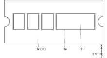
- 4 is a bottom view showing an example of a bottom structure of a sealing material included in the semiconductor device according to the first embodiment
- FIG. 11 is a bottom view showing another example of the bottom structure of the sealing material included in the semiconductor device according to the first embodiment.
- FIG. 11 is a bottom view showing still another example of the bottom structure of the sealing material included in the semiconductor device according to the first embodiment.
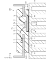
- FIG. 11 is a cross-sectional view showing an example of a structure around a die pad and a heat sink provided in a semiconductor device according to a second embodiment.
- FIG. 11 is a cross-sectional view showing another example of the peripheral structure of the die pad and the heat sink included in the semiconductor device according to the second embodiment.
- FIG. 11 is a cross-sectional view showing a state in which a semiconductor device according to a second embodiment is connected to a heat dissipation fin.
- 11 is a cross-sectional view showing an example of a die pad and its surrounding structure included in a semiconductor device according to a third embodiment.
- FIG. 11 is a bottom view showing still another example of the bottom structure of the sealing material included in the semiconductor device according to the first embodiment.
- FIG. 11 is a cross-sectional view showing an example of a structure around a die pad and a heat sink
- FIG. 13 is a cross-sectional view showing another example of the structure of the die pad and its periphery included in the semiconductor device according to the third embodiment.
- FIG. 13 is a block diagram showing a configuration of a power conversion system to which a power conversion device according to a fourth embodiment is applied.
- Fig. 1 is a top view of a semiconductor device 202 according to the first embodiment.
- Fig. 2 is a cross-sectional view taken along line AA in Fig. 1.
- the X direction, Y direction, and Z direction are mutually orthogonal.
- the X direction, Y direction, and Z direction shown in the following figures are also mutually orthogonal.
- the direction including the X direction and the -X direction, which is the opposite direction of the X direction is also referred to as the "X-axis direction”.
- the direction including the Y direction and the -Y direction, which is the opposite direction of the Y direction is also referred to as the "Y-axis direction”.
- the direction including the Z direction and the -Z direction, which is the opposite direction of the Z direction is also referred to as the "Z-axis direction”.
- the semiconductor device 202 includes a lead frame 2, a semiconductor element 3p, a control semiconductor element 3i, an insulating layer 9, and a sealing material 11.
- the lead frame 2 includes a die pad 2a, a power lead 2c (first lead), a control lead 2b (second lead), and a suspension lead 2n.
- the die pad 2a is formed in a plate shape. When viewed from the Z direction, the die pad 2a is formed in a rectangular shape.
- the die pad 2a has one side, 2s, and the other side, 2r.
- the side 2r is the side of the die pad 2a opposite to the side 2s.
- the sides 2s and 2r are flat surfaces.
- the die pad 2a is connected to one end of the power lead 2c via a suspension lead 2n.
- the control lead 2b is arranged on the opposite side of the die pad 2a to the power lead 2c. Specifically, the power lead 2c is arranged in the X direction relative to the die pad 2a, and the control lead 2b is arranged in the -X direction relative to the die pad 2a.
- the semiconductor element 3p is, for example, a power semiconductor element that operates at a high voltage. Note that the semiconductor element 3p is not limited to a power semiconductor element, and may be, for example, a semiconductor element that operates at a low voltage.
- a semiconductor element 3p is mounted on the surface 2s of the die pad 2a. Specifically, the semiconductor element 3p is bonded to the surface 2s of the die pad 2a by a bonding material 4.
- the bonding material 4 is, for example, solder.
- a control semiconductor element 3i is bonded to the surface in the Z direction at one end side of the control lead 2b by a bonding material 8.
- the bonding material 8 is, for example, solder.
- the wires 7s are connected to the control semiconductor element 3i.
- the wires 7s are signal transmission wires.
- the semiconductor element 3p and the control semiconductor element 3i are electrically connected by a wire 7s.
- the control semiconductor element 3i and the control lead 2b are electrically connected by a wire 7s.
- the semiconductor element 3p is electrically connected to the power lead 2c by a wire 7p.
- the surface 2r of the die pad 2a is provided with an insulating layer 9 having a very thin thickness.
- the insulating layer 9 is formed by coating the surface 2r of the die pad 2a with an insulating resin very thinly, at about 1 ⁇ m. In other words, the insulating layer 9 is disposed on the surface 2r of the die pad 2a.
- the insulating layer 9e is formed by thickly coating only the edge portion of the surface 2r of the die pad 2a with the insulating resin. In other words, the insulating layer 9e is a portion of the insulating layer 9 formed on the edge portion of the surface 2r of the die pad 2a.
- the thickness of the insulating layer 9e is formed to be thicker than the thickness of the portion of the insulating layer 9 other than the insulating layer 9e.
- the insulating layer 9e may be formed including the side surface of the die pad 2a. That is, as shown in FIG. 2, the insulating layer 9 is formed from the surface 2r of the die pad 2a to the side surface, and the insulating layer 9e may be formed from the edge portion of the surface 2r of the die pad 2a to the side surface.
- the side surface of the die pad 2a is the surface that connects the surface 2s and the surface 2r of the die pad 2a, in other words, the surface in the X-axis direction and the Y-axis direction of the die pad 2a.
- the sealing material 11 is, for example, a molded resin.
- the sealing material 11 seals the semiconductor element 3p, the control semiconductor element 3i, the wires 7p, 7s, the die pad 2a, the suspension lead 2n, the power lead 2c, the control lead 2b, and the insulating layer 9, while exposing the tip (other end) of the control lead 2b and the tip (other end) of the power lead 2c, and the portion of the insulating layer 9 formed on the surface 2r of the die pad 2a.
- the sealing material 11 is formed in a rectangular shape when viewed from the surface 2r side of the die pad 2a.
- the sealing material 11 has a surface 11s and a surface 11r.
- Surface 11s is the surface of the sealing material 11 in the Z direction.
- Surface 11r is the surface of the sealing material 11 opposite surface 11s and is the surface in the -Z direction.
- the control lead 2b protrudes in the -X direction from the -X side of the sealing material 11.
- the control lead 2b is bent so that the tip of the control lead 2b that is outside the sealing material 11 is parallel to the Z direction.
- the control lead 2b may be bent again so that it is parallel to the X direction.
- the power lead 2c protrudes in the X direction from the side of the sealing material 11 in the X direction.
- the control lead 2b is bent so that the tip of the control lead 2b that is outside the sealing material 11 is parallel to the Z direction. Furthermore, the control lead 2b may be bent again so that it is parallel to the X direction.
- each part will be specifically described.
- copper (Cu) or aluminum (Al) is used as the material for the lead frame 2.
- an alloy composed of copper (Cu) and aluminum (Al) may be used as the material for the lead frame 2.
- the surface of the lead frame 2 may be plated with nickel (Ni), silver (Ag), or gold (Au) to prevent oxidation. That is, a nickel plating film, a silver plating film, or a gold plating film may be formed on the surface of the lead frame 2. The plating film may be formed partially on the lead frame 2.
- the area on which the plating film is formed is also referred to as the "area to be plated.”
- the area to be plated is an area that is susceptible to surface oxidation.
- the area to be plated is, for example, the periphery of the area on the surface 2s of the die pad 2a where the semiconductor element 3p is bonded by the bonding material 4.
- the area to be plated is, for example, the periphery of the area on the Z-direction surface of the control lead 2b where the control semiconductor element 3i is bonded by the bonding material 8.
- the area to be plated is, for example, the area of the Z-direction surface of the control lead 2b around the area to which the wire 7s is connected.
- the area to be plated is, for example, the area of the Z-direction surface of the power lead 2c around the area to which the wire 7p is connected.
- the semiconductor element 3p is an element that functions, for example, as a switching element or a rectifying element.
- the switching element is, for example, an IGBT (Insulated Gate Bipolar Transistor) or a MOSFET (Metal-Oxide-Semiconductor Field-Effect Transistor).
- the rectifying element is a diode element.
- the material constituting the semiconductor element 3p is, for example, silicon (Si).
- the material constituting the semiconductor element 3p is not limited to silicon, and may be, for example, a wide bandgap semiconductor material such as silicon carbide (SiC), gallium nitride (GaN), or diamond (C).
- a wide bandgap semiconductor material is a material that has a bandgap wider than that of silicon.
- the semiconductor element 3p made of a wide bandgap semiconductor material is capable of operating using a large current and in a high-temperature environment. For this reason, it is preferable that the material constituting the semiconductor element 3p is a wide bandgap semiconductor material.
- a semiconductor device 202 equipped with such electronic components is known as an IPM (Intelligent Power Module).
- the material constituting the wires 7p and 7s may be aluminum (Al), copper (Cu), gold (Au), silver (Ag), or the like.
- the material constituting the wires 7p and 7s may also be an alloy.
- An alloy is composed of two or more metals selected from the metals aluminum (Al), copper (Cu), gold (Au), and silver (Ag).
- the material constituting the wires 7p and 7s may also be an alloy to which a metal element such as nickel (Ni) or iron (Fe) has been added.
- the shape of the wires 7p and 7s is, for example, a thin wire or a cylindrical shape.
- the cross-sectional shape of the wires 7p and 7s is, for example, a circle.
- the diameter of the circle is, for example, 10 ⁇ m or more and 500 ⁇ m or less.
- Wires 7p and 7s are bonded in a wire bonding process by existing methods such as ball bonding or wedge bonding. If the material constituting wire 7p is the same as the material constituting wire 7s, wires 7p and 7s can be bonded in the same wire bonding process.
- wire 7p is the main wiring. Therefore, the thickness of wire 7p is thicker than wire 7s. Note that the thickness of wire 7p may be the same as that of wire 7i. Also, the thickness of wire 7p may be thinner than that of wire 7s.
- the thickness of the wire 7p is the same as the thickness of the wire 7s.
- a semiconductor element having a complex configuration such as an IC (Integrated Circuit) or an LSI (Large Scale Integration) is mounted within the semiconductor device 202, the thickness of the wire 7p may be the same as the thickness of the wire 7s.
- the sealing material 11 may also be a composite material.
- the composite material is a material that contains, for example, a filler or other filler and a resin as main components.
- the filler is used to adjust the thermal expansion coefficient or mechanical properties of the sealing material 11.
- the resin contained in the composite material is, for example, a thermosetting resin with high electrical resistivity, such as an epoxy resin. It is preferable that the sealing material 11 has high insulation properties, good moldability, and reliability.
- the sealing material 11 is formed, for example, by a transfer molding method.
- the sealing material 11 seals a part of the lead frame 2 so that the tip (other end) of the power lead 2c and the tip (other end) of the control lead 2b are exposed from the sealing material 11.
- the sealing material 11 also seals the semiconductor element 3p, the control semiconductor element 3i, the wires 7p, 7s, the die pad 2a, the suspension lead 2n, the power lead 2c, the control lead 2b, and the insulating layer 9.
- the tip of the power lead 2c and the tip of the control lead 2b exposed from the sealing material 11 are electrically connected to a circuit board and other devices, not shown.
- the material constituting the insulating layer 9 is a highly insulating material, such as an epoxy resin, a fluorine resin, or a silicone resin.
- the thickness of the insulating layer 9 is about 1 ⁇ m or more, and is set taking into consideration the insulating properties required for the semiconductor device 202. However, if the thickness exceeds a certain level, the heat dissipation may be equal to or less than that of a so-called ceramic substrate in which ceramic is sandwiched between copper (Cu) plates, so it is preferable that the insulating layer 9 is about 30 ⁇ m or less in thickness.
- materials constituting ceramic substrates are alumina, aluminum nitride, silicon nitride, etc., and the thickness of the ceramic substrate is 250 ⁇ m or more. Therefore, if the thickness of the insulating layer 9 is less than that, heat dissipation greater than that of a ceramic substrate can be expected while maintaining insulation properties.
- Fig. 3 is a cross-sectional view showing the state in which the semiconductor device 202 according to the first embodiment is connected to the heat dissipation fins 22.
- Fig. 4 is a side view showing the state in which the semiconductor device 202 according to the first embodiment is connected to the heat dissipation fins 22 and arranged vertically.
- the sealing material 11 of the semiconductor device 202 is connected to the heat dissipation fins 22 via the grease 23.
- the insulating layer 9e arranged on the edge portion of the surface 2r of the die pad 2a protrudes in the -Z direction from the portion of the insulating layer 9 surrounded by the insulating layer 9e.
- the portion of the insulating layer 9 surrounded by the insulating layer 9e is recessed in the Z direction from the insulating layer 9e. Since the grease 23 can be held in the recessed portion formed on the surface 2r side of the die pad 2a, the thickness of the grease 23 present directly below the die pad 2a can be kept thin and constant.
- the insulating layer 9e arranged on the edge portion protrudes from the surface of the sealing material 11.
- the grease 23 may be present between the protruding insulating layer 9e and the heat dissipation fins 22, or the insulating layer 9e and the heat dissipation fins 22 may be in direct contact with each other.
- the grease 23 is applied thicker than necessary to absorb variations in the warping of the semiconductor device 202 or the heat dissipation fins 22.
- a thicker thermally conductive sheet may be used instead of the grease 23. In either case, the presence of an excessively thick grease 23 or thermally conductive sheet directly below the die pad 2a contributes to the deterioration of thermal resistance.
- the semiconductor device 202 may be used in a machine or device that generates vibrations. Also, as shown in FIG. 4, the semiconductor device 202 and heat dissipation fins 22 may be installed vertically. In such a case, if the grease 23 wets and spreads to the outside due to vibration, a gap is created between the sealing material 11 and the heat dissipation fins 22. Due to this gap, heat generated from the semiconductor element 3p cannot be efficiently transferred to the heat dissipation fins 22, and the heat dissipation performance of the semiconductor device 202 may be reduced.
- the insulating layer 9e surrounds the surface 2r of the die pad 2a, thereby preventing the grease 23 from leaking and spreading outside the edge of the surface 2r of the die pad 2a.
- This allows the grease 23 to be held directly below the die pad 2a on which the semiconductor element 3p, which is the heat source, is mounted, making it possible to maintain constant heat dissipation in the semiconductor device 202.
- directly below the die pad 2a refers to the -Z direction of the die pad 2a in FIG. 3, and refers to the X direction of the die pad (not shown) in FIG. 4.
- the semiconductor device 202 has high heat dissipation performance because the semiconductor element 3p is connected to the heat dissipation fins 22 via the shortest possible distance without the low thermal conductivity sealing material 11 in the heat dissipation path from the semiconductor element 3p.
- the semiconductor element 3p is connected to the heat dissipation fins 22 via the shortest possible distance without the low thermal conductivity sealing material 11 in the heat dissipation path from the semiconductor element 3p.
- a short circuit occurs when the semiconductor element 3p is energized because the sealing material 11 that provided insulation between the semiconductor element 3p and the heat dissipation fins 22 is no longer present.
- the insulating layer 9 is formed by coating the surface 2r of the die pad 2a with an insulating resin in a very thin layer of about 1 ⁇ m, which allows for both insulation and high heat dissipation.
- the sealing material 11 and the heat dissipation fins 22 are connected using a screw fastening method. Although not shown, the sealing material 11 and the heat dissipation fins 22 are fastened to each other by inserting a screw (not shown) through a screw hole 12 (see FIG. 1) extending in the vertical direction provided on the side of the sealing material 11.
- FIG. 5 is a bottom view showing an example of the bottom structure of the sealing material 11 provided in the semiconductor device 202 according to the first embodiment.
- FIG. 6 is a bottom view showing another example of the bottom structure of the sealing material 11 provided in the semiconductor device 202 according to the first embodiment.
- FIG. 7 is a bottom view showing yet another example of the bottom structure of the sealing material 11 provided in the semiconductor device 202 according to the first embodiment.
- the lead frame 2 includes a plurality of die pads 2a, which are spaced apart from one another along the longitudinal direction (Y-axis direction) of the encapsulant 11.
- an insulating layer 9e having a thickness greater than the insulating layer 9 is formed so as to surround the surface 2r of the die pad 2a.
- the width of the insulating layer 9e is uniform.
- the thickness of the grease 23 applied when attaching the heat dissipation fins 22 can be adjusted depending on the difference in thickness between the insulating layer 9e and the other parts of the insulating layer 9, so the thickness of the insulating layer 9e can be determined according to the warping and surface irregularities of the semiconductor device 202 or the heat dissipation fins 22.
- the adhesion between resin and metal is weaker than the adhesion between resin and resin. Therefore, when the semiconductor device 202 is in operation, i.e., when the semiconductor element 3p is generating heat, the edge portion of the surface 2r of the die pad 2a where the most stress occurs often becomes the starting point for peeling between the sealing material 11 and the die pad 2a.
- the insulating layer 9 including the insulating layer 9e is formed from the face 2r to the side of the die pad 2a, so that the sealing material 11 and the insulating layer 9e are in close contact even at the edge of the face 2r of the die pad 2a where the most stress occurs.
- the insulating layer 9e adheres more firmly to the sealing material 11 than the metal material of the die pad 2a, so peeling of the sealing material 11 can be suppressed. As a result, high reliability can be ensured in the semiconductor device 202.
- the width of the insulating layer 9e formed on a specific side at the edge portion of the surface 2r of the die pad 2a may be made wider than the width of the insulating layer 9e formed on the other sides.
- Smile warping or cry warping occurs in the semiconductor device 202 mainly due to the difference in thermal expansion coefficient between the sealing material 11 and the lead frame 2, and the difference in thermal expansion coefficient between other components.
- the semiconductor device 202 and the heat dissipation fin 22 are screwed together, the above-mentioned warping is corrected, so that the largest stress is applied to the side of the die pad 2a closest to the screw hole 12. Therefore, as shown in FIG. 6, the width of the insulating layer 9e is widened by adding multiple coatings to the side of the die pad 2a closest to the screw hole 12, which is subjected to the most stress when the screws are tightened.
- the width of the part of the insulating layer 9e adjacent to the rectangular short side (side extending in the X-axis direction) of the sealing material 11 is formed wider than the width of the other parts of the insulating layer 9e. This makes it possible to take measures against stress when the screws are tightened.
- the edge portion of the surface 2r of the die pad 2a, where the most stress occurs often becomes the starting point for peeling between the sealing material 11 and the die pad 2a. As shown in FIG. 2, stress is most likely to concentrate in the bent portion, which is the connection portion between the die pad 2a and the suspension lead 2n, and peeling is likely to occur from there.
- the width of the insulating layer 9e is increased by applying multiple coatings to the side of the die pad 2a, which is subject to the most stress when heat is generated. More specifically, the width of the portion of the insulating layer 9e adjacent to the long side (the side extending in the Y-axis direction) of the rectangular shape of the sealing material 11 is made wider than the width of the other portions of the insulating layer 9e. This makes it possible to deal with stress when heat is generated.
- the material that constitutes the heat dissipation fins 22 is, for example, an alloy.
- the alloy is, for example, aluminum (Al) to which at least one of the metals magnesium (Mg) and manganese (Mn) has been added.
- the material constituting the heat dissipation fins 22 is not limited to an alloy, and may be a metal other than an alloy.
- the material constituting the heat dissipation fins 22 may be, for example, copper (Cu).
- the heat dissipation fins 22 may also be a plate made of aluminum (Al).
- the material constituting the heat dissipation fins 22 may be a material other than metal.
- the material constituting the heat dissipation fins 22 may be, for example, an inorganic or organic material with high thermal conductivity.
- the semiconductor device 202 includes the lead frame 2 including the die pad 2a, the power lead 2c having one end connected to the die pad 2a, and the control lead 2b arranged on the opposite side of the power lead 2c with respect to the die pad 2a, the semiconductor element 3p mounted on the surface 2s of the die pad 2a, the control semiconductor element 3i mounted on one surface of one end of the control lead 2b and controlling the semiconductor element 3p, the insulating layer 9 arranged from the surface 2r of the die pad 2a opposite to the surface 2s to the side connecting the surface 2r and the surface 2s, and the sealing material 11 that seals the semiconductor element 3p, the control semiconductor element 3i, and the lead frame 2 with the portion of the insulating layer 9 arranged on the surface 2r of the die pad 2a exposed.
- the thickness of the insulating layer 9e which is a portion of the insulating layer 9 arranged on the edge portion of the surface 2r of the die pad 2a, is thicker than the thickness of the other portions, and the insulating layer 9e protrudes from the surface of the sealing material 11.
- the lead frame 2 also includes multiple die pads 2a, the sealing material 11 is formed in a rectangular shape when viewed from the surface 2r side of the multiple die pads 2a, the multiple die pads 2a are arranged at intervals along the longitudinal direction (Y-axis direction) of the sealing material 11, and the width of the insulating layer 9e is uniform.
- the grease 23 is placed on the surface 2r side of the die pad 2a, but the thick insulating layer 9e placed on the edge portion of the surface 2r of the die pad 2a surrounds the surface 2r of the die pad 2a, thereby preventing the grease 23 from spreading outward to the outside of the edge portion of the surface 2r of the die pad 2a.
- the insulating layer 9e arranged on the edge portion of the surface 2r of the die pad 2a adheres more firmly to the sealing material 11 than the metal material of the die pad 2a, so peeling of the sealing material 11 can be suppressed. As a result, the reliability of the semiconductor device 202 can be improved.
- the thickness of the insulating layer 9 is 1 ⁇ m or more and 30 ⁇ m or less, so it does not significantly impede heat dissipation in the semiconductor device 202.
- the width of the portion of the insulating layer 9e adjacent to the short side (the side extending in the X-axis direction) of the rectangular shape of the sealing material 11 is made wider than the width of the other portions of the insulating layer 9e. This makes it possible to deal with stress when tightening the screws.
- the width of the portion of the insulating layer 9e adjacent to the long side (the side extending in the Y-axis direction) of the rectangular shape of the sealing material 11 is made wider than the width of the other portions of the insulating layer 9e. This makes it possible to deal with stress caused by heat generation.
- Fig. 8 is a cross-sectional view showing an example of the structure around the die pad 2a and the heat sink 10 of the semiconductor device 202 according to the second embodiment.
- Fig. 9 is a cross-sectional view showing another example of the structure around the die pad 2a and the heat sink 10 of the semiconductor device 202 according to the second embodiment.
- Fig. 10 is a cross-sectional view showing a state in which the semiconductor device 202 according to the second embodiment and the heat dissipation fin 22 are connected.
- the same components as those described in the first embodiment are denoted by the same reference numerals, and the description thereof will be omitted.
- the semiconductor device 202 further includes a heat sink 10, and the location where the insulating layer 9 is disposed is different from that in the first embodiment. Note that the sealing material 11 is not shown in FIG. 8.
- the heat sink 10 is disposed on the surface 2r of the die pad 2a.
- the heat sink 10 has a surface 10s (one surface) that faces the surface 2r of the die pad 2a, a surface 10r (the other surface) opposite the surface 10s, and a side surface that connects the surface 10s and the surface 10r.
- the side surfaces of the heat sink 10 are the surfaces in the X-axis direction and the Y-axis direction of the heat sink 10.
- the insulating layer 9 is disposed from the face 10s of the heat sink 10 to the side.
- An insulating layer 9e is also formed on the edge of the face 10s of the heat sink 10.
- the insulating layer 9e is a portion of the insulating layer 9 formed on the edge of the face 10s of the heat sink 10.
- the insulating layer 9e may also be formed on the side of the heat sink 10. That is, as shown in FIG. 8, the insulating layer 9 is formed from the face 10s of the heat sink 10 to the side, and the insulating layer 9e may be formed from the edge of the face 10s of the heat sink 10 to the side.
- the heat sink 10 on which the insulating layer 9 including the insulating layer 9e is disposed and the die pad 2a are bonded by thermocompression bonding of the sealing material 11 (see FIG. 2) during transfer molding, and are mold-sealed together with other components.
- the sealing material 11 (see FIG. 2) seals the semiconductor element 3p, the control semiconductor element 3i (see FIG. 2), the lead frame 2, and the heat sink 10, with the surface 10r of the heat sink 10 exposed.
- the reliability of the semiconductor device 202 can be improved while improving the heat dissipation.
- the heat sink 10 on which the insulating layer 9 including the insulating layer 9e is arranged inside the semiconductor device 202 the heat concentrated directly below the semiconductor element 3p can be spread by the heat sink 10.
- the heat dissipation fins 22 see FIG. 3
- the insulating layer 9e has the same thickness as in the first embodiment, it does not significantly impede heat dissipation in the semiconductor device 202.
- the thickness of the insulating layer 9 including the insulating layer 9e is about 1 ⁇ m or more and about 30 ⁇ m or less.
- the rigidity of the lead frame 2, which has a smaller thermal expansion coefficient than the sealing material 11, can be improved, which also helps to suppress warping of the semiconductor device 202.
- the insulating layer 9 is formed from the surface 10r of the heat sink 10 to the side, and the insulating layer 9e may be formed from the edge portion of the surface 10r of the heat sink 10 to the side.
- the sealant 11 is omitted in FIG. 9.
- the sealant 11 (see FIG. 2) seals the semiconductor element 3p, the control semiconductor element 3i (see FIG. 2), the lead frame 2, and the heat sink 10 while exposing the portion of the insulating layer 9 arranged on the surface 10r of the heat sink 10.
- the die pad 2a and the heat sink 10 are in close contact without the insulating layer 9, and the heat of the semiconductor element 3p can be spread to the heat sink 10 more efficiently than in the structure of FIG. 8.
- the sealing material 11 is connected to the heat dissipation fins 22 via grease 23.
- the thickness of the grease 23 directly below the die pad 2a can be kept thin and constant at the bottom of the recess formed by the insulating layer 9 arranged on the surface 2r of the die pad 2a and the insulating layer 9e arranged on the edge portion.
- Fig. 11 is a cross-sectional view showing an example of the structure of the die pad 2a and its periphery provided in the semiconductor device 202 according to the third embodiment.
- Fig. 12 is a cross-sectional view showing another example of the structure of the die pad 2a and its periphery provided in the semiconductor device 202 according to the third embodiment. Note that in the third embodiment, the same components as those described in the first and second embodiments are denoted by the same reference numerals, and description thereof will be omitted.
- the side surface of the die pad 2a is roughened, and then an insulating layer 9s is formed by a conventional method, thereby achieving the same anchor effect as in FIG. 11. Because coating can be performed by a conventional method, it is easy to form an insulating layer 9s with a rough surface, and the reliability of the semiconductor device 202 can be improved at low cost.
- the roughened insulating layer 9s may be made thicker on certain sides.
- the semiconductor device 202 according to the above-mentioned first to third embodiments is applied to a power conversion device 200.
- the application of the semiconductor device 202 according to the first to third embodiments is not limited to a specific power conversion device, hereinafter, as a fourth embodiment, a case where the semiconductor device 202 according to the first to third embodiments is applied to a three-phase inverter will be described.
- FIG. 13 is a block diagram showing the configuration of a power conversion system that uses a power conversion device 200 according to embodiment 4.
- the power conversion system shown in FIG. 13 is composed of a power source 100, a power conversion device 200, and a load 300.
- the power source 100 is a DC power source and supplies DC power to the power conversion device 200.
- the power source 100 can be composed of various things, for example, a DC system, a solar cell, or a storage battery, or it may be composed of a rectifier circuit connected to an AC system or an AC/DC converter.
- the power source 100 may also be composed of a DC/DC converter that converts the DC power output from the DC system into a specified power.
- the power conversion device 200 is a three-phase inverter connected between the power source 100 and the load 300, converts the DC power supplied from the power source 100 into AC power, and supplies the AC power to the load 300. As shown in FIG. 13, the power conversion device 200 includes a main conversion circuit 201 that converts the DC power into AC power and outputs it, and a control circuit 203 that outputs a control signal to the main conversion circuit 201 to control the main conversion circuit 201.
- the load 300 is a three-phase motor that is driven by AC power supplied from the power conversion device 200.
- the load 300 is not limited to a specific use, but is a motor mounted on various electrical devices, and is used, for example, as a motor for hybrid cars, electric cars, railroad cars, elevators, or air conditioning equipment.
- the power conversion device 200 will be described in detail below.
- the main conversion circuit 201 includes a switching element (not shown) and a freewheeling diode (not shown), and converts the DC power supplied from the power source 100 into AC power by switching the switching element, and supplies it to the load 300.
- the main conversion circuit 201 in this embodiment is a two-level three-phase full bridge circuit, and can be configured from six switching elements and six freewheeling diodes connected in inverse parallel to each switching element.
- At least one of the switching elements and free wheel diodes of the main conversion circuit 201 is configured with a semiconductor device 202 corresponding to any one of the above-mentioned embodiments 1 to 3.
- the main conversion circuit 201 is equipped with the semiconductor device 202 according to embodiment 1.
- the six switching elements are connected in series in pairs to configure upper and lower arms, and each upper and lower arm configures each phase (U phase, V phase, W phase) of the full bridge circuit.
- the output terminals of each upper and lower arm i.e., the three output terminals of the main conversion circuit 201, are connected to the load 300.
- the main conversion circuit 201 also includes a drive circuit (not shown) for driving each switching element, but the drive circuit may be built into the semiconductor device 202, or may be configured to include a drive circuit separate from the semiconductor device 202.
- the drive circuit generates drive signals for driving the switching elements of the main conversion circuit 201 and supplies them to the control electrodes of the switching elements of the main conversion circuit 201. Specifically, in accordance with a control signal from the control circuit 203 (described later), a drive signal for turning the switching element on and a drive signal for turning the switching element off are output to the control electrodes of each switching element.
- the drive signal When maintaining a switching element in the on state, the drive signal is a voltage signal (on signal) equal to or higher than the threshold voltage of the switching element, and when maintaining a switching element in the off state, the drive signal is a voltage signal (off signal) equal to or lower than the threshold voltage of the switching element.
- the control circuit 203 controls the switching elements of the main conversion circuit 201 so that the desired power is supplied to the load 300. Specifically, it calculates the time (on time) that each switching element of the main conversion circuit 201 should be in the on state based on the power to be supplied to the load 300.
- the main conversion circuit 201 can be controlled by PWM control, which modulates the on time of the switching elements according to the voltage to be output. Then, it outputs a control command (control signal) to a drive circuit provided in the main conversion circuit 201 so that an on signal is output to the switching element that should be in the on state at each point in time, and an off signal is output to the switching element that should be in the off state.
- the drive circuit outputs an on signal or an off signal as a drive signal to the control electrode of each switching element according to this control signal.
- the semiconductor device 202 is used as the switching element and freewheel diode of the main conversion circuit 201, thereby improving reliability.
- the semiconductor device 202 according to the first to third embodiments is applied to a two-level three-phase inverter, but the application of the semiconductor device 202 according to the first to third embodiments is not limited to this, and the semiconductor device 202 can be applied to various power conversion devices.
- a two-level power conversion device is used, but a three-level or multi-level power conversion device may also be used, and when supplying power to a single-phase load, the semiconductor device 202 according to the first to third embodiments may be applied to a single-phase inverter.
- the semiconductor device 202 according to the first to third embodiments can also be applied to a DC/DC converter or an AC/DC converter.
- the power conversion device 200 to which the semiconductor device 202 according to the first to third embodiments is applied is not limited to the case where the load described above is an electric motor, but can also be used, for example, as a power supply device for an electric discharge machine, a laser processing machine, an induction heating cooker, or a non-contact power supply system, and can also be used as a power conditioner for a solar power generation system, a power storage system, etc.
- each embodiment can be freely combined, modified, or omitted as appropriate.
- a lead frame including a die pad, a first lead having one end connected to the die pad, and a second lead disposed on an opposite side of the die pad from the first lead; a semiconductor element mounted on one surface of the die pad; a control semiconductor element mounted on one surface of one end of the second lead and controlling the semiconductor element; an insulating layer disposed from a second surface of the die pad opposite to the first surface to a side surface connecting the first surface and the second surface; a sealing material that seals the semiconductor element, the control semiconductor element, and the lead frame in a state in which a portion of the insulating layer that is disposed on the other surface of the die pad is exposed, a thickness of the insulating layer at a portion disposed on an edge portion of the other surface of the die pad is greater than a thickness of the other portion; A semiconductor device, wherein a portion of the insulating layer disposed at the edge portion protrudes from a surface of the sealing material.
- the lead frame includes a plurality of the die pads, the sealing material is formed in a rectangular shape when viewed from the other surface side of the plurality of die pads, The die pads are spaced apart from one another along a longitudinal direction of the encapsulant, 3.
- the lead frame includes a plurality of the die pads, the sealing material is formed in a rectangular shape when viewed from the other surface side of the plurality of die pads, The die pads are spaced apart from one another along a longitudinal direction of the encapsulant, 3.
- a width of the insulating layer at the edge portion adjacent to the short side of the rectangular shape of the sealing material is wider than a width of the other portion at the edge portion.
- the lead frame includes a plurality of the die pads, the sealing material is formed in a rectangular shape when viewed from the other surface side of the plurality of die pads, The die pads are spaced apart from one another along a longitudinal direction of the encapsulant, 3.
- a width of the insulating layer at the edge portion adjacent to the long side of the rectangular shape of the sealing material is wider than a width of the other portion at the edge portion.
- a lead frame including a die pad, a first lead having one end connected to the die pad, and a second lead disposed on an opposite side of the die pad from the first lead; a semiconductor element mounted on one surface of the die pad; a control semiconductor element mounted on one surface of one end of the second lead and controlling the semiconductor element; a heat sink disposed on the other surface of the die pad opposite to the one surface, the heat sink having one surface facing the other surface of the die pad, the other surface opposite to the one surface, and a side surface connecting the one surface and the other surface; an insulating layer disposed across the other surface of the heat sink to the side surface; a sealing material that seals the semiconductor element, the control semiconductor element, the lead frame, and the heat sink in a state in which a portion of the insulating layer that is disposed on the other surface of the heat sink is exposed, a thickness of the insulating layer at a portion disposed on the edge portion of the other surface of the heat sink is greater than a thickness of the other portion of the
- (Appendix 8) 8. The semiconductor device according to claim 6, wherein the insulating layer has a surface having an arithmetic mean roughness Ra of 0.05 ⁇ m or more and 0.1 mm or less, the surface being disposed on the edge portion of the other side of the heat sink.
- a power conversion device comprising:
Landscapes
- Cooling Or The Like Of Semiconductors Or Solid State Devices (AREA)
Priority Applications (1)
| Application Number | Priority Date | Filing Date | Title |
|---|---|---|---|
| JP2025559097A JPWO2025109919A1 (https=) | 2023-11-21 | 2024-10-17 |
Applications Claiming Priority (2)
| Application Number | Priority Date | Filing Date | Title |
|---|---|---|---|
| JP2023-197160 | 2023-11-21 | ||
| JP2023197160 | 2023-11-21 |
Publications (1)
| Publication Number | Publication Date |
|---|---|
| WO2025109919A1 true WO2025109919A1 (ja) | 2025-05-30 |
Family
ID=95826515
Family Applications (1)
| Application Number | Title | Priority Date | Filing Date |
|---|---|---|---|
| PCT/JP2024/036978 Pending WO2025109919A1 (ja) | 2023-11-21 | 2024-10-17 | 半導体装置および電力変換装置 |
Country Status (2)
| Country | Link |
|---|---|
| JP (1) | JPWO2025109919A1 (https=) |
| WO (1) | WO2025109919A1 (https=) |
Citations (5)
| Publication number | Priority date | Publication date | Assignee | Title |
|---|---|---|---|---|
| JP2002110867A (ja) * | 2000-10-02 | 2002-04-12 | Toshiba Corp | 半導体装置及びその製造方法 |
| JP2008153430A (ja) * | 2006-12-18 | 2008-07-03 | Mitsubishi Electric Corp | 放熱基板並びに熱伝導性シートおよびこれらを用いたパワーモジュール |
| JP2011114010A (ja) * | 2009-11-24 | 2011-06-09 | Fuji Electric Holdings Co Ltd | 半導体モジュールおよびその製造方法ならびに電気機器 |
| JP2015023212A (ja) * | 2013-07-22 | 2015-02-02 | ローム株式会社 | パワーモジュールおよびその製造方法 |
| WO2019235267A1 (ja) * | 2018-06-04 | 2019-12-12 | ローム株式会社 | 半導体装置 |
-
2024
- 2024-10-17 WO PCT/JP2024/036978 patent/WO2025109919A1/ja active Pending
- 2024-10-17 JP JP2025559097A patent/JPWO2025109919A1/ja active Pending
Patent Citations (5)
| Publication number | Priority date | Publication date | Assignee | Title |
|---|---|---|---|---|
| JP2002110867A (ja) * | 2000-10-02 | 2002-04-12 | Toshiba Corp | 半導体装置及びその製造方法 |
| JP2008153430A (ja) * | 2006-12-18 | 2008-07-03 | Mitsubishi Electric Corp | 放熱基板並びに熱伝導性シートおよびこれらを用いたパワーモジュール |
| JP2011114010A (ja) * | 2009-11-24 | 2011-06-09 | Fuji Electric Holdings Co Ltd | 半導体モジュールおよびその製造方法ならびに電気機器 |
| JP2015023212A (ja) * | 2013-07-22 | 2015-02-02 | ローム株式会社 | パワーモジュールおよびその製造方法 |
| WO2019235267A1 (ja) * | 2018-06-04 | 2019-12-12 | ローム株式会社 | 半導体装置 |
Also Published As
| Publication number | Publication date |
|---|---|
| JPWO2025109919A1 (https=) | 2025-05-30 |
Similar Documents
| Publication | Publication Date | Title |
|---|---|---|
| JP7196815B2 (ja) | 半導体モジュール及び電力変換装置 | |
| CN109727960B (zh) | 半导体模块、其制造方法以及电力变换装置 | |
| CN112864113B (zh) | 功率器件、功率器件组件与相关装置 | |
| JP7199167B2 (ja) | パワー半導体モジュール、電力変換装置、およびパワー半導体モジュールの製造方法 | |
| JP6752381B1 (ja) | 半導体モジュールおよび電力変換装置 | |
| JP6952889B2 (ja) | パワー半導体モジュール及びその製造方法並びに電力変換装置 | |
| JP6826665B2 (ja) | 半導体装置、半導体装置の製造方法及び電力変換装置 | |
| JP7561677B2 (ja) | 電力半導体装置、電力半導体装置の製造方法及び電力変換装置 | |
| CN113646876B (zh) | 功率半导体模块以及电力变换装置 | |
| CN111052325B (zh) | 半导体模块以及电力转换装置 | |
| WO2019235146A1 (ja) | 半導体モジュール | |
| WO2020148879A1 (ja) | 半導体装置、半導体装置の製造方法及び電力変換装置 | |
| US11997837B2 (en) | Power semiconductor module and power converter | |
| CN115023810B (zh) | 半导体装置以及电力变换装置 | |
| WO2025109919A1 (ja) | 半導体装置および電力変換装置 | |
| JP2024077117A (ja) | 半導体装置、半導体装置の製造方法および電力変換装置 | |
| WO2024204310A1 (ja) | 半導体装置、電力変換装置、インバータ基板、および放熱フィン | |
| JP7851410B2 (ja) | 半導体装置、電力変換装置および半導体装置の製造方法 | |
| JP7781340B2 (ja) | パワー半導体装置、パワーモジュール及び電力変換装置 | |
| JP7546783B2 (ja) | 半導体装置、電力変換装置、および、半導体装置の製造方法 | |
| JP7334369B1 (ja) | パワーモジュール及び電力変換装置 | |
| US20250069984A1 (en) | Power semiconductor device and power electronics assembly | |
| JPWO2020245998A1 (ja) | 半導体装置、電力変換装置および半導体装置の製造方法 | |
| JP2025167526A (ja) | 半導体装置、電力変換装置、及び半導体装置の製造方法 | |
| JP2024139935A (ja) | 半導体装置および電力変換装置 |
Legal Events
| Date | Code | Title | Description |
|---|---|---|---|
| 121 | Ep: the epo has been informed by wipo that ep was designated in this application |
Ref document number: 24893913 Country of ref document: EP Kind code of ref document: A1 |
|
| ENP | Entry into the national phase |
Ref document number: 2025559097 Country of ref document: JP Kind code of ref document: A |