WO2025100280A1 - プラズマ評価システム及びプラズマ評価方法 - Google Patents
プラズマ評価システム及びプラズマ評価方法 Download PDFInfo
- Publication number
- WO2025100280A1 WO2025100280A1 PCT/JP2024/038272 JP2024038272W WO2025100280A1 WO 2025100280 A1 WO2025100280 A1 WO 2025100280A1 JP 2024038272 W JP2024038272 W JP 2024038272W WO 2025100280 A1 WO2025100280 A1 WO 2025100280A1
- Authority
- WO
- WIPO (PCT)
- Prior art keywords
- plasma
- circuit
- equivalent circuit
- evaluation
- derivation
- Prior art date
- Legal status (The legal status is an assumption and is not a legal conclusion. Google has not performed a legal analysis and makes no representation as to the accuracy of the status listed.)
- Pending
Links
Images

Classifications
-
- H—ELECTRICITY
- H05—ELECTRIC TECHNIQUES NOT OTHERWISE PROVIDED FOR
- H05H—PLASMA TECHNIQUE; PRODUCTION OF ACCELERATED ELECTRICALLY-CHARGED PARTICLES OR OF NEUTRONS; PRODUCTION OR ACCELERATION OF NEUTRAL MOLECULAR OR ATOMIC BEAMS
- H05H1/00—Generating plasma; Handling plasma
-
- H—ELECTRICITY
- H05—ELECTRIC TECHNIQUES NOT OTHERWISE PROVIDED FOR
- H05H—PLASMA TECHNIQUE; PRODUCTION OF ACCELERATED ELECTRICALLY-CHARGED PARTICLES OR OF NEUTRONS; PRODUCTION OR ACCELERATION OF NEUTRAL MOLECULAR OR ATOMIC BEAMS
- H05H1/00—Generating plasma; Handling plasma
- H05H1/24—Generating plasma
- H05H1/46—Generating plasma using applied electromagnetic fields, e.g. high frequency or microwave energy
-
- H—ELECTRICITY
- H10—SEMICONDUCTOR DEVICES; ELECTRIC SOLID-STATE DEVICES NOT OTHERWISE PROVIDED FOR
- H10P—GENERIC PROCESSES OR APPARATUS FOR THE MANUFACTURE OR TREATMENT OF DEVICES COVERED BY CLASS H10
- H10P50/00—Etching of wafers, substrates or parts of devices
- H10P50/20—Dry etching; Plasma etching; Reactive-ion etching
- H10P50/24—Dry etching; Plasma etching; Reactive-ion etching of semiconductor materials
- H10P50/242—Dry etching; Plasma etching; Reactive-ion etching of semiconductor materials of Group IV materials
Definitions
- This disclosure relates to a plasma evaluation system and a plasma evaluation method.
- Patent Document 1 discloses that the load impedance seen from the wafer (focus ring) surface can be expressed as a parallel connection of the resistance component (R1) and capacitance component (C4) of the ion sheath on the wafer (focus ring) surface, and a parallel connection of the plasma impedance component (Zp) and the resistance component (R2) and capacitance component (C5) of the ion sheath on the ground surface, all connected in series.
- Patent Document 1 also discloses that the sheath resistance component can be expressed as a diode, and that plasma resistance, plasma capacitance, and plasma inductance can also be included.
- the present disclosure provides a plasma evaluation system and a plasma evaluation method that can calculate evaluation parameters that represent plasma characteristics.
- a plasma evaluation system includes a plasma processing device, a derivation circuit section that is connected to a high-frequency application line for generating plasma in the plasma processing device and derives an equivalent circuit of the generated plasma, and a simulator section that calculates evaluation parameters that represent the characteristics of the plasma by performing a simulation of the plasma based on the parameters of the equivalent circuit derived by the derivation circuit section.
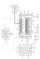
- FIG. 1 is a diagram illustrating an example of a plasma evaluation system according to an embodiment of the present disclosure.
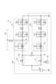
- FIG. 2 is a diagram showing an example of a bridge circuit constituting the derivation circuit unit in this embodiment.
- FIG. 3 is a diagram showing an example of the configuration of the derivation circuit unit in this embodiment.
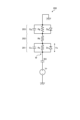
- FIG. 4 is a diagram showing an example of an equivalent circuit of plasma in this embodiment.
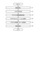
- FIG. 5 is a flowchart showing an example of the plasma evaluation process in this embodiment.
- a matcher positioner and a VI probe are used to measure the chamber impedance and Vpp, Vdc, etc., respectively.
- a Langmuir probe is used to measure the electron density of the plasma.
- an equivalent circuit analysis of plasma is used to optimize the focus ring structure.
- FIG. 1 is a diagram showing an example of a plasma evaluation system according to an embodiment of the present disclosure.
- the plasma evaluation system 1 includes a capacitively coupled plasma processing device 2, a control unit 3, a derivation circuit unit 50, and a waveform detector 60.
- the capacitively coupled plasma processing device 2 includes a plasma processing chamber 10, a gas supply unit 20, a power supply 30, and an exhaust system 40.
- the derivation circuit unit 50 and the waveform detector 60 may be included in the plasma processing device 2.
- the plasma processing device 2 also includes a substrate support unit 11 and a gas introduction unit.
- the gas introduction unit is configured to introduce at least one processing gas into the plasma processing chamber 10.
- the gas introduction unit includes a shower head 13.
- the substrate support unit 11 is disposed in the plasma processing chamber 10.
- the shower head 13 is disposed above the substrate support unit 11. In one embodiment, the shower head 13 constitutes at least a part of the ceiling of the plasma processing chamber 10.
- the plasma processing chamber 10 has a plasma processing space 10s defined by a showerhead 13, a sidewall 10a of the plasma processing chamber 10, and a substrate support 11.
- the plasma processing chamber 10 has at least one gas supply port for supplying at least one processing gas to the plasma processing space 10s, and at least one gas exhaust port for exhausting gas from the plasma processing space 10s.
- the plasma processing chamber 10 is grounded.
- the showerhead 13 and the substrate support 11 are electrically insulated from the housing of the plasma processing chamber 10.
- the substrate support 11 includes a main body 111 and a ring assembly 112.
- the main body 111 has a central region 111a for supporting the substrate W and an annular region 111b for supporting the ring assembly 112.
- a wafer is an example of a substrate W.
- the annular region 111b of the main body 111 surrounds the central region 111a of the main body 111 in a plan view.
- the substrate W is disposed on the central region 111a of the main body 111
- the ring assembly 112 is disposed on the annular region 111b of the main body 111 so as to surround the substrate W on the central region 111a of the main body 111. Therefore, the central region 111a is also called a substrate support surface for supporting the substrate W, and the annular region 111b is also called a ring support surface for supporting the ring assembly 112.
- the main body 111 includes a base 1110 and an electrostatic chuck 1111.
- the base 1110 includes a conductive member.
- the conductive member of the base 1110 may function as a lower electrode.
- the electrostatic chuck 1111 is disposed on the base 1110.
- the electrostatic chuck 1111 includes a ceramic member 1111a and an electrostatic electrode 1111b disposed within the ceramic member 1111a.
- the ceramic member 1111a has a central region 111a. In one embodiment, the ceramic member 1111a also has an annular region 111b. Note that other members surrounding the electrostatic chuck 1111, such as an annular electrostatic chuck or an annular insulating member, may be provided in the annular region 111b.
- the ring assembly 112 may be disposed on the annular electrostatic chuck or the annular insulating member, or may be disposed on both the electrostatic chuck 1111 and the annular insulating member.
- at least one RF/DC electrode coupled to an RF (Radio Frequency) power source 31 and/or a DC (Direct Current) power source 32 described later may be disposed within the ceramic member 1111a.
- the at least one RF/DC electrode functions as a lower electrode.
- the RF/DC electrode is also called a bias electrode.
- the conductive member of the base 1110 and the at least one RF/DC electrode may function as multiple lower electrodes.
- the electrostatic electrode 1111b may function as a lower electrode.
- the substrate support 11 includes at least one lower electrode.
- the ring assembly 112 includes one or more annular members.
- the one or more annular members include one or more edge rings and at least one cover ring.
- the edge rings are formed of a conductive or insulating material, and the cover rings are formed of an insulating material.
- the substrate support 11 may also include a temperature adjustment module configured to adjust at least one of the electrostatic chuck 1111, the ring assembly 112, and the substrate to a target temperature.
- the temperature adjustment module may include a heater, a heat transfer medium, a flow passage 1110a, or a combination thereof.
- a heat transfer fluid such as brine or a gas flows through the flow passage 1110a.
- the flow passage 1110a is formed in the base 1110, and one or more heaters are disposed in the ceramic member 1111a of the electrostatic chuck 1111.
- the substrate support 11 may also include a heat transfer gas supply configured to supply a heat transfer gas to a gap between the back surface of the substrate W and the central region 111a.
- the shower head 13 is configured to introduce at least one processing gas from the gas supply unit 20 into the plasma processing space 10s.
- the shower head 13 has at least one gas supply port 13a, at least one gas diffusion chamber 13b, and multiple gas inlets 13c.
- the processing gas supplied to the gas supply port 13a passes through the gas diffusion chamber 13b and is introduced into the plasma processing space 10s from the multiple gas inlets 13c.
- the shower head 13 also includes at least one upper electrode.
- the gas introduction unit may include, in addition to the shower head 13, one or more side gas injectors (SGIs) attached to one or more openings formed in the sidewall 10a.
- SGIs side gas injectors
- the gas supply 20 may include at least one gas source 21 and at least one flow controller 22.
- the gas supply 20 is configured to supply at least one process gas from a respective gas source 21 to the showerhead 13 via a respective flow controller 22.
- Each flow controller 22 may include, for example, a mass flow controller or a pressure-controlled flow controller.
- the gas supply 20 may include one or more flow modulation devices to modulate or pulse the flow rate of the at least one process gas.
- the power supply 30 includes an RF power supply 31 coupled to the plasma processing chamber 10 via at least one impedance matching circuit.
- the RF power supply 31 is configured to supply at least one RF signal (RF power) to at least one lower electrode and/or at least one upper electrode. This causes a plasma to be formed from at least one processing gas supplied to the plasma processing space 10s.
- the RF power supply 31 can function as at least a part of a plasma generating unit configured to generate plasma from one or more processing gases in the plasma processing chamber 10.
- a bias RF signal to the at least one lower electrode, a bias potential is generated on the substrate W, and ion components in the formed plasma can be attracted to the substrate W.
- the RF power supply 31 includes a first RF generating unit 31a and a second RF generating unit 31b.
- the first RF generating unit 31a is coupled to at least one lower electrode and/or at least one upper electrode via at least one impedance matching circuit and configured to generate a source RF signal (source RF power) for plasma generation.
- the source RF signal has a frequency in the range of 100 kHz to 2.5 GHz.
- the first RF generating unit 31a may be configured to generate multiple source RF signals having different frequencies. The generated one or more source RF signals are supplied to at least one lower electrode and/or at least one upper electrode.
- the first RF generating unit 31a is coupled to the base 1110 of the substrate support unit 11 by the high frequency application line 35 via the impedance matching circuit 33 and the filter 34.
- the filter 34 is a filter that blocks the measurement signal output from the derivation circuit unit 50 to the first RF generating unit 31a side of the high frequency application line 35.
- the filter 34 may be, for example, a band reject filter or a high pass filter that blocks the measurement signal.
- the filter 34 is an example of the first filter.
- the high frequency application line 35 is illustrated between the power supply 30 and the base 1110, but there may be other connections not illustrated.
- the filter 34 may be provided in the plasma processing device 2 or in the derivation circuit unit 50.
- the second RF generator 31b is coupled to at least one lower electrode via at least one impedance matching circuit and configured to generate a bias RF signal (bias RF power).
- the frequency of the bias RF signal may be the same as or different from the frequency of the source RF signal.
- the bias RF signal has a lower frequency than the frequency of the source RF signal.
- the bias RF signal has a frequency in the range of 100 kHz to 60 MHz.
- the second RF generator 31b may be configured to generate multiple bias RF signals having different frequencies.
- the generated one or more bias RF signals are provided to at least one lower electrode. Also, in various embodiments, at least one of the source RF signal and the bias RF signal may be pulsed.
- the power supply 30 may also include a DC power supply 32 coupled to the plasma processing chamber 10.
- the DC power supply 32 includes a first DC generator 32a and a second DC generator 32b.
- the first DC generator 32a is connected to at least one lower electrode and configured to generate a first DC signal.
- the generated first bias DC signal is applied to the at least one lower electrode.
- the second DC generator 32b is connected to at least one upper electrode and configured to generate a second DC signal.
- the generated second DC signal is applied to the at least one upper electrode.
- At least one of the first and second DC signals may be pulsed.
- a sequence of voltage pulses is applied to at least one lower electrode and/or at least one upper electrode.
- the voltage pulses may have a rectangular, trapezoidal, triangular or combination thereof pulse waveform.
- a waveform generator for generating a sequence of voltage pulses from the DC signal is connected between the first DC generator 32a and at least one lower electrode.
- the first DC generator 32a and the waveform generator constitute a voltage pulse generator.
- the second DC generator 32b and the waveform generator constitute a voltage pulse generator
- the voltage pulse generator is connected to at least one upper electrode.
- the voltage pulses may have a positive polarity or a negative polarity.
- the sequence of voltage pulses may also include one or more positive polarity voltage pulses and one or more negative polarity voltage pulses within one period.
- the first and second DC generating units 32a and 32b may be provided in addition to the RF power source 31, or the first DC generating unit 32a may be provided in place of the second RF generating unit 31b.
- the exhaust system 40 may be connected to, for example, a gas exhaust port 10e provided at the bottom of the plasma processing chamber 10.
- the exhaust system 40 may include a pressure regulating valve and a vacuum pump. The pressure in the plasma processing space 10s is adjusted by the pressure regulating valve.
- the vacuum pump may include a turbomolecular pump, a dry pump, or a combination thereof.
- the derivation circuit unit 50 is connected to the high frequency application line 35, and derives an equivalent circuit of the plasma generated in the plasma processing space 10s.
- the derivation circuit unit 50 includes a circuit capable of forming a bridge circuit with the plasma as part of the circuit, and a voltage source that outputs a measurement signal to the bridge circuit.
- the derivation circuit unit 50 derives the equivalent circuit of the plasma using the bridge circuit.
- the derivation circuit unit 50 outputs the parameters of the derived equivalent circuit to the control unit 3.
- the derivation circuit unit 50 may be provided inside the impedance matching circuit 33.
- FIG. 2 is a diagram showing an example of a bridge circuit constituting the derivation circuit section in this embodiment.
- the bridge circuit 51 shown in FIG. 2 is a circuit capable of forming a bridge circuit for the plasma generated in the plasma processing space 10s.
- the bridge circuit 51 can be, for example, a Wheatstone bridge.
- the impedances Z1 and Z2 are known values
- the impedance Za is a variable element circuit
- the impedance Zc corresponds to the impedance of the plasma.
- a measurement signal is supplied to the bridge circuit 51 from a voltage source Vb.
- the derivation circuit section 50 controls the bridge circuit 51 to adjust the variable element of the impedance Za based on the value of the galvanometer G of the bridge circuit 51 so that the bridge circuit 51 satisfies the equilibrium condition shown in the following formula (1) (the value indicated by the galvanometer G is 0).
- FIG. 3 is a diagram showing an example of the configuration of the derivation circuit section in this embodiment.
- the derivation circuit section 50 has a voltage source Vb of a bridge circuit 51, a galvanometer G (resistance component RG), and circuits corresponding to impedances Z1, Z2, and Za.
- the derivation circuit section 50 also has a filter Fc in impedance Zc of the bridge circuit 51 that corresponds to the filter Fa included in impedance Za.
- the resistance component RG of the galvanometer G is represented as the galvanometer G.
- the voltage source Vb outputs a measurement signal with a different frequency from the source RF signal, which is a high frequency signal used to generate plasma.
- the voltage source Vb outputs, for example, a sine wave of 100 Hz to 10 MHz as the measurement signal.
- the galvanometer G detects the current flowing between the connection point 52 and the connection point 53.
- the circuit corresponding to the impedance Z1 has a resistor R1.
- the circuit corresponding to the impedance Z2 has a resistor R2.
- the filter Fc has a capacitor C1 and a coil L1.
- the filter Fc blocks the source RF signal from flowing into the impedances Z1 and Z2 and the voltage source Vb.
- the filter Fc is an example of a second filter.
- the impedance Zc of the bridge circuit 51 includes capacitors Cx1 and Cx2, resistors Rx1 to Rx3, and diodes D1 and D2 as an equivalent circuit of the plasma.
- the capacitor Cx1, resistor Rx1, and diode D1 are connected in parallel and are the first elements of the equivalent circuit corresponding to the first sheath voltage on the substrate support 11 side.
- the capacitor Cx2, resistor Rx2, and diode D2 are connected in parallel and are the third elements of the equivalent circuit corresponding to the second sheath voltage on the counter electrode (shower head 13) side facing the substrate W.
- a resistor Rx3 is connected in series between the resistors Rx1 and Rx2.
- the resistor Rx3 is the second element of the equivalent circuit corresponding to the bulk plasma.
- the source RF signal is input to the bridge circuit 51 in the derivation circuit section 50 at a connection point 54 between the filter Fc and resistor Rx1, as shown by "RF_IN" in FIG. 3. That is, the connection point 54 is connected to the high frequency application line 35.
- the equivalent circuit of the plasma on the plasma processing chamber 10 side via the high frequency application line 35 corresponds to the capacitors Cx1 and Cx2, the resistors Rx1 to Rx3, and the diodes D1 and D2.
- the circuit corresponding to impedance Za has filter Fa, variable capacitors VC1 and VC2, variable resistors VR1 to VR3, and diodes D3 and D4.
- Variable capacitor VC1, variable resistor VR1, and diode D3 are connected in parallel.
- Variable capacitor VC2, variable resistor VR2, and diode D4 are connected in parallel.
- Variable resistor VR3 is connected in series between variable resistor VR1 and variable resistor VR2.
- Filter Fa has capacitor C2 and coil L2. Filter Fa is connected to correspond to filter Fc so that bridge circuit 51 can satisfy the balance condition.
- variable capacitors VC1 and VC2 and variable resistors VR1 to VR3 may be variable capacitors and potentiometers, respectively, or a system in which the connections of multiple elements are switched by a switch may be used.
- the derivation circuit unit 50 has a control unit 55 that adjusts the variable capacitors VC1, VC2 and the variable resistors VR1 to VR3 based on the value of the galvanometer G.
- the control unit 55 adjusts the variable capacitors VC1, VC2 and the variable resistors VR1 to VR3 based on the value of the galvanometer G so as to satisfy the equilibrium condition of equation (1).
- the control unit 55 outputs the adjusted setting values of the variable capacitors VC1, VC2 and the variable resistors VR1 to VR3 to the control unit 3 as parameters of the derived plasma equivalent circuit.
- the control unit 55 also controls the voltage source Vb to output a measurement signal.
- the waveform detector 60 is connected to the high frequency application line 35 and detects the waveform (voltage waveform) of the source RF signal flowing through the high frequency application line 35.
- the waveform detector 60 outputs information on the detected waveform to the control unit 3.
- the waveform information may be output to the derivation circuit unit 50 and stored in a memory unit (not shown) of the derivation circuit unit 50.
- the waveform detector 60 may be omitted, but since the waveform of the source RF signal input from RF_IN to the derivation circuit unit 50 may actually be a waveform that is a distorted output waveform from the RF power supply 31, it is preferable to provide the waveform detector 60.
- the control unit 3 processes computer-executable instructions that cause the plasma processing apparatus 2 to perform the various steps described in this disclosure.
- the control unit 3 may be configured to control each element of the plasma processing apparatus 2 to perform the various steps described herein. In one embodiment, a part or all of the control unit 3 may be included in the plasma processing apparatus 2.
- the control unit 3 may include a processing unit 3a1, a storage unit 3a2, and a communication interface 3a3.
- the control unit 3 is realized, for example, by a computer 3a.
- the processing unit 3a1 may be configured to perform various control operations by reading a program from the storage unit 3a2 and executing the read program. This program may be stored in the storage unit 3a2 in advance, or may be acquired via a medium when necessary.
- the acquired program is stored in the storage unit 3a2 and is read from the storage unit 3a2 by the processing unit 3a1 and executed.
- the medium may be various storage media readable by the computer 3a, or may be a communication line connected to the communication interface 3a3.
- the processing unit 3a1 may be a CPU (Central Processing Unit).
- the memory unit 3a2 may include a RAM (Random Access Memory), a ROM (Read Only Memory), a HDD (Hard Disk Drive), an SSD (Solid State Drive), or a combination of these.
- the communication interface 3a3 may communicate with the plasma processing device 2 via a communication line such as a LAN (Local Area Network).
- the control unit 3 receives the parameters of the equivalent circuit from the derivation circuit unit 50 and the waveform information from the waveform detector 60.
- the control unit 3 executes a plasma simulation based on the input parameters of the equivalent circuit and the waveform information.
- the control unit 3 is an example of a simulation unit.
- the control unit 3 calculates a sheath voltage in the equivalent circuit as a result of the simulation.
- the control unit 3 calculates an evaluation parameter representing the characteristics of the plasma from the calculated sheath voltage.
- the evaluation parameter is at least one parameter among the ion energy distribution function, the ion incidence angle distribution function, and the electron energy distribution function.
- the ion energy distribution function is also referred to as IEDF (Ion Energy Distribution Function), and the ion incidence angle distribution function is also referred to as IADF (Ion Angular Distribution Function).
- the electron energy distribution function is also referred to as EEDF (Electron Energy Distribution Function).
- the sheath voltage is the sheath voltage on the side of the substrate support part 11 that supports the substrate W.
- FIG. 4 is a diagram showing an example of an equivalent circuit of plasma in this embodiment.
- the equivalent circuit 200 shown in FIG. 4 is an equivalent circuit of plasma used in the simulation executed by the control unit 3.
- the equivalent circuit 200 has a first element 201 corresponding to a first sheath voltage on the substrate support 11 side, a second element 202 corresponding to bulk plasma, and a third element 203 corresponding to a second sheath voltage on the counter electrode (shower head 13) side facing the substrate W.
- the equivalent circuit 200 also has an RF signal source Vr based on information on the waveform of the source RF signal detected by the waveform detector 60, and a blocking capacitor BC. In this embodiment, a case will be described in which a source RF signal is supplied to the substrate support 11 and the shower head 13 is grounded.
- the first element 201 is represented by a parallel connection of a capacitance component Cs, a resistance component Rs, and a diode Ds, and corresponds to the capacitor Cx1, resistor Rx1, and diode D1 in FIG. 3.
- the second element 202 is represented by a resistance component Rb, and corresponds to the resistor Rx3 in FIG. 3.
- the third element 203 is represented by a parallel connection of a capacitance component Cg, a resistance component Rg, and a diode Dg, and corresponds to the capacitor Cx2, resistor Rx2, and diode D2 in FIG. 3.
- the first element 201, the second element 202, and the third element 203 are connected in series in this order from the RF signal source Vr side.
- the blocking capacitor BC blocks the DC component.
- the connection between the blocking capacitor BC and the first element 201 becomes the potential of the substrate W, and the sheath voltage directly above the substrate W can be calculated based on the potential difference Vs in the first element 201. That is, the control unit 3 can calculate the first sheath voltage on the substrate support unit 11 side by using the equivalent circuit 200. This allows a quantitative evaluation of ion bombardment on the substrate W.
- the control unit 3 may also perform a quantitative evaluation of ion bombardment on the side wall 10a of the plasma processing chamber 10 based on the sheath voltage.
- the control unit 3 can also calculate the IEDF, IADF, and EEDF by performing a numerical analysis using a known calculation method based on the calculated waveform of the sheath voltage directly above the substrate W. Other information, such as the pressure in the plasma processing chamber 10 and the type of processing gas, may also be used in the numerical analysis.
- the evaluation parameters for the plasma may include the sheath voltage directly above the substrate W.
- control unit 3 may calculate the plasma electron density n and the electron temperature T e by using a simplified model in which the plasma electron density is assumed to be uniform.
- Cs represents the capacitance component (sheath capacitance) Cs of the first element 201 described above
- A represents the area A of the substrate supporting surface (central region 111a) of the substrate supporting portion 11.
- the current of ions flowing from the plasma into the substrate support 11 can be regarded as the average value of the current flowing through the resistance component Rs of the first element 201. Therefore, when the Bohm velocity is u B , the relationship of the following formula (4) is established. Moreover, the Bohm velocity u B can be expressed as the following formula (5) using the Boltzmann constant k B , the electron temperature T e and the ion mass m i .
- control unit 3 can calculate the electron temperature T e directly above the substrate W (directly above the substrate support surface (central region 111 a) of the substrate support unit 11) using the following equation (6).
- the control unit 3 of the plasma evaluation system 1 opens an unillustrated loading/unloading port by controlling a gate valve not shown.
- the loading/unloading port is open, the substrate W is loaded into the plasma processing space 10s of the plasma processing chamber 10 through the loading/unloading port and supported by the substrate support part 11 (step S1).
- the control unit 3 closes the loading/unloading port by controlling the gate valve.
- the control unit 3 measures the electrostatic chuck capacitance of the substrate support part 11 and the parasitic capacitance of the RF power supply rod, etc. Note that these parameters may be measured in advance by other measuring devices.
- the control unit 3 reduces the pressure in the plasma processing chamber 10 to a predetermined pressure by controlling the exhaust system 40.
- the control unit 3 controls the gas supply unit 20 to supply processing gas to the plasma processing chamber 10 from the multiple gas inlets 13c.
- the processing gas is, for example, an inert gas such as Ar gas or other processing gas.
- the control unit 3 controls the first RF generating unit 31a to ignite plasma with a predetermined power. In other words, the control unit 3 generates plasma in the plasma processing chamber 10 (step S2).
- the control unit 3 controls the derivation circuit unit 50 to derive an equivalent circuit for the plasma (step S3).
- the derivation circuit unit 50 outputs the parameters of the derived equivalent circuit to the control unit 3.
- the control unit 3 also acquires information on the waveform detected by the waveform detector 60.
- the derivation of the equivalent circuit and the acquisition of the waveform information may be repeated at regular intervals to acquire changes over time in the plasma processing chamber 10.
- the parameters and waveform information of the derived equivalent circuit may be stored in a memory unit (not shown) of the derivation circuit unit 50, and may be read out by the control unit 3 when the simulation is performed.
- the control unit 3 executes a plasma simulation based on the input equivalent circuit parameters and waveform information (step S4).
- the control unit 3 calculates the sheath voltage in the equivalent circuit as a result of the simulation.
- the control unit 3 calculates the plasma evaluation parameters from the calculated sheath voltage (step S5).
- the control unit 3 stops the source RF signal to stop the generation of plasma.
- the control unit 3 also controls the gate valve to open the loading/unloading port.
- the control unit 3 controls the plasma processing device 2 to lift the substrate W by protruding the substrate support pin (not shown) from the substrate support surface of the substrate support unit 11.
- the loading/unloading port is open, the substrate W is unloaded from the plasma processing chamber 10 by the arm of the transfer chamber (not shown) through the loading/unloading port.
- the control unit 3 controls the plasma processing device 2 to unload the substrate W from the plasma processing chamber 10 (step S6).
- the plasma equivalent circuit is derived to calculate the sheath voltage, so that the evaluation parameters representing the characteristics of the plasma can be calculated without inserting a measuring instrument into the plasma. Also, when an instrumental difference occurs in the plasma processing device 2, the high frequency power source (for example, the first RF generating unit 31a) can be adjusted while checking in real time with the processing gas introduced.
- the high frequency power source for example, the first RF generating unit 31a
- the plasma evaluation system 1 has a plasma processing device 2, a derivation circuit section 50, and a simulator section (control section 3).
- the derivation circuit section 50 is connected to the high frequency application line 35 for generating plasma of the plasma processing device 2, and derives an equivalent circuit 200 of the generated plasma.
- the simulator section calculates evaluation parameters representing the characteristics of the plasma by performing a simulation of the plasma based on the parameters of the equivalent circuit 200 derived by the derivation circuit section 50. As a result, it is possible to calculate evaluation parameters representing the characteristics of the plasma.
- the plasma evaluation system 1 further includes a waveform detector 60 connected to the high frequency application line 35.
- the simulator unit calculates the evaluation parameters by performing a simulation based on the parameters of the equivalent circuit and the waveform detected by the waveform detector 60. As a result, the calculation accuracy of the evaluation parameters can be improved.
- the derivation circuit unit 50 includes a circuit capable of forming a bridge circuit 51, and derives the equivalent circuit 200 using the bridge circuit 51. As a result, it is possible to calculate evaluation parameters that represent the characteristics of the plasma.
- the derivation circuit unit 50 includes a voltage source Vb that outputs a measurement signal with a frequency different from the high frequency for generating plasma.
- the measurement signal can be used to derive the plasma equivalent circuit 200.
- the high frequency application line 35 further includes a first filter (filter 34) that blocks the measurement signal from reaching the high frequency power supply (first RF generating unit 31a) side.
- filter 34 filters that blocks the measurement signal from reaching the high frequency power supply (first RF generating unit 31a) side.
- the first filter is provided in the plasma processing device 2 (power supply 30). As a result, it is possible to prevent the measurement signal from leaking to the high-frequency power supply side.
- the first filter is provided in the derivation circuit section 50. As a result, it is possible to prevent the measurement signal from leaking to the high frequency application line 35 side.
- the derivation circuit unit 50 includes a second filter (filter Fc) in the bridge circuit 51 that blocks the high frequency (source RF signal) for generating plasma.
- filter Fc filters the high frequency
- the equivalent circuit 200 includes a first element 201 corresponding to a first sheath voltage on the side of the substrate support 11 that supports the substrate W, a second element 202 corresponding to the bulk plasma, and a third element 203 corresponding to a second sheath voltage on the side of the counter electrode (shower head 13) that faces the substrate W.
- the plasma in the plasma processing chamber 10 can be simulated.
- the plasma evaluation method includes the steps of generating plasma in a chamber (plasma processing chamber 10) of the plasma processing apparatus 2, deriving an equivalent circuit 200 of the generated plasma by a derivation circuit unit 50 connected to a high-frequency application line 35 for plasma generation of the plasma processing apparatus 2, calculating a sheath voltage in the equivalent circuit 200 by performing a plasma simulation based on the parameters of the equivalent circuit 200 derived by the derivation circuit unit 50, and calculating evaluation parameters representing the characteristics of the plasma from the sheath voltage.
- the simulation is performed by applying to the equivalent circuit 200 a voltage waveform equivalent to the voltage waveform used for generating plasma when plasma is generated.
- the calculation accuracy of the evaluation parameters can be improved.
- the evaluation parameter is at least one parameter among the ion energy distribution function, the ion incidence angle distribution function, and the electron energy distribution function. As a result, the generated plasma can be evaluated.
- the sheath voltage is the sheath voltage on the side of the substrate support part 11 that supports the substrate W. As a result, the plasma directly above the substrate W can be evaluated.
- the source RF signal is supplied to the substrate support 11, which is the lower electrode, and the shower head 13, which is the upper electrode, is grounded, but the present invention is not limited to this.
- the source RF signal may be supplied to the substrate support 11, and the shower head 13 may be grounded via an LC circuit.
- the LC circuit can be provided to draw in the source RF signal by the shower head 13.
- one or more RF signals of the source RF signal and the bias RF signal may be supplied to the substrate support 11 and the shower head 13, respectively.
- the derivation circuit unit 50 may be connected to either one of the high frequency application lines of the substrate support 11 and the shower head 13, or may be connected to both high frequency application lines.
- the source RF signal may be supplied to the shower head 13, and the substrate support 11 may be grounded.
- the source RF signal may be supplied to the shower head 13, and the substrate support 11 may be grounded via an LC circuit.
- the substrate support 11 which is the lower electrode, is covered with the ceramic member 1111a, which is a dielectric, of the electrostatic chuck 1111, but this is not limited thereto.
- the substrate support surface of the substrate support 11 may be a conductive member and connected to the base 1110.
- the present disclosure can also be configured as follows.
- a plasma processing device a derivation circuit unit connected to a high frequency application line for plasma generation of the plasma processing apparatus and deriving an equivalent circuit of the generated plasma; a simulator unit that calculates an evaluation parameter representing a characteristic of the plasma by executing a simulation of the plasma based on the parameters of the equivalent circuit derived by the derivation circuit unit;
- a plasma evaluation system having (2) A waveform detector connected to the high frequency application line, the simulator unit calculates the evaluation parameters by performing the simulation based on parameters of the equivalent circuit and the waveform detected by the waveform detector.
- the derivation circuit unit includes a bridge circuit, and derives the equivalent circuit by using the bridge circuit.
- the derivation circuit unit includes a voltage source that outputs a measurement signal having a frequency different from the high frequency for generating the plasma.
- the plasma evaluation system according to any one of (1) to (3). (5) a first filter that blocks the measurement signal from being transmitted to a high frequency power supply side of the high frequency application line; The plasma evaluation system according to (4) above. (6)
- the first filter is provided in the plasma processing apparatus.
- the first filter is provided in the derivation circuit unit.
- the derivation circuit unit includes a second filter in the bridge circuit that blocks the high frequency wave for generating the plasma.
- the equivalent circuit includes a first element corresponding to a first sheath voltage on a substrate support part side supporting a substrate, a second element corresponding to bulk plasma, and a third element corresponding to a second sheath voltage on a counter electrode side facing the substrate;
- the plasma evaluation system according to any one of (1) to (8).
- the plasma evaluation method includes: (11) The simulation is performed by applying to the equivalent circuit a voltage waveform equivalent to a voltage waveform for generating the plasma when the plasma is generated.
- the evaluation parameter is at least one parameter selected from an ion energy distribution function, an ion incident angle distribution function, and an electron energy distribution function.
- the sheath voltage is a sheath voltage on a substrate support side that supports a substrate.
Landscapes
- Physics & Mathematics (AREA)
- Engineering & Computer Science (AREA)
- Plasma & Fusion (AREA)
- Spectroscopy & Molecular Physics (AREA)
- Electromagnetism (AREA)
- Plasma Technology (AREA)
- Drying Of Semiconductors (AREA)
Abstract
プラズマ評価システム(1)は、プラズマ処理装置(2)と、プラズマ処理装置(2)のプラズマ生成用の高周波印加ライン(35)に接続され、生成されたプラズマの等価回路を導出する導出回路部(50)と、導出回路部で導出された等価回路のパラメータに基づいて、プラズマのシミュレーションを実行することで、プラズマの特性を表す評価パラメータを算出するシミュレータ部(3)と、を有する。
Description
本開示は、プラズマ評価システム及びプラズマ評価方法に関する。
特許文献1には、ウエハ(フォーカスリング)表面から見た負荷インピーダンスが、ウエハ(フォーカスリング)表面のイオンシースの抵抗成分(R1)とキャパシタンス成分(C4)の並列接続、及び、プラズマのインピーダンス成分(Zp)、接地点の表面のイオンシースの抵抗成分(R2)とキャパシタンス成分(C5)の並列接続を、それぞれ直列に接続したもので表すことができることが開示されている。また、特許文献1には、その他にも、シース抵抗成分をダイオードで表すこともできるし、プラズマ抵抗、プラズマキャパシタンスやプラズマインダクタンスを入れることもできることが開示されている。
本開示は、プラズマの特性を表す評価パラメータを算出することができるプラズマ評価システム及びプラズマ評価方法を提供する。
本開示の一態様によるプラズマ評価システムは、プラズマ処理装置と、プラズマ処理装置のプラズマ生成用の高周波印加ラインに接続され、生成されたプラズマの等価回路を導出する導出回路部と、導出回路部で導出された等価回路のパラメータに基づいて、プラズマのシミュレーションを実行することで、プラズマの特性を表す評価パラメータを算出するシミュレータ部と、を有する。
本開示によれば、プラズマの特性を表す評価パラメータを算出することができる。
以下に、開示するプラズマ評価システム及びプラズマ評価方法の実施形態について、図面に基づいて詳細に説明する。なお、以下の実施形態により開示技術が限定されるものではない。
プラズマ処理装置のチャンバコンティションをモニタリングする手法として、マッチャーポジション及びVIプローブ等を用いて、それぞれチャンバインピーダンス及びVpp,Vdc等を測定することが行われている。また、ラングミュアプローブ等を用いてプラズマの電子密度を測定することが行われている。さらに、フォーカスリング構造の最適化に、プラズマの等価回路解析を用いることが知られている。しかしながら、これらの手法では、プロセス状態、つまり、プラズマの状態が具体的にどのように変化したのかを知ることが難しかったり、プローブによりプラズマの状態を乱してしまいプロセス中とは異なる状態となる場合がある。すなわち、プロセス中におけるプラズマの状態として、プラズマの特性を表す評価パラメータ(プラズマパラメータ)を取得することが難しい。そこで、プラズマの特性を表す評価パラメータを算出することが期待されている。
[プラズマ評価システムの構成]
以下に、プラズマ評価システム1の構成例について説明する。図1は、本開示の一実施形態におけるプラズマ評価システムの一例を示す図である。プラズマ評価システム1は、容量結合型のプラズマ処理装置2、制御部3、導出回路部50及び波形検出器60を含む。容量結合型のプラズマ処理装置2は、プラズマ処理チャンバ10、ガス供給部20、電源30及び排気システム40を含む。なお、導出回路部50及び波形検出器60は、プラズマ処理装置2が含むようにしてもよい。また、プラズマ処理装置2は、基板支持部11及びガス導入部を含む。ガス導入部は、少なくとも1つの処理ガスをプラズマ処理チャンバ10内に導入するように構成される。ガス導入部は、シャワーヘッド13を含む。基板支持部11は、プラズマ処理チャンバ10内に配置される。シャワーヘッド13は、基板支持部11の上方に配置される。一実施形態において、シャワーヘッド13は、プラズマ処理チャンバ10の天部(ceiling)の少なくとも一部を構成する。プラズマ処理チャンバ10は、シャワーヘッド13、プラズマ処理チャンバ10の側壁10a及び基板支持部11により規定されたプラズマ処理空間10sを有する。プラズマ処理チャンバ10は、少なくとも1つの処理ガスをプラズマ処理空間10sに供給するための少なくとも1つのガス供給口と、プラズマ処理空間10sからガスを排出するための少なくとも1つのガス排出口とを有する。プラズマ処理チャンバ10は接地される。シャワーヘッド13及び基板支持部11は、プラズマ処理チャンバ10の筐体とは電気的に絶縁される。
以下に、プラズマ評価システム1の構成例について説明する。図1は、本開示の一実施形態におけるプラズマ評価システムの一例を示す図である。プラズマ評価システム1は、容量結合型のプラズマ処理装置2、制御部3、導出回路部50及び波形検出器60を含む。容量結合型のプラズマ処理装置2は、プラズマ処理チャンバ10、ガス供給部20、電源30及び排気システム40を含む。なお、導出回路部50及び波形検出器60は、プラズマ処理装置2が含むようにしてもよい。また、プラズマ処理装置2は、基板支持部11及びガス導入部を含む。ガス導入部は、少なくとも1つの処理ガスをプラズマ処理チャンバ10内に導入するように構成される。ガス導入部は、シャワーヘッド13を含む。基板支持部11は、プラズマ処理チャンバ10内に配置される。シャワーヘッド13は、基板支持部11の上方に配置される。一実施形態において、シャワーヘッド13は、プラズマ処理チャンバ10の天部(ceiling)の少なくとも一部を構成する。プラズマ処理チャンバ10は、シャワーヘッド13、プラズマ処理チャンバ10の側壁10a及び基板支持部11により規定されたプラズマ処理空間10sを有する。プラズマ処理チャンバ10は、少なくとも1つの処理ガスをプラズマ処理空間10sに供給するための少なくとも1つのガス供給口と、プラズマ処理空間10sからガスを排出するための少なくとも1つのガス排出口とを有する。プラズマ処理チャンバ10は接地される。シャワーヘッド13及び基板支持部11は、プラズマ処理チャンバ10の筐体とは電気的に絶縁される。
基板支持部11は、本体部111及びリングアセンブリ112を含む。本体部111は、基板Wを支持するための中央領域111aと、リングアセンブリ112を支持するための環状領域111bとを有する。ウェハは基板Wの一例である。本体部111の環状領域111bは、平面視で本体部111の中央領域111aを囲んでいる。基板Wは、本体部111の中央領域111a上に配置され、リングアセンブリ112は、本体部111の中央領域111a上の基板Wを囲むように本体部111の環状領域111b上に配置される。従って、中央領域111aは、基板Wを支持するための基板支持面とも呼ばれ、環状領域111bは、リングアセンブリ112を支持するためのリング支持面とも呼ばれる。
一実施形態において、本体部111は、基台1110及び静電チャック1111を含む。基台1110は、導電性部材を含む。基台1110の導電性部材は下部電極として機能し得る。静電チャック1111は、基台1110の上に配置される。静電チャック1111は、セラミック部材1111aとセラミック部材1111a内に配置される静電電極1111bとを含む。セラミック部材1111aは、中央領域111aを有する。一実施形態において、セラミック部材1111aは、環状領域111bも有する。なお、環状静電チャックや環状絶縁部材のような、静電チャック1111を囲む他の部材が環状領域111bに設けられてもよい。この場合、リングアセンブリ112は、環状静電チャック又は環状絶縁部材の上に配置されてもよく、静電チャック1111と環状絶縁部材の両方の上に配置されてもよい。また、後述するRF(Radio Frequency)電源31及び/又はDC(Direct Current)電源32に結合される少なくとも1つのRF/DC電極がセラミック部材1111a内に配置されてもよい。この場合、少なくとも1つのRF/DC電極が下部電極として機能する。後述するバイアスRF信号及び/又はDC信号が少なくとも1つのRF/DC電極に供給される場合、RF/DC電極はバイアス電極とも呼ばれる。なお、基台1110の導電性部材と少なくとも1つのRF/DC電極とが複数の下部電極として機能してもよい。また、静電電極1111bが下部電極として機能してもよい。従って、基板支持部11は、少なくとも1つの下部電極を含む。
リングアセンブリ112は、1又は複数の環状部材を含む。一実施形態において、1又は複数の環状部材は、1又は複数のエッジリングと少なくとも1つのカバーリングとを含む。エッジリングは、導電性材料又は絶縁材料で形成され、カバーリングは、絶縁材料で形成される。
また、基板支持部11は、静電チャック1111、リングアセンブリ112及び基板のうち少なくとも1つをターゲット温度に調節するように構成される温調モジュールを含んでもよい。温調モジュールは、ヒータ、伝熱媒体、流路1110a、又はこれらの組み合わせを含んでもよい。流路1110aには、ブラインやガスのような伝熱流体が流れる。一実施形態において、流路1110aが基台1110内に形成され、1又は複数のヒータが静電チャック1111のセラミック部材1111a内に配置される。また、基板支持部11は、基板Wの裏面と中央領域111aとの間の間隙に伝熱ガスを供給するように構成された伝熱ガス供給部を含んでもよい。
シャワーヘッド13は、ガス供給部20からの少なくとも1つの処理ガスをプラズマ処理空間10s内に導入するように構成される。シャワーヘッド13は、少なくとも1つのガス供給口13a、少なくとも1つのガス拡散室13b、及び複数のガス導入口13cを有する。ガス供給口13aに供給された処理ガスは、ガス拡散室13bを通過して複数のガス導入口13cからプラズマ処理空間10s内に導入される。また、シャワーヘッド13は、少なくとも1つの上部電極を含む。なお、ガス導入部は、シャワーヘッド13に加えて、側壁10aに形成された1又は複数の開口部に取り付けられる1又は複数のサイドガス注入部(SGI:Side Gas Injector)を含んでもよい。
ガス供給部20は、少なくとも1つのガスソース21及び少なくとも1つの流量制御器22を含んでもよい。一実施形態において、ガス供給部20は、少なくとも1つの処理ガスを、それぞれに対応するガスソース21からそれぞれに対応する流量制御器22を介してシャワーヘッド13に供給するように構成される。各流量制御器22は、例えばマスフローコントローラ又は圧力制御式の流量制御器を含んでもよい。さらに、ガス供給部20は、少なくとも1つの処理ガスの流量を変調又はパルス化する1又はそれ以上の流量変調デバイスを含んでもよい。
電源30は、少なくとも1つのインピーダンス整合回路を介してプラズマ処理チャンバ10に結合されるRF電源31を含む。RF電源31は、少なくとも1つのRF信号(RF電力)を少なくとも1つの下部電極及び/又は少なくとも1つの上部電極に供給するように構成される。これにより、プラズマ処理空間10sに供給された少なくとも1つの処理ガスからプラズマが形成される。従って、RF電源31は、プラズマ処理チャンバ10において1又はそれ以上の処理ガスからプラズマを生成するように構成されるプラズマ生成部の少なくとも一部として機能し得る。また、バイアスRF信号を少なくとも1つの下部電極に供給することにより、基板Wにバイアス電位が発生し、形成されたプラズマ中のイオン成分を基板Wに引き込むことができる。
一実施形態において、RF電源31は、第1のRF生成部31a及び第2のRF生成部31bを含む。第1のRF生成部31aは、少なくとも1つのインピーダンス整合回路を介して少なくとも1つの下部電極及び/又は少なくとも1つの上部電極に結合され、プラズマ生成用のソースRF信号(ソースRF電力)を生成するように構成される。一実施形態において、ソースRF信号は、100kHz~2.5GHzの範囲内の周波数を有する。一実施形態において、第1のRF生成部31aは、異なる周波数を有する複数のソースRF信号を生成するように構成されてもよい。生成された1又は複数のソースRF信号は、少なくとも1つの下部電極及び/又は少なくとも1つの上部電極に供給される。
例えば、第1のRF生成部31aは、インピーダンス整合回路33と、フィルタ34とを介して、高周波印加ライン35により基板支持部11の基台1110に結合される。フィルタ34は、高周波印加ライン35の第1のRF生成部31a側に対して、導出回路部50から出力される測定信号を遮断するフィルタである。フィルタ34は、例えば、測定信号を遮断するバンドリジェクトフィルタ又はハイパスフィルタ等を用いることができる。なお、フィルタ34は、第1のフィルタの一例である。また、図1では、電源30と基台1110との間について高周波印加ライン35を図示しているが、図示しない他の結線があっても構わない。さらに、フィルタ34は、プラズマ処理装置2に設けられてもよいし、導出回路部50に設けられてもよい。
第2のRF生成部31bは、少なくとも1つのインピーダンス整合回路を介して少なくとも1つの下部電極に結合され、バイアスRF信号(バイアスRF電力)を生成するように構成される。バイアスRF信号の周波数は、ソースRF信号の周波数と同じであっても異なっていてもよい。一実施形態において、バイアスRF信号は、ソースRF信号の周波数よりも低い周波数を有する。一実施形態において、バイアスRF信号は、100kHz~60MHzの範囲内の周波数を有する。一実施形態において、第2のRF生成部31bは、異なる周波数を有する複数のバイアスRF信号を生成するように構成されてもよい。生成された1又は複数のバイアスRF信号は、少なくとも1つの下部電極に供給される。また、種々の実施形態において、ソースRF信号及びバイアスRF信号のうち少なくとも1つがパルス化されてもよい。
また、電源30は、プラズマ処理チャンバ10に結合されるDC電源32を含んでもよい。DC電源32は、第1のDC生成部32a及び第2のDC生成部32bを含む。一実施形態において、第1のDC生成部32aは、少なくとも1つの下部電極に接続され、第1のDC信号を生成するように構成される。生成された第1のバイアスDC信号は、少なくとも1つの下部電極に印加される。一実施形態において、第2のDC生成部32bは、少なくとも1つの上部電極に接続され、第2のDC信号を生成するように構成される。生成された第2のDC信号は、少なくとも1つの上部電極に印加される。
種々の実施形態において、第1及び第2のDC信号のうち少なくとも1つがパルス化されてもよい。この場合、電圧パルスのシーケンスが少なくとも1つの下部電極及び/又は少なくとも1つの上部電極に印加される。電圧パルスは、矩形、台形、三角形又はこれらの組み合わせのパルス波形を有してもよい。一実施形態において、DC信号から電圧パルスのシーケンスを生成するための波形生成部が第1のDC生成部32aと少なくとも1つの下部電極との間に接続される。従って、第1のDC生成部32a及び波形生成部は、電圧パルス生成部を構成する。第2のDC生成部32b及び波形生成部が電圧パルス生成部を構成する場合、電圧パルス生成部は、少なくとも1つの上部電極に接続される。電圧パルスは、正の極性を有してもよく、負の極性を有してもよい。また、電圧パルスのシーケンスは、1周期内に1又は複数の正極性電圧パルスと1又は複数の負極性電圧パルスとを含んでもよい。なお、第1及び第2のDC生成部32a,32bは、RF電源31に加えて設けられてもよく、第1のDC生成部32aが第2のRF生成部31bに代えて設けられてもよい。
排気システム40は、例えばプラズマ処理チャンバ10の底部に設けられたガス排出口10eに接続され得る。排気システム40は、圧力調整弁及び真空ポンプを含んでもよい。圧力調整弁によって、プラズマ処理空間10s内の圧力が調整される。真空ポンプは、ターボ分子ポンプ、ドライポンプ又はこれらの組み合わせを含んでもよい。
導出回路部50は、高周波印加ライン35に接続され、プラズマ処理空間10sに生成されたプラズマの等価回路を導出する。導出回路部50は、プラズマをその回路の一部としたブリッジ回路を構成可能な回路と、ブリッジ回路に測定信号を出力する電圧源とを備える。導出回路部50は、ブリッジ回路を用いてプラズマの等価回路を導出する。導出回路部50は、導出した等価回路のパラメータを制御部3に出力する。なお、導出回路部50は、インピーダンス整合回路33の内部に設けてもよい。
ここで、図2及び図3を用いて導出回路部50について説明する。図2は、本実施形態における導出回路部を構成するブリッジ回路の一例を示す図である。図2に示すブリッジ回路51は、プラズマ処理空間10sで生成されたプラズマに対してブリッジ回路を構成可能な回路である。なお、ブリッジ回路51は、例えば、ホイートストンブリッジとすることができる。ブリッジ回路51では、インピーダンスZ1,Z2が既知の値であり、インピーダンスZaが可変素子回路であり、インピーダンスZcがプラズマのインピーダンスに対応する。ブリッジ回路51には、電圧源Vbから測定信号が供給される。導出回路部50は、ブリッジ回路51の検流計Gの値に基づいて、ブリッジ回路51が下記の式(1)に示す平衡条件(検流計Gが示す値が0)を満たすように、インピーダンスZaの可変素子を調整するように制御する。
Z1×Zc=Z2×Za ・・・(1)
図3は、本実施形態における導出回路部の構成の一例を示す図である。図3に示すように、導出回路部50は、ブリッジ回路51の電圧源Vbと、検流計G(抵抗成分RG)と、インピーダンスZ1,Z2,Zaに対応する各回路とを有する。また、導出回路部50は、ブリッジ回路51のインピーダンスZcにおいて、インピーダンスZaに含まれるフィルタFaに対応するフィルタFcを有する。なお、図3では、検流計Gとして、検流計Gの抵抗成分RGを表している。
電圧源Vbは、プラズマ生成用の高周波であるソースRF信号とは異なる周波数の測定信号を出力する。電圧源Vbは、測定信号として、例えば、100Hz~10MHzの正弦波を出力する。検流計Gは、接続点52と接続点53との間を流れる電流を検出する。インピーダンスZ1に対応する回路は、抵抗R1を有する。インピーダンスZ2に対応する回路は、抵抗R2を有する。
フィルタFcは、コンデンサC1及びコイルL1を有する。フィルタFcは、ソースRF信号のインピーダンスZ1,Z2及び電圧源Vb側への流入を遮断する。なお、フィルタFcは、第2のフィルタの一例である。ブリッジ回路51のインピーダンスZcには、フィルタFcの他に、プラズマの等価回路として、コンデンサCx1,Cx2と、抵抗Rx1~Rx3と、ダイオードD1,D2とが含まれる。コンデンサCx1、抵抗Rx1及びダイオードD1は、並列接続され、基板支持部11側の第1のシース電圧に相当する等価回路の第1の要素である。コンデンサCx2、抵抗Rx2及びダイオードD2は、並列接続され、基板Wと対向する対向電極(シャワーヘッド13)側の第2のシース電圧に相当する等価回路の第3の要素である。抵抗Rx1と抵抗Rx2との間には、抵抗Rx3が直列接続される。抵抗Rx3は、バルクプラズマに相当する等価回路の第2の要素である。また、導出回路部50におけるブリッジ回路51へのソースRF信号の入力は、図3の「RF_IN」で示すように、フィルタFcと抵抗Rx1との間の接続点54となる。つまり、接続点54は、高周波印加ライン35に接続される。接続点54から見た場合、高周波印加ライン35を介したプラズマ処理チャンバ10側のプラズマの等価回路が、コンデンサCx1,Cx2と、抵抗Rx1~Rx3と、ダイオードD1,D2とに対応することになる。
インピーダンスZaに対応する回路は、フィルタFaと、可変コンデンサVC1,VC2と、可変抵抗VR1~VR3と、ダイオードD3,D4とを有する。可変コンデンサVC1、可変抵抗VR1及びダイオードD3は、並列接続される。可変コンデンサVC2、可変抵抗VR2及びダイオードD4は、並列接続される。可変抵抗VR1と可変抵抗VR2との間には、可変抵抗VR3が直列接続される。フィルタFaは、コンデンサC2及びコイルL2を有する。フィルタFaは、ブリッジ回路51が平衡条件を満たせるように、フィルタFcに対応するために接続されている。なお、可変コンデンサVC1,VC2、及び、可変抵抗VR1~VR3は、それぞれバリコン(バリアブルコンデンサ)及びポテンショメータであってもよいし、複数の素子の接続がスイッチで切り替えられる方式であってもよい。
導出回路部50は、検流計Gの値に基づいて、可変コンデンサVC1,VC2、及び、可変抵抗VR1~VR3を調整する制御部55を有する。つまり、制御部55は、検流計Gの値に基づいて、式(1)の平衡条件を満たすように、可変コンデンサVC1,VC2、及び、可変抵抗VR1~VR3を調整する。制御部55は、調整後の可変コンデンサVC1,VC2、及び、可変抵抗VR1~VR3の各設定値を、導出したプラズマの等価回路のパラメータとして制御部3に出力する。また、制御部55は、電圧源Vbを制御して、測定信号を出力させる。
図1の説明に戻る。波形検出器60は、高周波印加ライン35に接続され、高周波印加ライン35を流れるソースRF信号の波形(電圧波形)を検出する。波形検出器60は、検出した波形の情報を制御部3に出力する。なお、波形の情報は、導出回路部50に出力して導出回路部50の図示しない記憶部に記憶されるようにしてもよい。また、波形検出器60は、省略してもよいが、RF_INから導出回路部50に入力されるソースRF信号の波形は、実際には、RF電源31からの出力波形が歪められた波形になっている場合もあるため、波形検出器60を設けることが好ましい。
制御部3は、本開示において述べられる種々の工程をプラズマ処理装置2に実行させるコンピュータ実行可能な命令を処理する。制御部3は、ここで述べられる種々の工程を実行するようにプラズマ処理装置2の各要素を制御するように構成され得る。一実施形態において、制御部3の一部又は全てがプラズマ処理装置2に含まれてもよい。制御部3は、処理部3a1、記憶部3a2及び通信インターフェース3a3を含んでもよい。制御部3は、例えばコンピュータ3aにより実現される。処理部3a1は、記憶部3a2からプログラムを読み出し、読み出されたプログラムを実行することにより種々の制御動作を行うように構成され得る。このプログラムは、予め記憶部3a2に格納されていてもよく、必要なときに、媒体を介して取得されてもよい。取得されたプログラムは、記憶部3a2に格納され、処理部3a1によって記憶部3a2から読み出されて実行される。媒体は、コンピュータ3aに読み取り可能な種々の記憶媒体であってもよく、通信インターフェース3a3に接続されている通信回線であってもよい。処理部3a1は、CPU(Central Processing Unit)であってもよい。記憶部3a2は、RAM(Random Access Memory)、ROM(Read Only Memory)、HDD(Hard Disk Drive)、SSD(Solid State Drive)、又はこれらの組み合わせを含んでもよい。通信インターフェース3a3は、LAN(Local Area Network)等の通信回線を介してプラズマ処理装置2との間で通信してもよい。
制御部3には、導出回路部50から等価回路のパラメータが入力され、波形検出器60から波形の情報が入力される。制御部3は、入力された等価回路のパラメータと、波形の情報とに基づいて、プラズマのシミュレーションを実行する。つまり、制御部3は、シミュレーション部の一例である。制御部3は、シミュレーションの結果として、等価回路におけるシース電圧を算出する。制御部3は、算出したシース電圧からプラズマの特性を表す評価パラメータを算出する。ここで、評価パラメータは、イオンエネルギー分布関数、イオン入射角度分布関数、及び、電子エネルギー分布関数のうち、少なくとも1つのパラメータである。なお、イオンエネルギー分布関数は、IEDF(Ion Energy Distribution Function)とも表し、イオン入射角度分布関数は、IADF(Ion Angular Distribution Function)とも表す。また、電子エネルギー分布関数は、EEDF(Electron Energy Distribution Function)とも表す。また、評価パラメータでは、例えば、シース電圧として、基板Wを支持する基板支持部11側のシース電圧を用いる。
[等価回路のシミュレーション]
ここで、図4を用いて等価回路のシミュレーションについて説明する。図4は、本実施形態におけるプラズマの等価回路の一例を示す図である。図4に示す等価回路200は、制御部3が実行するシミュレーションに用いるプラズマの等価回路である。等価回路200は、基板支持部11側の第1のシース電圧に相当する第1の要素201と、バルクプラズマに相当する第2の要素202と、基板Wと対向する対向電極(シャワーヘッド13)側の第2のシース電圧に相当する第3の要素203とを有する。また、等価回路200は、波形検出器60で検出されたソースRF信号の波形の情報に基づくRF信号源Vrと、ブロッキングコンデンサBCとを有する。なお、本実施形態では、基板支持部11にソースRF信号が供給され、シャワーヘッド13が接地されている場合について説明する。
ここで、図4を用いて等価回路のシミュレーションについて説明する。図4は、本実施形態におけるプラズマの等価回路の一例を示す図である。図4に示す等価回路200は、制御部3が実行するシミュレーションに用いるプラズマの等価回路である。等価回路200は、基板支持部11側の第1のシース電圧に相当する第1の要素201と、バルクプラズマに相当する第2の要素202と、基板Wと対向する対向電極(シャワーヘッド13)側の第2のシース電圧に相当する第3の要素203とを有する。また、等価回路200は、波形検出器60で検出されたソースRF信号の波形の情報に基づくRF信号源Vrと、ブロッキングコンデンサBCとを有する。なお、本実施形態では、基板支持部11にソースRF信号が供給され、シャワーヘッド13が接地されている場合について説明する。
第1の要素201は、容量成分Csと、抵抗成分Rsと、ダイオードDsとの並列接続で表され、図3のコンデンサCx1、抵抗Rx1及びダイオードD1に相当する要素になっている。第2の要素202は、抵抗成分Rbで表され、図3の抵抗Rx3に相当する要素になっている。第3の要素203は、容量成分Cgと、抵抗成分Rgと、ダイオードDgとの並列接続で表され、図3のコンデンサCx2、抵抗Rx2及びダイオードD2に相当する要素になっている。また、第1の要素201、第2の要素202及び第3の要素203は、RF信号源Vr側から順に直列接続されている。ブロッキングコンデンサBCは、直流成分を遮断する。等価回路200では、ブロッキングコンデンサBCと第1の要素201との接続部分が基板Wの電位となり、第1の要素201における電位差Vsに基づいて、基板W直上のシース電圧が算出できる。すなわち、制御部3は、等価回路200を用いることで、基板支持部11側の第1のシース電圧が算出できる。これにより、基板Wへのイオン衝撃の定量的評価を行うことができる。また、制御部3は、シース電圧に基づいて、プラズマ処理チャンバ10の側壁10aへのイオン衝撃の定量的評価を行うようにしてもよい。
また、制御部3は、算出された基板W直上のシース電圧の波形に基づいて、既知の計算手法を用いて数値解析を行うことにより、IEDF、IADF及びEEDFを算出することができる。当該数値解析には、例えば、プラズマ処理チャンバ10内の圧力、処理ガスの種類等の他の情報を用いてもよい。なお、プラズマの評価パラメータには、基板W直上のシース電圧を含んでもよい。
さらに、制御部3は、プラズマの電子密度が一様であるとした簡易モデルを用いることで、プラズマの電子密度n及び電子温度Teを算出するようにしてもよい。

ここで、Csは、上述の第1の要素201の容量成分(シース容量)Csを表し、Aは、基板支持部11の基板支持面(中央領域111a)の面積Aを表す。また、第2の要素202を流れる導電電流の振幅をI1、RF信号源Vrの角周波数をω、電気素量をeとすると、電子密度nは、下記の式(3)で表すことができる。

また、プラズマから基板支持部11に流れ込むイオンの電流は、第1の要素201の抵抗成分Rsを流れる電流の平均値とみなすことができる。従って、ボーム速度をuBとすると、下記の式(4)の関係が成立する。また、ボーム速度uBは、ボルツマン定数kB、電子温度Te及びイオン質量miを用いて、下記の式(5)と表すことができる。


プラズマ処理チャンバ10内の処理ガスが単一のガスであり、イオン質量が既知の場合、制御部3は、下記の式(6)を用いて、基板W直上(基板支持部11の基板支持面(中央領域111a)直上)の電子温度Teを算出できる。

[プラズマ評価方法]
次に、本実施形態に係るプラズマ評価方法について説明する。図5は、本実施形態におけるプラズマ評価処理の一例を示すフローチャートである。
次に、本実施形態に係るプラズマ評価方法について説明する。図5は、本実施形態におけるプラズマ評価処理の一例を示すフローチャートである。
プラズマ評価システム1の制御部3は、図示しないゲートバルブを制御することにより、図示しない搬入出口を開放する。基板Wは、搬入出口が開放されているときに、搬入出口を介してプラズマ処理チャンバ10のプラズマ処理空間10sに搬入され、基板支持部11に支持される(ステップS1)。制御部3は、ゲートバルブを制御することにより、搬入出口を閉鎖する。制御部3は、プラズマ生成前に、基板支持部11の静電チャック容量及びRF給電ロッド等の寄生容量等を測定する。なお、これらのパラメータは、予め他の測定器によって測定されてもよい。
制御部3は、排気システム40を制御することにより、プラズマ処理チャンバ10内の圧力を所定の圧力に減圧させる。制御部3は、ガス供給部20を制御することにより、複数のガス導入口13cから、処理ガスをプラズマ処理チャンバ10に供給させる。なお、処理ガスは、例えば、Arガス等の不活性ガスやその他の処理ガスである。制御部3は、第1のRF生成部31aを制御して、所定の電力でプラズマを着火させる。つまり、制御部3は、プラズマ処理チャンバ10内にプラズマを生成させる(ステップS2)。
制御部3は、プラズマの着火後に、導出回路部50を制御して、プラズマの等価回路を導出する(ステップS3)。導出回路部50は、導出した等価回路のパラメータを制御部3に出力する。また、制御部3は、波形検出器60から検出した波形の情報を取得する。なお、等価回路の導出及び波形の情報の取得は、プラズマ処理チャンバ10の経時変化を取得するために、一定の期間をおいて繰り返し行われてもよい。導出した等価回路のパラメータ及び波形の情報は、導出回路部50の図示しない記憶部に記憶され、シミュレーションの実行時に制御部3により読み出されるようにしてもよい。
制御部3は、入力された等価回路のパラメータと、波形の情報とに基づいて、プラズマのシミュレーションを実行する(ステップS4)。制御部3は、シミュレーションの結果として、等価回路におけるシース電圧を算出する。制御部3は、算出したシース電圧からプラズマの評価パラメータを算出する(ステップS5)。
制御部3は、等価回路の導出又はプラズマの評価パラメータの算出、又はプロセス処理が完了すると、ソースRF信号を停止させてプラズマの生成を停止させる。また、制御部3は、ゲートバルブを制御することにより、搬入出口を開放する。制御部3は、図示しない基板支持ピンを基板支持部11の基板支持面から突出させて基板Wを持ち上げるようにプラズマ処理装置2を制御する。基板Wは、搬入出口が開放されているときに、搬入出口を介して図示しない搬送室のアームによりプラズマ処理チャンバ10内から搬出される。つまり、制御部3は、プラズマ処理チャンバ10内から基板Wを搬出するようプラズマ処理装置2を制御する(ステップS6)。このように、プラズマの等価回路を導出してシース電圧を算出するので、プラズマ内に測定器を入れることなく、プラズマの特性を表す評価パラメータを算出することができる。また、プラズマ処理装置2において機差が生じた場合に、処理ガスを導入した状態でリアルタイムに確認しながら高周波電源(例えば、第1のRF生成部31a)を調整することができる。
以上、本実施形態によれば、プラズマ評価システム1は、プラズマ処理装置2と、導出回路部50と、シミュレータ部(制御部3)とを有する。導出回路部50は、プラズマ処理装置2のプラズマ生成用の高周波印加ライン35に接続され、生成されたプラズマの等価回路200を導出する。シミュレータ部は、導出回路部50で導出された等価回路200のパラメータに基づいて、プラズマのシミュレーションを実行することで、プラズマの特性を表す評価パラメータを算出する。その結果、プラズマの特性を表す評価パラメータを算出することができる。
また、本実施形態によれば、プラズマ評価システム1は、高周波印加ライン35に接続された波形検出器60をさらに有する。シミュレータ部は、等価回路のパラメータと、波形検出器60で検出された波形とに基づいて、シミュレーションを行うことで、評価パラメータを算出する。その結果、評価パラメータの算出精度を向上させることができる。
また、本実施形態によれば、導出回路部50は、ブリッジ回路51を構成可能な回路を備え、ブリッジ回路51を用いて等価回路200を導出する。その結果、プラズマの特性を表す評価パラメータを算出することができる。
また、本実施形態によれば、導出回路部50は、プラズマ生成用の高周波と異なる周波数の測定信号を出力する電圧源Vbを備える。その結果、測定信号を用いてプラズマの等価回路200を導出することができる。
また、本実施形態によれば、高周波印加ライン35の高周波電源(第1のRF生成部31a)側に対して測定信号を遮断する第1のフィルタ(フィルタ34)をさらに有する。その結果、測定信号が高周波電源側に漏出することを抑制することができる。
また、本実施形態によれば、第1のフィルタは、プラズマ処理装置2(電源30)に設けられる。その結果、測定信号が高周波電源側に漏出することを抑制することができる。
また、本実施形態によれば、第1のフィルタは、導出回路部50に設けられる。その結果、測定信号が高周波印加ライン35側に漏出することを抑制することができる。
また、本実施形態によれば、導出回路部50は、ブリッジ回路51において、プラズマ生成用の高周波(ソースRF信号)を遮断する第2のフィルタ(フィルタFc)を備える。その結果、ソースRF信号がブリッジ回路51の電圧源Vb側に漏出することを抑制することができる。
また、本実施形態によれば、等価回路200は、基板Wを支持する基板支持部11側の第1のシース電圧に相当する第1の要素201と、バルクプラズマに相当する第2の要素202と、基板Wと対向する対向電極(シャワーヘッド13)側の第2のシース電圧に相当する第3の要素203とを含む。その結果、プラズマ処理チャンバ10内のプラズマをシミュレーションすることができる。
また、本実施形態によれば、プラズマ評価方法は、プラズマ処理装置2のチャンバ(プラズマ処理チャンバ10)内にプラズマを生成する工程と、プラズマ処理装置2のプラズマ生成用の高周波印加ライン35に接続された導出回路部50により、生成されたプラズマの等価回路200を導出する工程と、導出回路部50で導出された等価回路200のパラメータに基づいて、プラズマのシミュレーションを実行することで、等価回路200におけるシース電圧を算出する工程と、シース電圧からプラズマの特性を表す評価パラメータを算出する工程とを有する。その結果、プラズマの特性を表す評価パラメータを算出することができる。
また、本実施形態によれば、シミュレーションは、プラズマを生成した際のプラズマ生成用の電圧波形と同等の電圧波形を等価回路200に印加するものとして実行する。その結果、評価パラメータの算出精度を向上させることができる。
また、本実施形態によれば、評価パラメータは、イオンエネルギー分布関数、イオン入射角度分布関数、及び、電子エネルギー分布関数のうち、少なくとも1つのパラメータである。その結果、生成されたプラズマを評価することができる。
また、本実施形態によれば、シース電圧は、基板Wを支持する基板支持部11側のシース電圧である。その結果、基板W直上のプラズマを評価することができる。
今回開示された実施形態は、すべての点で例示であって、制限的なものではないと考えられるべきである。上記の実施形態は、添付の請求の範囲及びその主旨を逸脱することなく、様々な形態で省略、置換、変更されてもよい。
また、上記した実施形態では、下部電極である基板支持部11にソースRF信号を供給し、上部電極であるシャワーヘッド13を接地した形態を説明したが、これに限定されない。例えば、基板支持部11にソースRF信号を供給し、シャワーヘッド13をLC回路を介して接地する形態としてもよい。この場合、LC回路を設けることで、ソースRF信号をシャワーヘッド13により引き込むことができる。また、例えば、基板支持部11及びシャワーヘッド13に、ソースRF信号及びバイアスRF信号のうち1つ以上のRF信号をそれぞれ供給する形態としてもよい。この場合、導出回路部50は、基板支持部11及びシャワーヘッド13のうち、いずれか一方の高周波印加ラインに接続されてもよいし、両方の高周波印加ラインに接続されてもよい。また、例えば、シャワーヘッド13にソースRF信号を供給し、基板支持部11を接地する形態としてもよい。また、例えば、シャワーヘッド13にソースRF信号を供給し、基板支持部11をLC回路を介して接地する形態としてもよい。
また、上記した実施形態では、下部電極である基板支持部11は、静電チャック1111が誘電体であるセラミック部材1111aで覆われていたが、これに限定されない。例えば、基板支持部11の基板支持面が導電性部材であり、基台1110と接続されてもよい。
なお、本開示は以下のような構成も取ることができる。
(1)
プラズマ処理装置と、
前記プラズマ処理装置のプラズマ生成用の高周波印加ラインに接続され、生成されたプラズマの等価回路を導出する導出回路部と、
前記導出回路部で導出された前記等価回路のパラメータに基づいて、前記プラズマのシミュレーションを実行することで、前記プラズマの特性を表す評価パラメータを算出するシミュレータ部と、
を有するプラズマ評価システム。
(2)
前記高周波印加ラインに接続された波形検出器をさらに有し、
前記シミュレータ部は、前記等価回路のパラメータと、前記波形検出器で検出された波形とに基づいて、前記シミュレーションを行うことで、前記評価パラメータを算出する、
前記(1)に記載のプラズマ評価システム。
(3)
前記導出回路部は、ブリッジ回路を備え、前記ブリッジ回路を用いて前記等価回路を導出する、
前記(1)又は(2)に記載のプラズマ評価システム。
(4)
前記導出回路部は、前記プラズマ生成用の高周波と異なる周波数の測定信号を出力する電圧源を備える、
前記(1)~(3)のいずれか1つに記載のプラズマ評価システム。
(5)
前記高周波印加ラインの高周波電源側に対して前記測定信号を遮断する第1のフィルタをさらに有する、
前記(4)に記載のプラズマ評価システム。
(6)
前記第1のフィルタは、前記プラズマ処理装置に設けられる、
前記(5)に記載のプラズマ評価システム。
(7)
前記第1のフィルタは、前記導出回路部に設けられる、
前記(5)に記載のプラズマ評価システム。
(8)
前記導出回路部は、前記ブリッジ回路において、前記プラズマ生成用の高周波を遮断する第2のフィルタを備える、
前記(3)に記載のプラズマ評価システム。
(9)
前記等価回路は、基板を支持する基板支持部側の第1のシース電圧に相当する第1の要素と、バルクプラズマに相当する第2の要素と、前記基板と対向する対向電極側の第2のシース電圧に相当する第3の要素とを含む、
前記(1)~(8)のいずれか1つに記載のプラズマ評価システム。
(10)
プラズマ処理装置のチャンバ内にプラズマを生成する工程と、
前記プラズマ処理装置のプラズマ生成用の高周波印加ラインに接続された導出回路部により、生成された前記プラズマの等価回路を導出する工程と、
前記導出回路部で導出された前記等価回路のパラメータに基づいて、前記プラズマのシミュレーションを実行することで、前記等価回路におけるシース電圧を算出する工程と、
前記シース電圧から前記プラズマの特性を表す評価パラメータを算出する工程と、
を有するプラズマ評価方法。
(11)
前記シミュレーションは、前記プラズマを生成した際のプラズマ生成用の電圧波形と同等の電圧波形を前記等価回路に印加するものとして実行する、
前記(10)に記載のプラズマ評価方法。
(12)
前記評価パラメータは、イオンエネルギー分布関数、イオン入射角度分布関数、及び、電子エネルギー分布関数のうち、少なくとも1つのパラメータである、
前記(10)又は(11)に記載のプラズマ評価方法。
(13)
前記シース電圧は、基板を支持する基板支持部側のシース電圧である、
前記(10)~(12)のいずれか1つに記載のプラズマ評価方法。
1 プラズマ評価システム
2 プラズマ処理装置
3 制御部
10 プラズマ処理チャンバ
11 基板支持部
13 シャワーヘッド
30 電源
31a 第1のRF生成部
34,Fc フィルタ
35 高周波印加ライン
50 導出回路部
51 ブリッジ回路
60 波形検出器
200 等価回路
201 第1の要素
202 第2の要素
203 第3の要素
Vb 電圧源
Vr RF信号源
W 基板
2 プラズマ処理装置
3 制御部
10 プラズマ処理チャンバ
11 基板支持部
13 シャワーヘッド
30 電源
31a 第1のRF生成部
34,Fc フィルタ
35 高周波印加ライン
50 導出回路部
51 ブリッジ回路
60 波形検出器
200 等価回路
201 第1の要素
202 第2の要素
203 第3の要素
Vb 電圧源
Vr RF信号源
W 基板
Claims (13)
- プラズマ処理装置と、
前記プラズマ処理装置のプラズマ生成用の高周波印加ラインに接続され、生成されたプラズマの等価回路を導出する導出回路部と、
前記導出回路部で導出された前記等価回路のパラメータに基づいて、前記プラズマのシミュレーションを実行することで、前記プラズマの特性を表す評価パラメータを算出するシミュレータ部と、
を有するプラズマ評価システム。 - 前記高周波印加ラインに接続された波形検出器をさらに有し、
前記シミュレータ部は、前記等価回路のパラメータと、前記波形検出器で検出された波形とに基づいて、前記シミュレーションを行うことで、前記評価パラメータを算出する、
請求項1に記載のプラズマ評価システム。 - 前記導出回路部は、ブリッジ回路を構成可能な回路を備え、前記ブリッジ回路を用いて前記等価回路を導出する、
請求項1又は2に記載のプラズマ評価システム。 - 前記導出回路部は、前記プラズマ生成用の高周波と異なる周波数の測定信号を出力する電圧源を備える、
請求項1又は2に記載のプラズマ評価システム。 - 前記高周波印加ラインの高周波電源側に対して前記測定信号を遮断する第1のフィルタをさらに有する、
請求項4に記載のプラズマ評価システム。 - 前記第1のフィルタは、前記プラズマ処理装置に設けられる、
請求項5に記載のプラズマ評価システム。 - 前記第1のフィルタは、前記導出回路部に設けられる、
請求項5に記載のプラズマ評価システム。 - 前記導出回路部は、前記ブリッジ回路において、前記プラズマ生成用の高周波を遮断する第2のフィルタを備える、
請求項3に記載のプラズマ評価システム。 - 前記等価回路は、基板を支持する基板支持部側の第1のシース電圧に相当する第1の要素と、バルクプラズマに相当する第2の要素と、前記基板と対向する対向電極側の第2のシース電圧に相当する第3の要素とを含む、
請求項1又は2に記載のプラズマ評価システム。 - プラズマ処理装置のチャンバ内にプラズマを生成する工程と、
前記プラズマ処理装置のプラズマ生成用の高周波印加ラインに接続された導出回路部により、生成された前記プラズマの等価回路を導出する工程と、
前記導出回路部で導出された前記等価回路のパラメータに基づいて、前記プラズマのシミュレーションを実行することで、前記等価回路におけるシース電圧を算出する工程と、
前記シース電圧から前記プラズマの特性を表す評価パラメータを算出する工程と、
を有するプラズマ評価方法。 - 前記シミュレーションは、前記プラズマを生成した際のプラズマ生成用の電圧波形と同等の電圧波形を前記等価回路に印加するものとして実行する、
請求項10に記載のプラズマ評価方法。 - 前記評価パラメータは、イオンエネルギー分布関数、イオン入射角度分布関数、及び、電子エネルギー分布関数のうち、少なくとも1つのパラメータである、
請求項10又は11に記載のプラズマ評価方法。 - 前記シース電圧は、基板を支持する基板支持部側のシース電圧である、
請求項10又は11に記載のプラズマ評価方法。
Applications Claiming Priority (2)
| Application Number | Priority Date | Filing Date | Title |
|---|---|---|---|
| JP2023191368A JP2025078992A (ja) | 2023-11-09 | 2023-11-09 | プラズマ評価システム及びプラズマ評価方法 |
| JP2023-191368 | 2023-11-09 |
Publications (1)
| Publication Number | Publication Date |
|---|---|
| WO2025100280A1 true WO2025100280A1 (ja) | 2025-05-15 |
Family
ID=95695959
Family Applications (1)
| Application Number | Title | Priority Date | Filing Date |
|---|---|---|---|
| PCT/JP2024/038272 Pending WO2025100280A1 (ja) | 2023-11-09 | 2024-10-28 | プラズマ評価システム及びプラズマ評価方法 |
Country Status (2)
| Country | Link |
|---|---|
| JP (1) | JP2025078992A (ja) |
| WO (1) | WO2025100280A1 (ja) |
Citations (5)
| Publication number | Priority date | Publication date | Assignee | Title |
|---|---|---|---|---|
| JP2005142582A (ja) * | 2000-03-24 | 2005-06-02 | Hitachi Ltd | 半導体製造装置および処理方法 |
| CN1780522A (zh) * | 2005-09-21 | 2006-05-31 | 大连理工大学 | 一种实现脉冲电源与等离子体负载间匹配的方法 |
| JP2007335875A (ja) * | 2006-06-16 | 2007-12-27 | Applied Materials Inc | プラズマ特性を求める方法 |
| JP2013518370A (ja) * | 2010-01-21 | 2013-05-20 | ケーエルエー−テンカー コーポレイション | プラズマチャンバのためのプロセス条件検知デバイス |
| JP2019071270A (ja) * | 2017-10-10 | 2019-05-09 | 東京エレクトロン株式会社 | プラズマ処理装置および測定回路 |
-
2023
- 2023-11-09 JP JP2023191368A patent/JP2025078992A/ja active Pending
-
2024
- 2024-10-28 WO PCT/JP2024/038272 patent/WO2025100280A1/ja active Pending
Patent Citations (5)
| Publication number | Priority date | Publication date | Assignee | Title |
|---|---|---|---|---|
| JP2005142582A (ja) * | 2000-03-24 | 2005-06-02 | Hitachi Ltd | 半導体製造装置および処理方法 |
| CN1780522A (zh) * | 2005-09-21 | 2006-05-31 | 大连理工大学 | 一种实现脉冲电源与等离子体负载间匹配的方法 |
| JP2007335875A (ja) * | 2006-06-16 | 2007-12-27 | Applied Materials Inc | プラズマ特性を求める方法 |
| JP2013518370A (ja) * | 2010-01-21 | 2013-05-20 | ケーエルエー−テンカー コーポレイション | プラズマチャンバのためのプロセス条件検知デバイス |
| JP2019071270A (ja) * | 2017-10-10 | 2019-05-09 | 東京エレクトロン株式会社 | プラズマ処理装置および測定回路 |
Also Published As
| Publication number | Publication date |
|---|---|
| JP2025078992A (ja) | 2025-05-21 |
Similar Documents
| Publication | Publication Date | Title |
|---|---|---|
| US9508529B2 (en) | System, method and apparatus for RF power compensation in a plasma processing system | |
| US9652567B2 (en) | System, method and apparatus for improving accuracy of RF transmission models for selected portions of an RF transmission path | |
| JP6293497B2 (ja) | ウェハバイアスを決定するための方法およびプラズマシステム | |
| US8501631B2 (en) | Plasma processing system control based on RF voltage | |
| CN102612864A (zh) | 用于控制等离子体处理系统的方法和装置 | |
| US20160117425A1 (en) | System, Method and Apparatus for Refining RF Transmission System Models | |
| US20170004955A1 (en) | System for Instantaneous Radiofrequency Power Measurement and Associated Methods | |
| US20150301100A1 (en) | Using modeling for identifying a location of a fault in an rf transmission system for a plasma system | |
| TW201833970A (zh) | 通用之非侵入式腔室阻抗量測系統及相關方法 | |
| EP2089894B1 (en) | A plasma system and measurement method | |
| KR102102487B1 (ko) | 플라즈마 에칭 챔버에서의 rf 전력 보상을 위한 장치, 방법 및 시스템 | |
| US11948782B2 (en) | Control system, control method, recording medium storing control program, and processing system | |
| KR102464626B1 (ko) | 플라스마 처리 장치 및 제어 방법 | |
| KR100838750B1 (ko) | 플라즈마처리장치 및 플라즈마처리방법 | |
| JP4928817B2 (ja) | プラズマ処理装置 | |
| JP2025078992A (ja) | プラズマ評価システム及びプラズマ評価方法 | |
| JP2024022059A (ja) | プラズマ処理装置及び温度測定方法 | |
| US20260106123A1 (en) | Plasma processing apparatus | |
| US20250157787A1 (en) | Plasma processing apparatus and end point detection method | |
| TWI635197B (zh) | 用於使用直流自偏壓之基板處理系統的診斷及控制系統與方法 | |
| JP2026031029A (ja) | プラズマ処理システム及び基板の搬送位置の調整方法 | |
| JP2004014927A (ja) | 半導体製造装置のシミュレーション装置、及び該シミュレーション装置を備える半導体製造装置 | |
| WO2025211241A1 (ja) | 基板処理装置、基板処理方法及びプログラム | |
| WO2025253941A1 (ja) | プラズマ処理装置 |
Legal Events
| Date | Code | Title | Description |
|---|---|---|---|
| 121 | Ep: the epo has been informed by wipo that ep was designated in this application |
Ref document number: 24888577 Country of ref document: EP Kind code of ref document: A1 |
|
| NENP | Non-entry into the national phase |
Ref country code: DE |