WO2025099970A1 - インダクタ素子およびインダクタ部品 - Google Patents
インダクタ素子およびインダクタ部品 Download PDFInfo
- Publication number
- WO2025099970A1 WO2025099970A1 PCT/JP2024/019318 JP2024019318W WO2025099970A1 WO 2025099970 A1 WO2025099970 A1 WO 2025099970A1 JP 2024019318 W JP2024019318 W JP 2024019318W WO 2025099970 A1 WO2025099970 A1 WO 2025099970A1
- Authority
- WO
- WIPO (PCT)
- Prior art keywords
- inductor
- magnetic layer
- wiring
- magnetic
- insulating layer
- Prior art date
- Legal status (The legal status is an assumption and is not a legal conclusion. Google has not performed a legal analysis and makes no representation as to the accuracy of the status listed.)
- Pending
Links
Images


Classifications
-
- H—ELECTRICITY
- H01—ELECTRIC ELEMENTS
- H01F—MAGNETS; INDUCTANCES; TRANSFORMERS; SELECTION OF MATERIALS FOR THEIR MAGNETIC PROPERTIES
- H01F17/00—Fixed inductances of the signal type
-
- H—ELECTRICITY
- H01—ELECTRIC ELEMENTS
- H01F—MAGNETS; INDUCTANCES; TRANSFORMERS; SELECTION OF MATERIALS FOR THEIR MAGNETIC PROPERTIES
- H01F17/00—Fixed inductances of the signal type
- H01F17/04—Fixed inductances of the signal type with magnetic core
-
- H—ELECTRICITY
- H01—ELECTRIC ELEMENTS
- H01F—MAGNETS; INDUCTANCES; TRANSFORMERS; SELECTION OF MATERIALS FOR THEIR MAGNETIC PROPERTIES
- H01F27/00—Details of transformers or inductances, in general
- H01F27/28—Coils; Windings; Conductive connections
- H01F27/29—Terminals; Tapping arrangements for signal inductances
Definitions
- the present disclosure relates to an inductor element and an inductor component having an inductor element.
- Patent document 1 discloses a wire-wound magnetic thin-film inductor.
- a magnetic thin film is formed on a glass substrate.
- the present disclosure aims to provide an inductor element and inductor component that can improve the efficiency of obtaining inductance while ensuring adhesion of the magnetic layer.
- An inductor element includes: a magnetic layer provided along a first imaginary plane and having uniaxial magnetic anisotropy; an inductor wiring disposed along a second imaginary plane parallel to the first imaginary plane and spaced apart from the first imaginary plane in a first direction intersecting the first imaginary plane; The roughness of a flat portion of the magnetic layer located on the first virtual plane is 3 nm or more and 10 nm or less.
- An inductor component according to an embodiment of the present disclosure includes: The inductor element according to the above aspect, and an external terminal electrically connected to the inductor wiring.
- the inductor element and inductor component of the above embodiment can realize an inductor element and inductor component that can improve the efficiency of obtaining inductance while ensuring the adhesion of the magnetic layer.
- FIG. 1 is a schematic plan view showing an inductor component including an inductor element according to a first embodiment of the present disclosure.
- 2 is a schematic cross-sectional view taken along line X1-X2 in FIG. 1.
- 2 is a schematic cross-sectional view taken along line Y1-Y2 in FIG.
- FIG. 2 is a diagram showing an example of a BH curve of a magnetic layer of the inductor component of FIG. 1 .
- 2 is a first schematic cross-sectional view for explaining an example of a method for manufacturing the inductor component of FIG. 1 .
- 2 is a second schematic cross-sectional view for explaining an example of a method for manufacturing the inductor component of FIG. 1 . 1.
- FIG. 1 is a schematic plan view showing an inductor component including an inductor element according to a first embodiment of the present disclosure.
- 2 is a schematic cross-sectional view taken along line X1-X2 in FIG. 1.
- 2 is a schematic cross-section
- FIG. 4 is a third schematic cross-sectional view for explaining an example of a manufacturing method of the inductor component of FIG. 4 is a fourth schematic cross-sectional view for explaining an example of a method for manufacturing the inductor component of FIG. 1 .
- 5 is a fifth schematic cross-sectional view for explaining an example of a method for manufacturing the inductor component of FIG. 1 . 1.
- FIG. 6 is a sixth schematic cross-sectional view for explaining an example of a method for manufacturing the inductor component of FIG. 7 is a seventh schematic cross-sectional view for explaining an example of a method for manufacturing the inductor component of FIG. 1 .
- 8 is an eighth schematic cross-sectional view for explaining an example of a method for manufacturing the inductor component of FIG. 1 .
- FIG. 9 is a ninth schematic cross-sectional view for explaining an example of a manufacturing method of the inductor component of FIG. 1 .
- 10 is a schematic cross-sectional view illustrating an example of a manufacturing method of the inductor component of FIG. 11 is a schematic cross-sectional view illustrating an example of a manufacturing method of the inductor component of FIG. 1 .
- 12 is a twelfth schematic cross-sectional view for explaining an example of a manufacturing method of the inductor component of FIG. 1 .
- 2 is a diagram showing the relationship between the roughness of the planar portion of the magnetic layer of the inductor component of FIG. 1 and the CTE of the insulating layer that is in direct contact with the planar portion.
- FIG. 10 is a schematic cross-sectional view illustrating an example of a manufacturing method of the inductor component of FIG. 11 is a schematic cross-sectional view illustrating an example of a manufacturing method of the inductor component of FIG. 1 .
- 12 is
- FIG. 2 is a schematic plan view showing a first modified example of the inductor component of FIG. 1 .
- FIG. 4 is a schematic cross-sectional view showing a second modified example of the inductor component of FIG. 1 .
- 20 is a cross-sectional view taken along line Z1-Z2 in FIG. 19 .
- FIG. 4 is a schematic plan view showing a third modified example of the inductor component of FIG. 1 .
- FIG. 4 is a schematic cross-sectional view showing a fourth modified example of the inductor component of FIG. 1 .
- 23 is a first diagram for explaining an example of a method for forming the magnetic layer of the inductor component of FIG. 22.
- 23 is a second diagram for explaining an example of a method for forming the magnetic layer of the inductor component of FIG. 22 .
- 23 is a first diagram for explaining an example of a method for forming a magnetic layer different from that of the inductor component of FIG. 22.
- 23 is a second diagram for explaining an example of a method for forming a magnetic layer different from that of the inductor component of FIG. 22.
- 1 is a schematic plan view showing an inductor component including an inductor element according to a second embodiment of the present disclosure. A cross-sectional view taken along line D1-D2 in Figure 27.
- FIG. 28 is a diagram showing an example of a BH curve of the magnetic layer of the inductor component of FIG. 27.
- FIG. 28 is a sixth schematic cross-sectional view for explaining an example of a manufacturing method of the inductor component of FIG. 27 .
- FIG. 28 is a seventh schematic cross-sectional view for explaining an example of a method for manufacturing the inductor component of FIG. 27 .
- 28 is an eighth schematic cross-sectional view illustrating an example of a method for manufacturing the inductor component of FIG. 27 .
- 28 is a ninth schematic cross-sectional view illustrating an example of a manufacturing method of the inductor component of FIG. 27 .
- 28 is a tenth schematic cross-sectional view illustrating an example of a manufacturing method for the inductor component of FIG. 27 .
- 28 is an eleventh schematic cross-sectional view illustrating an example of a manufacturing method of the inductor component of FIG.
- 28 is a twelfth schematic cross-sectional view illustrating an example of a manufacturing method of the inductor component of FIG. 27 .
- 28 is a schematic plan view showing a first modified example of the inductor component of FIG. 27 .
- 28 is a schematic cross-sectional view showing a second modified example of the inductor component of FIG. 27 .
- 28 is a schematic cross-sectional view showing a third modified example of the inductor component of FIG. 27 .
- 28 is a schematic cross-sectional view showing a fourth modified example of the inductor component of FIG. 27 .
- FIG. 28 is a first schematic cross-sectional view showing a fifth modified example of the inductor component of FIG. 27 .
- 28 is a schematic cross-sectional view showing a sixth modified example of the inductor component of FIG. 27 .
- the inductor element of the first aspect is a magnetic layer provided along a first imaginary plane and having uniaxial magnetic anisotropy; an inductor wiring disposed along a second imaginary plane parallel to the first imaginary plane and spaced apart from the first imaginary plane in a first direction intersecting the first imaginary plane;
- the roughness of a flat portion of the magnetic layer located on the first virtual plane is 3 nm or more and 10 nm or less.
- the inductor element of the first aspect can improve the efficiency of obtaining inductance while ensuring the adhesion of the magnetic layer. For example, if the roughness of the planar portion of the magnetic layer is less than 3 nm, the contact area of the magnetic layer becomes small and the adhesion decreases. If the roughness of the planar portion of the magnetic layer is greater than 10 nm, the crystal structure of the magnetic material contained in the magnetic layer becomes disorderly arranged, the uniaxial magnetic anisotropy of the magnetic layer is destroyed, and it may not be possible to improve the efficiency of obtaining inductance.
- the inductor element of the second aspect is the inductor element of the first aspect,
- the flat surface has a uniform roughness over the entire surface.
- the inductor element of the second aspect eliminates the need for a patterning process, reducing the manufacturing costs of the inductor element.
- the inductor element of the third aspect is the inductor element of the first or second aspect,
- the portion of the inductor wiring located on the second imaginary plane has a roughness greater than that of the planar portion.
- the inductor element of the third aspect can improve the adhesion of the inductor wiring.
- the inductor element of a fourth aspect is the inductor element of any one of the first to third aspects, an element body having the magnetic layer and the inductor wiring located therein; the element body includes an insulating layer in direct contact with the planar portion, The insulating layer has a CTE of 2 ppm/° C. or more and 60 ppm/° C. or less.
- the inductor element of the fourth aspect can more reliably improve the efficiency of inductance acquisition. For example, if the CTE of the insulating layer is greater than 60 ppm/°C and the magnetic layer is a laminate formed by sputtering, distortion occurs during the heat treatment used to form the magnetic layer, and the crystal structure of the magnetic layer becomes randomly arranged. In this case, the uniaxial magnetic anisotropy of the magnetic layer collapses, and it may not be possible to improve the efficiency of inductance acquisition.
- the inductor element of a fifth aspect is the inductor element of any one of the first to third aspects, an element body having the magnetic layer and the inductor wiring located therein; the element body includes an insulating layer in direct contact with the planar portion, The insulating layer has a CTE of 2 ppm/° C. or more and 35 ppm/° C. or less.
- the fifth aspect of the inductor element can further reliably improve the efficiency of obtaining inductance.
- the inductor element of a sixth aspect is the inductor element of any one of the first to fifth aspects, an element body having the magnetic layer and the inductor wiring located therein;
- the element body includes an inorganic material substrate.
- the strength of the element can be improved by including an inorganic material substrate such as a Si substrate, a glass substrate, or a ceramic substrate, which is harder than organic resin.
- an inorganic material substrate such as a Si substrate, a glass substrate, or a ceramic substrate, which is harder than organic resin.
- the inductor element of a seventh aspect is the inductor element of the sixth aspect,
- the inorganic material substrate has a roughness smaller than that of the flat portion.
- the seventh aspect of the inductor element allows for easy adjustment of the roughness of the insulating layer of the element body.
- the inductor component of the eighth aspect is An inductor element according to any one of the first to seventh aspects; and an external terminal electrically connected to the inductor wiring.
- the eighth aspect of the inductor component makes it possible to realize an inductor component that can be easily mounted on a circuit board.
- the inductor component of a ninth aspect is the inductor component of the eighth aspect, the inductor wiring is a first inductor wiring located on one side of the magnetic layer in the first direction, The inductor element is a second inductor wiring located on the other side of the magnetic layer in the first direction; a via portion electrically connecting the first inductor wiring and the second inductor wiring, The first inductor wiring, the second inductor wiring, and the via portion form at least a part of an inductor that rotates around a rotation axis that extends along a second direction that intersects with the first direction.
- the inductor rotates around the magnetic layer, increasing the magnetic flux density passing through the magnetic layer and realizing an inductor component with a high Q value.
- An inductor component of a tenth aspect is the inductor component of the ninth aspect,
- the absolute value of the angle between the hard axis or easy axis of the magnetic layer and the rotation axis is equal to or greater than zero degrees and less than 10 degrees.
- the inductor component of the tenth aspect most of the magnetic flux is oriented toward the anisotropic axis, improving the efficiency of inductance acquisition and improving the DC superposition characteristics.
- the first inductor wiring formed along the imaginary plane, the second inductor wiring, and the first via portion constitute part of the inductor, so the inductor component can be easily miniaturized (e.g., thinned).
- An inductor component of an eleventh aspect is the inductor component of the ninth or tenth aspect, the magnetic layer has a first end portion facing the via portion in a third direction intersecting the first direction and the second direction; the via portion has a second end portion facing the magnetic layer in the third direction, The first end and the second end are inclined in the same direction with respect to the first direction.
- the first end of the magnetic layer and the second end of the first via portion can be brought close to each other, thereby enabling the inductor to be miniaturized. This allows for the realization of an inductor component that can be miniaturized. Furthermore, by bringing the first end of the magnetic layer and the second end of the first via portion close to each other, the volume of the magnetic layer can be increased. This allows for improved efficiency in obtaining inductance.
- the inductor component of the twelfth aspect is An inductor element according to the sixth or seventh aspect; a pad portion provided at an end of the inductor wiring; and a vertical wiring that connects the pad portion and an external terminal.
- the vertical wiring eliminates the need for a portion extending from the side of the inductor component to an external terminal, making it possible to reduce the footprint of the inductor component. As a result, the inductor component can be made smaller.
- the inductor component of a thirteenth aspect is the inductor component of the twelfth aspect, a first magnetic layer which is the magnetic layer; the second imaginary plane is located between the first imaginary plane in the first direction, and a second magnetic layer is provided along a third imaginary plane parallel to the first imaginary plane and the second imaginary plane.
- the inductor component of the thirteenth aspect can reduce leakage magnetic flux and improve the efficiency of obtaining inductance.
- An inductor component of a fourteenth aspect is the inductor component of the twelfth or thirteenth aspect,
- the inductor wiring includes a plurality of layers arranged along the first direction.
- the inductor component of the 14th aspect allows the inductor line length to be increased, improving the degree of freedom in coupling design.
- An inductor component of a fifteenth aspect is the inductor component of either the thirteenth aspect or the fourteenth aspect, Either the first magnetic layer or the second magnetic layer has a non-flat portion that is convex or concave with respect to the first imaginary plane or the second imaginary plane.
- the inductor component of the 15th aspect can reduce leakage magnetic flux and improve the efficiency of obtaining inductance.
- An inductor component of a sixteenth aspect is the inductor component of any one of the thirteenth to fifteenth aspects,
- the roughness of the planar portion of the first magnetic layer is different from the roughness of a planar portion located on the third imaginary plane of the second magnetic layer.
- the inductor component of the 16th aspect allows for greater freedom in selecting the material for the magnetic layer. As a result, for example, the strength and adhesion of the element can be improved.
- an inductor component 1 according to a first embodiment of the present disclosure includes an inductor element 10.
- the inductor element 10 includes a magnetic layer 20 and a first inductor wiring 30.
- the inductor element 10 further includes a second inductor wiring 40 and a first via portion 50
- the inductor component 1 further includes an element body 2, a second via portion 60, an external terminal 70, and pad portions 81 and 82.
- the inductor element 10, the second via portion 60, and the pad portions 81 and 82 are located inside the element body 2, and the external terminal 70 is located outside the element body 2.
- the pad portions 81 and 82 may constitute part of the first inductor wiring 30 and the second inductor wiring 40, or may have a different configuration from the first inductor wiring 30 and the second inductor wiring 40.
- the element body 2 has, as an example, a substantially rectangular parallelepiped shape.
- the height direction of the element body 2 is a first direction (e.g., Z direction)
- the short side direction of the element body 2 when viewed along the first direction Z is a second direction (e.g., Y direction)
- the long side direction of the element body 2 when viewed along the first direction Z is a third direction (e.g., X direction).
- the element body 2 includes a first main surface 201 and a second main surface 202 located at both ends of the first direction Z.
- the element body 2 includes four insulating layers 210, 220, 230, and 240 stacked in order along the first direction Z.
- the insulating layer 220 is an example of a first insulating layer, and covers the first inductor wiring 30 and the pad portion 81.
- the insulating layer 230 covers the magnetic layer 20.
- the insulating layer 240 covers the second inductor wiring 40 and the pad portion 82.
- the first main surface 201 is formed by the outer surface of the insulating layer 240 in the first direction Z
- the second main surface 202 is formed by the outer surface of the insulating layer 210 in the first direction Z.
- the insulating layer 210 is an example of a second insulating layer that is located farther from the magnetic layer 20 in the first direction Z than the insulating layer 220 and has a smaller linear expansion coefficient than the insulating layer 220.
- Each of the insulating layers 210, 220, 230, and 240 includes epoxy, polyimide, phenol, or a combination thereof.
- the insulating layer 210 may include an insulating filler or an inorganic insulator such as SiO2 and TaO.
- the insulating layer 220 is in direct contact with a flat portion 26 of the magnetic layer 20 described later, and has a CTE (coefficient of thermal expansion) of 2 ppm/°C or more and 60 ppm/°C or less.
- the inductor element 10 includes, as an example, three first inductor wirings 30, two second inductor wirings 40, and six first via portions 50.
- the first inductor wirings 30, the second inductor wirings 40, and the first via portions 50 constitute at least a part of a so-called helical-shaped inductor (coil) that rotates around a rotation axis AX extending along the second direction Y.
- a helical shape refers to a shape in which the number of turns in the entire coil is greater than one turn, but the number of turns in the coil in a cross section perpendicular to the rotation axis AX is less than one turn.
- One turn or more refers to a state in which the wiring of the coil has parts adjacent to each other in the radial direction in a cross section perpendicular to the rotation axis AX.
- Less than one turn refers to a state in which the wiring of the coil does not have parts adjacent to each other in the radial direction in a cross section perpendicular to the rotation axis AX.
- the magnetic layer 20 has uniaxial magnetic anisotropy.
- the magnetic layer 20 has a rectangular shape when viewed along the first direction Z, and is located inside the outer shape of the inductor component 1.
- "Rectangular" includes “approximately rectangular”.
- the outer shape of the inductor component 1 is, for example, the outer shape of the base body 2.
- Eight pad portions 81, 82 are located on each side of the magnetic layer 20 in the longitudinal direction. The pad portion 81 is located on the same side of the magnetic layer 20 as the first inductor wiring 30, and the pad portion 82 is located on the same side of the magnetic layer 20 as the second inductor wiring 40.
- FIG 4 An example of a B-H curve for the magnetic layer 20 is shown in Figure 4.
- the easy axis is shown by a solid line
- the hard axis is shown by a dashed line.
- One method for measuring the hard axis and easy axis directions of uniaxial magnetic anisotropy is, for example, to measure the B-H curve for the magnetic layer 20 using a VSM (vibrating sample magnetometer).
- VSM vibrating sample magnetometer
- the B-H curve is measured by rotating the sample 90 degrees, and the side where the B-H curve is upright is taken as the easy axis, and the side where it is lying down is taken as the hard axis.
- O-shaped or square-shaped samples are preferable, but other samples can also be used.
- the magnetic layer 20 is provided along a first imaginary plane P1 as shown in FIG. 3.
- the first imaginary plane P1 is a plane (e.g., an XY plane) that extends in a direction intersecting the height direction (e.g., the first direction Z) of the element body 2, and is located at the boundary between the insulating layer 220 and the insulating layer 230.
- the magnetic layer 20 has a planar portion 26 located on the first imaginary plane P1.
- the planar portion 26 is configured to have a roughness of 3 nm or more and 10 nm or less.
- the "roughness" is, for example, the arithmetic surface roughness Ra obtained within a range of 10 ⁇ m of the planar portion 26.
- the arithmetic surface roughness Ra is obtained, for example, using a laser microscope VK-X1000 manufactured by Keyence Corporation in accordance with JIS B 0601. If it is difficult to obtain the roughness from the vertical direction of the planar portion 26, the linear roughness (LER) obtained from a vertical cross section of the planar portion 26 may be used as the "roughness" of the planar portion 26.
- the magnetic layer 20 is configured so that the absolute value of the angle ⁇ (see FIG. 1) between the hard or easy axis and the pivot axis AX is greater than or equal to zero degrees and less than 10 degrees (e.g., the hard or easy axis is approximately parallel to the pivot axis AX).
- the easy axis extends along the short side of the magnetic layer 20 (i.e., the second direction Y), and the hard axis extends along the long side of the magnetic layer 20 (i.e., the third direction X).
- the absolute value of the angle between the easy axis of the magnetic layer 20 and the pivot axis AX is greater than or equal to zero degrees and less than 10 degrees.
- the easy axis extends along the long side of the magnetic layer 20 (i.e., the third direction X), and the hard axis extends along the short side of the magnetic layer 20 (i.e., the second direction Y).
- the absolute value of the angle between the hard axis of the magnetic layer 20 and the pivot axis AX is greater than or equal to zero degrees and less than 10 degrees.
- the magnetic layer 20 includes an inorganic insulating layer 21 and an inorganic magnetic layer 22 stacked along the first direction Z (see FIG. 10).
- the magnetic layer 20 is composed of six inorganic insulating layers 21 and five inorganic magnetic layers 22.
- the inorganic insulating layers 21 are located at both ends of the magnetic layer 20 in the first direction Z.
- the inorganic insulating layers 21 include, for example, TaO or SiO 2.
- the inorganic magnetic layers 22 include, for example, CZT (Co-Zr-Ta) or an FeNi alloy. If the inorganic magnetic layer 22 is made thick, eddy currents may be generated in the magnetic layer 20. For this reason, the inorganic magnetic layer 22 is configured to be thinner than the skin depth derived from the circuit operating frequency (for example, the switching frequency in the case of a DC-DC converter).
- the magnetic layer 20 is configured so that the thickness T0, which is the dimension in the first direction Z, is smaller than the thickness T1 of the first inductor wiring 30 and the thickness T2 of the second inductor wiring 40.
- the first inductor wiring 30 is located on one side of the magnetic layer 20 in the first direction Z, and extends along an imaginary plane P that intersects with the first direction Z.
- the second inductor wiring 40 is located on the other side of the magnetic layer 20 in the first direction Z.
- the imaginary plane P is located at the boundary between the insulating layers 210, 220 of the base body 2.
- the first inductor wiring 30 when viewed in the first direction Z from the second inductor wiring 40 toward the first inductor wiring 30, connects one of the four pad portions 81 located on one side of the magnetic layer 20 in the third direction X to one of the four pad portions 81 located on the other side of the magnetic layer 20 in the third direction X.
- the first inductor wiring 30 connects two pad portions 81 located at different positions in the second direction Y, and is inclined with respect to the pivot axis AX.
- the three first inductor wirings 30 extend approximately parallel to each other.
- the first inductor wiring 30 is provided along the second imaginary plane P2.
- the second imaginary plane P2 is positioned at a distance from the first imaginary plane P1 in the first direction Z, and extends parallel to the first imaginary plane P1. "Parallel" includes “approximately parallel.”
- the second inductor wiring 40 when viewed in the first direction Z from the second inductor wiring 40 toward the first inductor wiring 30, connects one of the four pad portions 82 located on one side of the magnetic layer 20 in the third direction X to twenty-one of the four pad portions 82 located on the other side of the magnetic layer 20 in the third direction X.
- the second inductor wiring 40 connects two pad portions 82 that are approximately at the same position in the second direction Y, and is approximately perpendicular to the pivot axis AX.
- the two second inductor wirings 40 extend approximately parallel to each other.
- the first inductor wiring 30 and the second inductor wiring 40 include a good conductor material such as copper, silver, gold, or an alloy of these.
- the first inductor wiring 30 and the second inductor wiring 40 may be, for example, a metal film formed by plating, vapor deposition, sputtering, etc., or a metal sintered body formed by applying a conductive paste and sintering it.
- the first inductor wiring 30 and the second inductor wiring 40 may have a multilayer structure in which multiple metal layers are stacked.
- the first inductor wiring 30 and the second inductor wiring 40 are configured so that they are not thicker than the thickness of the magnetic layer 20. By configuring them in this way, an inductor component with low DC resistance and high inductance acquisition efficiency can be realized.
- the first via portion 50 electrically connects the first inductor wiring 30 and the second inductor wiring 40.
- the first via portion 50 extends along the first direction Z and connects a pair of pad portions 81, 82 that are approximately at the same position in the first direction Z.
- the second via portion 60 electrically connects at least one of the first inductor wiring 30 and the second inductor wiring 40 to the external terminal 70.
- the second via portion 60 extends along the first direction Z and connects the pad portions 82 located at both ends in the second direction Y to the external terminal 70. Through this connection, the second inductor wiring 40 and the external terminal 70 are electrically connected.
- the external terminals 70 are located on the first main surface 201 of the element body 2.
- the inductor component 1 has two external terminals 70.
- Each external terminal 70 has an underlayer and a plating layer covering the underlayer, and is arranged to cover four pad portions 82 located on the same side of the magnetic layer 20 in the third direction X when viewed along the first direction Z.
- each external terminal 70 has four recesses 73 corresponding to the four pad portions 82.
- Each recess 73 is provided at a position overlapping with a pad portion 82 when viewed along the first direction Z, and is recessed toward the magnetic layer 20.
- the underlayer of the first via portion 50, the second via portion 60, and the external terminal 70 includes, for example, a conductive material such as Ni or Sn.
- the first via portion 50 and the second via portion 60 may be made of a single layer of conductive material, or may be made of multiple layers of conductive material.
- the external terminal 70 may be made of a single layer of conductive material.
- the components that make up the inductor component 1 are arranged symmetrically with respect to the center point CP of the element body 2 located on the rotation axis AX when viewed along the first direction Z.
- Figures 5, 7, 11, 13, and 15 are drawings corresponding to a cross section taken along line X1-X2 in Figure 1
- Figures 6, 8 to 10, 12, 14, and 16 are drawings corresponding to a cross section taken along line Y1-Y2 in Figure 1.
- an insulating layer 210 is formed on a substrate 1000, and a first inductor wiring 30 and a pad portion 81 are formed on the insulating layer 210 to form a first laminate 1001.
- a substrate having high insulating properties and capable of suppressing eddy currents for example, a semiconductor substrate, a glass substrate, an organic resin substrate, or a ceramic
- the insulating layer 210 is formed, for example, by a process of applying an organic resin onto the substrate 1000 and hardening it.
- the first inductor wiring 30 and the pad portion 81 are formed, for example, by seed formation (sputtering Ti/Cu), resist application, development, exposure, electrolytic plating, resist stripping, and seed etching.
- an insulating layer 220 that covers the first inductor wiring 30 and the pad portion 81 is formed on the insulating layer 210 of the first laminate 1001 thus formed, to form the second laminate 1002.
- the insulating layer 220 is formed, for example, by a process of applying an organic resin onto the insulating layer 210 and curing it.
- the surface 221 of the insulating layer 220 is adjusted to the desired roughness by resist patterning and dry etching.
- the magnetic layer 20 is formed on the surface 221 of the insulating layer 220 of the second laminate 1002 to form the third laminate 1003.
- the portion of the magnetic layer 20 facing the surface 221 of the insulating layer 220 constitutes the flat portion 26.
- the flat portion 26 of the magnetic layer 20 facing it can be adjusted to a similar roughness.
- the magnetic layer 20 includes a plurality of inorganic insulating layers 21 and a plurality of inorganic magnetic layers 22 alternately stacked along the first direction Z.
- the magnetic layer 20 is formed, for example, by a process of repeating sputter insulation and sputter magnetization.
- the magnetic layer 20 By forming the magnetic layer 20 by a sputtering method in a magnetic field, the atomic arrangement is arranged at the desired position, and the applied magnetic field direction becomes the easy axis direction.
- the magnetic layer 20 can be formed at the desired position by undergoing resist coating, exposure, development, etching, and resist peeling.
- an insulating layer 230 is formed on the insulating layer 220 of the formed third laminate 1003, and a via opening 501 is formed in the insulating layer 230 to form a fourth laminate 1004.
- the insulating layer 230 is formed, for example, by a process of applying an organic resin onto the insulating layer 220 and curing it.
- the via opening 501 is formed, for example, by using a laser to penetrate the insulating layer 230 along the first direction Z and extend to the insulating layer 220, exposing the pad portion 81 from the bottom surface.
- a first via portion 50 is formed in the via opening 501 of the formed fourth laminate 1004, a pad portion 82 is formed on the first via portion 50 and on the insulating layer 230, and a second inductor wiring 40 is formed on the insulating layer 230 to form a fifth laminate 1005.
- the second inductor wiring 40 and the pad portion 82 are formed, for example, by seed formation (sputtered Ti/Cu), resist application, development, exposure, electrolytic plating, resist stripping, and seed etching.
- an insulating layer 240 is formed on the insulating layer 230 of the fifth laminate 1005 to cover the second inductor wiring 40 and the pad portion 82, a via opening 601 is formed in the insulating layer 240, and an external terminal 70 is formed to form the sixth laminate 1006.
- the insulating layer 240 is formed, for example, by a process of applying an organic resin onto the insulating layer 230 and hardening it.
- the via opening 601 is formed, for example, by using a laser, so as to extend along the first direction Z and expose the pad portion 82 from the bottom surface.
- the external terminal 70 is formed, for example, by electroless Ni/Au plating. By first performing Cu filling plating before electroless Ni/Au plating, an external terminal 70 without a recess 73 can be formed.
- the substrate 1000 is removed from the formed sixth laminate 1006 and separated into individual pieces to produce the inductor component 1 shown in Figures 2 and 3.
- the substrate 1000 is removed, for example, by polishing or peeling.
- the inductor element 10 can provide the following effects:
- the inductor element 10 includes a magnetic layer 20 having uniaxial magnetic anisotropy arranged along a first imaginary plane P1, and an inductor wiring (in this embodiment, a first inductor wiring 30) arranged along a second imaginary plane P2 parallel to the first imaginary plane P1, spaced apart from the first imaginary plane P1 in a first direction intersecting the first imaginary plane P1.
- the roughness of the planar portion 26 located on the first imaginary plane P1 of the magnetic layer 20 is 3 nm or more and 10 nm or less.
- the roughness of the planar portion 26 of the magnetic layer 20 is smaller than 3 nm, the contact area of the magnetic layer 20 becomes smaller and the adhesion decreases. If the roughness of the planar portion 26 of the magnetic layer 20 is larger than 10 nm, the crystal structure of the magnetic material contained in the magnetic layer 20 is randomly arranged, the uniaxial magnetic anisotropy of the magnetic layer 20 is destroyed, and the efficiency of obtaining inductance may not be improved.
- FIG. 17 shows the relationship between the roughness of the plane portion 26 of the magnetic layer 20 and the CTE of the insulating layer 220 that is in direct contact with the plane portion 26.
- the case where the magnetic layer 20 has uniaxial magnetic anisotropy is indicated by " ⁇ ”
- the case where the magnetic layer 20 does not have uniaxial magnetic anisotropy is indicated by "X”.
- the roughness Ra of the plane portion 26 satisfies "3 nm ⁇ roughness Ra ⁇ 10 nm”
- the magnetic layer 20 is highly likely to have uniaxial magnetic anisotropy.
- the magnetic layer 20 When the CTE of the insulating layer 220 that is in direct contact with the plane portion 26 satisfies "2 ppm/°C ⁇ CTE ⁇ 60 ppm/°C", the magnetic layer 20 is more likely to have uniaxial magnetic anisotropy, and when it satisfies "2 ppm/°C ⁇ CTE ⁇ 35 ppm/°C", the magnetic layer 20 is more likely to have uniaxial magnetic anisotropy.
- the magnetic layer 20 is a laminate formed by sputtering (for example, the magnetic layer 20 including the inorganic insulating layer 21 and the inorganic magnetic layer 22 shown in FIG. 10).
- the CTE of the insulating layer 220 is greater than 35 ppm/°C, distortion occurs during the heat treatment for forming the magnetic layer 20, and the crystal structure of the magnetic layer 20 is randomly arranged. In this case, the uniaxial magnetic anisotropy of the magnetic layer 20 may be lost, and the efficiency of obtaining inductance may not be improved. In other words, by configuring the inductor element 10 so that the CTE of the insulating layer 220 is 2 ppm/°C or more and 35 ppm/°C or less, the efficiency of obtaining inductance can be more reliably improved.
- the inductor component 1 comprises an inductor element 10 and an external terminal 70 that is electrically connected to the inductor wiring. This configuration makes it possible to realize an inductor component 1 that can be easily mounted on a circuit board.
- the inductor wiring is a first inductor wiring 30 located on one side of the magnetic layer 20 in the first direction.
- the inductor element 10 includes a second inductor wiring 40 and a first via portion 50.
- the second inductor wiring 40 is located on the other side of the magnetic layer 20 in the first direction.
- the first via portion 50 electrically connects the first inductor wiring 30 and the second inductor wiring 40.
- the first inductor wiring 30, the second inductor wiring 40, and the first via portion 50 form at least a part of an inductor that rotates around a rotation axis AX extending along a second direction intersecting the first direction. With this configuration, the inductor rotates around the magnetic layer 20, so that the magnetic flux density passing through the magnetic layer 20 is high, and an inductor component 1 with a high Q value can be realized.
- the absolute value of the angle ⁇ between the hard axis or easy axis of the magnetic layer 20 and the rotation axis AX is greater than or equal to zero degrees and less than 10 degrees. With this configuration, most of the magnetic flux is oriented toward the anisotropic axis, improving the efficiency of inductance acquisition and improving the DC superposition characteristics.
- the first inductor wiring 30 extending along the imaginary plane P, the second inductor wiring 40, and the first via portion 50 form part of the inductor, so that the inductor component 1 can be easily miniaturized (e.g., thinned).
- the inductor component 1 can be configured as follows:
- the flat surface 26 of the magnetic layer 20 may have the same roughness over the entire surface. In this case, the patterning process is not required, and the manufacturing cost of the inductor element 10 can be reduced. "The same roughness” includes roughness within a realistic range of variation (for example, an error within ⁇ 10%).
- the portion 31 (see FIG. 3) of the inductor wiring (e.g., the first inductor wiring 30) located on the second imaginary plane P2 may have a roughness greater than that of the planar portion 26 of the magnetic layer 20.
- the roughness of the inductor wiring is obtained, for example, in the same manner as the roughness of the planar portion 26.
- the inductor component 1 may have a first via portion 50 that overlaps at least a portion of the magnetic layer 20 when viewed along the pivot axis AX.
- the first via portion 50 can block magnetic flux, thereby preventing noise from leaking to the surroundings of the inductor component 1.
- the inductor component 1 may include a first via portion 50 penetrating the magnetic layer 20 along the first direction Z. That is, the magnetic layer 20 may have a through hole 23 capable of accommodating the first via portion 50. In this case, the magnetic layer 20 can be maximized along the imaginary plane P, so that the efficiency of obtaining inductance of the inductor component 1 can be improved while suppressing leakage magnetic flux.
- the magnetic layer 20 has a plurality of through holes 23 corresponding to all of the first via portions 50. Each through hole 23 is configured to be capable of accommodating the first via portion 50 with a gap formed between the first via portion 50 and the through hole 23.
- the shape of each through hole 23 is not limited to a rectangular shape, but may be a circular shape or another polygonal shape.
- the inductor component 1 in FIGS. 19 and 20 is mounted on a substrate 4. That is, the substrate 4 is connected via an insulating layer 210.
- the substrate 4 includes, for example, a high-resistance silicon substrate, a glass substrate, and a ceramic substrate.
- a terminal 90 that can be electrically connected to an external circuit is formed inside the substrate 4.
- the inductor component 1 in FIGS. 19 and 20 has a vertical wiring 61 that penetrates the insulating layer 210 along the first direction Z and connects one pad portion 81 and the terminal 90. That is, the inductor component 1 in FIGS. 19 and 20 is configured to be electrically connectable to an external circuit via the vertical wiring 61 and the terminal 90.
- the vertical wiring 61 improves the degree of freedom in the mounting location of the inductor component 1.
- the inductor component 1 may have an element body 2 in which the surface roughness of the first main surface 201 and the second main surface 202 are different. In this case, the adhesion with the molding material can be improved by resin molding on the main surface with the larger surface roughness.
- the external terminal 70 is located on the first main surface 201, and the element body 2 has a recess 203 recessed from the first main surface 201 in the first direction Z toward the magnetic layer 20.
- the element body 2 has two recesses 203, but may have one recess 203 or three or more recesses 203.
- the element body 2 is configured so that the first main surface 201 is located closer to the magnetic layer 20 than the external terminal 70.
- the external terminal 70 is located at the farthest position from the magnetic layer 20, so that the inductor component 1 can be easily mounted on a substrate 4 or the like.
- the inductor component 1 may be configured such that the magnetic layer 20 has a first end 25 facing the first via portion 50 in the third direction X, the first via portion 50 has a second end 51 facing the magnetic layer 20 in the third direction X, and the first end 25 and the second end 51 are inclined in the same direction with respect to the first direction Z.
- the first end 25 of the magnetic layer 20 and the second end 51 of the first via portion 50 can be brought closer to each other, thereby making the inductor smaller.
- the volume of the magnetic layer 20 can be increased, and the efficiency of obtaining inductance can be improved.
- “Inclined in the same direction” means, for example, that in a cross-sectional view including the first direction Z and the third direction X, the angle ⁇ 0 formed by the extension line of the first end 25 and the extension line of the second end 51 is in the range of zero degrees or more and less than 45 degrees.
- the portion surrounded by the first inductor wiring 30, the second inductor wiring 40, and the first via portion 50 constitutes the core portion 3.
- the magnetic layer 20 may have only one end in the third direction X inclined, or both ends in the third direction X inclined. Both ends of the magnetic layer 20 in the third direction X are inclined (i.e., the magnetic layer 20 has a first end 25 at each end in the third direction X). Also, the first inductor wiring 30 and the second inductor wiring 40 are laminated in this order.
- the magnetic layer 20 has a trapezoid shape in which the end closer to the first inductor wiring 30 is the long side and the end closer to the second inductor wiring 40 is the short side, and the first via portion 50 has a trapezoid shape in which the positions of the long side and the short side are reversed from those of the magnetic layer 20 (in other words, an inverted trapezoid).
- the first via portion 50 has an inverted trapezoid shape with respect to the magnetic layer 20, the seed adhesion is improved.
- the magnetic layer 20 has a trapezoid shape, making it easier to maintain the distance between the magnetic layer 20 and the first via portion 50, and insulation can be easily ensured.
- the stacking order of the first inductor wiring 30 and the second inductor wiring 40 can be determined by the direction of the seeds or the shapes of the first inductor wiring 30 and the second inductor wiring 40.
- the first via portion 50 When the second end 51 of the first via portion 50 has a smaller inclination angle than the first end 25 of the magnetic layer 20, the first via portion 50 can be made smaller, and the volume of the magnetic layer 20 can be increased.
- the seed When the second end 51 of the first via portion 50 has a larger inclination angle than the first end 25 of the magnetic layer 20 and the first via portion 50 has an inverted trapezoidal shape, the seed can be attached better.
- the second end 51 of the first via portion 50 has a larger inclination angle than the first end 25 of the magnetic layer 20 and the first via portion 50 has a trapezoidal shape, the first via portion 50 becomes an anchor, and the adhesion strength between the first via portion 50 and the first inductor wiring 30 can be increased.
- the inclination angle is the angle with respect to a virtual straight line extending in the first direction Z.
- a resist 310 having a forward tapered shape is formed on the magnetic layer 20 of the third laminate 1003.
- a forward tapered shape means a shape that tapers from the first inductor wiring 30 toward the second inductor wiring 40 along the first direction Z.
- a resist 320 having a substantially rectangular cross-sectional shape is formed on the magnetic layer 20 of the third laminate 1003.
- the magnetic layer 20 is etched in an oblique direction (indicated by an arrow in FIG. 25) from the portion where liquid replacement is easy, and the magnetic layer 20 having an inverted trapezoid shape as shown in FIG. 26 is formed.
- the inductor component 1 must have at least one inductor element 10.
- the inductor component 1 is not limited to having an external terminal 70 located on the first main surface 201 of the element body 2, but may have an external terminal 70 located on the second main surface 202 of the element body 2, or may have external terminals 70 located on both the first main surface 201 and the second main surface 202 of the element body 2.
- the magnetic layer 20 is not limited to including an inorganic insulating layer 21 and an inorganic magnetic layer 22 stacked along the first direction.
- the magnetic layer 20 may be made of a composite material of resin and magnetic filler.
- the resin may include, for example, epoxy, polyimide, acrylic, phenol, and combinations thereof.
- the magnetic filler may include, for example, FeSiCr-based, FeNi-based, FeSi-based, pure Fe-based, and combinations thereof.
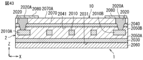
- Figures 27 to 51 show an inductor component having a roughly rectangular parallelepiped outer shape placed on a horizontal surface with the substrate side facing down, with the longitudinal direction indicated as the X-axis, the lateral direction indicated as the Y-axis, and the height direction perpendicular to these indicated as the Z-axis.
- a first magnetic layer 2030 is formed on a substrate 2060, a first insulating layer 2050A is formed on the first magnetic layer 2030, an inductor wiring 2010 and a second insulating layer 2050B covering the inductor wiring 2010 are formed on the first insulating layer 2050A, and a second magnetic layer 2040 is formed on the first insulating layer 2050A.
- the inductor wiring 2010 extends along a plane and has pad portions 2010A and 2010B at both ends. From the pad portions 2010A and 2010B at both ends, vertical wiring 2020 is formed, which extends perpendicular to the plane in which the inductor wiring 2010 extends.
- the inductor wiring 2010 is disposed between the first magnetic layer 2030 and the second magnetic layer 2040 in the Z-axis direction.
- the inductor component 1 includes an inductor element 10, pad portions 2010A and 2010B, and a vertical wiring 2020.
- the vertical wiring 2020 eliminates the need for a portion extending from the side surface of the inductor component 1 to an external terminal, and the footprint of the inductor component 1 can be reduced. As a result, the inductor component 1 can be made smaller.
- the inductor element 10 includes an element body 2, a first magnetic layer 2030, a second magnetic layer 2040, and an inductor wiring 2010 located inside the element body 2, and a substrate 2060.
- the second magnetic layer 2040 is provided along a first imaginary plane P1, the inductor wiring 2010 is provided along a second imaginary plane P2, and the first magnetic layer 2030 is provided along a third imaginary plane P3.
- the third imaginary plane P3 is parallel to the first imaginary plane P1 and the second imaginary plane P2, and the second imaginary plane P2 is located between the first imaginary plane P1 in the first direction (for example, the Z direction). That is, the inductor wiring 2010 is located between the first magnetic layer 2030 and the second magnetic layer 2040 in the first direction Z.
- This configuration can reduce leakage flux and improve the efficiency of obtaining inductance.
- “Parallel” includes “substantially parallel.”
- the roughness of the planar portion 2031 of the first magnetic layer 2030 and the roughness of the planar portion 2041 of the second magnetic layer 2040 are different from each other. This configuration can improve the freedom of material selection for the first magnetic layer 2030 and the second magnetic layer 2040. As a result, for example, the strength and adhesion of the base body 2 can be improved.
- a high-resistance silicon substrate is used as the substrate 2060.
- any other inorganic substrate (inorganic material substrate) including a glass substrate and a ceramic substrate can also be used as the substrate 2060.
- the strength of the element body 2 can be improved by including an inorganic material substrate such as a Si substrate, a glass substrate, or a ceramic substrate, which is harder than an organic resin.
- a substrate with high insulation properties is used from the viewpoint of suppressing the generation of eddy currents.
- the thickness of the substrate 2060 can be exemplified as 5 ⁇ m, but is not limited to this.
- the layers constituting the inductor component 1, including the first magnetic layer 2030 are formed on an inorganic substrate, so that the chip strength can be ensured even if it is thin.
- the substrate 2060 has a roughness smaller than that of the planar portion 2031 of the first magnetic layer 2030 and the planar portion 2041 of the second magnetic layer 2040. With this configuration, the roughness of the first insulating layer 2050A and the second insulating layer 2050B of the element body 2 can be easily adjusted.
- an inductor component 1 that does not have a substrate 2060. Also, it is possible to form an organic insulating layer between the substrate 2060 and the first magnetic layer 2030.
- the first magnetic layer 2030 and the second magnetic layer 2040 include a laminate of an inorganic insulating layer 21 and an inorganic magnetic layer 22 (see FIG. 32).
- the thickness of the first magnetic layer 2030 and the second magnetic layer 2040 can be, for example, about 5 to 6 ⁇ m, but is not limited to this.
- the material and detailed structure of the first magnetic layer 2030 and the second magnetic layer 2040 will be described in detail later in the explanation of the manufacturing method.
- the first insulating layer 2050A and the second insulating layer 2050B are formed of polyimide. However, this is not limited to this, and other organic resins such as epoxy and phenol or combinations thereof can be used, and insulating fillers may be included. Furthermore, they can be formed of inorganic insulators such as SiO 2 or TaO.
- the thickness of the first insulating layer 2050A can be exemplified as 5 ⁇ m, but is not limited to this.
- the thickness of the second insulating layer 2050B is a value obtained by adding about 2 to 10 ⁇ m to the thickness of the inductor wiring 10.
- the inductor wiring 2010 and the vertical wiring 2020 which have pads 2010A and 2010B at both ends, are made of a conductive material with low electrical resistance, such as copper, silver, or gold. A conductor containing copper or a copper compound is preferably used.
- the vertical wiring 2020 is electrically connected to the inductor wiring 2010 via the pads 2010A and 2010B at both ends.
- a rectangular wire having a cross-sectional dimension of 40 ⁇ m x 20 ⁇ m is used as the inductor wiring 2010, but this is not limited to this.
- a rectangular wire of different dimensions may also be used, and wiring other than a rectangular wire may also be used.
- the vertical length of the vertical wiring 2020 is determined by the thickness of the second insulating layer 2050B and the second magnetic layer 2040, and the amount of protrusion from the surface of the second magnetic layer 2040.
- the amount of protrusion of the vertical wiring 2020 from the surface of the second magnetic layer 2040 is 5 ⁇ m, but is not limited to this.
- L is the length in the longitudinal direction (X-axis direction)
- W is the length in the lateral direction (Y-axis direction)
- T is the length in the height direction (Z-axis direction).
- this is just one example, and inductor components with any other outer dimensions can be used.
- a current can be passed through the inductor wiring 2010 via the vertical wiring 2020 to generate a magnetic flux, allowing it to function as an inductor.
- the vertical wiring 2020 is formed so that the cross-sectional area increases from the end face in contact with the pad portions 2010A, 2010B toward the opposite end face 2020A. This improves the connection strength with the external circuit or external terminal at the end face 2020A, and suppresses the connection electrical resistance.
- the vertical wiring 2020 penetrates the second magnetic layer 2040.
- the second magnetic layer 2040 is formed so as to cover the entire periphery of the vertical wiring 2020, and the area of the second magnetic layer 2040 is maximized in the planar direction. This improves the efficiency of obtaining the inductor and suppresses leakage flux.
- multiple conductive layers are formed on the end face 2020A of the vertical wiring 2020.
- electromigration resistance can be imparted by forming a Ni layer as a conductive layer on the end face 2020A, and solder wettability can be imparted by further forming an Au layer or Sn layer, etc., as a conductive layer. This allows appropriate functionality to be imparted for connection to an external circuit.
- the first magnetic layer 2030 and the second magnetic layer 2040 which are arranged above and below the inductor wiring 2010, have uniaxial magnetic anisotropy in the same axial direction.
- the two anisotropic axes (easy axis and hard axis) of the first magnetic layer 2030 and the second magnetic layer 2040 are parallel to the longitudinal direction (X-axis direction) and the transverse direction (Y-axis direction) when the inductor component 1 is viewed in a plan view (see FIG. 26).
- the first magnetic layer 2030 and the second magnetic layer 2040 have uniaxial magnetic anisotropy in the same axial direction
- the angle between the anisotropic axes of the first magnetic layer 2030 and the second magnetic layer 2040 is within a range of less than 10 degrees.
- the anisotropy axes of the first magnetic layer 2030 and the second magnetic layer 2040 which have uniaxial magnetic anisotropy in the same axial direction, will now be described in more detail.
- the easy axis direction and hard axis direction of uniaxial magnetic anisotropy can be measured, for example, by rotating the sample by 90 degrees and measuring the magnetic layer with a VSM (vibrating sample magnetometer) to obtain a B-H curve.
- the B-H curve is also called a magnetic hysteresis curve.
- An example of a measured B-H curve is shown in Figure 28.
- the vertical axis of the graph shown in Figure 28 indicates magnetic flux density B (unit: T), and the horizontal axis indicates magnetic field strength H (unit: A/m).
- the slope of the B-H curve shown in FIG. 28 indicates the magnetic permeability ⁇ .
- the B-H curve that rises steeply indicates the easy axis (axis of easy magnetization), and the B-H curve with a gentle slope indicates the hard axis (axis of hard magnetization).
- the inductor acquisition efficiency can be improved.
- the direction of the magnetic flux generated by passing a current through the inductor wiring 2010 is parallel to the hard axis, the DC superposition characteristics can be improved or iron loss can be reduced. Note that, in order to eliminate the effects of shape anisotropy, it is preferable for the sample for testing uniaxial magnetic anisotropy to have a circular or square planar shape, but measurements can be made with other shapes as well.
- the hard axes of the first magnetic layer 2030 and the second magnetic layer 2040 which have uniaxial magnetic anisotropy, can be either in the longitudinal direction (X-axis direction) and the easy axes in the transverse direction (Y-axis direction), or, conversely, in the longitudinal direction (X-axis direction) and the hard axes in the transverse direction (Y-axis direction).
- the two ends of the inductor wiring 2010 are arranged apart in the direction of one of the hard and easy axes of the uniaxial magnetic anisotropy (X-axis direction).
- the positions of the two ends of the inductor wiring 10 in the direction of the other anisotropic axis (Y-axis direction) may be the same or different.
- the inductor wiring 2010 extends in the direction of one anisotropic axis (X-axis direction) while meandering between the pad parts 2010A and 2010B at both ends. It is worth noting here that the inductor wiring 2010 extends in the entire region without being perpendicular to one anisotropic axis (X-axis direction).
- the inductor wiring 2010 extending between the pad parts 2010A and 2010B at both ends always has a vector component in the direction of one anisotropic axis (X-axis direction). It never has a vector component in the direction of one anisotropic axis (X-axis direction) and only a vector component in the direction of the other anisotropic axis (Y-axis direction).
- the wiring center line G (see FIG. 26) passing through the center in the width direction of the inductor wiring 2010 extending without intersecting at right angles with one anisotropic axis (the X-axis direction) throughout the entire region. It can also be expressed as the angle at which the wiring center line G intersects with one anisotropic axis (the X-axis direction) is less than 90 degrees.
- this embodiment can also be described as being composed of inductor wiring 2010 of less than 0.5 turns connected together.
- the inductor wiring 2010 extends in the direction of one anisotropic axis (e.g., the X-axis direction), it has a vector component in the direction of one anisotropic axis (e.g., the X-axis direction), and so most of the magnetic flux can be directed in the direction of the other anisotropic axis (e.g., the Y-axis direction). If the inductor wiring 2010 has a region that extends perpendicular to the direction of one anisotropic axis (e.g., the X-axis direction), all of the magnetic flux in that region will be directed in the direction of one anisotropic axis (e.g., the X-axis direction), and will be affected by this.
- the inductor wiring 2010 extends in the direction of one anisotropic axis (e.g., the X-axis direction), most of the magnetic flux can be directed in the direction of the other anisotropic axis (e.g., the Y-axis direction). This provides the effect of directing the magnetic flux in the direction of the other anisotropic axis (e.g., the Y-axis direction).
- the inductor wiring 2010 extends in the entire region without intersecting at right angles with one anisotropic axis (e.g., the X-axis), the effect of one anisotropic axis (e.g., the X-axis) can be suppressed. This reliably provides the effects of improving the efficiency of inductance acquisition, improving DC superposition characteristics, or suppressing iron loss. Furthermore, since it is connected to an external circuit via the vertical wiring 2020, the inductor component 1 can be efficiently mounted.
- the anisotropic axes oriented in the longitudinal direction e.g., the X-axis direction
- the easy axis e.g., the Y-axis direction
- most of the magnetic flux passes through the hard axis (e.g., the Y-axis direction), improving the DC superposition characteristics or reducing iron loss.
- process 1 is carried out to prepare a substrate material S.
- the substrate material S is formed from high-resistivity silicon as described above.
- the thickness of the substrate material S shown in the figure is greater than the final thickness of the substrate 2060.
- a process is carried out in which multiple inductor components are formed on one substrate material S, which is then diced to obtain individual inductor components 1.
- the roughness of the surface 2061 of the substrate 2060 is adjusted by CMP, grinding and roughening treatment.
- step 2 is carried out to laminate a first magnetic layer 2030 on a substrate material S.
- the first magnetic layer 2030 includes a laminate of an inorganic insulating layer 21 and an inorganic magnetic layer 22.
- the first magnetic layer 2030 is formed, for example, by laminating the inorganic insulating layer 21 and the inorganic magnetic layer 22 in order by a sputtering method.
- the inorganic insulating layer 21 can also be referred to as a sputtered insulating layer
- the inorganic magnetic layer 22 can also be referred to as a sputtered magnetic layer.
- the inorganic magnetic layer 22 By forming the inorganic magnetic layer 22 by sputtering in a magnetic field, the atoms inside the inorganic magnetic layer 22 are arranged at the desired positions, and the easy axis direction can be oriented in the direction of the applied magnetic field. If the applied magnetic field direction is oriented in the longitudinal direction of the inductor component 1, the easy axis will be oriented in the longitudinal direction, and if the applied magnetic field direction is oriented in the transverse direction of the inductor component 1, the hard axis will be oriented in the longitudinal direction.
- the inorganic insulating layer 21 can be formed of an inorganic insulator such as SiO 2 or TaO.
- the inorganic magnetic layer 22 can be formed of CZT (Co-Zr-Ta), an FeNi alloy, or a composite of a magnetic material and an inorganic material.
- the interlayer thickness between the inorganic magnetic layers 22 may be thinner than each inorganic magnetic layer 22.
- the function of the inorganic insulating layer 21 is to insulate the inorganic magnetic layers 22 from each other or to protect the inorganic magnetic layers 22 from stress during processing, so that a thinner inorganic insulating layer 21 can increase the proportion of the magnetic layer in the entire laminate.
- the laminate structure in which the inorganic insulating layer 21 such as TaO or SiO 2 is arranged between the inorganic insulating layers 21 insulates the inorganic magnetic layers 22 from each other, suppressing eddy currents in the inorganic magnetic layers 22, thereby realizing an inductor component 1 with a high Q value at high frequencies.
- the inorganic magnetic layer 22 is made thick using CZT (Co-Zr-Ta) or an FeNi alloy, eddy currents will be generated within the magnetic layer, so in this embodiment, the inorganic magnetic layer 22 is configured to be thinner than the skin depth derived from the circuit operating frequency, for example, the switching frequency of a DCDC converter. Since the inductor is a current element, the inductor wiring 2010 is configured to have a predetermined thickness to allow a large current to flow.
- the inductor component 1 is configured so that the total thickness of the laminated inorganic magnetic layers 22 is smaller than the thickness of the inductor wiring 2010.
- the inductor wiring 2010 thicker, it is possible to realize an inductor component 1 with low DC resistance and high inductor acquisition efficiency.
- an inorganic insulating layer 21 is located on the surface of the first magnetic layer 2030. In this way, since the inorganic insulating layer 21 is located on the surface of the first magnetic layer 2030, insulation from surrounding components such as wiring can be ensured. The same is true for the second magnetic layer 2040 described below.
- step 3 is carried out to laminate a first insulating layer 2050A on the first magnetic layer 2030 formed in step 2.
- the first insulating layer 2050A can be formed by applying polyimide, which is an organic resin, to the first magnetic layer 2030 and curing it.
- step 4 is carried out to form the inductor wiring 2010 on the first insulating layer 2050A formed in step 3 using electrolytic plating.
- a seed layer containing Ti/Cu is formed on the first insulating layer 2050A using sputtering.
- a dry film resist (DFR) is then laminated on top of the seed layer, and the seed layer having a shape corresponding to the inductor wiring is exposed by photolithography. Then, power is supplied from the seed layer, and a plating portion is precipitated on the exposed seed layer using electrolytic plating to form the inductor wiring.
- the dry film resist (DFR) is then peeled off, and the seed layer is etched to obtain an insulated and independent inductor wiring. This forms the inductor wiring 2010 having a serpentine shape.
- step 5 is carried out to laminate a second insulating layer 2050B on the first insulating layer 2050A on which the inductor wiring 2010 formed in step 4 is disposed.
- the second insulating layer 2050B can be formed by applying and curing polyimide, which is an organic resin.
- the second insulating layer 2050B is formed so as to cover the side and top surfaces of the inductor wiring 2010.
- the roughness of the surface 2051B of the second insulating layer 2050B is adjusted by CMP, grinding and roughening treatment.
- step 6 is carried out to laminate the second magnetic layer 2040 on the second insulating layer 2050B formed in step 5.
- the second magnetic layer 2040 can also be laminated in the same process as the first magnetic layer 2030.
- the easy axis direction of the inorganic magnetic layer can be oriented in the direction of the applied magnetic field by a sputtering method in a magnetic field.
- the first magnetic layer 2030 and the second magnetic layer 2040 can have uniaxial magnetic anisotropy in the same axial direction.
- step 7 is carried out to form a via hole from the surface side of the second magnetic layer 2040 formed in step 6.
- laser light is irradiated from the surface side of the second magnetic layer to remove parts of the second magnetic layer 2040 and the second insulating layer 2050B, forming a via hole BH that reaches the pad portions 2010A, 2010B of the inductor wiring 2010.
- the formed via hole BH has a shape that narrows as it progresses from the surface side of the second magnetic layer to the back.
- step 8 is carried out to form vertical wiring 2020 in the via hole BH formed in step 7.
- resin residue called smear is generated.
- a desmear process is carried out to remove the smear (resin residue) generated by the laser processing.
- the vertical wiring 2020 is formed in the via hole BH.
- the vertical wiring 2020 can be formed in the via hole BH by electrolytic plating, which is the same as the method for forming the inductor wiring 2010 described above. By using electrolytic plating, a low-resistance vertical wiring 2020 can be obtained at low cost.
- the vertical wiring 2020 can also be formed by plating methods other than electrolytic plating, such as sputtering, vapor deposition, and coating.
- step 9 is carried out in which the substrate material S is ground to form a substrate 2060 of a predetermined thickness.
- step 9 can be omitted if the substrate material S has a predetermined thickness in advance.
- the substrate material S can be removed from the first magnetic layer 2030 after steps 1 to 8 are carried out. This makes it possible to obtain an inductor component 1 without a substrate, as shown in FIG. 44.
- step 9 (or step 8, depending on the case) is followed by step 10, in which the inductor components are singulated using a cutting means.
- FIG. 41 shows the inductor components 1 formed by singulation in step 10.
- a third insulating layer 2070 which is an inorganic insulating layer, is further formed on the surface of the laminated second magnetic layer 2040.
- the periphery of the side surface of the vertical wiring 2020 that intersects with the first direction Z is covered with the third insulating layer 2070.
- the third insulating layer 2070 can be formed of the same material as the first and second insulating layers 2050A and 2050B described above, or can be formed of a different material.
- the surface 2070A of the third insulating layer 2070 is formed to be at the same level as the end face 2020A of the vertical wiring 2020, and the external terminal 2080 is formed to be in contact with the surface 2070A of the third insulating layer 2070 and the end face 2020A of the vertical wiring 2020.
- the external terminal 2080 can be formed by electrolytic plating, sputtering, electroless plating, etc., in the same way as the vertical wiring 2020.
- the external terminal 2080 is positioned so as to overlap with the second magnetic layer 2040 when viewed vertically on the plane. In other words, in a planar view, the external terminal 2080 extends further outward than the second magnetic layer 2040. In this way, the external terminal 2080 is connected to the vertical wiring 2020 and extends along the plane, and the external terminal 2080 is formed so as to overlap with the second magnetic layer 2040 when viewed vertically on the plane, so that the external terminal 2080 can be made larger, reducing electrical resistance and improving adhesion strength.
- the second modified example of the inductor component 1 does not include a substrate 2060. By not having the substrate 2060, the inductor component 1 can be made thinner. Furthermore, as with the above-described first modified example, one of the vertical wirings 2020 (the vertical wiring on the left side of FIG. 44) is connected to the pad portion 2010A of the inductor wiring 2010 and is covered with a third insulating layer 2070, and an external terminal 2080 is formed on the end surface 2020A of the vertical wiring 2020.
- the other vertical wiring 2022 (the vertical wiring on the right side in FIG. 44) is connected to the surface of the pad portion 2010B of the inductor wiring 2010 on the first magnetic layer 2030 side (the lower side in FIG. 44).
- the other vertical wiring 2022 penetrates the first magnetic layer 2030 and protrudes to the outside. In this way, in the second modification, a thin inductor component 1 is realized, and since it can be connected to an external circuit from above and below, the degree of freedom in the mounting location is improved.
- the third modified example of the inductor component 1 includes a substrate 2060.
- One of the vertical wirings 2020 (the vertical wiring on the left side of FIG. 45) is covered with a third insulating layer 2070, as in the first and second modified examples, and an external terminal 2080 is formed on the end surface 2020A of the vertical wiring 2020.
- the other vertical wiring 2022 (the vertical wiring on the right side in FIG. 45) is connected to the surface of the pad portion 2010B of the inductor wiring 2010 on the first magnetic layer 2030 side (the lower side in FIG. 45), as in the second modification.
- the other vertical wiring 2022 penetrates the first magnetic layer 2030 and also the substrate 2060.
- the end surface 2022A of the other vertical wiring 2022 is disposed at the same level as the surface of the substrate 2060 and is exposed to the outside.
- the vertical wiring 2020 penetrates the substrate 2060, which is an inorganic substrate, so that it can be connected to external circuits from above and below, improving the flexibility of the mounting location, and the presence of an inorganic substrate ensures the strength of the substrate.
- the vertical wiring 2020, 2022 extends to both sides of the inductor wiring 2010, allowing connection to external circuits from above and below, improving the flexibility of the mounting location.
- each inductor wiring 2110 is formed by connecting two regions that extend parallel to one of the anisotropic axes (e.g., the X-axis direction) of the hard axis and easy axis of the uniaxial magnetic anisotropy with a region that extends in a direction intersecting the anisotropic axis (e.g., the X-axis direction).
- the region that extends in a direction intersecting the one anisotropic axis (e.g., the X-axis direction) of the inductor wiring 2110 also extends without being perpendicular to one of the anisotropic axes (e.g., the X-axis), as in the first embodiment described above.
- both ends of the inductor wiring 2110 are also arranged spaced apart in the direction of one of the hard and easy axes of the uniaxial magnetic anisotropy (e.g., the X-axis direction), and the inductor wiring 2110 extends throughout the entire region without intersecting perpendicularly with one of the anisotropic axes (e.g., the X-axis).
- a first insulating layer 2150A is laminated on a substrate 2160, and a first magnetic layer 2130 is laminated so as to be disposed between the first insulating layers 2150A.
- An inductor wiring 2110 is formed thereon, and a second insulating layer 2150B is laminated so as to cover the inductor wiring 2110, and a second magnetic layer 2140 is laminated so as to cover the second insulating layer 2150B.
- no insulating layer is formed on the second magnetic layer 2140.
- the cross-sectional dimensions of the inductor wiring 2110 can be 40 ⁇ m ⁇ 20 ⁇ m, the thickness of the substrate 2160 can be 5 ⁇ m, and the thicknesses of the first magnetic layer 2130 and the second magnetic layer 2140 can be 5 to 6 ⁇ m.
- the thickness of the first insulating layer 2150A is the thickness of the first magnetic layer 2130 plus about 2 to 10 ⁇ m.
- the thickness of the second insulating layer 2150B is the thickness of the inductor wiring 2110 plus about 2 to 10 ⁇ m.
- the amount of protrusion of the vertical wiring 2120 from the surface of the second magnetic layer 2140 can be 5 ⁇ m
- these dimensions are merely examples and are not limited to these.
- the number of inductor wirings 2110 arranged along the same plane in one inductor component 1 is two, but this is not limited to this. Any number of inductor wirings 2110, three or more, may be arranged along the same plane. In this case, an example can be given of a case where multiple inductor components 1 are arranged symmetrically with respect to a center line extending along the longitudinal direction (e.g., the X-axis direction) of the inductor component 1 having a rectangular planar shape.
- inductor wirings 2110 are arranged along the same plane, so that an inductor array element can be formed. This eliminates the need for mounting intervals, making it possible to save space.
- the non-parallel regions form regions where adjacent inductor wirings 2110 are closely spaced and arranged in parallel, and regions where adjacent inductor wirings 2110 are spaced apart and arranged in parallel.
- the coupling coefficient can be made high in the regions where adjacent inductor wirings 2110 are closely spaced, and low in the regions where adjacent inductor wirings 2110 are spaced apart.
- the second magnetic layer 2140 has an uneven shape that covers the inductor wiring 2110 from three directions.
- the second magnetic layer 2140 has an uneven shape that covers the inductor wiring 2110 from three directions, one direction of the first direction Z and two directions of the second direction Y. This allows the inductor wiring 2110 to be covered all around together with the first magnetic layer 2130, improving the efficiency of inductance acquisition.
- the inductor component 1 of FIG. in the inductor component 1 of FIG.
- the second magnetic layer 2140 has a non-planar portion 2142 that is convex or concave with respect to the first virtual plane P1.
- the first magnetic layer 2130 may be configured to have a non-planar portion.
- the planar portion 2141 of the second magnetic layer 2140 is in contact with the non-planar portion 2142.
- the planar portion 2131 of the first magnetic layer 2130 is covered with the first insulating layer 2150A.
- the second magnetic layer 2140 when viewed along the first direction Z, is provided inside the outer shape of the inductor component 1. Therefore, there is no risk of damaging the magnetic layer when cutting during individualization. For example, if the magnetic layer stretches due to mechanical stress during cutting, leakage will occur between the stacked magnetic layers, causing an increase in iron loss, but this can be avoided in this embodiment.
- the first magnetic layer 2130 and the second magnetic layer 2140 are not formed in the regions at both ends of the inductor wiring 2110 having the pad portions 2110A and 2110B. Therefore, the vertical wiring 2120 connected to the pad portions 2110A and 2110B does not penetrate the magnetic layer.
- the first magnetic layer 2130 and the second magnetic layer 2140 are disposed in the region excluding both ends of the inductor wiring 2110.
- a third insulating layer 2170 which is an inorganic insulating layer, is further formed on the surface of the laminated second magnetic layer 2140.
- the periphery of the side surface of the vertical wiring 2120 is covered with the third insulating layer 2170.
- the periphery of the uneven second magnetic layer 2140 having the non-flat portion 2142 is also covered with the third insulating layer 2170.
- Figure 49 is a cross-sectional view corresponding to Figure 47
- Figure 50 is a cross-sectional view corresponding to Figure 48.
- the surface 2170A of the third insulating layer 2170 is formed to be at the same level as the end face 2120A of the vertical wiring 2120, and the external terminal 2180 is formed to contact the surface 2170A of the third insulating layer 2170 and the end face 2120A of the vertical wiring 2120.
- the external terminal 2180 can be formed by electrolytic plating, sputtering, electroless plating, etc., as described above.
- the first magnetic layer 2130 and the second magnetic layer 2140 are covered with the first insulating layer 2150A and the second insulating layer 2150B, so that the first magnetic layer 2130 and the second magnetic layer 2140 can be protected from environmental loads (humidity, etc.).
- the surface of the third insulating layer 2170 covering the second magnetic layer 2140 which is the outermost surface of the inductor component 1, is formed flatter than the uneven shape of the second magnetic layer 2140, so that the coplanarity during mounting can be improved.
- Coplanarity means “coplanarity” and refers to the property or state in which multiple points exist along the same plane. It may also be called “surface uniformity" or "terminal flatness".
- the inductor wiring 2110 includes multiple layers arranged along the first direction Z.
- two layers consisting of two inductor wirings 2110 arranged along the same plane are formed in the first direction Z. That is, in a cross-sectional view, the inductor wirings 2110 are arranged in a 2 ⁇ 2 matrix.
- An insulating material (second insulating layer 2150B) is filled between each layer of the inductor wiring 2110.
- this is not limited to this, and a matrix-shaped inductor component 1 in which any number of inductor wirings 2110 are arranged in any number of layers along the same plane can be adopted.
- the inductor wiring 2110 extending along the plane is made up of multiple layers and insulating resin is filled between each layer of the inductor wiring 2110, the degree of freedom of the inductor wiring 2110 is improved.
- the inductor wirings 2110 by filling the spaces between the inductor wirings 2110 with insulating resin, current leakage can be suppressed and the inductor wirings 2110 can be brought closer together, resulting in a thinner inductor component 1.
- inductor component 2 element body 201 first main surface 202 second main surface 203 recess 210, 220, 230, 240 insulating layer 3 core portion 4 substrate 10 inductor element 20 magnetic layer 21 inorganic insulating layer 22 inorganic magnetic layer 23, 24 through hole 25 first end portion 26 planar portion 30 first inductor wiring 31 portion 40 second inductor wiring 50 first via portion 51 second end portion 60 second via portion 61 vertical wiring 70 external terminal 71 first external terminal 711, 712, 713, 714 terminal 72 second external terminal 721, 722 terminal 73 recess 81, 82 pad portion 811, 821 portion 90 terminal 501, 601 via opening 1000 substrate 1001 first laminate 1002 second laminate 1003 third laminate 1004 Fourth laminate 1005 Fifth laminate 1006 Sixth laminate 2010, 2110 Inductor wiring 2010A, 2010B, 2110A, 2110B Pad portion 2020, 2022, 2120 Vertical wiring 2020A, 2022A, 2120A End surface 2030, 2130 First magnetic layer 2031, 2131 Planar portion 2040, 2140 Second magnetic
Landscapes
- Engineering & Computer Science (AREA)
- Power Engineering (AREA)
- Microelectronics & Electronic Packaging (AREA)
- Coils Or Transformers For Communication (AREA)
Priority Applications (1)
| Application Number | Priority Date | Filing Date | Title |
|---|---|---|---|
| JP2025556184A JPWO2025099970A1 (https=) | 2023-11-09 | 2024-05-27 |
Applications Claiming Priority (2)
| Application Number | Priority Date | Filing Date | Title |
|---|---|---|---|
| JP2023-191738 | 2023-11-09 | ||
| JP2023191738 | 2023-11-09 |
Publications (1)
| Publication Number | Publication Date |
|---|---|
| WO2025099970A1 true WO2025099970A1 (ja) | 2025-05-15 |
Family
ID=95695223
Family Applications (1)
| Application Number | Title | Priority Date | Filing Date |
|---|---|---|---|
| PCT/JP2024/019318 Pending WO2025099970A1 (ja) | 2023-11-09 | 2024-05-27 | インダクタ素子およびインダクタ部品 |
Country Status (2)
| Country | Link |
|---|---|
| JP (1) | JPWO2025099970A1 (https=) |
| WO (1) | WO2025099970A1 (https=) |
Citations (2)
| Publication number | Priority date | Publication date | Assignee | Title |
|---|---|---|---|---|
| JPS6135976Y2 (https=) * | 1984-04-26 | 1986-10-18 | ||
| JP2008205176A (ja) * | 2007-02-20 | 2008-09-04 | Tdk Corp | 薄膜磁気デバイス及びこれを有する電子部品モジュール |
-
2024
- 2024-05-27 JP JP2025556184A patent/JPWO2025099970A1/ja active Pending
- 2024-05-27 WO PCT/JP2024/019318 patent/WO2025099970A1/ja active Pending
Patent Citations (2)
| Publication number | Priority date | Publication date | Assignee | Title |
|---|---|---|---|---|
| JPS6135976Y2 (https=) * | 1984-04-26 | 1986-10-18 | ||
| JP2008205176A (ja) * | 2007-02-20 | 2008-09-04 | Tdk Corp | 薄膜磁気デバイス及びこれを有する電子部品モジュール |
Also Published As
| Publication number | Publication date |
|---|---|
| JPWO2025099970A1 (https=) | 2025-05-15 |
Similar Documents
| Publication | Publication Date | Title |
|---|---|---|
| US12087502B2 (en) | Inductor component | |
| US11735353B2 (en) | Inductor component and method of manufacturing same | |
| JP7156209B2 (ja) | インダクタ部品およびインダクタ部品内蔵基板 | |
| JP6668723B2 (ja) | インダクタ部品 | |
| US6611035B2 (en) | Ferrite magnetic film structure having magnetic anisotropy, method of manufacturing the same, and planar magnetic device employing ferrite magnetic film structure having magenetic anisotropy | |
| JP7077835B2 (ja) | インダクタ部品 | |
| JP7334558B2 (ja) | インダクタ部品 | |
| JP7534945B2 (ja) | コイル部品 | |
| JP7722537B2 (ja) | インダクタ部品 | |
| JP7449660B2 (ja) | インダクタ部品 | |
| JP6716867B2 (ja) | コイル部品およびその製造方法 | |
| CN112652445B (zh) | 电感器部件 | |
| JP7677238B2 (ja) | 受動部品、三次元デバイスおよび受動部品の製造方法 | |
| WO2025099970A1 (ja) | インダクタ素子およびインダクタ部品 | |
| JP7494828B2 (ja) | インダクタ部品 | |
| WO2025099971A1 (ja) | インダクタ部品 | |
| WO2025099972A1 (ja) | インダクタ部品 | |
| WO2025099974A1 (ja) | インダクタ部品 | |
| WO2025099968A1 (ja) | インダクタ部品 | |
| WO2025099973A1 (ja) | インダクタ部品 | |
| CN115148450A (zh) | 线圈部件及其制造方法 | |
| JP7411590B2 (ja) | インダクタ部品およびその製造方法 | |
| US12542234B2 (en) | Inductor component and method of manufacturing inductor component | |
| JP7655276B2 (ja) | 積層型半導体パッケージおよびその製造方法 | |
| US20260128212A1 (en) | Inductor component and method of manufacturing inductor component |
Legal Events
| Date | Code | Title | Description |
|---|---|---|---|
| 121 | Ep: the epo has been informed by wipo that ep was designated in this application |
Ref document number: 24888272 Country of ref document: EP Kind code of ref document: A1 |