WO2025094343A1 - 半導体製造装置用部材 - Google Patents
半導体製造装置用部材 Download PDFInfo
- Publication number
- WO2025094343A1 WO2025094343A1 PCT/JP2023/039549 JP2023039549W WO2025094343A1 WO 2025094343 A1 WO2025094343 A1 WO 2025094343A1 JP 2023039549 W JP2023039549 W JP 2023039549W WO 2025094343 A1 WO2025094343 A1 WO 2025094343A1
- Authority
- WO
- WIPO (PCT)
- Prior art keywords
- electrode
- bias
- semiconductor manufacturing
- electrostatic
- manufacturing equipment
- Prior art date
- Legal status (The legal status is an assumption and is not a legal conclusion. Google has not performed a legal analysis and makes no representation as to the accuracy of the status listed.)
- Pending
Links
Images





Classifications
-
- H—ELECTRICITY
- H01—ELECTRIC ELEMENTS
- H01J—ELECTRIC DISCHARGE TUBES OR DISCHARGE LAMPS
- H01J37/00—Discharge tubes with provision for introducing objects or material to be exposed to the discharge, e.g. for the purpose of examination or processing thereof
- H01J37/32—Gas-filled discharge tubes
- H01J37/32431—Constructional details of the reactor
- H01J37/32532—Electrodes
- H01J37/32541—Shape
-
- H—ELECTRICITY
- H01—ELECTRIC ELEMENTS
- H01J—ELECTRIC DISCHARGE TUBES OR DISCHARGE LAMPS
- H01J37/00—Discharge tubes with provision for introducing objects or material to be exposed to the discharge, e.g. for the purpose of examination or processing thereof
- H01J37/32—Gas-filled discharge tubes
- H01J37/32431—Constructional details of the reactor
- H01J37/32532—Electrodes
- H01J37/32568—Relative arrangement or disposition of electrodes; moving means
-
- H—ELECTRICITY
- H01—ELECTRIC ELEMENTS
- H01J—ELECTRIC DISCHARGE TUBES OR DISCHARGE LAMPS
- H01J37/00—Discharge tubes with provision for introducing objects or material to be exposed to the discharge, e.g. for the purpose of examination or processing thereof
- H01J37/32—Gas-filled discharge tubes
- H01J37/32431—Constructional details of the reactor
- H01J37/32715—Workpiece holder
-
- H—ELECTRICITY
- H01—ELECTRIC ELEMENTS
- H01J—ELECTRIC DISCHARGE TUBES OR DISCHARGE LAMPS
- H01J37/00—Discharge tubes with provision for introducing objects or material to be exposed to the discharge, e.g. for the purpose of examination or processing thereof
- H01J37/32—Gas-filled discharge tubes
- H01J37/32431—Constructional details of the reactor
- H01J37/32715—Workpiece holder
- H01J37/32724—Temperature
-
- H—ELECTRICITY
- H10—SEMICONDUCTOR DEVICES; ELECTRIC SOLID-STATE DEVICES NOT OTHERWISE PROVIDED FOR
- H10P—GENERIC PROCESSES OR APPARATUS FOR THE MANUFACTURE OR TREATMENT OF DEVICES COVERED BY CLASS H10
- H10P72/00—Handling or holding of wafers, substrates or devices during manufacture or treatment thereof
- H10P72/04—Apparatus for manufacture or treatment
- H10P72/0431—Apparatus for thermal treatment
- H10P72/0432—Apparatus for thermal treatment mainly by conduction
-
- H—ELECTRICITY
- H10—SEMICONDUCTOR DEVICES; ELECTRIC SOLID-STATE DEVICES NOT OTHERWISE PROVIDED FOR
- H10P—GENERIC PROCESSES OR APPARATUS FOR THE MANUFACTURE OR TREATMENT OF DEVICES COVERED BY CLASS H10
- H10P72/00—Handling or holding of wafers, substrates or devices during manufacture or treatment thereof
- H10P72/04—Apparatus for manufacture or treatment
- H10P72/0431—Apparatus for thermal treatment
- H10P72/0434—Apparatus for thermal treatment mainly by convection
-
- H—ELECTRICITY
- H10—SEMICONDUCTOR DEVICES; ELECTRIC SOLID-STATE DEVICES NOT OTHERWISE PROVIDED FOR
- H10P—GENERIC PROCESSES OR APPARATUS FOR THE MANUFACTURE OR TREATMENT OF DEVICES COVERED BY CLASS H10
- H10P72/00—Handling or holding of wafers, substrates or devices during manufacture or treatment thereof
- H10P72/70—Handling or holding of wafers, substrates or devices during manufacture or treatment thereof for supporting or gripping
- H10P72/72—Handling or holding of wafers, substrates or devices during manufacture or treatment thereof for supporting or gripping using electrostatic chucks
-
- H—ELECTRICITY
- H10—SEMICONDUCTOR DEVICES; ELECTRIC SOLID-STATE DEVICES NOT OTHERWISE PROVIDED FOR
- H10P—GENERIC PROCESSES OR APPARATUS FOR THE MANUFACTURE OR TREATMENT OF DEVICES COVERED BY CLASS H10
- H10P72/00—Handling or holding of wafers, substrates or devices during manufacture or treatment thereof
- H10P72/70—Handling or holding of wafers, substrates or devices during manufacture or treatment thereof for supporting or gripping
- H10P72/72—Handling or holding of wafers, substrates or devices during manufacture or treatment thereof for supporting or gripping using electrostatic chucks
- H10P72/722—Details of electrostatic chucks
-
- H—ELECTRICITY
- H01—ELECTRIC ELEMENTS
- H01J—ELECTRIC DISCHARGE TUBES OR DISCHARGE LAMPS
- H01J2237/00—Discharge tubes exposing object to beam, e.g. for analysis treatment, etching, imaging
- H01J2237/002—Cooling arrangements
-
- H—ELECTRICITY
- H01—ELECTRIC ELEMENTS
- H01J—ELECTRIC DISCHARGE TUBES OR DISCHARGE LAMPS
- H01J2237/00—Discharge tubes exposing object to beam, e.g. for analysis treatment, etching, imaging
- H01J2237/20—Positioning, supporting, modifying or maintaining the physical state of objects being observed or treated
- H01J2237/2007—Holding mechanisms
Definitions
- the present invention relates to components for semiconductor manufacturing equipment.
- a semiconductor manufacturing equipment component that includes a ceramic plate having a wafer mounting surface on its upper surface and a built-in electrode, a base plate provided on the underside of the ceramic plate, and a gas passageway provided so as to extend from the underside of the base plate to the wafer mounting surface of the ceramic plate.
- a cylindrical shield electrode portion is provided around the gas passageway in such a semiconductor manufacturing equipment component in the ceramic plate.
- the cylindrical shield electrode portion has a shielding function to prevent the influence of the electric field generated around the electrostatic electrode when a DC voltage is applied to the electrostatic electrode from reaching the internal space of the gas passageway. This prevents or reduces the occurrence of abnormal discharge in the gas passageway.
- Patent Document 1 if the shielding provided by the shield electrode portion is insufficient, it may not be possible to prevent abnormal discharges from occurring in the gas passage.
- the present invention was made to solve the above-mentioned problems, and its main purpose is to prevent or reduce the occurrence of abnormal discharges in the passageway using a different principle than conventional methods.
- the semiconductor manufacturing equipment member of the present invention comprises: a ceramic plate having a wafer mounting surface on an upper surface thereof and incorporating an electrostatic electrode; a base plate provided on a lower surface of the ceramic plate and having a coolant flow path built therein; a passage extending from a lower surface of the base plate to the wafer mounting surface of the ceramic plate; at least one internal electrode provided inside the ceramic plate, surrounding the passage below the electrostatic electrode and not exposed to an inner wall of the passage, and electrically connected to the electrostatic electrode; a bias electrode that is provided electrically independent of the electrostatic electrode at a position equal to or lower than a lowermost internal electrode among the at least one internal electrode, and to which a bias voltage is applied when plasma is generated above the wafer mounting surface; It is equipped with the following:
- At least one internal electrode electrically connected to the electrostatic electrode is provided inside the ceramic plate so as to surround the passage below the electrostatic electrode and not be exposed to the inner wall of the passage.
- a DC voltage is applied to the electrostatic electrode and a bias voltage is applied to the bias electrode
- a potential gradient is generated in the vertical direction in the internal space of the passage.
- the vertical distance over which the potential gradient is generated is shorter than when no internal electrode is provided.
- “upper” and “lower” do not represent absolute positional relationships, but rather relative positional relationships. Therefore, depending on the orientation of the semiconductor manufacturing equipment component, “upper” and “lower” may become “lower” and “upper,” “left” and “right,” or “front” and “rear.” Furthermore, examples of “passages” include gas passages and lift pin holes. Furthermore, when there is only one “internal electrode,” that "internal electrode” becomes the “lowest internal electrode.”
- the base plate may also serve as the bias electrode. This eliminates the need to provide a bias electrode separate from the base plate.
- the bias electrode may be built into the ceramic plate.
- the bias electrode may be provided below the lowermost internal electrode.
- the bias electrode may be provided at the same height as the lowermost internal electrode and may be provided around the lowermost internal electrode.
- the at least one internal electrode may be a ring-shaped electrode surrounding the passage, or an electrode having the same shape as the electrostatic electrode and a through-hole through which the passage passes.
- the internal electrode is a ring-shaped electrode, the amount of electrode material used can be reduced.
- the internal electrode has the same shape as the electrostatic electrode, the internal electrode has a relatively large area, so there is a high degree of freedom in designing the wiring that electrically connects the internal electrode and the electrostatic electrode.
- the same shape means that the shapes (e.g., circular or rectangular) are the same, and the sizes may be the same or different.
- the passage may be connected to a heat transfer gas supply source.
- the atoms or molecules of the heat transfer gas are ionized in the internal space of the passage to generate electrons, and these electrons are likely to collide with other atoms or molecules, making it highly significant to apply the present invention.
- the base plate may also serve as a source electrode to which a source voltage is applied when generating plasma above the wafer placement surface. This eliminates the need to provide a source electrode separate from the base plate.
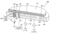
- FIG. FIG. 2 is a perspective view with a cross-sectional view of the wafer mounting table 10;
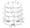
- FIG. FIG. 2 is a perspective view showing the positional relationship between the electrostatic electrode 22 and the first to fourth internal electrodes 31 to 34.
- FIG. FIG. FIG. 11 is a perspective view showing the positional relationship of each electrode according to another embodiment.
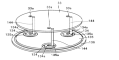
- FIG. 11 is a perspective view showing the positional relationship of each electrode according to another embodiment.
- FIG. 11 is a perspective view showing the positional relationship of each electrode according to another embodiment.
- Fig. 1 is a plan view of the wafer mounting table 10
- Fig. 2 is a perspective view with a cross-section of the wafer mounting table 10
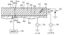
- Fig. 3 is a partial cross-section of the wafer mounting table 10
- Fig. 4 is a perspective view showing the positional relationship of the electrostatic electrode 22 and the first to fourth internal electrodes 31 to 34.
- the seal band 21a and small circular protrusions 21b are omitted in Figs. 2 and 3.
- the first to fourth internal electrodes 31 to 34 are omitted in Fig. 2, and the electrode terminal 26, power supply member 58, and power supply member arrangement hole 54 are omitted in Fig. 3.
- the wafer mounting table 10 is an example of a semiconductor manufacturing device component of the present invention, and as shown in FIG. 2, it includes a ceramic plate 20, a base plate 50, a bonding layer 60, a power supply member placement hole 54, and a gas passage 24.
- the ceramic plate 20 is a ceramic circular plate (e.g., 300 mm in diameter, 5 mm in thickness) made of alumina sintered body or aluminum nitride sintered body.
- the upper surface of the ceramic plate 20 is the wafer mounting surface 21.
- the ceramic plate 20 has an electrostatic electrode 22 built in.
- the wafer mounting surface 21 has a seal band 21a formed along the outer edge, and a plurality of circular small protrusions 21b formed on the entire inner surface of the seal band 21a.
- the seal band 21a and the circular small protrusions 21b have the same height, and the height is, for example, several ⁇ m to several tens of ⁇ m.
- the electrostatic electrode 22 is a circular mesh flat electrode, and is connected to the DC power supply 70 via the power supply member 58.
- a DC voltage is applied to the electrostatic electrode 22
- the wafer W is attracted and fixed to the wafer mounting surface 21 (specifically, the upper surface of the seal band 21a and the upper surface of the circular small protrusions 21b) by electrostatic attraction force, and when the application of the DC voltage is released, the wafer W is released from the wafer mounting surface 21.
- first to fourth internal electrodes 31 to 34 are provided in order from top to bottom, with the fourth internal electrode 34 being located at the bottom.
- the first to fourth internal electrodes 31 to 34 are all provided below the electrostatic electrode 22.
- the first to fourth internal electrodes 31 to 34 are provided inside the ceramic plate 20 so as to surround the gas passage 24 and not be exposed to the inner wall of the gas passage 24.
- the first to fourth internal electrodes 31 to 34 are circular mesh planar electrodes of the same shape as the electrostatic electrode 22, and are approximately the same size as the electrostatic electrode 22.
- the electrostatic electrode 22 and the first internal electrode 31 are electrically connected by a first via 41 extending in the vertical direction
- the first internal electrode 31 and the second internal electrode 32 are electrically connected by a second via 42 extending in the vertical direction
- the second internal electrode 32 and the third internal electrode 33 are electrically connected by a third via 43 extending in the vertical direction
- the third internal electrode 33 and the fourth internal electrode 34 are electrically connected by a fourth via 44 extending in the vertical direction. Therefore, the first to fourth internal electrodes 31 to 34 have the same potential as the electrostatic electrode 22.
- the first to fourth vias 41 to 44 are not aligned in a straight line when viewed in the vertical direction, but are aligned in a shifted manner. As shown in FIG.
- the distance D1 between the electrostatic electrode 22 and the first internal electrode 31, the distance D2 between the first internal electrode 31 and the second internal electrode 32, the distance D3 between the second internal electrode 32 and the third internal electrode 33, the distance D4 between the third internal electrode 33 and the fourth internal electrode 34, and the distance Db between the fourth internal electrode 34 and the lower surface of the ceramic plate 20 are preferably at least one time the distance d between the wafer mounting surface 21 and the electrostatic electrode 22.
- the base plate 50 is a circular plate with good electrical conductivity and thermal conductivity (e.g., a circular plate with the same diameter as or larger than the ceramic plate 20, 25 mm thick) and is electrically independent of the electrostatic electrode 22 and the first to fourth internal electrodes 31 to 34.
- a refrigerant flow path 52 through which a refrigerant circulates is provided inside the base plate 50.
- the refrigerant flowing through the refrigerant flow path 52 is preferably a liquid, and is preferably electrically insulating. Examples of electrically insulating liquids include fluorine-based inert liquids. As shown in FIG.
- the refrigerant flow path 52 is formed in a spiral shape in a plan view from one end (inlet 52in) to the other end (outlet 52out) over the entire base plate 50.
- the inlet 52in and outlet 52out of the refrigerant flow path 52 are connected to a supply port and a recovery port of an external refrigerant device (not shown), respectively.
- the coolant supplied from the supply port of the external coolant device to the inlet 52in of the coolant flow passage 52 passes through the coolant flow passage 52, returns from the outlet 52out of the coolant flow passage 52 to the recovery port of the external coolant device, and is supplied again from the supply port to the inlet 52in of the coolant flow passage 52 after being temperature-adjusted.
- the base plate 50 is connected to a source power supply 72 and a bias power supply 74.
- the source power supply 72 is a power supply that generates a source RF for generating plasma above the wafer mounting surface 21.
- the bias power supply 74 is a power supply that generates a bias RF for attracting ions to the wafer W.
- the bias RF has a lower frequency and a larger amplitude than the source RF.
- the bias RF may be a sine wave (positive and negative alternately appearing) or a square wave (negative squares appearing periodically), but a square wave is preferable for sharp etching.
- the frequency of the source RF is, for example, several tens to several hundreds of MHz, and the frequency of the bias RF is, for example, several hundred kHz.
- the material of the base plate 50 may be, for example, a metal material or a composite material of metal and ceramic.
- the metal material may be Al, Ti, Mo, or an alloy thereof.
- the composite material of metal and ceramic may be a metal matrix composite material (MMC) or a ceramic matrix composite material (CMC).
- MMC metal matrix composite material
- CMC ceramic matrix composite material
- Specific examples of such composite materials include a material containing Si, SiC, and Ti (also called SiSiCTi), a material in which a SiC porous body is impregnated with Al and/or Si, and a composite material of Al2O3 and TiC. It is preferable to select a material of the base plate 50 having a thermal expansion coefficient close to that of the material of the ceramic plate 20.
- the bonding layer 60 is a metal bonding layer, which bonds the lower surface of the ceramic plate 20 and the upper surface of the base plate 50.
- the metal bonding layer may be, for example, a layer formed of solder or metal brazing material.
- the metal bonding layer is formed, for example, by TCB (thermal compression bonding).
- TCB refers to a known method in which a metal bonding material is sandwiched between two members to be bonded, and the two members are pressurized and bonded while being heated to a temperature below the solidus temperature of the metal bonding material.
- the bonding layer 60 may be a resin adhesive layer. Examples of materials for the resin adhesive layer include insulating resins such as epoxy resin, acrylic resin, and silicone resin, as well as insulating resins containing fillers.
- the power supply member arrangement hole 54 is a substantially cylindrical hole that penetrates the base plate 50 and the bonding layer 60 in the vertical direction, and is provided so as not to penetrate the refrigerant flow path 52.
- An insulating tube 56 is housed in the power supply member arrangement hole 54.
- the insulating tube 56 is fixed to the power supply member arrangement hole 54 by adhesive.
- An electrode terminal 26 electrically connected to the electrostatic electrode 22 is exposed at the upper bottom of the power supply member arrangement hole 54.
- a power supply member 58 is electrically connected to the electrode terminal 26.
- the power supply member 58 is a flexible metal wire 58c connecting an upper metal terminal 58a and a lower metal terminal 58b, and the upper metal terminal 58a is joined to the electrode terminal 26.
- the lower metal terminal 58b is exposed from the lower opening of the insulating tube 56 and is connected to a DC power source 70 for electrostatic adsorption.
- the power supply member 58 may be a metal rod.
- the gas passage 24 is a substantially cylindrical hole that passes through the base plate 50, the bonding layer 60, and the ceramic plate 20 in the vertical direction, and is provided so as not to pass through the refrigerant flow path 52.
- the gas passage 24 is connected to a He gas supply source 76.
- the gas passage 24 is provided so as to extend from the lower surface of the base plate 50 to the wafer mounting surface 21.
- An insulating tube 57 is housed in the portion of the gas passage 24 that passes through the base plate 50 and the bonding layer 60.
- the insulating tube 57 is fixed to the gas passage 24 by adhesive.
- the gas passage 24 passes through the electrostatic electrode 22 and the first to fourth internal electrodes 31 to 34 in the vertical direction.
- Through holes 22a, 31a to 34a with a diameter larger than the diameter of the gas passage 24 are provided in the portion of the electrostatic electrode 22 through which the gas passage 24 passes and in the portion of the first to fourth internal electrodes 31 to 34 through which the gas passage 24 passes. Therefore, the electrostatic electrode 22 and the first to fourth internal electrodes 31 to 34 are not exposed to the inner wall of the gas passage 24.
- the length L between the gas passage 24 and the through hole 22a of the electrostatic electrode 22 is preferably at least twice the distance d between the wafer mounting surface 21 and the electrostatic electrode 22.
- the length between the gas passage 24 and the through holes 31a to 34a of the first to fourth internal electrodes 31 to 34 is also preferably at least twice the distance d.
- the ceramic plate 20 can be obtained by, for example, preparing six molded sheets, processing each molded sheet, stacking them, hot-pressing them, and then performing shaping (such as drilling holes).
- the first molded sheet from the top is used as is without processing.
- conductive paste is printed on the top surface so that it has the same shape as the electrostatic electrode 22, and a via filled with conductive paste is provided at the position of the first via 44.
- conductive paste is printed on the top surface so that it has the same shape as the first to third internal electrodes 31 to 33, and vias filled with conductive paste are provided at the positions of the second to fourth vias 42 to 44.
- conductive paste is printed on the top surface so that it has the same shape as the fourth internal electrode 34.
- Each molded sheet can be produced by tape molding or mold cast molding. These six sheets are then stacked and hot-pressed and then shaped (such as by drilling holes). The gas passages 24 may be formed before or after the hot-press firing.
- the wafer W is placed on the wafer mounting surface 21 with the wafer mounting table 10 installed in a chamber (not shown).
- the chamber is then depressurized by a vacuum pump to adjust the pressure to a predetermined degree of vacuum, and a DC voltage is applied to the electrostatic electrode 22 of the ceramic plate 20 to generate an electrostatic adsorption force, thereby adsorbing and fixing the wafer W to the wafer mounting surface 21.
- He gas is also supplied to the gas passage 24 from the He gas supply source 76. The He gas is filled in the space surrounded by the seal band 21a, the circular small protrusions 21b, and the wafer W.
- a reaction gas atmosphere of a predetermined pressure (for example, several tens to several hundreds of Pa) is created in the chamber, and in this state, a source voltage from the source power source 72 and a bias voltage from the bias power source 74 are applied to the base plate 50.
- plasma is generated between an upper electrode (not shown) installed on the ceiling of the chamber and the wafer mounting surface 21 of the wafer mounting table 10. The surface of the wafer W is processed by the generated plasma.
- a coolant is circulated in the coolant flow passage 52 of the base plate 50 at appropriate times.
- a potential gradient from positive to negative is generated in the vertical direction due to the application of a DC voltage to the electrostatic electrode 22 and the application of a bias voltage to the base plate 50, which is a bias electrode.
- the first to fourth internal electrodes 31 to 34 which have the same potential as the electrostatic electrode 22, are provided inside the ceramic plate 20. Therefore, no potential gradient is generated in the vertical direction between the electrostatic electrode 22 and the fourth internal electrode 34 in the internal space of the gas passage 24.
- a potential gradient from positive to negative is generated between the fourth internal electrode 34 and the base plate 50, which is a bias electrode, but the vertical length over which the potential gradient is generated is short, being approximately the same as the distance between the fourth internal electrode 34 and the base plate 50. Therefore, even if electrons generated as a result of the ionization of He atoms accelerate and hit other He atoms in the internal space of the gas passage 24, the electrons do not acquire high energy because the distance of acceleration is short, and abnormal discharge does not occur even if they hit other He atoms.
- the vertical length along which a potential gradient occurs in the internal space of the gas passage 24 is longer than in this embodiment. Therefore, if electrons generated as a result of the ionization of He atoms in the internal space of the gas passage 24 accelerate and collide with other He atoms, the electrons will have high energy due to the long acceleration distance, and these electrons will collide with other He atoms, ionizing the He atoms and generating further electrons. This phenomenon is likely to occur repeatedly, making it easy for abnormal discharge to occur.
- the first to fourth internal electrodes 31 to 34 electrically connected to the electrostatic electrode 22 are provided inside the ceramic plate 20 so as to surround the gas passage 24 below the electrostatic electrode 22 and not be exposed to the inner wall of the gas passage 24.
- the electrostatic electrode 22 has a positive potential when a DC voltage is applied when the wafer W is attracted to the wafer mounting surface 21.
- the base plate 50 which is a bias electrode, has a periodic negative potential when a bias voltage is applied to attract ions in the plasma. Therefore, a potential with a positive to negative gradient is generated in the internal space of the gas passage 24 in the vertical direction.
- the first to fourth internal electrodes 31 to 34 are provided below the electrostatic electrode 22, so that the vertical distance over which the potential gradient is generated is shortened. As a result, even if electrons are generated by ionization from He atoms, they are not sufficiently accelerated by the potential gradient and do not have sufficient energy, so arc discharge can be avoided. Therefore, the occurrence of abnormal discharge in the gas passage 24 can be prevented or reduced.
- the base plate 50 also serves as a bias electrode. Therefore, there is no need to provide a bias electrode separate from the base plate 50.
- first to fourth internal electrodes 31 to 34 have the same shape as the electrostatic electrode 22 (circular planar electrodes) and a relatively large area, which increases the degree of freedom in designing the first to fourth vias 41 to 44.
- the size of the first to fourth internal electrodes 31 to 34 may be the same as, slightly larger than, or slightly smaller than the electrostatic electrode 22.
- the gas passage 24 is connected to a He gas supply source 76. Therefore, in the internal space of the gas passage 24, He atoms are ionized to generate electrons, and these electrons are likely to collide with other He atoms, making the application of the present invention highly meaningful.
- the base plate 50 also serves as a source electrode. Therefore, there is no need to provide a source electrode separate from the base plate 50.
- first to fourth vias 41 to 44 are not aligned in a straight line when viewed in the vertical direction, but are aligned in a shifted manner. In this case, compared to when the first to fourth vias 41 to 44 are aligned in a straight line in the vertical direction, this is more preferable because it reduces the risk of cracks occurring at the locations where the first to fourth vias 41 to 44 are provided due to the difference in thermal expansion between ceramic and metal when manufacturing the ceramic plate 20 by firing. In other words, in this embodiment, since the first to fourth vias 41 to 44 are aligned in a shifted manner when viewed in the vertical direction, the difference in thermal expansion during firing is reduced, and cracks are less likely to occur at the locations where the first to fourth vias 41 to 44 are provided.
- the base plate 50 also serves as the bias electrode, but the bias electrode may be built into the ceramic plate 20.
- FIG. 5 shows an example in which a bias electrode 35 is provided instead of the fourth internal electrode 34 of the above-mentioned embodiment.
- the bias electrode 35 is not electrically connected to the electrostatic electrode 22 or the first to third internal electrodes 31 to 33, but is connected to a bias power supply 74.
- a through hole 35a having a diameter larger than the diameter of the gas passage 24 is provided in the portion of the bias electrode 35 through which the gas passage 24 passes. Therefore, the bias electrode 35 is not exposed to the inner wall of the gas passage 24.
- the length between the gas passage 24 and the through hole 35a of the bias electrode 35 is preferably at least twice the distance d between the wafer mounting surface 21 and the electrostatic electrode 22.
- the distance between the bias electrode 35 and the lower surface of the ceramic plate 20 is preferably at least one time the distance d.
- the first to third internal electrodes 31 to 33 which have the same potential as the electrostatic electrode 22, are provided below the electrostatic electrode 22, so the vertical distance over which the potential gradient occurs is shorter than when the first to third internal electrodes 31 to 33 are not present. This makes it possible to prevent or reduce the occurrence of abnormal discharge in the gas passage 24.
- FIGS. 6 and 7 show an example in which a ring-shaped fourth internal electrode 134 is used instead of the fourth internal electrode 34 of the above-mentioned embodiment, and a bias electrode 135 is embedded in the ceramic plate 20 so as to surround the fourth internal electrode 134.
- the fourth internal electrode 134 is provided so as to surround the gas passage 24.
- a through hole 134a having a diameter larger than the diameter of the gas passage 24 is provided in the portion of the fourth internal electrode 134 through which the gas passage 24 passes. Therefore, the fourth internal electrode 134 is not exposed to the inner wall of the gas passage 24.
- the fourth internal electrode 134 is electrically connected to the third internal electrode 33 through a via 144. Therefore, the fourth internal electrode 134 has the same potential as the electrostatic electrode 22.
- the bias electrode 135 is provided on the same plane as the fourth internal electrode 134, is not electrically connected to the electrostatic electrode 22 or the first to fourth internal electrodes 31 to 33, 134, and is connected to the bias power supply 74.
- the bias electrode 135 has a through hole 135a provided at a distance from the fourth internal electrode 134.
- the distance between the third internal electrode 33 and the fourth internal electrode 134 (or the bias electrode 135) is preferably at least one time the distance d between the wafer mounting surface 21 and the electrostatic electrode 22.
- the length between the gas passage 24 and the through hole 134a of the fourth internal electrode 134 and the distance between the outer edge of the fourth internal electrode 134 and the inner edge of the through hole 135a are preferably at least twice the distance d.
- the first to fourth internal electrodes 31 to 33, 134 which have the same potential as the electrostatic electrode 22, are provided below the electrostatic electrode 22, so the vertical distance over which the potential gradient occurs is shorter than when the first to fourth internal electrodes 31 to 33, 134 are not present. Therefore, it is possible to prevent or reduce the occurrence of abnormal discharge in the gas passage 24.
- FIG. 8 shows an example in which an external bias electrode 136 is provided on the outer periphery of the bias electrode 135 in FIG. 7.
- the external bias electrode 136 is a ring-shaped electrode provided on the same plane as the circular bias electrode 135, and is not electrically connected to the electrostatic electrode 22, the first to fourth internal electrodes 31 to 33, 134, or the bias electrode 135.
- the distance between the inner edge of the external bias electrode 136 and the outer edge of the bias electrode 135 is preferably at least twice the distance d.
- different bias voltages can be applied to the bias electrode 135 and the external bias electrode 136. Therefore, the degree of ion attraction can be changed between the center side and the outer periphery side of the wafer W.
- the focus ring is placed on a step provided along the outer periphery of the ceramic plate 20, the degree to which ions are attracted to the focus ring and the wafer W can be changed.
- the first to fourth internal electrodes 31 to 34 have the same shape as the electrostatic electrode 22, but the first to fourth internal electrodes 31 to 34 may be ring-shaped electrodes surrounding the gas passage 24.
- An example is shown in FIG. 9.
- the first internal electrodes 31 are ring-shaped electrodes, and the number of the first internal electrodes 31 is formed on the same plane according to the number of gas passages 24 (see FIG. 1). All the first internal electrodes 31 are electrically connected by wiring 31b, and one of the first internal electrodes 31 is connected to the electrostatic electrode 22 via the first via 41.
- the second internal electrodes 32 are ring-shaped electrodes, and the number of the second internal electrodes 32 is formed on the same plane according to the number of gas passages 24. All the second internal electrodes 32 are electrically connected by wiring 32b, and one of the second internal electrodes 32 is connected to the first internal electrode 31 via the second via 42.
- the third internal electrodes 33 are ring-shaped electrodes, and the number of the third internal electrodes 33 corresponds to the number of the gas passages 24. All the third internal electrodes 33 are electrically connected by wiring 33b, and one of the third internal electrodes 33 is connected to the second internal electrode 32 through the third via 43.
- the fourth internal electrodes 34 are ring-shaped electrodes, and the number of the fourth internal electrodes 34 corresponds to the number of the gas passages 24.
- All the fourth internal electrodes 34 are electrically connected by wiring 34b, and one of the fourth internal electrodes 34 is connected to the third internal electrode 33 through the fourth via 44. Therefore, all the first to fourth internal electrodes 31 to 34 have the same potential as the electrostatic electrode 22. Even in this case, the same effect as the above-mentioned embodiment can be obtained.
- the first via 41 may be provided on the wiring 31b instead of on the first internal electrode 31. This is also true for the second to fourth vias 42 to 44. Also, the wiring 31b may be omitted, and the first via 41 may be provided in each of the first internal electrodes 31. This also applies to the second to fourth vias 42 to 44. Also, some of the first to fourth internal electrodes 31 to 34 may be ring-shaped electrodes, and the rest may be electrodes of the same shape as the electrostatic electrode 22.
- the first to fourth internal electrodes 31 to 34 are provided inside the ceramic plate 20, but the number of internal electrodes may be at least one. For example, only the fourth internal electrode 34 may be provided inside the ceramic plate 20.
- the electrostatic electrode 22 is built into the ceramic plate 20, but this is not particularly limited.
- a heater electrode resistive heating element
- a heater electrode resistive heating element
- a porous plug (a plug that allows gas to flow in the vertical direction) may be provided in the gas passage 24 at a location where potential distribution occurs.
- a dense plug having a zigzag or spiral passage (a passage that allows gas to flow in the vertical direction) may be used. This makes it easier to prevent abnormal discharge from occurring at the location where potential distribution occurs.
- gas passages 24 are provided, but the number of gas passages 24 is not limited to this, and may be any number.
- the gas passages 24 are described as passages that penetrate the wafer mounting table 10 in the vertical direction, but the number of gas passages 24 is not limited to this.
- a gas channel structure may be adopted instead of the gas passages 24.
- the gas channel structure a structure including a ring-shaped passage that is provided inside the base plate 50 and is concentric with the base plate 50 in a plan view, a gas introduction passage that introduces gas from the lower surface of the base plate 50 to the ring-shaped passage, and a plurality of gas distribution passages that extend upward from the ring-shaped passage and open to the wafer mounting surface 21 may be adopted.
- the number of gas introduction passages may be less than the number of gas distribution passages, and may be, for example, one.
- Such a gas channel structure also corresponds to the "passage" of the present invention.
- lift pin holes may be provided separately from the gas passage 24.
- the lift pin holes are holes that penetrate the wafer mounting table 10 in the vertical direction and allow the insertion of lift pins that move the wafer W up and down relative to the wafer mounting surface 21.
- three lift pin holes are provided.
- the configuration of the lift pin holes and their surroundings is the same as the configuration of the gas passage 24 and its surroundings.
- the lift pin holes are provided so as to reach the wafer mounting surface 21 from the underside of the ceramic plate 20. Therefore, He gas also enters the lift pin holes, but like the gas passage 24, the occurrence of abnormal discharge in the lift pin holes can be prevented or reduced.
- Such lift pin holes also correspond to the "passage" of the present invention.
- the DC power supply 70 is connected to the electrostatic electrode 22, but instead, the DC power supply 70 may be connected to any one of the first to fourth internal electrodes 31 to 34.
- the semiconductor manufacturing equipment components of the present invention can be used, for example, in fields where wafers are processed with plasma, etc.
- 10 wafer mounting table 20 ceramic plate, 21 wafer mounting surface, 21a seal band, 21b small circular protrusion, 22 electrostatic electrode, 22a through hole, 24 gas passage, 26 electrode terminal, 31-34 first to fourth internal electrodes, 31a-34a through hole, 31b-34b wiring, 35 bias electrode, 35a through hole, 41-44 first to fourth vias, 50 base plate, 52 coolant flow path, 52in Inlet, 52out outlet, 54 power supply member placement hole, 56, 57 insulating tube, 58 power supply member, 58a upper metal terminal, 58b lower metal terminal, 58c metal wire, 60 bonding layer, 70 DC power supply, 72 source power supply, 74 bias power supply, 76 He gas supply source, 134 fourth internal electrode, 134a through hole, 135 bias electrode, 135a through hole, 136 outer bias electrode, 144 fourth via.
Landscapes
- Physics & Mathematics (AREA)
- Engineering & Computer Science (AREA)
- Plasma & Fusion (AREA)
- Chemical & Material Sciences (AREA)
- Analytical Chemistry (AREA)
- Container, Conveyance, Adherence, Positioning, Of Wafer (AREA)
- Jigs For Machine Tools (AREA)
Priority Applications (4)
| Application Number | Priority Date | Filing Date | Title |
|---|---|---|---|
| JP2024534111A JP7704985B1 (ja) | 2023-11-02 | 2023-11-02 | 半導体製造装置用部材 |
| PCT/JP2023/039549 WO2025094343A1 (ja) | 2023-11-02 | 2023-11-02 | 半導体製造装置用部材 |
| TW113115955A TW202520417A (zh) | 2023-11-02 | 2024-04-29 | 半導體製造裝置用零件 |
| US18/735,576 US20250149370A1 (en) | 2023-11-02 | 2024-06-06 | Member for semiconductor manufacturing apparatus |
Applications Claiming Priority (1)
| Application Number | Priority Date | Filing Date | Title |
|---|---|---|---|
| PCT/JP2023/039549 WO2025094343A1 (ja) | 2023-11-02 | 2023-11-02 | 半導体製造装置用部材 |
Related Child Applications (1)
| Application Number | Title | Priority Date | Filing Date |
|---|---|---|---|
| US18/735,576 Continuation US20250149370A1 (en) | 2023-11-02 | 2024-06-06 | Member for semiconductor manufacturing apparatus |
Publications (1)
| Publication Number | Publication Date |
|---|---|
| WO2025094343A1 true WO2025094343A1 (ja) | 2025-05-08 |
Family
ID=95561712
Family Applications (1)
| Application Number | Title | Priority Date | Filing Date |
|---|---|---|---|
| PCT/JP2023/039549 Pending WO2025094343A1 (ja) | 2023-11-02 | 2023-11-02 | 半導体製造装置用部材 |
Country Status (4)
| Country | Link |
|---|---|
| US (1) | US20250149370A1 (https=) |
| JP (1) | JP7704985B1 (https=) |
| TW (1) | TW202520417A (https=) |
| WO (1) | WO2025094343A1 (https=) |
Citations (5)
| Publication number | Priority date | Publication date | Assignee | Title |
|---|---|---|---|---|
| JP2005136350A (ja) * | 2003-10-31 | 2005-05-26 | Tokyo Electron Ltd | 静電吸着装置、プラズマ処理装置及びプラズマ処理方法 |
| US20170352567A1 (en) * | 2016-06-07 | 2017-12-07 | Applied Materials, Inc. | High power electrostatic chuck design with radio frequency coupling |
| JP2020205379A (ja) * | 2019-06-18 | 2020-12-24 | 東京エレクトロン株式会社 | 載置台及びプラズマ処理装置 |
| JP2022119239A (ja) * | 2021-02-04 | 2022-08-17 | 日本碍子株式会社 | 半導体製造装置用部材及びその製法 |
| JP2023044634A (ja) * | 2021-09-17 | 2023-03-30 | 東京エレクトロン株式会社 | プラズマ処理装置 |
Family Cites Families (6)
| Publication number | Priority date | Publication date | Assignee | Title |
|---|---|---|---|---|
| EP3098838B1 (en) * | 2014-01-22 | 2021-01-27 | ULVAC, Inc. | Plasma treatment device and wafer transportation tray |
| JP7677862B2 (ja) * | 2021-09-17 | 2025-05-15 | 東京エレクトロン株式会社 | プラズマ処理装置 |
| TW202326801A (zh) * | 2021-11-26 | 2023-07-01 | 日商東京威力科創股份有限公司 | 靜電吸盤及電漿處理裝置 |
| JP7554220B2 (ja) * | 2022-03-08 | 2024-09-19 | 日本碍子株式会社 | 半導体製造装置用部材 |
| JP7622002B2 (ja) * | 2022-03-31 | 2025-01-27 | 日本碍子株式会社 | ウエハ載置台 |
| WO2025094344A1 (ja) * | 2023-11-02 | 2025-05-08 | 日本碍子株式会社 | 半導体製造装置用部材 |
-
2023
- 2023-11-02 JP JP2024534111A patent/JP7704985B1/ja active Active
- 2023-11-02 WO PCT/JP2023/039549 patent/WO2025094343A1/ja active Pending
-
2024
- 2024-04-29 TW TW113115955A patent/TW202520417A/zh unknown
- 2024-06-06 US US18/735,576 patent/US20250149370A1/en active Pending
Patent Citations (5)
| Publication number | Priority date | Publication date | Assignee | Title |
|---|---|---|---|---|
| JP2005136350A (ja) * | 2003-10-31 | 2005-05-26 | Tokyo Electron Ltd | 静電吸着装置、プラズマ処理装置及びプラズマ処理方法 |
| US20170352567A1 (en) * | 2016-06-07 | 2017-12-07 | Applied Materials, Inc. | High power electrostatic chuck design with radio frequency coupling |
| JP2020205379A (ja) * | 2019-06-18 | 2020-12-24 | 東京エレクトロン株式会社 | 載置台及びプラズマ処理装置 |
| JP2022119239A (ja) * | 2021-02-04 | 2022-08-17 | 日本碍子株式会社 | 半導体製造装置用部材及びその製法 |
| JP2023044634A (ja) * | 2021-09-17 | 2023-03-30 | 東京エレクトロン株式会社 | プラズマ処理装置 |
Also Published As
| Publication number | Publication date |
|---|---|
| JP7704985B1 (ja) | 2025-07-08 |
| TW202520417A (zh) | 2025-05-16 |
| JPWO2025094343A1 (https=) | 2025-05-08 |
| US20250149370A1 (en) | 2025-05-08 |
Similar Documents
| Publication | Publication Date | Title |
|---|---|---|
| JP7620578B2 (ja) | 半導体製造装置用部材 | |
| CN116344428B (zh) | 半导体制造装置用部件 | |
| CN115954310B (zh) | 半导体制造装置用部件 | |
| US12211729B2 (en) | Member for semiconductor manufacturing apparatus | |
| CN116504706A (zh) | 半导体制造装置用部件 | |
| CN116364627A (zh) | 半导体制造装置用部件 | |
| CN119604974A (zh) | 半导体制造装置用部件 | |
| KR20230051055A (ko) | 웨이퍼 배치대 | |
| JP7727112B1 (ja) | 半導体製造装置用部材 | |
| JP7704985B1 (ja) | 半導体製造装置用部材 | |
| JP7809252B1 (ja) | ウエハ載置台 | |
| CN120642045A (zh) | 晶片载放台 | |
| CN121925993A (zh) | 半导体制造装置用部件 | |
| JP7713116B1 (ja) | 半導体製造装置用部材 | |
| JP7781314B1 (ja) | 半導体製造装置用部材 | |
| JP7728464B1 (ja) | 半導体製造装置用部材 | |
| JP7748570B1 (ja) | 半導体製造装置用部材 | |
| JP7753556B1 (ja) | 半導体製造装置用部材 | |
| JP7776669B1 (ja) | ウエハ載置台 | |
| WO2025220065A1 (ja) | ウエハ載置台 | |
| WO2025134288A1 (ja) | 半導体製造装置用部材 |
Legal Events
| Date | Code | Title | Description |
|---|---|---|---|
| ENP | Entry into the national phase |
Ref document number: 2024534111 Country of ref document: JP Kind code of ref document: A |
|
| WWE | Wipo information: entry into national phase |
Ref document number: 2024534111 Country of ref document: JP |
|
| 121 | Ep: the epo has been informed by wipo that ep was designated in this application |
Ref document number: 23957671 Country of ref document: EP Kind code of ref document: A1 |