WO2025079498A1 - コネクタ - Google Patents
コネクタ Download PDFInfo
- Publication number
- WO2025079498A1 WO2025079498A1 PCT/JP2024/035468 JP2024035468W WO2025079498A1 WO 2025079498 A1 WO2025079498 A1 WO 2025079498A1 JP 2024035468 W JP2024035468 W JP 2024035468W WO 2025079498 A1 WO2025079498 A1 WO 2025079498A1
- Authority
- WO
- WIPO (PCT)
- Prior art keywords
- housing
- lead
- board
- cover member
- lead portions
- Prior art date
- Legal status (The legal status is an assumption and is not a legal conclusion. Google has not performed a legal analysis and makes no representation as to the accuracy of the status listed.)
- Pending
Links
Images






Classifications
-
- H—ELECTRICITY
- H01—ELECTRIC ELEMENTS
- H01R—ELECTRICALLY-CONDUCTIVE CONNECTIONS; STRUCTURAL ASSOCIATIONS OF A PLURALITY OF MUTUALLY-INSULATED ELECTRICAL CONNECTING ELEMENTS; COUPLING DEVICES; CURRENT COLLECTORS
- H01R12/00—Structural associations of a plurality of mutually-insulated electrical connecting elements, specially adapted for printed circuits, e.g. printed circuit boards [PCB], flat or ribbon cables, or like generally planar structures, e.g. terminal strips, terminal blocks; Coupling devices specially adapted for printed circuits, flat or ribbon cables, or like generally planar structures; Terminals specially adapted for contact with, or insertion into, printed circuits, flat or ribbon cables, or like generally planar structures
- H01R12/70—Coupling devices
- H01R12/77—Coupling devices for flexible printed circuits, flat or ribbon cables or like structures
-
- H—ELECTRICITY
- H01—ELECTRIC ELEMENTS
- H01R—ELECTRICALLY-CONDUCTIVE CONNECTIONS; STRUCTURAL ASSOCIATIONS OF A PLURALITY OF MUTUALLY-INSULATED ELECTRICAL CONNECTING ELEMENTS; COUPLING DEVICES; CURRENT COLLECTORS
- H01R13/00—Details of coupling devices of the kinds covered by groups H01R12/70 or H01R24/00 - H01R33/00
- H01R13/44—Means for preventing access to live contacts
Definitions
- This disclosure relates to connectors.
- the present disclosure relates to a connector comprising a plurality of terminal fittings, a housing that holds the plurality of terminal fittings, and a cover member that is attached to the housing, the terminal fittings having a main body portion that is accommodated inside the housing and a lead portion that is pulled out of the housing and connected to a circuit board, and the cover member having a covering portion that collectively covers the plurality of lead portions and an insulating portion that is disposed between adjacent lead portions.
- This disclosure makes it possible to provide a connector that can suppress leakage between multiple terminal fittings.
- FIG. 6 is a perspective view of the housing in the connector of the first embodiment, as viewed obliquely from behind.
- FIG. 7 is a perspective view of a cover member in the connector of the first embodiment, as viewed obliquely from the front.
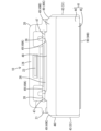
- FIG. 8 is a side cross-sectional view showing a state in which the body portion is arranged behind the lead portions and between the reinforcing plate and the board pressing portion in a state in which movement is restricted in the connector of the second embodiment.
- FIG. 9 is a rear view of the connector of the second embodiment.
- fixing members 30 are press-fitted onto the left and right outer surfaces of the housing body 21.
- the fixing members 30 are made of a metal plate and are fixed by soldering while penetrating the circuit board 90.
- the housing 20 is fixed to the circuit board 90 via the fixing members 30.
- the housing 20 has a lock arm 23 that protrudes from the top surface of the housing body 21.
- the lock arm 23 is elastically deformable and engages the mating connector, maintaining the connector 10 and the mating connector in a mated state.
- the housing 20 also has a bridge portion 24 that is connected to the rear end of the lock arm 23. The bridge portion 24 is bridged above the rear end of the housing body 21 so as to extend in the left-right direction.
- the housing 20 has side walls 26 that protrude rearward from both the left and right ends of the rear surface (drawer surface 25) of the housing main body 21.
- the upper surface of the front end of each side wall 26 is connected to the bridge portion 24.
- each side wall 26 is installed on the surface of the circuit board 90.
- Each side wall 26 laterally covers and protects the lead portions 82 (described later) of the terminal fittings 80 located at both the left and right ends.
- a locking portion 27 is formed on the outer side surface of the front end of each side wall 26.
- the locking portion 27 has a groove shape that extends in the vertical direction on the outer side surface of the side wall 26, and can be locked to a locking portion 52 (described later) of the cover member 40.
- the housing 20 has a eaves portion 28 that protrudes rearward from the upper end of the pull-out surface 25 of the housing body 21.
- the eaves portion 28 is a horizontal plate extending in the left-right direction. Both left and right ends of the eaves portion 28 are integrally connected to each side wall 26, and are longer than the left and right intermediate portions of the eaves portion 28 in the front-rear direction, and are formed over the entire length of each side wall 26.
- a step 29 is formed on the underside of the housing body 21.
- the underside of the front end of the housing body 21 is positioned one step lower than the underside of the rear part of the housing body 21 (the part behind the front end) via the step 29.
- the circuit board 90 is front-stopped by the step 29 to determine the position of its front end.
- Terminal metal fitting 80 The terminal fittings 80 are integrally formed by bending a conductive metal plate, etc. As shown in Figures 4 and 5, the terminal fittings 80 have a cylindrical main body portion 81 and a strip-shaped lead portion 82 extending rearward from the main body portion 81. The main body portion 81 is accommodated in each cavity 22 inside the housing 20. A tab of a mating terminal fitting (not shown) is inserted into the main body portion 81 for connection.
- the lead portion 82 is pulled out rearward from the pull-out surface 25 of the housing 20. As shown in FIG. 5, the lead portion 82 has a portion that extends downward at a position rearward of the housing 20. The rear lower end of the lead portion 82 forms a board connection portion 83 that is disposed along the surface of the circuit board 90. The board connection portion 83 is connected by soldering to a conductive portion 92 (pad) formed on the circuit board 90.
- the board connection portions 83 of each terminal fitting 80 are arranged in a zigzag pattern in the front-to-back direction on the circuit board 90 while being aligned in multiple rows in the left-to-right direction.
- the circuit board 90 is composed of a hard reinforcing plate 93 and a flexible resin film-like board body 94 that is laminated and supported by the reinforcing plate 93.
- the conductive portion 92 is formed on the surface (mounting surface) of the board body 94.
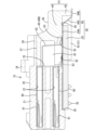
- the lead portion 82 drawn out from the upper cavity 22 is formed to be longer than the lead portion 82 drawn out from the lower cavity 22. As shown in FIG. 3, the lead portion 82 drawn out from the upper cavity 22 has a wide portion 84 located at the top and a narrow portion 85 located at the bottom, which is narrower than the wide portion 84. The lead portion 82 drawn out from the lower cavity 22 is arranged side by side with the narrow portion 85 in the left-right direction to narrow the pitch between adjacent terminal fittings 80. The lead portion 82 drawn out from the lower cavity 22 has a width dimension equivalent to that of the narrow portion 85.
- the cover member 40 is made of synthetic resin and is attached to the housing 20 from the rear. As shown in Fig. 7, the cover member 40 has a board pressing portion 41 arranged at the rear, a covering portion 46 and a plurality of insulating portions 42 arranged at the left and right intermediate portions (excluding the left and right ends) of the front, and side portions 43 arranged at the left and right ends of the front.
- the board holder 41 is arranged so as to be in contact with the board body 94 of the circuit board 90, and holds the board body 94 between itself and the reinforcing plate 93 of the circuit board 90 so as not to move.
- the board holder 41 is arranged in contact with or in close proximity to the board body 94 of the circuit board 90, and when an external force is applied to the circuit board 90, it comes into contact with the board body 94 to restrict the movement of the board body 94.
- the board holder 41 is arranged behind each lead portion 82 pulled out from the pull-out surface 25 of the housing 20, so as to cover each lead portion 82 from behind.
- the board pressing portion 41 has a pressing body 44 that is long in the left-right direction and thick in the up-down direction.
- the underside of the pressing body 44 is arranged horizontally along the left-right direction and the front-rear direction.
- the board pressing portion 41 also has a pressing end 45 that protrudes downward from the rear end of the pressing body 44.
- the pressing end 45 is formed over the entire length of the pressing body 44 in the left-right direction.
- the underside of the pressing end 45 is arranged lower than the underside of the pressing body 44.
- the underside of the pressing end 45 is arranged along the left-right direction and is continuous with the underside of each side portion 43 at the same height.
- the board body 94 of the circuit board 90 has a first board body 94A that is supported by stacking on the reinforcing plate 93, and a second board body 94B that is arranged behind the reinforcing plate 93 and not supported by the reinforcing plate 93.
- the first board body 94A includes a conductive portion 92 and is sandwiched between the reinforcing plate 93 and the pressing body 44 in the vertical direction.
- the second board body 94B is stretched in the front-rear direction while being pressed from above by the pressing end portion 45.
- the board body 94 has a third board body 94C that is bent from the upper corner portion 95 at the rear end of the reinforcing plate 93 and inclined downward from the first board body 94A to the second board body 94B.
- the third board body 94C maintains an inclined (bent) state in the front-rear direction between the upper corner portion 95 of the reinforcing plate 93 and the pressing end portion 45.
- the board body 94 and the reinforcing plate 93 are formed with a width dimension that corresponds to the left-right width dimension of the housing 20.
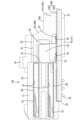
- the covering portion 46 is a plate that is long in the left-right direction and forms the upper wall of the front part of the cover member 40. As shown in FIG. 3, the covering portion 46 is arranged so as to cover each lead portion 82 collectively from above. As shown in FIG. 7, the upper surface of the covering portion 46 has a high surface 47 that extends from the front end to both left and right ends, a low surface 48 that is positioned lower than the high surface 47 in the middle left and right part of the rear part, and a first inclined surface 49A (inclined surface 49) that slopes downward from the high surface 47 to the low surface 48.
- a first inclined surface 49A inclined surface 49
- the high surface 47 of the cover portion 46 is gate-shaped in plan view and is arranged along the left-right and front-rear directions. As shown in Figures 3 and 5, the high surface 47 is arranged to infiltrate into the underside of the eaves portion 28.
- the first slope 49A is arranged to slope downward as it moves away from the eaves portion 28.
- a second slope 49B (slope 49) is also formed on the upper surface of the board holding portion 41, which slopes downward as it moves rearward from the eaves portion 28.
- the second slope 49B is connected to the rear ends of the first slope 49A and the low surface 48, and is formed over the entire length of the board holding portion 41 in the left-right direction.
- each insulating portion 42 is arranged between all pairs of adjacent lead portions 82 in the left-right direction.
- Each insulating portion 42 has a first insulating portion 42A that protrudes downward from the cover portion 46, and a second insulating portion 42B that is connected to the lower end of the first insulating portion 42A.
- Each first insulating portion 42A is plate-shaped and arranged vertically in the up-down and front-to-rear directions.
- Each first insulating portion 42A is arranged on both the left and right sides of the corresponding lead portion 82 pulled out from the upper cavity 22 so as to cover the lead portion 82 from the side.
- Each second insulating portion 42B has a portion that protrudes from one side of the plate surface of each first insulating portion 42A (left side in FIG. 3) and a portion that extends downward from the end of that portion on one side.
- the first insulating portion 42A and the second insulating portion 42B are formed continuously in a gate type when viewed from the front, and the corresponding lead portion 82 drawn from the lower cavity 22 is accommodated and arranged in the internal space that is open downward.
- the wide portion 84 of the corresponding lead portion 82 drawn from the upper cavity 22 is accommodated and arranged in the space between adjacent first insulating portions 42A and above the second insulating portion 42B.
- the narrow portion 85 of the corresponding lead portion 82 drawn from the upper cavity 22 is accommodated and arranged in the space between adjacent first insulating portions 42A and second insulating portions 42B.
- each side portion 43 is positioned to protrude forward from both the left and right ends of the board holding portion 41.
- Each side portion 43 has a plate-shaped side plate portion 51 that is positioned along the up-down and front-to-back directions.
- Each side plate portion 51 is elastically deformable in the left-right direction with the connection portion with the board holding portion 41 as a fulcrum.
- each side plate portion 51 is positioned to cover each side wall 26 from the side.
- each side portion 43 has a locking portion 52 protruding from the inner surface of each side plate portion 51 (the surface where each side plate portion 51 faces in the left-right direction).
- the locking portion 52 is shaped like a long claw in the vertical direction and is connected to the upper front end of the inner surface of each side plate portion 51.
- each locking portion 52 fits into the corresponding locked portion 27, thereby holding the cover member 40 in a state where it is prevented from coming off the housing 20.
- a third inclined surface 49C (inclined surface 49) that slopes downward on both left and right ends is formed on the upper surface of each side portion 43.
- the cover member 40 is placed on the housing 20 from the rear so as to cover each lead portion 82 drawn out from the drawing surface 25 of the housing 20.
- the locking portions 52 of each side portion 43 are locked to the corresponding locked portions 27 of the housing 20, and the cover member 40 is held on the housing 20.
- the high surface 47 of the cover portion 46 is arranged to be in contact with and face the lower surface of the eaves portion 28.
- Each insulating portion 42 is arranged between adjacent lead portions 82 in the left-right direction.
- the lead portions 82 drawn out from the upper cavity 22 are arranged between adjacent first insulating portions 42A in the left-right direction, except for the lead portions 82 arranged at both left and right ends.
- the lead portions 82 drawn out from the upper cavity 22 and arranged at both left and right ends are arranged between adjacent first insulating portions 42A in the left-right direction and the side walls 26.
- the lead portions 82 drawn out from the lower cavity 22 are disposed in an internal space formed between the first insulating portion 42A and the second insulating portion 42B. As a result, all pairs of lead portions 82 adjacent in the left-right direction are shielded from each other, making it possible to prevent leakage between the terminal fittings 80.
Landscapes
- Coupling Device And Connection With Printed Circuit (AREA)
- Connector Housings Or Holding Contact Members (AREA)
Priority Applications (1)
| Application Number | Priority Date | Filing Date | Title |
|---|---|---|---|
| CN202480063542.5A CN121970216A (zh) | 2023-10-13 | 2024-10-03 | 连接器 |
Applications Claiming Priority (2)
| Application Number | Priority Date | Filing Date | Title |
|---|---|---|---|
| JP2023-177346 | 2023-10-13 | ||
| JP2023177346A JP2025067395A (ja) | 2023-10-13 | 2023-10-13 | コネクタ |
Publications (1)
| Publication Number | Publication Date |
|---|---|
| WO2025079498A1 true WO2025079498A1 (ja) | 2025-04-17 |
Family
ID=95395344
Family Applications (1)
| Application Number | Title | Priority Date | Filing Date |
|---|---|---|---|
| PCT/JP2024/035468 Pending WO2025079498A1 (ja) | 2023-10-13 | 2024-10-03 | コネクタ |
Country Status (3)
| Country | Link |
|---|---|
| JP (1) | JP2025067395A (https=) |
| CN (1) | CN121970216A (https=) |
| WO (1) | WO2025079498A1 (https=) |
Citations (5)
| Publication number | Priority date | Publication date | Assignee | Title |
|---|---|---|---|---|
| JPH08288019A (ja) * | 1994-07-22 | 1996-11-01 | Connector Syst Technol Nv | 少なくとも1の同軸あるいは2軸端子を有する選択的に金属化されたコネクタ |
| JPH09204952A (ja) * | 1996-01-29 | 1997-08-05 | Sumitomo Wiring Syst Ltd | コネクタハウジング |
| JPH10199640A (ja) * | 1997-01-10 | 1998-07-31 | Fujitsu Takamizawa Component Kk | コネクタとその製造方法 |
| JP2014093379A (ja) * | 2012-11-01 | 2014-05-19 | Denso Corp | 電子装置用ケース |
| JP2019169345A (ja) * | 2018-03-23 | 2019-10-03 | 第一精工株式会社 | 防塵カバー、及びコネクタ |
-
2023
- 2023-10-13 JP JP2023177346A patent/JP2025067395A/ja active Pending
-
2024
- 2024-10-03 CN CN202480063542.5A patent/CN121970216A/zh active Pending
- 2024-10-03 WO PCT/JP2024/035468 patent/WO2025079498A1/ja active Pending
Patent Citations (5)
| Publication number | Priority date | Publication date | Assignee | Title |
|---|---|---|---|---|
| JPH08288019A (ja) * | 1994-07-22 | 1996-11-01 | Connector Syst Technol Nv | 少なくとも1の同軸あるいは2軸端子を有する選択的に金属化されたコネクタ |
| JPH09204952A (ja) * | 1996-01-29 | 1997-08-05 | Sumitomo Wiring Syst Ltd | コネクタハウジング |
| JPH10199640A (ja) * | 1997-01-10 | 1998-07-31 | Fujitsu Takamizawa Component Kk | コネクタとその製造方法 |
| JP2014093379A (ja) * | 2012-11-01 | 2014-05-19 | Denso Corp | 電子装置用ケース |
| JP2019169345A (ja) * | 2018-03-23 | 2019-10-03 | 第一精工株式会社 | 防塵カバー、及びコネクタ |
Also Published As
| Publication number | Publication date |
|---|---|
| JP2025067395A (ja) | 2025-04-24 |
| CN121970216A (zh) | 2026-05-01 |
Similar Documents
| Publication | Publication Date | Title |
|---|---|---|
| US7458822B2 (en) | Electrical connector and combination connector having the same | |
| CN101375471B (zh) | 连接器 | |
| CN100511868C (zh) | 电路基板用电连接器 | |
| US6676433B1 (en) | Connector | |
| US10804652B2 (en) | Electrical connector | |
| KR20080101871A (ko) | 커넥터 | |
| JP7419146B2 (ja) | コネクタ及び電子機器 | |
| US20080026609A1 (en) | Low profile connector | |
| KR20060093270A (ko) | 케이블 커넥터 | |
| JP5315912B2 (ja) | 多連装電気コネクタ | |
| US20080139007A1 (en) | Electrical connector | |
| KR100815708B1 (ko) | Emi특성이 용이하게 개선된 작은 사이즈의 전기 커넥터 | |
| US9350120B2 (en) | Plug connector and method of manufacturing the same | |
| WO2025079498A1 (ja) | コネクタ | |
| WO2025079500A1 (ja) | コネクタ | |
| CN114270632B (zh) | 连接器和电子设备 | |
| US7309254B2 (en) | Connector which can be increased in holding strength with respect to a substrate | |
| JP2019114474A (ja) | 電気コネクタ | |
| JP7783000B2 (ja) | 基板実装型のコネクタ、及び、コネクタ付き基板 | |
| JP2008140555A (ja) | コネクタ装置 | |
| KR102951948B1 (ko) | 커넥터 | |
| JP2021182486A (ja) | コネクタ、及び、コネクタユニット | |
| WO2025070093A1 (ja) | コネクタ | |
| TWI661615B (zh) | 車用連接器組合 | |
| JP2025137379A (ja) | コネクタ |
Legal Events
| Date | Code | Title | Description |
|---|---|---|---|
| 121 | Ep: the epo has been informed by wipo that ep was designated in this application |
Ref document number: 24875647 Country of ref document: EP Kind code of ref document: A1 |