WO2025069986A1 - 積層体、仮想現実表示装置、積層体の製造方法 - Google Patents
積層体、仮想現実表示装置、積層体の製造方法 Download PDFInfo
- Publication number
- WO2025069986A1 WO2025069986A1 PCT/JP2024/031969 JP2024031969W WO2025069986A1 WO 2025069986 A1 WO2025069986 A1 WO 2025069986A1 JP 2024031969 W JP2024031969 W JP 2024031969W WO 2025069986 A1 WO2025069986 A1 WO 2025069986A1
- Authority
- WO
- WIPO (PCT)
- Prior art keywords
- laminate
- layer
- anisotropic layer
- film
- liquid crystal
- Prior art date
- Legal status (The legal status is an assumption and is not a legal conclusion. Google has not performed a legal analysis and makes no representation as to the accuracy of the status listed.)
- Ceased
Links
Images





Classifications
-
- G—PHYSICS
- G02—OPTICS
- G02B—OPTICAL ELEMENTS, SYSTEMS OR APPARATUS
- G02B5/00—Optical elements other than lenses
- G02B5/30—Polarising elements
- G02B5/3016—Polarising elements involving passive liquid crystal elements
-
- B—PERFORMING OPERATIONS; TRANSPORTING
- B32—LAYERED PRODUCTS
- B32B—LAYERED PRODUCTS, i.e. PRODUCTS BUILT-UP OF STRATA OF FLAT OR NON-FLAT, e.g. CELLULAR OR HONEYCOMB, FORM
- B32B1/00—Layered products having a non-planar shape
-
- B—PERFORMING OPERATIONS; TRANSPORTING
- B32—LAYERED PRODUCTS
- B32B—LAYERED PRODUCTS, i.e. PRODUCTS BUILT-UP OF STRATA OF FLAT OR NON-FLAT, e.g. CELLULAR OR HONEYCOMB, FORM
- B32B7/00—Layered products characterised by the relation between layers; Layered products characterised by the relative orientation of features between layers, or by the relative values of a measurable parameter between layers, i.e. products comprising layers having different physical, chemical or physicochemical properties; Layered products characterised by the interconnection of layers
- B32B7/02—Physical, chemical or physicochemical properties
- B32B7/023—Optical properties
-
- B—PERFORMING OPERATIONS; TRANSPORTING
- B32—LAYERED PRODUCTS
- B32B—LAYERED PRODUCTS, i.e. PRODUCTS BUILT-UP OF STRATA OF FLAT OR NON-FLAT, e.g. CELLULAR OR HONEYCOMB, FORM
- B32B7/00—Layered products characterised by the relation between layers; Layered products characterised by the relative orientation of features between layers, or by the relative values of a measurable parameter between layers, i.e. products comprising layers having different physical, chemical or physicochemical properties; Layered products characterised by the interconnection of layers
- B32B7/04—Interconnection of layers
- B32B7/12—Interconnection of layers using interposed adhesives or interposed materials with bonding properties
-
- B—PERFORMING OPERATIONS; TRANSPORTING
- B32—LAYERED PRODUCTS
- B32B—LAYERED PRODUCTS, i.e. PRODUCTS BUILT-UP OF STRATA OF FLAT OR NON-FLAT, e.g. CELLULAR OR HONEYCOMB, FORM
- B32B9/00—Layered products comprising a layer of a particular substance not covered by groups B32B11/00 - B32B29/00
- B32B9/04—Layered products comprising a layer of a particular substance not covered by groups B32B11/00 - B32B29/00 comprising such particular substance as the main or only constituent of a layer, which is next to another layer of the same or of a different material
- B32B9/045—Layered products comprising a layer of a particular substance not covered by groups B32B11/00 - B32B29/00 comprising such particular substance as the main or only constituent of a layer, which is next to another layer of the same or of a different material of synthetic resin
-
- G—PHYSICS
- G02—OPTICS
- G02B—OPTICAL ELEMENTS, SYSTEMS OR APPARATUS
- G02B27/00—Optical systems or apparatus not provided for by any of the groups G02B1/00 - G02B26/00, G02B30/00
- G02B27/10—Beam splitting or combining systems
- G02B27/14—Beam splitting or combining systems operating by reflection only
- G02B27/144—Beam splitting or combining systems operating by reflection only using partially transparent surfaces without spectral selectivity
-
- G—PHYSICS
- G02—OPTICS
- G02B—OPTICAL ELEMENTS, SYSTEMS OR APPARATUS
- G02B5/00—Optical elements other than lenses
- G02B5/30—Polarising elements
-
- B—PERFORMING OPERATIONS; TRANSPORTING
- B32—LAYERED PRODUCTS
- B32B—LAYERED PRODUCTS, i.e. PRODUCTS BUILT-UP OF STRATA OF FLAT OR NON-FLAT, e.g. CELLULAR OR HONEYCOMB, FORM
- B32B2305/00—Condition, form or state of the layers or laminate
- B32B2305/55—Liquid crystals
-
- B—PERFORMING OPERATIONS; TRANSPORTING
- B32—LAYERED PRODUCTS
- B32B—LAYERED PRODUCTS, i.e. PRODUCTS BUILT-UP OF STRATA OF FLAT OR NON-FLAT, e.g. CELLULAR OR HONEYCOMB, FORM
- B32B2307/00—Properties of the layers or laminate
- B32B2307/40—Properties of the layers or laminate having particular optical properties
- B32B2307/42—Polarizing, birefringent, filtering
-
- B—PERFORMING OPERATIONS; TRANSPORTING
- B32—LAYERED PRODUCTS
- B32B—LAYERED PRODUCTS, i.e. PRODUCTS BUILT-UP OF STRATA OF FLAT OR NON-FLAT, e.g. CELLULAR OR HONEYCOMB, FORM
- B32B2457/00—Electrical equipment
- B32B2457/20—Displays, e.g. liquid crystal displays, plasma displays
- B32B2457/202—LCD, i.e. liquid crystal displays
Definitions
- the present invention relates to a laminate, a virtual reality display device, and a method for manufacturing the laminate.
- a virtual reality display device is a display device that allows users to feel as if they are immersed in a virtual world by wearing a dedicated headset on their head and viewing images displayed through lenses.
- a configuration known as a pancake lens has been proposed, which has an image display device, a reflective polarizer, a half mirror, and a phase difference layer, and reduces the overall thickness of the headset by directing the light emitted from the image display device back and forth between the reflective polarizer and the half mirror.
- an absorptive polarizer is also used in the pancake lens described above.
- Patent Document 1 discloses a polarizer that contains a dichroic dye and has a curved portion.
- the inventors produced a virtual reality display device using a polarizing plate having a curved portion as disclosed in Patent Document 1 as an absorptive polarizer, and when they evaluated its characteristics, they found that the color of the displayed image changed over time.
- the light absorption anisotropic layer is also required to have excellent adhesion.
- an object of the present invention is to provide a laminate that can realize a virtual reality display device in which changes in color of a displayed image over time are suppressed and that also has excellent adhesion of a light absorbing anisotropic layer.
- Another object of the present invention is to provide a virtual reality display device and a method for manufacturing a laminate.
- a substrate an adhesive or bonding layer; A laminate having, in this order, a light absorbing anisotropic layer, the light absorption anisotropic layer contains a liquid crystal compound having smectic liquid crystallinity,
- the laminate has a curved surface portion, A laminate, in which the optically absorptive anisotropic layer in the curved surface portion satisfies the requirement X described below.
- the composition contains a thiol compound.
- the alignment film is a layer formed from a composition containing a compound having an active hydrogen reactive group.
- a virtual reality display device comprising the laminate according to any one of (1) to (16).
- the present invention it is possible to realize a virtual reality display device in which the change in color tone of a displayed image over time is suppressed, and it is also possible to provide a laminate having excellent adhesion of an optically absorptive anisotropic layer.
- the present invention also provides a virtual reality display device and a method for manufacturing a laminate.
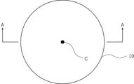
- FIG. 1 is a top view of an example of the laminate of the present invention.
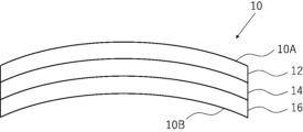
- FIG. 2 is a cross-sectional view taken along line AA in FIG.
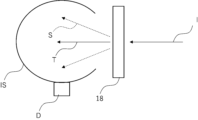
- FIG. 3 is a diagram for explaining a measurement method using an integrating sphere.
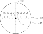
- FIG. 4 is a diagram for explaining the measurement positions of the film thickness of the optically absorptive anisotropic layer.
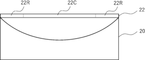
- FIG. 5 is a diagram for explaining the procedure for forming a film using a mold having a concave forming surface.
- FIG. 6 is a diagram for explaining the procedure for forming a film using a mold having a concave forming surface.
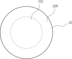
- FIG. 7 is a top view of the film used for molding.
- FIG. 8 is a diagram for explaining the procedure for forming a film using a mold having a convex forming surface.
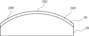
- FIG. 9 is a diagram for explaining the procedure for forming a film using a mold having a convex forming surface.
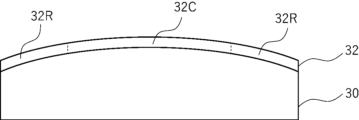
- FIG. 10 is a diagram for explaining the method 1.
- FIG. FIG. 11 is a diagram for explaining the method 1.
- FIG. FIG. 12 is a diagram for explaining the method 1.
- FIG. FIG. 13 is a diagram for explaining the method 2.
- FIG. FIG. 14 is a top view of the planar precursor film used in method 2.
- FIG. 15 is a cross-sectional view showing an example of the laminate of the present invention.
- FIG. 16 is a cross-sectional view showing another example of the laminate of the present invention.
- FIG. 17 is a diagram showing an example of the virtual reality display device of the present invention.
- absorption axis refers to the polarization direction in which the absorbance is maximum in the plane when linearly polarized light is incident.
- reflection axis refers to the polarization direction in which the reflectance is maximum in the plane when linearly polarized light is incident.
- transmission axis refers to the direction perpendicular to the absorption axis or reflection axis in the plane.
- slow axis refers to the direction in which the refractive index is maximum in the plane.
- Re( ⁇ ) and Rth( ⁇ ) respectively represent the in-plane retardation and the thickness retardation at a wavelength ⁇ .
- the wavelength ⁇ is 550 nm.
- Re( ⁇ ) and Rth( ⁇ ) are values measured at a wavelength ⁇ using an AxoScan (manufactured by Axometrics).
- AxoScan manufactured by Axometrics.
- Re( ⁇ ) R0( ⁇ )
- NAR-4T Abbe refractometer
- the measurement can be performed using a multi-wavelength Abbe refractometer DR-M2 (manufactured by Atago Co., Ltd.) in combination with an interference filter.
- values in the Polymer Handbook JOHN WILEY & SONS, INC.
- catalogs of various optical films can be used.
- Examples of average refractive index values of major optical films are as follows: cellulose acylate (1.48), cycloolefin polymer (1.52), polycarbonate (1.59), polymethyl methacrylate (1.49), and polystyrene (1.59).
- the A plate and the C plate are defined as follows. There are two types of A plates, positive A plates and negative A plates, and when the refractive index in the slow axis direction (the direction in which the refractive index in the plane is maximum) in the film plane is nx, the refractive index in the direction perpendicular to the slow axis in the plane is ny, and the refractive index in the thickness direction is nz, the positive A plate satisfies the relationship of formula (A1), and the negative A plate satisfies the relationship of formula (A2). Note that the positive A plate has a positive Rth value, and the negative A plate has a negative Rth value.
- Formula (A1) nx>ny ⁇ nz
- Formula (A2) ny ⁇ nx ⁇ nz
- ⁇ includes not only the case where the two are completely identical, but also the case where the two are substantially identical.
- “ny ⁇ nz” includes the case where (ny-nz) ⁇ d (where d is the thickness of the film) is -10 to 10 nm, preferably -5 to 5 nm
- “nx ⁇ nz” includes the case where (nx-nz) ⁇ d is -10 to 10 nm, preferably -5 to 5 nm.
- a feature of the laminate of the present invention is that the optically absorptive anisotropic layer in the curved surface portion satisfies the requirement X described below.
- the present inventors have investigated the cause of the change in color of a displayed image over time when a virtual reality display device is produced using a polarizing plate (corresponding to a light-absorption anisotropic layer) having a curved surface manufactured by a conventional technique such as Patent Document 1 as an absorptive polarizer. As a result, they have found that the cause is the occurrence of molecular density variations in the polarizing plate when the polarizing plate is molded.
- Requirement X specifies that the difference between the degree of polarization measured without using an integrating sphere and the degree of polarization measured with an integrating sphere must be within a predetermined range, and the difference is small when the molecular density in the optically absorptive anisotropic layer is small.
- the inventors have found that the above-mentioned problems can be solved by an optically absorptive anisotropic layer in which the difference as defined by requirement X is within the predetermined range.
- the optically absorptive anisotropic layer since a pressure-sensitive adhesive layer or a bonding layer is disposed between the substrate and the optically absorptive anisotropic layer, the optically absorptive anisotropic layer also has excellent adhesion (adhesion of the optically absorptive anisotropic layer to the substrate).
- FIG. 1 shows an example of the laminate of the present invention.
- Fig. 1 is a top view of the laminate
- Fig. 2 is a cross-sectional view taken along line AA in Fig. 1.
- Line AA is a line passing through center C of laminate 10, which is circular when viewed in plan.
- the laminate 10 has a substrate 12, an adhesive layer 14, and an optically absorptive anisotropic layer 16 in this order.
- the laminate 10 has a curved shape. More specifically, as shown in Figure 2, the laminate 10 has a shape that is curved convexly toward the upper side of the paper (convex shape). In other words, the laminate 10 has a convex shape that protrudes on one surface side.
- the laminate 10 has a concave shape with the other surface side recessed.
- the entire laminate 10 corresponds to the curved surface portion.
- the laminate 10 has two opposing surfaces, a first surface 10A and a second surface 10B.
- the first surface 10A is a curved surface that is convex toward the upper side of the paper
- the second surface 10B is a curved surface that is convex toward the upper side of the paper.
- the curved surface shape of the laminate 10 shown in FIGS. 1 and 2 is a paraboloid of revolution, it may be a spherical shape or a spheroid of revolution.
- an adhesive layer is used in FIGS. 1 and 2
- an adhesive layer may be used.
- the shape of the laminate 10 is circular.
- the center C of the laminate 10 is the intersection point between the axis of the spheroid shape and the laminate 10, and corresponds to the position where the laminate 10 intersects with the normal to the center of the exit surface of the image display panel when the laminate 10 is incorporated into the virtual reality display device described below.
- the laminate 10 is disposed so as to be convex toward the image display panel side.
- the curved surface of the laminate is circular when viewed in a plane, but the present invention is not limited to this, and the curved surface of the laminate may be elliptical or have another shape when viewed in a plane.
- the configuration of the curved surface portion of the laminate is not limited to the configurations shown in FIGS.
- the curved shape of the curved shape portion means a shape having a curvature exceeding 0, and includes a developable curved shape and a three-dimensional curved shape.
- a developable surface is a surface that can be developed into a plane without stretching or contracting any part of the surface. Examples of the curved shape that is a developable surface include surfaces that correspond to the peripheral surface of a cylinder, an elliptical cylinder, a cone, and an elliptical cone, and may be a convex curved surface or a concave curved surface.
- a three-dimensional curved surface means a curved surface that is not established by deformation of a plane, that is, a curved surface that is not a developable surface, and examples of the three-dimensional curved surface include surfaces that correspond to a spherical surface and a spheroidal surface, and surfaces that correspond to a curved surface whose cross section is a parabola or hyperbola (for example, a paraboloid of revolution), and may be a convex curved surface or a concave curved surface.
- the curved surface shape is preferably lenticular.
- lenticular curved surfaces include spherical and ellipsoidal shapes, and may be either convex or concave lenticular.
- the curved surface portion of the laminate is preferably a spherical surface, a spheroidal surface, or a paraboloidal surface.
- the curved surface portion is a spherical surface, a spheroidal surface, or a paraboloidal surface.
- the optically absorptive anisotropic layer in the curved surface portion of the laminate satisfies requirement X.
- Requirement X When the degree of polarization of an optically absorptive anisotropic layer measured without using an integrating sphere is defined as P1, and the degree of polarization of an optically absorptive anisotropic layer measured using an integrating sphere is defined as P2, the degree of polarization P1 and the degree of polarization P2 satisfy the relationship of formula (1).
- FIG. 3 shows a method for measuring the degree of polarization using a detector D having an integrating sphere IS.
- the degree of polarization P2 calculated by the formula described later is likely to be small.
- the reason why the degree of polarization is likely to be small is that the transmittance in the absorption axis direction in formula (2) described later is large.
- the scattered light S is not detected by the detector as shown in Fig. 3.
- the transmittance in the absorption axis direction in formula (2) described later tends to be small, and as a result, the degree of polarization P1 tends to be large.
- the likelihood of scattered light S occurring varies depending on the density of the molecular density, and the more density interfaces there are in the light absorption anisotropic layer, the more likely the scattered light S is to occur, and in such a case, the polarization degree P2 tends to be smaller.
- the difference between the polarization degree P1 and the polarization degree P2 becomes larger.
- the difference between the polarization degree P1 and the polarization degree P2 represents the degree of abundance of density interfaces in the sample, and the smaller this value is, the fewer density interfaces there are.
- the laminate of the present invention satisfies requirement Y in that the change over time in color tone of a displayed image is further suppressed in a virtual reality display device to which the laminate of the present invention is applied.
- Requirement Y The polarization degree P1 and the polarization degree P2 satisfy the relationship of formula (2). Equation (2) Polarization degree P1 ⁇ Polarization degree P2 ⁇ 0.15%
- the lower limit of the difference between the polarization degree P1 and the polarization degree P2 (polarization degree P1-polarization degree P2) is not particularly limited, but may be 0%.
- the magnitude of the polarization degree P1 is not particularly limited as long as it satisfies the above-mentioned requirement X, but 70 to 100% is preferable, 80 to 99.9% is more preferable, and 95.0 to 99.9% is even more preferable.
- the degree of polarization P1 is calculated by irradiating light from the normal direction of the surface of the optically absorptive anisotropic layer without using an integrating sphere. More specifically, linearly polarized light parallel to the transmission axis of the optically absorptive anisotropic layer is irradiated from the normal direction of the surface of the optically absorptive anisotropic layer to measure the transmittance T1, and linearly polarized light parallel to the absorption axis of the optically absorptive anisotropic layer is irradiated to measure the transmittance T2, and the degree of polarization P1 is calculated by the following formula.
- T1 transmittance for polarized light in the transmission axis direction of the light-absorptive anisotropic layer
- T2 transmittance for polarized light in the absorption axis direction of the light-absorptive anisotropic layer
- the average transmittance is calculated by weighting the transmittance values obtained by the above measurement every 5 nm between 380 and 780 nm using the Y value of the XYZ color matching function (color matching function of the CIE 1931 standard observer) standardized by the CIE (Commission Internationale de Illumination). That is, a calculated value A, which is the product of the transmittance value measured every 5 nm between 380 and 780 nm and the Y value corresponding to the transmittance measurement wavelength, is calculated for each measurement wavelength, and the calculated values A obtained at each measurement wavelength are summed to calculate a total value B.
- a calculated value A which is the product of the transmittance value measured every 5 nm between 380 and 780 nm and the Y value corresponding to the transmittance measurement wavelength
- the obtained total value B is further divided by the total value C of the Y values used above (total value B/total value C), thereby calculating the transmittance. Furthermore, when calculating the degree of polarization P2, a detector having an integrating sphere is used, and the calculation is performed in the same manner as in the calculation of the degree of polarization P1.
- the distance between the detector having the integrating sphere and the optically absorptive anisotropic layer serving as the measurement sample is preferably 5 mm.
- the polarization degree P1 and the polarization degree P2 are calculated by eliminating the influence of the other members on the polarization degree. For example, the polarization degree P1 and the polarization degree P2 may be calculated after confirming in advance that the other members are not affected by irradiating light.
- the sample for measuring the polarization degree P1 and the polarization degree P2 may be prepared by cutting out a part of the curved portion in the laminate.
- a sample of the optically absorptive anisotropic layer having a shape similar to that of the curved portion in the laminate may be prepared separately and used as the measurement sample.
- the radius of curvature of the curved surface of the laminate is not particularly limited, but is preferably 20 to 80 mm, more preferably 30 to 80 mm, and even more preferably 35 to 60 mm, in that the occurrence of ghosts is further suppressed when the laminate is applied to a virtual reality display device.
- the radius of curvature of the curved portion may be constant or may vary at any position on the curved portion, and it is preferable that the radius of curvature at any position is within the above range.
- the shape of the curved portion corresponds to a spherical shape.
- the size of the curved shape portion of the laminate when viewed in plan from the rotation axis direction of these shapes is not particularly limited, and the circle equivalent diameter of the curved shape portion is preferably 30 to 80 mm, and more preferably 40 to 60 mm.
- the equivalent circle diameter is the diameter of a perfect circle having the same projected area as the projected area of the curved surface portion during observation.
- the film thickness of the curved surface portion is not particularly limited, but in terms of obtaining a better effect of the present invention, the film thickness is preferably 0.5 to 5.0 ⁇ m, and more preferably 1.0 to 3.0 ⁇ m.
- the above-mentioned film thickness means an average film thickness obtained when calculating the in-plane variation in the film thickness of the light absorptive anisotropic layer on the curved surface portion.
- the in-plane variation in the thickness of the optically absorptive anisotropic layer in the curved surface portion of the laminate of the present invention is not particularly limited, but is preferably 7% or less, more preferably 4% or less, in order to further suppress the occurrence of ghosts when the laminate is applied to a virtual reality display device.
- the lower limit is not particularly limited, and may be 0%, and is often 0.1% or more.
- the in-plane variation in thickness of the light absorptive anisotropic layer in the curved surface portion can be measured by the following method.
- the laminate is cut with a microtome to expose a cross section, which is then observed with a scanning electron microscope (SEM) at an appropriate magnification (20,000 to 50,000 times) to determine the film thickness of the optically absorptive anisotropic layer in the curved portion.
- SEM scanning electron microscope
- the measurement sample may be subjected to appropriate treatment such as carbon deposition, etching, etc.
- the accelerating voltage is preferably optimized within the range of 1 to 10 kV.
- the position in the curved portion where the film thickness of the optically absorptive anisotropic layer is measured is determined by the following method:
- the laminate 10 shown in Figures 1 and 2 will be described as an example.
- the laminate is viewed from above in the normal direction of the emission surface of the image display panel, and the intersection point of the laminate viewed from above, which passes through the center of the emission surface and extends in the normal direction, is defined as the center of the curved surface portion.
- the center C of the laminate 10 corresponds to the center of the curved surface portion.
- a straight line passing through the center and extending in one in-plane direction is defined as a first straight line
- a straight line extending in the in-plane direction perpendicular to the first straight line is defined as a second straight line.
- a straight line passing through the center C and extending in the left-right direction of the paper is defined as a first straight line SL1
- a straight line extending perpendicular to the straight line SL1 is defined as a second straight line SL2.
- the lines extending in the left-right direction and the up-down direction of the paper are defined as the first straight line and the second straight line, but this is not limited to the above, and any straight line extending in one in-plane direction may be adopted as the first straight line.
- the first straight line and the second straight line located within the area of the curved surface shape portion (within the area of the projected image) in plan view are each divided into 10 parts. As shown in FIG. 4, the first straight line SL1 and the second straight line SL2 shown by dashed lines are divided into 10 parts of equal length.
- the first straight line SL1 is divided into 10 parts to obtain 8 division lines (D1 to D8) excluding the division lines located at both ends, and the position of any one point on each division line is selected, and the film thickness at the position of the optically anisotropic layer corresponding to that position is calculated.
- the position of the optically anisotropic layer corresponding to any position on the division line corresponds to the intersection point between the optically anisotropic layer and an axis extending in the normal direction of the projection image on which the division line is drawn, passing through the selected position on the division line drawn in the projection image obtained by viewing the laminate in plan view.
- the position on the division line in the projected image is reflected in the position of the optically anisotropic layer, and the film thickness at that position of the optically anisotropic layer (the film thickness in the normal direction of the tangent plane at that position) is calculated. According to the above procedure, the film thicknesses of the eight optically anisotropic layers can be calculated.
- the thicknesses of the optically anisotropic layers at eight locations can be calculated according to the same procedure as above.
- the film thickness values at the 16 locations thus obtained are used to calculate the average value of these values, the maximum value among these values, and the minimum value among these values.
- the larger difference hereinafter also referred to as the "specific difference" between the difference between the maximum value and the average value and the difference between the minimum value and the average value is selected, and the ratio of the obtained difference to the average value [(specific difference/average value) x 100] is calculated.
- the optically absorptive anisotropic layer in the laminate of the present invention preferably has an ordered structure derived from a crystalline phase or a high-order liquid crystal phase in terms of the degree of orientation.
- the presence of the ordered structure can be confirmed by performing X-ray diffraction measurement on the optically absorptive anisotropic layer as a sample and observing a crystalline Bragg peak (a peak derived from Bragg reflection) by X-ray diffraction.
- the Bragg peak is a peak derived from the planar periodic structure of molecular orientation, and the periodic interval is preferably 3.0 to 5.0 ⁇ .
- the single plate transmittance of the light absorptive anisotropic layer is preferably 40% or more, more preferably 42% or more. There is no upper limit, but it is often 60% or less.
- the polarization degree of the light absorption anisotropic layer is preferably 90% or more, more preferably 95% or more, and even more preferably 99% or more. There is no upper limit, but it is often less than 100%.
- the single plate transmittance and the degree of polarization are measured using an automatic polarizing film measuring device: VAP-7070 (manufactured by JASCO Corporation).
- the substrate is a member that supports the optically absorptive anisotropic layer described below.
- the type of the substrate is not particularly limited, but a lens is preferred.
- the lens include a convex lens and a concave lens.
- Convex lenses include biconvex lenses, plano-convex lenses, and convex meniscus lenses.
- Concave lenses include biconcave lenses, plano-concave lenses, and concave meniscus lenses.
- a convex meniscus lens or a concave meniscus lens is preferable from the viewpoint of widening the viewing angle, and a concave meniscus lens is more preferable from the viewpoint of minimizing chromatic aberration.
- the material for the substrate (lens) can be used as the material for the substrate (lens). Since birefringence of the lens can cause rainbow unevenness and light leakage, it is preferable that it is small, and a material with zero birefringence is more preferable.
- the radius of curvature of the substrate (lens) is not particularly limited, but in terms of better effects of the present invention, it is preferably from 20 to 80 mm, more preferably from 30 to 80 mm, and even more preferably from 35 to 60 mm.
- Adhesive or adhesive layer As the adhesive layer or the bonding layer (hereinafter, these are also collectively referred to as "adhesive layer”), a known layer can be used.
- the adhesive layer is formed using a known adhesive (pressure-sensitive adhesive), such as a rubber-based adhesive, an acrylic-based adhesive, a silicone-based adhesive, a urethane-based adhesive, a vinyl alkyl ether-based adhesive, a polyvinyl alcohol-based adhesive, a polyvinyl pyrrolidone-based adhesive, a polyacrylamide-based adhesive, or a cellulose-based adhesive, with an acrylic-based adhesive being preferred.
- the adhesive layer is formed using a known adhesive.
- Examples of the adhesive include water-based adhesives, solvent-based adhesives, emulsion-based adhesives, solventless adhesives, active energy ray curable adhesives, and heat-curable adhesives.
- Examples of the active energy ray curable adhesives include electron beam curable adhesives, ultraviolet ray curable adhesives, and visible light curable adhesives, and ultraviolet ray curable adhesives are preferred.
- the adhesive layer is preferably disposed so as to be in contact with the substrate.
- a plurality of adhesive layers may be included in the laminate.
- a plurality of adhesive layers may be included between the substrate and the light absorptive anisotropic layer.
- the thickness of the adhesive layer is not particularly limited, but from the viewpoint of thinning, it is preferably 25 ⁇ m or less, more preferably 15 ⁇ m or less, and even more preferably 5 ⁇ m or less. There is no particular lower limit, and it is often 0.1 ⁇ m or more.
- the light absorptive anisotropic layer contains a liquid crystal compound having smectic liquid crystal properties.
- a liquid crystal compound having smectic liquid crystallinity refers to a compound that can exhibit a liquid crystal state of a smectic phase.
- the smectic phase means a state in which molecules aligned in one direction have a layer structure. Whether a liquid crystal compound has smectic liquid crystallinity can be confirmed, for example, by observing the texture specific to the smectic phase using an optical microscope.
- the liquid crystal compound may be fixed in the light absorption anisotropic layer. For example, when the light absorption anisotropic layer is formed using a polymerizable liquid crystal compound, the liquid crystal compound may be fixed by polymerization via a polymerizable group.
- liquid crystal compound either a polymer liquid crystal compound or a low molecular weight liquid crystal compound can be used, and the polymer liquid crystal compound is preferred from the viewpoint of increasing the degree of orientation.
- a polymer liquid crystal compound and a low molecular weight liquid crystal compound may be used in combination.
- polymeric liquid crystal compound refers to a liquid crystal compound having a repeating unit in the chemical structure.
- low molecular weight liquid crystal compound refers to a liquid crystal compound that does not have a repeating unit in its chemical structure.
- the content of the liquid crystal compound in the light absorption anisotropic layer is preferably 25 to 2000 parts by mass, more preferably 100 to 1300 parts by mass, and even more preferably 200 to 900 parts by mass, relative to 100 parts by mass of the dichroic substance.
- the liquid crystal compound may be contained alone or in combination of two or more. When two or more liquid crystal compounds are contained, the content of the liquid crystal compounds means the total content of the liquid crystal compounds.
- the aligned liquid crystal compound is fixed, and in particular, it is more preferable that the homogeneously aligned liquid crystal compound is fixed in the optically absorptive anisotropic layer.
- the dichroic substance is preferably aligned in a specific direction.
- the dichroic substance is more preferably aligned in one direction in the plane.
- the dichroic substance is aligned in the liquid crystal compound that is aligned homogeneously.
- the optically absorptive anisotropic layer is preferably a layer formed using a composition (optically absorptive anisotropic layer-forming composition) containing a liquid crystal compound and a dichroic substance described later, and more preferably a layer obtained by curing a composition containing a liquid crystal compound having a polymerizable group and a dichroic substance.
- the light absorption anisotropic layer preferably contains a cured product of a liquid crystal compound having a polymerizable group.
- the dichroic substance means a substance whose absorbance varies depending on the direction. In the light absorption anisotropic layer, the dichroic substance may be fixed. It should be noted that a dichroic substance is a substance that exhibits dichroism, and dichroism refers to a property in which the absorbance differs depending on the direction of polarization.
- the dichroic material is not particularly limited, and examples include visible light absorbing materials (dichroic dyes), luminescent materials (fluorescent materials, phosphorescent materials), ultraviolet absorbing materials, infrared absorbing materials, nonlinear optical materials, carbon nanotubes, and inorganic materials (e.g., quantum rods), and any conventionally known dichroic material (preferably a dichroic dye) can be used.
- a dichroic azo dye compound As the dichroic substance, a dichroic azo dye compound is preferable.
- the dichroic azo dye compound means an azo dye compound whose absorbance varies depending on the direction.
- the dichroic azo dye compound may or may not exhibit liquid crystallinity. When the dichroic azo dye compound exhibits liquid crystallinity, it may exhibit either nematic or smectic properties.
- the temperature range in which the liquid crystal phase is exhibited is preferably room temperature (about 20 to 28°C) to 300°C, and more preferably 50 to 200°C from the viewpoints of handling and manufacturing suitability.
- the dichroic substance preferably contains a dichroic dye having a maximum absorption wavelength of 550 nm or more, and more preferably contains two or more dichroic dyes having a maximum absorption wavelength of 550 nm or more. From the viewpoint of adjusting color tone, it is preferable to use at least one dye compound having a maximum absorption wavelength in the wavelength range of 560 to 700 nm (hereinafter also referred to as a "first dichroic dye compound”) and at least one dye compound having a maximum absorption wavelength in the wavelength range of 455 nm or more and less than 560 nm (hereinafter also referred to as a "second dichroic dye compound").
- first dichroic dye compound at least one dye compound having a maximum absorption wavelength in the wavelength range of 560 to 700 nm
- second dichroic dye compound at least one dye compound having a maximum absorption wavelength in the wavelength range of 455 nm or more and less than 560 nm
- three or more dichroic dye compounds may be used in combination.
- a first dichroic dye compound in order to make the light absorption anisotropic layer closer to black, it is preferable to use a first dichroic dye compound, a second dichroic dye compound, and at least one dye compound having a maximum absorption wavelength in the wavelength range of 380 nm or more and less than 455 nm in combination.
- Dichroic substances that can be used in the present invention include those described in WO 2018/186503, WO 2019/189345, and WO 2018/124198.
- the content of the dichroic substance is preferably from 1 to 30% by mass, more preferably from 5 to 25% by mass, and further preferably from 10 to 20% by mass, based on the total solid content by mass of the light absorptive anisotropic layer.
- the concentration of the dichroic material in the light absorption anisotropic layer is preferably 180 mg/cm3 or less , more preferably 150 mg/ cm3 or less, because the degree of orientation is high. There is no particular lower limit, but the concentration is preferably 20 mg/ cm3 or more, more preferably 40 mg/ cm3 or more.
- the optically absorptive anisotropic layer may contain, in addition to the above-mentioned components, an adhesion improver, a plasticizer, a polymer, and the like.
- adhesion improver include the reactive additives listed in paragraphs [0123] to [0129] of JP2019-091088A and the boronic acid monomers listed in paragraphs [0015] to [0028] of WO2015/053359A.
- the method for producing the laminate of the present invention is not particularly limited as long as it can produce a laminate having the above-mentioned properties.
- a method can be mentioned in which a planar precursor film including an optically absorptive anisotropic layer and an adhesive or bonding layer is produced, and then the planar precursor film is shaped to produce a laminate having a curved shaped portion.
- Methods for forming the laminate include, for example, a method in which a planar precursor film is formed in two stages (Method 1), and a method in which the planar precursor film is heated and formed with a distribution of heating temperature in the in-plane direction during forming (Method 2).
- the method for producing the planar optically absorptive anisotropic layer is not particularly limited, and may be any known method. Among them, a method for producing the planar optically absorptive anisotropic layer using a composition (composition for forming an optically absorptive anisotropic layer) containing a dichroic substance and a liquid crystal compound is preferred.
- a method including, in this order, a step of applying a composition for forming an optically absorptive anisotropic layer onto a flat support to form a coating film (hereinafter also referred to as a “coating film forming step”), and a step of orienting a liquid crystalline component or a dichroic substance contained in the coating film (hereinafter also referred to as an "orientation step").
- the liquid crystal component is a component including not only the above-mentioned liquid crystal compound but also a dichroic substance having liquid crystal properties when the above-mentioned dichroic substance has liquid crystal properties.
- the composition for forming an optically absorptive anisotropic layer may contain a thiol compound.
- the thiol compound is a compound having a thiol group (HS group).
- the number of thiol groups contained in the thiol compound is not particularly limited, and is preferably 1 to 10, and more preferably 2 to 4.
- the thiol compound is preferably a compound represented by the following formula X.
- Formula X HS-L-SH L may be a divalent aliphatic hydrocarbon group which may contain a group selected from the group consisting of -CO-O-, -CO-, and -O-.
- the divalent aliphatic hydrocarbon group preferably has 1 to 10 carbon atoms, and more preferably has 2 to 8 carbon atoms.
- the content of the thiol compound in the composition for forming the light absorption anisotropic layer is not particularly limited, but is preferably 0.1 to 10 parts by mass, more preferably 0.5 to 6 parts by mass, based on 100 parts by mass of the liquid crystal compound.
- the composition for forming the light absorption anisotropic layer may contain a compound having an active hydrogen reactive group.
- active hydrogen reactive group refers to a group that is reactive to a group having an active hydrogen, such as a carboxyl group (-COOH), a hydroxyl group (-OH), an amino group (-NH 2 ), or a mercapto group (-SH).
- active hydrogen reactive group include an epoxy group, a glycidyl group, an oxazoline group, a carbodiimide group, an aziridine group, an imide group, an alkoxysilyl group, an isocyanate group, a thioisocyanate group, and a maleic anhydride group.
- the above compound preferably has at least one group selected from the group consisting of an epoxy group, a glycidyl group, an isocyanate group, and an alkoxysilyl group, more preferably has an isocyanate group or an alkoxysilyl group, and further preferably has an isocyanate group.
- the number of active hydrogen reactive groups is preferably from 1 to 20, more preferably from 1 to 10. When a plurality of active hydrogen reactive groups are present, the plurality of active hydrogen reactive groups present may be the same or different.
- the compound preferably further has a polymerizable group in addition to the active hydrogen reactive group.
- the polymerizable group may be, for example, a carbon-carbon unsaturated bond such as a carbon-carbon double bond or a carbon-carbon triple bond, and specific examples thereof include a vinyl group, a vinyloxy group, a 1-chlorovinyl group, an isopropenyl group, a 4-vinylphenyl group, a (meth)acryloyl group, an oxiranyl group, and an oxetanyl group, with a (meth)acryloyl group being preferred.
- the number of polymerizable groups is preferably 1 to 20, and more preferably 1 to 10.
- the above compounds may be commercially available products.
- commercially available products include Laromer (registered trademark) PR9000 (manufactured by BASF), Karenz AOI (registered trademark) (manufactured by Showa Denko K.K.), Karenz BEI (registered trademark) (manufactured by Showa Denko K.K.), Karenz MOI-EG (registered trademark) (manufactured by Showa Denko K.K.), and KBM-5103 (manufactured by Shin-Etsu Chemical Co., Ltd.).
- the content of the compound having an active hydrogen reactive group in the composition for forming the light absorption anisotropic layer is preferably 0.1 to 12 parts by mass, and more preferably 0.5 to 10 parts by mass, per 100 parts by mass of the liquid crystal compound.
- the support used in this step is not particularly limited, and any known planar support can be used. If necessary, an alignment film may be provided on the support. By providing the alignment film, the liquid crystal component can be aligned.
- the alignment film may be a photo-alignment film.
- the composition for forming the optically absorptive anisotropic layer may be used which contains a solvent, or may be used in a liquid form such as a molten liquid by heating or the like, thereby making it easy to apply the composition for forming the optically absorptive anisotropic layer.
- methods for applying the composition for forming the optically absorptive anisotropic layer include known methods such as roll coating, gravure printing, spin coating, wire bar coating, extrusion coating, direct gravure coating, reverse gravure coating, die coating, spraying, and inkjet methods.
- the alignment step is a step for aligning the liquid crystal component contained in the coating film, thereby obtaining a planar light absorptive anisotropic layer.
- the orientation step may include a drying treatment. By the drying treatment, components such as a solvent can be removed from the coating film. The drying treatment may be performed by leaving the coating film at room temperature for a predetermined time (for example, natural drying), or may be performed by heating and/or blowing air.
- the liquid crystal component contained in the composition for forming an optically absorptive anisotropic layer may be aligned by the above-mentioned coating film forming step or drying treatment.
- the coating film is dried to remove the solvent from the coating film, thereby obtaining a coating film having optical absorption anisotropy.
- the drying treatment is carried out at a temperature equal to or higher than the temperature at which the liquid crystal component contained in the coating film transitions from the liquid crystal phase to the isotropic phase, the heating treatment described below does not need to be carried out.
- the transition temperature from the liquid crystal phase to the isotropic phase of the liquid crystal component contained in the coating film is preferably 10 to 250°C, more preferably 25 to 190°C, from the standpoint of manufacturability, etc.
- a transition temperature of 10°C or higher is preferable because no cooling process is required to lower the temperature to the temperature range in which the liquid crystal phase is exhibited.
- a transition temperature of 250°C or lower is preferable because high temperatures are not required even when heating until the isotropic phase is achieved in order to suppress alignment defects, and this reduces waste of thermal energy as well as deformation and deterioration of the substrate.
- the alignment step preferably includes a heat treatment, which allows the liquid crystal component contained in the coating film to be aligned, so that the coating film after the heat treatment can be suitably used as a light absorption anisotropic layer.
- the heat treatment is preferably performed at 10 to 250° C., more preferably at 25 to 190° C.
- the heating time is preferably 1 to 300 seconds, more preferably 1 to 60 seconds.
- the orientation process may include a cooling process carried out after the heating process.
- the cooling process is a process in which the coated film after heating is cooled to about room temperature (20 to 25°C). This makes it possible to fix the orientation of the liquid crystal component contained in the coated film.
- the method for forming a planar optically absorptive anisotropic layer may include a step of curing the optically absorptive anisotropic layer (hereinafter also referred to as a "curing step") after the above-mentioned alignment step.
- the curing step is carried out by heating and/or light irradiation (exposure) when the compound contained in the light absorption anisotropic layer has a polymerizable group, for example.
- the curing step is preferably carried out by light irradiation from the viewpoint of productivity.
- the light source used for curing can be various light sources such as infrared light, visible light, and ultraviolet light, but ultraviolet light is preferable.
- ultraviolet light may be irradiated while heating during curing, or ultraviolet light may be irradiated through a filter that transmits only specific wavelengths.
- the heating temperature during exposure is preferably 25 to 140° C., although it depends on the transition temperature of the liquid crystal component contained in the liquid crystal film.
- the exposure may be carried out under a nitrogen atmosphere.
- the curing of the liquid crystal film proceeds by radical polymerization, it is preferable to carry out the exposure under a nitrogen atmosphere, since this reduces the inhibition of polymerization caused by oxygen.
- the method for producing the planar precursor film is not particularly limited, and examples thereof include a method in which an adhesive layer is disposed directly or via another layer on the planar light absorption anisotropic layer produced by the above-mentioned method. More specifically, a method of disposing an adhesive layer on the surface of a laminate including a support and a planar light absorption anisotropic layer can be mentioned. As a method of disposing the adhesive layer, a method of transferring an adhesive layer disposed on a temporary support can be mentioned.
- Method 1 is a method in which a planar precursor film is molded in two stages.
- Figures 5 and 6 show the procedure for molding a film using a mold having a concave molding surface
- Figure 7 shows the film used for molding.
- a circular film 22 is placed on a mold 20 having a concave molding surface
- the film 22 is deformed so as to fit the molding surface of the mold 20, thereby obtaining a film 24 with the concave shape transferred thereto.
- Figures 8 and 9 show the procedure for molding a film using a mold having a convex molding surface
- Figure 7 shows the film used for molding.
- a circular film 22 is placed on a mold 26 having a convex-shaped molding surface, and as shown in Figure 9, the film 22 is deformed so as to fit the molding surface of the mold 26, thereby obtaining a film 28 to which the convex shape has been transferred.
- a difference in the stretching ratio occurs between the central portion 22C and the peripheral portion 22R of the film 22 as shown in Fig. 7 and Fig.
- peripheral portion 22R of the film 22 is more easily stretched than the central portion 22C of the film 22.
- the intermolecular spacing is more likely to be wider in the peripheral portion 28R than in the central portion 28C.
- the central part of the obtained film is more easily stretched than the peripheral part, and the intermolecular spacing in the central part is more easily widened, which results in a difference in density between the molecular arrangement in the central part and the peripheral part.
- the peripheral part of the obtained film is more easily stretched than the central part, and the intermolecular spacing in the peripheral part is more easily widened, which results in a difference in density between the molecular arrangement in the central part and the peripheral part.
- a production method including step 1A of using a mold having a convex-shaped molding surface to deform a planar precursor film comprising an optically absorptive anisotropic layer and an adhesive layer along the convex-shaped molding surface, with the surface facing the optically absorptive anisotropic layer being the convex-shaped molding surface side, and step 2A of using a substrate having a concave-shaped molding surface with a radius of curvature smaller than the radius of curvature of the convex-shaped molding surface, with the surface of the precursor film to which the convex shape obtained in step 1A has been transferred being the opposite surface to the surface that was in contact with the mold in step 1A being the molding surface side of the substrate, to deform the precursor film to which the convex shape has been transferred along the concave-shaped molding surface, to produce a laminate.
- a production method including: Step 1B, using a mold having a concave-shaped molding surface, deforming a planar precursor film comprising an optically absorptive anisotropic layer and an adhesive layer along the concave-shaped molding surface, with the surface on the optically absorptive anisotropic layer side being the concave-shaped molding surface side; and Step 2B, using a substrate having a convex-shaped molding surface with a radius of curvature smaller than the radius of curvature of the concave-shaped molding surface, deforming the precursor film to which the concave shape has been transferred obtained in Step 1B along the convex-shaped molding surface, with the surface of the precursor film to which the concave shape has been transferred being the surface opposite to the surface that was in contact with the mold in Step 1B being the molding surface side of the substrate.
- the method for producing a laminate includes step 1 of using a mold having a first molding surface to deform a planar precursor film comprising an optically absorptive anisotropic layer and a pressure-sensitive adhesive layer or an adhesive layer along the first molding surface, with the surface on the optically absorptive anisotropic layer side facing the first molding surface, and step 2 of using a substrate having a second molding surface with a radius of curvature smaller than that of the first molding surface to deform the precursor film to which the shape of the first molding surface has been transferred obtained by step 1 along the second molding surface, with the surface opposite to the surface that was in contact with the mold in step 1 facing the second molding surface, to produce a laminate
- examples of the method include a mode in which the first molding surface has a concave shape and the second molding surface has a convex shape, or a mode in which the first molding surface has a convex shape and the second molding surface has a concave shape.
- Method 1 The first embodiment of Method 1 will be representatively described below with reference to the drawings.
- a mold having a convex molding surface is used, and step 1A is performed to deform a planar precursor film along the molding surface of the mold.
- step 1A is performed to deform a planar precursor film along the molding surface of the mold.
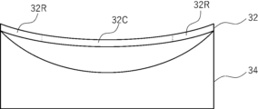
- a precursor film 32 with a convex shape transferred onto a mold 30 having a convex molding surface is obtained.
- the peripheral portion 32R of the precursor film 32 is more likely to be stretched than the central portion 32C.
- the surface of the planar precursor film on the light absorption anisotropic layer side is placed on the molding surface side of the mold.
- a substrate having a concave molded surface with a radius of curvature smaller than the radius of curvature of the convex molded surface is used, and the surface of the precursor film having the convex shape transferred thereto obtained by step 1A opposite to the surface that was in contact with the mold in step 1A is placed on the molded surface of the substrate, and the precursor film having the convex shape transferred thereto is deformed along the molded surface of the concave shape to produce a laminate.
- the radius of curvature of the molded surface of the substrate 34 having a concave molded surface used in step 2A is smaller than the radius of curvature of the molded surface of the mold 30 having a convex molded surface used in step 1A.
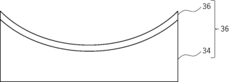
- step 2A first, as shown in FIG. 11, the precursor film 32 obtained in step 1A is placed on the substrate 34 having a molded surface with a smaller radius of curvature than the mold 30 used in step 1A.
- the precursor film 32 is placed on the substrate 34, the surface of the precursor film 32 opposite to the surface that was in contact with the mold 30 is placed on the molded surface of the substrate 34.
- the precursor film 32 is deformed so as to conform to the molding surface of the substrate 34, to obtain a laminate 36 having a curved surface shape.
- an adhesive layer is disposed between the substrate and the optically absorptive anisotropic layer.
- the central portion of the film is usually more easily stretched than the peripheral portion.
- the peripheral portion of the precursor film is more easily stretched than the central portion
- step 2A the central portion of the precursor film is more easily stretched than the peripheral portion. Therefore, when steps 1A and 2A are performed, the central portion and the peripheral portion are stretched to the same extent, and as a result, variation in intermolecular spacing is less likely to occur within the plane of the optically absorptive anisotropic layer in the obtained laminate 36, and as a result, a laminate that satisfies requirement X is obtained.
- a heating process may be performed on the precursor film, if necessary.
- the heating temperature during the heating process is appropriately selected to be optimal depending on the material and film thickness of the precursor film used.
- the heating temperature is preferably equal to or higher than the glass transition temperature of the optically absorptive anisotropic layer in the precursor film.
- the heating temperature is preferably within (the glass transition temperature of the optically absorptive anisotropic layer + 100°C).
- the method of deforming the precursor film along the molding surface is not particularly limited, but examples include a method of deforming the precursor film by vacuum drawing and a method of deforming the precursor film by applying pressure. Furthermore, when an adhesive layer is used as the adhesion layer, depending on the type of adhesive layer, a treatment for hardening the adhesive layer (for example, exposure treatment, etc.) may be carried out after step 2A or step 2B.
- the radius of curvature of the molding surface of the mold used in step 2A is smaller than the radius of curvature of the molding surface of the substrate used in step 1A.
- the ratio (CA2/CA1) of the radius of curvature (CA2) of the molding surface of the substrate used in step 2A to the radius of curvature (CA1) of the molding surface of the mold used in step 1A is selected from the optimum values according to the laminate to be manufactured, and is preferably 0.6 to 0.9, and more preferably 0.7 to 0.85.
- the smallest radius of curvature is regarded as the above-mentioned "radius of curvature of the molding surface of the mold used in step 1A.” Furthermore, in cases where the radius of curvature varies depending on the position on the molding surface of the substrate used in step 2A, the smallest radius of curvature is defined as the above-mentioned "radius of curvature of the molding surface of the substrate used in step 2A.”
- the radius of curvature of the molding surface of the substrate used in step 2B is smaller than the radius of curvature of the molding surface of the mold used in step 1B.
- the ratio (CB2/CB1) of the radius of curvature (CB2) of the molding surface of the substrate used in step 2B to the radius of curvature (CB1) of the molding surface of the mold used in step 1B is selected from the optimum values according to the optically absorptive anisotropic layer to be produced, and is preferably 0.6 to 0.9, and more preferably 0.7 to 0.85.
- the smallest radius of curvature is regarded as the "radius of curvature of the molding surface of the mold used in step 1B." Furthermore, in the case where the radius of curvature varies depending on the position on the molding surface of the substrate used in step 2B, the smallest radius of curvature is defined as the above-mentioned "radius of curvature of the molding surface of the substrate used in step 2B.”
- Method 2 is a method in which the planar precursor film is heated and molded with a distribution of heating temperature in the in-plane direction during molding.
- a first embodiment of Method 2 includes a production method including the steps of heating a planar precursor film so that the heating temperature of the peripheral portion surrounding the central portion of the planar precursor film is higher than the heating temperature of the central portion of the planar precursor film, and using a substrate having a concave molding surface, the surface of the heated planar precursor film opposite the light absorption anisotropic layer side (the surface of the adhesive layer or bonding layer) is made to be the molding surface side of the substrate having a concave molding surface, and the heated planar precursor film is deformed along the molding surface to produce a laminate.
- a second aspect of Method 2 includes a manufacturing method including the steps of heating a planar precursor film so that the heating temperature of the peripheral portion surrounding the central portion of the planar precursor film is lower than the heating temperature of the central portion of the planar precursor film, and using a substrate having a convex molding surface, the surface of the heated planar precursor film opposite the light absorption anisotropic layer side (the surface of the adhesive layer or bonding layer) is made to be the molding surface side of the substrate having a convex molding surface, and the heated planar precursor film is deformed along the molding surface to produce a laminate.
- the method for manufacturing the laminate can include an embodiment that includes a step of producing a laminate by imparting a temperature distribution in the in-plane direction of a planar precursor film including an optically absorptive anisotropic layer and an adhesive layer or bonding layer, and by making the surface of the precursor film opposite to the optically absorptive anisotropic layer side (the surface of the adhesive layer or bonding layer) the molding surface side of a substrate having a curved molding surface, and deforming the precursor film along the molding surface of the substrate.
- the first embodiment of Method 2 will be representatively described below with reference to the drawings.
- the central portion of the film is more easily stretched than the peripheral portion, and the intermolecular spacing is more likely to increase.
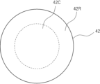
- the heating temperature of the peripheral portion 42R of the planar precursor film 42 arranged on a substrate 40 having a concave molding surface is made higher than the heating temperature of the central portion 42C, so that the peripheral portion 42R is made easier to stretch when the precursor film 42 is deformed along the molding surface.
- the central portion in molding using a substrate having a concave molding surface, the central portion is usually more easily stretched than the peripheral portion, but by changing the heating conditions for the central portion and the peripheral portion, the central portion is made less likely to stretch and the peripheral portion is made easier to stretch.
- the peripheral portion in the second aspect of Method 2, whereas in general, when a substrate having a convex molding surface is used for molding, the peripheral portion is more easily stretched than the central portion, by changing the heating conditions for the central portion and the peripheral portion, the peripheral portion is made less likely to stretch and the central portion is made more easily stretched.
- the optimum heating conditions for the precursor film are appropriately selected depending on the type of material of the precursor film used and the shape of the curved surface portion.
- the heating temperature is preferably equal to or higher than the glass transition temperature of the optically absorptive anisotropic layer in the precursor film.
- the upper limit of the heating temperature is not particularly limited, but is preferably within (the glass transition temperature of the optically absorptive anisotropic layer + 100°C).
- the heating method in method 2 is not particularly limited, but examples include heating by contact with a heated solid, heating by contact with a heated liquid, heating by contact with a heated gas, heating by infrared radiation, and heating by microwave radiation. Of these, heating by infrared radiation, which allows heating remotely just before molding, is preferred.
- the wavelength of the infrared rays used for heating is preferably 1.0 to 30.0 ⁇ m, and more preferably 1.5 to 5 ⁇ m.
- IR (infrared) light sources include near-infrared lamp heaters in which a tungsten filament is enclosed in a quartz tube, and wavelength control heaters in which quartz tubes are multiplexed and a part between the quartz tubes is cooled with air.
- Methods for providing an intensity distribution of infrared irradiation include a method of varying the density of the IR light source arrangement, and a method of placing a filter with a patterned transmittance for infrared light between the IR light source and the planar precursor film.
- filters with a patterned transmittance include those in which metal is deposited on glass, those in which the reflection band of a cholesteric liquid crystal layer is made infrared, those in which the reflection band is made infrared with a dielectric multilayer film, and ink that absorbs infrared rays.
- the temperature control of the planar precursor film is controlled by the intensity of infrared irradiation, and is controlled by the infrared irradiation time and the illuminance of infrared irradiation.
- the temperature of the planar precursor film is monitored using a non-contact radiation thermometer and a thermocouple, and it is possible to mold it at a target temperature.
- a treatment for hardening the adhesive layer for example, exposure treatment, etc. may be carried out after deformation.
- the laminate of the present invention may include layers other than the above-mentioned substrate, pressure-sensitive adhesive layer, adhesive layer, and optically absorptive anisotropic layer.
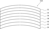
- the laminate 50A includes, in this order, a half mirror 52, a base material 54, an adhesive layer 56, a cholesteric liquid crystal layer 58, a positive C plate 60, a retardation layer 62 having a function of converting linearly polarized light into circularly polarized light, and a light absorption anisotropic layer 64.
- the laminate 50A corresponds to an embodiment having a cholesteric liquid crystal layer.
- the laminate 50B includes, in this order, a half mirror 52, a base material 54, an adhesive layer 56, a positive C plate 60, a retardation layer 62 having a function of converting linearly polarized light into circularly polarized light, a reflective linear polarizer 66, and an optically absorptive anisotropic layer 64.
- the laminate 50B corresponds to an embodiment having a retardation layer and a reflective linear polarizer. As shown in FIGS. 15 and 16, all of the members included in the stack 50A and the stack 50B have a curved surface.
- the angle between the slow axis of the retardation layer 62 and the transmission axis of the light absorptive anisotropic layer 64 is preferably within the range of 45° ⁇ 10°.
- the laminate 50A and the laminate 50B include two retardation layers, namely, a retardation layer 62 and a positive C plate 60.
- the retardation layer is not limited to a retardation layer having a function of converting linearly polarized light into circularly polarized light and a positive C plate, and may be in another form.
- a retardation layer having a function of converting linearly polarized light into circularly polarized light may be disposed on the side opposite to the retardation layer 62 of the optically absorptive anisotropic layer 64 of the laminate 50A. Also, a retardation layer having a function of converting linearly polarized light into circularly polarized light may be disposed on the side opposite to the reflective linear polarizer 66 of the optically absorptive anisotropic layer 64 of the laminate 50B. A surface antireflection layer may be further disposed on the side of the optically absorptive anisotropic layer 64 of the laminate 50A opposite to the retardation layer 62.
- a surface antireflection layer may be further disposed on the side of the optically absorptive anisotropic layer 64 of the laminate 50B opposite to the reflective linear polarizer 66.
- the laminate 50A and the laminate 50B may further include an alignment film disposed adjacent to the light absorptive anisotropic layer 64.
- the laminates 50A and 50B are suitably applied to a virtual reality display device, which will be described later.
- the structures of the base material 54, the adhesive layer 56 and the optically absorptive anisotropic layer 64 are as described above. Other members contained in the laminate will be described in detail below.
- the half mirror may be, for example, a conventionally known half mirror that transmits approximately half of the incident light and reflects the remaining half.
- the transmittance of the half mirror is preferably 50 ⁇ 30%, and more preferably 50 ⁇ 10%.
- the type of the half mirror is not particularly limited, but examples of the half mirror include a reflective layer made of a metal, such as silver or aluminum.
- the thickness of the half mirror is preferably from 1 to 20 nm, more preferably from 2 to 10 nm, and further preferably from 3 to 6 nm.
- the cholesteric liquid crystal layer is an optical member that separates incident light into right-handed circularly polarized light and left-handed circularly polarized light, specularly reflects one of the circularly polarized light, and transmits the other circularly polarized light.
- the cholesteric liquid crystal layer may be a cholesteric liquid crystal layer formed by fixing a cholesteric liquid crystal phase.
- the cholesteric liquid crystal layer is preferable as an optical film used for curved surface molding because it suppresses the decrease in polarization degree and the distortion of the polarization axis when it is stretched or molded into a three-dimensional shape. In addition, the decrease in polarization degree caused by the distortion of the polarization axis is unlikely to occur.
- the cholesteric liquid crystal layer preferably has at least a blue light reflecting layer having a reflectance of 40% or more at a wavelength of 460 nm, a green light reflecting layer having a reflectance of 40% or more at a wavelength of 550 nm, a yellow light reflecting layer having a reflectance of 40% or more at a wavelength of 600 nm, and a red light reflecting layer having a reflectance of 40% or more at a wavelength of 650 nm.
- This configuration is preferable because it can exhibit high reflection characteristics over a wide wavelength range in the visible range.
- the above reflectances are reflectances when non-polarized light is incident on the cholesteric liquid crystal layer at each wavelength.
- the cholesteric liquid crystal layer may have a pitch gradient structure in which the helical pitch of the cholesteric liquid crystal phase changes continuously in the thickness direction.
- the cholesteric liquid crystal layer a cholesteric liquid crystal layer formed by fixing a cholesteric liquid crystal phase containing rod-shaped liquid crystal compounds, in combination with a cholesteric liquid crystal layer formed by fixing a cholesteric liquid crystal phase containing discotic liquid crystal compounds.
- the cholesteric liquid crystal phase containing rod-shaped liquid crystal compounds has a positive Rth
- the cholesteric liquid crystal phase containing discotic liquid crystal compounds has a negative Rth, so that the Rths cancel each other out, and the occurrence of ghosts can be suppressed even for light incident from an oblique direction, which is preferable.
- the thickness of the cholesteric liquid crystal layer is not particularly limited, but from the viewpoint of thinning, it is preferably 30 ⁇ m or less, and more preferably 15 ⁇ m or less. There is no particular lower limit, and it is often 1 ⁇ m or more.
- the positive C plate is a type of retardation layer.
- the positive C plate is a retardation layer having substantially zero in-plane retardation and a negative retardation in the thickness direction, and functions as an optical compensation layer for increasing the degree of polarization of transmitted light with respect to obliquely incident light.
- the in-plane retardation of the positive C plate at a wavelength of 550 nm is preferably 10 nm or less.
- the retardation in the thickness direction of the positive C plate at a wavelength of 550 nm is preferably ⁇ 600 to ⁇ 40 nm.
- the material constituting the positive C plate is not particularly limited, but it is preferable that the plate be formed from a composition containing a liquid crystal compound.
- a positive C plate can be obtained by vertically aligning rod-shaped polymerizable liquid crystal compounds contained in a polymerizable liquid crystal composition and fixing the alignment state by polymerization. It can also be formed from a composition containing a side-chain polymer liquid crystal compound as the liquid crystal compound.
- the thickness of the positive C plate is not particularly limited, but from the viewpoint of thinness, it is preferably 0.5 to 10 ⁇ m, and more preferably 0.5 to 5 ⁇ m.
- a retardation layer having a function of converting linearly polarized light into circularly polarized light (hereinafter, also simply referred to as a "specific retardation layer”) is one type of retardation layer.
- the specific retardation layer is not particularly limited as long as it has a function of converting linearly polarized light into circularly polarized light, and an example of the specific retardation layer is a ⁇ /4 plate.
- a ⁇ /4 plate is a plate having a ⁇ /4 function, specifically, a plate having the function of converting linearly polarized light of a certain wavelength (preferably visible light) into circularly polarized light (or circularly polarized light into linearly polarized light).
- the in-plane retardation of the ⁇ /4 plate at a wavelength of 550 nm is not particularly limited, but is preferably from 120 to 150 nm, more preferably from 125 to 145 nm, and even more preferably from 135 to 140 nm.
- a retardation layer having an in-plane retardation at a wavelength of 550 nm that is 3/4 or 5/4 of any wavelength of visible light is also preferable.
- the specific retardation layer may have reverse wavelength dispersion, which means that the retardation value at a wavelength increases as the wavelength increases.
- the specific retardation layer may have a multi-layer structure, and a specific example of such a structure is a broadband ⁇ /4 plate formed by laminating a ⁇ /4 plate and a ⁇ /2 plate.
- the angle between the slow axis of the specific retardation layer and the absorption axis of the light absorptive anisotropic layer is not particularly limited, but is preferably within the range of 45° ⁇ 10°.
- the specific retardation layer may be a layer formed by fixing liquid crystal compounds that are twisted and aligned with the thickness direction as the helical axis.
- a retardation layer having a layer formed by fixing rod-shaped liquid crystal compounds or discotic liquid crystal compounds that are twisted and aligned with the thickness direction as the helical axis.
- the thickness of the specific retardation layer is not particularly limited, but is preferably 0.1 to 8 ⁇ m, and more preferably 0.3 to 5 ⁇ m.
- the laminate of the present invention may have a front-surface antireflection layer.
- the front-surface antireflection layer is preferably disposed on the outermost surface side.
- the front-surface antireflection layer may be disposed on only one surface side of the laminate, or on both surfaces.
- the type of the front-surface antireflection layer is not particularly limited, but from the viewpoint of further reducing the reflectance, a moth-eye film and an AR (anti-reflection) film are preferred.
- a moth-eye film is preferred because it can maintain high antireflection performance even if the film thickness varies due to stretching and molding.
- the laminate of the present invention may have an alignment layer.
- the alignment layer is preferably adjacent to the light absorbing anisotropic layer.
- the type of the alignment film is not particularly limited, and can be formed by, for example, rubbing treatment of an organic compound (preferably a polymer), oblique deposition of an inorganic compound, formation of a layer having microgrooves, or accumulation of an organic compound (e.g., ⁇ -tricosanoic acid, dioctadecylmethylammonium chloride, methyl stearate) by the Langmuir-Blodgett method (LB film).
- LB film Langmuir-Blodgett method
- a rubbed alignment film can be mentioned.
- an alignment film is also known which exhibits an alignment function when an electric field is applied, a magnetic field is applied, or light (preferably polarized light) is irradiated.
- a photo-alignment film is also preferable.
- the alignment film is preferably a layer formed from a composition containing a compound having an active hydrogen reactive group (composition for forming an alignment film).
- the active hydrogen reactive group include the groups described above.
- the compound preferably further has an active hydrogen-containing group in addition to the active hydrogen-reactive group.
- active hydrogen-containing group refers to a functional group that contains active hydrogen. Examples of the active hydrogen-containing group include a hydroxyl group, a carboxyl group, an amino group, a mercapto group, a primary amide group, a secondary amide group, and a hydrazide group.
- silane coupling agent examples include the compounds described in paragraphs 0050 and 0051 of JP-A-2022-120660.
- the composition for forming an alignment film preferably contains a polymer including a structural unit having a photoreactive group and a structural unit having a polymerizable group.
- the structural unit having a photoreactive group is derived from a monomer having at least one photoreactive group.
- the photoreactive group refers to a group that generates liquid crystal alignment ability by light irradiation. Specifically, it means a group that generates a photoreaction that is the origin of liquid crystal alignment ability by light irradiation, such as a dimerization reaction, an isomerization reaction, or a photodecomposition reaction, and induces alignment of polymer molecules.
- the structural unit having a polymerizable group is derived from a monomer having at least one polymerizable group.
- the polymerizable group means a group involved in a polymerization reaction, and includes a thermally polymerizable group and a photopolymerizable group, but the polymerizable group contained in the structural unit having a polymerizable group is preferably a photopolymerizable group.
- Examples of the polymer include those described in paragraphs 0020 to 0041 of JP-A-2021-196514.
- FIG. 17 is a schematic diagram showing an example of the configuration of a virtual reality display device.
- a virtual reality display device 80 shown in Fig. 17 includes, from the right side in the figure, an image display panel 82, a circular polarizing plate 84, and a laminate 50A of the present invention.
- the laminate 50A used in Fig. 17 includes, in this order, a half mirror 52, a base material 54, an adhesive layer 56, a cholesteric liquid crystal layer 58, a positive C plate 60, a retardation layer 62 having a function of converting linearly polarized light into circularly polarized light, and a light absorption anisotropic layer 64.
- a light ray 92 emitted from an image display panel 82 passes through a circular polarizing plate 84 to become circularly polarized light, and passes through a half mirror 52.
- the light ray passes through a substrate 54, enters a cholesteric liquid crystal layer 58, is reflected, passes through the substrate 54 again, is reflected again by the half mirror 52, passes through the substrate 54 again, and enters the cholesteric liquid crystal layer 58.
- the circular polarization state of the light ray does not change when reflected by the cholesteric liquid crystal layer 58, and when reflected by the half mirror 52, it changes to a circularly polarized light having a rotation direction opposite to that of the circularly polarized light when it entered the cholesteric liquid crystal layer 58. Therefore, the light ray passes through the cholesteric liquid crystal layer 58 and is visually recognized by the user. Furthermore, when the light ray is reflected by the half mirror 52, the image is enlarged because the half mirror 52 is shaped as a concave mirror, and the user can visually recognize the enlarged virtual image.
- the above-mentioned mechanism is called a round-trip optical system, a folded optical system, or the like.
- the light absorbing anisotropic layer 64 included in the laminate 50A functions as a so-called linear polarizer, blocking light that is unnecessarily transmitted through the cholesteric liquid crystal layer 58 and preventing it from becoming leakage light (ghost) and being observed by the user of the virtual reality display device.
- the laminate 50B may be used in place of the laminate 50A.
- the image display panel 82 is, for example, a known image display panel (display panel) such as an organic electroluminescence display panel.
- the image display panel 82 emits an unpolarized image (image light).
- the unpolarized image emitted by the image display panel 82 passes through the circular polarizer 84 and is converted into circularly polarized light.
- Example 1 ⁇ Preparation of Absorptive Polarizer Film 1> (Preparation of Support)
- the following composition was put into a mixing tank, stirred, and further heated at 90°C for 10 minutes.
- the obtained composition was then filtered through a filter paper with an average pore size of 34 ⁇ m and a sintered metal filter with an average pore size of 10 ⁇ m to prepare a dope.
- the solid content concentration of the dope was 23.5 mass%
- the amount of the plasticizer added was the ratio relative to the cellulose acylate
- the dope prepared above was cast using a drum film-forming machine.
- the dope was cast from a die so that it was in contact with a metal support cooled to 0°C, and then the resulting web (film) was peeled off from the drum.
- the drum was made of SUS (stainless steel).
- the web (film) obtained by casting was peeled off from the drum, and then dried for 20 minutes in a tenter apparatus, which clips both ends of the web with clips and transports the web at 30 to 40° C.
- the web was then post-dried by zone heating while being transported with rolls.
- the web obtained was knurled and then wound up to obtain cellulose acylate film A1.
- the obtained cellulose acylate film A1 had a thickness of 60 ⁇ m, an in-plane retardation Re(550) at a wavelength of 550 nm of 1 nm, and a retardation in the thickness direction Rth(550) at a wavelength of 550 nm of 35 nm.
- the photo-alignment film-forming composition B1 described later was continuously applied onto the cellulose acylate film A1 using a wire bar.
- the cellulose acylate film A1 on which the coating film was formed was dried with hot air at 140° C. for 120 seconds, and then the coating film was irradiated with polarized ultraviolet light (10 mJ/cm 2 , using an ultra-high pressure mercury lamp) to form a photo-alignment film B1, thereby obtaining a TAC (triacetyl cellulose) film with a photo-alignment film.
- the thickness of the photo-alignment film B1 was 1.5 ⁇ m.
- Photoalignment compound PA-1 (weight average molecular weight: 32000) (In the formula, the numerical value for each repeating unit represents the content (mass%) of each repeating unit relative to all repeating units.)
- Polymerizable polymer PA-2 (weight average molecular weight: 18000) (In the formula, the numerical values of a, b, and c represent the content (mass%) of each repeating unit relative to the total repeating units.)
- a composition C1 for forming an optically absorptive anisotropic layer having the following composition was continuously applied with a wire bar to form a coating film.
- the coating was then heated at 110° C. for 120 seconds, and the coating was then rapidly cooled to room temperature (23° C.).
- ultraviolet light was irradiated at an exposure dose of 1000 mJ/cm 2 (365 nm standard) using a high pressure mercury lamp to form an optically absorptive anisotropic layer C1 having a thickness of 1.7 ⁇ m.
- the content of the dichroic material in the light absorption anisotropic layer C1 was 80 mg/cm 3 .
- composition C1 for forming an optically absorptive anisotropic layer was prepared by dissolving the components described below at 80° C. for 2 hours with stirring, and filtering the mixture through a 0.45 ⁇ m filter.
- ⁇ Optically absorptive anisotropic layer forming composition C1 ⁇ 75 parts by mass of liquid crystal compound L1 shown below 25 parts by mass of liquid crystal compound L2 shown below 3 parts by mass of dichroic substance A1 shown below 3 parts by mass of dichroic substance A2 shown below 1 part by mass of dichroic substance A3 shown below 1 part by mass of dichroic substance A4 shown below 2-dimethylamino-2-benzyl-1-(4-morpholinophenyl) Butan-1-one (Irgacure 369, manufactured by BASF) 6 parts by mass Polyacrylate compound (BYK-361N, (manufactured by BYK Chemie) 1.2 parts by mass Laromer (registered trademark) LR-9000 2 parts by mass o-x
- Dichroic substance A1 (maximum absorption wavelength 385 nm)
- Dichroic substance A2 (maximum absorption wavelength 507 nm)
- Dichroic substance A3 (maximum absorption wavelength 590 nm)
- Dichroic substance A4 (maximum absorption wavelength 590 nm)
- a protective layer-forming coating solution D1 having the following composition was continuously coated with a wire bar. Thereafter, the film was dried with hot air at 80°C for 5 minutes and irradiated with 300 mJ using an LED (light emitting diode) lamp (center wavelength 365 nm) under irradiation conditions of 300 mJ to obtain a laminate having a protective layer D1 made of polyvinyl alcohol (PVA) having a thickness of 0.6 ⁇ m, i.e., an absorptive polarizer film 1 having a cellulose acylate film A1 (support), a photo-alignment film B1, a light absorption anisotropic layer C1, and a protective layer D1 adjacent to each other in this order.
- PVA polyvinyl alcohol
- Modified polyvinyl alcohol (weight average molecular weight: 28,000) (In the following formula, the numerical value for each repeating unit represents the content (mass %) of each repeating unit relative to all repeating units.)
- the coating solution E1 for forming a photo-alignment film having the following composition was continuously applied onto the above-mentioned cellulose acylate film A1 using a wire bar.
- the cellulose acylate film A1 on which the coating film was formed was dried with hot air at 140° C. for 120 seconds, and then the coating film was irradiated with polarized ultraviolet light (10 mJ/cm 2 , using an ultra-high pressure mercury lamp) to form a photo-alignment film E1 with a thickness of 0.2 ⁇ m, thereby obtaining a TAC film with a photo-alignment film.
- Coating liquid E1 for forming photo-alignment film ⁇ ⁇ 100.00 parts by mass of polymer PA-2 shown below ⁇ 5.00 parts by mass of thermal cationic polymerization initiator PAG-1 shown above ⁇ 0.005 parts by mass of acid generator CPI-110TF shown below ⁇ 16.50 parts by mass of isopropyl alcohol ⁇ 1072.00 parts by mass of butyl acetate ⁇ 268.00 parts by mass of methyl ethyl ketone
- Polymer PA-2 (weight average molecular weight: 45000) (In the following formula, the numerical value for each repeating unit represents the content (mass %) of each repeating unit relative to all repeating units.)
- the composition F1 having the following composition was applied onto the photo-alignment film E1 using a bar coater.
- the coating film formed on the photo-alignment film E1 was heated to 120°C with hot air, and then cooled to 60°C.
- the coating film was then irradiated with 100mJ/ cm2 ultraviolet light at a wavelength of 365nm using a high-pressure mercury lamp under a nitrogen atmosphere, and then irradiated with 500mJ/ cm2 ultraviolet light while heating to 120°C, thereby fixing the alignment of the liquid crystal compound, and a retardation layer film 1 having a positive A plate F1 was produced.
- the positive A plate F1 had a thickness of 2.5 ⁇ m and an Re(550) of 144 nm.
- the positive A plate satisfied the relationship Re(450) ⁇ Re(550) ⁇ Re(650).
- Re(450)/Re(550) was 0.82.
- the positive A plate corresponds to a so-called ⁇ /4 plate.
- Polymerizable liquid crystal compound LA-1 (tBu stands for tertiary butyl group)
- Polymerizable liquid crystal compound LA-4 (Me stands for methyl group)
- Leveling agent T-1 weight average molecular weight: 25,000 (In the following formula, the numerical value for each repeating unit represents the content (mass %) of each repeating unit relative to all repeating units.)
- ⁇ Preparation of Retardation Layer Film 2 Having Positive C Plate> As the temporary support, the above-mentioned cellulose acylate film A1 was used. The cellulose acylate film A1 was passed through a dielectric heating roll at a temperature of 60°C to raise the surface temperature of the film to 40°C, and then an alkaline solution having the composition shown below was applied to one side of the film in an amount of 14 ml/ m2 using a bar coater, heated to 110°C, and transported under a steam-type far-infrared heater manufactured by Noritake Co., Limited for 10 seconds. Next, 3 ml/ m2 of pure water was applied onto the film using the same bar coater. Next, after repeating washing with water using a fountain coater and draining with an air knife three times, the film was transported to a drying zone at 70° C. for 10 seconds and dried to prepare an alkaline saponified cellulose acylate film A1.
- the coating solution G1 for forming an alignment film having the following composition was continuously applied onto the above-mentioned alkaline saponification-treated cellulose acylate film A1 using a #8 wire bar.
- the resulting film was dried with hot air at 60°C for 60 seconds and then with hot air at 100°C for 120 seconds to form an alignment film G1.
- Alignment film forming coating solution G1 ⁇ - Polyvinyl alcohol (Kuraray, PVA103) 2.4 parts by weight - Isopropyl alcohol 1.6 parts by weight - Methanol 36 parts by weight - Water 60 parts by weight
- a coating solution H1 for forming a positive C plate having the following composition was applied onto an alignment film G1, and the resulting coating film was aged at 60° C. for 60 seconds.
- the coating film was then irradiated with ultraviolet light at 1000 mJ/cm 2 using an air-cooled metal halide lamp (manufactured by Eye Graphics Co., Ltd.) at 70 mW/cm 2 under air to fix the alignment state, thereby vertically aligning the liquid crystal compound, and a retardation layer film 2 having a positive C plate H1 with a thickness of 0.5 ⁇ m was produced.
- the Rth(550) of the obtained positive C plate was ⁇ 60 nm.
- Compound B03 (weight average molecular weight: 15000) (In the following formula, the numerical value for each repeating unit represents the content (mass %) of each repeating unit relative to all repeating units.)
- a composition for forming a second optically anisotropic layer 1 was prepared by dissolving the following rod-shaped liquid crystal compound A (83 parts by mass), the following rod-shaped liquid crystal compound B (15 parts by mass), the following rod-shaped liquid crystal compound C (2 parts by mass), an acrylate monomer (A-400, manufactured by Shin-Nakamura Chemical Co., Ltd.) (4.2 parts by mass), the following polymer A (2 parts by mass), the following vertical alignment agent A (1.9 parts by mass), the following photopolymerization initiator A (5.1 parts by mass), the following photoacid generator A (3 parts by mass), and the following photoalignable polymer B (0.8 parts by mass) in methyl isobutyl ketone (567 parts by mass).
- the prepared second optical anisotropic layer forming composition 1 was applied to the above-mentioned cellulose acylate film A1 with a wire bar of #3.0, heated at 70° C. for 2 minutes, and irradiated with ultraviolet light of 150 mJ/cm 2 at an oxygen concentration of less than 100 ppm. Then, annealed at 120° C. for 1 minute to form a second optical anisotropic layer.
- the second optically anisotropic layer was a positive C plate satisfying the formula (C1) nz>nx ⁇ ny, and had a thickness of about 0.5 ⁇ m.
- Polymer A (weight average molecular weight: 57,000) (In the following formula, the numerical value for each repeating unit represents the content (mass %) of each repeating unit relative to all repeating units.)
- the obtained second optically anisotropic layer was irradiated with 7.9 mJ/cm 2 (wavelength: 313 nm) of UV light (ultra-high pressure mercury lamp; UL750; manufactured by HOYA) through a wire grid polarizer at room temperature to impart an alignment function.
- the rod-shaped liquid crystal compound A (7.0 parts by mass), the rod-shaped liquid crystal compound B (1.3 parts by mass), the rod-shaped liquid crystal compound C (0.2 parts by mass), the rod-shaped liquid crystal compound D (21.2 parts by mass), the rod-shaped liquid crystal compound E (26.1 parts by mass), the rod-shaped liquid crystal compound F (29.0 parts by mass), the compound G (15.3 parts by mass), the polymerizable compound M1 (5 parts by mass), the photopolymerization initiator A (0.5 parts by mass), and the polymer C (0.1 parts by mass) were dissolved in cyclopentanone (175 parts by mass), methyl ethyl ketone (50 parts by mass), and ethyl laurate (10 parts by mass) as solvents to prepare a first optically anisotropic layer-forming composition 1.
- composition 1 for forming the first optically anisotropic layer was applied on the second optically anisotropic layer formed previously with a wire bar coater #7 to form a composition layer.
- the formed composition layer was once heated to 120°C on a hot plate, and then cooled to 60°C to stabilize the orientation.
- the film temperature was kept at 60°C under a nitrogen atmosphere (oxygen concentration less than 100 ppm) using an ultra-high pressure mercury lamp, and the orientation was fixed by the first ultraviolet irradiation (80 mJ/cm 2 ) with the film temperature kept at 100°C and the second ultraviolet irradiation (300 mJ/cm 2 ), forming a first optically anisotropic layer having a thickness of 2.8 ⁇ m, and a retardation layer film 3 was produced.
- the first optically anisotropic layer is a positive A plate that satisfies the formula (A1) nx>ny ⁇ nz, and corresponds to a so-called ⁇ /4 plate.
- Polymer C (weight average molecular weight: 25,000) (In the following formula, the numerical value for each repeating unit represents the content (mass %) of each repeating unit relative to all repeating units.)
- Reflective layer coating solution R-1 The composition shown below was stirred in a container kept at 70° C. to prepare a coating solution R-1 for a reflective layer, where R represents a coating solution using a rod-like liquid crystal compound.
- the numerical values are mass %.
- R is a group bonded via an oxygen atom.
- the average molar absorption coefficient of the above rod-shaped liquid crystal at wavelengths of 300 to 400 nm was 140/mol cm.
- Surfactant F1 weight average molecular weight: 25,000 (The content ratio (mass ratio) of the repeating unit shown on the upper side to the repeating unit shown on the lower side in the following formula was 76:24.)
- Chiral agent A is a chiral agent whose helical twisting power (HTP) is reduced by light.
- Reflective layer coating solution R-2 The coating solution was prepared in the same manner as in the coating solution R-1 for the reflective layer, except that the amount of chiral agent A added was changed as shown in Table 1 below.
- Table 1 Amount of chiral agent in coating solution containing rod-shaped liquid crystal compound.
- Light interference layer coating solution PA-1 The composition shown below was stirred in a container kept at 60° C. to prepare a coating solution for optical interference layer PA-1.
- Coating solution for optical interference layer PA-1 ⁇ Methyl isobutyl ketone 3011.0 parts by mass; Mixture X of the above rod-shaped liquid crystal compounds 100.0 parts by mass; Photopolymerization initiator C described below 5.1 parts by mass; Photoacid generator described below 3.0 parts by mass; Hydrophilic polymer described below 2.0 parts by mass; Vertical alignment agent described below 1.9 parts by mass; Viscosity reducer described below 4.2 parts by mass; Photoalignable polymer B described above 8.0 parts by mass; Stabilizer described below 0.2 parts by mass
- Hydrophilic polymer weight average molecular weight: 57,000 (In the following formula, the numerical value for each repeating unit represents the content (mass %) of each repeating unit relative to all repeating units.)
- a 60 ⁇ m-thick TAC (triacetyl cellulose) film (TG60, manufactured by Fuji Film Corporation) was prepared.
- the coating solution PA-1 for the optical interference layer prepared above was applied to the tack film using a wire bar coater, and then dried at 80°C for 60 seconds. Thereafter, in a low-oxygen atmosphere (100 ppm), the liquid crystal compound was cured by irradiating it with light from an ultraviolet LED lamp (wavelength 365 nm) at 78°C with an irradiation dose of 300 mJ/ cm2 , and at the same time, the cleavage group of the photo-alignable polymer B was cleaved.
- an ultraviolet LED lamp wavelength 365 nm
- the substrate was heated at 115°C for 25 seconds to remove the substituent containing a fluorine atom.
- the refractive index nI measured using an interference film thickness meter OPTM (manufactured by Otsuka Electronics, analyzed by the least squares method) was 1.57.
- the Rth measured at a wavelength of 550 nm using an Axoscan (manufactured by Axometrics) was -9 nm.
- polarized UV (wavelength 313 nm) with an illuminance of 7 mW/cm 2 and an exposure dose of 7.9 mJ/cm 2 was irradiated from the positive C plate side.
- the polarized UV with a wavelength of 313 nm was obtained by passing ultraviolet light emitted from a mercury lamp through a bandpass filter having a transmission band at a wavelength of 313 nm and a wire grid polarizer.
- the reflective layer coating solution R-1 prepared above was applied with a wire bar coater and then dried at 110° C. for 72 seconds.
- the blue light reflective layer made of a cholesteric liquid crystal layer was formed by curing the coating by irradiating light from a metal halide lamp with an illuminance of 80 mW/cm 2 and an exposure dose of 500 mJ/cm 2 at 100° C. under a low oxygen atmosphere (100 ppm or less). The light was irradiated from the cholesteric liquid crystal layer side in all cases. At this time, the coating thickness was adjusted so that the film thickness of the first blue light reflective layer after curing was 2.6 ⁇ m.
- the first blue light reflecting layer surface was subjected to a corona treatment at a discharge amount of 150 W ⁇ min/m 2 , and then the reflective layer coating solution D-1 was applied to the corona-treated surface with a wire bar coater.
- the coating film was then dried at 70° C. for 2 minutes, and the solvent was evaporated, followed by heating and aging at 115° C. for 3 minutes to obtain a uniform alignment state.
- the coating film was held at 45° C. and cured by irradiating it with ultraviolet light (300 mJ/cm 2 ) using a metal halide lamp under a nitrogen atmosphere, thereby forming a second blue light reflecting layer on the first blue light reflecting layer.
- the light irradiation was performed from the cholesteric liquid crystal layer side in all cases.
- the coating thickness was adjusted so that the film thickness of the second blue light reflecting layer after curing was 2.0 ⁇ m.
- the reflective layer coating solution D-2 was applied onto the second blue light reflective layer using a wire bar coater.
- the coating film was then dried at 70°C for 2 minutes, and after the solvent was evaporated, the coating film was heated and aged at 115°C for 3 minutes to obtain a uniform alignment state. Thereafter, the coating film was held at 45°C and cured by irradiating it with ultraviolet light (300 mJ/ cm2 ) using a metal halide lamp under a nitrogen atmosphere, thereby forming a green light reflective layer on the second blue light reflective layer. The light irradiation was performed from the cholesteric liquid crystal layer side in all cases. At this time, the coating thickness was adjusted so that the film thickness of the cured green light reflective layer was 2.7 ⁇ m.
- the coating solution R-2 for the reflective layer was applied onto the green light reflective layer using a wire bar coater, and then dried at 110°C for 72 seconds. Thereafter, the coating solution was cured by irradiating light from a metal halide lamp at 100°C with an illuminance of 80 mW and an irradiation dose of 500 mJ/ cm2 in a low-oxygen atmosphere (100 ppm or less), thereby forming a red light reflective layer on the green light reflective layer. The light irradiation was performed from the cholesteric liquid crystal layer side in all cases. At this time, the coating thickness was adjusted so that the film thickness of the red light reflective layer after curing was 3.4 ⁇ m.
- Table 3 shows the central reflection wavelength and film thickness for each reflective layer of the reflective circular polarizer that was fabricated.
- the central reflection wavelength is used to define the characteristics of a light reflective film with a reflection band that uses cholesteric liquid crystal, and refers to the midpoint of the spectral band that the film reflects. Specifically, it was obtained by calculating the average value of the short wavelength side and the long wavelength side wavelength that show half the peak reflectance.
- the central reflection wavelength central wavelength of reflected light
- optical laminate A0 was produced by the following procedure.
- the yellow light reflection layer side of the obtained reflective circular polarizer film 1 was attached to a PMMA film (50 ⁇ m) with an adhesive, and the temporary support (TG60) was peeled off.
- the positive C plate side of the obtained retardation layer film 2 was attached to the surface of the PMMA film attached to the reflective circular polarizer film 1 with an adhesive, and the support and the alignment film were peeled off.
- the positive A plate side of the obtained retardation layer film 1 was attached to the liquid crystal surface exposed by peeling off the alignment film with an adhesive, and the alignment film and the support were peeled off.
- an optical laminate A0 including a reflective circular polarizer/adhesive layer/PMMA film/adhesive layer/positive C plate/adhesive layer/positive A plate was produced.
- optical laminate B0 was produced by the following procedure.
- a broadband dielectric multilayer film (3M's trademark APF) was used as a reflective linear polarizer.
- the liquid crystal layer side of the retardation layer film 3 was attached to one surface of the APF with an adhesive, and the support was peeled off. In this way, an optical laminate B0 including a reflective linear polarizer/adhesive layer/positive A plate/positive C plate was produced.
- an adhesive layer was applied to the reflective circular polarizer side using an adhesive sheet, thereby obtaining an optical laminate C1 including, in this order, an adhesive layer/reflective circular polarizer/adhesive layer/PMMA film/adhesive layer/positive C plate/adhesive layer/positive A plate/adhesive layer/protective layer D1/light absorption anisotropic layer C1.
- this optical laminate C1 was set in a molding device. At this time, the optically absorbing anisotropic layer C1 was arranged so that it was on the lower side.
- the molding space in the molding device was composed of a box 1 and a box 2 partitioned by the optical laminate C1, and a mold 1 (a convex lens with a diameter of 50 mm and a radius of curvature of 60 mm) was arranged in the box 1 below the optical laminate C1 so that the convex surface was on the upper side.
- a transparent window was installed on the upper part of the box 2 above the optical laminate C1, and an IR light source for heating the optical laminate C1 was installed on the outside of the window.
- the inside of the box 1 and the inside of the box 2 were evacuated to 0.1 atmosphere or less by a vacuum pump.
- the optical laminate C1 molded into a convex shape was set in a molding device with the light absorption anisotropic layer C1 side facing up, upside down from the first molding. At this time, the area molded into a convex shape in the optical laminate C1 by the first molding was protruding downward. Just below the area molded into a convex shape in the light absorption anisotropic layer C1, a meniscus lens (diameter 50 mm, radius of curvature on the concave side 50 mm) with aluminum deposition on the convex side as the mold 2 was placed so that the concave side was facing up. Next, the inside of the box 1 and the inside of the box 2 were evacuated to 0.1 atmosphere or less by a vacuum pump.
- Example 1 a laminate molded into a curved surface (hereinafter also referred to as a "compound lens”) was obtained as Example 1.
- Example 2 A composite lens was obtained in the same manner as in Example 1, except that the liquid crystal compounds L1 and L2 in the composition C1 for forming an optically absorptive anisotropic layer were changed to the liquid crystal compounds L3 and L4, respectively.
- the composition obtained by changing the liquid crystal compounds L1 and L2 in the composition C1 for forming an optically absorptive anisotropic layer to liquid crystal compounds L3 and L4, respectively, is designated as composition C2 for forming an optically absorptive anisotropic layer.
- Example 3 A composite lens was obtained in the same manner as in Example 1, except that the composition for forming an optically absorptive anisotropic layer C1 was changed to the composition for forming an optically absorptive anisotropic layer C3.
- Example 4 A complex lens was obtained in the same manner as in Example 1, except that ⁇ Preparation of a Complex Lens (1)> was changed to the following ⁇ Preparation of a Complex Lens (2)>.
- optical laminate C1 was produced according to the same procedure as in ⁇ Production of a compound lens (1)> above. Next, this optical laminate C1 was set in a molding device. At this time, the optically absorbing anisotropic layer C1 was arranged so that the side was on the upper side.
- the molding space in the molding device was composed of a box 1 and a box 2 partitioned by the optical laminate C1, and a meniscus lens (diameter 40 mm, radius of curvature on the concave side 38 mm) with aluminum deposition on the convex side was arranged as a mold in the box 1 below the optical laminate C1 so that the concave side was on the upper side.
- a transparent window was installed on the upper side of the box 2 above the optically absorbing anisotropic layer C1, and an IR light source for heating the optical laminate C1 was installed on the outside of this.
- a circular pattern infrared reflection filter obtained by cutting out a cholesteric liquid crystal layer that reflects infrared rays with wavelengths of 2.2 ⁇ m to 3.0 ⁇ m with a reflectance of about 50% into a circular shape with a diameter of 1 inch was arranged.
- the center of the pattern infrared reflection filter was arranged so that it was at the center of the mold when viewed from directly above.
- Example 5 A composite lens was obtained in the same manner as in Example 4, except that the composition C1 for forming an optically absorptive anisotropic layer was changed to the composition C3 for forming an optically absorptive anisotropic layer.
- Example 6 A complex lens was obtained following the same procedure as in Example 4, except that the meniscus lens (diameter 40 mm, concave side curvature radius 38 mm) was changed to a meniscus lens (diameter 50 mm, concave side curvature radius 70 mm).
- Example 7 A composite lens was obtained in the same manner as in Example 6, except that the optical laminate D1 obtained in the latter step was used instead of the optical laminate C1.
- optical laminate D1 (Preparation of optical laminate D1)
- the APF side of the optical laminate B0 obtained above and the protective layer side of the absorptive polarizer film 1 were bonded together with an adhesive, and only the support of the absorptive polarizer film 1 was peeled off. However, the layers were laminated so that the transmission axis of the APF and the transmission axis of the light absorbing anisotropic layer were aligned.
- an adhesive layer was applied to the positive C plate side using an adhesive sheet. This resulted in an optical laminate D1 including an adhesive layer/positive C plate/positive A plate/adhesive layer/reflective linear polarizer/adhesive layer/protective layer D1/light absorbing anisotropic layer C1.
- Example 8 A complex lens was obtained following the same procedure as in Example 7, except that the meniscus lens (diameter 50 mm, concave side curvature radius 70 mm) was changed to a meniscus lens (diameter 50 mm, concave side curvature radius 78 mm).
- Example 9 A composite lens was obtained in the same manner as in Example 8, except that the optical laminate C2 obtained in the latter step was used instead of the optical laminate D1.
- an optical laminate C2 including an adhesive layer/reflective circular polarizer/adhesive layer/PMMA film/adhesive layer/positive C plate/adhesive layer/positive A plate/adhesive layer/protective layer D1/optical absorption anisotropic layer C1/adhesive layer/positive A plate/positive C plate/adhesive layer/PMMA film/UV adhesive layer/moth-eye layer was obtained.
- Example 10 A composite lens was obtained in the same manner as in Example 8, except that the optical laminate D2 obtained in the latter step was used instead of the optical laminate D1.
- an optical laminate D2 including an adhesive layer/positive C plate/positive A plate/adhesive layer/reflective linear polarizer/adhesive layer/protective layer D1/optical absorption anisotropic layer C1/adhesive layer/positive A plate/positive C plate/adhesive layer/PMMA film/UV adhesive layer/moth-eye layer was obtained.
- the optical laminate C1 was set in a molding device. At this time, the optically absorbing anisotropic layer C1 was arranged so that it was on the upper side.
- the molding space in the molding device was composed of a box 1 and a box 2 partitioned by the optical laminate C1, and a meniscus lens (diameter 50 mm, radius of curvature on the concave side 50 mm) with aluminum deposition on the concave side was arranged as a mold 2 in the box 1 below the optical laminate C1 so that the concave side was on the upper side.
- a transparent window was installed on the upper part of the box 2 above the optical laminate C1, and an IR light source for heating the optical laminate C1 was installed on the outside of this.
- a substrate (lens) in which the surface of the concave side of the meniscus lens was subjected to corona treatment was used as a curved substrate.
- the corona-treated surface was coated with a composition B1 for forming a photo-alignment film using a spin coater, and then dried with hot air at 140° C. for 120 seconds.
- the coating film was then irradiated with polarized ultraviolet light (10 mJ/cm 2 , using an ultra-high pressure mercury lamp) to form a photo-alignment film B1.
- the composition C1 for forming a light-absorbing anisotropic layer was continuously coated on the obtained photo-alignment film B1 using a spin coater to form a coating film.
- the coating film was heated at 110° C. for 120 seconds, and the coating film was rapidly cooled to room temperature (23° C.). Thereafter, a high pressure mercury lamp was used to irradiate ultraviolet light with an exposure dose of 1000 mJ/cm 2 (based on 365 nm) to form a light-absorbing anisotropic layer C1.
- the coating liquid D1 for forming a protective layer was continuously coated on the light-absorbing anisotropic layer C1 using a spin coater. Thereafter, the substrate was dried with hot air at 80° C.
- the laminate includes:
- the obtained curved polarization degree measurement sample X contains a photo-alignment film, a light absorption anisotropic layer, a protective layer, and a PMMA film, but it was confirmed that the photo-alignment film, the protective layer, and the PMMA film do not affect the polarization degree.
- the "degree of polarization corrected for luminosity” refers to a light source, a linear polarizer, and a curved absorptive polarizer film for measurement, which are placed in this order, and the transmittance in the wavelength range of 380 to 780 nm incident from the Fujitac TD80UL side is measured, and the transmittance values for every 5 nm between 380 and 780 nm are weighted and averaged using the Y value of the XYZ color matching function (color matching function of the CIE 1931 standard observer) standardized by the CIE (International Commission on Illumination).
- a calculated value A which is the product of the transmittance value measured every 5 nm between 380 and 780 nm and the Y value corresponding to the transmittance measurement wavelength, is calculated for each measurement wavelength, and the calculated values A obtained at each measurement wavelength are summed to calculate a total value B, and the obtained total value B is divided by the total value C of the Y values used above (total value B/total value C), thereby measuring the transmittance.
- linearly polarized light parallel to the transmission axis of the optically absorptive anisotropic layer is irradiated from the normal direction of the surface of the measurement sample, and the transmittance T1 is measured.
- the in-plane variation in the film thickness of the optically absorptive anisotropic layer in each of the composite lenses produced according to the procedures described in the above Examples 1 to 10 and Comparative Examples 1 and 2 was measured and evaluated according to the following criteria.
- the in-plane variation of film thickness was measured by the method described above. More specifically, the film thicknesses of 16 points of the light absorption anisotropic layer were calculated according to the procedure described above, and the in-plane variation was calculated using the values (see FIG. 4).
- the manufactured virtual reality display device (Fr product) was set in a high-temperature and high-humidity chamber and stored under conditions of 45° C. and 40% for 1000 hours.
- composition formulation indicates the type of liquid crystal composition used
- Composition 1 means composition C1 for forming an optically absorptive anisotropic layer
- Composition 2 means composition C2 for forming an optically absorptive anisotropic layer
- Composition 3 means composition C3 for forming an optically absorptive anisotropic layer.
- curvature radius indicates the radius of curvature of a laminate having a curved shape.
- P1 column indicates the value of the polarization degree P1.
- the " ⁇ P” column represents polarization degree P1 - polarization degree P2
- A means that polarization degree P1 - polarization degree P2 is 0.15% or less
- B means that polarization degree P1 - polarization degree P2 is more than 0.15% and 0.27% or less
- C means that polarization degree P1 - polarization degree P2 is more than 0.27%.
- the column “In-plane film thickness variation” shows the results of the thickness measurements.
- Laminate 12 Substrate 14 Adhesive layer 16 Light-absorption anisotropic layer 20 Mold having a concave molded surface 22 Film 24 Film to which a concave shape has been transferred 26, 30 Mold having a convex molded surface 28 Film to which a convex shape has been transferred 32 Precursor film to which a convex shape has been transferred 34, 40 Substrate having a concave molded surface 36 Laminate 42 Planar precursor film 50A, 50B Laminate 52 Half mirror 54 Substrate 56 Adhesive layer 58 Cholesteric liquid crystal layer 60 Positive C plate 62 Retardation layer having a function of converting linearly polarized light into circularly polarized light 64 Light-absorption anisotropic layer 66 Reflective linear polarizer 80 Virtual reality display device 82 Image display panel 84 Circular polarizer
Landscapes
- Physics & Mathematics (AREA)
- General Physics & Mathematics (AREA)
- Optics & Photonics (AREA)
- Engineering & Computer Science (AREA)
- Spectroscopy & Molecular Physics (AREA)
- Chemical & Material Sciences (AREA)
- Crystallography & Structural Chemistry (AREA)
- Ceramic Engineering (AREA)
- Mechanical Engineering (AREA)
- Polarising Elements (AREA)
Priority Applications (3)
| Application Number | Priority Date | Filing Date | Title |
|---|---|---|---|
| JP2025548694A JPWO2025069986A1 (cg-RX-API-DMAC7.html) | 2023-09-28 | 2024-09-06 | |
| CN202480061489.5A CN121909410A (zh) | 2023-09-28 | 2024-09-06 | 层叠体、虚拟现实显示装置及层叠体的制造方法 |
| US19/543,910 US20260177733A1 (en) | 2023-09-28 | 2026-02-19 | Laminate, virtual reality display apparatus, and manufacturing method of laminate |
Applications Claiming Priority (2)
| Application Number | Priority Date | Filing Date | Title |
|---|---|---|---|
| JP2023-166760 | 2023-09-28 | ||
| JP2023166760 | 2023-09-28 |
Related Child Applications (1)
| Application Number | Title | Priority Date | Filing Date |
|---|---|---|---|
| US19/543,910 Continuation US20260177733A1 (en) | 2023-09-28 | 2026-02-19 | Laminate, virtual reality display apparatus, and manufacturing method of laminate |
Publications (1)
| Publication Number | Publication Date |
|---|---|
| WO2025069986A1 true WO2025069986A1 (ja) | 2025-04-03 |
Family
ID=95203088
Family Applications (1)
| Application Number | Title | Priority Date | Filing Date |
|---|---|---|---|
| PCT/JP2024/031969 Ceased WO2025069986A1 (ja) | 2023-09-28 | 2024-09-06 | 積層体、仮想現実表示装置、積層体の製造方法 |
Country Status (4)
| Country | Link |
|---|---|
| US (1) | US20260177733A1 (cg-RX-API-DMAC7.html) |
| JP (1) | JPWO2025069986A1 (cg-RX-API-DMAC7.html) |
| CN (1) | CN121909410A (cg-RX-API-DMAC7.html) |
| WO (1) | WO2025069986A1 (cg-RX-API-DMAC7.html) |
Citations (6)
| Publication number | Priority date | Publication date | Assignee | Title |
|---|---|---|---|---|
| JP2010089970A (ja) * | 2008-10-03 | 2010-04-22 | Olympus Corp | 成形方法および成形装置ならびに制御プログラム |
| JP2011197629A (ja) * | 2010-02-23 | 2011-10-06 | Yamamoto Kogaku Co Ltd | 円偏光板および円偏光レンズ、および円偏光眼鏡 |
| JP2013148805A (ja) * | 2012-01-23 | 2013-08-01 | Sumitomo Chemical Co Ltd | 光学フィルム及びその製造方法 |
| JP2013210476A (ja) * | 2012-03-30 | 2013-10-10 | Sumitomo Bakelite Co Ltd | 偏光板成形体の製造方法、偏光板成形体、防眩製品および防護製品 |
| JP2021135503A (ja) * | 2020-02-25 | 2021-09-13 | 住友化学株式会社 | 偏光板およびその製造方法 |
| WO2023157947A1 (ja) * | 2022-02-18 | 2023-08-24 | 富士フイルム株式会社 | 光学積層体、光学レンズ、仮想現実表示装置、光学異方性フィルム、成形体、反射円偏光子、非平面反射円偏光子、積層光学体、複合レンズ |
-
2024
- 2024-09-06 JP JP2025548694A patent/JPWO2025069986A1/ja active Pending
- 2024-09-06 CN CN202480061489.5A patent/CN121909410A/zh active Pending
- 2024-09-06 WO PCT/JP2024/031969 patent/WO2025069986A1/ja not_active Ceased
-
2026
- 2026-02-19 US US19/543,910 patent/US20260177733A1/en active Pending
Patent Citations (6)
| Publication number | Priority date | Publication date | Assignee | Title |
|---|---|---|---|---|
| JP2010089970A (ja) * | 2008-10-03 | 2010-04-22 | Olympus Corp | 成形方法および成形装置ならびに制御プログラム |
| JP2011197629A (ja) * | 2010-02-23 | 2011-10-06 | Yamamoto Kogaku Co Ltd | 円偏光板および円偏光レンズ、および円偏光眼鏡 |
| JP2013148805A (ja) * | 2012-01-23 | 2013-08-01 | Sumitomo Chemical Co Ltd | 光学フィルム及びその製造方法 |
| JP2013210476A (ja) * | 2012-03-30 | 2013-10-10 | Sumitomo Bakelite Co Ltd | 偏光板成形体の製造方法、偏光板成形体、防眩製品および防護製品 |
| JP2021135503A (ja) * | 2020-02-25 | 2021-09-13 | 住友化学株式会社 | 偏光板およびその製造方法 |
| WO2023157947A1 (ja) * | 2022-02-18 | 2023-08-24 | 富士フイルム株式会社 | 光学積層体、光学レンズ、仮想現実表示装置、光学異方性フィルム、成形体、反射円偏光子、非平面反射円偏光子、積層光学体、複合レンズ |
Also Published As
| Publication number | Publication date |
|---|---|
| JPWO2025069986A1 (cg-RX-API-DMAC7.html) | 2025-04-03 |
| US20260177733A1 (en) | 2026-06-25 |
| CN121909410A (zh) | 2026-04-21 |
Similar Documents
| Publication | Publication Date | Title |
|---|---|---|
| JP7426415B2 (ja) | 光学システム | |
| JP7839738B2 (ja) | 積層光学フィルムおよび画像表示装置 | |
| TW202346953A (zh) | 光學積層體、光學透鏡、虛擬實境顯示裝置、光學各向異性膜、成形體、反射型圓偏振器、非平面反射型圓偏振器、積層光學體、複合透鏡 | |
| US20230204838A1 (en) | Optical film, circularly polarizing plate, and organic electroluminescent display device | |
| WO2023199950A1 (ja) | 成形方法、光学フィルム、コレステリック液晶層、光学積層体、および、曲面状光学機能性層の作製方法 | |
| WO2022260134A1 (ja) | 光学用積層体、積層光学フィルム、光学物品、仮想現実表示装置 | |
| WO2023199988A1 (ja) | 光学機能性フィルム、光学積層体、成形体、光学部品の製造方法、光学部品、仮想現実表示装置、光学フィルムおよび成形方法 | |
| KR102454820B1 (ko) | 편광판, 원편광판, 표시 장치 | |
| US20260126575A1 (en) | Lens, image display device, and virtual reality display apparatus | |
| US20230200192A1 (en) | Circularly polarizing plate, organic electroluminescent display device, and display device | |
| WO2023238927A1 (ja) | 光学用積層体、積層光学フィルム、光学物品、仮想現実表示装置 | |
| WO2024195606A1 (ja) | 光吸収異方性膜、積層体、複合レンズ、仮想現実表示装置 | |
| US20260003112A1 (en) | Light absorption anisotropic film, laminate, composite lens, and virtual reality display apparatus | |
| WO2024195645A1 (ja) | 光吸収異方性膜、積層体、複合レンズ、仮想現実表示装置 | |
| CN121909410A (zh) | 层叠体、虚拟现实显示装置及层叠体的制造方法 | |
| WO2026023452A1 (ja) | 光吸収異方性膜、積層体、複合レンズ、ゴーグル型表示装置および光吸収異方性膜の製造方法 | |
| WO2024204762A1 (ja) | 光学フィルム、光学異方性膜、積層体、表示装置 | |
| WO2025142815A1 (ja) | 積層体、複合レンズ、表示装置、仮想現実表示装置 | |
| WO2025047505A1 (ja) | 積層体、表示装置、巻回体、吸収型偏光子、積層体の製造方法 | |
| US20250321370A1 (en) | Retardation film, laminated optical film, optical article, and virtual reality display device | |
| US20230194763A1 (en) | Optical film, circularly polarizing plate, and organic electroluminescent display device | |
| US20250298238A1 (en) | Optical laminate, laminated optical film, optical article, and virtual reality display device | |
| WO2026048385A1 (ja) | 積層体、複合レンズ、ゴーグル型表示装置および積層体の製造方法 | |
| WO2025239242A1 (ja) | 積層体、成形体の製造方法 | |
| WO2025004986A1 (ja) | 光学フィルムの成形方法 |
Legal Events
| Date | Code | Title | Description |
|---|---|---|---|
| 121 | Ep: the epo has been informed by wipo that ep was designated in this application |
Ref document number: 24871785 Country of ref document: EP Kind code of ref document: A1 |
|
| ENP | Entry into the national phase |
Ref document number: 2025548694 Country of ref document: JP Kind code of ref document: A |
|
| WWE | Wipo information: entry into national phase |
Ref document number: 2025548694 Country of ref document: JP |
|
| NENP | Non-entry into the national phase |
Ref country code: DE |