WO2025069799A1 - 表示装置および電子機器 - Google Patents
表示装置および電子機器 Download PDFInfo
- Publication number
- WO2025069799A1 WO2025069799A1 PCT/JP2024/029616 JP2024029616W WO2025069799A1 WO 2025069799 A1 WO2025069799 A1 WO 2025069799A1 JP 2024029616 W JP2024029616 W JP 2024029616W WO 2025069799 A1 WO2025069799 A1 WO 2025069799A1
- Authority
- WO
- WIPO (PCT)
- Prior art keywords
- ramp
- switch
- current
- signal
- current source
- Prior art date
- Legal status (The legal status is an assumption and is not a legal conclusion. Google has not performed a legal analysis and makes no representation as to the accuracy of the status listed.)
- Pending
Links
Images



















Classifications
-
- G—PHYSICS
- G09—EDUCATION; CRYPTOGRAPHY; DISPLAY; ADVERTISING; SEALS
- G09G—ARRANGEMENTS OR CIRCUITS FOR CONTROL OF INDICATING DEVICES USING STATIC MEANS TO PRESENT VARIABLE INFORMATION
- G09G3/00—Control arrangements or circuits, of interest only in connection with visual indicators other than cathode-ray tubes
- G09G3/20—Control arrangements or circuits, of interest only in connection with visual indicators other than cathode-ray tubes for presentation of an assembly of a number of characters, e.g. a page, by composing the assembly by combination of individual elements arranged in a matrix no fixed position being assigned to or needed to be assigned to the individual characters or partial characters
-
- G—PHYSICS
- G09—EDUCATION; CRYPTOGRAPHY; DISPLAY; ADVERTISING; SEALS
- G09G—ARRANGEMENTS OR CIRCUITS FOR CONTROL OF INDICATING DEVICES USING STATIC MEANS TO PRESENT VARIABLE INFORMATION
- G09G3/00—Control arrangements or circuits, of interest only in connection with visual indicators other than cathode-ray tubes
- G09G3/20—Control arrangements or circuits, of interest only in connection with visual indicators other than cathode-ray tubes for presentation of an assembly of a number of characters, e.g. a page, by composing the assembly by combination of individual elements arranged in a matrix no fixed position being assigned to or needed to be assigned to the individual characters or partial characters
- G09G3/22—Control arrangements or circuits, of interest only in connection with visual indicators other than cathode-ray tubes for presentation of an assembly of a number of characters, e.g. a page, by composing the assembly by combination of individual elements arranged in a matrix no fixed position being assigned to or needed to be assigned to the individual characters or partial characters using controlled light sources
- G09G3/30—Control arrangements or circuits, of interest only in connection with visual indicators other than cathode-ray tubes for presentation of an assembly of a number of characters, e.g. a page, by composing the assembly by combination of individual elements arranged in a matrix no fixed position being assigned to or needed to be assigned to the individual characters or partial characters using controlled light sources using electroluminescent panels
- G09G3/32—Control arrangements or circuits, of interest only in connection with visual indicators other than cathode-ray tubes for presentation of an assembly of a number of characters, e.g. a page, by composing the assembly by combination of individual elements arranged in a matrix no fixed position being assigned to or needed to be assigned to the individual characters or partial characters using controlled light sources using electroluminescent panels semiconductive, e.g. using light-emitting diodes [LED]
- G09G3/3208—Control arrangements or circuits, of interest only in connection with visual indicators other than cathode-ray tubes for presentation of an assembly of a number of characters, e.g. a page, by composing the assembly by combination of individual elements arranged in a matrix no fixed position being assigned to or needed to be assigned to the individual characters or partial characters using controlled light sources using electroluminescent panels semiconductive, e.g. using light-emitting diodes [LED] organic, e.g. using organic light-emitting diodes [OLED]
- G09G3/3225—Control arrangements or circuits, of interest only in connection with visual indicators other than cathode-ray tubes for presentation of an assembly of a number of characters, e.g. a page, by composing the assembly by combination of individual elements arranged in a matrix no fixed position being assigned to or needed to be assigned to the individual characters or partial characters using controlled light sources using electroluminescent panels semiconductive, e.g. using light-emitting diodes [LED] organic, e.g. using organic light-emitting diodes [OLED] using an active matrix
- G09G3/3233—Control arrangements or circuits, of interest only in connection with visual indicators other than cathode-ray tubes for presentation of an assembly of a number of characters, e.g. a page, by composing the assembly by combination of individual elements arranged in a matrix no fixed position being assigned to or needed to be assigned to the individual characters or partial characters using controlled light sources using electroluminescent panels semiconductive, e.g. using light-emitting diodes [LED] organic, e.g. using organic light-emitting diodes [OLED] using an active matrix with pixel circuitry controlling the current through the light-emitting element
-
- G—PHYSICS
- G09—EDUCATION; CRYPTOGRAPHY; DISPLAY; ADVERTISING; SEALS
- G09G—ARRANGEMENTS OR CIRCUITS FOR CONTROL OF INDICATING DEVICES USING STATIC MEANS TO PRESENT VARIABLE INFORMATION
- G09G3/00—Control arrangements or circuits, of interest only in connection with visual indicators other than cathode-ray tubes
- G09G3/20—Control arrangements or circuits, of interest only in connection with visual indicators other than cathode-ray tubes for presentation of an assembly of a number of characters, e.g. a page, by composing the assembly by combination of individual elements arranged in a matrix no fixed position being assigned to or needed to be assigned to the individual characters or partial characters
- G09G3/22—Control arrangements or circuits, of interest only in connection with visual indicators other than cathode-ray tubes for presentation of an assembly of a number of characters, e.g. a page, by composing the assembly by combination of individual elements arranged in a matrix no fixed position being assigned to or needed to be assigned to the individual characters or partial characters using controlled light sources
- G09G3/30—Control arrangements or circuits, of interest only in connection with visual indicators other than cathode-ray tubes for presentation of an assembly of a number of characters, e.g. a page, by composing the assembly by combination of individual elements arranged in a matrix no fixed position being assigned to or needed to be assigned to the individual characters or partial characters using controlled light sources using electroluminescent panels
- G09G3/32—Control arrangements or circuits, of interest only in connection with visual indicators other than cathode-ray tubes for presentation of an assembly of a number of characters, e.g. a page, by composing the assembly by combination of individual elements arranged in a matrix no fixed position being assigned to or needed to be assigned to the individual characters or partial characters using controlled light sources using electroluminescent panels semiconductive, e.g. using light-emitting diodes [LED]
- G09G3/3208—Control arrangements or circuits, of interest only in connection with visual indicators other than cathode-ray tubes for presentation of an assembly of a number of characters, e.g. a page, by composing the assembly by combination of individual elements arranged in a matrix no fixed position being assigned to or needed to be assigned to the individual characters or partial characters using controlled light sources using electroluminescent panels semiconductive, e.g. using light-emitting diodes [LED] organic, e.g. using organic light-emitting diodes [OLED]
- G09G3/3275—Details of drivers for data electrodes
- G09G3/3291—Details of drivers for data electrodes in which the data driver supplies a variable data voltage for setting the current through, or the voltage across, the light-emitting elements
Definitions
- This technology relates to display devices and electronic devices.
- Patent Document 1 discloses a configuration in which a correction current source (compensation current source) is provided in parallel with a pixel load.
- the correction current source is provided between a buffer output that outputs a ramp signal (ramp voltage) and ground (GND), and a compensation switch is provided between the correction current source and the buffer output.
- this compensation switch is operated in the opposite manner to a pixel switch that uses this ramp signal to write to a pixel, thereby suppressing fluctuations in the waveform of the ramp signal when the pixel load is disconnected.
- Patent Document 2 discloses a technique for controlling the correction current (see FIG. 3).
- the figure discloses a configuration in which a transistor is provided between a ramp wiring (ramp signal line) and ground (Gnd) as a circuit for supplying the correction current, and a switch that has a reverse connection relationship to the pixel switch (video switch) is provided between the transistor and ground.
- the figure also discloses a configuration having a dummy pixel and a diode-connected transistor between the ramp wiring and the data line of the dummy pixel.
- the figure proposes a technique for highly accurately correcting waveform fluctuations when the pixel load is disconnected by applying the signal voltage of the ramp signal to the dummy pixel via a diode-connected transistor during the ramp signal generation operation, and holding and using the gate-source voltage (VGS) of this transistor as the correction current.
- VGS gate-source voltage
- Patent Document 1 does not disclose any technology for controlling (setting) the correction current source.
- Patent Document 2 discloses technology for controlling the correction current to accurately correct waveform fluctuations when the pixel load is disconnected, but a dummy pixel is required as a detection circuit for the correction current, making the configuration complicated.
- One of the aims of this technology is, for example, to improve the impact of pixel load fluctuations on image quality using a simple configuration.
- This technology is, for example, A ramp line to which a ramp signal whose voltage level changes over time is supplied; A first switch provided between a signal line connected to the pixel and a lamp line; a second switch that operates inversely to the first switch; a correction current source for supplying a correction current to the lamp wiring in response to an operation of the second switch; and a correction current control circuit that controls the current value of the correction current source based on a current generated based on a set voltage that determines the amplitude of the ramp signal.
- This technology is, for example, The present invention relates to an electronic device having a display device according to the present technology.
- FIG. 1 is a block diagram showing an example of a configuration of a display device according to a first embodiment.
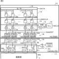
- FIG. 2 is a diagram illustrating an example of the configuration of a horizontal driver according to the embodiment.
- FIG. 3 is a diagram for explaining output of a ramp signal to a signal line.
- FIG. 4 is a timing chart showing the relationship between the ramp waveform and fluctuations in the load current.
- FIG. 5 is a diagram for explaining the installation of the correction current source.
- FIG. 6 is a diagram for explaining the suppression of distortion of the lamp waveform when a correction current source is provided.
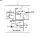
- FIG. 7 is a block diagram illustrating an example of a configuration of a lamp processing unit according to an embodiment.
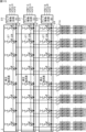
- FIG. 8 is a diagram showing an example of the arrangement of the lamp driving circuit and the correction current supply circuit.
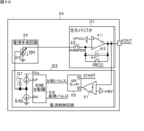
- FIG. 9 is a block diagram showing a specific example of the internal configuration of the ramp generating circuit.
- FIG. 10 is an operation timing diagram of the ramp generating circuit.
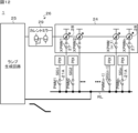
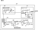
- FIG. 11 is a diagram showing a schematic configuration relating to a correction current of a display device.
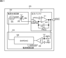
- FIG. 12 is a diagram illustrating an example of a configuration of a display device according to the second embodiment.
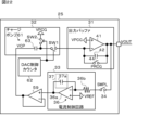
- FIG. 13 is a diagram illustrating an example of a configuration of a display device according to the third embodiment.
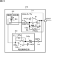
- FIG. 14 is a diagram illustrating an example of a configuration of a display device according to the fourth embodiment.
- FIG. 15 is a diagram illustrating an example of a configuration of a display device according to the fifth embodiment.
- FIG. 16 is a diagram illustrating an example of a configuration of a display device according to the sixth embodiment.
- FIG. 17 is a block diagram showing another example of the configuration of the ramp generating circuit.
- FIG. 18 is a block diagram showing another example of the configuration of the ramp generating circuit.
- FIG. 19 is a block diagram showing another example of the configuration of the ramp generating circuit.
- FIG. 20 is a block diagram showing another example of the configuration of the ramp generating circuit.
- FIG. 21 is a block diagram showing another example of the configuration of the ramp generating circuit.
- FIG. 22 is a block diagram showing another example of the configuration of the ramp generating circuit.
- FIG. 23 is a block diagram showing another example of the configuration of the ramp generating circuit.
- FIG. 24 is a block diagram showing another example of the configuration of the ramp generating circuit.
- FIG. 25 is a block diagram showing another example of the configuration of the ramp generating circuit.
- FIG. 26 is a block diagram showing another example of the configuration of the ramp generating circuit.
- FIG. 27 is a block diagram showing another example of the configuration of the ramp generating circuit.
- FIG. 28 is a block diagram showing an example of the configuration of a vertical driver.
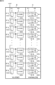
- FIG. 29 is a block diagram showing an example of the configuration of a vertical driver.
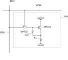
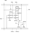
- FIG. 30 is a diagram showing an example of the configuration of a pixel (pixel circuit).
- FIG. 31 is a diagram showing an example of the configuration of a pixel (pixel circuit).
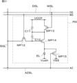
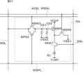
- FIG. 32 is a diagram showing an example of the configuration of a pixel (pixel circuit).
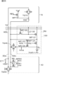
- FIG. 33 is a diagram showing an example of the configuration of a pixel (pixel circuit).
- FIG. 34 is a diagram showing an example of the configuration of a pixel (pixel circuit).
- FIG. 35 is a diagram showing an example of the configuration of a pixel (pixel circuit).
- FIG. 36 is a diagram showing an example of the configuration of a pixel (pixel circuit).
- FIG. 37 is a diagram showing an example of the configuration of a pixel (pixel circuit).
- FIG. 38 is a perspective view showing an example of the appearance of a head mounted display.
- FIG. 39 is a perspective view showing an example of the appearance of a see-through head mounted display.
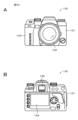
- Fig. 40A is a front view showing an example of the external appearance of a digital still camera
- Fig. 40B is a rear view showing an example of the external appearance of a digital still camera.
- FIG. 40A is a front view showing an example of the external appearance of a digital still camera
- Fig. 40B is a rear view showing an example of the external appearance of a digital still camera.
- FIG. 40A is a front
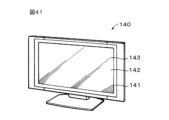
- FIG. 41 is a perspective view showing an example of the appearance of a television device.
- FIG. 42 is a perspective view showing an example of the appearance of a smartphone.
- Fig. 43A is a diagram showing an example of the interior of a vehicle as viewed from the rear to the front of the vehicle
- Fig. 43B is a diagram showing an example of the interior of a vehicle as viewed from diagonally rear to diagonally front of the vehicle.
- Fig. 1 is a block diagram showing a configuration example of a display device according to a first embodiment of the present technology.
- the display device 1 shown in Fig. 1 is a device that displays an image or the like using a light-emitting element.
- the light-emitting element is, for example, an LED (Light Emitting Diode).
- the LED includes an LED used in a micro LED display and an OLED (Organic Light Emitting Diode) used in an organic EL (Electro-Luminescence) display.
- the organic EL display includes, for example, an OLED microdisplay (Organic Light-Emitting Diode Microdisplay).
- the display device 1 will be described as an OLED microdisplay.
- the display device 1 is, for example, a display mounted on an electronic device such as an electronic viewfinder (EVF) of a digital camera, AR glasses, or VR glasses.
- EMF electronic viewfinder
- the electronic devices to which the display device 1 can be applied are not limited to these. Specific configuration examples of electronic devices to which the display device 1 can be applied will be described later.
- the display device 1 has a display panel including a semiconductor substrate such as a silicon substrate. As shown in the figure, the display device 1 has an input/output unit (IO) 2, a gamma processing unit 3, a power supply processing unit 4, an interface unit (IF) 5, a timing controller (TCON) 6, a pixel unit 7, a vertical logic unit (VLOGIC) 8, a vertical analog unit (VANALOG) 9, a horizontal logic unit (HLOGIC) 10, and a horizontal analog unit (HANALOG) 11.
- IO input/output unit
- IF interface unit
- TCON timing controller
- VLOGIC vertical logic unit
- VANALOG vertical analog unit
- HLOGIC horizontal logic unit
- HANALOG horizontal analog unit
- the input/output unit 2 inputs and outputs various data, and is composed of, for example, an externally connectable FPC (Flexible Printed Circuits).
- the input/output unit 2 is connected to the gamma processing unit 3, the power supply processing unit 4, and the interface unit 5.
- the gamma processing unit 3 performs gamma correction processing.
- the gamma processing unit 3 is connected to the input/output unit 2 and the horizontal analog unit 11, and sets gamma correction based on the setting values for gamma correction input via the input/output unit 2, and the pixel signal output from the horizontal analog unit 11 to the pixel unit 7 is gamma corrected.
- the power supply processing unit 4 is a circuit that outputs power supply for driving the pixel unit 7, and is configured to include, for example, an LDO (Low Drop Out) regulator.
- the power supply processing unit 4 is connected to the input/output unit 2 and the pixel unit 7, and converts the supply power input via the input/output unit 2 into a power supply voltage for driving the pixel unit 7 and supplies it to the pixel unit 7.
- the interface unit 5 is connected to the input/output unit 2 and the timing controller 6.
- the interface unit 5 is an interface for inputting and outputting image data, etc., with the outside via the input/output unit 2.
- a high-speed interface standard such as MIPI (Mobile Industry Processor Interface) can be adopted.
- the timing controller 6 controls the timing of each block operation.
- the timing controller 6 is connected to the interface section 5, vertical logic section 8, vertical analog section 9, horizontal logic section 10, and horizontal analog section 11.
- the timing controller 6 outputs control signals to the vertical logic section 8 and vertical analog section 9 as required based on a clock signal.
- the timing controller 6 also outputs image data input via the input/output section 2 and interface section 5 to the horizontal logic section 10 based on the clock signal, and outputs control signals to the horizontal logic section 10 and horizontal analog section 11 as required.
- the pixel section 7 has a plurality of pixels (pixel circuits) arranged in a matrix of m rows and n columns (m and n are natural numbers).
- the pixel section 7 is provided with pixels that represent the three primary colors of R (red), G (green), and B (blue), for example, to represent a color image.
- R red
- G green
- B blue
- the color representation of an image is not limited to this, and may be configured to represent, for example, a monochrome (black and white) image. The configuration and operation of the pixels will be described later.
- the pixel section 7 also has control lines that extend along the rows of the pixel array, and signal lines that extend along the columns of the pixel array.
- a control line is provided for each pixel row, and a signal line is provided for each pixel column.
- the control lines are each connected to the output terminal of the corresponding row of the vertical analog section 9 and the pixel group of the corresponding row.
- the signal lines are each connected to the output terminal of the corresponding column of the horizontal analog section 11 and the pixel group of the corresponding column.
- the vertical logic unit 8 and the vertical analog unit 9 constitute a vertical driver.
- the vertical logic unit 8 generates a shift signal for each pixel row from a start pulse input from the timing controller 6.
- the vertical analog unit 9 generates a control signal that drives a control line from the shift signal and outputs it to the pixel unit 7.
- the horizontal logic unit 10 and the horizontal analog unit 11 constitute a horizontal driver.
- the horizontal logic unit 10 distributes the image data input from the timing controller 6 to each signal line.
- the horizontal analog unit 11 converts the distributed image data into a gamma-corrected pixel signal and outputs it to the corresponding signal line of the pixel unit 7. This technology is particularly characterized by the configuration of the horizontal driver.
- FIG. 2 is a diagram showing a configuration example of a horizontal driver according to the present embodiment.
- the horizontal driver shown in Fig. 2 is configured with a RAMPDAC type circuit that uses a ramp-wave analog signal to generate a pixel signal to be output to a signal line.
- a horizontal logic section 10 constituting this horizontal driver has a shift register section (S/R) 12, a 1ST latch section 13, a 2ND latch section 14, a synchronous counter 15, a DLL (delay-locked loop) circuit 16, a comparator section 17, and a PWM generating section 18.
- S/R shift register section
- 1ST latch section 13 a 1ST latch section 13
- 2ND latch section 14 a synchronous counter
- DLL delay-locked loop
- the 1ST latch unit 13 is composed of the corresponding number of 1ST latch circuits 13A described above, and latches each pixel data input from the shift register unit 12 based on the latch clock LATCLK.
- the 2nd latch unit 14 is composed of the corresponding number of 2nd latch circuits 14A described above, and line-sequentializes each latch data of the 1st latch circuits 13A based on the line pulse LINECLK.
- the synchronous counter 15 receives the main clock signal MCLK from the timing controller 6 via a DLL (delay-locked loop) circuit 16.
- the synchronous counter 15 counts down or up in synchronization with the main clock signal MCLK, and outputs a signal representing the count result.
- the comparator section 17 is composed of a corresponding number of digital comparators 17A as described above. Each digital comparator 17A compares the latch data of each 2nd latch circuit 14A with the output from the synchronous counter 15 and outputs the comparison result.
- the PWM generation section 18 is composed of a corresponding number of PWM generation circuits 18A as described above. Each PWM generation circuit 18A generates a PWM (pulse width) signal according to the gradation data of each pixel in response to the start pulse RAMPST input from the timing controller 6. The generated PWM signal is output to the horizontal analog section 11. As a result, an 8-bit, 10-bit, 12-bit, etc. signal is converted into a signal having a width according to the data and input to the horizontal analog section 11.
- the horizontal analog section 11 constituting the horizontal driver shown in FIG. 2 has a level shifter section 19, a ramp processing section 20, and a switch section 21.
- the level shifter section 19 is composed of the corresponding number of level shifter circuits 19A described above, and converts the level of the PWM signal converted by each PWM generating circuit 18A into a signal of a drive level (voltage level). This signal is used to control the PWM switch 21A in the switch section 21.
- the ramp processing section 20 generates a ramp signal whose voltage level changes over time, and outputs it to the switch section 21 via the ramp wiring RL. In this way, the ramp signal generated by the ramp processing section 20 is supplied to the ramp wiring RL.
- the explanation of the ramp processing section 20 is omitted here, it also serves as a gamma correction circuit, for example, and outputs a ramp wave voltage that has been gamma corrected based on the set value input from the gamma processing section 3.
- the switch section 21 is composed of the corresponding number of PWM switches (first switches) 21A described above.
- Each PWM switch 21A is provided between each signal line SIG connected to a pixel in the pixel section 7 and the lamp wiring RL, and controls the connection between the lamp wiring RL and each corresponding signal line SIG.
- each PWM switch 21A samples the lamp waveform by turning off (closing) at a timing corresponding to the gradation to be written to the pixel according to the output voltage of each level shifter circuit 19A, and determines the signal voltage to be written to the pixel.
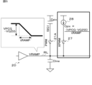
- FIG. 3 is a diagram for explaining the output of a ramp signal to the signal line SIG.
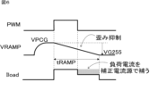
- FIG. 4 is a timing chart showing the relationship between the ramp waveform and the fluctuation of the load current.
- the ramp processing unit 20 of the present embodiment generates and outputs a ramp signal whose voltage level decreases over time.
- FIG. 3 illustrates an example in which the ramp processing unit 20 generates a ramp voltage corresponding to an 8-bit gradation (256 stages of VPCG-VG255) and outputs it as a ramp signal, but as described above, the gradation level may be 10 bits, 12 bits, etc.
- the signal line SIG1 is described as an example, but the same applies to the other signal lines.
- the capacitance on the signal line SIG1 side including the connected pixel (an example of the pixel configuration will be described later), is represented as pixel load capacitance Cpix, and the parasitic capacitance on the lamp wiring RL is represented as wiring load capacitance Cline.
- the load fluctuation caused by the switching of the PWM switch 21A will be described with reference to Fig. 4.
- the pixel load capacitance C load in equation (1) is calculated by equation (2) when the PWM signal that controls the on/off of the PWM switch 21A is high (switched on), and by equation (3) when the PWM signal is low (switched off).
- Cloud Cline+Cpix...(2)
- Cload Cline...(3)
- the ramp voltage VRAMP of the lamp wiring RL of the lamp processing unit 20 is the precharge voltage VPCG, and in this state the PWM signal switches from low to high and the PWM switch 21A turns on. Then, at a timing according to the gradation of the pixel data to be written, the PWM signal goes low and the PWM switch 21A turns off. As a result, a voltage representing the gradation according to the pixel data is written to the pixel.
- the load current Iload fluctuates (decreases in the illustrated example). That is, when the PWM switch 21A is on, the capacitive load Cload is calculated using equation (2), resulting in a high current. On the other hand, when the PWM switch 21A is off, the capacitive load Cload is calculated using equation (3), resulting in a low current, resulting in such a fluctuation in the load current Iload.
- This fluctuation in the load current causes a transient distortion in the ramp voltage VRAMP. For example, if the gate voltage of the current control transistor is controlled by detecting this current fluctuation and applying feedback, the time lag will cause distortion as shown in the figure. This distortion will deteriorate the accuracy of the write voltage. For example, image quality may be affected by horizontal crosstalk caused by the load fluctuation.
- a correction current source 28 is provided in the ramp processing unit 20, and the load current (specifically, the step difference shown in the figure) when the PWM switch 21A is off is compensated for by this correction current source 28.
- the load current Iload during the ramp operation period tRAMP is corrected to maintain a constant state.
- Switching to the correction current source is controlled by an XPWM switch 27 (second switch) that operates inversely to the PWM switch 21A (on/off is reversed).
- the XPWM switch 27 is controlled complementarily to the pixel load.
- FIG. 7 is a block diagram showing an example of the configuration of the lamp processing unit 20 according to this embodiment.
- the lamp processing unit 20 has a correction current supply circuit 24, a lamp generating circuit 25, and a correction current control circuit 26.
- the correction current supply circuit 24 and the correction current control circuit 26 are provided according to the arrangement of the lamp generating circuit 25. First, this arrangement will be described.
- the lamp generating circuit 25 and the correction current control circuit 26 are collectively referred to as the lamp driving circuit 23.
- FIG. 8 is a diagram showing an example of the arrangement of the lamp drive circuit 23 and the correction current supply circuit 24.
- the lamp drive circuit 23 drives each pixel PIX based on a reference voltage VREF and a precharge voltage VPCG.
- an offset voltage VOFS may be used to correct the threshold voltage (Vth) of a drive transistor (DR transistor) that drives a light-emitting element included in the pixel PIX.
- the reference voltage VREF, the precharge voltage VPCG, and the offset voltage VOFS are set voltages that determine the amplitude of the ramp signal, and are used to generate the ramp signal in the ramp generation circuit 25 shown in FIG. 7. Note that this set voltage may be anything that determines the amplitude of the ramp signal, and may include other voltages, for example.
- one lamp drive circuit 23 drives all pixels PIX. All pixels refer to, for example, all pixels that make up the display area. It is to be noted that it may also include pixels outside the display area.
- the current of each correction current source 28 is uniformly controlled by the lamp drive circuit 23. Specifically, there is one lamp generation circuit 25 and one correction current control circuit 26 shown in FIG. 7 for each of all pixels. In addition, there is one correction current supply circuit 24 for each lamp drive circuit 23. Then, the current of each correction current source 28 corresponding to all pixels is collectively controlled using one variable current source 35 of the lamp generation circuit 25 shown in FIG. 7.
- the correction current supply circuit 24 has XPWM switches (second switches) 27 in a number (e.g., n) corresponding to the number of pixel columns provided for each pixel column, and correction current sources 28 in a number (e.g., n) corresponding to the number of pixel columns.
- Each XPWM switch 27 and each correction current source 28 are provided, for example, along the row direction of the pixels PIX.
- the XPWM switch 27 is a complementary switch of the PWM switch 21A. That is, the XPWM switch 27 is turned off when the PWM switch 21A of the corresponding column is turned on, and turned on when the PWM switch 21A of the corresponding column is turned off.
- the PWM switch 21A is turned on/off based on the PWM signal
- the XPWM switch 27 is turned on/off based on the XPWM signal.
- the XPWM signal falls from high level to low level at the timing when the PWM signal rises from low level to high level.
- the XPWM signal rises from low level to high level.
- the PWM switch 21A and the XPWM switch 27 are, for example, composed of transistors.
- the correction current source 28 is a current source that supplies a correction current to the lamp wiring RL.
- Each XPWM switch 27 is provided between the power supply and the corresponding correction current source 28.
- Each correction current source 28 is provided between the corresponding XPWM switch 27 and the lamp wiring RL. Specifically, one end of the XPWM switch 27 is connected to the power supply voltage node, and the other end is connected to the corresponding correction current source 28. The correction current source 28 is connected to the other end of the XPWM switch 27 in the corresponding column, the lamp wiring RL, and the correction current control circuit 26.
- the voltage across both ends of the XPWM switch 27 can be kept unchanged due to complementary operation with the PWM switch 21A and operation with the same amplitude and capacity, and charge scattering (charge scattering to the node) when the XPWM switch 27 is disconnected (off) can be minimized, and writing accuracy can be improved.
- the correction current source 28 passes the correction current generated by the correction current control circuit 26 through the lamp wiring RL when the XPWM switch 27 of the corresponding column is on, that is, when the PWM switch 21A of the corresponding column is off.
- the correction current source 28 is configured, for example, with a transistor diode-connected between the XPWM switch 27 and the lamp wiring RL, or with a circuit that combines the transistor with a resistor.
- the ramp generating circuit 25 includes an output buffer 31, a current generating circuit 32, a current control circuit 33, and an SMPL switch 34.
- the output buffer 31 generates and outputs a ramp wave voltage as a ramp signal.
- the output node (VOUT) of the output buffer 31 is connected to a ramp wiring RL, and one end of each of the PWM switches 21A constituting the switch section 21 described above is connected to the ramp wiring RL.
- the other end of each of the PWM switches 21A is connected to the pixel PIX of the corresponding column via the corresponding signal line SIG.
- the output buffer 31 has an amplifier 41, a load circuit 42, a RAMPEN switch 43, and a PRCG switch 44.
- the amplifier 41 compares the ramp voltage VRAMP with the precharge voltage VPCG and outputs a ramp voltage, which is a comparison result signal.
- the amplifier 41 has a differential amplifier having a first input node to which the precharge voltage VPCG is supplied, a second input node to which a feedback voltage (ramp voltage) is supplied via the load circuit 42, and an output node that outputs a ramp voltage with a voltage level corresponding to the voltage difference between the precharge voltage VPCG and the feedback voltage (ramp voltage).
- this precharge voltage VPCG (VG0) with the offset voltage VOFS so that a ramp signal for correction is generated.
- this can be done by placing a switch (not shown) that switches between VG0 and VOFST in the front stage of the first input node of the output buffer 31 and controlling the switching of this switch. This allows the offset voltage VOFST to be written first and the operation of correcting the threshold voltage of the pixel circuit to be performed.
- the load circuit 42 is disposed on the feedback path of the amplifier 41. More specifically, the load circuit 42 is connected between the second input node and the output node.
- the load circuit 42 includes at least one of a resistive element, a capacitor, and a diode.
- the RAMPEN switch 43 turns on/off based on the logic of the RAMPEN signal.
- the RAMPEN switch 43 is connected between the output node of the current generating circuit 32 and the second input node of the amplifier 41.
- the RAMPEN switch 43 When the RAMPEN switch 43 is turned on, the current output from the current generating circuit 32 flows to the load circuit 42, and the voltage level of the ramp voltage drops.
- the RAMPEN switch 43 When the RAMPEN switch 43 is turned off, no current flows from the current generating circuit 32 to the load circuit 42, and the voltage level of the ramp voltage is maintained.
- the current generating circuit 32 has a variable current source 30 for correction current (described later) and a variable current source 35.
- the variable current source 35 is used to generate a ramp signal.
- the variable current source 35 generates a current based on the set voltages (specifically, VPCG, VREF, VOFS) that set the amplitude of the ramp signal described above.
- the variable current source 35 is a current source whose current value changes according to the amplitude of the ramp signal, that is, the drive amplitude.
- the variable current source 35 is composed of, for example, a transistor diode-connected between the power supply voltage node and the RAMPEN switch 43, or a circuit combining the transistor and a resistor.
- variable current source 35 One end of the variable current source 35 is connected to the power supply voltage node, and the other end is connected to one end of the RAMPEN switch 43 in the output buffer 31.
- the variable current source 35 controls the current flowing to the load circuit 42 based on the comparison result signal output from the current control circuit 33.
- the RAMPEN switch 43 When the RAMPEN switch 43 is turned on, the current from the variable current source 35 flows through the RAMPEN switch 43 to the load circuit 42, and the ramp voltage, which is the output voltage of the output buffer 31, decreases over time.
- the variable current source 30 for correction current is, for example, the same current source as the variable current source 35.
- the variable current source 30 for correction current is a current source whose current value changes according to the amplitude of the ramp signal, that is, the drive amplitude, and generates a current based on a set voltage that sets the amplitude of the ramp signal described above.
- the variable current source 30 for correction current is, for example, a transistor diode-connected between the power supply voltage node and a current mirror section 29 (described later) of the correction current control circuit 26, or a circuit combining the transistor and a resistor.
- variable current source 30 for correction current One end of the variable current source 30 for correction current is connected to the power supply voltage node, and the other end is connected to an input node of the current mirror section 29 of the correction current control circuit 26.
- the variable current source 30 for correction current controls the current flowing to each correction current source 28 based on the comparison result signal output from the current control circuit 33.
- the variable current source 30 for correction current does not necessarily have to be the same current source as the variable current source 35, and may be a current source using the current of the variable current source 35.
- the PRCG switch 44 turns on/off based on the logic of the precharge (PRCG) signal.
- the PRCG switch 44 is connected in parallel to the load circuit 42.
- the PRCG switch 44 turns on for a predetermined period immediately after one horizontal line period starts, and shorts both ends of the load circuit 42, i.e., the second node and the output node of the amplifier 41.
- the current control circuit 33 controls the current generated by the current generation circuit 32 based on the voltage difference between the ramp wave voltage and the reference voltage VREF.
- the current control circuit 33 has a comparator 36 and a holding unit 37.
- the comparator 36 compares the reference voltage VREF with the output voltage (VOUT) of the output buffer 31, and outputs a comparison result signal.
- the holding unit 37 holds the comparison result signal output from the comparator 36.
- the holding unit 37 is composed of, for example, a memory, a voltage holding capacitance, etc.
- the SMPL switch 34 is connected between the output buffer 31 and the comparator 36.
- the SMPL switch 34 turns on/off based on the logic of the SMPL signal.
- the SMPL switch 34 turns on for a predetermined period after the RAMPEN signal transitions from high to low within one horizontal line period.
- the ramp voltage output from the output buffer 31 is input to the comparator 36 via the SMPL switch 34.
- the comparator 36 compares the ramp voltage with the reference voltage VREF only while the SMPL switch 34 is on, and outputs a comparison result signal. While the SMPL switch 34 is off, the holding unit 37 continues to hold the comparison result signal output by the comparator 36 immediately before the SMPL switch 34 was turned on.
- the current generating circuit 32 controls the current flowing to the load circuit 42 in the output buffer 31 based on the comparison result signal held by the holding unit 37. As described above, the current generated by the current generating circuit 32 is supplied to the load circuit 42 only while the RAMPEN switch 43 is on. In addition, the current generating circuit 32 controls the current flowing to each correction current source 28 in the correction current supply circuit 24 based on the comparison result signal held by the holding unit 37.
- FIG. 9 is a block diagram showing a more specific internal configuration of the ramp generating circuit 25 in FIG. 7.
- the ramp generating circuit 25 in FIG. 9 shows a more specific internal configuration of the current control circuit 33 having the comparator 36 and the holding unit 37 in FIG. 7.
- the ramp generating circuit 25 in FIG. 9 also shows an example in which the load circuit 42 in the output buffer 31 has a capacitor.
- the comparator 36 in FIG. 9 has a differential amplifier 36a and a resistive element 36b.
- the differential amplifier 36a has a first input node to which the ramp voltage is input via the SMPL switch 34 and the resistive element 36b, a second input node to which the reference voltage VREF is input, and an output node that outputs a comparison result signal.
- a capacitor 37a functioning as a holding unit 37 is connected between the first input node and the output node of the differential amplifier 36a in FIG. 9.
- the differential amplifier 36a When the SMPL switch 34 is on, the differential amplifier 36a outputs a comparison result signal corresponding to the voltage difference between the ramp wave voltage and the reference voltage VREF from the output node.
- the holding unit 37 holds this comparison result signal in the capacitor 37a while the SMPL switch 34 is off.
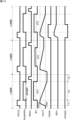
- FIG. 10 is an operation timing diagram of the ramp generating circuit 25 in FIG. 9.
- one horizontal line period has periods T1 to T3.
- the PRCG signal goes high and the PRCG switch 44 turns on. This resets the capacitance of the output buffer 31.
- the second input node and the output node of the amplifier 41 in the output buffer 31 are shorted, and the ramp wave voltage rises to the precharge voltage VPCG.
- This precharge voltage VPCG is, for example, the power supply voltage.
- the RAMPEN signal goes high and the RAMPEN switch 43 turns on. This causes a current (specifically, a constant current) from the variable current source 35 to be applied to the load circuit 42 via the RAMPEN switch 43, and the voltage level of the ramp wave voltage VOUT output from the amplifier 41 decreases over time. During the period when the RAMPEN switch 43 is on, the voltage level of the ramp wave voltage changes over time.
- the RAMPEN signal transitions from high to low when the ramp operation period tRAMP ends and period T3 begins. This turns off the RAMPEN switch 43, the current from the variable current source 35 is no longer applied to the load circuit 42, and the voltage level of the ramp wave voltage becomes constant.
- the output voltage at the start of the ramp operation period tRAMP is VG0, and the output voltage at the end is VG255.
- the output waveform drops from VG0 (VPCG) to VG255 due to the integration of the current flowing through the capacitor 37a.
- This waveform voltage VG255 can be calculated by the following equations (5) and (6).
- the SMPL signal temporarily transitions to a high level.
- the ramp voltage is supplied to the first input node of the differential amplifier 36a in the comparator 36 via the SMPL switch 34.
- the differential amplifier 36a outputs a comparison result signal corresponding to the voltage difference between the ramp voltage and the reference voltage VREF, and holds the comparison result signal in the capacitor 42a.
- the comparison result signal held in the capacitor 42a during the period T3 is used to determine the current flowing from the variable current source 35 during the next horizontal line period.
- the reached potential of the output voltage VOUT is sampled by the current control circuit 33, which functions as a voltage comparison mechanism, and the current of the variable current source 35 of the current generation circuit 32 is controlled.
- this control is performed by modulating the gate potential of the current control transistor of the variable current source 35 with the output signal of the current control circuit 33.
- a ramp waveform is generated in which the voltage reached when current IIN from variable current source 35 is applied for ramp waveform period tFS is the reference voltage VREF.
- the control operates so that it becomes stable when the voltage reached after the ramp operation period tRAMP has elapsed matches the reference voltage VREF.
- the load circuit 42 is placed on the feedback path of the amplifier 41 that outputs the ramp voltage, and the current flowing through the load circuit 42 is variably controlled by the voltage difference between the ramp voltage and the reference voltage VREF.
- the current flowing through the load circuit 42 can be adjusted in accordance with the fluctuations in the ramp voltage due to the coupling capacitance, so that variations in the ramp voltage can be suppressed. Therefore, according to this embodiment, variations in brightness within the display area can be suppressed, improving display quality.
- (Correction current control circuit) 7 is provided between the ramp generating circuit 25 and the correction current supplying circuit 24, and controls the current value of each correction current source 28 based on a current generated based on a set voltage that determines the amplitude of the ramp signal described above. Specifically, the current value of the correction current source 28 is determined based on the variable current source 35 of the ramp generating circuit 25. Specifically, the correction current control circuit 26 has a correction current variable current source 30 of the ramp generating circuit 25 described above, and a current mirror unit 29. The current mirror unit 29 copies (replicates) the reference current generated by the correction current variable current source 30.
- the current mirror unit 29 is configured with a current mirror circuit that receives a current from the current generating circuit 32, and controls the received current to an integer multiple or an integer fraction to create a desired voltage.
- the current mirror unit 29 copies the current of the variable current source 30 for correction current using the current mirror circuit, and supplies a current based on the copied current to the correction current source 28.
- the current mirror circuit has a configuration in which, for example, the gates of two transistors that are diode-connected to the correction current source 28 and the variable current source 30 for correction current are connected to each other, and the collector-base of the transistor on the reference current input side (the variable current source 30 side for correction current) is connected. Note that the configuration of the current mirror circuit is not limited to this, and can be selected appropriately depending on the correction current to be supplied to the lamp wiring RL.
- FIG. 10 the supply operation of the correction current from the correction current source 28 will be described.
- the PWM signal changes from high level to low level
- the corresponding PWM switch 21A is switched from on to off.
- the ramp voltage VRAMP is distorted due to the fluctuation of the load current.
- the XPWM switch 27 and the correction current source 28 as described with reference to FIG. 5, the fluctuation of the load current can be suppressed and the occurrence of distortion of the ramp voltage VRAMP can be suppressed.
- the XPWM signal rises in response to the falling edge of the PWM signal, and the corresponding XPWM switch 27 is switched from off to on, so that the correction current flows in the lamp wiring RL and the distortion is suppressed.
- the falling and rising timings of the XPWM signal are the same as the rising and falling timings of the PWM signal, as shown in FIG. 10.
- the rising timing of the XPWM signal may be shifted within a range in which the distortion suppression effect occurs within the period in which the ramp waveform is operating (specifically, the ramp waveform period tFS).
- the period in which both the PWM switch 11A and the XPWM switch 27 are on or both are off may be included.
- the current of the correction current source 28 is controlled so that the amplitude of the ramp signal becomes the set voltage, which improves the correction accuracy. Since the current value of the correction current source 28 is determined based on the variable current source 35 for generating the ramp signal, distortion can be suppressed with a simple configuration.
- the ramp generating circuit 25 passes a current through the load circuit 42 attached to the feedback path of the output buffer 31 to generate a ramp signal having a ramp waveform. Then, the correction current control circuit 26 copies a current based on this applied current. Then, each correction current source 28 applies a correction current based on this copied current to the ramp wiring RL from the timing when the pixel load is closed, thereby suppressing load fluctuations as seen from the output buffer 31. In other words, it is possible to appropriately suppress waveform distortion when the load is disconnected. In this way, by utilizing the configuration of the ramp generating circuit 25 already provided in the display device 1, it is possible to suppress pixel load fluctuations with a simple configuration.
- the XPWM switch 27 is turned off when the PWM switch 11A is on during the entire period, and turned on when the PWM switch 11A is off.
- the operation example is not limited to this.
- the XPWM switch 27 may be turned on only during the period during which the ramp waveform is operating, during which the above-mentioned distortion may occur.
- the timing at which the PWM signal rises from a low level to a high level outside the ramp waveform operation period and the timing at which the XPWM signal falls from a high level to a low level may or may not match.
- the XPWM switch 27 may be turned off or on outside the ramp waveform operation period. When the XPWM switch 27 is turned off outside the ramp waveform operation period, unnecessary load current can be reduced.
- each XPWM switch 27 is provided between the power supply and the corresponding correction current source 28, and each correction current source 28 is provided between the corresponding XPWM switch 27 and the lamp wiring RL. That is, the connection from the power supply voltage node to the lamp wiring RL in the correction current supply circuit 24 is in the order of power supply voltage node ⁇ XPWM switch 27 ⁇ correction current source 28 ⁇ lamp wiring RL. However, this order can be changed.
- connection path to the lamp wiring RL in the correction current supply circuit 24 is arranged in the order of power supply ⁇ correction current source 28 ⁇ XPWM switch 27. That is, the correction current source 28 is provided between the power supply and the XPWM switch 27, and the XPWM switch 27 is provided between the correction current source 28 and the lamp wiring RL.
- This configuration can also achieve the same effects as the first embodiment described above.
- the arrangement is the same as that of the PWM switch 21A connected to the pixel load side, so that the XPWM switch 27 operates complementarily with the PWM switch 21A, thereby canceling signal feedthrough (for example, charge inflow phenomenon through the capacitance between the gate and source and between the gate and drain due to fluctuations in the switch control signal when the switch is configured with a transistor).
- signal feedthrough for example, charge inflow phenomenon through the capacitance between the gate and source and between the gate and drain due to fluctuations in the switch control signal when the switch is configured with a transistor.
- the above-mentioned correction current source 28 is positioned according to the lamp operation direction associated with the waveform of the ramp signal supplied to the ramp wiring RL.
- the ramp signal has a ramp waveform in which the voltage level decreases over time. That is, the correction current source 28 is provided on the power supply side so as to correspond to a ramp waveform that operates from the high voltage side to the low voltage side.
- the ramp signal is not limited to this.
- FIG. 13 shows an example of the configuration of a display device 1 according to the third embodiment.
- the waveform of the ramp signal generated by the ramp generating circuit 25 differs from that described in the first embodiment.
- the ramp generating circuit 25 of this display device 1 has a configuration for generating a ramp signal having a ramp waveform that increases over time, and outputs the generated ramp signal to the ramp wiring RL.
- the connection path to the lamp wiring RL in the correction current supply circuit 24 is formed by arranging the ground ⁇ XPWM switch 27 ⁇ correction current source 28 in that order.
- the XPWM switch 27 is provided between the ground (GND) and the correction current source 28.
- the correction current source 28 is provided between the XPWM switch 27 and the lamp wiring RL.
- one end of the XPWM switch 27 is connected to the ground node.
- FIG. 14 shows a configuration example of the display device 1 according to the fourth embodiment.
- the ramp generating circuit 25 of the display device 1 shown in FIG. 14 has a configuration for generating a ramp signal having a ramp waveform that increases with time, similar to the third embodiment.
- a connection path to the ramp wiring RL in the correction current supply circuit 24 is formed by arranging the ground ⁇ correction current source 28 ⁇ XPWM switch 27 in this order. That is, the XPWM switch 27 is provided between the correction current source 28 and the ramp wiring RL.
- the correction current source 28 is provided between the ground and the XPWM switch 27. Specifically, one end of the correction current source 28 is connected to the ground node.
- This configuration can also achieve the same effects as the first embodiment described above.
- the signal waveform of the ramp signal supplied to the lamp wiring RL is not limited to those shown in Figures 11 to 14.
- it may be a triangular wave, a V-shaped wave, a sawtooth wave, etc.
- the slope of the waveform is not limited to being linear but may be stepped.
- it is not limited to being a waveform that changes regularly over time but may be a waveform that changes irregularly.
- it may have a waveform that is a combination of these.
- various ramp signals that change over time can be adopted for use in the display device 1.
- a correction current source 28 and an XPWM switch 27 it is possible to adapt it by arranging a correction current source 28 and an XPWM switch 27 on both the power supply side and the ground side and switching to the corresponding one depending on the output waveform.
- the display device 1 of the first embodiment described above has a configuration in which one lamp drive circuit 23 and one correction current supply circuit 24 are provided for all pixels PIX, but the arrangement of the lamp drive circuit 23 and the correction current supply circuit 24 is not limited to this. The same applies to the first to fourth embodiments described above.
- FIG. 15 is a diagram showing an example of the configuration of a display device 1 according to a fifth embodiment.
- the display device 1 of this embodiment has a ramp generation circuit 25 for each pixel color, and uses a variable current source 35 corresponding to the color used in each ramp generation circuit 25 to control the current of each correction current source 28 according to the color of the corresponding pixel PIX.
- this display device 1 is provided with lamp drive circuits 23 and correction current supply circuits 24 for each color of sub-pixels, which are divided into R (red) pixel PIX, G (green) pixel PIX, and B (blue) pixel PIX.
- the R lamp drive circuit 23 receives an R reference voltage VREF_R, an R precharge voltage VPCG_R, and an offset voltage VOFS to generate a correction current for R, and outputs the generated correction current from the R correction current supply circuit 24 to the R lamp wiring RL to drive the R pixel PIX.
- the G lamp drive circuit 23 receives a G reference voltage VREF_G, a G precharge voltage VPCG_G, and an offset voltage VOFS to generate a G correction current, and outputs the generated correction current from the G correction current supply circuit 24 to the G lamp wiring RL to drive the G pixel PIX.
- the B lamp drive circuit 23 receives the B reference voltage VREF_B, the B precharge voltage VPCG_B, and the offset voltage VOFS to generate a B correction current, which is then output from the B correction current supply circuit 24 to the B lamp wiring RL to drive the B pixel PIX.
- the colors of the sub-pixels are not limited to the three colors R, G, and B, and may include, for example, W (white).
- Sixth embodiment 16 is a diagram showing an example of the configuration of a display device 1 according to a sixth embodiment.
- the display device 1 of this embodiment has a ramp generating circuit 25 for each block consisting of a predetermined number of pixels, and controls the current of each correction current source 28 on a block-by-block basis using a variable current source 35 used in each ramp generating circuit 25.
- this display device 1 has lamp drive circuits 23 and correction current supply circuits 24 arranged every predetermined number of pixel columns (for example, several tens of pixel columns or several hundred pixel columns). For example, when arranged every 10 pixel columns, one block contains 10 x m pixels PIX.
- the reference bias is determined for each circuit of each block, so that the influence of IR drop of the power supply (or ground if the correction current source 28 is connected to the ground side) can be mitigated.
- this predetermined number may be arranged in a regular or irregular manner as multiple types.
- the blocks may not only be arranged along the row direction as shown in FIG. 16, but may also be arranged along the column direction or may be distributed. In this way, the arrangement of the lamp drive circuit 23 and the correction current supply circuit 24 is not limited to that shown in FIG. 8, and can be appropriately set with respect to the arrangement of the pixels PIX.
- Fig. 17 is a block diagram showing another example of the configuration of the ramp generating circuit 25.
- the ramp generating circuit 25 in Fig. 17 generates a ramp voltage whose voltage level increases with time.
- This ramp generating circuit 25 differs from the ramp generating circuit 25 shown in Fig. 9 in the configuration of the current generating circuit 32.
- one end of the variable current source 35 is connected to the ground node, and the other end is connected to one end of the RAMPEN switch 43 of the output buffer 31.
- the other configuration is the same as that in Fig. 9.
- the ramp generation circuit 25 operates, for example, as follows. When one horizontal line period begins, the PRCG switch 44 turns on and the ramp voltage drops to the precharge voltage VPCG (for example, the ground voltage). Next, the PRCG switch 44 turns off and the RAMPEN switch 43 turns on, causing a current to flow from the load circuit 42 through the RAMPEN switch 43 to the variable current source 35, causing the ramp voltage, which is the output voltage of the output buffer 31, to rise over time.
- VPCG for example, the ground voltage
- the SMPL switch 34 is turned on, and the ramp voltage is supplied to the first input node of the differential amplifier 36a via the SMPL switch 34.
- the differential amplifier 36a outputs a comparison result signal corresponding to the voltage difference between the ramp voltage and the reference voltage VREF, and holds the comparison result signal in the capacitor 37a. This held comparison result signal is used to determine the current flowing from the variable current source 35 during the next horizontal line period. This series of operations is repeated in the same manner during the next horizontal line period.
- variable current source 30 for correction current may have one end connected to the ground node, similar to the variable current source 35.
- Fig. 18 is a block diagram showing another example of the configuration of the ramp generating circuit 25.
- the ramp generating circuit 25 shown in Fig. 18 generates a ramp voltage having a triangular waveform.
- This ramp generating circuit 25 differs from the ramp generating circuit 25 shown in Fig. 9 in the configuration of the output buffer 31 and the current generating circuit 32.
- the output buffer 31 in Fig. 18 has a first RAMPEN switch 43a that is turned on/off in response to a RAMPEN1 signal and a second RAMPEN switch 43b that is turned on/off in response to a RAMPEN2 signal, instead of the RAMPEN switch 43 in Fig. 9.
- the current generating circuit 32 in FIG. 18 has a first variable current source 35a and a second variable current source 35b as variable current sources 35, and a bias circuit 38.
- One end of the first variable current source 35a is connected to a power supply voltage node, and the other end is connected to one end of the first RAMPEN switch 43a.
- One end of the second variable current source 35b is connected to a ground node, and the other end is connected to one end of the second RAMPEN switch 43b.
- the other end of the first RAMPEN switch 43a and the other end of the second RAMPEN switch 43b are connected to the load circuit 42 and the second input node of the amplifier 41.
- the bias circuit 38 controls the current flowing through the first variable current source 35a and the second variable current source 35b based on the comparison result signal held in the holding unit 37.
- the ramp generation circuit 25 operates, for example, as follows. At the start of one horizontal line, the first RAMPEN switch 43a and the second RAMPEN switch 43b are both off. In this state, the PRCG switch 44 turns on and the ramp voltage rises to the precharge voltage. Next, the first RAMPEN switch 43a turns on, and current flows from the first variable current source 35a to the load circuit 42 via the first RAMPEN switch 43a, and the ramp voltage, which is the output voltage of the output buffer 31, decreases over time. After that, the SMPL switch 34 turns on temporarily after a period of tFS/2 has elapsed, and the comparator 36 outputs a comparison result signal between the ramp voltage at that time and the reference voltage VREF, and the holding unit 37 holds this comparison result signal.
- the first RAMPEN switch 43a is turned off and the second RAMPEN switch 43b is turned on. This causes current to flow from the load circuit 42 to the second variable current source 35b via the second RAMPEN switch 43b, and the ramp voltage, which is the output voltage of the output buffer 31, increases over time. After that, the first RAMPEN switch 43a and the second RAMPEN switch 43b are both turned off, and the ramp voltage, which is the output voltage of the output buffer 31, maintains the precharge voltage VPCG.
- variable current source 30 for correction current may be provided with a current source corresponding to the first variable current source 35a, a current source corresponding to the second variable current source 35b, and a changeover switch, and the changeover switch may be configured to select the current source corresponding to the one controlling the current flowing through the load circuit 42.
- Fig. 19 is a block diagram showing another example of the configuration of the ramp generation circuit 25.
- the ramp generation circuit 25 shown in Fig. 19 is different from the ramp generation circuit 25 shown in Fig. 9 in the configuration of the current control circuit 33, but the other configurations are similar.
- the current control circuit 33 in Fig. 19 has a digital comparator 51, an SR latch 52, a phase comparator 53, a first current source 54a, a second current source 54b, and a holding unit 37.
- the digital comparator 51 compares the ramp voltage, which is the output voltage of the output buffer 31, with the reference voltage VREF, and outputs a binary signal, which is a comparison result signal. For example, when the ramp voltage becomes less than the reference voltage VREF, the digital comparator 51 outputs a high-level comparison result signal.
- the SR latch 52 is set and the output becomes high level, and when the comparison result signal of the digital comparator 51 becomes high level, the SR latch 52 is reset and the output becomes low level.
- the output signal of the SR latch 52 is referred to as a comparison pulse signal.
- the phase comparator 53 outputs an UP signal or a DOWN signal depending on the phase difference between the comparison pulse signal output from the SR latch 52 and the reference pulse signal.
- the first current source 54a passes a current while the UP signal is at a high level, charging the capacitor that constitutes the holding unit 37.
- the second current source 54b discharges this capacitor while the DOWN signal is at a high level, passing the discharge current to the ground node.
- the ramp generating circuit 25 operates, for example, as follows. If the comparison pulse signal output from the SR latch 52 falls later than the reference pulse signal, the ramp voltage is too high, and the phase comparator 53 sets the DOWN signal to high level. Therefore, the variable current source 35 controls the load circuit 42 so that more current flows, and the voltage level of the ramp voltage is further reduced. If the comparison pulse signal falls earlier than the reference pulse signal, the ramp voltage is too low, and the phase comparator 53 sets the UP signal to high level. Therefore, the variable current source 35 controls the load circuit 42 so that less current flows, and the voltage level of the ramp voltage is further increased. If the phases of the comparison pulse signal and the reference pulse signal are the same, the phase comparator 53 sets both the UP signal and the DOWN signal to low level. Therefore, the variable current source 35 passes a current corresponding to the comparison result signal held in the holding unit 37 to the load circuit 42.
- the current control circuit 33 that controls the current of the variable current source 35 can be configured using a phase comparator 53, making integration easier and achieving a smaller area and lower power consumption.
- Fig. 20 is a block diagram showing another example of the configuration of the ramp generating circuit 25.
- the ramp generating circuit 25 shown in Fig. 20 differs from the ramp generating circuit 25 shown in Fig. 9 in the configurations of the current generating circuit 32 and the current control circuit 33, but the other configurations are similar.
- the current generating circuit 32 in Fig. 20 has a variable current source 35 and a DA converter (hereinafter, DAC) 55.
- the variable current source 35 generates a current according to a current control signal output from the DAC 55.
- the current control circuit 33 in FIG. 20 has a digital comparator 51, an SR latch 52, a pulse counter 56, a holding unit 37, and an arithmetic circuit 57.
- the digital comparator 51 and the SR latch 52 are the same as those in the current control circuit 33 in FIG. 19, and the SR latch 52 outputs a comparison pulse signal.
- the pulse counter 56 counts the pulse width of the comparison pulse signal output from the SR latch 52 using the clock signal CLK, and outputs the count value.
- the holding unit 37 holds the count value output from the pulse counter 56.
- the holding unit 37 holds the count value, for example, in a flip-flop. Alternatively, the holding unit 37 may hold the count value in a plurality of logic gates.
- the arithmetic circuit 57 generates a digital current control signal for controlling the current of the variable current source 35 based on the count value.
- the DAC 55 of the current generation circuit 32 generates a current control signal by DA converting the digital current control signal.
- variable current source 30 for correction current may generate a current according to the current control signal output from the DAC 55, similar to the variable current source 35.
- Fig. 21 is a block diagram showing another example of the configuration of the ramp generation circuit 25.
- the ramp generation circuit 25 shown in Fig. 21 differs from the ramp generation circuit 25 shown in Fig. 20 in the configuration of the current control circuit 33, but the other configurations are similar.
- the current control circuit 33 in Fig. 20 has a comparator 36 and a successive approximation register analog-to-digital converter (hereinafter, SAR ADC: Successive Approximation Register Analog Digital Converter) 58.
- SAR ADC Successive Approximation Register Analog Digital Converter
- the comparator 36 outputs a comparison result signal according to the potential difference between the ramp voltage, which is the output voltage of the output buffer 31, and the reference voltage VREF.
- the SAR ADC 58 performs successive comparison processing on the comparison result signal output from the comparator 36, and outputs a digital signal according to the comparison result signal.
- the DAC 55 in the current generation circuit 32 converts the digital signal output from the SAR ADC 58 into an analog current control signal.
- the variable current source 35 controls the current flowing through the load circuit 42 based on the current control signal.
- the SAR ADC 58 performs AD conversion processing when the SMPL switch 34 is on, and when the SMPL switch 34 transitions from on to off, it holds the digital signal immediately before that.
- Fig. 22 is a block diagram showing another example of the configuration of the ramp generating circuit 25.
- the variable current source 35 is used in the current generating circuit 32, but it is not necessary to use the variable current source 35.
- the ramp generating circuit 25 shown in Fig. 22 has an output buffer 31 (however, the RAMPEN switch 43 is not necessary) having the same configuration as in Fig. 9, a comparator 36, and a holding unit 37.
- a voltage follower circuit 59 is connected to the output of the comparator 36.
- the current generating circuit 32 in FIG. 22 has a charge pump 61 provided in place of the variable current source 35, and a DAC control counter 62.
- the charge pump 61 has a capacitor 63 and a switch SW1 connected in series between the output node of the voltage follower circuit 59 and the second input node of the amplifier 41 in the output buffer 31, and a switch SW2 connected between the connection node of the capacitor 63 and the switch SW1 and the precharge voltage VPCG node.
- the DAC control counter 62 performs a counting operation at a predetermined time interval.
- the predetermined time interval is the time interval at which the ramp voltage is updated.
- the comparator 36 in the current control circuit 33 compares the ramp voltage with the reference voltage VREF for each horizontal line period, and inputs a voltage signal according to the comparison result signal to the charge pump 61.
- the switches SW1 and SW2 in the charge pump 61 are temporarily turned on each time the DAC control counter 62 counts up.
- the cycle in which the DAC control counter 62 counts up is much shorter than one horizontal line period.
- the charge pump 61 can stepwise switch the current flowing to the load circuit 42 by repeatedly turning on the switches SW1 and SW2 temporarily. This causes the voltage level of the ramp voltage to decrease stepwise (in a staircase pattern).
- the charge pump 61 can be used as the variable current source 30 for correction current.
- the variable current source 35 described above can be configured with the charge pump 61, and a current source based on the current of the charge pump 61 can be used as the variable current source 30 for correction current.
- Fig. 23 is a block diagram showing another example of the configuration of the ramp generating circuit 25.
- the ramp generating circuit 25 in Fig. 23 differs from the ramp generating circuit 25 shown in Fig. 9 in the configuration of the load circuit 42 of the output buffer 31.
- the other configurations are similar.
- the load circuit 42 of the output buffer 31 has a resistor element 42b and a capacitor 42a connected in series between the second input node and the output node of the amplifier 41.
- the load circuit 42 were composed only of a capacitor as in FIG. 9, there is a risk that the waveform of the ramp voltage would change nonlinearly when the voltage level of the ramp voltage begins to drop.
- the load circuit 42 in FIG. 23 has a resistive element 42b connected in series with the capacitor 42a, and therefore the voltage level can be changed almost linearly when the ramp voltage begins to drop. This makes it possible to reduce errors in the signal line voltage when the signal line voltage is determined using the ramp voltage.
- Fig. 24 is a block diagram showing another example of the configuration of the ramp generating circuit 25.
- the ramp generating circuit 25 in Fig. 24 has a current generating circuit 32 and a current control circuit 33 having the same configuration as in Fig. 9.
- the output buffer 31 in Fig. 24 has a load circuit 42 having a circuit configuration different from that shown in Fig. 23.
- the load circuit 42 in Fig. 24 is composed of a variable resistor 42c.
- the resistance value of the variable resistor is controlled in stages by the DAC control counter 62. More specifically, the resistance value of the variable resistor increases in stages as the count value of the DAC control counter 62 increases. As a result, the ramp voltage decreases in stages (in a step-like manner) from the precharge voltage.
- Fig. 25 is a block diagram showing another example of the configuration of the ramp generation circuit 25.
- the ramp generation circuit 25 in Fig. 25 has an output buffer 31 and a current control circuit 33 having the same configuration as in Fig. 9.
- the current generation circuit 32 in Fig. 25 has a current DAC 66 including x current sources 64 (x is an integer of 2 or more) that each pass a different current, and x switches 65.
- the corresponding current sources 64 and switches 65 are connected in series.
- Each current source 64 and each switch 65 corresponds to each bit of the x-bit count value output from the DAC control counter 62.
- the most significant bit of the count value corresponds to the leftmost current source 64 and switch 65, and the least significant bit of the count value corresponds to the rightmost current source 64 and switch 65.
- the x current sources 64 variably control the current IIN in response to a comparison result signal output from the comparator 36 in the current control circuit 33.
- the leftmost current source 64 passes a current of 2 x ⁇ IIN
- the adjacent current source 64 passes a current of 2 x-1 ⁇ IIN
- the second current source 64 from the rightmost passes a current of 2 ⁇ IIN
- the rightmost current source 64 passes a current of IIN.
- the currents flowing through the x current sources 64 and the x switches 65 are added together and supplied to the load circuit 42.
- this current DAC 66 can be used as the variable current source 30 for correction current.
- the above-mentioned variable current source 35 can be configured with this current DAC 66, and a current source based on the current of this current DAC 66 can be used as the variable current source 30 for correction current. The same applies to the next configuration example 10.
- Fig. 26 is a block diagram showing another example of the configuration of the ramp generating circuit 25.
- the ramp generating circuit 25 in Fig. 26 has a current generating circuit 32 and a current control circuit 33 having the same configuration as in Fig. 25.
- the load circuit 42 of the output buffer 31 in Fig. 26 has a diode instead of a resistive element. Since the relationship between the forward voltage and the forward current of a diode is nonlinear, the ramp voltage has a nonlinear waveform.
- the load circuit 42 may be configured with a diode connected in series to a resistive element. This allows the nonlinear shape of the ramp voltage to approach a linear shape.
- (Other Configuration Example 11) 27 is a block diagram showing another example of the configuration of the ramp generating circuit 25.
- the ramp generating circuit 25 in FIG. 27 includes an output buffer 31 and a current generating circuit 32 having the same configuration as in FIG. 21.
- the ramp generating circuit 25 in FIG. 27 includes a setting and holding register 69 instead of the current control circuit 33.
- the ramp voltage which is the output voltage of the output buffer 31, is monitored, and the current to be passed through the load circuit 42 and the control value of the variable current source 35 for passing that current are detected in advance. Then, the display device 1 is shipped after storing that control value in the setting and holding register 69.
- the current generating circuit 32 passes a current from the variable current source 35 to the load circuit 42 based on a control signal obtained by DA-converting the control value stored in the setting and holding register 69 by the DAC 55, and adjusts the voltage level of the ramp voltage.
- Example of Vertical Driver Configuration 28 is a block diagram showing a configuration example (first configuration example) of a vertical driver.
- the vertical driver can be configured, for example, by a shift register type circuit having a shift register circuit in a signal input section.
- a vertical logic section 8 constituting this vertical driver has a shift register section 81 and a logic circuit section 82.
- a vertical analog section 9 has a level shifter section 91 and an output buffer section 92.
- the shift register section 81 is composed of shift registers 81A, the number of which corresponds to the number m of pixels in the column direction (for example, m), and the start pulse VST is synchronized with the clock signal CLK, propagates in sequence, and is output row by row in sequence as shift signals SR0, SR1, ....
- the logic circuit section 82 is composed of the corresponding number of logic circuits (LOGIC) 82A described above, and performs logical operations as necessary in response to an input control signal (not shown).
- the level shifter section 91 is composed of the corresponding number of level shifters 91A described above, and converts the levels of the signals SR0, SR1, ... that have been subjected to logical operations into drive level signals (control signals).
- the output buffer section 92 is composed of the corresponding number of buffer circuits 92A described above, and buffers and outputs the control signals.
- FIG. 29 is a block diagram showing a configuration example (second configuration example) of a vertical driver.
- This vertical driver has an address decoder 83 instead of the shift register section 81 of the vertical driver shown in FIG. 28.
- the vertical driver can be configured, for example, with an address decoder type circuit having an address decoder 83 in the signal input section.
- the other configuration is the same as the vertical driver in FIG. 28.
- the address decoder 83 decodes the address based on the address information COUNT supplied from the timing controller 6, and outputs the decoded result in correspondence with the logic circuit 82A of each row.
- the shift register section 81 described above is configured to always shift in a specific order, such as from top to bottom or bottom to top, but the address decoder 83 can sequentially specify and scan between specific addresses, such as incrementing from an arbitrary address to a certain address.
- the configuration of the vertical driver is not limited to that shown in Figures 28 and 29, and can be modified as appropriate according to the pixel configuration, operation, etc.
- Example of pixel circuit configuration (First Configuration Example) 30 shows an example of the configuration of a pixel PIX.
- the pixel PIX has a capacitor C01, transistors MN02 and MN03, and a light-emitting element EL.
- the transistors MN02 and MN03 are N-type MOSFETs (Metal Oxide Semiconductor Field Effect Transistors).
- the gate of the transistor MN02 is connected to a control line WSL, the drain is connected to a signal line SGL, and the source is connected to the gate of the transistor MN03 and the capacitor C01.
- One end of the capacitor C01 is connected to the source of the transistor MN02 and the gate of the transistor MN03, and the other end is connected to the source of the transistor MN03 and the anode of the light-emitting element EL.
- the gate of the transistor MN03 is connected to the source of the transistor MN02 and one end of the capacitor C01, the drain is connected to the power supply line VCCP, and the source is connected to the other end of the capacitor C01 and the anode of the light-emitting element EL.
- the anode of the light-emitting element EL is connected to the source of the transistor MN03 and the other end of the capacitor C01, and the cathode is connected to the power supply line Vcath.
- the voltage of the power supply line VCCP is appropriately switched between a first voltage and a second voltage lower than the first voltage.
- pixel PIX when transistor MN02 is turned on, the voltage across capacitor C01 is set based on the pixel signal supplied from signal line SGL.
- transistor MN03 passes a current corresponding to the voltage across capacitor C01 through light-emitting element EL.
- the light-emitting element EL emits light based on the current supplied from transistor MN03.
- pixel PIX emits light with a brightness corresponding to the pixel signal. Note that during the period when the voltage of power line VCCP is the second voltage, the light-emitting element EL is turned off.
- (Second Configuration Example) 31 shows an example of the configuration of a pixel PIX.
- This pixel PIX has capacitors C11 and C12, transistors MP12 to MP15, and a light-emitting element EL.
- the transistors MP12 to MP15 are P-type MOSFETs.
- the gate of the transistor MP12 is connected to a control line WSL, the source is connected to a signal line SGL, and the drain is connected to the gate of the transistor MP14 and the capacitor C12.
- One end of the capacitor C11 is connected to a power supply line VCCP, and the other end is connected to the capacitor C12, the drain of the transistor MP13, and the source of the transistor MP14.
- One end of the capacitor C12 is connected to the other end of the capacitor C11, the drain of the transistor MP13, and the source of the transistor MP14, and the other end is connected to the drain of the transistor MP12 and the gate of the transistor MP14.
- the gate of the transistor MP13 is connected to the control line DSL, the source is connected to the power supply line VCCP, and the drain is connected to the source of the transistor MP14, the other end of the capacitor C11, and one end of the capacitor C12.
- the gate of the transistor MP14 is connected to the drain of the transistor MP12 and the other end of the capacitor C12, the source is connected to the drain of the transistor MP13, the other end of the capacitor C11, and one end of the capacitor C12, and the drain is connected to the anode of the light-emitting element EL and the source of the transistor MP15.
- the gate of the transistor MP15 is connected to the control line AZSL, the source is connected to the drain of the transistor MP14 and the anode of the light-emitting element EL, and the drain is connected to the power supply line VSS.
- Transistor MP13 when transistor MP12 is turned on, the voltage across capacitor C12 is set based on the pixel signal supplied from signal line SGL.
- Transistor MP13 turns on and off based on the signal on control line DSL.
- transistor MP14 passes a current corresponding to the voltage across capacitor C12 through light-emitting element EL.
- Light-emitting element EL emits light based on the current supplied from transistor MP14. In this way, pixel PIX emits light at a brightness corresponding to the pixel signal.
- Transistor MP15 turns on and off based on the signal on control line AZSL. During the period when transistor MP15 is on, the voltage of the anode of light-emitting element EL is initialized by being set to the voltage of power supply line VSS.
- transistors MP12 to MP15 may be transistors using low temperature polycrystalline silicon (LTPS).
- at least one of transistors MP12 and MP15 may be a transistor using an oxide semiconductor.
- (Third Configuration Example) 32 shows an example of the configuration of a pixel PIX.
- This pixel PIX has a capacitor C21, transistors MN22 to MN25, and a light-emitting element EL.
- the transistors MN22 to MN25 are N-type MOSFETs.
- the gate of the transistor MN22 is connected to a control line WSL, the drain is connected to a signal line SGL, and the source is connected to the gate of the transistor MN24 and the capacitor C21.
- One end of the capacitor C21 is connected to the source of the transistor MN22 and the gate of the transistor MN24, and the other end is connected to the source of the transistor MN24, the drain of the transistor MN25, and the anode of the light-emitting element EL.
- the gate of the transistor MN23 is connected to a control line DSL, the drain is connected to a power supply line VCCP, and the source is connected to the drain of the transistor MN24.
- the gate of transistor MN24 is connected to the source of transistor MN22 and one end of capacitor C21, the drain is connected to the source of transistor MN23, the source is connected to the other end of capacitor C21, the drain of transistor MN25, and the anode of the light-emitting element EL.
- the gate of transistor MN25 is connected to control line AZSL, the drain is connected to the source of transistor MN24, the other end of capacitor C21, and the anode of the light-emitting element EL, and the source is connected to the power supply line VSS.
- Transistor MN23 when transistor MN22 is turned on, the voltage across capacitor C21 is set based on the pixel signal supplied from signal line SGL.
- Transistor MN23 turns on and off based on the signal on control line DSL.
- transistor MN24 passes a current corresponding to the voltage across capacitor C21 through light-emitting element EL.
- Light-emitting element EL emits light based on the current supplied from transistor MN24. In this way, pixel PIX emits light with a brightness corresponding to the pixel signal.
- Transistor MN25 turns on and off based on the signal on control line AZSL. During the period when transistor MN25 is on, the voltage of the anode of light-emitting element EL is initialized by being set to the voltage of power supply line VSS.
- the transistors MN22 to MN25 may be transistors using low temperature polycrystalline silicon (LTPS).
- at least one of the transistors MN22 and MN25 may be a transistor using an oxide semiconductor.
- FIG. 33 shows an example of the configuration of a pixel PIX.
- This pixel PIX has a capacitor C31, transistors MP32 to MP36, and a light-emitting element EL.
- the transistors MP32 to MP36 are P-type MOSFETs.
- the gate of the transistor MP32 is connected to a control line WSL, the source is connected to a signal line SGL, and the drain is connected to the gate of the transistor MP33, the drain of the transistor MP34, and the capacitor C31.
- One end of the capacitor C31 is connected to a power supply line VCCP, and the other end is connected to the drain of the transistor MP32, the gate of the transistor MP33, and the drain of the transistor MP34.
- the gate of the transistor MP34 is connected to a control line AZSL1, the source is connected to the drain of the transistor MP33 and the source of the transistor MP35, and the drain is connected to the drain of the transistor MP32, the gate of the transistor MP33, and the other end of the capacitor C31.
- the gate of the transistor MP35 is connected to the control line DSL, the source is connected to the drain of the transistor MP33 and the source of the transistor MP34, the drain is connected to the source of the transistor MP36 and the anode of the light-emitting element EL.
- the gate of the transistor MP36 is connected to the control line AZSL2, the source is connected to the drain of the transistor MP35 and the anode of the light-emitting element EL, and the drain is connected to the power supply line VSS.
- Transistor MP35 when transistor MP32 is turned on, the voltage across capacitor C31 is set based on the pixel signal supplied from signal line SGL. Transistor MP35 is turned on and off based on the signal on control line DSL. During the period when transistor MP35 is on, transistor MP33 passes a current corresponding to the voltage across capacitor C31 through light-emitting element EL. Light-emitting element EL emits light based on the current supplied from transistor MP33. In this way, pixel PIX emits light with a luminance corresponding to the pixel signal. Transistor MP34 is turned on and off based on the signal on control line AZSL1.
- Transistor MP36 is turned on and off based on the signal on control line AZSL2.
- the voltage of the anode of light-emitting element EL is initialized by being set to the voltage of power supply line VSS.
- transistors MP32 to MP36 may be transistors using low temperature polycrystalline silicon (LTPS). Also, at least one of transistors MP32, MP34, and MP36 may be a transistor using an oxide semiconductor.
- LTPS low temperature polycrystalline silicon
- (Fifth Configuration Example) 34 shows an example of the configuration of pixel PIX.
- One end of capacitor C48 is connected to signal line SGL1, and the other end is connected to power supply line VSS.
- One end of capacitor C49 is connected to signal line SGL1, and the other end is connected to signal line SGL2.
- Transistor MP49 is a P-type MOSFET, with its gate connected to control line WSL2, its source connected to signal line SGL1, and its drain connected to signal line SGL2.
- Pixel PIX has a capacitor C41, transistors MP42 to MP46, and a light-emitting element EL.
- Transistors MP42 to MP46 are P-type MOSFETs.
- the gate of transistor MP42 is connected to control line WSL1, its source is connected to signal line SGL2, and its drain is connected to the gate of transistor MP43 and capacitor C41.
- One end of capacitor C41 is connected to power line VCCP, and the other end is connected to the drain of transistor MP42 and the gate of transistor MP43.
- the gate of transistor MP43 is connected to the drain of transistor MP42 and the other end of capacitor C41, its source is connected to power line VCCP, and its drain is connected to the sources of transistors MP44 and MP45.
- the gate of transistor MP44 is connected to control line AZSL1, its source is connected to the drain of transistor MP43 and the source of transistor MP45, and its drain is connected to signal line SGL2.
- the gate of transistor MP45 is connected to the control line DSL, the source is connected to the drain of transistor MP43 and the source of transistor MP44, and the drain is connected to the source of transistor MP46 and the anode of the light-emitting element EL.
- the gate of transistor MP46 is connected to the control line AZSL2, the source is connected to the drain of transistor MP45 and the anode of the light-emitting element EL, and the drain is connected to the power supply line VSS.
- Transistor MP45 when transistor MP42 is turned on, the voltage across capacitor C41 is set based on the pixel signal supplied from signal line SGL1 via capacitor C49.
- Transistor MP45 is turned on and off based on the signal on control line DSL.
- transistor MP43 passes a current corresponding to the voltage across capacitor C41 through light-emitting element EL.
- Light-emitting element EL emits light based on the current supplied from transistor MP43. In this way, pixel PIX emits light with a luminance corresponding to the pixel signal.
- Transistor MP44 is turned on and off based on the signal on control line AZSL1.
- transistor MP44 the drain of transistor MP43 and signal line SGL2 are connected to each other.
- Transistor MP46 is turned on and off based on the signal on control line AZSL2.
- the voltage of the anode of light-emitting element EL is initialized by being set to the voltage of power supply line VSS.
- transistors MP42 to MP46 and MP49 may be transistors using low temperature polycrystalline silicon (LTPS). Also, at least one of transistors MP42, MP46 and MP49 may be a transistor using an oxide semiconductor.
- LTPS low temperature polycrystalline silicon
- (Sixth Configuration Example) 35 shows an example of the configuration of a pixel PIX.
- a plurality of pixels PIX are provided in a matrix in a display area 100, and the display area 100 is provided between a first control unit 40 and a second control unit 70.
- the first control unit 40 has transmission gates TG45 and TG46, transistors MP50 and MP51, and a capacitor C71.
- the transistors MP50 and MP51 are P-type MOSFETs.
- a pixel signal is supplied to the input terminal of the transmission gate TG45, and the output terminal of the transmission gate TG45 is connected to one end of the signal line 50a.
- the input terminal of the transmission gate TG46 is connected to the signal line 50b, and the output terminal of the transmission gate TG46 is connected to the power supply line Vorst.
- One end of the capacitor C71 is connected to the signal line 50a, and the other end is connected to the power supply line VSS1.
- the gate of the transistor MP50 is connected to the control line INIL, the source is connected to the power supply line Vini, and the drain is connected to the signal line 50b.
- the gate of the transistor MP51 is connected to the control line ELL, the source is connected to the power supply line Vel, and the drain is connected to the signal line 50b.
- the second control unit 70 has a transmission gate TG72, a transistor MP73, and a capacitor C82.
- the transistor MP73 is a P-type MOSFET.
- the input end of the transmission gate TG72 is connected to the other end of the signal line 50a, and the output end is connected to the drain of the transistor MP73 and one end of the capacitor C82.
- the gate of the transistor MP73 is connected to the control line REFL, the source is connected to the power supply line Vref, and the drain is connected to the output end of the transmission gate TG72 and one end of the capacitor C82.
- One end of the capacitor C82 is connected to the output end of the transmission gate TG72 and the drain of the transistor MP73, and the other end is connected to one end of the signal line 50b.
- Pixel PIX has a capacitor C132, transistors MP121 to MP125, and a light-emitting element EL.
- Transistors MP121 to MP125 are P-type MOSFETs.
- the gate of transistor MP122 is connected to a control line WSL, its source is connected to a signal line 50b, and its drain is connected to the gate of transistor MP121 and capacitor C132.
- One end of capacitor C132 is connected to a power supply line Vel, and the other end is connected to the drain of transistor MP122 and the gate of transistor MP121.
- the gate of transistor MP121 is connected to the drain of transistor MP122 and the other end of capacitor C132, its source is connected to the power supply line Vel, and its drain is connected to the sources of transistors MP123 and MP124.
- the gate of transistor MP123 is connected to a control line AZSL, its source is connected to the drain of transistor MP121 and the source of transistor MP124, and its drain is connected to signal line 50b.
- the gate of transistor MP124 is connected to the control line DSL, the source is connected to the drain of transistor MP121 and the source of transistor MP123, and the drain is connected to the drain of transistor MP125 and the anode of the light-emitting element EL.
- the gate of transistor MP125 is connected to the control line AZSL, the source is connected to the power supply line Vorst, and the drain is connected to the drain of transistor MP124 and the anode of the light-emitting element EL.
- Transistor MP124 turns on and off based on the signal on control line DSL.
- transistor MP121 passes a current corresponding to the voltage across capacitor C132 through light-emitting element EL.
- Light-emitting element EL emits light based on the current supplied from transistor MP121. In this way, pixel PIX emits light with a luminance corresponding to the pixel signal.
- Transistors MP123 and MP125 turn on and off based on the signal on control line AZSL.
- transistor MP123 the drain of transistor MP121 and the source of transistor MP124 are connected to signal line 50b.
- the voltage of the anode of the light-emitting element EL is initialized by being set to the voltage of the power supply line Vorst.
- transistor MP50 is turned on and off based on the signal of the control line INIL
- transistor MP51 is turned on and off based on the signal of the control line ELL
- transistor MP73 is turned on and off based on the signal of the control line REFL.
- signal line 50b When transistor MP50 is in the ON state, signal line 50b is set to the voltage of the power supply line Vini, and when transistor MP51 is in the ON state, signal line 50b is set to the voltage of the power supply line Vel.
- transistor MP73 When transistor MP73 is in the ON state, one end of capacitor C82 is initialized by being set to the voltage of the power supply line Vref.
- transistors MP121 to MP125, MP50, and MP51 may be transistors using low temperature polycrystalline silicon (LTPS). Also, at least one of transistors MP122 and MP125 may be a transistor using an oxide semiconductor.
- LTPS low temperature polycrystalline silicon
- This pixel PIX has a capacitor C51, transistors MP52 to MP60, and a light-emitting element EL.
- the transistors MP52 to MP60 are P-type MOSFETs.
- the gate of the transistor MP52 is connected to a control line WSL, the source is connected to a signal line SGL, and the drain is connected to the drain of the transistor MP53 and the source of the transistor MP54.
- the gate of the transistor MP53 is connected to a control line DSL, the source is connected to a power supply line VCCP, and the drain is connected to the drain of the transistor MP52 and the source of the transistor MP54.
- the gate of the transistor MP54 is connected to the source of the transistor MP55, the drain of the transistor MP57, and the capacitor C51, the source is connected to the drains of the transistors MP52 and MP53, and the drain is connected to the sources of the transistors MP58 and MP59.
- One end of the capacitor C51 is connected to the power supply line VCCP, and the other end is connected to the gate of the transistor MP54, the source of the transistor MP55, and the drain of the transistor MP57.
- the capacitor C51 may include two capacitors connected in parallel to each other.
- the gate of the transistor MP55 is connected to the control line AZSL1, the source is connected to the gate of the transistor MP54, the drain of the transistor MP57, and the other end of the capacitor C51, and the drain is connected to the source of the transistor MP56.
- the gate of the transistor MP56 is connected to the control line AZSL1, the source is connected to the drain of the transistor MP55, and the drain is connected to the power supply line VSS.
- the gate of the transistor MP57 is connected to the control line WSL, the drain is connected to the gate of the transistor MP54, the source of the transistor MP55, and the other end of the capacitor C51, and the source is connected to the drain of the transistor MP58.
- the gate of transistor MP58 is connected to the control line WSL, the drain is connected to the source of transistor MP57, and the source is connected to the drain of transistor MP54 and the source of transistor MP59.
- the gate of transistor MP59 is connected to the control line DSL, the source is connected to the drain of transistor MP54 and the source of transistor MP58, and the drain is connected to the source of transistor MP60 and the anode of the light-emitting element EL.
- the gate of transistor MP60 is connected to the control line AZSL2, the source is connected to the drain of transistor MP59 and the anode of the light-emitting element EL, and the drain is connected to the power supply line VSS.
- transistors MP52, MP54, MP58, and MP57 are turned on, and the voltage across capacitor C51 is set based on the pixel signal supplied from signal line SGL.
- Transistors MP53 and MP59 are turned on and off based on the signal on control line DSL.
- transistor MP54 passes a current corresponding to the voltage across capacitor C51 through light-emitting element EL.
- Light-emitting element EL emits light based on the current supplied from transistor MP54. In this way, pixel PIX emits light at a luminance corresponding to the pixel signal.
- Transistors MP55 and MP56 are turned on and off based on the signal on control line AZSL1.
- the voltage of the gate of transistor MP54 is initialized by being set to the voltage of power supply line VSS.
- Transistor MP60 is turned on and off based on the signal on control line AZSL2. While the transistor MP60 is in the on state, the anode voltage of the light-emitting element EL is initialized by being set to the voltage of the power supply line VSS.
- transistors MP52 to MP60 may be transistors using low temperature polycrystalline silicon (LTPS). Also, at least one of transistors MP55 to MP58 and MP60 may be a transistor using an oxide semiconductor.
- LTPS low temperature polycrystalline silicon
- (Eighth Configuration Example) 37 shows an example (eighth example) of the configuration of the pixel PIX.
- the signal of the control line WSNL and the signal of the control line WSPL are mutually inverted signals.
- Pixel PIX has capacitors C61 and C62, transistors MN63, MP64, MN65 to MN67, and a light-emitting element EL.
- Transistors MN63, MN65 to MN67 are N-type MOSFETs
- transistor MP64 is a P-type MOSFET.
- the gate of transistor MN63 is connected to a control line WSNL, the drain is connected to a signal line SGL and the source of transistor MP64, the source is connected to the drain of transistor MP64, capacitors C61 and C62, and the gate of transistor MN65.
- the gate of transistor MP64 is connected to a control line WSPL, the source is connected to a signal line SGL and the drain of transistor MN63, and the drain is connected to the source of transistor MN63, capacitors C61 and C62, and the gate of transistor MN65.
- the capacitor C61 is configured, for example, using a MOM (Metal Oxide Metal) capacitor, one end of which is connected to the source of the transistor MN63, the drain of the transistor MP64, the capacitor C62, and the gate of the transistor MN65, and the other end of which is connected to the power supply line VSS2.
- the capacitor C61 may be configured, for example, using a MOS capacitor or a MIM (Metal Insulator Metal) capacitor.
- the capacitor C62 is configured, for example, using a MOS capacitor, one end of which is connected to the source of the transistor MN63, the drain of the transistor MP64, one end of the capacitor C61, and the gate of the transistor MN65, and the other end of which is connected to the power supply line VSS2.
- the capacitor C62 may be configured, for example, using a MOM capacitor or a MIM capacitor.
- the other end of the capacitor C62 may be connected to the power supply line VSS3 (not shown).
- the gate of transistor MN65 is connected to the source of transistor MN63, the drain of transistor MP64, and one end of capacitors C61 and C62, the drain is connected to the power supply line VCCP, and the source is connected to the drains of transistors MN66 and MN67.
- the gate of transistor MN66 is connected to the control line AZL, the drain is connected to the source of transistor MN65 and the drain of transistor MN67, and the source is connected to the power supply line VSS1.
- the gate of transistor MN67 is connected to the control line DSL, the drain is connected to the source of transistor MN65 and the drain of transistor MN66, and the source is connected to the anode of the light-emitting element EL. Note that the transistor MN67 and the control line DSL may not be provided, and the source of transistor MN65 may be connected to the drain of transistor MN66 and the anode of the light-emitting element EL.
- the transistors MN63 and MP64 are turned on, and the voltage between both ends of the capacitors C61 and C62 is set based on the pixel signal supplied from the signal line SGL.
- the transistor MN67 is turned on and off based on the signal on the control line DSL.
- the transistor MN65 passes a current corresponding to the voltage between both ends of the capacitors C61 and C62 through the light-emitting element EL.
- the light-emitting element EL emits light based on the current supplied from the transistor MP65. In this way, the pixel PIX emits light with a luminance corresponding to the pixel signal.
- the transistor MN66 may be turned on and off based on the signal on the control line AZL.
- the transistor MN66 may also function as a resistive element having a resistance value corresponding to the signal on the control line AZL.
- the transistors MN65 and MN66 form a so-called source follower circuit.
- transistors MN63, MP64, MN65 to MN67 may be transistors using low temperature polycrystalline silicon (LTPS). Also, at least one of transistors MN63, MP64, and MN66 may be a transistor using an oxide semiconductor.
- LTPS low temperature polycrystalline silicon
- the display device 1 is an OLED microdisplay, but the present technology is not limited to this.
- the present technology may be adopted in display panels such as SXRD (Silicon X-tal Reflective Display: registered trademark) used in projectors, and phase modulation panels using SLM (Spatial Light Modulator) for displaying holograms.
- the present technology may be adopted in panels such as LCOS (Liquid crystal on silicon, LCoS is a trademark) and HTPS (High Temperature Poly-Silicon).
- (Application Example 1) 38 shows an example of the appearance of a head mounted display 110.
- the head mounted display 110 has, for example, ear hooks 112 for mounting on the user's head on both sides of a glasses-shaped display unit 111.
- the techniques according to the above-described embodiments and the like can be applied to such a head mounted display 110.
- FIG. 39 shows an example of the appearance of another head mounted display 120.
- the head mounted display 120 is a see-through head mounted display having a main body 121, an arm 122, and a lens barrel 123.
- This head mounted display 120 is attached to glasses 128.
- the main body 121 has a control board and a display unit for controlling the operation of the head mounted display 120.
- This display unit emits image light of a display image.
- the arm 122 connects the main body 121 and the lens barrel 123, and supports the lens barrel 123.
- the lens barrel 123 projects the image light supplied from the main body 121 through the arm 122 toward the user's eyes through the lenses 129 of the glasses 128.
- the technology according to the above-mentioned embodiment and the like can be applied to such a head mounted display 120.
- the head mounted display 120 is a so-called light guide plate type head mounted display, but is not limited to this and may be, for example, a so-called birdbath type head mounted display.
- the birdbath type head mounted display includes, for example, a beam splitter and a partially transparent mirror.
- the beam splitter outputs light encoded with image information toward the mirror, and the mirror reflects the light toward the user's eyes.
- Both the beam splitter and the partially transparent mirror are partially transparent. This allows light from the surrounding environment to reach the user's eyes.
- the digital still camera 130 is a lens-interchangeable single-lens reflex type camera, and has a camera body 131, a photographing lens unit 132, a grip 133, a monitor 134, and an electronic viewfinder 135.
- the photographing lens unit 132 is an interchangeable lens unit, and is provided approximately near the center of the front of the camera body 131.
- the grip 133 is provided on the left side of the front of the camera body 131, and the photographer holds the grip 133.
- the monitor 134 is provided approximately to the left of the center of the rear of the camera body 131.
- the electronic viewfinder 135 is provided above the monitor 134 on the rear of the camera body 131. A photographer can visually confirm the optical image of the subject guided through the photographing lens unit 132 and determine the composition by looking through the electronic viewfinder 135. The techniques according to the above-described embodiments and the like can be applied to the electronic viewfinder 135.
- (Application Example 4) 41 shows an example of the appearance of a television device 140.
- the television device 140 has an image display screen unit 141 including a front panel 142 and a filter glass 143.
- the techniques according to the above-described embodiments and the like can be applied to this image display screen unit 141.
- the smartphone 150 has a display unit 151 that displays various information, and an operation unit 152 that includes buttons and the like that accept operation inputs by a user.
- the techniques according to the above-described embodiments and the like can be applied to this display unit 151.
- FIG. 43A and 43B show an example configuration of a vehicle to which the technology of the present disclosure is applied, with FIG. 43A showing an example of the interior of the vehicle as viewed from the rear of vehicle 200, and FIG. 43B showing an example of the interior of the vehicle as viewed from the left rear of vehicle 200.
- the vehicle in Figures 43A and 43B has a center display 201, a console display 202, a head-up display 203, a digital rearview mirror 204, a steering wheel display 205, and a rear entertainment display 206.
- the center display 201 is disposed on the dashboard 261 in a position facing the driver's seat 262 and the passenger seat 263.
- FIG. 43A shows an example of a horizontally elongated center display 201 extending from the driver's seat 262 to the passenger seat 263, but the screen size and location of the center display 201 are not limited to this.
- the center display 201 can display information detected by various sensors. As a specific example, the center display 201 can display an image captured by an image sensor, a distance image to an obstacle in front of or to the side of the vehicle measured by a ToF sensor, and the body temperature of an occupant detected by an infrared sensor.
- the center display 201 can be used to display at least one of safety-related information, operation-related information, a life log, health-related information, authentication/identification-related information, and entertainment-related information, for example.
- the safety-related information is information based on the detection results of the sensor, such as detection of drowsiness, detection of distraction, detection of tampering by children in the vehicle, whether or not a seat belt is fastened, and detection of an occupant being left behind.
- the operation-related information is information on gestures related to the operation of the occupant detected using the sensor.
- the gestures may include the operation of various equipment in the vehicle, such as the operation of the air conditioning equipment, navigation equipment, AV (Audio Visual) equipment, lighting equipment, etc.
- the life log includes the life log of all occupants. For example, the life log includes a record of the behavior of each occupant. By acquiring and storing the life log, it is possible to confirm the state of the occupants when an accident occurs.
- the health-related information includes the body temperature of the occupants detected using a temperature sensor and information on the health condition of the occupants estimated based on the detected body temperature.
- the information on the health condition of the occupants may be estimated based on the face of the occupants captured by an image sensor.
- the information on the health condition of the occupants may also be estimated based on the content of the occupants' answers obtained by having a conversation with the occupants using an automated voice.
- Authentication/identification-related information includes information such as a keyless entry function that uses a sensor to perform facial recognition, and a function that automatically adjusts seat height and position using facial recognition.
- Entertainment-related information includes information on AV device operations performed by occupants detected by sensors, and information on content to be displayed that is appropriate for occupants detected and recognized by sensors.
- the console display 202 can be used to display, for example, life log information.
- the console display 202 is disposed near the shift lever 265 on the center console 264 between the driver's seat 262 and the passenger seat 263.
- the console display 202 can also display information detected by various sensors.
- the console display 202 may also display an image of the surroundings of the vehicle captured by an image sensor, or may display an image showing the distance to obstacles around the vehicle.
- the head-up display 203 is virtually displayed behind the windshield 266 in front of the driver's seat 262.
- the head-up display 203 can be used to display, for example, at least one of safety-related information, operation-related information, a life log, health-related information, authentication/identification-related information, and entertainment-related information. Since the head-up display 203 is often virtually positioned in front of the driver's seat 262, it is suitable for displaying information directly related to the operation of the vehicle, such as the vehicle speed, the remaining fuel, and the remaining battery charge.
- the digital rearview mirror 204 can not only display the rear of the vehicle, but also show the state of passengers in the back seats, so it can be used to display life log information of passengers in the back seats, for example.
- the steering wheel display 205 is disposed near the center of the steering wheel 267 of the vehicle.
- the steering wheel display 205 can be used to display, for example, at least one of safety-related information, operation-related information, life log, health-related information, authentication/identification-related information, and entertainment-related information.
- the steering wheel display 205 since the steering wheel display 205 is located near the driver's hands, it is suitable for displaying life log information such as the driver's body temperature, and for displaying information related to the operation of AV equipment, air conditioning equipment, etc.
- the rear entertainment display 206 is attached to the back side of the driver's seat 262 and the passenger seat 263, and is intended for viewing by rear seat passengers.
- the rear entertainment display 206 can be used to display at least one of safety-related information, operation-related information, life log, health-related information, authentication/identification-related information, and entertainment-related information, for example.
- information related to the rear seat passengers is displayed on the rear entertainment display 206.
- the rear entertainment display 206 may display, for example, information related to the operation of AV equipment and air conditioning equipment, or may display the results of measuring the body temperature of the rear seat passengers using a temperature sensor.
- center display 201 console display 202, head-up display 203, digital rear mirror 204, steering wheel display 205, and rear entertainment display 206.
- the present technology can also be configured as follows.
- a ramp line to which a ramp signal whose voltage level changes over time is supplied;
- a first switch provided between a signal line connected to a pixel and the lamp line;
- a second switch that operates inversely to the first switch;
- a correction current source that supplies a correction current to the lamp wiring in response to an operation of the second switch;
- a correction current control circuit that controls a current value of the correction current source based on a current generated based on a set voltage that determines the amplitude of the ramp signal.
- (2) A variable current source that generates a current based on a set voltage;
- the display device according to (1), wherein the correction current control circuit copies a current of the variable current source and determines a current of the correction current source based on the copied current.
- the display device wherein the variable current source is used to generate the ramp signal.
- a ramp generating circuit for generating the ramp signal includes: An amplifier that outputs the ramp signal; A load circuit disposed on a feedback path of the amplifier; a current generating circuit that controls a current to be passed through the load circuit in response to a signal voltage of the ramp signal and a reference voltage included in the set voltage;
- the display device according to (2) or (3), wherein the variable current source is constituted by the current generating circuit.
- the correction current supply circuit having the correction current source and the second switch, and the correction current control circuit are each provided according to the arrangement of a ramp generating circuit that generates the ramp signal.
- the ramp generating circuit is provided for each pixel, The display device according to (5), wherein the currents of the correction current sources corresponding to all pixels are collectively controlled using one of the variable current sources used in the ramp generating circuit.
- the lamp generating circuit is provided for each pixel color, The display device according to (5), wherein the current of each correction current source is controlled in accordance with the color of the corresponding pixel by using the variable current source corresponding to the color used in each of the ramp generating circuits.
- the ramp generating circuit is provided for each block formed of a predetermined number of pixels, The display device according to (5), wherein the variable current source used in each of the ramp generating circuits is used to control the current of each correction current source in units of the block.
- the ramp signal has a ramp waveform whose voltage level changes from a high side to a low side.
- the correction current source is provided between the second switch and the lamp wiring, The display device according to (9), wherein the second switch is provided between a power source and the correction current source.
- the correction current source is provided between a power supply and the second switch, The display device according to (9), wherein the second switch is provided between the correction current source and the lamp wiring.
- the ramp signal has a ramp waveform whose voltage level changes from a low side to a high side.
- the correction current source is provided between the second switch and the lamp wiring, The display device according to (12), wherein the second switch is provided between a ground (GND) and the correction current source.
- the correction current source is provided between a ground (GND) and the second switch, The display device according to (12), wherein the second switch is provided between the correction current source and the lamp wiring.
Landscapes
- Engineering & Computer Science (AREA)
- Physics & Mathematics (AREA)
- Computer Hardware Design (AREA)
- General Physics & Mathematics (AREA)
- Theoretical Computer Science (AREA)
- Control Of Indicators Other Than Cathode Ray Tubes (AREA)
Abstract
例えば、簡素な構成で画素負荷変動による画質への影響を改善する。 時間とともに電圧レベルが変化するランプ信号が供給されるランプ配線と、画素に接続された信号線とランプ配線との間に設けられている第1スイッチと、第1スイッチと逆に動作する第2スイッチと、第2スイッチの動作に応じてランプ配線に補正電流を供給する補正電流源と、ランプ信号の振幅を定める設定電圧に基づいて生成された電流に基づき補正電流源の電流値を制御する補正電流制御回路とを有する表示装置である。
Description
本技術は、表示装置および電子機器に関する。
時間とともに電圧レベルが変化するランプ信号を用いて駆動する表示装置が知られている。下記の特許文献1には、画素負荷と並列に補正電流源(補償電流源)を設ける構成について開示されている。補正電流源は、ランプ信号(ランプ電圧)を出力するバッファ出力とグランド(GND)との間に設けられ、補正電流源とバッファ出力との間には補償スイッチが設けられている。そして、この補償スイッチを、このランプ信号を用いて画素に書き込む画素スイッチとは逆に動作させることで、画素負荷切断時のランプ信号の波形変動を抑制する技術が提案されている。
特許文献2には、補正電流の制御技術について開示されている(図3参照)。同図には、補正電流を供給する回路として、ランプ配線(ランプ信号線)とグランド(Gnd)との間にトランジスタを設け、そのトランジスタとグランドとの間に、画素スイッチ(ビデオスイッチ)と逆の接続関係になるスイッチを設けた構成が開示されている。また、同図には、ダミー画素と、ランプ配線およびダミー画素のデータ線間にダイオード接続されたトランジスタとを有する構成について開示されている。そして、ランプ信号の生成動作の際にダミー画素に対してダイオード接続されたトランジスタを介してランプ信号の信号電圧を印加し、このトランジスタのゲート-ソース間電圧(VGS)を保持して補正電流として使用することで、画素負荷切断時の波形変動を高精度に補正する技術が提案されている。
特許文献1には、補正電流源の制御(設定)技術については、何ら開示されていない。特許文献2には、上述したように、補正電流を制御して画素負荷切断時の波形変動を精度よく補正する技術について開示されているが、補正電流用の検出回路としてダミー画素が必要であり、構成が複雑になってしまう。
本技術は、例えば、簡素な構成で画素負荷変動による画質への影響を改善することを目的の一つとする。
本技術は、例えば、
時間とともに電圧レベルが変化するランプ信号が供給されるランプ配線と、
画素に接続された信号線とランプ配線との間に設けられている第1スイッチと、
第1スイッチと逆に動作する第2スイッチと、
第2スイッチの動作に応じてランプ配線に補正電流を供給する補正電流源と、
ランプ信号の振幅を定める設定電圧に基づいて生成された電流に基づき補正電流源の電流値を制御する補正電流制御回路と
を有する表示装置である。
本技術は、例えば、
本技術の表示装置を有する電子機器である。
時間とともに電圧レベルが変化するランプ信号が供給されるランプ配線と、
画素に接続された信号線とランプ配線との間に設けられている第1スイッチと、
第1スイッチと逆に動作する第2スイッチと、
第2スイッチの動作に応じてランプ配線に補正電流を供給する補正電流源と、
ランプ信号の振幅を定める設定電圧に基づいて生成された電流に基づき補正電流源の電流値を制御する補正電流制御回路と
を有する表示装置である。
本技術は、例えば、
本技術の表示装置を有する電子機器である。
以下、本技術の実施の形態等について図面を参照しながら説明する。説明は以下の順序で行う。なお、本明細書および図面において、実質的に同一の機能または構成を有するものについては同一の符号を付することにより、重複説明を適宜省略する。また、図示簡略化のため、図面上の符号を省略することがある。
<1.第1の実施の形態>
<2.第2の実施の形態>
<3.第3の実施の形態>
<4.第4の実施の形態>
<5.第5の実施の形態>
<6.第6の実施の形態>
<7.ランプ生成回路の他の構成例>
<8.垂直ドライバの構成例>
<9.画素の構成例>
<10.変形例>
<11.適用例>
<1.第1の実施の形態>
<2.第2の実施の形態>
<3.第3の実施の形態>
<4.第4の実施の形態>
<5.第5の実施の形態>
<6.第6の実施の形態>
<7.ランプ生成回路の他の構成例>
<8.垂直ドライバの構成例>
<9.画素の構成例>
<10.変形例>
<11.適用例>
<1.第1の実施の形態>
[1-1.全体構成]
図1は、本技術の第1の実施の形態に係る表示装置の構成例を示すブロック図である。図1に示す表示装置1は、発光素子を用いて画像等を表示する装置である。発光素子は、例えば、LED(Light Emitting Diode)である。LEDは、マイクロLEDディスプレイに用いられるLEDや、有機EL(Electro-Luminescence)ディスプレイに用いられるOLED(Organic Light Emitting Diode)を包含する。有機ELディスプレイは、例えば、OLEDマイクロディスプレイ(Organic Light-Emitting Diode Microdisplay)を包含する。以下、表示装置1がOLEDマイクロディスプレイであるものとして説明する。
[1-1.全体構成]
図1は、本技術の第1の実施の形態に係る表示装置の構成例を示すブロック図である。図1に示す表示装置1は、発光素子を用いて画像等を表示する装置である。発光素子は、例えば、LED(Light Emitting Diode)である。LEDは、マイクロLEDディスプレイに用いられるLEDや、有機EL(Electro-Luminescence)ディスプレイに用いられるOLED(Organic Light Emitting Diode)を包含する。有機ELディスプレイは、例えば、OLEDマイクロディスプレイ(Organic Light-Emitting Diode Microdisplay)を包含する。以下、表示装置1がOLEDマイクロディスプレイであるものとして説明する。
表示装置1は、例えば、デジタルカメラの電子ビューファインダ(EVF:Electronic View Finder)、ARグラス、VRグラス等の電子機器に搭載されるディスプレイである。なお、表示装置1を適用可能な電子機器は、これに限らない。表示装置1を適用可能な電子機器の具体的な構成例については、後ほど説明する。
表示装置1は、例えば、シリコン基板等の半導体基板を含む表示パネルを有している。図示するように、表示装置1は、入出力部(IO)2、ガンマ処理部3、電源処理部4、インタフェース部(IF)5、タイミングコントローラ(TCON)6、画素部7、垂直ロジック部(VLOGIC)8、垂直アナログ部(VANALOG)9、水平ロジック部(HLOGIC)10および水平アナログ部(HANALOG)11を有している。
入出力部2は、各種データ等の入出力を行うものであり、例えば、外部接続可能なFPC(Flexible printed circuits)で構成されている。入出力部2は、ガンマ処理部3、電源処理部4およびインタフェース部5と接続されている。ガンマ処理部3は、ガンマ補正処理を行うものである。ガンマ処理部3は、入出力部2および水平アナログ部11と接続されており、入出力部2を介して入力されるガンマ補正用の設定値に基づいてガンマ補正の設定を行い、水平アナログ部11から画素部7に出力される画素信号をガンマ補正されたものとする。
電源処理部4は、画素部7の駆動用電源を出力する回路であり、例えば、LDO(Low Drop Out)レギュレータを含んで構成されている。電源処理部4は、入出力部2および画素部7と接続されており、入出力部2を介して入力される供給電源を画素部7の駆動用電源電圧に変換して画素部7に供給する。インタフェース部5は、入出力部2およびタイミングコントローラ6と接続されている。インタフェース部5は、入出力部2を介して外部との間で画像データ等を入出力するためのインタフェースである。このインタフェースとしては、例えば、MIPI(Mobile Industry Processor Interface)等の高速インタフェース規格を採用することができる。
タイミングコントローラ6は、各ブロック動作のタイミングを制御するものである。タイミングコントローラ6は、インタフェース部5、垂直ロジック部8、垂直アナログ部9、水平ロジック部10および水平アナログ部11と接続されている。タイミングコントローラ6は、クロック信号に基づいて垂直ロジック部8および垂直アナログ部9に必要に応じた制御信号を出力する。また、タイミングコントローラ6は、入出力部2およびインタフェース部5を介して入力される画像データをクロック信号に基づいて水平ロジック部10に出力するとともに、水平ロジック部10および水平アナログ部11に必要に応じた制御信号を出力する。
画素部7は、ここでは図示を省略するが、m行n列(m,nは自然数)のマトリクス状に配置された複数の画素(画素回路)を有している。画素部7には、例えば、R(赤)、G(緑)、B(青)の三原色を表す画素が設けられており、カラー画像を表現する。なお、画像の色表現は、これに限らず、例えば、モノクロ(白黒)画像を表現する構成であってもよい。画素の構成および動作については後述する。
また、画素部7は、この画素配列の行方向に沿って延在する制御線と、画素配列の列方向に沿って延在する信号線とを有している。制御線は画素行毎に設けられており、信号線は画素列毎に設けられている。制御線は、垂直アナログ部9の対応行の出力端と、対応行の画素群とにそれぞれ接続されている。信号線は、水平アナログ部11の対応列の出力端と、対応列の画素群とにそれぞれ接続されている。
垂直ロジック部8および垂直アナログ部9は垂直ドライバを構成する。垂直ロジック部8は、タイミングコントローラ6から入力されるスタートパルスから画素行毎のシフト信号を生成する。垂直アナログ部9は、そのシフト信号により、制御線を駆動する制御信号を生成して画素部7に出力する。水平ロジック部10および水平アナログ部11は水平ドライバを構成する。水平ロジック部10は、タイミングコントローラ6から入力される画像データを信号線毎に振り分ける。水平アナログ部11は、その振り分けた画像データをガンマ補正された画素信号に変換して画素部7の対応する信号線に出力する。本技術は、特に、この水平ドライバの構成に特徴を有している。
[1-2.水平ドライバの構成]
図2は、本実施の形態に係る水平ドライバの構成例を示す図である。図2に示す水平ドライバは、信号線に出力する画素信号の生成にランプ波形のアナログ信号を用いるRAMPDAC方式の回路で構成されている。この水平ドライバを構成する水平ロジック部10は、シフトレジスタ部(S/R)12、1STラッチ部13および2NDラッチ部14、同期カウンタ15,DLL(delay-locked loop)回路16、コンパレータ部17およびPWM生成部18を有している。
図2は、本実施の形態に係る水平ドライバの構成例を示す図である。図2に示す水平ドライバは、信号線に出力する画素信号の生成にランプ波形のアナログ信号を用いるRAMPDAC方式の回路で構成されている。この水平ドライバを構成する水平ロジック部10は、シフトレジスタ部(S/R)12、1STラッチ部13および2NDラッチ部14、同期カウンタ15,DLL(delay-locked loop)回路16、コンパレータ部17およびPWM生成部18を有している。
シフトレジスタ部12は、タイミングコントローラ6から入力される画素データDATAを順次シフトさせて行方向の画素数nに対応した数(例えば、N-1=n)の画素データとして出力する。1STラッチ部13は、上述した対応数の1STラッチ回路13Aで構成されており、シフトレジスタ部12から入力される各画素データをラッチクロックLATCLKに基づいてそれぞれラッチする。2NDラッチ部14は、上述した対応数の2NDラッチ回路14Aで構成されており、1STラッチ回路13Aの各ラッチデータをラインパルスLINECLKにより線順次化する。
同期カウンタ15には、DLL(delay-locked loop)回路16を介してタイミングコントローラ6からメインクロック信号MCLKが入力される。同期カウンタ15は、メインクロック信号MCLKに同期してダウン(DOWN)カウントまたはアップ(UP)カウントを行い、カウント結果の信号を出力する。
コンパレータ部17は、上述した対応数のデジタルコンパレータ17Aで構成されている。各デジタルコンパレータ17Aは、各2NDラッチ回路14Aのラッチデータと、同期カウンタ15からの出力とを比較し、比較結果を出力する。PWM生成部18は、上述した対応数のPWM生成回路18Aで構成されている。各PWM生成回路18Aは、タイミングコントローラ6から入力されるスタートパルスRAMPSTに応じて各画素の階調データに応じたPWM(パルス幅)信号を生成する。生成されたPWM信号は、水平アナログ部11に出力される。これにより、水平アナログ部11には、8ビット、10ビット、12ビット等の信号が、そのデータに応じた幅を持った信号に変換され入力される。
図2に示す水平ドライバを構成する水平アナログ部11は、レベルシフタ部19、ランプ処理部20およびスイッチ部21を有している。レベルシフタ部19は、上述した対応数のレベルシフタ回路19Aで構成されており、各PWM生成回路18Aで変換されたPWM信号のレベルを駆動レベル(電圧レベル)の信号に変換する。この信号は、スイッチ部21におけるPWMスイッチ21Aの制御に使用される。ランプ処理部20は、時間とともに電圧レベルが変化するランプ信号を生成して、ランプ配線RLを介してスイッチ部21に出力する。このように、ランプ配線RLには、ランプ処理部20で生成されたランプ信号が供給される。ランプ処理部20は、ここでは説明を省略するが、例えば、ガンマ補正回路を兼用しており、ガンマ処理部3から入力される設定値に基づきガンマ補正がなされたランプ波電圧を出力する。
スイッチ部21は、上述した対応数のPWMスイッチ(第1スイッチ)21Aで構成されている。各PWMスイッチ21Aは、画素部7が有する画素に接続されている各信号線SIGとランプ配線RLとの間に設けられており、ランプ配線RLと対応する各信号線SIG間の接続を制御する。具体的には、各PWMスイッチ21Aは、各レベルシフタ回路19Aの出力電圧に応じて画素に書き込む階調に対応するタイミングでオフ(閉)状態になることでランプ波形をサンプリングし、画素に書き込む信号電圧を確定する。
[1-3.画素負荷変動の説明]
図3は、信号線SIGへのランプ信号の出力について説明する図である。図4は、ランプ波形と負荷電流の変動の関係を表すタイミングチャートである。図3に示すように、本実施の形態のランプ処理部20は、時間とともに電圧レベルが低下するランプ信号を生成して出力する。なお、図3では、ランプ処理部20が8ビット階調(VPCG-VG255の256段階)に対応したランプ波電圧を生成し、ランプ信号として出力する場合について例示しているが、上述したように、階調レベルは10ビット、12ビットなどであってもよい。また、ここでは信号線SIG1について例示的に説明するが、他の信号線についても同様である。
図3は、信号線SIGへのランプ信号の出力について説明する図である。図4は、ランプ波形と負荷電流の変動の関係を表すタイミングチャートである。図3に示すように、本実施の形態のランプ処理部20は、時間とともに電圧レベルが低下するランプ信号を生成して出力する。なお、図3では、ランプ処理部20が8ビット階調(VPCG-VG255の256段階)に対応したランプ波電圧を生成し、ランプ信号として出力する場合について例示しているが、上述したように、階調レベルは10ビット、12ビットなどであってもよい。また、ここでは信号線SIG1について例示的に説明するが、他の信号線についても同様である。
図3では、接続されている画素(画素の構成例については後述する)を含む信号線SIG1側の容量を画素負荷容量Cpixと表記し、ランプ配線RLに寄生する寄生容量を配線負荷容量Clineと表記している。
図4を参照して、PWMスイッチ21Aの切り替わりによる負荷変動について説明する。図4に示す負荷電流Iloadは、ランプ波形の駆動振幅を定める電圧(VPCG,VG255)とランプ動作期間tRAMPの計算値によって求められる。具体的には、負荷電流Iloadは、以下の式(1)で求められる。
Iload=Cload×(VPCG-VG255)/tRAMP ・・・(1)
Iload=Cload×(VPCG-VG255)/tRAMP ・・・(1)
式(1)中の画素負荷容量Cloadは、PWMスイッチ21Aのオン/オフを制御するPWM信号がハイ(スイッチオン)の場合には、式(2)で求められ、ロー(スイッチオフ)の場合には、式(3)で求められる。
Cload=Cline+Cpix ・・・(2)
Cload=Cline ・・・(3)
Cload=Cline+Cpix ・・・(2)
Cload=Cline ・・・(3)
ランプ動作期間tRAMPの開始時は、ランプ処理部20のランプ配線RLのランプ波電圧VRAMPがプリチャージ電圧VPCGであり、この状態でPWM信号がローからハイに切り替わりPWMスイッチ21Aがオンする。そして、書き込む画素データの階調に応じたタイミングでPWM信号がローになりPWMスイッチ21Aがオフする。これにより、画素データに応じた階調を表す電圧が画素に書き込まれる。
図4に示すように、このPWMスイッチ21Aがオンからオフに切り替わったときに、負荷電流Iloadが変動(図示した例では減少)する。つまり、PWMスイッチ21Aがオンのときは、式(2)で容量負荷Cloadは計算されるので電流は多い状態となる。一方で、PWMスイッチ21Aがオフのときは、式(3)で容量負荷Cloadが計算されるので、電流が少ない状態となり、このような負荷電流Iloadの変動が生じる。そして、この負荷電流の変動によりランプ波電圧VRAMPの過渡的な歪みが発生する。例えば、この電流の変動を検知してフィードバックをかけて電流制御用のトランジスタのゲート電圧を制御すると、そのタイムラグによって、図示するような歪み等が生じてしまう。この歪みが生じると書き込み電圧の精度が悪化する。例えば、負荷変動に起因する横クロストークなどの画質影響が生じ得る。
そこで、本実施の形態では、図5に示すように、ランプ処理部20に補正電流源28を設けてPWMスイッチ21Aのオフ時の負荷電流(具体的には、図視する段差分)をこの補正電流源28で補うようにする。例えば、ランプ動作期間tRAMPの負荷電流Iloadが一定の状態を維持するように補正する。補正電流源への切り替えは、PWMスイッチ21Aと逆に動作する(オンオフが反対になる)XPWMスイッチ27(第2スイッチ)で制御する。つまり、XPWMスイッチ27は、画素負荷と相補に制御される。なお、補正電流Icは、式(4)で求めることができる。
Ic=Cpix×(VPCG-VG255)/tRAMP ・・・(4)
Ic=Cpix×(VPCG-VG255)/tRAMP ・・・(4)
これにより、図6に示すように、信号線SIG1へのランプ波電圧の出力の歪みを抑制することができる。以下、本実施の形態に係るランプ処理部20の具体的な構成について説明する。
[1-4.ランプ処理部の構成]
図7は、本実施の形態に係るランプ処理部20の構成例を示すブロック図である。ランプ処理部20は、補正電流供給回路24、ランプ生成回路25および補正電流制御回路26を有している。補正電流供給回路24、補正電流制御回路26は、ランプ生成回路25の配置に応じて設けられている。まず、この配置について説明する。なお、ランプ生成回路25と補正電流制御回路26とを合わせてランプ駆動回路23と称する。
図7は、本実施の形態に係るランプ処理部20の構成例を示すブロック図である。ランプ処理部20は、補正電流供給回路24、ランプ生成回路25および補正電流制御回路26を有している。補正電流供給回路24、補正電流制御回路26は、ランプ生成回路25の配置に応じて設けられている。まず、この配置について説明する。なお、ランプ生成回路25と補正電流制御回路26とを合わせてランプ駆動回路23と称する。
図8は、ランプ駆動回路23と補正電流供給回路24の配置例を示す図である。ランプ駆動回路23は、基準電圧VREFおよびプリチャージ電圧VPCGに基づき各画素PIXを駆動する。この際、図8に示すように、例えば、オフセット電圧VOFSを用いて画素PIXに含まれる、発光素子を駆動する駆動トランジスタ(DRトランジスタ)の閾値電圧(Vth)を補正してもよい。この基準電圧VREF、プリチャージ電圧VPCGおよびオフセット電圧VOFSは、ランプ信号の振幅を定める設定電圧であり、図7に示すランプ生成回路25でのランプ信号の生成に用いられる。なお、この設定電圧は、ランプ信号の振幅を定めるものであればよく、例えば、これ以外のものを含んでいてもよい。
図8に示すように、本実施の形態では、1つのランプ駆動回路23で全画素PIXを駆動する。全画素とは、例えば、表示領域を構成する全ての画素のことをいう。なお、表示領域外のものを含んでいてもかまわない。各補正電流源28の電流は、ランプ駆動回路23から一律制御される。具体的には、図7に示すランプ生成回路25および補正電流制御回路26をそれぞれ全画素に対して1つ有している。また、1つのランプ駆動回路23に対して1つの補正電流供給回路24を有している。そして、図7に示すランプ生成回路25の1つの可変電流源35を用いて全画素に対応する各補正電流源28の電流を一括制御する。
(補正電流供給回路)
図7に示すように、補正電流供給回路24は、画素列毎に設けられた画素列数に対応した数(例えば、n個)のXPWMスイッチ(第2スイッチ)27および画素列数に対応した数(例えばn個)の補正電流源28を有する。各XPWMスイッチ27および各補正電流源28は、例えば、画素PIXの行方向に沿って設けられる。XPWMスイッチ27は、上述したように、PWMスイッチ21Aの相補スイッチである。つまり、XPWMスイッチ27は、対応列のPWMスイッチ21Aがオンとなる場合にオフとなり、対応列のPWMスイッチ21Aがオフとなる場合にオンとなる。なお、PWMスイッチ21Aは、PWM信号に基づきオン/オフし、XPWMスイッチ27は、XPWM信号に基づきオン/オフする。例えば、PWM信号がローレベルからハイレベルに立ち上がるタイミングで、XPWM信号がハイレベルからローレベルに立ち下がる。また、PWM信号がハイレベルからローレベルに立ち下がるタイミングで、XPWM信号がローレベルからハイレベルに立ち上がる。これにより、PWMスイッチ11AがオンとなったタイミングでXPWMスイッチ27がオフとなり、PWMスイッチ11AがオフとなったタイミングでXPWMスイッチ27がオンとなる。PWMスイッチ21AおよびXPWMスイッチ27は、例えば、トランジスタで構成されている。補正電流源28は、ランプ配線RLに補正電流を供給する電流源である。
図7に示すように、補正電流供給回路24は、画素列毎に設けられた画素列数に対応した数(例えば、n個)のXPWMスイッチ(第2スイッチ)27および画素列数に対応した数(例えばn個)の補正電流源28を有する。各XPWMスイッチ27および各補正電流源28は、例えば、画素PIXの行方向に沿って設けられる。XPWMスイッチ27は、上述したように、PWMスイッチ21Aの相補スイッチである。つまり、XPWMスイッチ27は、対応列のPWMスイッチ21Aがオンとなる場合にオフとなり、対応列のPWMスイッチ21Aがオフとなる場合にオンとなる。なお、PWMスイッチ21Aは、PWM信号に基づきオン/オフし、XPWMスイッチ27は、XPWM信号に基づきオン/オフする。例えば、PWM信号がローレベルからハイレベルに立ち上がるタイミングで、XPWM信号がハイレベルからローレベルに立ち下がる。また、PWM信号がハイレベルからローレベルに立ち下がるタイミングで、XPWM信号がローレベルからハイレベルに立ち上がる。これにより、PWMスイッチ11AがオンとなったタイミングでXPWMスイッチ27がオフとなり、PWMスイッチ11AがオフとなったタイミングでXPWMスイッチ27がオンとなる。PWMスイッチ21AおよびXPWMスイッチ27は、例えば、トランジスタで構成されている。補正電流源28は、ランプ配線RLに補正電流を供給する電流源である。
各XPWMスイッチ27は、電源と、対応する補正電流源28との間に設けられている。各補正電流源28は、対応するXPWMスイッチ27と、ランプ配線RLとの間に設けられている。具体的には、XPWMスイッチ27の一端は電源電圧ノードに接続され、他端は対応する補正電流源28に接続されている。補正電流源28は、対応列のXPWMスイッチ27の他端、ランプ配線RLおよび補正電流制御回路26と接続されている。この配置順で接続することで、PWMスイッチ21Aとの相補動作および同じ振幅、容量での動作によりXPWMスイッチ27の両端の電圧を変わらない状態にでき、XPWMスイッチ27の切断(オフ)時のチャージ飛び散り(ノードに対しての電荷の飛び散り)を最小化することができ、書き込み精度を高めることができる。
補正電流源28は、対応列のXPWMスイッチ27がオンである場合、つまり、対応列のPWMスイッチ21Aがオフである場合に補正電流制御回路26で生成された補正電流をランプ配線RLに流す。補正電流源28は、例えば、XPWMスイッチ27からランプ配線RL間にダイオード接続されたトランジスタ、またはそのトランジスタと抵抗を組み合わせた回路で構成されている。
(ランプ生成回路)
ランプ生成回路25は、出力バッファ31と、電流生成回路32と、電流制御回路33と、SMPLスイッチ34とを有する。
ランプ生成回路25は、出力バッファ31と、電流生成回路32と、電流制御回路33と、SMPLスイッチ34とを有する。
出力バッファ31は、ランプ信号としてランプ波電圧を生成して出力する。出力バッファ31の出力ノード(VOUT)にはランプ配線RLが接続されており、ランプ配線RLには上述したスイッチ部21を構成する各PWMスイッチ21Aの一端が接続されている。なお、各PWMスイッチ21Aの他端は、対応する信号線SIGを介して対応列の画素PIXにそれぞれ接続されている。
出力バッファ31は、アンプ41と、負荷回路42と、RAMPENスイッチ43と、PRCGスイッチ44とを有する。
アンプ41は、ランプ波電圧VRAMPとプリチャージ電圧VPCGとを比較し、比較結果信号であるランプ波電圧を出力する。アンプ41は、プリチャージ電圧VPCGが供給される第1入力ノードと、負荷回路42を介して帰還電圧(ランプ波電圧)が供給される第2入力ノードと、プリチャージ電圧VPCGと帰還電圧(ランプ波電圧)との電圧差に応じた電圧レベルのランプ波電圧を出力する出力ノードとを有する差動増幅器を有する。なお、上述したように、発光素子を駆動する駆動トランジスタの閾値電圧を補正する場合、補正用のランプ信号が生成されるように、このプリチャージ電圧VPCG(VG0)をオフセット電圧VOFSに代えることで対応することができる。具体的には、VG0とVOFSTを切り替えるスイッチ(図示略)を出力バッファ31の第1入力ノードの前段に配置し、このスイッチを切り替え制御することで対応可能である。これによりオフセット電圧VOFSTを最初に書き込み画素回路の閾値電圧の補正の動作を行うことができる。
負荷回路42は、アンプ41の帰還経路上に配置されている。より具体的には、負荷回路42は、第2入力ノードと出力ノードとの間に接続されている。負荷回路42は、抵抗素子、キャパシタ、およびダイオードの少なくとも一つを含む。
RAMPENスイッチ43は、RAMPEN信号の論理に基づいてオン/オフする。RAMPENスイッチ43は、電流生成回路32の出力ノードとアンプ41の第2入力ノードとの間に接続されている。RAMPENスイッチ43がオンすると、電流生成回路32から出力された電流が負荷回路42に流れ、ランプ電圧の電圧レベルが低下する。RAMPENスイッチ43がオフすると、電流生成回路32から負荷回路42に電流が流れなくなり、ランプ波電圧の電圧レベルが保持される。
電流生成回路32は、補正電流用可変電流源30(後述する)と可変電流源35を有している。可変電流源35は、ランプ信号の生成に用いるものである。可変電流源35は、上述したランプ信号の振幅を設定する設定電圧(具体的には、VPCG,VREF,VOFS)に基づく電流を生成する。可変電流源35は、ランプ信号の振幅、つまり駆動振幅に応じて電流値が変化する電流源である。可変電流源35は、例えば電源電圧ノードからRAMPENスイッチ43間にダイオード接続されたトランジスタ、またはそのトランジスタと抵抗を組み合わせた回路で構成されている。可変電流源35の一端は電源電圧ノードに接続され、他端は出力バッファ31内のRAMPENスイッチ43の一端に接続されている。可変電流源35は、電流制御回路33から出力された比較結果信号に基づいて、負荷回路42に流す電流を制御する。RAMPENスイッチ43がオンすると、可変電流源35からの電流は、RAMPENスイッチ43を介して負荷回路42に流れ、出力バッファ31の出力電圧であるランプ波電圧が時間とともに低下する。
補正電流用可変電流源30は、例えば、可変電流源35と同じ電流源である。つまり、補正電流用可変電流源30は、ランプ信号の振幅、つまり駆動振幅に応じて電流値が変化する電流源であり、上述したランプ信号の振幅を設定する設定電圧に基づく電流を生成する。補正電流用可変電流源30は、例えば電源電圧ノードから補正電流制御回路26のカレントミラー部29(後述する)間にダイオード接続されたトランジスタ、またはそのトランジスタと抵抗とを組み合わせた回路で構成されている。補正電流用可変電流源30の一端は電源電圧ノードに接続され、他端は補正電流制御回路26のカレントミラー部29の入力ノードに接続されている。補正電流用可変電流源30は、電流制御回路33から出力された比較結果信号に基づいて、各補正電流源28に流す電流を制御する。なお、補正電流用可変電流源30は、必ずしも可変電流源35と同じ電流源である必要はなく、可変電流源35の電流を用いた電流源であってもよい。
PRCGスイッチ44は、プリチャージ(PRCG)信号の論理に基づいてオン/オフする。PRCGスイッチ44は、負荷回路42に並列に接続されている。PRCGスイッチ44は、1水平ライン期間が開始された直後の所定期間にオンし、負荷回路42の両端、すなわちアンプ41の第2ノードと出力ノードを短絡させる。
電流制御回路33は、ランプ波電圧と基準電圧VREFとの電圧差に基づいて、電流生成回路32が生成する電流を制御する。電流制御回路33は、比較器36と保持部37を有する。比較器36は、基準電圧VREFと出力バッファ31の出力電圧(VOUT)とを比較し、比較結果信号を出力する。保持部37は、比較器36から出力された比較結果信号を保持する。保持部37は、例えば、メモリや電圧保持容量等で構成されている。これにより、電流生成回路32は、ランプ波電圧と基準電圧VREFとに応じて、負荷回路42に流す電流を制御する。
出力バッファ31と比較器36の間には、SMPLスイッチ34が接続されている。SMPLスイッチ34は、SMPL信号の論理に基づいてオン/オフする。SMPLスイッチ34は、1水平ライン期間内にRAMPEN信号がハイレベルからローレベルに遷移した後の所定期間オンする。SMPLスイッチ34がオンすると、出力バッファ31から出力されたランプ波電圧がSMPLスイッチ34を介して比較器36に入力される。比較器36は、SMPLスイッチ34がオンの期間に限って、ランプ波電圧と基準電圧VREFとを比較して、比較結果信号を出力する。保持部37は、SMPLスイッチ34がオフの期間は、直前にSMPLスイッチ34がオンになって比較器36が出力した比較結果信号を保持し続ける。
電流生成回路32は、保持部37が保持する比較結果信号に基づいて、出力バッファ31内の負荷回路42に流す電流を制御する。上述したように、電流生成回路32で生成された電流は、RAMPENスイッチ43がオンの期間のみ、負荷回路42に供給される。また、電流生成回路32は、保持部37が保持する比較結果信号に基づいて、補正電流供給回路24内の各補正電流源28に流す電流を制御する。
図9は図7のランプ生成回路25の内部構成をより具体化したブロック図である。図9のランプ生成回路25は、図7の比較器36と保持部37を有する電流制御回路33の内部構成をより具体化したものである。また、図9のランプ生成回路25では、出力バッファ31内の負荷回路42がキャパシタを有する例を示している。
図9の比較器36は、差動増幅器36aと、抵抗素子36bとを有する。差動増幅器36aは、SMPLスイッチ34および抵抗素子36bを介してランプ波電圧が入力される第1入力ノードと、基準電圧VREFが入力される第2入力ノードと、比較結果信号を出力する出力ノードとを有する。
図9の差動増幅器36aの第1入力ノードと出力ノードの間には、保持部37として機能するキャパシタ37aが接続されている。差動増幅器36aは、SMPLスイッチ34がオンのときにランプ波電圧と基準電圧VREFとの電圧差に応じた比較結果信号を出力ノードから出力する。保持部37は、SMPLスイッチ34がオフの期間内には、この比較結果信号をキャパシタ37aに保持する。
図10は、図9のランプ生成回路25の動作タイミング図である。図10に示すように、1水平ライン期間は、期間T1~T3を有する。1水平ライン期間が開始されると、期間T1に示すように、PRCG信号がハイレベルになってPRCGスイッチ44がオンする。これにより、出力バッファ31の容量をリセットする。つまり、出力バッファ31内のアンプ41の第2入力ノードと出力ノードが短絡され、ランプ波電圧がプリチャージ電圧VPCGまで上昇する。このプリチャージ電圧VPCGは、例えば電源電圧である。
その後、期間T2(ランプ動作期間tRAMP)では、RAMPEN信号がハイレベルになってRAMPENスイッチ43がオンする。これにより、可変電流源35からの電流(具体的には、定電流)がRAMPENスイッチ43を介して負荷回路42に印加され、アンプ41から出力されるランプ波電圧VOUTの電圧レベルが時間とともに低下する。RAMPENスイッチ43がオンの期間は、ランプ波電圧は時間とともに電圧レベルが変化する。
この電流の印加後、ランプ動作期間tRAMPが終了し期間T3に入るタイミングでRAMPEN信号がハイレベルからローレベルに遷移する。これにより、RAMPENスイッチ43がオフし、可変電流源35からの電流は負荷回路42に印加されなくなり、ランプ波電圧の電圧レベルは一定になる。
ランプ動作期間tRAMPの開始時の出力電圧をVG0とし、終了時の出力電圧をVG255とする。この場合、キャパシタ37aに流れる電流の積分で出力波形がVG0(VPCG)から降下してVG255になる。この波形電圧VG255は、以下の式(5)、(6)で求めることができる。
VG255=VG0-1/キャパシタ37aの容量×∫Iin dt ・・・(5)
=VG0-Iin×tRAMP/キャパシタ37aの容量 ・・・(6)
VG255=VG0-1/キャパシタ37aの容量×∫Iin dt ・・・(5)
=VG0-Iin×tRAMP/キャパシタ37aの容量 ・・・(6)
この期間T3の間に、SMPL信号は一時的にハイレベルに遷移する。これにより、ランプ波電圧がSMPLスイッチ34を介して、比較器36内の差動増幅器36aの第1入力ノードに供給される。差動増幅器36aは、ランプ波電圧と基準電圧VREFとの電圧差に応じた比較結果信号を出力するとともに、比較結果信号をキャパシタ42aに保持する。期間T3の間にキャパシタ42aに保持された比較結果信号は、次の1水平ライン期間に、可変電流源35から流れる電流を規定するために用いられる。
このように、期間T3では、出力電圧VOUTの到達電位が電圧比較機構として機能する電流制御回路33にサンプルされ、電流生成回路32の可変電流源35の電流が制御される。例えば、この制御は、電流制御回路33の出力信号により可変電流源35の電流制御用のトランジスタのゲート電位を変調することで行われる。
この変調された電流値に基づいて、次の水平ライン期間でも、この期間T1~T3の一連の動作が同様に繰り返される。最終的に、可変電流源35の電流IINをランプ波形期間tFS印加したときの到達電位が基準電圧VREFとなるランプ波形が生成されることになる。つまり、ランプ動作期間tRAMP経過後の到達電圧が基準電圧VREFに一致するところで制御が安定するように動作する。
このように、第1の実施の形態では、ランプ波電圧を出力するアンプ41の帰還経路上に負荷回路42を配置し、ランプ波電圧と基準電圧VREFとの電圧差により、負荷回路42に流す電流を可変制御する。これにより、隣接する信号線同士のカップリング容量の変動が生じても、カップリング容量によるランプ波電圧の変動に合わせて、負荷回路42に流す電流を調整できるため、ランプ波電圧のばらつきを抑制できる。よって、本実施の形態によれば、表示エリア内の輝度のばらつき等を抑制でき、表示品質を向上できる。
(補正電流制御回路)
図7に示す補正電流制御回路26は、ランプ生成回路25および補正電流供給回路24間に設けられており、上述したランプ信号の振幅を定める設定電圧に基づいて生成された電流に基づき各補正電流源28の電流値を制御する。具体的には、補正電流源28の電流値は、ランプ生成回路25の可変電流源35に基づいて決定される。補正電流制御回路26は、具体的には、上述したランプ生成回路25の補正電流用可変電流源30と、カレントミラー部29とを有している。カレントミラー部29は、補正電流用可変電流源30で生成した基準電流をコピー(複製)する。
図7に示す補正電流制御回路26は、ランプ生成回路25および補正電流供給回路24間に設けられており、上述したランプ信号の振幅を定める設定電圧に基づいて生成された電流に基づき各補正電流源28の電流値を制御する。具体的には、補正電流源28の電流値は、ランプ生成回路25の可変電流源35に基づいて決定される。補正電流制御回路26は、具体的には、上述したランプ生成回路25の補正電流用可変電流源30と、カレントミラー部29とを有している。カレントミラー部29は、補正電流用可変電流源30で生成した基準電流をコピー(複製)する。
カレントミラー部29は、電流生成回路32からの電流を受けて、受けた電流を整数倍、或いは整数分の1に制御して所望の電圧を作るカレントミラー回路で構成されている。カレントミラー部29は、カレントミラー回路によって補正電流用可変電流源30の電流をコピーして、コピーした電流に基づく電流を補正電流源28に供給する。カレントミラー回路は、例えば、補正電流源28および補正電流用可変電流源30に対してそれぞれダイオード接続されている2つのトランジスタのゲートを互いに接続し、参照電流入力側(補正電流用可変電流源30側)のトランジスタのコレクタ-ベース間を接続した構成を有する。なお、カレントミラー回路の構成は、これに限らず、ランプ配線RLに供給する補正電流に応じて適宜選定することができる。
次に、図10を参照して、補正電流源28からの補正電流の供給動作について説明する。図10においてPWM信号がハイレベルからローレベルになると、対応するPWMスイッチ21Aがオンからオフに切り替わる。このとき、図4を参照して説明したように、負荷電流の変動にともないランプ波電圧VRAMPに歪みが生じることが考えられる。しかしながら、XPWMスイッチ27および補正電流源28を有することで、図5を参照して説明したように、負荷電流の変動を抑制してランプ波電圧VRAMPの歪みの発生を抑止することができる。具体的には、PWM信号の立ち下がりに応じてXPWM信号が立ち上がり、対応するXPWMスイッチ27がオフからオンに切り替わることで、ランプ配線RLに補正電流が流れて、この歪みが抑止される。なお、制御簡素化等の観点からは、XPWM信号の立ち下がりおよび立ち上がりタイミングは、それぞれ、図10に示すように、PWM信号の立ち上がりおよび立ち下がりタイミングと同じであることが好ましい。しかしながら、これに限らず、例えば、XPWM信号の立ち上がりタイミングは、ランプ波形が動作している期間(具体的には、ランプ波形期間tFS)内で歪み抑止の効果が生じる範囲内であれば、ずれていてもよい。つまり、この歪み抑止がなされるのであれば、PWMスイッチ11AおよびXPWMスイッチ27の双方がオンの期間や双方がオフの期間が含まれていてもよい。なお、補正電流源28の電流は、ランプ信号の振幅が設定電圧となるように制御されたものであるため補正精度を向上させることができる。ランプ信号生成用の可変電流源35に基づき補正電流源28の電流値が決定されるため、簡素な構成で歪みを抑制することができる。
以上説明したように、本実施の形態に係る表示装置1では、ランプ生成回路25が出力バッファ31のフィードバック経路に付与した負荷回路42に電流を流してランプ波形を有するランプ信号を生成する。そして、補正電流制御回路26にて、この印加電流に基づく電流をコピーする。そして、各補正電流源28がこのコピーした電流に基づく補正電流を、画素負荷が閉じたタイミングからランプ配線RLに印加することで、出力バッファ31から見た負荷変動を抑制することができる。つまり、負荷切断時の波形歪みを適切に抑制することができる。このように、表示装置1に既に設けられているランプ生成回路25の構成を利用することで、簡素な構成で画素負荷変動を抑制することができる。その結果、負荷変動に起因する横クロストークの発生を抑えて画質影響を改善することができる。簡素な構成で実現できるため、表示装置1の小型化、低消費化、利便性の向上を図ることができる。駆動振幅が変動する場合であっても、それに追従して補正電流を適切に可変するため、どのようなランプ振幅設定でも補正が可能である。なお、上述したXPWMスイッチ27は、PWMスイッチ11Aと逆に動作する動作例として、全期間においてPWMスイッチ11Aがオンの場合にオフとなり、PWMスイッチ11Aがオフの場合にオンとなるものについて開示したが、動作例は、これに限らない。例えば、上述した歪が生じ得る、ランプ波形が動作している期間内だけPWMスイッチ11Aと逆に動作するものであってもよい。つまり、上述した例では、ランプ波形動作期間外の、PWM信号がローレベルからハイレベルに立ち上がるタイミングと、XPWM信号がハイレベルからローレベルに立ち下がるタイミングは、一致していてもよいし、一致していなくてもよい。例えば、XPWMスイッチ27は、ランプ波形動作期間外は、オフとなっていてもよいし、オンとなっていてもよい。XPWMスイッチ27をランプ波形動作期間外にオフとした場合には、不要な負荷電流を低減することができる。
<2.第2の実施の形態>
上述した第1の実施の形態の表示装置1では、図11に示すように、各XPWMスイッチ27は、電源と、対応する補正電流源28との間に設けられており、各補正電流源28は、対応するXPWMスイッチ27と、ランプ配線RLとの間に設けられていた。つまり、補正電流供給回路24における電源電圧ノードからランプ配線RL間への接続を、電源電圧ノード→XPWMスイッチ27→補正電流源28→ランプ配線RLの順としていた。しかしながら、この順序は変更することも可能である。
上述した第1の実施の形態の表示装置1では、図11に示すように、各XPWMスイッチ27は、電源と、対応する補正電流源28との間に設けられており、各補正電流源28は、対応するXPWMスイッチ27と、ランプ配線RLとの間に設けられていた。つまり、補正電流供給回路24における電源電圧ノードからランプ配線RL間への接続を、電源電圧ノード→XPWMスイッチ27→補正電流源28→ランプ配線RLの順としていた。しかしながら、この順序は変更することも可能である。
図12は、第2の実施の形態に係る表示装置1の構成例を示している。図12に示す表示装置1は、補正電流供給回路24内のランプ配線RLまでの接続経路を、電源→補正電流源28→XPWMスイッチ27の順に配置し形成している。つまり、補正電流源28は、電源とXPWMスイッチ27との間に設けられ、XPWMスイッチ27は、補正電流源28とランプ配線RLとの間に設けられている。この構成によっても、上述した第1の実施の形態と同様の作用効果を奏することができる。また、この配置順により接続することで、画素負荷側につながるPWMスイッチ21Aと同じ配置関係となるので、XPWMスイッチ27がPWMスイッチ21Aと相補に動作することで、シグナルフィードスルー(例えば、トランジスタでスイッチを構成した場合のスイッチ制御信号の変動によるゲート-ソース間、ゲートドレイン間の容量を介した電荷流入現象)をキャンセルすることができる。
<3.第3の実施の形態>
上述した補正電流源28は、ランプ配線RLに供給されるランプ信号の波形にともなうランプ動作方向に応じて配置が決定される。第1の実施の形態の表示装置1では、図11に示すように、ランプ信号は、時間とともに電圧レベルが小さくなるランプ波形を有するものについて説明した。つまり、電圧が高い側→低い側に動作するランプ波形に対応した構成となるように電源側に補正電流源28を付与した構成について説明した。しかしながら、ランプ信号はこれに限らない。
上述した補正電流源28は、ランプ配線RLに供給されるランプ信号の波形にともなうランプ動作方向に応じて配置が決定される。第1の実施の形態の表示装置1では、図11に示すように、ランプ信号は、時間とともに電圧レベルが小さくなるランプ波形を有するものについて説明した。つまり、電圧が高い側→低い側に動作するランプ波形に対応した構成となるように電源側に補正電流源28を付与した構成について説明した。しかしながら、ランプ信号はこれに限らない。
図13は、第3の実施の形態に係る表示装置1の構成例を示している。図13に示す表示装置1は、ランプ生成回路25が生成するランプ信号の波形が第1の実施の形態で説明したものとは相違する。この表示装置1のランプ生成回路25は、時間とともに大きくなるランプ波形を有するランプ信号を生成する構成を有しており、生成したランプ信号をランプ配線RLに出力する。
このように、電圧が低い側から高い側に動作するランプ波形を有するランプ信号の場合には、グランド側に補正電流源28を付与することで対応させることができる。具体的には、この表示装置1は、補正電流供給回路24内のランプ配線RLまでの接続経路を、グランド→XPWMスイッチ27→補正電流源28の順に配置し形成している。つまり、XPWMスイッチ27は、グランド(GND)と補正電流源28との間に設けられている。また、補正電流源28は、XPWMスイッチ27とランプ配線RLとの間に設けられている。具体的には、XPWMスイッチ27の一端が接地ノードに接続されている。この構成においても、上述した第1の実施の形態と同様の作用効果を奏することができる。
<4.第4の実施の形態>
図14は、第4の実施の形態に係る表示装置1の構成例を示している。図14に示す表示装置1のランプ生成回路25は、第3の実施の形態と同様に、時間とともに大きくなるランプ波形を有するランプ信号を生成する構成を有している。また、この表示装置1は、補正電流供給回路24内のランプ配線RLまでの接続経路を、グランド→補正電流源28→XPWMスイッチ27の順に配置し形成している。つまり、XPWMスイッチ27は、補正電流源28とランプ配線RLとの間に設けられている。補正電流源28は、グランドとXPWMスイッチ27との間に設けられている。具体的には、補正電流源28の一端が接地ノードに接続されている。この構成においても、上述した第1の実施の形態と同様の作用効果を奏することができる。
図14は、第4の実施の形態に係る表示装置1の構成例を示している。図14に示す表示装置1のランプ生成回路25は、第3の実施の形態と同様に、時間とともに大きくなるランプ波形を有するランプ信号を生成する構成を有している。また、この表示装置1は、補正電流供給回路24内のランプ配線RLまでの接続経路を、グランド→補正電流源28→XPWMスイッチ27の順に配置し形成している。つまり、XPWMスイッチ27は、補正電流源28とランプ配線RLとの間に設けられている。補正電流源28は、グランドとXPWMスイッチ27との間に設けられている。具体的には、補正電流源28の一端が接地ノードに接続されている。この構成においても、上述した第1の実施の形態と同様の作用効果を奏することができる。
なお、ランプ配線RLに供給されるランプ信号の信号波形は、図11から図14に示したものに限らない。例えば、三角波、V字波、鋸波などであってもよく、波形の傾斜も直線状に限らず、階段状であってもよい。また、時間の経過とともに規則的に変化する波形に限らず、不規則に変化する波形であってもよい。さらに、これらを組み合わせた波形を有するものであってもよい。このように、表示装置1で用いるランプ信号は、時間とともに変化する種々のものを採用することができる。例えば、三角波の場合、電源側とグランド側の両方に補正電流源28およびXPWMスイッチ27を配置し、出力波形に応じて対応する方に切り替えて使用する構成により適応することができる。
<5.第5の実施の形態>
図8に示したように、上述した第1の実施の形態の表示装置1は、全画素PIXに対して1つのランプ駆動回路23および補正電流供給回路24を設けた構成であったが、ランプ駆動回路23および補正電流供給回路24の配置は、これに限らない。上述した第1~第4の実施の形態についても同様である。
図8に示したように、上述した第1の実施の形態の表示装置1は、全画素PIXに対して1つのランプ駆動回路23および補正電流供給回路24を設けた構成であったが、ランプ駆動回路23および補正電流供給回路24の配置は、これに限らない。上述した第1~第4の実施の形態についても同様である。
図15は、第5の実施の形態に係る表示装置1の構成例を示す図である。本実施の形態の表示装置1は、画素の色別にランプ生成回路25を有し、それぞれのランプ生成回路25で用いる色別に対応した可変電流源35を用いて各補正電流源28の電流を対応する画素PIXの色に応じて制御するものである。
具体的には、この表示装置1は、R(赤)用の画素PIX、G(緑)用の画素PIXおよびB(青)用の画素PIXで分けられているサブ画素の色別に、ランプ駆動回路23および補正電流供給回路24を設けて配置している。R用のランプ駆動回路23には、R用の基準電圧VREF_R、R用のプリチャージ電圧VPCG_R、オフセット電圧VOFSを入力してR用の補正電流を生成し、生成した補正電流をR用の補正電流供給回路24からR用のランプ配線RLに出力することで、R用の画素PIXを駆動する。G用のランプ駆動回路23には、G用の基準電圧VREF_G、G用のプリチャージ電圧VPCG_G、オフセット電圧VOFSを入力してG用の補正電流を生成し、生成した補正電流をG用の補正電流供給回路24からG用のランプ配線RLに出力することで、G用の画素PIXを駆動する。B用のランプ駆動回路23には、B用の基準電圧VREF_B、B用のプリチャージ電圧VPCG_B、オフセット電圧VOFSを入力してB用の補正電流を生成し、生成した補正電流をB用の補正電流供給回路24からB用のランプ配線RLに出力することで、B用の画素PIXを駆動する。
これにより、色別の細やかな波形補正を実現することができる。例えば、色別にランプ信号の波形振幅を任意に変えても(例えば、G系は振幅が大きいランプ波形、R,B系統は振幅が小さいランプ波形で制御など)、各々追従して適切な補正電流値で制御することができる。なお、サブ画素の色は、R,G,Bの三色に限らず、例えば、W(白)を加えたものなどであってもよい。
<6.第6の実施の形態>
図16は、第6の実施の形態に係る表示装置1の構成例を示す図である。本実施の形態の表示装置1は、所定数の画素で構成されるブロック毎にランプ生成回路25を有し、それぞれのランプ生成回路25で用いる可変電流源35を用いて各補正電流源28の電流をブロック単位で制御するものである。
図16は、第6の実施の形態に係る表示装置1の構成例を示す図である。本実施の形態の表示装置1は、所定数の画素で構成されるブロック毎にランプ生成回路25を有し、それぞれのランプ生成回路25で用いる可変電流源35を用いて各補正電流源28の電流をブロック単位で制御するものである。
具体的には、この表示装置1は、所定数の画素列(例えば、数10画素列や数百画素列)おきにランプ駆動回路23および補正電流供給回路24を配置している。例えば、10画素列おきに配置した場合には、1ブロックには10×m個の画素PIXが含まれる。
これにより、ブロック毎の細やかな波形補正を実現することができる。例えば、このようにブロック毎に駆動することで、基準バイアスが各ブロックの回路毎に決まるため、電源(補正電流源28がグランド側に接続されている場合はグランド)のIRドロップ影響を緩和することができる。なお。この所定数を複数種類として規則的に配置してもよいし、不規則に配置してもよい。また、各ブロックは、図16に示すように行方向に沿って配置するだけでなく、列方向に沿って配置してもよく、分散配置してもよい。このように、ランプ駆動回路23および補正電流供給回路24の配置は、図8に示したものに限らず、画素PIXの配列に対して適宜設置することができる。
<7.適用可能なランプ生成回路の構成例>
(他の構成例1)
図17は、ランプ生成回路25の他の構成例を示すブロック図である。図17のランプ生成回路25は、時間とともに電圧レベルが高くなるランプ波電圧を生成する。このランプ生成回路25は、図9に示したランプ生成回路25とは電流生成回路32の構成が相違する。このランプ生成回路25では、可変電流源35の一端が接地ノードに接続され、他端が出力バッファ31のRAMPENスイッチ43の一端に接続されている。他の構成は図9と同様である。
(他の構成例1)
図17は、ランプ生成回路25の他の構成例を示すブロック図である。図17のランプ生成回路25は、時間とともに電圧レベルが高くなるランプ波電圧を生成する。このランプ生成回路25は、図9に示したランプ生成回路25とは電流生成回路32の構成が相違する。このランプ生成回路25では、可変電流源35の一端が接地ノードに接続され、他端が出力バッファ31のRAMPENスイッチ43の一端に接続されている。他の構成は図9と同様である。
このランプ生成回路25は、例えば、以下のように動作する。1水平ライン期間が開始されると、PRCGスイッチ44がオンしてランプ波電圧がプリチャージ電圧VPCG(例えば接地電圧)まで低下する。次に、PRCGスイッチ44がオフするとともにRAMPENスイッチ43がオンし、負荷回路42からRAMPENスイッチ43を介して可変電流源35に電流が流れることで、出力バッファ31の出力電圧であるランプ波電圧が時間とともに上昇する。
続いて、RAMPENスイッチ43がオフしてランプ波電圧の電圧レベルが一定になった後、SMPLスイッチ34がオンすることで、ランプ波電圧がSMPLスイッチ34を介して、差動増幅器36aの第1入力ノードに供給される。差動増幅器36aは、ランプ波電圧と基準電圧VREFとの電圧差に応じた比較結果信号を出力するとともに、比較結果信号をキャパシタ37aに保持する。この保持された比較結果信号は、次の1水平ライン期間に、可変電流源35から流れる電流を規定するために用いられる。これらの一連の動作は、次の水平ライン期間でも、同様に繰り返される。
本構成例では、補正電流用可変電流源30は、例えば、可変電流源35と同様に一端を接地ノードに接続すればよい。
(他の構成例2)
図18は、ランプ生成回路25の他の構成例を示すブロック図である。図18に示すランプ生成回路25は、三角波形状のランプ波電圧を生成するものである。このランプ生成回路25は、図9に示したランプ生成回路25とは出力バッファ31および電流生成回路32の構成が相違する。図18の出力バッファ31は、図9のRAMPENスイッチ43に代えて、RAMPEN1信号に応じてオン/オフする第1RAMPENスイッチ43aと、RAMPEN2信号に応じてオン/オフする第2RAMPENスイッチ43bとを有する。
図18は、ランプ生成回路25の他の構成例を示すブロック図である。図18に示すランプ生成回路25は、三角波形状のランプ波電圧を生成するものである。このランプ生成回路25は、図9に示したランプ生成回路25とは出力バッファ31および電流生成回路32の構成が相違する。図18の出力バッファ31は、図9のRAMPENスイッチ43に代えて、RAMPEN1信号に応じてオン/オフする第1RAMPENスイッチ43aと、RAMPEN2信号に応じてオン/オフする第2RAMPENスイッチ43bとを有する。
図18の電流生成回路32は、可変電流源35としての第1可変電流源35aおよび第2可変電流源35bと、バイアス回路38とを有する。第1可変電流源35aの一端は電源電圧ノードに接続され、他端は第1RAMPENスイッチ43aの一端に接続されている。第2可変電流源35bの一端は接地ノードに接続され、他端は第2RAMPENスイッチ43bの一端に接続されている。第1RAMPENスイッチ43aの他端と第2RAMPENスイッチ43bの他端は、負荷回路42に接続されるとともに、アンプ41の第2入力ノードに接続されている。バイアス回路38は、保持部37に保持されている比較結果信号に基づいて、第1可変電流源35aと第2可変電流源35bに流れる電流を制御する。
このランプ生成回路25は、例えば、以下のように動作する。1水平ライン開始時は、第1RAMPENスイッチ43aおよび第2RAMPENスイッチ43bは、ともにオフである。この状態で、PRCGスイッチ44がオンし、ランプ波電圧がプリチャージ電圧まで上昇する。次に、第1RAMPENスイッチ43aがオンし、第1可変電流源35aから第1RAMPENスイッチ43aを介して負荷回路42に電流が流れ、出力バッファ31の出力電圧であるランプ波電圧が時間とともに低下する。その後、tFS/2の期間の経過時に一時的にSMPLスイッチ34がオンし、比較器36は、その時点のランプ波電圧と基準電圧VREFとの比較結果信号を出力し、保持部37はこの比較結果信号を保持する。
次に、第1RAMPENスイッチ43aがオフし、かつ第2RAMPENスイッチ43bがオンする。これにより、負荷回路42から第2RAMPENスイッチ43bを介して第2可変電流源35bに電流が流れ、出力バッファ31の出力電圧であるランプ波電圧が時間とともに上昇する。その後、第1RAMPENスイッチ43aおよび第2RAMPENスイッチ43bがともにオフし、出力バッファ31の出力電圧であるランプ波電圧はプリチャージ電圧VPCGを維持する。
このように、図18のランプ生成回路25では、1水平ライン期間の間に、電圧レベルの変化する方向が切り替わる三角波形状のランプ波電圧を生成する場合であっても、それに対応してランプ波電圧の電圧レベルに応じて電流制御が可能である。なお、三角波の頂点をずらすタイミングで処理することで鋸波形状のランプ波電圧の生成も可能である。
本構成例では、例えば、補正電流用可変電流源30は、第1可変電流源35aに対応する電流源と、第2可変電流源35bに対応する電流源と、切り替えスイッチとを設け、切り替えスイッチにより負荷回路42に流れる電流を制御している方に対応する電流源を選択する構成とすればよい。
(他の構成例3)
図19は、ランプ生成回路25の他の構成例を示すブロック図である。図19に示すランプ生成回路25は、図9に示したランプ生成回路25とは電流制御回路33の構成が相違し、他の構成は同様である。図19の電流制御回路33は、デジタル比較器51と、SRラッチ52と、位相比較器53と、第1電流源54aと、第2電流源54bと、保持部37とを有する。
図19は、ランプ生成回路25の他の構成例を示すブロック図である。図19に示すランプ生成回路25は、図9に示したランプ生成回路25とは電流制御回路33の構成が相違し、他の構成は同様である。図19の電流制御回路33は、デジタル比較器51と、SRラッチ52と、位相比較器53と、第1電流源54aと、第2電流源54bと、保持部37とを有する。
デジタル比較器51は、出力バッファ31の出力電圧であるランプ波電圧と基準電圧VREFとを比較して、比較結果信号である二値信号を出力する。例えば、デジタル比較器51は、ランプ波電圧が基準電圧VREF未満になると、ハイレベルの比較結果信号を出力する。SRラッチ52は、START信号がハイレベルになるとセット状態になって出力がハイレベルになり、デジタル比較器51の比較結果信号がハイレベルになると、リセット状態になって出力がローレベルになる。以下では、SRラッチ52の出力信号を比較パルス信号と呼ぶ。
位相比較器53は、SRラッチ52から出力される比較パルス信号と基準パルス信号との位相差に応じて、UP信号またはDOWN信号を出力する。第1電流源54aは、UP信号がハイレベルの期間に電流を流して、保持部37を構成するキャパシタを充電する。第2電流源54bは、DOWN信号がハイレベルの期間にこのキャパシタを放電させて放電電流を接地ノードに流す。
このランプ生成回路25は、例えば、以下のように動作する。SRラッチ52から出力される比較パルス信号が基準パルス信号よりも遅れて立ち下がる場合は、ランプ波電圧が高すぎることから、位相比較器53はDOWN信号をハイレベルにする。よって、可変電流源35は負荷回路42により多くの電流が流れるように制御し、ランプ波電圧の電圧レベルをより低下させる。比較パルス信号が基準パルス信号よりも早く立ち下がる場合は、ランプ波電圧が低すぎることから、位相比較器53はUP信号をハイレベルにする。よって、可変電流源35は負荷回路42により少ない電流が流れるように制御し、ランプ波電圧の電圧レベルをより上昇させる。比較パルス信号と基準パルス信号の位相が一致している場合は、位相比較器53はUP信号とDOWN信号のいずれもローレベルにする。よって、可変電流源35は、保持部37に保持された比較結果信号に応じた電流を負荷回路42に流す。
このように、図19のランプ生成回路25では、可変電流源35の電流を制御する電流制御回路33を、位相比較器53を用いて構成できるため、集積化が容易になり、小面積化と低消費電力化を実現できる。
(他の構成例4)
図20は、ランプ生成回路25の他の構成例を示すブロック図である。図20に示すランプ生成回路25は、図9に示したランプ生成回路25とは電流生成回路32および電流制御回路33の構成が相違し、他の構成は同様である。図20の電流生成回路32は、可変電流源35と、DA変換器(以下、DAC)55とを有する。可変電流源35は、DAC55から出力される電流制御信号に応じた電流を生成する。
図20は、ランプ生成回路25の他の構成例を示すブロック図である。図20に示すランプ生成回路25は、図9に示したランプ生成回路25とは電流生成回路32および電流制御回路33の構成が相違し、他の構成は同様である。図20の電流生成回路32は、可変電流源35と、DA変換器(以下、DAC)55とを有する。可変電流源35は、DAC55から出力される電流制御信号に応じた電流を生成する。
図20の電流制御回路33は、デジタル比較器51と、SRラッチ52と、パルスカウンタ56と、保持部37と、演算回路57とを有する。デジタル比較器51およびSRラッチ52は、図19の電流制御回路33のものと同様であり、SRラッチ52は比較パルス信号を出力する。パルスカウンタ56は、SRラッチ52から出力された比較パルス信号のパルス幅を、クロック信号CLKにてカウントし、そのカウント値を出力する。保持部37は、パルスカウンタ56から出力されたカウント値を保持する。保持部37は、例えばフリップフロップにてカウント値を保持する。あるいは、保持部37は、複数の論理ゲートにてカウント値を保持してもよい。演算回路57は、カウント値に基づいて、可変電流源35の電流を制御するためのデジタル電流制御信号を生成する。電流生成回路32のDAC55は、デジタル電流制御信号をDA変換した電流制御信号を生成する。
本構成例では、補正電流用可変電流源30は、例えば、可変電流源35と同様にDAC55から出力される電流制御信号に応じた電流を生成するようにすればよい。後の構成例5、11も同様である。
(他の構成例5)
図21は、ランプ生成回路25の他の構成例を示すブロック図である。図21に示すランプ生成回路25は、図20に示したランプ生成回路25とは電流制御回路33の構成が相違し、他の構成は同様である。図20の電流制御回路33は、比較器36と、逐次比較型AD変換器(以下、SARADC:Successive Approximation Register Analog Digital Converter)58とを有する。
図21は、ランプ生成回路25の他の構成例を示すブロック図である。図21に示すランプ生成回路25は、図20に示したランプ生成回路25とは電流制御回路33の構成が相違し、他の構成は同様である。図20の電流制御回路33は、比較器36と、逐次比較型AD変換器(以下、SARADC:Successive Approximation Register Analog Digital Converter)58とを有する。
比較器36は、出力バッファ31の出力電圧であるランプ波電圧と基準電圧VREFとの電位差に応じた比較結果信号を出力する。SARADC58は、比較器36から出力された比較結果信号に対して逐次比較処理を行うことで、比較結果信号に応じたデジタル信号を出力する。電流生成回路32内のDAC55は、SARADC58から出力されたデジタル信号をアナログの電流制御信号に変換する。可変電流源35は、電流制御信号に基づいて、負荷回路42に流れる電流を制御する。SARADC58は、SMPLスイッチ34がオンのときにAD変換処理を行い、SMPLスイッチ34がオンからオフに遷移すると、その直前のデジタル信号を保持する。
(他の構成例6)
図22は、ランプ生成回路25の他の構成例を示すブロック図である。上述したランプ生成回路25の構成例では、電流生成回路32に可変電流源35を用いているが、必ずしも可変電流源35を用いる必要はない。図22に示すランプ生成回路25は、図9と同様の構成の出力バッファ31(但し、RAMPENスイッチ43は不要)と、比較器36と、保持部37とを有する。比較器36の出力にはボルテージフォロワ回路59が接続されている。
図22は、ランプ生成回路25の他の構成例を示すブロック図である。上述したランプ生成回路25の構成例では、電流生成回路32に可変電流源35を用いているが、必ずしも可変電流源35を用いる必要はない。図22に示すランプ生成回路25は、図9と同様の構成の出力バッファ31(但し、RAMPENスイッチ43は不要)と、比較器36と、保持部37とを有する。比較器36の出力にはボルテージフォロワ回路59が接続されている。
図22の電流生成回路32は、可変電流源35の代わりに設けられるチャージポンプ61と、DAC制御カウンタ62とを有する。チャージポンプ61は、ボルテージフォロワ回路59の出力ノードと出力バッファ31内のアンプ41の第2入力ノードとの間に直列に接続されるキャパシタ63およびスイッチSW1と、キャパシタ63およびスイッチSW1の接続ノードとプリチャージ電圧VPCGノードとの間に接続されるスイッチSW2とを有する。
DAC制御カウンタ62は、所定の時間間隔でカウント動作を行う。所定の時間間隔とは、ランプ波電圧を更新する時間間隔である。電流制御回路33内の比較器36は、1水平ライン期間毎に、ランプ波電圧と基準電圧VREFとを比較して、比較結果信号に応じた電圧信号をチャージポンプ61に入力する。
チャージポンプ61内のスイッチSW1、SW2は、DAC制御カウンタ62がカウントアップするたびに一時的にオンする。DAC制御カウンタ62がカウントアップする周期は、1水平ライン期間よりもはるかに短い。チャージポンプ61は、スイッチSW1、SW2が一時的にオンする動作を繰り返すことにより、負荷回路42に流す電流を段階的に切り替えることができる。これにより、ランプ波電圧の電圧レベルが段階的(階段状)に低下する。本構成例では、例えば、補正電流用可変電流源30として、このチャージポンプ61を利用することができる。具体的には、上述した可変電流源35をこのチャージポンプ61で構成し、このチャージポンプ61の電流に基づく電流源を補正電流用可変電流源30とすることができる。
(他の構成例7)
図23は、ランプ生成回路25の他の構成例を示すブロック図である。図23のランプ生成回路25は、図9に示したランプ生成回路25とは出力バッファ31の負荷回路42の構成が相違する。他の構成は同様である。図23に示すように、この出力バッファ31の負荷回路42は、アンプ41の第2入力ノードと出力ノードの間に直列に接続される抵抗素子42bおよびキャパシタ42aを有する。
図23は、ランプ生成回路25の他の構成例を示すブロック図である。図23のランプ生成回路25は、図9に示したランプ生成回路25とは出力バッファ31の負荷回路42の構成が相違する。他の構成は同様である。図23に示すように、この出力バッファ31の負荷回路42は、アンプ41の第2入力ノードと出力ノードの間に直列に接続される抵抗素子42bおよびキャパシタ42aを有する。
図9のように、負荷回路42がキャパシタだけで構成されている場合、ランプ波電圧の電圧レベルが低下し始めるタイミングにおいて、ランプ波電圧の波形が非線形に変化するおそれがある。これに対して、図23の負荷回路42は、キャパシタ42aに直列に接続された抵抗素子42bを有するため、ランプ波電圧が下がり始めるタイミングにおいて、電圧レベルをほぼ線形に変化させることができる。これにより、ランプ波電圧を用いて信号線電圧を決定する際に、信号線電圧の誤差を低減できる。
(他の構成例8)
図24は、ランプ生成回路25の他の構成例を示すブロック図である。図24のランプ生成回路25は、図9と同様の構成の電流生成回路32と電流制御回路33とを有する。図24の出力バッファ31は、負荷回路42の回路構成が図23に示したものとは異なっている。図24の負荷回路42は、可変抵抗42cで構成されている。可変抵抗の抵抗値は、DAC制御カウンタ62により段階的に制御される。より具体的には、可変抵抗の抵抗値は、DAC制御カウンタ62のカウント値が大きくなるに従って、段階的に大きくなる。これにより、ランプ波電圧は、プリチャージ電圧から段階的(階段状)に小さくなる。
図24は、ランプ生成回路25の他の構成例を示すブロック図である。図24のランプ生成回路25は、図9と同様の構成の電流生成回路32と電流制御回路33とを有する。図24の出力バッファ31は、負荷回路42の回路構成が図23に示したものとは異なっている。図24の負荷回路42は、可変抵抗42cで構成されている。可変抵抗の抵抗値は、DAC制御カウンタ62により段階的に制御される。より具体的には、可変抵抗の抵抗値は、DAC制御カウンタ62のカウント値が大きくなるに従って、段階的に大きくなる。これにより、ランプ波電圧は、プリチャージ電圧から段階的(階段状)に小さくなる。
(他の構成例9)
図25は、ランプ生成回路25の他の構成例を示すブロック図である。図25のランプ生成回路25は、図9と同様の構成の出力バッファ31と電流制御回路33を有する。図25の電流生成回路32は、それぞれ異なる電流を流すx個(xは2以上の整数)の電流源64と、x個のスイッチ65とを含む電流DAC66を有する。対応する電流源64とスイッチ65とは直列に接続されている。各電流源64と各スイッチ65は、DAC制御カウンタ62から出力されるxビットのカウント値の各ビットに対応している。カウント値の最上位ビットは左端の電流源64とスイッチ65に対応し、カウント値の最下位ビットは右端の電流源64とスイッチ65に対応する。
図25は、ランプ生成回路25の他の構成例を示すブロック図である。図25のランプ生成回路25は、図9と同様の構成の出力バッファ31と電流制御回路33を有する。図25の電流生成回路32は、それぞれ異なる電流を流すx個(xは2以上の整数)の電流源64と、x個のスイッチ65とを含む電流DAC66を有する。対応する電流源64とスイッチ65とは直列に接続されている。各電流源64と各スイッチ65は、DAC制御カウンタ62から出力されるxビットのカウント値の各ビットに対応している。カウント値の最上位ビットは左端の電流源64とスイッチ65に対応し、カウント値の最下位ビットは右端の電流源64とスイッチ65に対応する。
x個の電流源64は、電流制御回路33内の比較器36から出力される比較結果信号に応じて、電流IINを可変制御する。左端の電流源64は2x×IINの電流を流し、その隣の電流源64は2x-1×IINの電流を流し、右端から2番目の電流源64は2×IINの電流を流し、右端の電流源64はIINの電流を流す。x個の電流源64とx個のスイッチ65を流れる電流が合算されて負荷回路42に供給される。
ランプ波電圧と基準電圧VREFとの電圧差が小さい場合は、x個の電流源64からは小さい電流が負荷回路42に流れる。また、1水平ライン期間の後半側ほど、DAC55カウンタのカウント値が大きくなるため、x個の電流源64からより大きな電流が流れて、ランプ波電圧は段階的により低くなる。
本構成例の場合、例えば、補正電流用可変電流源30として、この電流DAC66を利用することができる。具体的には、上述した可変電流源35をこの電流DAC66で構成し、この電流DAC66の電流に基づく電流源を補正電流用可変電流源30とすることができる。次の構成例10も同様である。
(他の構成例10)
図26は、ランプ生成回路25の他の構成例を示すブロック図である。図26のランプ生成回路25は、図25と同様の構成の電流生成回路32と電流制御回路33を有する。図26の出力バッファ31の負荷回路42は、抵抗素子の代わりにダイオードを有する。ダイオードは、順方向電圧と順方向電流との関係が非線形であることから、ランプ波電圧は非線形な波形になる。なお、負荷回路42を抵抗素子に直列に接続されたダイオードで構成してもよい。これにより、ランプ波電圧の非線形形状を線形形状に近づけることができる。
図26は、ランプ生成回路25の他の構成例を示すブロック図である。図26のランプ生成回路25は、図25と同様の構成の電流生成回路32と電流制御回路33を有する。図26の出力バッファ31の負荷回路42は、抵抗素子の代わりにダイオードを有する。ダイオードは、順方向電圧と順方向電流との関係が非線形であることから、ランプ波電圧は非線形な波形になる。なお、負荷回路42を抵抗素子に直列に接続されたダイオードで構成してもよい。これにより、ランプ波電圧の非線形形状を線形形状に近づけることができる。
(他の構成例11)
図27は、ランプ生成回路25の他の構成例を示すブロック図である。図27のランプ生成回路25は、図21と同様の構成の出力バッファ31と電流生成回路32を備えている。図27のランプ生成回路25は、電流制御回路33の代わりに、設定保持レジスタ69を備えている。本構成例では、ランプ生成回路25を備えた表示装置1を出荷する前に、出力バッファ31の出力電圧であるランプ波電圧をモニタし、負荷回路42に流すべき電流と、その電流を流すための可変電流源35の制御値を予め検出しておく。そして、その制御値を設定保持レジスタ69に格納した上で表示装置1を出荷する。そして、この電流生成回路32は、動作時に、設定保持レジスタ69に格納された制御値をDAC55でDA変換した制御信号に基づいて、可変電流源35から負荷回路42に電流を流し、ランプ波電圧の電圧レベルの調整を行うものである。
図27は、ランプ生成回路25の他の構成例を示すブロック図である。図27のランプ生成回路25は、図21と同様の構成の出力バッファ31と電流生成回路32を備えている。図27のランプ生成回路25は、電流制御回路33の代わりに、設定保持レジスタ69を備えている。本構成例では、ランプ生成回路25を備えた表示装置1を出荷する前に、出力バッファ31の出力電圧であるランプ波電圧をモニタし、負荷回路42に流すべき電流と、その電流を流すための可変電流源35の制御値を予め検出しておく。そして、その制御値を設定保持レジスタ69に格納した上で表示装置1を出荷する。そして、この電流生成回路32は、動作時に、設定保持レジスタ69に格納された制御値をDAC55でDA変換した制御信号に基づいて、可変電流源35から負荷回路42に電流を流し、ランプ波電圧の電圧レベルの調整を行うものである。
<8.垂直ドライバの構成例>
図28は、垂直ドライバの構成例(第1構成例)を示すブロック図である。垂直ドライバは、例えば、信号入力部にシフトレジスタ回路を有するシフトレジスタ方式の回路で構成することができる。この垂直ドライバを構成する垂直ロジック部8は、シフトレジスタ部81および論理回路部82を有している。また、垂直アナログ部9は、レベルシフタ部91および出力バッファ部92を有している。
図28は、垂直ドライバの構成例(第1構成例)を示すブロック図である。垂直ドライバは、例えば、信号入力部にシフトレジスタ回路を有するシフトレジスタ方式の回路で構成することができる。この垂直ドライバを構成する垂直ロジック部8は、シフトレジスタ部81および論理回路部82を有している。また、垂直アナログ部9は、レベルシフタ部91および出力バッファ部92を有している。
シフトレジスタ部81は、列方向の画素数mに対応した数(例えば、m個)のシフトレジスタ81Aで構成されており、スタートパルスVSTを、クロック信号CLKに同期させ、順に伝播し、シフト信号SR0,SR1,…として行毎に順に出力する。
論理回路部82は、上述した対応数の論理回路(LOGIC)82Aで構成されており、入力制御信号(図示略)に応じて、適宜必要に応じた論理演算を行う。レベルシフタ部91は、上述した対応数のレベルシフタ91Aで構成されており、論理演算が施された各信号SR0,SR1,…のレベルを駆動レベルの信号(制御信号)に変換する。出力バッファ部92は、上述した対応数のバッファ回路92Aで構成されており、その制御信号をバッファ出力する。
図29は、垂直ドライバの構成例(第2構成例)を示すブロック図である。この垂直ドライバは、図28に示した垂直ドライバのシフトレジスタ部81に代えて、アドレスデコーダ83を有している。このように、垂直ドライバは、例えば、信号入力部にアドレスデコーダ83を有するアドレスデコーダ方式の回路で構成することができる。他の構成は、図28の垂直ドライバと同様である。
アドレスデコーダ83は、タイミングコントローラ6から供給されるアドレス情報COUNTに基づいてアドレスをデコードし、デコード結果を各行の論理回路82Aに対応させて出力する。上述したシフトレジスタ部81は、上から下、下から上等、必ず所定の順序でシフトさせる構成であるが、アドレスデコーダ83は、任意のアドレスから何処までのアドレスまでインクリメントさせるなど、所定アドレス間を順次指定しスキャンすることができるものである。
なお、垂直ドライバの構成は、図28および図29に示したものに限定されるわけではなく、画素の構成、動作等に合わせて適宜変更することができる。
<9.画素回路の構成例>
(第1構成例)
図30は、画素PIXの一構成例を表すものである。画素PIXは、キャパシタC01と、トランジスタMN02~MN03と、発光素子ELとを有している。トランジスタMN02~MN03は、N型のMOSFET(Metal Oxide Semiconductor Field Effect Transistor)である。トランジスタMN02のゲートは制御線WSLに接続され、ドレインは信号線SGLに接続され、ソースはトランジスタMN03のゲートおよびキャパシタC01に接続される。キャパシタC01の一端はトランジスタMN02のソースおよびトランジスタMN03のゲートに接続され、他端はトランジスタMN03のソースおよび発光素子ELのアノードに接続される。トランジスタMN03のゲートはトランジスタMN02のソースおよびキャパシタC01の一端に接続され、ドレインは電源線VCCPに接続され、ソースはキャパシタC01の他端および発光素子ELのアノードに接続される。発光素子ELのアノードはトランジスタMN03のソースおよびキャパシタC01の他端に接続され、カソードは電源線Vcathに接続される。電源線VCCPの電圧は、第1電圧と、第1電圧よりも低い第2電圧と、に適宜切り替わる。
(第1構成例)
図30は、画素PIXの一構成例を表すものである。画素PIXは、キャパシタC01と、トランジスタMN02~MN03と、発光素子ELとを有している。トランジスタMN02~MN03は、N型のMOSFET(Metal Oxide Semiconductor Field Effect Transistor)である。トランジスタMN02のゲートは制御線WSLに接続され、ドレインは信号線SGLに接続され、ソースはトランジスタMN03のゲートおよびキャパシタC01に接続される。キャパシタC01の一端はトランジスタMN02のソースおよびトランジスタMN03のゲートに接続され、他端はトランジスタMN03のソースおよび発光素子ELのアノードに接続される。トランジスタMN03のゲートはトランジスタMN02のソースおよびキャパシタC01の一端に接続され、ドレインは電源線VCCPに接続され、ソースはキャパシタC01の他端および発光素子ELのアノードに接続される。発光素子ELのアノードはトランジスタMN03のソースおよびキャパシタC01の他端に接続され、カソードは電源線Vcathに接続される。電源線VCCPの電圧は、第1電圧と、第1電圧よりも低い第2電圧と、に適宜切り替わる。
この構成により、画素PIXでは、トランジスタMN02がオン状態になることにより、信号線SGLから供給された画素信号に基づいてキャパシタC01の両端間の電圧が設定される。電源線VCCPの電圧が第1電圧である期間に、トランジスタMN03は、キャパシタC01の両端間の電圧に応じた電流を発光素子ELに流す。発光素子ELは、トランジスタMN03から供給された電流に基づいて発光する。このようにして、画素PIXは、画素信号に応じた輝度で発光する。なお、電源線VCCPの電圧が第2電圧である期間には、発光素子ELは消光する。
(第2構成例)
図31は、画素PIXの一構成例を表すものである。この画素PIXは、キャパシタC11,C12と、トランジスタMP12~MP15と、発光素子ELとを有している。トランジスタMP12~MP15はP型のMOSFETである。トランジスタMP12のゲートは制御線WSLに接続され、ソースは信号線SGLに接続され、ドレインはトランジスタMP14のゲートおよびキャパシタC12に接続される。キャパシタC11の一端は電源線VCCPに接続され、他端はキャパシタC12、トランジスタMP13のドレイン、およびトランジスタMP14のソースに接続される。キャパシタC12の一端はキャパシタC11の他端、トランジスタMP13のドレイン、およびトランジスタMP14のソースに接続され、他端はトランジスタMP12のドレインおよびトランジスタMP14のゲートに接続される。トランジスタMP13のゲートは制御線DSLに接続され、ソースは電源線VCCPに接続され、ドレインはトランジスタMP14のソース、キャパシタC11の他端、およびキャパシタC12の一端に接続される。トランジスタMP14のゲートはトランジスタMP12のドレインおよびキャパシタC12の他端に接続され、ソースはトランジスタMP13のドレイン、キャパシタC11の他端、およびキャパシタC12の一端に接続され、ドレインは発光素子ELのアノードおよびトランジスタMP15のソースに接続される。トランジスタMP15のゲートは制御線AZSLに接続され、ソースはトランジスタMP14のドレインおよび発光素子ELのアノードに接続され、ドレインは電源線VSSに接続される。
図31は、画素PIXの一構成例を表すものである。この画素PIXは、キャパシタC11,C12と、トランジスタMP12~MP15と、発光素子ELとを有している。トランジスタMP12~MP15はP型のMOSFETである。トランジスタMP12のゲートは制御線WSLに接続され、ソースは信号線SGLに接続され、ドレインはトランジスタMP14のゲートおよびキャパシタC12に接続される。キャパシタC11の一端は電源線VCCPに接続され、他端はキャパシタC12、トランジスタMP13のドレイン、およびトランジスタMP14のソースに接続される。キャパシタC12の一端はキャパシタC11の他端、トランジスタMP13のドレイン、およびトランジスタMP14のソースに接続され、他端はトランジスタMP12のドレインおよびトランジスタMP14のゲートに接続される。トランジスタMP13のゲートは制御線DSLに接続され、ソースは電源線VCCPに接続され、ドレインはトランジスタMP14のソース、キャパシタC11の他端、およびキャパシタC12の一端に接続される。トランジスタMP14のゲートはトランジスタMP12のドレインおよびキャパシタC12の他端に接続され、ソースはトランジスタMP13のドレイン、キャパシタC11の他端、およびキャパシタC12の一端に接続され、ドレインは発光素子ELのアノードおよびトランジスタMP15のソースに接続される。トランジスタMP15のゲートは制御線AZSLに接続され、ソースはトランジスタMP14のドレインおよび発光素子ELのアノードに接続され、ドレインは電源線VSSに接続される。
この構成により、画素PIXでは、トランジスタMP12がオン状態になることにより、信号線SGLから供給された画素信号に基づいてキャパシタC12の両端間の電圧が設定される。トランジスタMP13は、制御線DSLの信号に基づいてオンオフする。トランジスタMP14は、トランジスタMP13がオン状態である期間において、キャパシタC12の両端間の電圧に応じた電流を発光素子ELに流す。発光素子ELは、トランジスタMP14から供給された電流に基づいて発光する。このようにして、画素PIXは、画素信号に応じた輝度で発光する。トランジスタMP15は、制御線AZSLの信号に基づいてオンオフする。トランジスタMP15がオン状態である期間において、発光素子ELのアノードの電圧は電源線VSSの電圧に設定されることにより初期化される。
なお、トランジスタMP12~MP15は、低温多結晶シリコン(LTPS:Low Temperature Poly Silicon)を用いたトランジスタであってもよい。また、トランジスタMP12、MP15のうち少なくとも何れかは、酸化物半導体を用いたトランジスタであってもよい。
(第3構成例)
図32は、画素PIXの一構成例を表すものである。この画素PIXは、キャパシタC21と、トランジスタMN22~MN25と、発光素子ELとを有している。トランジスタMN22~MN25はN型のMOSFETである。トランジスタMN22のゲートは制御線WSLに接続され、ドレインは信号線SGLに接続され、ソースはトランジスタMN24のゲートおよびキャパシタC21に接続される。キャパシタC21の一端はトランジスタMN22のソースおよびトランジスタMN24のゲートに接続され、他端はトランジスタMN24のソース、トランジスタMN25のドレイン、および発光素子ELのアノードに接続される。トランジスタMN23のゲートは制御線DSLに接続され、ドレインは電源線VCCPに接続され、ソースはトランジスタMN24のドレインに接続される。トランジスタMN24のゲートはトランジスタMN22のソースおよびキャパシタC21の一端に接続され、ドレインはトランジスタMN23のソースに接続され、ソースはキャパシタC21の他端、トランジスタMN25のドレイン、および発光素子ELのアノードに接続される。トランジスタMN25のゲートは制御線AZSLに接続され、ドレインはトランジスタMN24のソース、キャパシタC21の他端、および発光素子ELのアノードに接続され、ソースは電源線VSSに接続される。
図32は、画素PIXの一構成例を表すものである。この画素PIXは、キャパシタC21と、トランジスタMN22~MN25と、発光素子ELとを有している。トランジスタMN22~MN25はN型のMOSFETである。トランジスタMN22のゲートは制御線WSLに接続され、ドレインは信号線SGLに接続され、ソースはトランジスタMN24のゲートおよびキャパシタC21に接続される。キャパシタC21の一端はトランジスタMN22のソースおよびトランジスタMN24のゲートに接続され、他端はトランジスタMN24のソース、トランジスタMN25のドレイン、および発光素子ELのアノードに接続される。トランジスタMN23のゲートは制御線DSLに接続され、ドレインは電源線VCCPに接続され、ソースはトランジスタMN24のドレインに接続される。トランジスタMN24のゲートはトランジスタMN22のソースおよびキャパシタC21の一端に接続され、ドレインはトランジスタMN23のソースに接続され、ソースはキャパシタC21の他端、トランジスタMN25のドレイン、および発光素子ELのアノードに接続される。トランジスタMN25のゲートは制御線AZSLに接続され、ドレインはトランジスタMN24のソース、キャパシタC21の他端、および発光素子ELのアノードに接続され、ソースは電源線VSSに接続される。
この構成により、画素PIXでは、トランジスタMN22がオン状態になることにより、信号線SGLから供給された画素信号に基づいてキャパシタC21の両端間の電圧が設定される。トランジスタMN23は、制御線DSLの信号に基づいてオンオフする。トランジスタMN24は、トランジスタMN23がオン状態である期間において、キャパシタC21の両端間の電圧に応じた電流を発光素子ELに流す。発光素子ELは、トランジスタMN24から供給された電流に基づいて発光する。このようにして、画素PIXは、画素信号に応じた輝度で発光する。トランジスタMN25は、制御線AZSLの信号に基づいてオンオフする。トランジスタMN25がオン状態である期間において、発光素子ELのアノードの電圧は電源線VSSの電圧に設定されることにより初期化される。
なお、トランジスタMN22~MN25は、低温多結晶シリコン(LTPS:Low Temperature Poly Silicon)を用いたトランジスタであってもよい。また、トランジスタMN22、MN25のうち少なくとも何れかは、酸化物半導体を用いたトランジスタであってもよい。
(第4構成例)
図33は、画素PIXの一構成例を表すものである。この画素PIXは、キャパシタC31と、トランジスタMP32~MP36と、発光素子ELとを有している。トランジスタMP32~MP36はP型のMOSFETである。トランジスタMP32のゲートは制御線WSLに接続され、ソースは信号線SGLに接続され、ドレインはトランジスタMP33のゲート、トランジスタMP34のドレイン、およびキャパシタC31に接続される。キャパシタC31の一端は電源線VCCPに接続され、他端はトランジスタMP32のドレイン、トランジスタMP33のゲート、およびトランジスタMP34のドレインに接続される。トランジスタMP34のゲートは制御線AZSL1に接続され、ソースはトランジスタMP33のドレインおよびトランジスタMP35のソースに接続され、ドレインはトランジスタMP32のドレイン、トランジスタMP33のゲート、およびキャパシタC31の他端に接続される。トランジスタMP35のゲートは制御線DSLに接続され、ソースはトランジスタMP33のドレインおよびトランジスタMP34のソースに接続され、ドレインはトランジスタMP36のソースおよび発光素子ELのアノードに接続される。トランジスタMP36のゲートは制御線AZSL2に接続され、ソースはトランジスタMP35のドレインおよび発光素子ELのアノードに接続され、ドレインは電源線VSSに接続される。
図33は、画素PIXの一構成例を表すものである。この画素PIXは、キャパシタC31と、トランジスタMP32~MP36と、発光素子ELとを有している。トランジスタMP32~MP36はP型のMOSFETである。トランジスタMP32のゲートは制御線WSLに接続され、ソースは信号線SGLに接続され、ドレインはトランジスタMP33のゲート、トランジスタMP34のドレイン、およびキャパシタC31に接続される。キャパシタC31の一端は電源線VCCPに接続され、他端はトランジスタMP32のドレイン、トランジスタMP33のゲート、およびトランジスタMP34のドレインに接続される。トランジスタMP34のゲートは制御線AZSL1に接続され、ソースはトランジスタMP33のドレインおよびトランジスタMP35のソースに接続され、ドレインはトランジスタMP32のドレイン、トランジスタMP33のゲート、およびキャパシタC31の他端に接続される。トランジスタMP35のゲートは制御線DSLに接続され、ソースはトランジスタMP33のドレインおよびトランジスタMP34のソースに接続され、ドレインはトランジスタMP36のソースおよび発光素子ELのアノードに接続される。トランジスタMP36のゲートは制御線AZSL2に接続され、ソースはトランジスタMP35のドレインおよび発光素子ELのアノードに接続され、ドレインは電源線VSSに接続される。
この構成により、画素PIXでは、トランジスタMP32がオン状態になることにより、信号線SGLから供給された画素信号に基づいてキャパシタC31の両端間の電圧が設定される。トランジスタMP35は、制御線DSLの信号に基づいてオンオフする。トランジスタMP33は、トランジスタMP35がオン状態である期間において、キャパシタC31の両端間の電圧に応じた電流を、発光素子ELに流す。発光素子ELは、トランジスタMP33から供給された電流に基づいて発光する。このようにして、画素PIXは、画素信号に応じた輝度で発光する。トランジスタMP34は、制御線AZSL1の信号に基づいてオンオフする。トランジスタMP34がオン状態である期間において、トランジスタMP33のドレインおよびゲートが互いに接続される。トランジスタMP36は、制御線AZSL2の信号に基づいてオンオフする。トランジスタMP36がオン状態になる期間において、発光素子ELのアノードの電圧は電源線VSSの電圧に設定されることにより初期化される。
なお、トランジスタMP32~MP36は、低温多結晶シリコン(LTPS:Low Temperature Poly Silicon)を用いたトランジスタであってもよい。また、トランジスタMP32、MP34、MP36のうち少なくとも何れかは、酸化物半導体を用いたトランジスタであってもよい。
(第5構成例)
図34は、画素PIXの一構成例を表すものである。キャパシタC48の一端は信号線SGL1に接続され、他端は電源線VSSに接続される。キャパシタC49の一端は信号線SGL1に接続され、他端は信号線SGL2に接続される。トランジスタMP49はP型のMOSFETであり、ゲートは制御線WSL2に接続され、ソースは信号線SGL1に接続され、ドレインは信号線SGL2に接続される。
図34は、画素PIXの一構成例を表すものである。キャパシタC48の一端は信号線SGL1に接続され、他端は電源線VSSに接続される。キャパシタC49の一端は信号線SGL1に接続され、他端は信号線SGL2に接続される。トランジスタMP49はP型のMOSFETであり、ゲートは制御線WSL2に接続され、ソースは信号線SGL1に接続され、ドレインは信号線SGL2に接続される。
画素PIXは、キャパシタC41と、トランジスタMP42~MP46と、発光素子ELとを有している。トランジスタMP42~MP46は、P型のMOSFETである。トランジスタMP42のゲートは制御線WSL1に接続され、ソースは信号線SGL2に接続され、ドレインはトランジスタMP43のゲートおよびキャパシタC41に接続される。キャパシタC41の一端は電源線VCCPに接続され、他端はトランジスタMP42のドレインおよびトランジスタMP43のゲートに接続される。トランジスタMP43のゲートはトランジスタMP42のドレインおよびキャパシタC41の他端に接続され、ソースは電源線VCCPに接続され、ドレインはトランジスタMP44、MP45のソースに接続される。トランジスタMP44のゲートは制御線AZSL1に接続され、ソースはトランジスタMP43のドレインおよびトランジスタMP45のソースに接続され、ドレインは信号線SGL2に接続される。トランジスタMP45のゲートは制御線DSLに接続され、ソースはトランジスタMP43のドレインおよびトランジスタMP44のソースに接続され、ドレインはトランジスタMP46のソースおよび発光素子ELのアノードに接続される。トランジスタMP46のゲートは制御線AZSL2に接続され、ソースはトランジスタMP45のドレインおよび発光素子ELのアノードに接続され、ドレインは電源線VSSに接続される。
この構成により、画素PIXでは、トランジスタMP42がオン状態になることにより、信号線SGL1からキャパシタC49を介して供給された画素信号に基づいてキャパシタC41の両端間の電圧が設定される。トランジスタMP45は、制御線DSLの信号に基づいてオンオフする。トランジスタMP43は、トランジスタMP45がオン状態である期間において、キャパシタC41の両端間の電圧に応じた電流を発光素子ELに流す。発光素子ELは、トランジスタMP43から供給された電流に基づいて発光する。このようにして、画素PIXは、画素信号に応じた輝度で発光する。トランジスタMP44は、制御線AZSL1の信号に基づいてオンオフする。トランジスタMP44がオン状態である期間において、トランジスタMP43のドレインおよび信号線SGL2が互いに接続される。トランジスタMP46は、制御線AZSL2の信号に基づいてオンオフする。トランジスタMP46がオン状態になる期間において、発光素子ELのアノードの電圧は電源線VSSの電圧に設定されることにより初期化される。
なお、トランジスタMP42~MP46、MP49は、低温多結晶シリコン(LTPS:Low Temperature Poly Silicon)を用いたトランジスタであってもよい。また、トランジスタMP42、MP46、MP49のうち少なくとも何れかは、酸化物半導体を用いたトランジスタであってもよい。
(第6構成例)
図35は、画素PIXの一構成例を表すものである。複数の画素PIXは、表示領域100にマトリクス状に設けられ、表示領域100は、第1の制御部40と第2の制御部70の間に設けられる。
図35は、画素PIXの一構成例を表すものである。複数の画素PIXは、表示領域100にマトリクス状に設けられ、表示領域100は、第1の制御部40と第2の制御部70の間に設けられる。
第1の制御部40は、トランスミッションゲートTG45、TG46と、トランジスタMP50、MP51と、キャパシタC71とを有している。トランジスタMP50、MP51は、P型のMOSFETである。トランスミッションゲートTG45の入力端には画素信号が供給され、トランスミッションゲートTG45の出力端は信号線50aの一端に接続される。トランスミッションゲートTG46の入力端は信号線50bに接続され、トランスミッションゲートTG46の出力端は電源線Vorstに接続される。キャパシタC71の一端は信号線50aに接続され、他端は電源線VSS1に接続される。トランジスタMP50のゲートは制御線INILに接続され、ソースは電源線Viniに接続され、ドレインは信号線50bに接続される。トランジスタMP51のゲートは制御線ELLに接続され、ソースは電源線Velに接続され、ドレインは信号線50bに接続される。
第2の制御部70は、トランスミッションゲートTG72と、トランジスタMP73と、キャパシタC82とを有している。トランジスタMP73は、P型のMOSFETである。トランスミッションゲートTG72の入力端は信号線50aの他端に接続され、出力端はトランジスタMP73のドレインおよびキャパシタC82の一端に接続される。トランジスタMP73のゲートは制御線REFLに接続され、ソースは電源線Vrefに接続され、ドレインはトランスミッションゲートTG72の出力端およびキャパシタC82の一端に接続される。キャパシタC82の一端はトランスミッションゲートTG72の出力端およびトランジスタMP73のドレインに接続され、他端は信号線50bの一端に接続される。
画素PIXは、キャパシタC132と、トランジスタMP121~MP125と、発光素子ELとを有している。トランジスタMP121~MP125は、P型のMOSFETである。トランジスタMP122のゲートは制御線WSLに接続され、ソースは信号線50bに接続され、ドレインはトランジスタMP121のゲートおよびキャパシタC132に接続される。キャパシタC132の一端は電源線Velに接続され、他端はトランジスタMP122のドレインおよびトランジスタMP121のゲートに接続される。トランジスタMP121のゲートはトランジスタMP122のドレインおよびキャパシタC132の他端に接続され、ソースは電源線Velに接続され、ドレインはトランジスタMP123、MP124のソースに接続される。トランジスタMP123のゲートは制御線AZSLに接続され、ソースはトランジスタMP121のドレインおよびトランジスタMP124のソースに接続され、ドレインは信号線50bに接続される。トランジスタMP124のゲートは制御線DSLに接続され、ソースはトランジスタMP121のドレインおよびトランジスタMP123のソースに接続され、ドレインはトランジスタMP125のドレインおよび発光素子ELのアノードに接続される。トランジスタMP125のゲートは制御線AZSLに接続され、ソースは電源線Vorstに接続され、ドレインはトランジスタMP124のドレインおよび発光素子ELのアノードに接続される。
この構成により、画素PIXでは、トランジスタMP122がオン状態になることにより、トランスミッションゲートTG45、信号線50a、トランスミッションゲートTG72、キャパシタC82および信号線50bを介して供給された画素信号に基づいてキャパシタC132の両端間の電圧が設定される。トランジスタMP124は、制御線DSLの信号に基づいてオンオフする。トランジスタMP121は、トランジスタMP124がオン状態である期間において、キャパシタC132の両端間の電圧に応じた電流を発光素子ELに流す。発光素子ELは、トランジスタMP121から供給された電流に基づいて発光する。このようにして、画素PIXは、画素信号に応じた輝度で発光する。トランジスタMP123,MP125は、制御線AZSLの信号に基づいてオンオフする。トランジスタMP123がオン状態である期間において、トランジスタMP121のドレインおよびトランジスタMP124のソースが信号線50bに接続される。トランジスタMP125がオン状態になる期間において、発光素子ELのアノードの電圧は電源線Vorstの電圧に設定されることにより初期化される。また、トランジスタMP50は、制御線INILの信号に基づいてオンオフし、トランジスタMP51は、制御線ELLの信号に基づいてオンオフし、トランジスタMP73は、制御線REFLの信号に基づいてオンオフする。トランジスタMP50がオン状態になると、信号線50bは電源線Viniの電圧に設定され、トランジスタMP51がオン状態になると、信号線50bは電源線Velの電圧に設定される。トランジスタMP73がオン状態になると、キャパシタC82の一端は電源線Vrefの電圧に設定されることにより初期化される。
なお、トランジスタMP121~MP125、MP50、MP51は、低温多結晶シリコン(LTPS:Low Temperature Poly Silicon)を用いたトランジスタであってもよい。また、トランジスタMP122、MP125のうち少なくともいずれかは、酸化物半導体を用いたトランジスタであってもよい。
(第7構成例)
図36は、画素PIXの一構成例を表すものである。この画素PIXは、キャパシタC51と、トランジスタMP52~MP60と、発光素子ELとを有している。トランジスタMP52~MP60はP型のMOSFETである。トランジスタMP52のゲートは制御線WSLに接続され、ソースは信号線SGLに接続され、ドレインはトランジスタMP53のドレインおよびトランジスタMP54のソースに接続される。トランジスタMP53のゲートは制御線DSLに接続され、ソースは電源線VCCPに接続され、ドレインはトランジスタMP52のドレインおよびトランジスタMP54のソースに接続される。トランジスタMP54のゲートはトランジスタMP55のソース、トランジスタMP57のドレイン、およびキャパシタC51に接続され、ソースはトランジスタMP52,MP53のドレインに接続され、ドレインはトランジスタMP58,MP59のソースに接続される。キャパシタC51の一端は電源線VCCPに接続され、他端はトランジスタMP54のゲート、トランジスタMP55のソース、およびトランジスタMP57のドレインに接続される。キャパシタC51は、互いに並列に接続された2つのキャパシタを含んでいてもよい。トランジスタMP55のゲートは制御線AZSL1に接続され、ソースはトランジスタMP54のゲート、トランジスタMP57のドレイン、およびキャパシタC51の他端に接続され、ドレインはトランジスタMP56のソースに接続される。トランジスタMP56のゲートは制御線AZSL1に接続され、ソースはトランジスタMP55のドレインに接続され、ドレインは電源線VSSに接続される。トランジスタMP57のゲートは制御線WSLに接続され、ドレインはトランジスタMP54のゲート、トランジスタMP55のソース、およびキャパシタC51の他端に接続され、ソースはトランジスタMP58のドレインに接続される。トランジスタMP58のゲートは制御線WSLに接続され、ドレインはトランジスタMP57のソースに接続され、ソースはトランジスタMP54のドレインおよびトランジスタMP59のソースに接続される。トランジスタMP59のゲートは制御線DSLに接続され、ソースはトランジスタMP54のドレインおよびトランジスタMP58のソースに接続され、ドレインはトランジスタMP60のソースおよび発光素子ELのアノードに接続される。トランジスタMP60のゲートは制御線AZSL2に接続され、ソースはトランジスタMP59のドレインおよび発光素子ELのアノードに接続され、ドレインは電源線VSSに接続される。
図36は、画素PIXの一構成例を表すものである。この画素PIXは、キャパシタC51と、トランジスタMP52~MP60と、発光素子ELとを有している。トランジスタMP52~MP60はP型のMOSFETである。トランジスタMP52のゲートは制御線WSLに接続され、ソースは信号線SGLに接続され、ドレインはトランジスタMP53のドレインおよびトランジスタMP54のソースに接続される。トランジスタMP53のゲートは制御線DSLに接続され、ソースは電源線VCCPに接続され、ドレインはトランジスタMP52のドレインおよびトランジスタMP54のソースに接続される。トランジスタMP54のゲートはトランジスタMP55のソース、トランジスタMP57のドレイン、およびキャパシタC51に接続され、ソースはトランジスタMP52,MP53のドレインに接続され、ドレインはトランジスタMP58,MP59のソースに接続される。キャパシタC51の一端は電源線VCCPに接続され、他端はトランジスタMP54のゲート、トランジスタMP55のソース、およびトランジスタMP57のドレインに接続される。キャパシタC51は、互いに並列に接続された2つのキャパシタを含んでいてもよい。トランジスタMP55のゲートは制御線AZSL1に接続され、ソースはトランジスタMP54のゲート、トランジスタMP57のドレイン、およびキャパシタC51の他端に接続され、ドレインはトランジスタMP56のソースに接続される。トランジスタMP56のゲートは制御線AZSL1に接続され、ソースはトランジスタMP55のドレインに接続され、ドレインは電源線VSSに接続される。トランジスタMP57のゲートは制御線WSLに接続され、ドレインはトランジスタMP54のゲート、トランジスタMP55のソース、およびキャパシタC51の他端に接続され、ソースはトランジスタMP58のドレインに接続される。トランジスタMP58のゲートは制御線WSLに接続され、ドレインはトランジスタMP57のソースに接続され、ソースはトランジスタMP54のドレインおよびトランジスタMP59のソースに接続される。トランジスタMP59のゲートは制御線DSLに接続され、ソースはトランジスタMP54のドレインおよびトランジスタMP58のソースに接続され、ドレインはトランジスタMP60のソースおよび発光素子ELのアノードに接続される。トランジスタMP60のゲートは制御線AZSL2に接続され、ソースはトランジスタMP59のドレインおよび発光素子ELのアノードに接続され、ドレインは電源線VSSに接続される。
この構成により、画素PIXでは、トランジスタMP52,MP54,MP58,MP57がオン状態になることにより、信号線SGLから供給された画素信号に基づいてキャパシタC51の両端間の電圧が設定される。トランジスタMP53,MP59は、制御線DSLの信号に基づいてオンオフする。トランジスタMP54は、トランジスタMP53,MP59がオン状態である期間において、キャパシタC51の両端間の電圧に応じた電流を、発光素子ELに流す。発光素子ELは、トランジスタMP54から供給された電流に基づいて発光する。このようにして、画素PIXは、画素信号に応じた輝度で発光する。トランジスタMP55,MP56は、制御線AZSL1の信号に基づいてオンオフする。トランジスタMP55,MP56がオン状態である期間において、トランジスタMP54のゲートの電圧は電源線VSSの電圧に設定されることにより初期化される。トランジスタMP60は、制御線AZSL2の信号に基づいてオンオフする。トランジスタMP60がオン状態である期間において、発光素子ELのアノードの電圧は電源線VSSの電圧に設定されることにより初期化される。
なお、トランジスタMP52~MP60は、低温多結晶シリコン(LTPS:Low Temperature Poly Silicon)を用いたトランジスタであってもよい。また、トランジスタMP55~MP58、MP60のうち少なくとも何れかは、酸化物半導体を用いたトランジスタであってもよい。
(第8構成例)
図37は、画素PIXの一構成例(第8構成例)を表すものである。制御線WSNLの信号および制御線WSPLの信号は、互いに反転した信号である。
図37は、画素PIXの一構成例(第8構成例)を表すものである。制御線WSNLの信号および制御線WSPLの信号は、互いに反転した信号である。
画素PIXは、キャパシタC61,C62と、トランジスタMN63,MP64,MN65~MN67と、発光素子ELとを有している。トランジスタMN63,MN65~MN67はN型のMOSFETであり、トランジスタMP64はP型のMOSFETである。トランジスタMN63のゲートは制御線WSNLに接続され、ドレインは信号線SGLおよびトランジスタMP64のソースに接続され、ソースはトランジスタMP64のドレイン、キャパシタC61,C62、およびトランジスタMN65のゲートに接続される。トランジスタMP64のゲートは制御線WSPLに接続され、ソースは信号線SGLおよびトランジスタMN63のドレインに接続され、ドレインはトランジスタMN63のソース、キャパシタC61,C62、およびトランジスタMN65のゲートに接続される。キャパシタC61は、例えばMOM(Metal Oxide Metal)キャパシタを用いて構成され、一端はトランジスタMN63のソース、トランジスタMP64のドレイン、キャパシタC62、およびトランジスタMN65のゲートに接続され、他端は電源線VSS2に接続される。なお、キャパシタC61は、例えばMOSキャパシタやMIM(Metal Insulator Metal)キャパシタを用いて構成されてもよい。キャパシタC62は、例えばMOSキャパシタを用いて構成され、一端はトランジスタMN63のソース、トランジスタMP64のドレイン、キャパシタC61の一端、およびトランジスタMN65のゲートに接続され、他端は電源線VSS2に接続される。なお、キャパシタC62は、例えば、MOMキャパシタやMIMキャパシタを用いて構成されてもよい。また、キャパシタC62の他端は、電源線VSS3(図示省略)に接続されてもよい。トランジスタMN65のゲートはトランジスタMN63のソース、トランジスタMP64のドレイン、およびキャパシタC61,C62の一端に接続され、ドレインは電源線VCCPに接続され、ソースはトランジスタMN66,MN67のドレインに接続される。トランジスタMN66のゲートは制御線AZLに接続され、ドレインはトランジスタMN65のソースおよびトランジスタMN67のドレインに接続され、ソースは電源線VSS1に接続される。トランジスタMN67のゲートは制御線DSLに接続され、ドレインはトランジスタMN65のソースおよびトランジスタMN66のドレインに接続され、ソースは発光素子ELのアノードに接続される。なお、トランジスタMN67および制御線DSLを設けず、トランジスタMN65のソースがトランジスタMN66のドレインおよび発光素子ELのアノードに接続される構成としてもよい。
この構成により、画素PIXでは、トランジスタMN63,MP64のうちの少なくとも一方がオン状態になることにより、信号線SGLから供給された画素信号に基づいてキャパシタC61,C62の両端間の電圧が設定される。トランジスタMN67は、制御線DSLの信号に基づいてオンオフする。トランジスタMN65は、トランジスタMN67がオン状態である期間において、キャパシタC61,C62の両端間の電圧に応じた電流を、発光素子ELに流す。発光素子ELは、トランジスタMP65から供給された電流に基づいて発光する。このようにして、画素PIXは、画素信号に応じた輝度で発光する。トランジスタMN66は、制御線AZLの信号に基づいてオンオフしてもよい。また、トランジスタMN66は、制御線AZLの信号に応じた抵抗値を有する抵抗素子として機能してもよい。この場合、トランジスタMN65およびトランジスタMN66はいわゆるソースフォロワ回路を構成する。
なお、トランジスタMN63,MP64,MN65~MN67は、低温多結晶シリコン(LTPS:Low Temperature Poly Silicon)を用いたトランジスタであってもよい。また、トランジスタMN63,MP64,MN66のうち少なくとも何れかは、酸化物半導体を用いたトランジスタであってもよい。
<10.変形例>
以上、本技術の実施の形態および適用例について具体的に説明したが、本技術の内容は上述した実施の形態および適用例に限定されるものではなく、本技術の技術的思想に基づく各種の変形が可能である。例えば、上述した実施の形態、適用例の構成、方法、工程、材料、形状および数値等は、本技術の主旨を逸脱しない限り、互いに組み合わせることや入れ替えることが可能である。また、1つのものを2つ以上に分けることも可能であり、一部を省略することも可能である。また、本技術を適用可能であれば、上述した各構成は、適宜、削除、変更、他の構成の付加をしてもよいし、代替可能な構成に入れ替えてもよい。
以上、本技術の実施の形態および適用例について具体的に説明したが、本技術の内容は上述した実施の形態および適用例に限定されるものではなく、本技術の技術的思想に基づく各種の変形が可能である。例えば、上述した実施の形態、適用例の構成、方法、工程、材料、形状および数値等は、本技術の主旨を逸脱しない限り、互いに組み合わせることや入れ替えることが可能である。また、1つのものを2つ以上に分けることも可能であり、一部を省略することも可能である。また、本技術を適用可能であれば、上述した各構成は、適宜、削除、変更、他の構成の付加をしてもよいし、代替可能な構成に入れ替えてもよい。
また、上述した実施の形態では、表示装置1がOLEDマイクロディスプレイである場合について例示したが、これに限らず、本技術は、例えば、プロジェクタ等で使用されるSXRD(Silicon X-tal Reflective Display:登録商標)等の表示パネル、ホログラム表示させるためのSLM(Spatial Light Modulator)を用いた位相変調のパネルに採用してもよい。また、本技術は、例えば、LCOS(Liquid crystal on silicon ,LCoSは商標)、HTPS(High Temperature Poly-Silicon)等のパネルに採用してもよい。
<11.適用例>
次に、上記実施の形態および変形例で説明した表示システムの適用例について説明する。
次に、上記実施の形態および変形例で説明した表示システムの適用例について説明する。
(適用例1)
図38は、ヘッドマウントディスプレイ110の外観の一例を表すものである。ヘッドマウントディスプレイ110は、例えば、眼鏡形の表示部111の両側に、使用者の頭部に装着するための耳掛け部112を有する。このようなヘッドマウントディスプレイ110に、上記実施の形態等に係る技術を適用することができる。
図38は、ヘッドマウントディスプレイ110の外観の一例を表すものである。ヘッドマウントディスプレイ110は、例えば、眼鏡形の表示部111の両側に、使用者の頭部に装着するための耳掛け部112を有する。このようなヘッドマウントディスプレイ110に、上記実施の形態等に係る技術を適用することができる。
(適用例2)
図39は、他のヘッドマウントディスプレイ120の外観の一例を表すものである。ヘッドマウントディスプレイ120は、本体部121と、アーム部122と、鏡筒部123とを有する、透過式のヘッドマウントディスプレイである。このヘッドマウントディスプレイ120は、眼鏡128に装着されている。本体部121は、ヘッドマウントディスプレイ120の動作を制御するための制御基板や表示部を有している。この表示部は、表示画像の画像光を射出する。アーム部122は、本体部121と鏡筒部123とを連結し、鏡筒部123を支持する。鏡筒部123は、本体部121からアーム部122を介して供給された画像光を、眼鏡128のレンズ129を介して、ユーザの目に向かって投射する。このようなヘッドマウントディスプレイ120に、上記実施の形態等に係る技術を適用することができる。
図39は、他のヘッドマウントディスプレイ120の外観の一例を表すものである。ヘッドマウントディスプレイ120は、本体部121と、アーム部122と、鏡筒部123とを有する、透過式のヘッドマウントディスプレイである。このヘッドマウントディスプレイ120は、眼鏡128に装着されている。本体部121は、ヘッドマウントディスプレイ120の動作を制御するための制御基板や表示部を有している。この表示部は、表示画像の画像光を射出する。アーム部122は、本体部121と鏡筒部123とを連結し、鏡筒部123を支持する。鏡筒部123は、本体部121からアーム部122を介して供給された画像光を、眼鏡128のレンズ129を介して、ユーザの目に向かって投射する。このようなヘッドマウントディスプレイ120に、上記実施の形態等に係る技術を適用することができる。
なお、このヘッドマウントディスプレイ120は、いわゆる導光板方式のヘッドマウントディスプレイであるが、これに限定されるものではなく、例えば、いわゆるバードバス方式のヘッドマウントディスプレイであってもよい。このバードバス方式のヘッドマウントディスプレイは、例えば、ビームスプリッタと、部分的に透明なミラーとを備えている。ビームスプリッタは、画像情報でエンコードされた光をミラーに向けて出力し、ミラーは、光をユーザの目に向かって反射させる。ビームスプリッタおよび部分的に透明なミラーの両方は、部分的に透明である。これにより、周囲環境からの光がユーザの目に到達する。
(適用例3)
図40A,40Bは、デジタルスチルカメラ130の外観の一例を表すものであり、図40Aは正面図を示し、図40Bは背面図を示す。このデジタルスチルカメラ130は、レンズ交換式一眼レフレックスタイプのカメラであり、カメラ本体部(カメラボディ)131と、撮影レンズユニット132と、グリップ部133と、モニタ134と、電子ビューファインダ135とを有する。撮影レンズユニット132は、交換式のレンズユニットであり、カメラ本体部131の正面のほぼ中央付近に設けられる。グリップ部133は、カメラ本体部131の正面の左側に設けられ、撮影者は、このグリップ部133を把持するようになっている。モニタ134は、カメラ本体部131の背面のほぼ中央よりも左側に設けられる。電子ビューファインダ135は、カメラ本体部131の背面において、モニタ134の上部に設けられる。撮影者は、この電子ビューファインダ135を覗くことにより、撮影レンズユニット132から導かれた被写体の光像を視認し、構図を決定することができる。電子ビューファインダ135に、上記実施の形態等に係る技術を適用することができる。
図40A,40Bは、デジタルスチルカメラ130の外観の一例を表すものであり、図40Aは正面図を示し、図40Bは背面図を示す。このデジタルスチルカメラ130は、レンズ交換式一眼レフレックスタイプのカメラであり、カメラ本体部(カメラボディ)131と、撮影レンズユニット132と、グリップ部133と、モニタ134と、電子ビューファインダ135とを有する。撮影レンズユニット132は、交換式のレンズユニットであり、カメラ本体部131の正面のほぼ中央付近に設けられる。グリップ部133は、カメラ本体部131の正面の左側に設けられ、撮影者は、このグリップ部133を把持するようになっている。モニタ134は、カメラ本体部131の背面のほぼ中央よりも左側に設けられる。電子ビューファインダ135は、カメラ本体部131の背面において、モニタ134の上部に設けられる。撮影者は、この電子ビューファインダ135を覗くことにより、撮影レンズユニット132から導かれた被写体の光像を視認し、構図を決定することができる。電子ビューファインダ135に、上記実施の形態等に係る技術を適用することができる。
(適用例4)
図41は、テレビジョン装置140の外観の一例を表すものである。テレビジョン装置140は、フロントパネル142およびフィルターガラス143を含む映像表示画面部141を有する。この映像表示画面部141に、上記実施の形態等に係る技術を適用することができる。
図41は、テレビジョン装置140の外観の一例を表すものである。テレビジョン装置140は、フロントパネル142およびフィルターガラス143を含む映像表示画面部141を有する。この映像表示画面部141に、上記実施の形態等に係る技術を適用することができる。
(適用例5)
図42は、スマートフォン150の外観の一例を表すものである。スマートフォン150は、各種情報を表示する表示部151と、ユーザによる操作入力を受け付けるボタンなどを含む操作部152とを有する。この表示部151に、上記実施の形態等に係る技術を適用することができる。
図42は、スマートフォン150の外観の一例を表すものである。スマートフォン150は、各種情報を表示する表示部151と、ユーザによる操作入力を受け付けるボタンなどを含む操作部152とを有する。この表示部151に、上記実施の形態等に係る技術を適用することができる。
(適用例6)
図43A,43Bは、本開示の技術が適用された車両の一構成例を表すものであり、図43Aは、車両200の後部から見た車両の内部の一例を示し、図43Bは、車両200の左後方からみた車両の内部の一例を示す。
図43A,43Bは、本開示の技術が適用された車両の一構成例を表すものであり、図43Aは、車両200の後部から見た車両の内部の一例を示し、図43Bは、車両200の左後方からみた車両の内部の一例を示す。
図43A,43Bの車両は、センターディスプレイ201と、コンソールディスプレイ202と、ヘッドアップディスプレイ203と、デジタルリアミラー204と、ステアリングホイールディスプレイ205と、リアエンタテイメントディスプレイ206とを有する。
センターディスプレイ201は、ダッシュボード261における、運転席262及び助手席263に対向する場所に配置されている。図43Aでは、運転席262側から助手席263側まで延びる横長形状のセンターディスプレイ201の例を示すが、センターディスプレイ201の画面サイズや配置場所はこれに限定されるものではない。センターディスプレイ201は、種々のセンサで検知された情報を表示可能である。具体的な一例として、センターディスプレイ201には、イメージセンサで撮影した撮影画像、ToFセンサで計測された、車両前方や側方の障害物までの距離画像、赤外線センサで検出された乗員の体温などを表示可能である。センターディスプレイ201は、例えば、安全関連情報、操作関連情報、ライフログ、健康関連情報、認証/識別関連情報、及びエンタテイメント関連情報の少なくとも一つを表示するために用いることができる。
安全関連情報は、センサの検出結果に基づく、居眠り検知、よそ見検知、同乗している子供のいたずら検知、シートベルト装着有無、乗員の置き去り検知などの情報である。操作関連情報は、センサを用いて検出された、乗員の操作に関するジェスチャの情報である。ジェスチャは、車両内の種々の設備の操作を含んでいてもよく、例えば、空調設備、ナビゲーション装置、AV(Audio Visual)装置、照明装置等の操作を含む。ライフログは、乗員全員のライフログを含む。例えば、ライフログは、各乗員の行動記録を含む。ライフログを取得し保存することにより、事故が生じた際、乗員がどのような状態であったかを確認できる。健康関連情報は、温度センサを用いて検出された乗員の体温や、検出された体温に基づいて推測された乗員の健康状態の情報を含む。あるいは、乗員の健康状態の情報は、イメージセンサにより撮像された乗員の顔に基づいて推測されてもよい。また、乗員の健康状態の情報は、乗員と自動音声を用いて会話を行うことにより得られた乗員の回答内容に基づいて推測されてもよい。認証/識別関連情報は、センサを用いて顔認証を行うキーレスエントリ機能や、顔識別でシート高さや位置の自動調整機能などの情報を含む。エンタテイメント関連情報は、センサにより検出された乗員によるAV装置の操作情報や、センサにより検出され認識された乗員に適した、表示すべきコンテンツの情報などを含む。
コンソールディスプレイ202は、例えばライフログ情報の表示に用いることができる。コンソールディスプレイ202は、運転席262と助手席263の間のセンターコンソール264における、シフトレバー265の近くに配置されている。コンソールディスプレイ202も、種々のセンサで検知された情報を表示可能である。また、コンソールディスプレイ202は、イメージセンサで撮像された車両周辺の画像を表示してもよいし、車両周辺の障害物までの距離画像を表示してもよい。
ヘッドアップディスプレイ203は、運転席262の前方のフロントガラス266の奥に仮想的に表示される。ヘッドアップディスプレイ203は、例えば、安全関連情報、操作関連情報、ライフログ、健康関連情報、認証/識別関連情報、及びエンタテイメント関連情報の少なくとも一つを表示するために用いることができる。ヘッドアップディスプレイ203は、運転席262の正面に仮想的に配置されることが多いため、車両の速度、燃料の残量、バッテリの残量などの車両の操作に直接関連する情報を表示するのに適している。
デジタルリアミラー204は、車両の後方を表示できるだけでなく、後部座席の乗員の様子も表示できるため、例えば後部座席の乗員のライフログ情報の表示に用いることができる。
ステアリングホイールディスプレイ205は、車両のステアリングホイール267の中心付近に配置されている。ステアリングホイールディスプレイ205は、例えば、安全関連情報、操作関連情報、ライフログ、健康関連情報、認証/識別関連情報、及びエンタテイメント関連情報の少なくとも一つを表示するために用いることができる。特に、ステアリングホイールディスプレイ205は、運転者の手の近くにあるため、運転者の体温等のライフログ情報を表示したり、AV装置や空調設備等の操作に関する情報などを表示するのに適している。
リアエンタテイメントディスプレイ206は、運転席262や助手席263の背面側に取り付けられており、後部座席の乗員が視聴するためのものである。リアエンタテイメントディスプレイ206は、例えば、安全関連情報、操作関連情報、ライフログ、健康関連情報、認証/識別関連情報、及びエンタテイメント関連情報の少なくとも一つを表示するために用いることができる。特に、リアエンタテイメントディスプレイ206は、後部座席の乗員の目の前にあるため、後部座席の乗員に関連する情報が表示される。リアエンタテイメントディスプレイ206は、例えば、AV装置や空調設備の操作に関する情報を表示したり、後部座席の乗員の体温等を温度センサで計測した結果を表示してもよい。
これらのセンターディスプレイ201、コンソールディスプレイ202、ヘッドアップディスプレイ203、デジタルリアミラー204、ステアリングホイールディスプレイ205、リアエンタテイメントディスプレイ206に、上記実施の形態等に係る技術を適用することができる。
なお、本技術は、以下のような構成も採ることができる。
(1)
時間とともに電圧レベルが変化するランプ信号が供給されるランプ配線と、
画素に接続された信号線と前記ランプ配線との間に設けられている第1スイッチと、
前記第1スイッチと逆に動作する第2スイッチと、
前記第2スイッチの動作に応じて前記ランプ配線に補正電流を供給する補正電流源と、
前記ランプ信号の振幅を定める設定電圧に基づいて生成された電流に基づき前記補正電流源の電流値を制御する補正電流制御回路と
を有する表示装置。
(2)
設定電圧に基づく電流を生成する可変電流源を有し、
前記補正電流制御回路は、前記可変電流源の電流をコピーし、コピーした電流に基づいて前記補正電流源の電流を決定する
(1)に記載の表示装置。
(3)
前記可変電流源は、前記ランプ信号の生成に用いるものである
(2)に記載の表示装置。
(4)
前記ランプ信号を生成するランプ生成回路を有し、
前記ランプ生成回路は、
前記ランプ信号を出力するアンプと、
前記アンプの帰還経路上に配置されている負荷回路と、
前記ランプ信号の信号電圧と前記設定電圧に含まれる基準電圧とに応じて前記負荷回路に流す電流を制御する電流生成回路と
を有し、
前記可変電流源は、前記電流生成回路によって構成されている
(2)または(3)に記載の表示装置。
(5)
前記補正電流源および前記第2スイッチを有する補正電流供給回路と、前記補正電流制御回路の各々は、前記ランプ信号を生成するランプ生成回路の配置に応じて設けられている
(1)から(4)のうちの何れかに記載の表示装置。
(6)
前記ランプ生成回路を全画素に対して1つ有し、
前記ランプ生成回路で用いる1つの前記可変電流源を用いて全画素に対応する各補正電流源の電流を一括制御する
(5)に記載の表示装置。
(7)
画素の色別に前記ランプ生成回路を有し、
それぞれの前記ランプ生成回路で用いる色別に対応した前記可変電流源を用いて各補正電流源の電流を対応する画素の色に応じて制御する
(5)に記載の表示装置。
(8)
所定数の画素で構成されるブロック毎に前記ランプ生成回路を有し、
それぞれの前記ランプ生成回路で用いる前記可変電流源を用いて各補正電流源の電流を前記ブロック単位で制御する
(5)に記載の表示装置。
(9)
前記ランプ信号は、電圧レベルが高い側から低い側に変化するランプ波形を有する
(1)から(8)のうちの何れかに記載の表示装置。
(10)
前記補正電流源は、前記第2スイッチと前記ランプ配線との間に設けられ、
前記第2スイッチは、電源と前記補正電流源との間に設けられている
(9)に記載の表示装置。
(11)
前記補正電流源は、電源と前記第2スイッチとの間に設けられ、
前記第2スイッチは、前記補正電流源と前記ランプ配線との間に設けられている
(9)に記載の表示装置。
(12)
前記ランプ信号は、電圧レベルが低い側から高い側に変化するランプ波形を有する
(1)から(11)のうちの何れかに記載の表示装置。
(13)
前記補正電流源は、前記第2スイッチと前記ランプ配線との間に設けられ、
前記第2スイッチは、グランド(GND)と前記補正電流源との間に設けられている
(12)に記載の表示装置。
(14)
前記補正電流源は、グランド(GND)と前記第2スイッチとの間に設けられ、
前記第2スイッチは、前記補正電流源と前記ランプ配線との間に設けられている
(12)に記載の表示装置。
(15)
(1)から(14)のうちの何れかに記載の表示装置を有する電子機器。
(1)
時間とともに電圧レベルが変化するランプ信号が供給されるランプ配線と、
画素に接続された信号線と前記ランプ配線との間に設けられている第1スイッチと、
前記第1スイッチと逆に動作する第2スイッチと、
前記第2スイッチの動作に応じて前記ランプ配線に補正電流を供給する補正電流源と、
前記ランプ信号の振幅を定める設定電圧に基づいて生成された電流に基づき前記補正電流源の電流値を制御する補正電流制御回路と
を有する表示装置。
(2)
設定電圧に基づく電流を生成する可変電流源を有し、
前記補正電流制御回路は、前記可変電流源の電流をコピーし、コピーした電流に基づいて前記補正電流源の電流を決定する
(1)に記載の表示装置。
(3)
前記可変電流源は、前記ランプ信号の生成に用いるものである
(2)に記載の表示装置。
(4)
前記ランプ信号を生成するランプ生成回路を有し、
前記ランプ生成回路は、
前記ランプ信号を出力するアンプと、
前記アンプの帰還経路上に配置されている負荷回路と、
前記ランプ信号の信号電圧と前記設定電圧に含まれる基準電圧とに応じて前記負荷回路に流す電流を制御する電流生成回路と
を有し、
前記可変電流源は、前記電流生成回路によって構成されている
(2)または(3)に記載の表示装置。
(5)
前記補正電流源および前記第2スイッチを有する補正電流供給回路と、前記補正電流制御回路の各々は、前記ランプ信号を生成するランプ生成回路の配置に応じて設けられている
(1)から(4)のうちの何れかに記載の表示装置。
(6)
前記ランプ生成回路を全画素に対して1つ有し、
前記ランプ生成回路で用いる1つの前記可変電流源を用いて全画素に対応する各補正電流源の電流を一括制御する
(5)に記載の表示装置。
(7)
画素の色別に前記ランプ生成回路を有し、
それぞれの前記ランプ生成回路で用いる色別に対応した前記可変電流源を用いて各補正電流源の電流を対応する画素の色に応じて制御する
(5)に記載の表示装置。
(8)
所定数の画素で構成されるブロック毎に前記ランプ生成回路を有し、
それぞれの前記ランプ生成回路で用いる前記可変電流源を用いて各補正電流源の電流を前記ブロック単位で制御する
(5)に記載の表示装置。
(9)
前記ランプ信号は、電圧レベルが高い側から低い側に変化するランプ波形を有する
(1)から(8)のうちの何れかに記載の表示装置。
(10)
前記補正電流源は、前記第2スイッチと前記ランプ配線との間に設けられ、
前記第2スイッチは、電源と前記補正電流源との間に設けられている
(9)に記載の表示装置。
(11)
前記補正電流源は、電源と前記第2スイッチとの間に設けられ、
前記第2スイッチは、前記補正電流源と前記ランプ配線との間に設けられている
(9)に記載の表示装置。
(12)
前記ランプ信号は、電圧レベルが低い側から高い側に変化するランプ波形を有する
(1)から(11)のうちの何れかに記載の表示装置。
(13)
前記補正電流源は、前記第2スイッチと前記ランプ配線との間に設けられ、
前記第2スイッチは、グランド(GND)と前記補正電流源との間に設けられている
(12)に記載の表示装置。
(14)
前記補正電流源は、グランド(GND)と前記第2スイッチとの間に設けられ、
前記第2スイッチは、前記補正電流源と前記ランプ配線との間に設けられている
(12)に記載の表示装置。
(15)
(1)から(14)のうちの何れかに記載の表示装置を有する電子機器。
1・・・表示装置、6・・・タイミングコントローラ、7・・・画素部、8・・・垂直ロジック部、9・・・垂直アナログ部、10・・・水平ロジック部、11・・・水平アナログ部、20・・・ランプ処理部、21A・・・PWMスイッチ、23・・・ランプ駆動回路、24・・・補正電流供給回路、25・・・ランプ生成回路、26・・・補正電流制御回路、27・・・XPWMスイッチ、28・・・補正電流源、29・・・カレントミラー部、30・・・補正電流用可変電流源、31・・・出力バッファ、33・・・電流制御回路、34・・・SMPLスイッチ、35・・・可変電流源、36・・・比較器、37・・・保持部、41・・・アンプ、42・・・負荷回路、43・・・RAMPENスイッチ、44・・・PRCGスイッチ、PIX・・・画素(画素回路)、RL・・・ランプ配線
Claims (15)
- 時間とともに電圧レベルが変化するランプ信号が供給されるランプ配線と、
画素に接続された信号線と前記ランプ配線との間に設けられている第1スイッチと、
前記第1スイッチと逆に動作する第2スイッチと、
前記第2スイッチの動作に応じて前記ランプ配線に補正電流を供給する補正電流源と、
前記ランプ信号の振幅を定める設定電圧に基づいて生成された電流に基づき前記補正電流源の電流値を制御する補正電流制御回路と
を有する表示装置。 - 設定電圧に基づく電流を生成する可変電流源を有し、
前記補正電流制御回路は、前記可変電流源の電流をコピーし、コピーした電流に基づいて前記補正電流源の電流を決定する
請求項1に記載の表示装置。 - 前記可変電流源は、前記ランプ信号の生成に用いるものである
請求項2に記載の表示装置。 - 前記ランプ信号を生成するランプ生成回路を有し、
前記ランプ生成回路は、
前記ランプ信号を出力するアンプと、
前記アンプの帰還経路上に配置されている負荷回路と、
前記ランプ信号の信号電圧と前記設定電圧に含まれる基準電圧とに応じて前記負荷回路に流す電流を制御する電流生成回路と
を有し、
前記可変電流源は、前記電流生成回路によって構成されている
請求項2に記載の表示装置。 - 前記補正電流源および前記第2スイッチを有する補正電流供給回路と、前記補正電流制御回路の各々は、前記ランプ信号を生成するランプ生成回路の配置に応じて設けられている
請求項1に記載の表示装置。 - 前記ランプ生成回路を全画素に対して1つ有し、
前記ランプ生成回路で用いる1つの前記可変電流源を用いて全画素に対応する各補正電流源の電流を一括制御する
請求項5に記載の表示装置。 - 画素の色別に前記ランプ生成回路を有し、
それぞれの前記ランプ生成回路で用いる色別に対応した前記可変電流源を用いて各補正電流源の電流を対応する画素の色に応じて制御する
請求項5に記載の表示装置。 - 所定数の画素で構成されるブロック毎に前記ランプ生成回路を有し、
それぞれの前記ランプ生成回路で用いる前記可変電流源を用いて各補正電流源の電流を前記ブロック単位で制御する
請求項5に記載の表示装置。 - 前記ランプ信号は、電圧レベルが高い側から低い側に変化するランプ波形を有する
請求項1に記載の表示装置。 - 前記補正電流源は、前記第2スイッチと前記ランプ配線との間に設けられ、
前記第2スイッチは、電源と前記補正電流源との間に設けられている
請求項9に記載の表示装置。 - 前記補正電流源は、電源と前記第2スイッチとの間に設けられ、
前記第2スイッチは、前記補正電流源と前記ランプ配線との間に設けられている
請求項9に記載の表示装置。 - 前記ランプ信号は、電圧レベルが低い側から高い側に変化するランプ波形を有する
請求項1に記載の表示装置。 - 前記補正電流源は、前記第2スイッチと前記ランプ配線との間に設けられ、
前記第2スイッチは、グランド(GND)と前記補正電流源との間に設けられている
請求項12に記載の表示装置。 - 前記補正電流源は、グランド(GND)と前記第2スイッチとの間に設けられ、
前記第2スイッチは、前記補正電流源と前記ランプ配線との間に設けられている
請求項12に記載の表示装置。 - 請求項1に記載の表示装置を有する電子機器。
Priority Applications (1)
| Application Number | Priority Date | Filing Date | Title |
|---|---|---|---|
| CN202480056959.9A CN121794742A (zh) | 2023-09-25 | 2024-08-21 | 显示装置及电子设备 |
Applications Claiming Priority (2)
| Application Number | Priority Date | Filing Date | Title |
|---|---|---|---|
| JP2023161682 | 2023-09-25 | ||
| JP2023-161682 | 2023-09-25 |
Publications (1)
| Publication Number | Publication Date |
|---|---|
| WO2025069799A1 true WO2025069799A1 (ja) | 2025-04-03 |
Family
ID=95203738
Family Applications (1)
| Application Number | Title | Priority Date | Filing Date |
|---|---|---|---|
| PCT/JP2024/029616 Pending WO2025069799A1 (ja) | 2023-09-25 | 2024-08-21 | 表示装置および電子機器 |
Country Status (2)
| Country | Link |
|---|---|
| CN (1) | CN121794742A (ja) |
| WO (1) | WO2025069799A1 (ja) |
Cited By (1)
| Publication number | Priority date | Publication date | Assignee | Title |
|---|---|---|---|---|
| WO2026018590A1 (ja) * | 2024-07-18 | 2026-01-22 | ソニーセミコンダクタソリューションズ株式会社 | 表示装置及び表示システム |
Citations (7)
| Publication number | Priority date | Publication date | Assignee | Title |
|---|---|---|---|---|
| JP2002533788A (ja) * | 1998-12-28 | 2002-10-08 | コーニンクレッカ フィリップス エレクトロニクス エヌ ヴィ | 光電表示装置におけるサンプリング誤差の補償 |
| JP2003283267A (ja) * | 2002-03-27 | 2003-10-03 | Matsushita Electric Ind Co Ltd | 階調制御用出力回路及びその検査用装置,階調制御用出力回路の検査方法 |
| JP2011053644A (ja) * | 2009-08-07 | 2011-03-17 | Victor Co Of Japan Ltd | 液晶表示装置 |
| US20180211605A1 (en) * | 2017-01-25 | 2018-07-26 | Samsung Display Co., Ltd. | Data driver and display device having the same |
| US20190279562A1 (en) * | 2018-03-08 | 2019-09-12 | Raydium Semiconductor Corporation | Display apparatus and voltage stabilization method |
| JP2021117369A (ja) * | 2020-01-27 | 2021-08-10 | ソニーセミコンダクタソリューションズ株式会社 | 表示装置 |
| WO2022270300A1 (ja) * | 2021-06-21 | 2022-12-29 | ソニーセミコンダクタソリューションズ株式会社 | 表示装置 |
-
2024
- 2024-08-21 CN CN202480056959.9A patent/CN121794742A/zh active Pending
- 2024-08-21 WO PCT/JP2024/029616 patent/WO2025069799A1/ja active Pending
Patent Citations (7)
| Publication number | Priority date | Publication date | Assignee | Title |
|---|---|---|---|---|
| JP2002533788A (ja) * | 1998-12-28 | 2002-10-08 | コーニンクレッカ フィリップス エレクトロニクス エヌ ヴィ | 光電表示装置におけるサンプリング誤差の補償 |
| JP2003283267A (ja) * | 2002-03-27 | 2003-10-03 | Matsushita Electric Ind Co Ltd | 階調制御用出力回路及びその検査用装置,階調制御用出力回路の検査方法 |
| JP2011053644A (ja) * | 2009-08-07 | 2011-03-17 | Victor Co Of Japan Ltd | 液晶表示装置 |
| US20180211605A1 (en) * | 2017-01-25 | 2018-07-26 | Samsung Display Co., Ltd. | Data driver and display device having the same |
| US20190279562A1 (en) * | 2018-03-08 | 2019-09-12 | Raydium Semiconductor Corporation | Display apparatus and voltage stabilization method |
| JP2021117369A (ja) * | 2020-01-27 | 2021-08-10 | ソニーセミコンダクタソリューションズ株式会社 | 表示装置 |
| WO2022270300A1 (ja) * | 2021-06-21 | 2022-12-29 | ソニーセミコンダクタソリューションズ株式会社 | 表示装置 |
Cited By (1)
| Publication number | Priority date | Publication date | Assignee | Title |
|---|---|---|---|---|
| WO2026018590A1 (ja) * | 2024-07-18 | 2026-01-22 | ソニーセミコンダクタソリューションズ株式会社 | 表示装置及び表示システム |
Also Published As
| Publication number | Publication date |
|---|---|
| CN121794742A (zh) | 2026-04-03 |
Similar Documents
| Publication | Publication Date | Title |
|---|---|---|
| US11790832B2 (en) | Driving signals and driving circuits in display device and driving method thereof | |
| US7755651B2 (en) | Driving method of display device | |
| JP5114326B2 (ja) | 表示装置 | |
| US8378935B2 (en) | Display device having a plurality of subframes and method of driving the same | |
| US8248333B2 (en) | Display device | |
| US20120200612A1 (en) | Driving Method of Display Device | |
| US20100039356A1 (en) | Driving Method of Display Device | |
| US7542031B2 (en) | Current supply circuit, current supply device, voltage supply circuit, voltage supply device, electro-optical device, and electronic apparatus | |
| US12567380B2 (en) | Display drive circuit and display device | |
| JP4016968B2 (ja) | Da変換器、データ線駆動回路、電気光学装置、その駆動方法及び電子機器 | |
| US7525520B2 (en) | Electronic circuit, electro-optical device, method of driving electro-optical device, and electronic apparatus | |
| WO2020194493A1 (ja) | 表示装置 | |
| WO2025069799A1 (ja) | 表示装置および電子機器 | |
| WO2022270300A1 (ja) | 表示装置 | |
| US20070132792A1 (en) | Display device and method of driving thereof | |
| US12277900B2 (en) | Display device having a voltage regulating circuit for outputting to pixel circuit | |
| WO2023119861A1 (ja) | 表示装置 | |
| WO2026038432A1 (ja) | 表示装置および電子機器 | |
| WO2025069801A1 (ja) | 表示装置及び電子機器 | |
| WO2025204231A1 (ja) | 表示装置、駆動方法および電子機器 | |
| WO2025253800A1 (ja) | 表示装置、及び表示方法 | |
| WO2026004519A1 (ja) | 表示駆動回路及び表示装置 | |
| WO2025018102A1 (ja) | 表示装置および電子機器 | |
| WO2024101213A1 (ja) | 表示装置 | |
| WO2024048221A1 (ja) | 表示装置 |
Legal Events
| Date | Code | Title | Description |
|---|---|---|---|
| 121 | Ep: the epo has been informed by wipo that ep was designated in this application |
Ref document number: 24871601 Country of ref document: EP Kind code of ref document: A1 |