WO2025069614A1 - 電力変換装置 - Google Patents
電力変換装置 Download PDFInfo
- Publication number
- WO2025069614A1 WO2025069614A1 PCT/JP2024/023218 JP2024023218W WO2025069614A1 WO 2025069614 A1 WO2025069614 A1 WO 2025069614A1 JP 2024023218 W JP2024023218 W JP 2024023218W WO 2025069614 A1 WO2025069614 A1 WO 2025069614A1
- Authority
- WO
- WIPO (PCT)
- Prior art keywords
- terminal
- current
- switching element
- switching
- circuit
- Prior art date
- Legal status (The legal status is an assumption and is not a legal conclusion. Google has not performed a legal analysis and makes no representation as to the accuracy of the status listed.)
- Pending
Links
Images


Classifications
-
- H—ELECTRICITY
- H02—GENERATION; CONVERSION OR DISTRIBUTION OF ELECTRIC POWER
- H02M—APPARATUS FOR CONVERSION BETWEEN AC AND AC, BETWEEN AC AND DC, OR BETWEEN DC AND DC, AND FOR USE WITH MAINS OR SIMILAR POWER SUPPLY SYSTEMS; CONVERSION OF DC OR AC INPUT POWER INTO SURGE OUTPUT POWER; CONTROL OR REGULATION THEREOF
- H02M1/00—Details of apparatus for conversion
- H02M1/08—Circuits specially adapted for the generation of control voltages for semiconductor devices incorporated in static converters
Definitions
- This disclosure relates to a power conversion device.
- Patent Document 1 discloses a semiconductor device having a switching element, a first inductance component through which a drain current flows, and a second inductance component magnetically coupled to the first inductance component.
- a feedback voltage is generated in the second inductance component in response to a change in the drain current in the first inductance component. The feedback voltage is then added to the conversion command voltage and then applied to the gate terminal of the switching element.
- the detection voltage generated by the second inductance component it is desirable to increase the detection voltage generated by the second inductance component in order to sufficiently reduce switching losses. If the inductance of the first inductance component is increased to increase the detection voltage, the surge voltage between the drain and source of the switching element tends to increase. Furthermore, if the inductance of the second inductance component is increased to increase the detection voltage, the inductance that affects the current flowing to the gate of the switching element increases, which may affect the control of the switching operation of the switching element.
- One aspect of the embodiment has been made in consideration of these problems, and aims to provide a power conversion device that can reduce surge voltage and switching losses while maintaining switching speed.
- a power conversion device includes a switching element housed in an element package, the switching element having a control terminal, a first current terminal into which a main current flows, and a second current terminal from which the main current flows, a first wiring section connected to the first current terminal of the switching element and having an inductance component, a second wiring section connected to the second current terminal of the switching element and having an inductance component, a coil section which is a conductor arranged to be magnetically coupled to both the first current path from the first wiring section to the first current terminal and the second current path from the second current terminal to the second wiring section, a drive circuit which generates a drive signal and supplies it to the control terminal of the switching element, and a circuit section which includes an adjustment circuit which adjusts the drive signal based on the voltage generated across the coil section.
- the coil section is arranged to be magnetically coupled to both the first current path through which the main current flows into the switching element, and the second current path through which the main current flows out of the switching element, so that it is efficiently magnetically coupled to the inductance component through which the main current flows.
- This disclosure makes it possible to reduce surge voltage and switching losses while maintaining switching speed.
- FIG. 1 is a circuit diagram showing a schematic configuration of a power conversion device according to an embodiment.
- FIG. 2 is a circuit diagram showing a schematic diagram of the switching circuit section and the driver circuit shown in FIG.
- FIG. 3 is a plan view showing the arrangement of the switching elements and the coil portion shown in FIG.
- FIG. 4A is a perspective view showing an example of mounting a switching element and a coil portion
- FIG. 4B is a circuit diagram of the switching element shown in FIG. 4A.
- FIG. 5 is a diagram showing a configuration of a switching circuit section and a driver circuit according to a first modified example.
- FIG. 6 is a diagram showing a configuration of a switching circuit section and a driver circuit according to a second modified example.
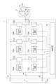
- FIG. 1 is a diagram showing the circuit configuration of a power conversion device according to one embodiment.
- the power conversion device 1 shown in FIG. 1 is an inverter device that converts DC power supplied from an external power source 2 into AC power capable of driving a motor 3.
- the power conversion device 1 is mounted on, for example, a vehicle.
- the external power source 2 is a DC power source, for example a storage battery.
- the power conversion device 1 has an input terminal 1a and an input terminal 1b.
- the input terminal 1a is connected to the positive terminal of the external power source 2, and the input terminal 1b is connected to the negative terminal of the external power source 2 and a reference potential V0.
- the motor 3 has three-phase coils 3u, 3v, and 3w.
- the coils 3u, 3v, and 3w are connected, for example, in a Y-connection.
- the motor 3 rotates when a current flows in a predetermined pattern through the coils 3u, 3v, and 3w.
- the connection of the coils 3u, 3v, and 3w is not limited to a Y-connection, and may be a delta connection.
- the power conversion device 1 includes switching circuit units 11uh, 11ul, 11vh, 11vl, 11wh, and 11wl (hereinafter referred to as “switching circuit units 11uh to 11wl”), driver circuits (circuit units) 13uh, 13ul, 13vh, 13vl, 13wh, and 13wl (hereinafter referred to as “driver circuits 13uh to 13wl”), a capacitor 14, and a control device 15.
- Each of the switching circuit units 11uh to 11wl incorporates a plurality of switching elements.
- the switching elements included in each of the switching circuit units 11uh to 11wl are exemplified by n-channel metal oxide semiconductor field effect transistors (MOSFETs).
- MOSFETs metal oxide semiconductor field effect transistors
- the switching elements are SiC MOSFETs.
- the switching elements may also be p-channel MOSFETs.
- the switching elements may also be insulated gate bipolar transistors (IGBTs) or GaN HEMTs.
- the switching circuit unit 11uh is the switching circuit unit of the upper arm of the U phase.
- the switching circuit unit 11ul is the switching circuit unit of the lower arm of the U phase.
- the switching circuit unit 11uh and the switching circuit unit 11ul are connected in series between the input terminal 1a and the input terminal 1b, and each has a first current terminal (drain terminal) T1 and a second current terminal (power source terminal) T2.
- the first current terminal T1 of the switching element included in the switching circuit unit 11uh is connected to the input terminal 1a.
- the second current terminal T2 of the switching element included in the switching circuit unit 11uh and the first current terminal T1 of the switching element included in the switching circuit unit 11ul are connected to each other and to the coil 3u.
- the second current terminal T2 of the switching element included in the switching circuit unit 11ul is connected to the input terminal 1b.
- the switching circuit unit 11vh is the switching circuit unit of the upper arm of the V phase.
- the switching circuit unit 11vl is the switching circuit unit of the lower arm of the V phase.
- the switching circuit unit 11vh and the switching circuit unit 11vl are connected in series between the input terminal 1a and the input terminal 1b, and each has a first current terminal (drain terminal) T1 and a second current terminal (power source terminal) T2.
- the first current terminal T1 of the switching element included in the switching circuit unit 11vh is connected to the input terminal 1a.
- the second current terminal T2 of the switching element included in the switching circuit unit 11vh and the first current terminal T1 of the switching element included in the switching circuit unit 11vl are connected to each other and to the coil 3v.
- the second current terminal T2 of the switching element included in the switching circuit unit 11vl is connected to the input terminal 1b.
- the switching circuit unit 11wh is the upper arm switching circuit unit of the W phase.
- the switching circuit unit 11wl is the lower arm switching circuit unit of the W phase.
- the switching circuit unit 11wh and the switching circuit unit 11wl are connected in series between the input terminal 1a and the input terminal 1b, and each has a first current terminal (drain terminal) T1 and a second current terminal (power source terminal) T2.
- the first current terminal T1 of the switching element included in the switching circuit unit 11wh is connected to the input terminal 1a.
- the second current terminal T2 of the switching element included in the switching circuit unit 11wh and the first current terminal T1 of the switching element included in the switching circuit unit 11wl are connected to each other and to the coil 3w.
- the second current terminal T2 of the switching element included in the switching circuit unit 11wl is connected to the input terminal 1b.
- a gate voltage (drive signal) Vg is applied from driver circuits 13uh to 13wl to the gates (control terminals) of the switching elements included in switching circuit units 11uh to 11wl.
- gate voltage Vg is applied to the gate
- a main current (source current) Is flows between the first current terminal T1 and the second current terminal T2 in each switching element.
- the switching element turns on, and a main current Is corresponding to the difference between the gate-source voltage and the threshold voltage flows between the first current terminal T1 and the second current terminal T2.
- Each of the driver circuits 13uh to 13wl is an active gate driver circuit that changes the gate voltage Vg based on the external command voltage Vref input from the control device 15 and the detection voltage, which is the voltage generated by the change in the main current Is. The details of the driver circuits will be described later.
- Capacitor 14 is charged by external power supply 2 and is used to suppress voltage fluctuations that occur when power conversion device 1 is operating. Capacitor 14 is connected in parallel with external power supply 2. Specifically, one end of capacitor 14 is connected to input terminal 1a, and the other end of capacitor 14 is connected to input terminal 1b. As capacitor 14, for example, a capacitor bank including multiple electrolytic capacitors is used.
- the control device 15 is a circuit that generates an external command voltage Vref for driving the switching circuit units 11uh to 11wl.
- the control device 15 determines a target current to flow through the motor 3 based on an external command (e.g., a required rotation speed), and derives an external command voltage Vref for flowing the target current.
- the control device 15 derives an external command voltage Vref for each of the switching circuit units 11uh to 11wl, and supplies the external command voltage Vref to each of the driver circuits 13uh to 13wl.
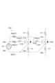
- FIG. 2 is a circuit diagram that shows a schematic diagram of the switching circuit section and driver circuit shown in FIG. 1.
- each of the driver circuits 13uh to 13wl has basically the same configuration
- each of the switching circuit sections 11uh to 11wl has basically the same configuration. Therefore, the driver circuit 13ul and the switching circuit section 11ul will be described in detail.
- the switching circuit unit 11ul includes two switching elements, switching element 11ula and switching element 11ulb.
- the switching element 11ula has a first wiring portion 21a into which the main current flows and a second wiring portion 22a from which the main current flows.
- a portion of one end of the first wiring portion 21a constitutes the first current terminal T1 of the switching element 11ula, and the other end is connected to the input terminal 1a via the switching circuit unit 11uh.
- a portion of one end of the second wiring portion 22a constitutes the second current terminal T2 of the switching element 11ula, and the other end is connected to the input terminal 1b.
- the first wiring portion 21a has an inductance component (floating inductance) Ld
- the second wiring portion 22a has an inductance component (floating inductance) Ls.
- the switching element 11ula also has a freewheeling diode Dula connected in parallel therewith. The cathode of the freewheel diode Dula is connected to the first current terminal T1 of the switching element 11ula, and the anode of the freewheel diode Dula is connected to the second current terminal T2 of the switching element 11ula.
- Switching element 11ulb is connected in parallel with switching element 11ula. Like switching element 11ula, switching element 11ulb has a first wiring portion 21b, a second wiring portion 22b, and a freewheeling diode Dulb. In this way, the switching circuit portion 11ul is formed by two switching elements 11ula and 11ulb connected in parallel, thereby reducing the conduction loss in the MOSFET.
- the driver circuit 13ul includes an adjustment circuit 27 having coils 23a, 23b, resistors 24a, 24b, and wiring 26, and a drive circuit 25.
- the drive circuit 25 generates a drive signal Vg for driving the switching elements 11ula, 11ulb based on an external command voltage Vref, and supplies the drive signal Vg to the gates of the switching elements 11ula, 11ulb.
- the adjustment circuit 27 is a circuit for adjusting the drive signal Vg supplied to the gates of the two switching elements 11ula, 11ulb to suppress imbalance in the main current (source current Is) flowing through each of the switching elements 11ula, 11ulb.
- the coil portion 23a is magnetically coupled to the inductance component Ld of the first wiring portion 21a and the inductance component Ls of the second wiring portion 22a, and generates a voltage at both ends of the coil portion 23a according to the change in the main current Is in the inductance component Ld and the change in the main current Is in the inductance component Ls.
- One end of the coil portion 23a is connected to the gate of the switching element 11ula, and the other end is connected via a resistor 24a to an output terminal 25a for outputting a drive signal Vg of the drive circuit 25.
- One end of the wiring portion 26 is connected to the source of the switching element 11ula, and the other end is connected to a reference potential terminal 25b for applying a reference potential of the drive circuit 25.
- the driver circuit 13ul has a configuration in which the coil portion 23a and the drive circuit 25 are connected in series between the gate and source of the switching element 11ula.
- the coil portion 23b is magnetically coupled to the inductance component Ld of the first wiring portion 21b and the inductance component Ls of the second wiring portion 22b.
- One end of the coil portion 23b is connected to the gate of the switching element 11ulb, and the other end is connected via a resistor 24b to an output terminal 25a for outputting a drive signal Vg of the drive circuit 25.
- One end of the wiring portion 26 is also connected to the source of the switching element 11ulb.
- the driver circuit 13ul has a configuration in which the coil portion 23b and the drive circuit 25 are connected in series between the gate and source of the switching element 11ulb.
- the driver circuit 13ul having the above configuration applies a drive signal Vg from which a large detection voltage has been subtracted to the gate of the switching element 11ula because the detection voltage becomes large when the source current Is in the inductance component Ld of the first wiring portion 21a and the inductance component Ls of the second wiring portion 22a is large.
- the driver circuit 13ul applies a drive signal Vg from which a small detection voltage has been subtracted, i.e., a gate voltage (drive signal Vg) with a relatively small subtraction, to the gate of the switching element 11ula because the detection voltage becomes small when the source current Is in the inductance component Ld of the first wiring portion 21a and the inductance component Ls of the second wiring portion 22a is small.
- the driver circuit 13ul adjusts the gate voltage applied to the gate of the switching element 11ula. Similarly, the driver circuit 13ul adjusts the gate voltage applied to the gate of the switching element 11ulb in response to fluctuations in the source current Is in the first wiring portion 21b and the second wiring portion 22b.
- the source current Is is reduced.
- the source current Is of one of the switching elements 11ula and 11ulb connected in parallel is reduced, the source current Is of the other increases accordingly. Therefore, with the above configuration, it is possible to suppress imbalance in the source current Is flowing through the switching elements 11ula and 11ulb.
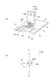
- Figure 3 is a plan view showing the positional relationship between the switching element 11ula and the coil portion 23a.
- Figure 4(a) is a perspective view showing an example of the implementation of the switching element 11ula and the coil portion 23a, and
- Figure 4(b) is a circuit diagram of the switching element 11ula shown in Figure 4(a).
- the positional relationship between the switching element 11ulb and the coil portion 23b is similar to that between the switching element 11ula and the coil portion 23a, so a description thereof will be omitted.
- the switching element 11ula has a first current terminal (drain terminal) T1, a second current terminal (power source terminal) T2, a driver source terminal T3, and a gate terminal T4, which are long conductive terminals extending in one direction from an end of the element package PKG.
- the first current terminal T1 is connected to the drain of the switching element body 28a in the element package PKG, and also constitutes the first wiring part 21a having an inductance component.
- the second current terminal T2 is connected to the source of the switching element body 28a in the element package PKG, and also constitutes the second wiring part 22a.
- the gate terminal T4 is connected to the gate of the switching element body 28a in the element package PKG.
- the driver source terminal T3 is connected to the source of the switching element body 28a in the element package PKG.
- a first current path 29 is formed through which the main current flows from the first wiring portion 21a to the first current terminal T1. That is, the first current path 29 includes both the wiring portion (inductance component) of the first current terminal T1 and the first wiring portion 21a in the element package PKG other than that wiring portion.
- a second current path 30 is formed through which the main current flows from the second current terminal T2 to the second wiring portion 22a. That is, the second current path 30 includes both the wiring portion (inductance component) of the second current terminal T2 and the second wiring portion 22a other than that wiring portion.
- the switching element 11ula is mounted on the circuit board 10 on which the driver circuits 13uh-13wl are mounted, with the element package PKG supported by the terminals T1-T4 so that it stands upright.
- the first current terminal T1 is connected to the wiring pattern P1 on the circuit board 10.
- the second current terminal T2 is connected to the wiring pattern P2 on the circuit board 10, and is connected to the input terminal 1b via the wiring pattern P2.
- the gate terminal T4 is connected to the wiring pattern P4 on the circuit board 10, and is connected to the coil portion 23a via the wiring pattern P4.
- the driver source terminal T3 is connected to the wiring pattern P3 on the circuit board 10, and is connected to the reference potential terminal 25b of the drive circuit 25 via the wiring pattern P3.
- the coil portion 23a is disposed between the first current path 29 on the first current terminal T1 and the second current path 30 on the second current terminal T2, and is configured to be magnetically coupled to both the first current path 29 and the second current path 30, and to be magnetically coupled to the inductance component Ld of the first current terminal T1 and the inductance component Ls of the second current terminal T2.
- "disposed between the first current path 29 on the first current terminal T1 and the second current path 30 on the second current terminal T2" has the following meaning.
- the coil portion 23a is disposed so as to overlap the gap between the first current terminal T1 and the second current terminal T2 when viewed from a direction perpendicular to the XY plane.
- the coil portion 23a is composed of a winding (conductor) 32a wound in a circular shape and an iron core 31a inserted inside the winding 32a.
- the winding 32a and the iron core 31a are fixed to both the first current terminal T1 and the second current terminal T2 using an insulating adhesive or an insulating member (e.g., a resin molded member).
- One end of the winding 32a is connected to the wiring pattern P5 on the circuit board 10 and is connected to the resistor 24a via the wiring pattern P5.
- the other end of the winding 32a is connected to the wiring pattern P6 on the circuit board 10 and is connected to the gate terminal T4 via the wiring pattern P6.
- the coil section 23a is arranged to be magnetically coupled to both the first current path 29 through which the main current flows into the switching element 11ula and the second current path 30 through which the main current flows out from the switching element 11ula, so that it is efficiently magnetically coupled to the inductance components Ld and Ls through which the main current flows.
- the inductance of the path through which the main current Is flows is increased, the surge voltage between the drain and source of the switching element will increase. Also, if the inductance of the coil section 23a is increased, the leakage inductance will increase and the operation of the driver circuit 13ul will slow down. In the power conversion device 1, it is possible to suppress the imbalance of the main current between multiple switching elements without causing a decrease in the surge voltage or a decrease in the operating speed of the driver circuit 13ul.
- the coil portion 23a is fixed to both the first current terminal T1 and the second current terminal T2.
- the first current path 29 and the second current path 30 through which the main current flows can be stably brought close to the coil portion 23a, and the distance between the first current path 29 and the second current path 30 and the coil portion 23a can be stabilized.
- the inductance components Ld and Ls through which the main current flows and the coil portion 23a are efficiently and stably magnetically coupled.
- the coil portion 23a is integrated with the first current terminal T1 and the second current terminal T2, it is not necessary to adjust the positional relationship between the coil portion 23a and the first current path 29 and the second current path 30, compared to the case in which the coil portion 23a is not fixed to the first current terminal T1 and the second current terminal T2, and the coil portion 23a can be easily provided at a position where it is magnetically coupled to the first current path 29 and the second current path 30. As a result, it is possible to further reduce switching loss.
- the coil portion 23a is a winding 32a, which is a conductor wound in a circular shape, and has an iron core 31a inserted inside the winding 32a.
- the iron core 31a reduces the magnetic resistance and increases the coupling coefficient, so that the inductance components Ld, Ls through which the main current flows are magnetically coupled even more strongly to the coil portion 23a.
- the stronger magnetic coupling makes it possible to increase the detection voltage generated in the coil portion 23a due to the change in the main current over time. As a result, it becomes possible to further reduce switching losses.
- the coil portion 23a is connected in series between the drive circuit 25 and the gate of the switching element 11ula to form the adjustment circuit 27. In this case, it is possible to reduce switching losses while maintaining the switching speed.
- each of the switching circuit units 11uh to 11wl includes two switching elements connected in parallel, but it may include three or more switching elements connected in parallel. In that case, a coil unit is provided corresponding to each switching element.
- the command conversion circuit 40 amplifies the external command voltage Vref input from the control device 15 to a drive signal Vg by a predetermined amplification factor and outputs the drive signal Vg to the adder circuit 42.
- the feedback conversion circuit 41 converts the voltage Vf generated across the coil portion 23a into a converted feedback voltage Vft by amplifying it by a predetermined amplification factor and outputs the converted feedback voltage Vft to the adder circuit 42.
- the adder circuit 42 adds the drive signal Vg and the converted feedback voltage Vft to generate a sum voltage Vad and applies the sum voltage Vad to the gate of the switching element 11ula.
- the coil portion 23a is fixed to both the first current terminal T1 and the second current terminal T2.
- the coil portion 23a may be fixed to the circuit board 10.
- a hole may be formed on the circuit board 10, and the tip of the coil portion 23a may be inserted into the hole, thereby fixing the coil portion 23a to the circuit board 10.
- the coil portion 23a may be fixed to the element package PKG, or may be fixed across the element package PKG and at least one of the first current terminal T1 and the second current terminal T2.
- the coil portion 23a may be fixed to at least one of the first current terminal T1 and the second current terminal T2.
- the coil portion 23a is disposed between the first current path 29 on the first current terminal T1 and the second current path 30 on the second current terminal T2.
- at least a portion of the coil portion 23a when viewed from a direction perpendicular to the XY plane, at least a portion of the coil portion 23a may be disposed so as to overlap the first wiring portion 21a or the second wiring portion 22a in the element package PKG.
- at least a portion of the coil portion 23a when viewed from a direction perpendicular to the XY plane, at least a portion of the coil portion 23a may be disposed so as to overlap the first current terminal T1 or the second current terminal T2.
Landscapes
- Engineering & Computer Science (AREA)
- Power Engineering (AREA)
- Power Conversion In General (AREA)
Applications Claiming Priority (2)
| Application Number | Priority Date | Filing Date | Title |
|---|---|---|---|
| JP2023-170068 | 2023-09-29 | ||
| JP2023170068A JP2025059772A (ja) | 2023-09-29 | 2023-09-29 | 電力変換装置 |
Publications (1)
| Publication Number | Publication Date |
|---|---|
| WO2025069614A1 true WO2025069614A1 (ja) | 2025-04-03 |
Family
ID=95202791
Family Applications (1)
| Application Number | Title | Priority Date | Filing Date |
|---|---|---|---|
| PCT/JP2024/023218 Pending WO2025069614A1 (ja) | 2023-09-29 | 2024-06-26 | 電力変換装置 |
Country Status (2)
| Country | Link |
|---|---|
| JP (1) | JP2025059772A (https=) |
| WO (1) | WO2025069614A1 (https=) |
Citations (3)
| Publication number | Priority date | Publication date | Assignee | Title |
|---|---|---|---|---|
| JP2017175602A (ja) * | 2016-01-29 | 2017-09-28 | トヨタ モーター エンジニアリング アンド マニュファクチャリング ノース アメリカ,インコーポレイティド | 電流/電力平衡化のための方法および装置 |
| JP2020005436A (ja) * | 2018-06-29 | 2020-01-09 | 株式会社デンソー | 電力用半導体装置及び電力変換装置 |
| JP2022061798A (ja) * | 2020-10-07 | 2022-04-19 | 株式会社豊田自動織機 | 電力変換装置 |
-
2023
- 2023-09-29 JP JP2023170068A patent/JP2025059772A/ja active Pending
-
2024
- 2024-06-26 WO PCT/JP2024/023218 patent/WO2025069614A1/ja active Pending
Patent Citations (3)
| Publication number | Priority date | Publication date | Assignee | Title |
|---|---|---|---|---|
| JP2017175602A (ja) * | 2016-01-29 | 2017-09-28 | トヨタ モーター エンジニアリング アンド マニュファクチャリング ノース アメリカ,インコーポレイティド | 電流/電力平衡化のための方法および装置 |
| JP2020005436A (ja) * | 2018-06-29 | 2020-01-09 | 株式会社デンソー | 電力用半導体装置及び電力変換装置 |
| JP2022061798A (ja) * | 2020-10-07 | 2022-04-19 | 株式会社豊田自動織機 | 電力変換装置 |
Also Published As
| Publication number | Publication date |
|---|---|
| JP2025059772A (ja) | 2025-04-10 |
Similar Documents
| Publication | Publication Date | Title |
|---|---|---|
| US5932995A (en) | Dual buck converter with coupled inductors | |
| CN102754327B (zh) | 电力变换装置 | |
| WO2015019519A1 (ja) | Dc-dcコンバータモジュール | |
| US11489437B2 (en) | DC inverter/converter current balancing for paralleled phase leg switches | |
| JP2014121123A (ja) | 電源装置 | |
| US20220311324A1 (en) | Control device for power conversion device | |
| WO2016149146A1 (en) | Paralleling of switching devices for high power circuits | |
| CN107710575A (zh) | 电力变换装置 | |
| KR102055461B1 (ko) | 전력 반도체 회로 | |
| CN104852615B (zh) | 电力变换装置以及缓冲电容器 | |
| JP6881399B2 (ja) | 電力用半導体装置及び電力変換装置 | |
| JP2014230138A (ja) | 半導体モジュールおよびスイッチング素子の駆動装置 | |
| JP5546892B2 (ja) | 昇圧回路 | |
| WO2025069614A1 (ja) | 電力変換装置 | |
| JP2017162884A (ja) | 半導体装置 | |
| JP2009273272A (ja) | インバータモジュール | |
| JP2008306867A (ja) | 電力変換装置および電気部品の接続方法 | |
| JP7555882B2 (ja) | パワー半導体モジュール及びそれを用いた電力変換装置 | |
| JP2024057802A (ja) | 電力変換装置 | |
| US12407254B2 (en) | Power supply semiconductor device and DC/DC converter | |
| JP7505450B2 (ja) | 電力変換装置 | |
| KR102735137B1 (ko) | 소형화된 가변 인덕터 | |
| JP5682194B2 (ja) | 電力変換装置 | |
| JP7413980B2 (ja) | 電力変換装置 | |
| JP7310263B2 (ja) | 電子部品 |
Legal Events
| Date | Code | Title | Description |
|---|---|---|---|
| 121 | Ep: the epo has been informed by wipo that ep was designated in this application |
Ref document number: 24871418 Country of ref document: EP Kind code of ref document: A1 |