WO2025069398A1 - 積層セラミックコンデンサ - Google Patents
積層セラミックコンデンサ Download PDFInfo
- Publication number
- WO2025069398A1 WO2025069398A1 PCT/JP2023/035697 JP2023035697W WO2025069398A1 WO 2025069398 A1 WO2025069398 A1 WO 2025069398A1 JP 2023035697 W JP2023035697 W JP 2023035697W WO 2025069398 A1 WO2025069398 A1 WO 2025069398A1
- Authority
- WO
- WIPO (PCT)
- Prior art keywords
- layer
- conductive resin
- laminate
- main surface
- resin layer
- Prior art date
- Legal status (The legal status is an assumption and is not a legal conclusion. Google has not performed a legal analysis and makes no representation as to the accuracy of the status listed.)
- Ceased
Links
Images




Classifications
-
- H—ELECTRICITY
- H01—ELECTRIC ELEMENTS
- H01G—CAPACITORS; CAPACITORS, RECTIFIERS, DETECTORS, SWITCHING DEVICES, LIGHT-SENSITIVE OR TEMPERATURE-SENSITIVE DEVICES OF THE ELECTROLYTIC TYPE
- H01G4/00—Fixed capacitors; Processes of their manufacture
- H01G4/30—Stacked capacitors
-
- H—ELECTRICITY
- H01—ELECTRIC ELEMENTS
- H01G—CAPACITORS; CAPACITORS, RECTIFIERS, DETECTORS, SWITCHING DEVICES, LIGHT-SENSITIVE OR TEMPERATURE-SENSITIVE DEVICES OF THE ELECTROLYTIC TYPE
- H01G4/00—Fixed capacitors; Processes of their manufacture
- H01G4/002—Details
- H01G4/005—Electrodes
- H01G4/012—Form of non-self-supporting electrodes
-
- H—ELECTRICITY
- H01—ELECTRIC ELEMENTS
- H01G—CAPACITORS; CAPACITORS, RECTIFIERS, DETECTORS, SWITCHING DEVICES, LIGHT-SENSITIVE OR TEMPERATURE-SENSITIVE DEVICES OF THE ELECTROLYTIC TYPE
- H01G4/00—Fixed capacitors; Processes of their manufacture
- H01G4/002—Details
- H01G4/228—Terminals
- H01G4/232—Terminals electrically connecting two or more layers of a stacked or rolled capacitor
-
- H—ELECTRICITY
- H01—ELECTRIC ELEMENTS
- H01G—CAPACITORS; CAPACITORS, RECTIFIERS, DETECTORS, SWITCHING DEVICES, LIGHT-SENSITIVE OR TEMPERATURE-SENSITIVE DEVICES OF THE ELECTROLYTIC TYPE
- H01G4/00—Fixed capacitors; Processes of their manufacture
- H01G4/002—Details
- H01G4/018—Dielectrics
- H01G4/06—Solid dielectrics
- H01G4/08—Inorganic dielectrics
- H01G4/12—Ceramic dielectrics
-
- H—ELECTRICITY
- H01—ELECTRIC ELEMENTS
- H01G—CAPACITORS; CAPACITORS, RECTIFIERS, DETECTORS, SWITCHING DEVICES, LIGHT-SENSITIVE OR TEMPERATURE-SENSITIVE DEVICES OF THE ELECTROLYTIC TYPE
- H01G4/00—Fixed capacitors; Processes of their manufacture
- H01G4/002—Details
- H01G4/228—Terminals
- H01G4/232—Terminals electrically connecting two or more layers of a stacked or rolled capacitor
- H01G4/2325—Terminals electrically connecting two or more layers of a stacked or rolled capacitor characterised by the material of the terminals
Definitions
- the present invention relates to a multilayer ceramic capacitor.
- Patent Document 1 is an example of this type of technology.
- Patent Document 1 describes a multilayer ceramic capacitor that has external electrodes with a layered configuration in which an electrode layer formed by applying a conductive paste by dipping and baking the paste, a conductive epoxy-based thermosetting resin layer, a nickel-plated layer, and a tin-based layer are sequentially laminated.
- the objective of the present invention is to provide a multilayer ceramic capacitor that can improve resistance to bending.
- the multilayer ceramic capacitor according to the present invention includes a laminate including a plurality of laminated dielectric layers, the laminate having a first main surface and a second main surface that face each other in a height direction, a first side surface and a second side surface that face each other in a width direction perpendicular to the height direction, and a first end surface and a second end surface that face each other in a length direction perpendicular to the height direction and the width direction, a first internal electrode layer that is disposed on the plurality of dielectric layers and exposed to the first end surface, a second internal electrode layer that is disposed on the plurality of dielectric layers and exposed to the second end surface, a first external electrode that is disposed on the first end surface, and a second external electrode that is disposed on the second end surface, in which the first external electrode and the second external electrode have a base electrode layer that includes a metal component, a conductive resin layer that is disposed on the base electrode layer and includes a filler powder and a resin component, and a plating layer
- the present invention provides a multilayer ceramic capacitor that can improve resistance to bending.
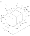
- FIG. 1 is an external perspective view of a multilayer ceramic capacitor according to an embodiment of the present invention
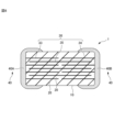
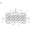
- 2 is a cross-sectional view taken along line II-II of the multilayer ceramic capacitor shown in FIG. 3 is a cross-sectional view taken along line III-III of the multilayer ceramic capacitor shown in FIG. 2.
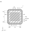
- 4 is a cross-sectional view taken along line IV-IV of the multilayer ceramic capacitor shown in FIG. 2.
- 3 is an enlarged view of a V portion of the multilayer ceramic capacitor shown in FIG. 2, and is a schematic diagram for explaining in detail the structure of a ridge line portion of the multilayer ceramic capacitor.
- FIG. FIG. 2 is a schematic diagram showing an example of a configuration of a double-structure multilayer ceramic capacitor.
- FIG. 2 is a schematic diagram showing an example of a configuration of a triple-structure multilayer ceramic capacitor.
- FIG. 2 is a schematic diagram showing an example of a configuration of a four-row multilayer ceramic capacitor.
- FIG. 1 is an external perspective view of the multilayer ceramic capacitor 1 of this embodiment.
- Fig. 2 is a cross-sectional view taken along line II-II of the multilayer ceramic capacitor 1 in Fig. 1.
- Fig. 3 is a cross-sectional view taken along line III-III of the multilayer ceramic capacitor 1 in Fig. 2.
- Fig. 4 is a cross-sectional view taken along line IV-IV of the multilayer ceramic capacitor 1 in Fig. 2.
- the multilayer ceramic capacitor 1 has a laminate 10 and an external electrode 40.
- FIGS. 1 to 4 show an XYZ orthogonal coordinate system.
- the length direction L of the multilayer ceramic capacitor 1 and the laminate 10 corresponds to the X direction.
- the width direction W of the multilayer ceramic capacitor 1 and the laminate 10 corresponds to the Y direction.
- the stacking direction T as the height direction of the multilayer ceramic capacitor 1 and the laminate 10 corresponds to the Z direction.
- the cross section shown in FIG. 2 is also called the LT cross section.
- the cross section shown in FIG. 3 is also called the WT cross section.
- the cross section shown in FIG. 4 is also called the LW cross section.
- the laminate 10 includes a first main surface TS1 and a second main surface TS2 that face the stacking direction T, a first side surface WS1 and a second side surface WS2 that face the width direction W that is perpendicular to the stacking direction T, and a first end surface LS1 and a second end surface LS2 that face the length direction L that is perpendicular to the stacking direction T and the width direction W.
- the laminate 10 has a generally rectangular parallelepiped shape.
- the dimension of the laminate 10 in the length direction L is not necessarily longer than the dimension in the width direction W. It is preferable that the corners and ridges of the laminate 10 are rounded. A corner is a portion where three faces of the laminate intersect, and a ridge is a portion where two faces of the laminate intersect. Incidentally, unevenness may be formed on part or all of the surfaces constituting the laminate 10.
- the dimensions of the laminate 10 are not particularly limited, but if the dimension of the laminate 10 in the length direction L is the L dimension, it is preferable that the L dimension is 0.2 mm or more and 10 mm or less. If the dimension of the laminate 10 in the stacking direction T is the T dimension, it is preferable that the T dimension is 0.1 mm or more and 10 mm or less. If the dimension of the laminate 10 in the width direction W is the W dimension, it is preferable that the W dimension is 0.1 mm or more and 10 mm or less.
- the laminate 10 has an inner layer portion 11, and a first main surface side outer layer portion 12A as a first outer layer portion and a second main surface side outer layer portion 12B as a second outer layer portion arranged to sandwich the inner layer portion 11 in the stacking direction T.
- the inner layer portion 11 includes a plurality of dielectric layers 20 as a plurality of ceramic layers, and a plurality of internal electrode layers 30 as a plurality of internal conductor layers.
- the inner layer portion 11 includes the internal electrode layer 30 located closest to the first principal surface TS1 in the stacking direction T to the internal electrode layer 30 located closest to the second principal surface TS2.
- the multiple internal electrode layers 30 are arranged opposite each other with the dielectric layer 20 interposed therebetween.
- the inner layer portion 11 is a portion that generates electrostatic capacitance and essentially functions as a capacitor.
- the plurality of dielectric layers 20 are made of a dielectric material.
- the dielectric material may be, for example, a dielectric ceramic containing components such as BaTiO3 , CaTiO3 , SrTiO3 , or CaZrO3 .
- the dielectric material may also be a material in which a subcomponent such as a Mn compound, an Fe compound, a Cr compound, a Co compound, or a Ni compound is added to the main components.
- the thickness of the dielectric layer 20 is preferably 0.5 ⁇ m or more and 30 ⁇ m or less.
- the number of dielectric layers 20 to be stacked is preferably 10 or more and 1500 or less.
- the number of dielectric layers 20 is the total number of the dielectric layers in the inner layer portion 11 and the dielectric layers in the first main surface side outer layer portion 12A and the second main surface side outer layer portion 12B.
- the multiple internal electrode layers 30 have first internal electrode layers 31 as multiple first internal conductor layers and second internal electrode layers 32 as multiple second internal conductor layers.
- the multiple first internal electrode layers 31 are arranged on the multiple dielectric layers 20.
- the multiple second internal electrode layers 32 are arranged on the multiple dielectric layers 20.
- the multiple first internal electrode layers 31 and the multiple second internal electrode layers 32 are arranged alternately in the stacking direction T of the laminate 10 with the dielectric layers 20 interposed between them.
- the first internal electrode layers 31 and the second internal electrode layers 32 are arranged so as to sandwich the dielectric layers 20 between them.
- the first internal electrode layer 31 has a first opposing portion 31A that faces the second internal electrode layer 32, and a first lead-out portion 31B that is led out from the first opposing portion 31A to the first end surface LS1.
- the first lead-out portion 31B is exposed to the first end surface LS1.
- the second internal electrode layer 32 has a second opposing portion 32A that faces the first internal electrode layer 31, and a second lead-out portion 32B that is led out from the second opposing portion 32A to the second end surface LS2.
- the second lead-out portion 32B is exposed to the second end surface LS2.
- the first opposing portion 31A and the second opposing portion 32A face each other via the dielectric layer 20, forming a capacitance and exhibiting the characteristics of a capacitor.
- the shapes of the first opposing portion 31A and the second opposing portion 32A are not particularly limited, but are preferably rectangular. However, the corners of the rectangular shape may be rounded or the corners of the rectangular shape may be formed at an angle.
- the shapes of the first pull-out portion 31B and the second pull-out portion 32B are not particularly limited, but are preferably rectangular. However, the corners of the rectangular shape may be rounded or the corners of the rectangular shape may be formed at an angle.
- the dimension in the width direction W of the first opposing portion 31A and the dimension in the width direction W of the first pull-out portion 31B may be the same, or one of the dimensions may be smaller.
- the dimension in the width direction W of the second opposing portion 32A and the dimension in the width direction W of the second pull-out portion 32B may be the same, or one of the dimensions may be smaller.
- the first internal electrode layer 31 and the second internal electrode layer 32 are made of an appropriate conductive material, such as a metal such as Ni, Cu, Ag, Pd, or Au, or an alloy containing at least one of these metals. When an alloy is used, the first internal electrode layer 31 and the second internal electrode layer 32 may be made of, for example, an Ag-Pd alloy.
- each of the first internal electrode layer 31 and the second internal electrode layer 32 is preferably, for example, about 0.2 ⁇ m or more and 2.0 ⁇ m or less.
- the total number of the first internal electrode layers 31 and the second internal electrode layers 32 is preferably 10 or more and 1500 or less.
- the first main surface side outer layer portion 12A is located on the first main surface TS1 side of the laminate 10.
- the first main surface side outer layer portion 12A is an assembly of multiple dielectric layers 20 located between the first main surface TS1 and the internal electrode layer 30 closest to the first main surface TS1.
- the dielectric layer 20 used in the first main surface side outer layer portion 12A may be the same as the dielectric layer 20 used in the internal layer portion 11, or may be a dielectric layer made of a different material.
- the second main surface side outer layer portion 12B is located on the second main surface TS2 side of the laminate 10.
- the second main surface side outer layer portion 12B is an assembly of multiple dielectric layers 20 located between the second main surface TS2 and the internal electrode layer 30 closest to the second main surface TS2.
- the dielectric layer 20 used in the second main surface side outer layer portion 12B may be the same as the dielectric layer 20 used in the internal layer portion 11, or may be a dielectric layer made of a different material.
- the laminate 10 has an opposing electrode portion 11E.
- the opposing electrode portion 11E is a portion where the first opposing portion 31A of the first internal electrode layer 31 and the second opposing portion 32A of the second internal electrode layer 32 face each other.
- the opposing electrode portion 11E is configured as a part of the inner layer portion 11.
- Figure 4 shows the range of the width direction W and length direction L of the opposing electrode portion 11E.
- the opposing electrode portion 11E is also called the effective portion of the capacitor.
- the laminate 10 has a side surface outer layer portion.
- the side surface outer layer portion has a first side surface outer layer portion WG1 and a second side surface outer layer portion WG2.
- the first side surface outer layer portion WG1 is a portion including the dielectric layer 20 located between the opposing electrode portion 11E and the first side surface WS1.
- the second side surface outer layer portion WG2 is a portion including the dielectric layer 20 located between the opposing electrode portion 11E and the second side surface WS2.
- Figures 3 and 4 show the range of the width direction W of the first side surface outer layer portion WG1 and the second side surface outer layer portion WG2.
- the side surface outer layer portion is also called a W gap or a side gap.
- the laminate 10 has an end surface side outer layer portion.
- the end surface side outer layer portion has a first end surface side outer layer portion LG1 and a second end surface side outer layer portion LG2.
- the first end surface side outer layer portion LG1 is a portion including a dielectric layer 20 located between the counter electrode portion 11E and the first end surface LS1.
- the second end surface side outer layer portion LG2 is a portion including a dielectric layer 20 located between the counter electrode portion 11E and the second end surface LS2.
- Figures 2 and 4 show the range of the length direction L of the first end surface side outer layer portion LG1 and the second end surface side outer layer portion LG2.
- the end surface side outer layer portion is also called an L gap or an end gap.
- the external electrode 40 has a first external electrode 40A arranged on the first end face LS1 side and a second external electrode 40B arranged on the second end face LS2 side.
- the first external electrode 40A is disposed on the first end face LS1.
- the first external electrode 40A is connected to the first internal electrode layer 31.
- the first external electrode 40A is disposed on a portion of the first main surface TS1 and a portion of the second main surface TS2.
- the first external electrode 40A is formed extending from the first end face LS1 to a portion of the first main surface TS1 and a portion of the second main surface TS2, as well as a portion of the first side surface WS1 and a portion of the second side surface WS2.
- the second external electrode 40B is disposed on the second end face LS2.
- the second external electrode 40B is connected to the second internal electrode layer 32.
- the second external electrode 40B is disposed on a portion of the first main surface TS1 and a portion of the second main surface TS2.
- the second external electrode 40B is formed extending from the second end face LS2 to a portion of the first main surface TS1 and a portion of the second main surface TS2, as well as a portion of the first side surface WS1 and a portion of the second side surface WS2.
- the first opposing portion 31A of the first internal electrode layer 31 and the second opposing portion 32A of the second internal electrode layer 32 face each other via the dielectric layer 20, forming a capacitance. Therefore, the characteristics of a capacitor are expressed between the first external electrode 40A to which the first internal electrode layer 31 is connected and the second external electrode 40B to which the second internal electrode layer 32 is connected.
- the first external electrode 40A has a first base electrode layer 50A containing a metal component, a first conductive resin layer 60A disposed on the first base electrode layer 50A, and a first plating layer 70A disposed on the first conductive resin layer 60A.
- the first plating layer 70A has a first Ni plating layer 71A as a lower plating layer and a first Sn plating layer 72A as an upper plating layer.
- the second external electrode 40B has a second base electrode layer 50B containing a metal component, a second conductive resin layer 60B disposed on the second base electrode layer 50B, and a second plating layer 70B disposed on the second conductive resin layer 60B.
- the second plating layer 70B has a second Ni plating layer 71B as a lower plating layer and a second Sn plating layer 72B as an upper plating layer.
- the basic configuration of each layer constituting the first external electrode 40A and the second external electrode 40B is the same. Furthermore, the first external electrode 40A and the second external electrode 40B are generally plane-symmetrical with respect to the LW cross section at the center of the longitudinal direction L of the multilayer ceramic capacitor 1. Therefore, when there is no need to particularly distinguish between the first external electrode 40A and the second external electrode 40B, the first external electrode 40A and the second external electrode 40B may be collectively referred to as the external electrode 40. Furthermore, when there is no need to particularly distinguish between the first base electrode layer 50A and the second base electrode layer 50B, the first base electrode layer 50A and the second base electrode layer 50B may be collectively referred to as the base electrode layer 50.
- the first conductive resin layer 60A and the second conductive resin layer 60B may be collectively referred to as the conductive resin layer 60.
- the first plating layer 70A and the second plating layer 70B may be collectively referred to as the plating layer 70.
- the first Ni plating layer 71A and the second Ni plating layer 71B may be collectively referred to as the Ni plating layer 71.
- the first Sn plating layer 72A and the second Sn plating layer 72B may be collectively referred to as the Sn plating layer 72.
- the first main surface TS1 and the second main surface TS2 may be collectively referred to as the main surface TS.
- the first side surface WS1 and the second side surface WS2 may be collectively referred to as the side surface WS.
- the first end surface LS1 and the second end surface LS2 may be collectively referred to as the end surface LS.
- the base electrode layer 50 has a first base electrode layer 50A and a second base electrode layer 50B.
- the first base electrode layer 50A is disposed on the first end face LS1.
- the first base electrode layer 50A is connected to the first internal electrode layer 31.
- the first base electrode layer 50A is formed extending from the first end face LS1 to a portion of the first main surface TS1 and a portion of the second main surface TS2, as well as a portion of the first side surface WS1 and a portion of the second side surface WS2.
- the second base electrode layer 50B is disposed on the second end face LS2.
- the second base electrode layer 50B is connected to the second internal electrode layer 32.
- the second base electrode layer 50B is formed to extend from the second end face LS2 to a portion of the first main surface TS1 and a portion of the second main surface TS2, as well as a portion of the first side surface WS1 and a portion of the second side surface WS2.
- the first base electrode layer 50A and the second base electrode layer 50B of this embodiment are baked layers.
- the baked layer preferably contains a metal component and either a glass component or a ceramic component, or both. This can improve the adhesion between the laminate 10 and the base electrode layer.
- the metal component contains at least one selected from, for example, Cu, Ni, Ag, Pd, an Ag-Pd alloy, Au, etc.
- the glass component contains at least one selected from, for example, B, Si, Ba, Mg, Al, Li, etc. When the glass component is present, it can help sinter the metal component in the base electrode layer and promote sintering.
- the ceramic component may be the same type of ceramic material as the dielectric layer 20, or a different type of ceramic material.
- the ceramic component includes at least one selected from, for example, BaTiO 3 , CaTiO 3 , (Ba,Ca)TiO 3 , SrTiO 3 , CaZrO 3 , and the like.
- the baked layer is, for example, a conductive paste containing glass and metal applied to the laminate and baked.
- the baked layer may be formed by simultaneously baking a laminated chip having an internal electrode and a dielectric layer and a conductive paste applied to the laminated chip, or by baking a laminated chip having an internal electrode and a dielectric layer to obtain a laminate, and then applying a conductive paste to the laminate and baking it.
- a laminated chip having an internal electrode and a dielectric layer and a conductive paste applied to the laminated chip are simultaneously baked, it is preferable to form the baked layer by adding a ceramic material instead of a glass component and baking it. In this case, it is particularly preferable to use the same type of ceramic material as the dielectric layer 20 as the added ceramic material.
- the baked layer may be a multi-layered layer.
- the thickness in the longitudinal direction of the first base electrode layer 50A located on the first end surface LS1 is preferably, for example, about 2 ⁇ m or more and 220 ⁇ m or less at the center of the stacking direction T and width direction W of the first base electrode layer 50A.
- the thickness in the longitudinal direction of the second base electrode layer 50B located on the second end surface LS2 is preferably, for example, about 2 ⁇ m or more and 220 ⁇ m or less at the center of the stacking direction T and width direction W of the second base electrode layer 50B.
- the thickness in the stacking direction of the first base electrode layer 50A provided on this portion is preferably, for example, about 4 ⁇ m or more and 40 ⁇ m or less at the center in the length direction L and width direction W of the first base electrode layer 50A provided on this portion.
- the widthwise thickness of the first base electrode layer 50A provided on this portion is preferably, for example, about 4 ⁇ m or more and 40 ⁇ m or less at the center of the length direction L and stacking direction T of the first base electrode layer 50A provided on this portion.
- the thickness in the stacking direction of the second base electrode layer 50B provided on this portion is preferably, for example, about 4 ⁇ m or more and 40 ⁇ m or less at the center in the length direction L and width direction W of the second base electrode layer 50B provided on this portion.
- the widthwise thickness of the second base electrode layer 50B provided on this portion is preferably, for example, about 4 ⁇ m or more and 40 ⁇ m or less at the center of the length direction L and stacking direction T of the second base electrode layer 50B provided on this portion.
- the external electrode 40 has a conductive resin layer 60 that contains a resin component and a metal component and is disposed on the base electrode layer 50.
- the conductive resin layer 60 has a first conductive resin layer 60A and a second conductive resin layer 60B.
- the first conductive resin layer 60A is arranged to cover the first underlying electrode layer 50A.
- the first conductive resin layer 60A is formed to extend from the first end face LS1 to a portion of the first main surface TS1 and a portion of the second main surface TS2, as well as a portion of the first side surface WS1 and a portion of the second side surface WS2.
- the second conductive resin layer 60B is arranged to cover the second underlying electrode layer 50B.
- the second conductive resin layer 60B is formed to extend from the second end face LS2 to a portion of the first main surface TS1 and a portion of the second main surface TS2, as well as a portion of the first side surface WS1 and a portion of the second side surface WS2.
- the dimension in the length direction L on the first main surface TS1 and the second main surface TS2 of the first conductive resin layer 60A is longer than the dimension in the length direction L on the first main surface TS1 and the second main surface TS2 of the first base electrode layer 50A.
- the dimension in the length direction L on the first main surface TS1 and the second main surface TS2 of the second conductive resin layer 60B is longer than the dimension in the length direction L on the first main surface TS1 and the second main surface TS2 of the second base electrode layer 50B.
- the thickness in the longitudinal direction of the first conductive resin layer 60A located on the first end surface LS1 side is preferably, for example, about 5 ⁇ m or more and 200 ⁇ m or less at the center of the stacking direction T and width direction W of the first conductive resin layer 60A.
- the thickness in the longitudinal direction of the second conductive resin layer 60B located on the second end surface LS2 side is preferably, for example, about 5 ⁇ m or more and 200 ⁇ m or less at the center of the stacking direction T and width direction W of the second conductive resin layer 60B.
- the thickness in the stacking direction of the first conductive resin layer 60A provided on this portion is preferably, for example, about 5 ⁇ m or more and 200 ⁇ m or less at the center in the length direction L and width direction W of the first conductive resin layer 60A provided on this portion.
- the widthwise thickness of the first conductive resin layer 60A provided on this portion is preferably, for example, about 5 ⁇ m or more and 200 ⁇ m or less at the center in the length direction L and stacking direction T of the first conductive resin layer 60A provided on this portion.
- the thickness in the stacking direction of the second conductive resin layer 60B provided on this portion is preferably, for example, about 5 ⁇ m or more and 200 ⁇ m or less at the center in the length direction L and width direction W of the second conductive resin layer 60B provided on this portion.
- the widthwise thickness of the second conductive resin layer 60B provided on this portion is preferably, for example, about 5 ⁇ m or more and 200 ⁇ m or less at the center in the length direction L and stacking direction T of the second conductive resin layer 60B provided on this portion.
- the conductive resin layer 60 is disposed on the base electrode layer 50.
- a plating layer 70 is disposed so as to cover the conductive resin layer 60.
- the plating layer 70 has a Ni plating layer 71 and a Sn plating layer 72.
- the conductive resin layer 60 has a resin portion as a resin component and conductive filler as filler powder dispersed within the resin portion.
- the resin portion of the conductive resin layer 60 may contain at least one selected from various known thermosetting resins, such as epoxy resin, phenoxy resin, phenol resin, urethane resin, silicone resin, polyimide resin, etc. Among them, epoxy resin, which has excellent heat resistance, moisture resistance, adhesion, etc., is one of the most suitable resins. In addition, it is preferable that the resin portion of the conductive resin layer 60 contains a hardener together with the thermosetting resin. When an epoxy resin is used as the base resin, the hardener of the epoxy resin may be various known compounds such as phenol-based, amine-based, acid anhydride-based, imidazole-based, active ester-based, and amide-imide-based compounds.
- the conductive resin layer 60 contains such a resin portion, it is more flexible than, for example, the base electrode layer 50, which is made of a plating film or a fired product of metal components and glass components. Therefore, even if the multilayer ceramic capacitor 1 is subjected to a physical impact or an impact due to a thermal cycle, the conductive resin layer 60 functions as a buffer layer. Therefore, the conductive resin layer 60 suppresses the occurrence of cracks in the multilayer ceramic capacitor 1.
- the conductive fillers are dispersed in a substantially uniform distribution within the resin portion.
- the conductive fillers are mainly responsible for the electrical conductivity of the conductive resin layer 60. Specifically, when multiple conductive fillers come into contact with each other, an electrical path is formed within the conductive resin layer 60, providing electrical conductivity between the base electrode layer 50 and the plating layer 70.
- the metal that constitutes the conductive filler may be Ag alone, an alloy containing Ag, or a metal powder with Ag coating on the surface.
- Ag has the lowest resistivity of all metals, making it suitable as an electrode material. Also, since Ag is a precious metal, it is resistant to oxidation and has high weather resistance. Therefore, Ag metal powder is suitable as a conductive filler. Also, when using metal powder with Ag coating on the surface, it is preferable to use Cu, Ni, Sn, Bi, or an alloy powder containing these metal powders.
- the conductive filler may be Cu or Ni that has been subjected to an anti-oxidation treatment.
- the conductive filler may also be a metal powder in which the surface of the metal powder is coated with Sn, Ni, or Cu.
- the metal powder is preferably Ag, Cu, Ni, Sn, Bi, or an alloy powder thereof.
- the conductive filler has a Cu particle as a core. It is also more preferable that at least a part of the surface of the Cu particle is coated with a Cu-Ag alloy of Cu and Ag. At least a part of the surface of the Cu particle may be coated with Ag. This improves the affinity with Ni plating and improves the electrical properties.
- the shape of the conductive filler is not particularly limited.
- the conductive filler may be spherical, flat, or the like. It is preferable to use a mixture of spherical metal powder and flat metal powder.
- the conductive filler as the filler powder includes flat powder or spherical powder.
- the average particle diameter of the conductive filler may be, for example, 0.3 ⁇ m or more and 10 ⁇ m or less.
- the average particle size of the conductive filler contained in the conductive resin layer 60 is measured by calculating it using a laser diffraction particle size measurement method based on ISO 13320, regardless of the shape of the conductive filler.
- the plating layer 70 has a first plating layer 70A and a second plating layer 70B.
- the first plating layer 70A is disposed so as to cover the first conductive resin layer 60A.
- the first plating layer 70A is disposed so as to extend from the first end surface LS1 to a portion of the first main surface TS1 and a portion of the second main surface TS2, as well as a portion of the first side surface WS1 and a portion of the second side surface WS2.
- the second plating layer 70B is disposed so as to cover the second conductive resin layer 60B.
- the second plating layer 70B is disposed so as to extend from the first end surface LS1 to a portion of the first main surface TS1 and a portion of the second main surface TS2, as well as a portion of the first side surface WS1 and a portion of the second side surface WS2.
- the plating layer 70 preferably has a two-layer structure of a Ni plating layer 71 and a Sn plating layer 72.
- a first Sn plating layer 72A is preferably disposed on the first Ni plating layer 71A
- a second Sn plating layer 72B is preferably disposed on the second Ni plating layer 71B.
- the Ni plating layer 71 prevents the base electrode layer 50 and the conductive resin layer 60 from being eroded by the solder when mounting the multilayer ceramic capacitor 1.
- the Sn plating layer 72 improves the wettability of the solder when mounting the multilayer ceramic capacitor 1. This makes it easier to mount the multilayer ceramic capacitor 1.
- each of the first Ni plating layer 71A and the first Sn plating layer 72A is preferably 5 ⁇ m or more and 15 ⁇ m or less.
- each of the second Ni plating layer 71B and the second Sn plating layer 72B is preferably 5 ⁇ m or more and 15 ⁇ m or less.
- FIG. 5 is an enlarged view of the V portion of the multilayer ceramic capacitor 1 shown in FIG. 2, and is a schematic diagram for explaining in detail the structure of the ridge portion 10a of the multilayer ceramic capacitor 1, which will be described later.
- the four ridge portions 10a1 to 10a4 of the laminate 10 shown in FIG. 2 have the same basic configuration, and the four extension portions E1 to E4 of the external electrode 40 also have the same basic configuration. Therefore, the four regions will be explained using FIG. 5 as a representative diagram.
- the first external electrode 40A and the second external electrode 40B have the same basic configuration, so in FIG. 5 they are also collectively shown as the external electrode 40. The same applies to the other layers that make up the first external electrode 40A and the second external electrode 40B.
- the external electrode 40 has a base electrode layer 50, a conductive resin layer 60 disposed on the base electrode layer 50, and a plating layer 70 disposed on the conductive resin layer 60.
- the external electrode 40 has an extension portion E disposed to extend to a part of the main surface TS.
- the laminate 10 has a ridge portion 10a at the intersection of the end surface LS and the main surface TS.
- a conductive resin layer 60 is disposed on the ridge portion 10a of the laminate 10.
- the first external electrode 40A and the second external electrode 40B each have an extension E that is arranged to extend to a portion of the first main surface TS1 and a portion of the second main surface TS2.
- the first external electrode 40A and the second external electrode 40B each further have an extension E that is arranged to extend to a portion of the first side surface WS1 and a portion of the second side surface WS2.
- the extension portion E in this embodiment has a first extension portion E1, a second extension portion E2, a third extension portion E3, a fourth extension portion E4, a fifth extension portion E5, a sixth extension portion E6, a seventh extension portion E7, and an eighth extension portion E8, as shown in Figures 2, 4, and 5.
- the first extension portion E1 is a portion of the first external electrode 40A that is arranged to extend over a portion of the first main surface TS1 as shown in Figures 2 and 5.
- the second extension portion E2 is a portion of the first external electrode 40A that is arranged to extend over a portion of the second main surface TS2 as shown in Figures 2 and 5.
- the third extension portion E3 is a portion of the second external electrode 40B that is arranged to extend over a portion of the first main surface TS1 as shown in Figures 2 and 5.
- the fourth extension portion E4 is a portion of the second external electrode 40B that is arranged to extend over a portion of the second main surface TS2 as shown in Figures 2 and 5.
- the fifth extension E5 is a portion of the first external electrode 40A that is arranged to extend onto a portion of the first side surface WS1 as shown in FIG. 4.
- the sixth extension E6 is a portion of the first external electrode 40A that is arranged to extend onto a portion of the second side surface WS2 as shown in FIG. 4.
- the seventh extension E7 is a portion of the second external electrode 40B that is arranged to extend over a portion of the first side surface WS1 as shown in FIG. 4.
- the eighth extension E8 is a portion of the second external electrode 40B that is arranged to extend over a portion of the second side surface WS2 as shown in FIG. 4.
- the configuration of the extension portion E is not limited to this.
- the extension portion E may be disposed on at least the first main surface TS1 and the second main surface TS2 of the first external electrode 40A and the second external electrode 40B.
- the laminate 10 has ridges 10a at the intersection of the first end face LS1 and the first main surface TS1, the intersection of the first end face LS1 and the second main surface TS2, the intersection of the second end face LS2 and the first main surface TS1, and the intersection of the second end face LS2 and the second main surface TS2.
- the laminate 10 also has ridges 10a at the intersection of the first end face LS1 and the first side surface WS1, the intersection of the first end face LS1 and the second side surface WS2, the intersection of the second end face LS2 and the first side surface WS1, and the intersection of the second end face LS2 and the second side surface WS2.
- the ridge portion 10a has a first ridge portion 10a1, a second ridge portion 10a2, a third ridge portion 10a3, a fourth ridge portion 10a4, a fifth ridge portion 10a5, a sixth ridge portion 10a6, a seventh ridge portion 10a7, and an eighth ridge portion 10a8.
- the first ridge portion 10a1 is the intersection of the first end surface LS1 and the first main surface TS1 as shown in Figures 2 and 5.
- the second ridge portion 10a2 is the intersection of the first end surface LS1 and the second main surface TS2 as shown in Figures 2 and 5.
- the third ridge portion 10a3 is the intersection of the second end surface LS2 and the first main surface TS1 as shown in Figures 2 and 5.
- the fourth ridge portion 10a4 is the intersection of the second end surface LS2 and the second main surface TS2 as shown in Figures 2 and 5.
- the fifth ridge portion 10a5 is the intersection of the first end face LS1 and the first side face WS1 as shown in FIG. 4.
- the sixth ridge portion 10a6 is the intersection of the first end face LS1 and the second side face WS2 as shown in FIG. 4.
- the seventh ridge portion 10a7 is the intersection of the second end face LS2 and the first side face WS1 as shown in FIG. 4.
- the eighth ridge portion 10a8 is the intersection of the second end face LS2 and the second side face WS2 as shown in FIG. 4.
- a conductive resin layer 60 is disposed on the ridgeline portion 10a of the laminate 10 via the base electrode layer 50. That is, the conductive resin layer 60 is disposed on the ridgeline portion 10a of the laminate 10 so as to be sandwiched between the base electrode layer 50 and the plating layer 70.
- the thickness of the conductive resin layer 60 on the ridgeline portion 10a of the laminate 10 is thinner than the thickness of the conductive resin layer 60 in other parts, i.e., the thickness of the conductive resin layer 60 on the end surface LS of the laminate 10, the main surface TS of the laminate 10, and the side surface WS of the laminate.
- the film thickness t of the conductive resin layer 60 on the ridgeline portion 10a is preferably 0.8 ⁇ m or more and 8 ⁇ m or less.
- the plating layer 70 When the plating layer 70 is disposed across the ridge portion 10a, deflection occurring on the main surface TS or side surface WS of the external electrode 40 may propagate to the end surface LS of the laminate 10.
- the conductive resin layer 60 when the conductive resin layer 60 is disposed on the ridge portion 10a, the flexibility of the conductive resin layer 60 can prevent deflection occurring on the main surface TS or side surface WS of the external electrode 40 from propagating to the end surface LS of the laminate 10.
- a first conductive resin layer 60A is disposed on the first ridge portion 10a1 of the laminate 10 according to this embodiment, as shown in Figures 2 and 5.
- a first conductive resin layer 60A is disposed on the second ridge portion 10a2 of the laminate 10 according to this embodiment, as shown in Figures 2 and 5.
- a second conductive resin layer 60B is disposed on the third ridge portion 10a3 of the laminate 10 according to this embodiment, as shown in Figures 2 and 5.
- a second conductive resin layer 60B is disposed on the fourth ridge portion 10a4 of the laminate 10 according to this embodiment, as shown in Figures 2 and 5.
- a first conductive resin layer 60A is disposed on the fifth ridge 10a5 of the laminate 10 according to this embodiment.
- a first conductive resin layer 60A is disposed on the sixth ridge 10a6 of the laminate 10 according to this embodiment.
- a second conductive resin layer 60B is disposed on the seventh ridge 10a7 of the laminate 10 according to this embodiment.
- a second conductive resin layer 60B is disposed on the eighth ridge 10a8 of the laminate 10 according to this embodiment.
- the conductive resin layer 60 has a peeled region P that has peeled off from the laminate 10 in at least one extension E.
- the peeled region P is located in a region from the ends 60Aa, 60Ba of the conductive resin layer 60 on the central side of the laminate in the length direction L to just before the ends 50Aa, 50Ba of the underlying electrode layer 50 on the central side of the laminate in the length direction L. In other words, the peeled region P does not reach the ends 50Aa, 50Ba of the underlying electrode layer 50 on the central side of the laminate in the length direction L.
- the dimension of the peeled region P in the length direction L is preferably 5 ⁇ m or more. Note that, although a particularly high effect can be obtained by arranging the peeled region P on the mounting surface side, this is not limited to this.
- At least one of the first conductive resin layer 60A and the second conductive resin layer 60B has a peeled region P that has peeled off from the laminate 10 on either the first main surface TS1 or the second main surface TS2 that contacts the ridge portion 10a.
- the first conductive resin layer 60A according to this embodiment has a first peeled region P1 peeled off from the laminate 10 on the first main surface TS1 that contacts the first ridge portion 10a1.
- the first conductive resin layer 60A according to this embodiment has a second peeled region P2 peeled off from the laminate 10 on the second main surface TS2 that contacts the second ridge portion 10a2.
- the second conductive resin layer 60B according to this embodiment has a third peeled region P3 peeled off from the laminate 10 on the first main surface TS1 that contacts the third ridge 10a3, as shown in Figures 2 and 5.
- the second conductive resin layer 60B according to this embodiment has a fourth peeled region P4 peeled off from the laminate 10 on the second main surface TS2 that contacts the fourth ridge 10a4, as shown in Figures 2 and 5.
- the first conductive resin layer 60A according to this embodiment has a fifth peeled region P5 peeled off from the laminate 10 on the first side surface WS1 that contacts the fifth ridge 10a5.
- the first conductive resin layer 60A according to this embodiment has a sixth peeled region P6 peeled off from the laminate 10 on the second side surface WS2 that contacts the sixth ridge 10a6.
- the second conductive resin layer 60B according to this embodiment has a seventh peeled region P7 peeled off from the laminate 10 on the first main surface TS1 that contacts the seventh ridge 10a7 as shown in FIG. 4.
- the second conductive resin layer 60B according to this embodiment has an eighth peeled region P8 peeled off from the laminate 10 on the second main surface TS2 that contacts the eighth ridge 10a8 as shown in FIG. 4.
- the peeling region P has a first peeling region P1, a second peeling region P2, a third peeling region P3, a fourth peeling region P4, a fifth peeling region P5, a sixth peeling region P6, a seventh peeling region P7, and an eighth peeling region P8.
- the configuration of the peeling region P is not limited to this.
- the peeling region P does not have to be disposed in all of the extension portions E in which the first conductive resin layer 60A and the second conductive resin layer 60B extend onto the main surface TS and the side surface WS.
- the peeling region P may be disposed only in the extension portions E that extend onto the main surface TS.
- the peeled region P may be located in at least one of the first extension portion E1 on the first main surface TS1 side and the second extension portion E2 on the second main surface TS2 side of the first external electrode 40A, and at least one of the third extension portion E3 on the first main surface TS1 side and the fourth extension portion E4 on the second main surface TS2 side of the second external electrode 40B.
- the peeled region P may also be located in the first extension E1 on the first main surface TS1 side of the first external electrode 40A and the third extension E3 on the first main surface TS1 side of the second external electrode 40B, or in the second extension E2 on the second main surface TS2 side of the first external electrode 40A and the fourth extension E4 on the second main surface TS2 side of the second external electrode 40B.
- the peeled region P may also be located in the first extension E1 on the first main surface TS1 side and the second extension E2 on the second main surface TS2 side of the first external electrode 40A, or in the third extension E3 on the first main surface TS1 side and the fourth extension E4 on the second main surface TS2 side of the second external electrode 40B.
- the peeled region P may also be located at the first extension portion E1 on the first main surface TS1 side and the second extension portion E2 on the second main surface TS2 side of the first external electrode 40A, and at the third extension portion E3 on the first main surface TS1 side and the fourth extension portion E4 on the second main surface TS2 side of the second external electrode 40B.
- the thickness of the conductive resin layer on the ridge portion 10a of the laminate 10 where the main surface TS, on which the extension portion E having the peeled region P is arranged, intersects with the end surface LS is preferably 0.8 ⁇ m or more and 8 ⁇ m or less. In this embodiment, all of the extension portions E have a peeled region P.
- the thickness of the first conductive resin layer 60A on the first ridge portion 10a1 is 0.8 ⁇ m or more and 8 ⁇ m or less. In this embodiment, the thickness of the first conductive resin layer 60A on the second ridge portion 10a2 is 0.8 ⁇ m or more and 8 ⁇ m or less.
- the thickness of the second conductive resin layer 60B on the third ridge portion 10a3 is 0.8 ⁇ m or more and 8 ⁇ m or less. In this embodiment, the thickness of the second conductive resin layer 60B on the fourth ridge portion 10a4 is 0.8 ⁇ m or more and 8 ⁇ m or less.
- the thickness of the first conductive resin layer 60A on the fifth ridge portion 10a5 is 0.8 ⁇ m or more and 8 ⁇ m or less. In this embodiment, the thickness of the first conductive resin layer 60A on the sixth ridge portion 10a6 is 0.8 ⁇ m or more and 8 ⁇ m or less.
- the thickness of the second conductive resin layer 60B on the seventh ridge portion 10a7 is 0.8 ⁇ m or more and 8 ⁇ m or less. In this embodiment, the thickness of the second conductive resin layer 60B on the eighth ridge portion 10a8 is 0.8 ⁇ m or more and 8 ⁇ m or less.
- the laminate 10 of the multilayer ceramic capacitor 1 is broken with nippers at approximately the center in the width direction W so that the LT cross section of the laminate 10 is exposed.
- the fracture surface is heat-treated at 1000°C for 30 minutes to pretreat the conductive resin layer so that it is easier to observe.
- the area to be measured is photographed at a high magnification of 20,000x using an SEM.
- the outer edge of the conductive resin layer is traced on the image taken using analysis software to measure the thickness.
- a bisector is drawn so as to bisect the angle between the end face LS and the main surface TS at an angle ⁇ .
- the thickness of the conductive resin layer 60 is measured in the direction of the drawn bisector.
- the thickness of the conductive resin layer 60 on the ridgeline portion 10a is measured at four locations: ridgeline portion 10a1 where the first end surface LS1 and the first main surface TS1 intersect, ridgeline portion 10a2 where the first end surface LS1 and the second main surface TS2 intersect, ridgeline portion 10a3 where the second end surface LS2 and the first main surface TS1 intersect, and ridgeline portion 10a4 where the second end surface LS2 and the second main surface TS2 intersect.
- the average value of the measurements is taken as the film thickness t of the conductive resin layer 60 on the ridgeline portion 10a in this disclosure.
- the peeled region P is located in the region from the end (60Aa, 60Ba) of the conductive resin layer 60 on the central side of the laminate in the length direction L to just before the end (50Aa, 50Ba) of the underlying electrode layer 50 on the central side of the laminate in the length direction L. In other words, the peeled region P does not reach the end (50Aa, 50Ba) of the underlying electrode layer 50 on the central side of the laminate in the length direction L.
- the first peeling region P1 in this embodiment is disposed in the length direction L between the end 60Aa of the first conductive resin layer 60A on the side of the center of the laminate in the length direction L and just before the end 50Aa of the first base electrode layer 50A on the side of the center of the laminate in the length direction L.
- the second peeling region P2 in this embodiment is disposed in the length direction L between the end 60Aa of the first conductive resin layer 60A on the side of the center of the laminate in the length direction L and just before the end 50Aa of the first base electrode layer 50A on the side of the center of the laminate in the length direction L.
- the third peeling region P3 in this embodiment is disposed in the length direction L between the end 60Ba of the second conductive resin layer 60B on the side of the center of the laminate in the length direction L and just before the end 50Ba of the second base electrode layer 50B on the side of the center of the laminate in the length direction L.
- the fourth peeling region P4 in this embodiment is disposed in the length direction L between the end 60Ba of the second conductive resin layer 60B on the side of the center of the laminate in the length direction L and just before the end 50Ba of the second base electrode layer 50B on the side of the center of the laminate in the length direction L.
- the fifth peeling region P5 in this embodiment is disposed in the length direction L between the end 60Aa of the first conductive resin layer 60A on the side of the center of the laminate in the length direction L and just before the end 50Aa of the first base electrode layer 50A on the side of the center of the laminate in the length direction L.
- the sixth peeling region P6 in this embodiment is disposed in the length direction L between the end 60Aa of the first conductive resin layer 60A on the side of the center of the laminate in the length direction L and just before the end 50Aa of the first base electrode layer 50A on the side of the center of the laminate in the length direction L.
- the seventh peeling region P7 in this embodiment is positioned in the length direction L between the end 60Ba of the second conductive resin layer 60B on the side of the center of the laminate in the length direction L and just before the end 50Ba of the second base electrode layer 50B on the side of the center of the laminate in the length direction L.
- the eighth peeling region P8 in this embodiment is disposed in the length direction L between the end 60Ba of the second conductive resin layer 60B on the side of the center of the laminate in the length direction L and just before the end 50Ba of the second base electrode layer 50B on the side of the center of the laminate in the length direction L.
- the inner end 50Aa of the laminate 10 in the length direction L of the first underlying electrode layer 50A is positioned outside the laminate 10 in the length direction L of the first peeled region P1, the second peeled region P2, the fifth peeled region P5, and the sixth peeled region P6. In other words, none of the first peeled region P1, the second peeled region P2, the fifth peeled region P5, and the sixth peeled region P6 reaches the inner end of the laminate 10 of the first underlying electrode layer 50A in the length direction L.
- the inner end 50Ba of the laminate 10 in the length direction L of the second base electrode layer 50B is positioned further outward in the length direction L than any of the third peeling region P3, the fourth peeling region P4, the seventh peeling region P7, and the eighth peeling region P8.
- none of the third peeling region P3, the fourth peeling region P4, the seventh peeling region P7, and the eighth peeling region P8 reaches the inner end of the laminate 10 of the second base electrode layer 50B in the length direction L.
- the dimension d in the length direction L of the peeling region P is 5 ⁇ m or more.
- the dimension d1 in the length direction L of the first peeling region P1 in this embodiment is 5 ⁇ m or more.
- the dimension d2 in the length direction L of the second peeling region P2 in this embodiment is 5 ⁇ m or more.
- the dimension d3 in the length direction L of the third peeling region P3 in this embodiment is 5 ⁇ m or more.
- the dimension d4 in the length direction L of the fourth peeling region P4 in this embodiment is 5 ⁇ m or more.
- the dimension d5 in the length direction L of the fifth peeling region P5 in this embodiment is 5 ⁇ m or more.
- the dimension d6 in the length direction L of the sixth peeling region P6 in this embodiment is 5 ⁇ m or more.
- the dimension d7 in the length direction L of the seventh peeling region P7 in this embodiment is 5 ⁇ m or more.
- the dimension d8 in the length direction L of the eighth peeling region P8 in this embodiment is 5 ⁇ m or more.
- SEM observations to measure the length direction L of the peeled region P are performed on the LT cross section that is approximately parallel to the first side WS1 and the second side WS2, at approximately the center position in the width direction W of the laminate 10.
- the laminate 10 of the multilayer ceramic capacitor 1 is cross-polished at approximately the center in the width direction W so that the LT cross section of the laminate 10 is exposed.
- the area to be measured is photographed at a high magnification of 20,000 times using an SEM.
- the analysis software traces the outer edge of the extension E and the laminate 10 on the image to identify the peeled area P, and measures the dimension d in the longitudinal direction L of the identified peeled area P.
- the first Ni plating layer 71A is formed so that tensile stress is generated uniformly overall in a direction intersecting the thickness direction of the first plating layer 70A. In other words, tensile stress remains as internal stress inside the first Ni plating layer 71A.
- the portion of the first Ni plating layer 71A included in the extension portion E tends to shrink in a direction intersecting the thickness direction of the plating layer 70 because tensile stress is generated in the direction intersecting the thickness direction of the first plating layer 70A.
- the first conductive resin layer 60A which is fixed in contact with the portion of the first Ni plating layer 71A included in the extension portion E, receives a force in a shrinking direction from the portion of the first Ni plating layer 71A included in the extension portion E, and compressive stress is generated. Therefore, in the extension E shown in FIG. 5, the first Ni plating layer 71A and the first conductive resin layer 60A fixed in contact with the first Ni plating layer 71A are subjected to a bending moment that warps the surface side of the first plating layer 70A due to the combined force of these internal stresses, promoting peeling in the peeled region P of the extension E and further improving the resistance to bending.
- the end of the Ni plating layer 71 and the end of the Sn plating layer 72 are also peeled off from the laminate 10, and it is preferable that tensile stress remains as internal stress inside the Ni plating layer 71. This promotes peeling in the peeled region P of the extension E, and further improves the resistance to bending.
- the lengthwise dimension of the multilayer ceramic capacitor 1 including the laminate 10 and the external electrodes 40 is taken as L dimension, then it is preferable that L dimension is 0.2 mm or more and 10 mm or less. If the dimension of the multilayer ceramic capacitor 1 in the stacking direction is taken as T dimension, then it is preferable that T dimension is 0.1 mm or more and 10 mm or less. Furthermore, it is preferable that the widthwise dimension of the multilayer ceramic capacitor 1 is W dimension. It is preferable that W dimension is 0.1 mm or more and 10 mm or less.
- the method for manufacturing the multilayer ceramic capacitor 1 of this embodiment is not limited as long as it satisfies the above-mentioned requirements.
- a suitable manufacturing method includes the following steps. Each step will be described in detail below.
- a dielectric sheet for the dielectric layer 20 and a conductive paste for the internal electrode layer 30 are prepared.
- the dielectric sheet and the conductive paste for the internal electrodes contain a binder and a solvent.
- the binder and the solvent may be publicly known.
- a conductive paste for the internal electrode layer 30 is printed in a predetermined pattern on the dielectric sheet, for example by screen printing or gravure printing. This prepares a dielectric sheet on which the pattern of the first internal electrode layer 31 is formed, and a dielectric sheet on which the pattern of the second internal electrode layer 32 is formed.
- a predetermined number of dielectric sheets that do not have the pattern of the internal electrode layer printed on them are stacked to form the portion that will become the first main surface side outer layer portion 12A on the first main surface TS1 side.
- a dielectric sheet that has the pattern of the first internal electrode layer 31 printed on it and a dielectric sheet that has the pattern of the second internal electrode layer 32 printed on it are stacked in order on top of it to form the portion that will become the inner layer portion 11.
- a predetermined number of dielectric sheets that do not have the pattern of the internal electrode layer printed on them are stacked on top of the portion that will become the inner layer portion 11 to form the portion that will become the second main surface side outer layer portion 12B on the second main surface TS2 side. In this way, a laminated sheet is produced.
- the laminated sheets are pressed in the stacking direction using a means such as a hydrostatic press to produce a laminated block.
- the laminated block is cut to a specified size to produce laminated chips.
- the corners and edges of the laminated chips may be rounded by barrel polishing or the like.
- the laminated chip is fired to produce the laminate 10.
- the firing temperature depends on the materials of the dielectric layer 20 and the internal electrode layer 30, but is preferably 900°C or higher and 1400°C or lower.
- a conductive paste that will become the base electrode layer 50 is applied to both end surfaces of the laminate 10.
- the base electrode layer 50 is a baked layer.
- a conductive paste containing a glass component and a metal is applied to the laminate 10 by a method such as dipping.
- a baking process is then performed to form the base electrode layer 50.
- the temperature of the baking process at this time is preferably 700°C or higher and 950°C or lower.
- the conductive resin layer 60 is formed.
- the conductive resin layer 60 may be formed on the surface of the base electrode layer 50, or may be formed directly on the laminate 10. In this embodiment, the conductive resin layer 60 is formed on the surface of the base electrode layer 50.
- thermosetting resin which serves as the base resin for the resin portion.
- thermosetting resin is, for example, epoxy resin.
- the conductive filler is, for example, Ag metal powder.
- the conductive resin paste is applied onto the base electrode layer 50 by a dipping method, and a heat treatment is performed at a temperature of 200° C. or more and 550° C. or less. This causes the resin portion to thermally harden, forming the conductive resin layer 60.
- the atmosphere during this heat treatment is preferably an N2 atmosphere.
- the oxygen concentration is suppressed to 100 ppm or less.
- the thickness of the conductive resin layer on the ridgeline can be controlled by adjusting the viscosity of the resin electrode and the application conditions.
- the peeling area can be controlled by adjusting the thickness of the conductive resin layer or the thickness of the Ni plating with residual tensile stress, as described below.
- a plating layer 70 is formed on the surface of the conductive resin layer 60.
- a Ni plating layer 71 and a Sn plating layer 72 are formed on the conductive resin layer 60.
- the Ni plating layer 71 and the Sn plating layer 72 are formed in sequence using an electrolytic plating method. It is preferable to use barrel plating, for example, as the plating method.
- the stress generated throughout the first Ni plating layer 71A and the second Ni plating layer 71B of the present invention can be controlled by the following method.
- the stress generated in the plating varies depending on the current density applied during film formation.
- the current density applied to the multilayer ceramic capacitor 1 is random.
- the average current density applied to each tip from the initial stage of Ni plating film formation until the thickness reaches, for example, 3 ⁇ m is the same on any surface of the tip of the Ni plating layer located on the first main surface TS1 or the second main surface TS2 or the first side surface WS1 or the second side surface WS2. Therefore, the same stress is applied to any surface of the Ni plating layer 71 on the first main surface TS1, the second main surface TS2, the first side surface WS1, and the second side surface WS2.
- the first Ni plating layer 71A and the second Ni plating layer 71B can be formed by treating the layer with a plating solution containing an adjusted amount of stress relaxation agent, for example, to form Ni plating with residual tensile stress as internal stress inside the Ni plating layer.
- This residual stress creates a bending moment that warps the surface side of the plating layer 70, promoting peeling in the peeled region P of the extension E and improving the resistance to bending.
- a Sn plating layer 72 is further formed on the Ni plating layer 71, a first Sn plating layer 72A is formed on the first Ni plating layer 71A, and a second Sn plating layer 72B is formed on the second Ni plating layer 71B.
- Electrolytic plating is used as a method for forming the Sn plating layer 72. It is preferable to use barrel plating as a plating method. This improves the wettability of the solder used for mounting when mounting the multilayer ceramic capacitor 1, making mounting easier.
- the multilayer ceramic capacitor 1 is manufactured by the above manufacturing method.
- the multilayer ceramic capacitor 1 of this embodiment provides the following advantages:
- the multilayer ceramic capacitor 1 includes a laminate 10 including a plurality of laminated dielectric layers 20, and having a first main surface TS1 and a second main surface TS2 facing in a height direction T, a first side surface WS1 and a second side surface WS2 facing in a width direction W perpendicular to the height direction T, and a first end surface LS1 and a second end surface LS2 facing in a length direction L perpendicular to the height direction T and the width direction W, and a first internal electrode layer 3 disposed on the plurality of dielectric layers 20 and exposed at the first end surface LS1.
- the first external electrode 40A and the second external electrode 40B are formed by interposing a base electrode layer 50 containing a metal component, a conductive resin layer 60 containing a filler powder and a resin component disposed on the base electrode layer 50, and a conductive resin layer 60 containing a filler powder and a resin component disposed on the conductive resin layer 60.
- the first external electrode 40A and the second external electrode 40B each having an extension E arranged to extend to a part of the first main surface TS1 and a part of the second main surface TS2, the laminate 10 having ridge portions 10a at a portion where the first end face LS1 and the first main surface TS1 intersect, a portion where the first end face LS1 and the second main surface TS2 intersect, a portion where the second end face LS2 and the first main surface TS1 intersect, and a portion where the second end face LS2 and the second main surface TS2 intersect, A conductive resin layer 60 is disposed on the ridge portion 10a, and the film thickness of the conductive resin layer 60 on the ridge portion 10a is 0.8 ⁇ m or more and 8 ⁇ m or less.
- the conductive resin layer 60 has a peeled region P peeled off from the laminate 10 in at least one extension portion E, and the peeled region P is disposed in a region from the end of the conductive resin layer 60 on the center side of the laminate in the length direction L to just before the end of the base electrode layer 50 on the center side of the laminate in the length direction, and the longitudinal dimension of the peeled region P is 5 ⁇ m or more.
- the conductive resin layer 60 having a thickness of 0.8 ⁇ m or more and 8 ⁇ m or less is present at the ridge line portion 10a of the laminate 10, which makes it difficult for bending stress to be transmitted to the laminate 10 at the ridge line portion 10a, thereby improving the bending resistance.
- the presence of a peeled region P whose dimension in the length direction L is 5 ⁇ m or more and which does not reach the underlying electrode layer 50 makes it difficult for bending stress to be transmitted to the laminate 10, thereby improving the bending resistance.
- the conductive filler has a Cu particle as a core, and at least a portion of the surface of the Cu particle is coated with a Cu-Ag alloy of Cu and Ag.
- the conductive filler includes flat or spherical powder.
- the plating layer 70 has a Ni plating layer 71 and a Sn plating layer 72 on the Ni plating layer 71, and tensile stress remains inside the Ni plating layer 71 as internal stress.
- Example> 1 to 5 were fabricated as samples of experimental examples and comparative examples using the manufacturing method according to the above embodiment.
- an experiment was conducted to confirm the resistance to deflection by changing the corner thickness while fixing the peel distance, with respect to the corner thickness, which is the thickness of the conductive resin layer on the ridge line portion, and the peel distance, which is the dimension in the longitudinal direction of the peeled region, and an experiment was conducted to confirm the resistance to deflection by changing the peel distance while fixing the corner thickness.
- the peel distance was the distance from the tip of the laminate 10 at the center in the longitudinal direction L of the external electrode 40. Specifically, the experiment in which the corner thickness was changed while the peel distance was fixed was carried out under seven conditions in which the corner thickness was changed while the peel distance was fixed at 5 ⁇ m, as shown in Table 1. The experiment in which the corner thickness was changed while the peel distance was fixed was carried out under seven conditions in which the corner thickness was changed while the peel distance was fixed at 0.8 ⁇ m, as shown in Table 2.
- the samples were prepared by controlling the corner thickness and peel distance according to the manufacturing method described above so that the corner thickness and peel distance fell within the conditions shown in Tables 1 and 2.
- the specifications of the multilayer ceramic capacitor were as follows: Dimensions of multilayer ceramic capacitor: 1.5 mm (length direction L) x 0.5 mm (width direction W) x 0.5 mm (lamination direction T) Ceramic material: BaTiO3 Capacitance: 0.01 ⁇ F Rated voltage: 50V Structure of external electrodes (1) Base electrode layer: electrode containing conductive metal (Cu) and glass component Thickness of base electrode layer at center in height direction of base electrode layer located at first end face and second end face: 20 ⁇ m Thickness of the base electrode layer at the center in the longitudinal direction of the base electrode layer located on the first and second main surfaces and the first and second side surfaces: 4 ⁇ m (2) Conductive Resin Layer Conductive resin layer portion: Conductive filler: Cu particles coated with Cu-Ag alloy Resin: Thermosetting resin Thickness at the center in the height direction of the first
- the peeled area is small at the end of the base electrode layer 50, it is believed that the stress concentration at the end of the base electrode layer 50 cannot be alleviated and cracks originating from the end of the base electrode layer 50 occur. If the peeled area reaches the base electrode layer 50, stress concentrates at the end of the base electrode layer 50, and cracks originating from the end of the base electrode layer 50 occur. From the experimental results, it was confirmed that when the peeled distance is 5 ⁇ m or more and the peeled area does not reach the end of the base electrode, the propagation of flexural stress to the laminate 10 is suppressed and flexural resistance is improved.
- the configuration of the multilayer ceramic capacitor 1 is not limited to the configuration shown in Figures 1 to 4.
- the multilayer ceramic capacitor 1 may be a multilayer ceramic capacitor with a double structure, triple structure, or quadruple structure as shown in Figures 6, 7, and 8.
- the multilayer ceramic capacitor 1 shown in FIG. 6 is a multilayer ceramic capacitor 1 with a double structure, and includes, as the internal electrode layer 30, a first internal electrode layer 33 and a second internal electrode layer 34, as well as a floating internal electrode layer 35 that is not drawn out to either the first end surface LS1 or the second end surface LS2.
- the multilayer ceramic capacitor 1 shown in FIG. 7 is a multilayer ceramic capacitor 1 with a triple structure, including a first floating internal electrode layer 35A and a second floating internal electrode layer 35B as the floating internal electrode layer 35.
- the multilayer ceramic capacitor 1 with a quadruple structure, including a first floating internal electrode layer 35A, a second floating internal electrode layer 35B, and a third floating internal electrode layer 35C as the floating internal electrode layer 35.
- the multilayer ceramic capacitor 1 has a structure in which the opposing electrode portion is divided into multiple parts.
- multiple capacitor components are formed between the opposing internal electrode layers 30, and these capacitor components are connected in series.
- the voltage applied to each capacitor component is reduced, and the multilayer ceramic capacitor 1 can withstand high voltage.
- the multilayer ceramic capacitor 1 of this embodiment may have a multi-row structure of four or more rows.
- the multilayer ceramic capacitor 1 may be a two-terminal type having two external electrodes, or a multi-terminal type having multiple external electrodes.
- the present invention is not limited to the configurations of the above embodiments, and can be modified as appropriate within the scope of the present invention. Note that the present invention also includes a combination of two or more of the individual desirable configurations described in the above embodiments.
- a laminate including a plurality of laminated dielectric layers, the laminate having a first main surface and a second main surface opposed to each other in a height direction, a first side surface and a second side surface opposed to each other in a width direction perpendicular to the height direction, and a first end surface and a second end surface opposed to each other in a length direction perpendicular to the height direction and the width direction; a first internal electrode layer disposed on the plurality of dielectric layers and exposed at the first end surface; a second internal electrode layer disposed on the plurality of dielectric layers and exposed at the second end surface; a first external electrode disposed on the first end surface; a second external electrode disposed on the second end surface;
- a multilayer ceramic capacitor having the first external electrode and the second external electrode each have a base electrode layer containing a metal component, a conductive resin layer containing a filler powder and a resin component and disposed on the base electrode layer, and a plating layer disposed on the conductive resin layer; the first
- the filler powder includes a flat powder or a spherical powder.
- the plating layer includes a Ni plating layer and a Sn plating layer disposed on the Ni plating layer, The multilayer ceramic capacitor according to any one of ⁇ 1> to ⁇ 3>, wherein a tensile stress remains inside the Ni plating layer as an internal stress.
- Multilayer ceramic capacitor 10 Laminate 10a Ridge portion 20 Dielectric layer 31 First internal electrode layer 32 Second internal electrode layer 40A First external electrode 40Aa End 40B Second external electrode 40Ba End 50A First base electrode layer 50Aa End 50B Second base electrode layer 50Ba End 60A First conductive resin layer 60B Second conductive resin layer 70A First plating layer 70B Second plating layer d Average lengthwise dimension of peeled region P Peeled region t Average film thickness T Height direction TS1 First main surface TS2 Second main surface W Width direction WS1 First side surface WS2 Second side surface L Lengthwise direction LS1 First end surface LS2 Second end surface
Landscapes
- Engineering & Computer Science (AREA)
- Power Engineering (AREA)
- Manufacturing & Machinery (AREA)
- Microelectronics & Electronic Packaging (AREA)
- Chemical & Material Sciences (AREA)
- Ceramic Engineering (AREA)
- Inorganic Chemistry (AREA)
- Fixed Capacitors And Capacitor Manufacturing Machines (AREA)
- Ceramic Capacitors (AREA)
Priority Applications (6)
| Application Number | Priority Date | Filing Date | Title |
|---|---|---|---|
| EP23899112.9A EP4787409A1 (en) | 2023-09-29 | 2023-09-29 | Multilayer ceramic capacitor |
| KR1020267008024A KR20260053019A (ko) | 2023-09-29 | 2023-09-29 | 적층 세라믹 콘덴서 |
| CN202380102220.2A CN121816633A (zh) | 2023-09-29 | 2023-09-29 | 层叠陶瓷电容器 |
| PCT/JP2023/035697 WO2025069398A1 (ja) | 2023-09-29 | 2023-09-29 | 積層セラミックコンデンサ |
| JP2025548409A JPWO2025069398A1 (cg-RX-API-DMAC7.html) | 2023-09-29 | 2023-09-29 | |
| US18/740,747 US20250111995A1 (en) | 2023-09-29 | 2024-06-12 | Multilayer ceramic capacitor |
Applications Claiming Priority (1)
| Application Number | Priority Date | Filing Date | Title |
|---|---|---|---|
| PCT/JP2023/035697 WO2025069398A1 (ja) | 2023-09-29 | 2023-09-29 | 積層セラミックコンデンサ |
Related Child Applications (1)
| Application Number | Title | Priority Date | Filing Date |
|---|---|---|---|
| US18/740,747 Continuation US20250111995A1 (en) | 2023-09-29 | 2024-06-12 | Multilayer ceramic capacitor |
Publications (1)
| Publication Number | Publication Date |
|---|---|
| WO2025069398A1 true WO2025069398A1 (ja) | 2025-04-03 |
Family
ID=95155327
Family Applications (1)
| Application Number | Title | Priority Date | Filing Date |
|---|---|---|---|
| PCT/JP2023/035697 Ceased WO2025069398A1 (ja) | 2023-09-29 | 2023-09-29 | 積層セラミックコンデンサ |
Country Status (6)
| Country | Link |
|---|---|
| US (1) | US20250111995A1 (cg-RX-API-DMAC7.html) |
| EP (1) | EP4787409A1 (cg-RX-API-DMAC7.html) |
| JP (1) | JPWO2025069398A1 (cg-RX-API-DMAC7.html) |
| KR (1) | KR20260053019A (cg-RX-API-DMAC7.html) |
| CN (1) | CN121816633A (cg-RX-API-DMAC7.html) |
| WO (1) | WO2025069398A1 (cg-RX-API-DMAC7.html) |
Citations (7)
| Publication number | Priority date | Publication date | Assignee | Title |
|---|---|---|---|---|
| JPH11162771A (ja) | 1997-11-25 | 1999-06-18 | Kyocera Corp | 積層セラミックコンデンサ |
| JP2002270034A (ja) * | 2001-03-13 | 2002-09-20 | Hitachi Chem Co Ltd | 導電ペースト |
| JP2005032471A (ja) * | 2003-07-08 | 2005-02-03 | Hitachi Chem Co Ltd | 導電ペースト及びその製造方法 |
| JP2008166301A (ja) * | 2006-12-26 | 2008-07-17 | Tdk Corp | 電子部品及びその実装構造 |
| JP2016032091A (ja) * | 2014-07-25 | 2016-03-07 | サムソン エレクトロ−メカニックス カンパニーリミテッド. | 積層セラミック電子部品 |
| JP2019204836A (ja) * | 2018-05-22 | 2019-11-28 | 太陽誘電株式会社 | セラミック電子部品およびその製造方法 |
| JP2023064513A (ja) * | 2021-10-26 | 2023-05-11 | 株式会社村田製作所 | 積層セラミック電子部品 |
Family Cites Families (3)
| Publication number | Priority date | Publication date | Assignee | Title |
|---|---|---|---|---|
| JPH04329616A (ja) * | 1991-04-30 | 1992-11-18 | Marcon Electron Co Ltd | 積層形電子部品 |
| KR101412822B1 (ko) * | 2012-09-06 | 2014-06-27 | 삼성전기주식회사 | 외부전극용 전도성 페이스트, 이를 이용한 적층 세라믹 전자부품 및 이의 제조방법 |
| KR20140041022A (ko) * | 2012-09-27 | 2014-04-04 | 삼성전기주식회사 | 칩 소자 및 그 제조 방법 |
-
2023
- 2023-09-29 EP EP23899112.9A patent/EP4787409A1/en active Pending
- 2023-09-29 WO PCT/JP2023/035697 patent/WO2025069398A1/ja not_active Ceased
- 2023-09-29 KR KR1020267008024A patent/KR20260053019A/ko active Pending
- 2023-09-29 JP JP2025548409A patent/JPWO2025069398A1/ja active Pending
- 2023-09-29 CN CN202380102220.2A patent/CN121816633A/zh active Pending
-
2024
- 2024-06-12 US US18/740,747 patent/US20250111995A1/en active Pending
Patent Citations (7)
| Publication number | Priority date | Publication date | Assignee | Title |
|---|---|---|---|---|
| JPH11162771A (ja) | 1997-11-25 | 1999-06-18 | Kyocera Corp | 積層セラミックコンデンサ |
| JP2002270034A (ja) * | 2001-03-13 | 2002-09-20 | Hitachi Chem Co Ltd | 導電ペースト |
| JP2005032471A (ja) * | 2003-07-08 | 2005-02-03 | Hitachi Chem Co Ltd | 導電ペースト及びその製造方法 |
| JP2008166301A (ja) * | 2006-12-26 | 2008-07-17 | Tdk Corp | 電子部品及びその実装構造 |
| JP2016032091A (ja) * | 2014-07-25 | 2016-03-07 | サムソン エレクトロ−メカニックス カンパニーリミテッド. | 積層セラミック電子部品 |
| JP2019204836A (ja) * | 2018-05-22 | 2019-11-28 | 太陽誘電株式会社 | セラミック電子部品およびその製造方法 |
| JP2023064513A (ja) * | 2021-10-26 | 2023-05-11 | 株式会社村田製作所 | 積層セラミック電子部品 |
Also Published As
| Publication number | Publication date |
|---|---|
| KR20260053019A (ko) | 2026-04-20 |
| EP4787409A1 (en) | 2026-08-05 |
| CN121816633A (zh) | 2026-04-07 |
| JPWO2025069398A1 (cg-RX-API-DMAC7.html) | 2025-04-03 |
| US20250111995A1 (en) | 2025-04-03 |
Similar Documents
| Publication | Publication Date | Title |
|---|---|---|
| CN115483030B (zh) | 层叠陶瓷电子部件 | |
| JP7517260B2 (ja) | 積層セラミック電子部品 | |
| JP7585990B2 (ja) | 積層セラミック電子部品 | |
| JP2026069621A (ja) | 積層セラミックコンデンサ | |
| JP2026069620A (ja) | 積層セラミックコンデンサ | |
| WO2024257347A1 (ja) | 積層セラミックコンデンサ | |
| US20250279243A1 (en) | Multilayer ceramic electronic component | |
| CN116913689A (zh) | 层叠陶瓷电子部件 | |
| US12525403B2 (en) | Multilayer ceramic electronic component | |
| KR20250143671A (ko) | 적층 세라믹 콘덴서 | |
| JP7776002B2 (ja) | 積層セラミックコンデンサ | |
| WO2024135256A1 (ja) | 積層セラミック電子部品 | |
| WO2024257348A1 (ja) | 積層セラミックコンデンサ | |
| WO2024257346A1 (ja) | 積層セラミックコンデンサ | |
| KR20260053019A (ko) | 적층 세라믹 콘덴서 | |
| JP2023105651A (ja) | 積層セラミックコンデンサ | |
| KR102963331B1 (ko) | 적층 세라믹 전자부품 | |
| US20250299883A1 (en) | Multilayer ceramic electronic component | |
| EP4576139A1 (en) | Multilayer ceramic electronic component | |
| US20250308794A1 (en) | Multilayer ceramic electronic component | |
| EP4648077A1 (en) | Laminated ceramic capacitor | |
| WO2026034048A1 (ja) | 積層セラミック電子部品 | |
| WO2025126319A1 (ja) | 積層セラミック電子部品 | |
| WO2024224920A1 (ja) | 積層セラミックコンデンサ | |
| JP2025150384A (ja) | 積層セラミック電子部品 |
Legal Events
| Date | Code | Title | Description |
|---|---|---|---|
| 121 | Ep: the epo has been informed by wipo that ep was designated in this application |
Ref document number: 23899112 Country of ref document: EP Kind code of ref document: A1 |
|
| ENP | Entry into the national phase |
Ref document number: 2025548409 Country of ref document: JP Kind code of ref document: A |
|
| WWE | Wipo information: entry into national phase |
Ref document number: 2025548409 Country of ref document: JP |
|
| ENP | Entry into the national phase |
Ref document number: 1020267008024 Country of ref document: KR Free format text: ST27 STATUS EVENT CODE: A-0-1-A10-A15-NAP-PA0105 (AS PROVIDED BY THE NATIONAL OFFICE) |
|
| WWE | Wipo information: entry into national phase |
Ref document number: 1020267008024 Country of ref document: KR |
|
| WWP | Wipo information: published in national office |
Ref document number: 1020267008024 Country of ref document: KR |
|
| NENP | Non-entry into the national phase |
Ref country code: DE |