WO2025047708A1 - 積層セラミックコンデンサ - Google Patents
積層セラミックコンデンサ Download PDFInfo
- Publication number
- WO2025047708A1 WO2025047708A1 PCT/JP2024/030407 JP2024030407W WO2025047708A1 WO 2025047708 A1 WO2025047708 A1 WO 2025047708A1 JP 2024030407 W JP2024030407 W JP 2024030407W WO 2025047708 A1 WO2025047708 A1 WO 2025047708A1
- Authority
- WO
- WIPO (PCT)
- Prior art keywords
- dielectric
- layer portion
- ceramic
- internal electrode
- outer layer
- Prior art date
- Legal status (The legal status is an assumption and is not a legal conclusion. Google has not performed a legal analysis and makes no representation as to the accuracy of the status listed.)
- Pending
Links
Images


Classifications
-
- H—ELECTRICITY
- H01—ELECTRIC ELEMENTS
- H01G—CAPACITORS; CAPACITORS, RECTIFIERS, DETECTORS, SWITCHING DEVICES, LIGHT-SENSITIVE OR TEMPERATURE-SENSITIVE DEVICES OF THE ELECTROLYTIC TYPE
- H01G4/00—Fixed capacitors; Processes of their manufacture
- H01G4/002—Details
- H01G4/018—Dielectrics
- H01G4/06—Solid dielectrics
- H01G4/08—Inorganic dielectrics
- H01G4/12—Ceramic dielectrics
- H01G4/1209—Ceramic dielectrics characterised by the ceramic dielectric material
- H01G4/1218—Ceramic dielectrics characterised by the ceramic dielectric material based on titanium oxides or titanates
-
- H—ELECTRICITY
- H01—ELECTRIC ELEMENTS
- H01G—CAPACITORS; CAPACITORS, RECTIFIERS, DETECTORS, SWITCHING DEVICES, LIGHT-SENSITIVE OR TEMPERATURE-SENSITIVE DEVICES OF THE ELECTROLYTIC TYPE
- H01G4/00—Fixed capacitors; Processes of their manufacture
- H01G4/002—Details
- H01G4/005—Electrodes
- H01G4/012—Form of non-self-supporting electrodes
-
- H—ELECTRICITY
- H01—ELECTRIC ELEMENTS
- H01G—CAPACITORS; CAPACITORS, RECTIFIERS, DETECTORS, SWITCHING DEVICES, LIGHT-SENSITIVE OR TEMPERATURE-SENSITIVE DEVICES OF THE ELECTROLYTIC TYPE
- H01G4/00—Fixed capacitors; Processes of their manufacture
- H01G4/002—Details
- H01G4/018—Dielectrics
- H01G4/06—Solid dielectrics
- H01G4/08—Inorganic dielectrics
- H01G4/12—Ceramic dielectrics
- H01G4/1209—Ceramic dielectrics characterised by the ceramic dielectric material
-
- H—ELECTRICITY
- H01—ELECTRIC ELEMENTS
- H01G—CAPACITORS; CAPACITORS, RECTIFIERS, DETECTORS, SWITCHING DEVICES, LIGHT-SENSITIVE OR TEMPERATURE-SENSITIVE DEVICES OF THE ELECTROLYTIC TYPE
- H01G4/00—Fixed capacitors; Processes of their manufacture
- H01G4/002—Details
- H01G4/018—Dielectrics
- H01G4/06—Solid dielectrics
- H01G4/08—Inorganic dielectrics
- H01G4/12—Ceramic dielectrics
- H01G4/1209—Ceramic dielectrics characterised by the ceramic dielectric material
- H01G4/1218—Ceramic dielectrics characterised by the ceramic dielectric material based on titanium oxides or titanates
- H01G4/1227—Ceramic dielectrics characterised by the ceramic dielectric material based on titanium oxides or titanates based on alkaline earth titanates
-
- H—ELECTRICITY
- H01—ELECTRIC ELEMENTS
- H01G—CAPACITORS; CAPACITORS, RECTIFIERS, DETECTORS, SWITCHING DEVICES, LIGHT-SENSITIVE OR TEMPERATURE-SENSITIVE DEVICES OF THE ELECTROLYTIC TYPE
- H01G4/00—Fixed capacitors; Processes of their manufacture
- H01G4/002—Details
- H01G4/228—Terminals
- H01G4/232—Terminals electrically connecting two or more layers of a stacked or rolled capacitor
-
- H—ELECTRICITY
- H01—ELECTRIC ELEMENTS
- H01G—CAPACITORS; CAPACITORS, RECTIFIERS, DETECTORS, SWITCHING DEVICES, LIGHT-SENSITIVE OR TEMPERATURE-SENSITIVE DEVICES OF THE ELECTROLYTIC TYPE
- H01G4/00—Fixed capacitors; Processes of their manufacture
- H01G4/002—Details
- H01G4/228—Terminals
- H01G4/248—Terminals the terminals embracing or surrounding the capacitive element, e.g. caps
-
- H—ELECTRICITY
- H01—ELECTRIC ELEMENTS
- H01G—CAPACITORS; CAPACITORS, RECTIFIERS, DETECTORS, SWITCHING DEVICES, LIGHT-SENSITIVE OR TEMPERATURE-SENSITIVE DEVICES OF THE ELECTROLYTIC TYPE
- H01G4/00—Fixed capacitors; Processes of their manufacture
- H01G4/35—Feed-through capacitors or anti-noise capacitors
-
- H—ELECTRICITY
- H01—ELECTRIC ELEMENTS
- H01G—CAPACITORS; CAPACITORS, RECTIFIERS, DETECTORS, SWITCHING DEVICES, LIGHT-SENSITIVE OR TEMPERATURE-SENSITIVE DEVICES OF THE ELECTROLYTIC TYPE
- H01G4/00—Fixed capacitors; Processes of their manufacture
- H01G4/30—Stacked capacitors
Definitions
- the present invention relates to a multilayer ceramic capacitor.
- Multilayer ceramic capacitors have thin, high-permittivity dielectric layers. Therefore, they have a large capacitance despite their small size.
- Multilayer ceramic capacitors using various materials are known, but those using ceramic dielectrics such as barium titanate (BaTiO 3 ) for the dielectric layers and base metals such as nickel (Ni) for the internal electrode layers are widely used because they are inexpensive and exhibit high performance.
- a multilayer ceramic capacitor comprises an inner layer portion in which dielectric layers made of ceramic dielectrics and internal electrode layers are alternately laminated, and an outer layer portion that covers the top and bottom of the inner layer portion.
- the inner layer portion acts as a capacitive element
- the outer layer portion is an area provided above and below the inner layer portion that does not include the internal electrode layers. It can be said that the outer layer portion functions to protect the inner layer portion, which acts as a capacitive element, from the external environment.
- the ceramic dielectric of the multilayer ceramic capacitor is produced by sintering a dielectric powder such as BaTiO3 powder.
- the dielectric powder is synthesized by a method such as a solid-phase method, a hydrothermal method, a sol-gel method, an alkoxide method, a solvothermal method, or an oxalate method.
- the hydrothermal method hydroothermal synthesis method
- hydroxide is used as a raw material.
- a Ba source such as barium hydroxide (Ba(OH) 2 )
- a Ti source such as metatitanate (TiO(OH) 2 ) or titanium oxide (TiO 2 ) in high-temperature and high-pressure water
- TiO(OH) 2 metatitanate
- TiO 2 titanium oxide
- the OH group contained in the hydroxide is released from the raw material during the heat treatment, which forms voids (intragranular voids) inside the particles that constitute the dielectric powder.
- intragranular voids When a multilayer ceramic capacitor is manufactured using a dielectric powder having intragranular voids, the intragranular voids remain in the obtained capacitor.
- intragranular voids are not formed.
- Patent Document 1 discloses that hydrothermally synthesized dielectric powder is used for the dielectric layers of multilayer ceramic capacitors. Specifically, it discloses a method for producing a ceramic capacitor, which includes a process for producing a green sheet using a ceramic slurry containing a first ceramic powder synthesized by a hydrothermal method and a second ceramic powder synthesized by a method other than the hydrothermal method, and a process for firing the obtained green sheet (claim 5 of Patent Document 1). Patent Document 1 also describes that pores (vacancies) present in the ceramic particles relieve piezoelectric distortion, which leads to crack suppression ([0031] of Patent Document 1).
- the inventors discovered that by controlling the ratio of intragranular voids in the inner and outer layers of a multilayer ceramic capacitor so that they satisfy a specific relationship, it is possible to obtain a multilayer ceramic capacitor that is particularly excellent in terms of moisture resistance.
- the present invention was completed based on these findings, and its objective is to provide a multilayer ceramic capacitor that is particularly excellent in terms of moisture resistance.
- the present invention includes the following aspects.
- the expression "-" includes both ends of the expression.
- X-Y is synonymous with "X or more and Y or less.”
- an inner layer portion in which first internal electrode layers and second internal electrode layers are alternately stacked with dielectric layers formed of ceramic dielectrics interposed therebetween, the inner layer portion having a first main surface which is a surface in the stacking direction, a second main surface which is a surface opposite to the first main surface, a first side surface which is a surface in the width direction perpendicular to the first main surface and the second main surface, a second side surface which is a surface opposite to the first side surface, a first end surface which is a surface in the length direction perpendicular to the first main surface, the second main surface, the first side surface, and the second side surface, and from which the first internal electrode layer is drawn out, and a second end surface which is a surface opposite to the first end surface and from which the second internal electrode layer is drawn out; a first outer layer portion formed of a ceramic dielectric material and covering the first main surface in the stacking direction; a second outer layer portion formed of a ceramic dielectric and covering the second main main surface;
- an inner layer portion in which first internal electrode layers and second internal electrode layers are alternately stacked with dielectric layers formed of ceramic dielectrics interposed therebetween has a first main surface which is a surface in the stacking direction, a second main surface which is a surface opposite to the first main surface, a first side surface which is a surface in the width direction perpendicular to the first main surface and the second main surface and from which the second internal electrode layer is drawn out, a second side surface which is a surface opposite to the first side surface and from which the second internal electrode layer is drawn out, a first end surface which is a surface in the length direction perpendicular to the first main surface, the second main surface, the first side surface, and the second side surface and from which the first internal electrode layer is drawn out, and a second end surface which is a surface opposite to the first end surface and from which the first internal electrode layer is drawn out; a first outer layer portion formed of a ceramic dielectric material and covering the first main surface in the stacking direction; a second main surface which is a surface opposite to
- the present invention provides a multilayer ceramic capacitor that is particularly excellent in terms of moisture resistance.
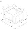
- FIG. 1 is an example of a perspective view showing an external shape of a multilayer ceramic capacitor according to a first embodiment.
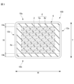
- 1 is a cross-sectional view illustrating a schematic internal structure of a multilayer ceramic capacitor according to a first embodiment.
- 1 is a cross-sectional view illustrating a schematic internal structure of a multilayer ceramic capacitor according to a first embodiment.
- 6 is a perspective view showing another example of the outer shape of the multilayer ceramic capacitor according to the second embodiment.
- present embodiment A specific embodiment of the present invention (hereinafter referred to as the "present embodiment") will be described. Note that the present invention is not limited to the following embodiment, and various modifications are possible without departing from the gist of the present invention.
- the multilayer ceramic capacitor in the first aspect of this embodiment has an internal layer portion, a first external layer portion, a second external layer portion, and a pair of external end surface electrodes.
- the internal layer portion is a region in which the first internal electrode layers and the second internal electrode layers are alternately laminated with a dielectric layer formed of a ceramic dielectric interposed therebetween.
- the internal layer portion has a first main surface, a second main surface, a first side surface, a second side surface, a first end surface, and a second end surface.
- the first main surface is a surface in the lamination direction of the dielectric layer, the first internal electrode layers, and the second electrode layers.
- the second main surface is a surface opposite to the first main surface.
- the first side surface is a surface in the width direction perpendicular to the first main surface and the second main surface.
- the second side surface is a surface opposite to the first side surface.
- the first end surface is a surface in the length direction perpendicular to the first main surface, the second main surface, the first side surface, and the second side surface.
- the second end surface is a surface opposite to the first end surface.
- the first internal electrode layer is drawn out to the first end surface.
- the second internal electrode layer is drawn out to the second end surface.
- the first external layer portion is formed of a ceramic dielectric and covers the first main surface from the stacking direction.
- the second external layer portion is formed of a ceramic dielectric and covers the second main surface from the stacking direction.
- a pair of external end surface electrodes is provided on the first end surface and the second end surface, and is connected to the first internal electrode layer and the second internal electrode layer, respectively.
- Each of the ceramic dielectrics constituting the internal layer portion, the first external layer portion, and the second external layer portion has a plurality of dielectric particles having voids therein.
- the intragranular void ratio (N inner ) of the ceramic dielectric in the internal layer portion and the intragranular void ratio (N outer ) of the ceramic dielectric in the first external layer portion and the second external layer portion satisfy the formula (1): N outer ⁇ N inner .
- the multilayer ceramic capacitor in the second aspect of the present embodiment has an inner layer portion, a first outer layer portion, a second outer layer portion, a pair of outer end surface electrodes, and a pair of outer side surface electrodes.
- the inner layer portion is a region in which the first inner electrode layers and the second inner electrode layers are alternately laminated with a dielectric layer formed of a ceramic dielectric interposed therebetween.
- the inner layer portion has a first main surface, a second main surface, a first side surface, a second side surface, a first end surface, and a second end surface.
- the first main surface is a surface in the lamination direction of the dielectric layer, the first inner electrode layers, and the second electrode layers.
- the second main surface is a surface opposite to the first main surface.
- the first side surface is a surface in the width direction perpendicular to the first main surface and the second main surface.
- the second side surface is a surface opposite to the first side surface.
- the second inner electrode layer is drawn out to the first side surface and the second side surface.
- the first end surface is a surface in the length direction perpendicular to the first main surface, the second main surface, the first side surface, and the second side surface.
- the second end surface is a surface opposite to the first end surface.
- the first internal electrode layer is drawn out to the first end face and the second end face.
- the first external layer portion is formed of a ceramic dielectric and covers the first main surface from the stacking direction.
- the second external layer portion is formed of a ceramic dielectric and covers the second main surface from the stacking direction.
- a pair of external end face electrodes are provided on the first end face and the second end face, and are connected to the first internal electrode layer.
- a pair of external side surface electrodes are provided on the first side surface and the second side surface, and are connected to the second internal electrode layer.
- Each of the ceramic dielectrics constituting the internal layer portion, the first external layer portion, and the second external layer portion has a plurality of dielectric particles having voids therein.
- the intragranular void ratio (N inner ) of the ceramic dielectric in the internal layer portion and the intragranular void ratio (N outer ) of the ceramic dielectric in the first external layer portion and the second external layer portion satisfy the formula (1): N outer ⁇ N inner .
- Figure 1 is a perspective view showing the external shape of the multilayer ceramic capacitor.
- Figure 2 is a cross-section taken along line II-II of the multilayer ceramic capacitor shown in Figure 1
- Figure 3 is a cross-section taken along line III-III.
- the multilayer ceramic capacitor (100) comprises an element body (6) and a pair of external end electrodes (8a, 8b) provided on both end faces (14a, 14b) of the element body (6).
- the multilayer ceramic capacitor (100) and the element body (6) have an approximately rectangular parallelepiped shape.
- An approximately rectangular parallelepiped includes not only rectangular parallelepipeds, but also rectangular parallelepipeds with rounded corners and/or edges.
- the multilayer ceramic capacitor (100) and the element part (6) have a first outer main surface (10a) and a second outer main surface (10b) that face the thickness direction T, a first outer side surface (12a) and a second outer side surface (12b) that face the width direction W, and a first outer end surface (14a) and a second outer end surface (14b) that face the length direction L.
- the thickness direction T is the direction in which the dielectric layers (2) and the internal electrode layers (4) included in the element part (6) are stacked.
- the length direction L is perpendicular to the thickness direction T and is the direction in which the outer end surfaces (14a, 14b) face each other.
- the width direction W is a direction perpendicular to the thickness direction T and the length direction L.
- a surface including the thickness direction T and the width direction W is defined as a WT surface
- a surface including the width direction W and the length direction L is defined as an LW surface
- a surface including the length direction L and the thickness direction T is defined as an LT surface.
- the body portion (6) is composed of an inner layer portion (16), a first outer layer portion (18a), and a second outer layer portion (18b).
- the inner layer portion (16) is a region in which the internal electrode layers (4) are alternately stacked with the dielectric layers (2) interposed therebetween.
- the dielectric layers (2) are made of a ceramic dielectric.
- the internal electrode layers (4) are composed of a plurality of first internal electrode layers (4a) and a plurality of second internal electrode layers (4b).
- the inner layer portion (16) has a first main surface, a second main surface, a first side surface, a second side surface, a first end surface, and a second end surface.
- the first main surface is a surface perpendicular to the stacking direction of the dielectric layer (2) and the internal electrode layers (4a, 4b).
- the second main surface is a surface (opposing surface) opposite the first main surface.
- the first side surface is a surface perpendicular to the first main surface and the second main surface, i.e., a surface perpendicular to the width direction W.
- the second side surface is a surface (opposing surface) opposite the first side surface.
- the first end surface is a surface perpendicular to the first main surface, the second main surface, the first side surface, and the second side surface, i.e., a surface perpendicular to the length direction L.
- the second end surface is a surface (opposing surface) opposite the first end surface.
- the internal electrode layers (4a, 4b) are not extended to the first side surface and the second side surface.
- the first internal electrode layer (4a) is extended to the first end face, but the second internal electrode layer (4b) is not extended.
- the second internal electrode layer (4b) is extended to the second end face, but the first internal electrode layer (4a) is not extended.
- the first outer layer portion (18a) is a region that covers the first main surface of the inner layer portion (16) from the stacking direction (thickness direction T).
- the second outer layer portion (18b) is a region that covers the second main surface of the inner layer portion (16) from the stacking direction.
- the first outer layer portion (18a) and the second outer layer portion (18b) are formed of a ceramic dielectric.
- the external end surface electrodes (8a, 8b) are composed of a first external end surface electrode (8a) provided on the first external end surface (14a) of the element body (6) and a second external end surface electrode (8b) provided on the second external end surface (14b).
- the first external end surface electrode (8a) is electrically connected to the first internal electrode layer (4a).
- the second external end surface electrode (8b) is electrically connected to the second internal electrode layer (4b).
- the first external end surface electrode (8a) and the second external end surface electrode (8b) are not connected and are electrically separated from each other.
- FIG. 4 shows an external perspective view of the multilayer ceramic capacitor in the second embodiment.
- the multilayer ceramic capacitor in the second embodiment is a so-called three-terminal capacitor that has external electrodes (external end face electrodes, external side face electrodes) on the end faces and side faces.
- external electrodes external end face electrodes, external side face electrodes
- the structure other than the internal electrode layers and external electrodes is the same as in the first embodiment.
- the first internal electrode layer (4a) is extended to the end faces (first end face, second end face) of the inner layer, but is not extended to the side faces (first side face, second side face).
- the second internal electrode layer (4b) is extended to the side faces (first side face, second side face) of the inner layer, but is not extended to the end faces (first end face, second end face).
- a first external end surface electrode (8a) and a second external end surface electrode (8b) are provided on the first external end surface (14a) and the second external end surface (14b) of the element body (6), respectively, and a first external side surface electrode (8c) and a second external side surface electrode (8d) are provided on the first external side surface (12a) and the second external side surface (12b), respectively.
- Both of the external end surface electrodes (8a, 8b) are electrically connected to the first internal electrode layer (4a).
- Both of the external side surfaces electrodes (8c, 8d) are electrically connected to the second internal electrode layer (4b).
- the external end surface electrodes (8a, 8b) and the external side surfaces electrodes (8c, 8d) are not connected and are electrically separated from each other.
- the size of the multilayer ceramic capacitor (100) or the element portion (6) is not particularly limited.
- the lengthwise L dimension is 0.2 mm or more and 3.2 mm or less
- the widthwise W dimension is 0.1 mm or more and 2.5 mm or less
- the stacking direction T dimension is 0.1 mm or more and 2.5 mm or less.
- the lengthwise L dimension is shown to be larger than the widthwise W dimension in Figures 1 to 3, the multilayer ceramic capacitor of this embodiment is not limited to having such dimensions.
- the lengthwise L dimension may be smaller than the widthwise W dimension.
- the inner layer portion is a region in which the internal electrode layers (first internal electrode layer, second internal electrode layer) are alternately laminated via dielectric layers formed of ceramic dielectrics.
- the dielectric layers are made of ceramic dielectrics produced by firing green sheets for the inner layers containing dielectric raw materials.
- the ceramic dielectrics are made of sintered polycrystalline bodies (ceramics) in which a large number of dielectric particles are bonded via grain boundaries and triple junctions. In other words, they contain dielectric particles (dielectric grains) as the main component.
- the main component is the component with the largest content in the ceramic dielectric, i.e., a component that accounts for 50% by mass or more.
- Perovskite oxides have a composition represented by the general formula: ABO3 , and have a cubic-like crystal structure such as a cubic, tetragonal, orthorhombic, or rhombohedral crystal at room temperature.
- A-site element atoms hereinafter, "A-site atoms”
- B-site element atoms hereinafter, "B-site atoms”
- A-site elements include elements with relatively large ion sizes such as barium (Ba), calcium (Ca), and strontium (Sr), and examples of B-site elements include elements with relatively small ion sizes such as titanium (Ti), zirconium (Zr), and hafnium (Hf).
- the combination of A-site elements and B-site elements is not particularly limited as long as the perovskite structure is maintained.
- Each of the A-site elements and B-site elements may include only one type of element, or may include a combination of multiple elements.
- the molar ratio of A-site elements to B-site elements may deviate from 1:1, so long as the perovskite structure is maintained.
- perovskite oxides include barium titanate (BaTiO 3 )-based compounds, calcium titanate (CaTiO 3 )-based compounds, strontium titanate (SrTiO 3 )-based compounds, and mixed crystals and solid solutions thereof.
- the A-site element contains barium (Ba) and the B-site element contains titanium (Ti). That is, the perovskite oxide is preferably a barium titanate (BaTiO 3 )-based compound.
- BaTiO 3 -based compounds include not only BaTiO 3 but also compounds in which part of Ba in BaTiO 3 is replaced with other A-site elements such as Sr and/or Ca, or compounds in which part of Ti is replaced with other B-site elements such as Zr and/or Hf.
- the ceramic dielectric may contain minor components.
- minor components include, but are not limited to, rare earth elements (RE), magnesium (Mg), manganese (Mn), iron (Fe), chromium (Cr), cobalt (Co), nickel (Ni), silicon (Si), aluminum (Al), vanadium (V), and compounds thereof.
- the minor components may contain the above-mentioned components alone or in combination. There are no limitations on the form in which the minor components exist. They may be contained in any of the dielectric particles, grain boundaries, and triple points.
- the dielectric particles may include core-shell particles.
- Core-shell particles are particles having a structure (core-shell structure) in which at least a part of the minor component is dissolved in a high concentration in the surface layer (shell portion) of the particle, and the minor component is dissolved in a low concentration or is not dissolved in the center (core portion) of the particle.
- the dielectric particles may include homogeneous solid solution particles.
- the thickness of the dielectric layer occupying the inner layer is preferably 0.3 ⁇ m or more and 0.5 ⁇ m or less.
- the dielectric layer thicker than a specified value, it is possible to suppress the occurrence of insulation breakdown and deterioration of the life span of the multilayer ceramic capacitor when it is used.
- the dielectric layer thicker than a specified value, the dielectric layer is made thinner, making it possible to further increase the capacity of the multilayer ceramic capacitor.
- the number of dielectric layers constituting the outer layer and inner layer is 100 or more and 2000 or less.
- the internal electrode layers are composed of a counter electrode portion and an extraction electrode portion, and together with the dielectric layer, they constitute the internal layer portion.
- the counter electrode portion sandwiches the dielectric layer and functions as a capacitance element.
- the extraction electrode portion extends to the end face and/or side face of the internal layer portion, and functions to electrically connect the counter electrode portion and the external electrode (external end face electrode, external side face electrode).
- the internal electrode layers contain a conductive metal.
- a known electrode material such as nickel (Ni), copper (Cu), silver (Ag), palladium (Pd), silver (Ag)-palladium (Pd) alloy and/or gold (Au) may be used.
- the internal electrode layers are produced by sintering a conductive paste layer printed on the surface of the internal layer green sheet.
- the internal electrode layer may contain components other than conductive metals. Examples of other components include ceramic components that act as co-materials.
- the thickness of the internal electrode layer is preferably 0.30 ⁇ m or more and 0.40 ⁇ m or less. By making the internal electrode thickness a specified value or more, problems such as electrode breakage can be prevented. By making the thickness less than a specified value, a decrease in the proportion of the dielectric layer in the capacitor can be prevented, which contributes to increased capacity.
- the number of layers of the internal electrode layer is preferably 10 to 1,000.
- the outer layer portions (first outer layer portion, second outer layer portion) are provided above and below the inner layer portion.
- the outer layer portions are made of a ceramic dielectric and are regions that do not include an internal electrode layer therein.
- the outer layer portions are produced by firing an outer layer green sheet that includes a dielectric material.
- the external electrodes function as input/output terminals of the multilayer ceramic capacitor.
- the capacitor of the first embodiment has only external end surface electrodes (first external end surface electrodes, second external end surface electrodes) provided on both end surfaces.
- the capacitor of the second embodiment has external end surface electrodes (first external end surface electrodes, second external end surface electrodes) provided on both end surfaces and external side surface electrodes (first external side surface electrodes, second external side surface electrodes) provided on both side surfaces.
- a known configuration can be adopted for the external electrodes.
- it may include a base electrode layer and a plating layer disposed thereon.
- the external electrodes may be formed only by the plating layer without providing a base electrode layer.
- the ceramic dielectrics constituting the inner layer portion, the first outer layer portion, and the second outer layer portion each have a plurality of dielectric particles having voids therein. That is, these ceramic dielectrics are produced using hydrothermal synthesis dielectric powder.
- the intragranular void ratio (N inner ) of the ceramic dielectric in the inner layer portion (hereinafter, sometimes collectively referred to as "inner layer ceramic") and the intragranular void ratio (N outer ) of the ceramic dielectric in the outer layer portion (first outer layer portion and second outer layer portion) (hereinafter, sometimes collectively referred to as "outer layer ceramic”) satisfy the formula (1): N outer ⁇ N inner .
- the intragranular void ratio is the number of intragranular voids per unit area in a cross section (WT surface) crossing the longitudinal center portion of the multilayer ceramic capacitor.
- intragranular voids are voids present inside the dielectric particles constituting the ceramic dielectric.
- a particle having a void inside is called a particle with a void.
- the inner ceramic layer is a region that functions as a capacitance element.
- intragranular voids are formed by using hydrothermally synthesized dielectric powder as a raw material.
- hydrothermally synthesized dielectric powder it is possible to make the multilayer ceramic capacitor thinner and to increase its capacity.
- particle size variation of the dielectric particles is suppressed, it is possible to improve the dielectric constant and reliability.
- particles having intragranular voids have high crystallinity around the voids, and problems caused by diffusion of minor component elements can be suppressed.
- the dielectric particles are core-shell particles
- the diffusion and solid solution of the minor components do not proceed more than necessary even if the particles are grown in the firing process. Since grain growth is possible without destroying the core-shell structure, it is possible to achieve both a high dielectric constant, flat temperature characteristics, and excellent reliability.
- the intragranular void ratio of the inner layer ceramic is relatively high in order to ensure good products and reliability.
- the intragranular void ratio is preferably 8/ ⁇ m2 or more and 18/ ⁇ m2 or less , and more preferably 11/ ⁇ m2 or more and 18/ ⁇ m2 or less .
- the intragranular void ratio is obtained by observing the cross section (WT surface) crossing the longitudinal center of the multilayer ceramic capacitor with a transmission electron microscope (TEM). Specifically, a TEM observation sample having a thickness of 80 nm including the WT surface is prepared. The obtained sample is observed with a TEM in a 2 ⁇ m square field of view to count the number of intragranular voids.
- the obtained number is then divided by the area of the ceramic part (dielectric layer) to calculate the number per unit area (1 ⁇ m2 ).
- the average pore size of the pores is preferably 10 nm or more and 50 nm or less, and particularly preferably 10 nm or more and 30 nm or less.
- the outer ceramic layers that sandwich the inner ceramic layer from above and below do not function as capacitive elements.
- the outer ceramic layer does not have an internal electrode layer. It is not affected by stress from the internal electrode layer during the firing process in the manufacture of multilayer ceramic capacitors, and therefore tends to have lower sinterability than the inner ceramic layer.
- the outer ceramic layer which has low sinterability, has intragranular voids, moisture from the external environment can easily penetrate through these voids. The penetrated moisture can reach the inner ceramic layer, which functions as a capacitive element, and cause problems such as a decrease in insulation resistance.
- the intragranular porosity ratio of the outer ceramic smaller than that of the inner ceramic layer, it is possible to obtain the effect of improving moisture resistance while ensuring the effect of the intragranular porosity in the inner ceramic layer. Therefore, in this embodiment, it is a requirement to satisfy the formula (1): N outer ⁇ N inner .
- the outer ceramic layer it is effective to provide a certain degree of intragranular voids in the outer ceramic layer, provided that the above formula (1) is satisfied.
- the outer ceramic layer it is necessary to suppress the variation in particle size of the dielectric particles throughout the electrically active inner ceramic layer.
- the outer ceramic layer it is advantageous for the outer ceramic layer to contain some intragranular voids.
- the intragranular void ratio (N outer ) in the outer layer ceramic is preferably 3 voids/ ⁇ m2 or more and 13 voids/ ⁇ m2 or less, and more preferably 3 voids/ ⁇ m2 or more and 11 voids/ ⁇ m2 or less.
- the outer layer ceramic includes a portion corresponding to the first outer layer portion and a portion corresponding to the second outer layer portion.
- the intragranular void ratio of the portion corresponding to the first outer layer portion and the intragranular void ratio of the portion corresponding to the second outer layer portion may be the same or different. As long as both are smaller than the intragranular void ratio of the inner layer ceramic, there are no limitations on the magnitude relationship between the two.
- the zirconium (Zr) concentration (Zr inner ) of the inner layer ceramic and the zirconium (Zr outer ) concentration of the outer layer ceramic satisfy the formula (2): Zr inner ⁇ Zr outer .
- a grain growth promoter such as Zr
- the concentration of the grain growth promoter (Zr, etc.) in the outer layer ceramic is higher than that of the inner layer ceramic.
- the Zr concentration at the location corresponding to the first outer layer portion and the Zr concentration at the location corresponding to the second outer layer portion may be the same or different, as long as both are higher than the Zr concentration of the inner layer ceramic.
- the average particle size (D50 inner ) of the dielectric particles of the inner ceramic layer and the average particle size (D50 outer ) of the dielectric particles of the outer ceramic layer satisfy the formula (3): D50 inner ⁇ D50 outer .
- the intragranular void ratio can be suppressed.
- the average particle size of the portion corresponding to the first outer layer portion and the average particle size of the portion corresponding to the second outer layer portion may be the same or different, as long as they are both larger than the average particle size of the inner ceramic layer.
- the average particle size (D50 inner ) of the dielectric particles of the inner layer ceramic is 130 nm or more and 210 nm or less.
- the average particle size is the average particle size of the entire dielectric particles including not only particles with holes but also particles without holes.
- the multilayer ceramic capacitor of this embodiment is not limited in its manufacturing method as long as it satisfies the above-mentioned requirements.
- a suitable manufacturing method includes the following steps: a step of synthesizing a main component powder for ceramic dielectrics (synthesizing step), a step of mixing a subcomponent raw material with the main component powder to obtain a dielectric raw material (mixing step), a step of adding and mixing a binder and a solvent to the dielectric raw material to form a slurry, and a step of forming an inner layer green sheet and an outer layer green sheet from the obtained slurry (forming step), a step of forming a patterned conductive paste layer on the surface of the inner layer green sheet using an internal electrode conductive paste (printing step), a step of laminating a plurality of inner layer green sheets on which a conductive paste layer is formed, laminating an outer layer green sheet above and below it, and pressing the whole together to produce
- the manufacturing conditions are controlled so that the intragranular porosity ratio (N inner ) of the inner layer ceramic and the intragranular porosity ratio (N outer ) of the outer layer ceramic satisfy the formula (1): N outer ⁇ N inner .
- N inner intragranular porosity ratio
- N outer intragranular porosity ratio
- the main component powder used for forming the ceramic dielectric is synthesized.
- the main component powder is a dielectric powder having a perovskite structure (ABO 3 ) such as BaTiO 3 based compounds.
- a hydrothermally synthesized dielectric powder is used as the main component powder. This makes it possible to manufacture a multilayer ceramic capacitor including dielectric particles having voids inside (particles with voids).
- the main component powder only the hydrothermally synthesized dielectric powder may be used, or a combination of the hydrothermally synthesized dielectric powder and a dielectric powder synthesized by a method other than the hydrothermal method may be used.
- the main component powder after synthesis may be pulverized to adjust the particle size.
- the hydrothermally synthesized dielectric powder can be synthesized by hydrothermally reacting a raw material (A-site raw material) containing an A-site element constituting a perovskite structure and a raw material (B-site raw material) containing a B-site element under high temperature and high pressure. Specifically, the raw material is placed together with water in a sealed container such as an autoclave and heated to cause a hydrothermal reaction.
- A-site raw material a hydroxide such as barium hydroxide (Ba(OH) 2 ) is used.
- an oxide such as titanium oxide (TiO 2 ) or metatitanic acid (TiO(OH) 2 ) or its hydrate is used.
- the heating temperature is not limited, but may be 150° C. or more and 250° C. or less.
- the product obtained by the hydrothermal reaction can be dried to obtain a dielectric powder.
- the product may be subjected to a heat treatment in order to increase the crystallinity of the dielectric powder.
- the heat treatment may be performed at a temperature of, for example, 800° C. or more and 1000° C. or less.
- ⁇ Mixing step> the main component powder is mixed with the auxiliary component (Ni, Re, Mg, Mn, Si, Al, V, etc.) raw material to obtain a dielectric raw material.
- auxiliary component raw material a known ceramic raw material such as an oxide, a carbonate, a hydroxide, a nitrate, an organic acid salt, an alkoxide, and/or a chelate compound may be used.
- a composition control agent for the main component powder may be added.
- the main component powder is barium titanate (BaTiO 3 ) powder
- adding a Ba raw material such as barium carbonate (BaCO 3 ) can control the main component composition of the ceramic dielectric.
- the mixing method is not particularly limited. For example, a method of wet mixing and grinding the weighed main component powder and the auxiliary component raw material together with a grinding medium and pure water using a ball mill can be mentioned. When the wet mixing is performed, the mixture may be dried.
- a binder and a solvent are added to and mixed with the dielectric material to form a slurry, and the resulting slurry is molded into inner layer green sheets and outer layer green sheets.
- a binder a known organic binder such as a polyvinyl butyral binder may be used.
- solvent a known organic solvent such as toluene or ethanol may be used. Additives such as a plasticizer may be added as necessary. Molding may be performed by a known method such as the lip method.
- the sheet thickness after molding is, for example, 1 ⁇ m or less.
- a patterned conductive paste layer is formed on the surface of the inner layer green sheet using a conductive paste.
- the conductive paste layer becomes an internal electrode layer after firing.
- the conductive metal contained in the conductive paste may be nickel (Ni), copper (Cu), silver (Ag), palladium (Pd), or an alloy containing these conductive materials.
- a ceramic component acting as a co-material may also be added to the conductive paste.
- the method of forming the conductive paste layer is not particularly limited. For example, methods such as screen printing and gravure printing may be used.
- ⁇ Lamination process> In the lamination process, multiple inner layer green sheets with conductive paste layers formed thereon are laminated, and outer layer green sheets are laminated above and below them. The whole is then pressed together to create a laminated block.
- the inner layer green sheets undergo a firing process to become the ceramic dielectric (inner layer ceramic) that constitutes the inner layer portion of the multilayer ceramic capacitor.
- the outer layer green sheets become the ceramic dielectric (outer layer ceramic) that constitutes the outer layer portion.
- the number of green sheets to be laminated can be adjusted to obtain the required capacity.
- the obtained laminated block is cut to obtain laminated chips.
- the cutting may be performed so that chips of a predetermined size are obtained and a part of the conductive paste layer is exposed on an end face of the laminated chip.
- the cutting may be performed so that a part of the conductive paste layer is exposed on a side face of the laminated chip.
- the resulting laminated chip may be subjected to a barrel polishing process. This process makes it possible to round the corners and/or edges of the green body.
- the laminated chip is subjected to a binder removal process and a firing process to obtain an element part.
- the firing process causes the conductive paste layer and the inner layer green sheet to be co-sintered to become the internal electrode layer and ceramic dielectric that constitute the inner layer part.
- the outer layer green sheet is sintered to become the ceramic dielectric that constitutes the outer layer part.
- the conditions of the binder removal process may be determined according to the type of organic binder contained in the green sheet and the conductive paste layer.
- the firing process may be performed at a temperature at which the laminated chip is sufficiently densified. For example, the firing process may be performed under conditions of holding the temperature at 1200°C or higher and 1300°C or lower for 0 minutes or longer and 10 minutes or shorter.
- the firing process may be performed in an atmosphere in which the main component compound such as BaTiO 3 is not reduced and the oxidation of the conductive material is suppressed.
- the firing process may be performed in a N 2 -H 2 -H 2 O air flow with an oxygen partial pressure of 1.8 ⁇ 10 -9 to 8.7 ⁇ 10 -10 MPa.
- an annealing process may be performed after the firing process.
- external electrodes (external end surface electrodes, external side surface electrodes) are formed on the element part to fabricate a multilayer ceramic capacitor.
- the external electrodes may be formed by a known method. For example, a conductive paste mainly composed of a conductive component such as Cu or Ni is applied and baked on the end surface and/or side surface exposed by drawing out the internal electrode layer of the element part to form a base layer.
- the base layer may be formed by applying a conductive paste to both end surfaces of the green element part before firing and then performing a firing process. After forming the base layer, electrolytic plating may be performed to form a plating film of Ni, Sn, or the like on the surface of the base layer. In this way, a multilayer ceramic capacitor is fabricated.
- the method of controlling the intragranular void ratio is not limited.
- a method of adding a grain growth promoter or a grain growth inhibitor to the main component powder and adjusting the amount of the promoter can be used.
- grain growth promoters include zirconium (Zr), silicon (Si), vanadium (V), and/or aluminum (Al). Dielectric particles grow during the firing process. As the grain growth progresses, the intragranular voids become smaller and may disappear. Therefore, if a grain growth promoter is added to the outer layer green sheet in a larger amount than the inner layer green sheet, the intragranular void ratio of the outer layer ceramic can be reduced. In that case, in the final multilayer ceramic capacitor, the concentration of the grain growth promoter (Zr, etc.) in the outer layer ceramic will be higher than that in the inner layer ceramic.
- the main component powder is a perovskite oxide having a composition represented by the formula ABO3 , such as BaTiO3 .
- ABO3 such as BaTiO3
- Another method is to adjust the particle size of raw material particles such as the main component powder.
- Another method is to add a dielectric powder synthesized by a method other than the hydrothermal method, for example a solid-phase method, to the main component powder.
- a dielectric powder synthesized by a method other than the hydrothermal method for example a solid-phase method
- hydrothermally synthesized dielectric powder has intragranular voids
- dielectric powder synthesized by a method other than the hydrothermal method does not have intragranular voids. Therefore, by using hydrothermally synthesized dielectric powder in combination with a dielectric powder synthesized by a method other than the hydrothermal method, the intragranular void ratio can be controlled.
- one method is to produce an inner layer green sheet from hydrothermally synthesized dielectric powder, while producing an outer layer green sheet from a mixed powder of hydrothermally synthesized dielectric powder and dielectric powder synthesized by a solid-phase method.
- the intragranular void ratios of the inner and outer ceramic layers can be controlled to satisfy a specified relationship, there are no limitations on the method for controlling the intragranular void ratio.
- Example 1 (1) Fabrication of Multilayer Ceramic Capacitor [Example 1]
- inner layer green sheets and outer layer green sheets were prepared using a barium titanate (BaTiO 3 ) powder synthesized by a hydrothermal method as a main component powder, and a multilayer ceramic capacitor was prepared using these.
- the specific preparation procedure is shown below.
- Barium titanate (BaTiO 3 ) powder was synthesized by hydrothermal method. First, titanium oxide (TiO 2 ) powder and barium hydroxide (Ba(OH) 2 ) powder were weighed, and pure water was added to prepare a slurry. The prepared slurry was then placed in a sealed container, and the temperature of the slurry was raised to 200-250°C while stirring. The temperature was then kept at 200-250°C for 4-24 hours to allow the liquid phase reaction to proceed. After that, the internal pressure of the sealed container was returned to atmospheric pressure, heating of the sealed container was stopped, and the slurry was left as it was. After cooling, the slurry was removed from the sealed container and placed in a dryer to evaporate the water. In this way, hydrothermally synthesized BaTiO 3 powder with an average particle size of 130 nm was obtained.
- a polyvinyl butyral binder and ethanol as an organic solvent were added to the obtained dielectric raw material, and the mixture was wet-mixed by a ball mill for a predetermined time to prepare a slurry. This slurry was formed into a sheet to prepare an inner layer green sheet.
- a polyvinyl butyral binder and ethanol, an organic solvent were added to the obtained dielectric raw material, and the mixture was wet-mixed by a ball mill for a predetermined time to prepare a slurry.
- This slurry was formed into a sheet to prepare an outer layer green sheet.
- a conductive paste mainly made of Ni was screen-printed on the surface of the obtained green sheet for the inner layer, and a conductive paste layer that would become an internal electrode layer was patterned. Then, a plurality of green sheets for the inner layer on which the conductive paste layer was formed were stacked, and green sheets for the outer layer on which the conductive paste layer was not formed were placed above and below them, and the whole was pressed together to produce a laminated block. The obtained laminated block was then cut with a dicing saw to form a laminated chip. The stacking was performed so that the ends from which the conductive paste layer was drawn out were staggered. The cutting was also performed so that the drawn-out parts of the conductive paste layer were exposed on the end faces.
- the obtained laminated chip was heat-treated in an N2 gas flow at a maximum temperature of 270°C, and further heat-treated in an N2 - H2O - H2 gas flow at a maximum temperature of 800°C. Then, it was sintered in an N2 - H2O - H2 gas flow. The sintering was performed under the conditions of a maximum temperature of 1230-1400°C, a temperature rise rate of 20-60°C/min, a hold time of 60 minutes, and an oxygen partial pressure of 5.0x10⁻¹³ to 1.7x10⁻¹² MPa. Next, it was heat-treated in an N2 - H2O - H2 gas flow at a maximum temperature of 1050°C for 60 minutes. This resulted in the formation of an element part.
- a conductive paste mainly composed of copper (Cu) was applied to the end faces of the element part obtained by firing, from which the internal electrode layers were drawn out.
- the applied conductive paste was then baked at 900°C to form a base layer for the external electrodes (external end surface electrodes).
- Ni plating and Sn plating were applied, in that order, to the surface of the base layer by wet plating. In this way, a multilayer ceramic capacitor was produced.
- the multilayer ceramic capacitor thus produced had a length L dimension of 1.0 mm, a width W dimension of 0.5 mm, and a thickness T dimension of 0.5 mm.
- the thickness of the dielectric layer in the inner layer was 0.49 ⁇ m
- the thickness of the internal electrode layer was 0.44 ⁇ m
- the number of dielectric layers was 470.
- Example 2 when preparing the green sheets for the inner layers, hydrothermally synthesized BaTiO3 powder (average particle size 80 nm) was used instead of hydrothermally synthesized BaTiO3 powder (average particle size 130 nm). Except for this, a multilayer ceramic capacitor was prepared in the same manner as in Example 1. The hydrothermally synthesized BaTiO3 powder (average particle size 80 nm) was synthesized in the same manner as the hydrothermally synthesized BaTiO3 powder (average particle size 130 nm) except that the slurry temperature during hydrothermal synthesis was lowered.
- Example 3 In Example 3, ZrO2 was not added when preparing the ceramic green sheets for the outer layer. The amount of BaCO3 added was adjusted so that the molar ratio (Ba/Ti ratio) of the outer layer ceramic was 1.0000. A multilayer ceramic capacitor was prepared in the same manner as in Example 1 except for the above.
- Example 4 In Example 4, the amount of ZrO2 added when preparing the outer layer ceramic green sheets was changed from 0.3 mass% to 0.5 mass%. Otherwise, a multilayer ceramic capacitor was prepared in the same manner as in Example 1.
- Example 5 In Example 5, the grinding time during preparation of the outer layer ceramic green sheets was changed from 24 hours to 48 hours, and ZrO2 was not added. Except for this, a multilayer ceramic capacitor was prepared in the same manner as in Example 1.
- Example 6 In Example 6, a multilayer ceramic capacitor was fabricated in the same manner as in Example 1.
- Example 7 In Example 7, ZrO2 was added together with BaCO3 when preparing the ceramic green sheets for the inner layer, and the amount of ZrO2 added ( ZrO2 added amount) was 0.1 mass% relative to the BaTiO3 powder.
- a multilayer ceramic capacitor was prepared in the same manner as in Example 1 except for the above.
- Example 8 when preparing the ceramic green sheets for the outer layer, a mixed powder containing 70% by mass of hydrothermally synthesized BaTiO3 powder (average particle size 130 nm) and 30% by mass of solid-phase synthesized BaTiO3 powder (average particle size 130 nm) was used as the main component powder. In addition, the amount of BaCO3 added when preparing the ceramic green sheets for the outer layer was adjusted so that the molar ratio (Ba/Ti ratio) of the outer layer ceramic was 1.0050. Otherwise, a multilayer ceramic capacitor was prepared in the same manner as in Example 1.
- Example 9 when preparing the ceramic green sheets for the outer layer, a mixed powder containing 85% by mass of hydrothermally synthesized BaTiO3 powder (average particle size 130 nm) and 15% by mass of solid-phase synthesized BaTiO3 powder (average particle size 130 nm) was used as the main component powder. In addition, no ZrO2 was added when preparing the ceramic green sheets for the outer layer. Furthermore, the amount of BaCO3 added was adjusted so that the molar ratio (Ba/Ti ratio) of the outer layer ceramic was 1.0050. Otherwise, a multilayer ceramic capacitor was prepared in the same manner as in Example 1.
- Example 10 ZrO2 was added together with BaCO3 when preparing the ceramic green sheets for the inner layer, and the amount of ZrO2 added ( ZrO2 added amount) was 0.1 mass% relative to the BaTiO3 powder. In addition, ZrO2 was not added when preparing the ceramic green sheets for the outer layer. Furthermore, the amount of BaCO3 added was adjusted so that the molar ratio (Ba/Ti ratio) of the outer layer ceramic was 1.0000.
- a multilayer ceramic capacitor was prepared in the same manner as in Example 1 except for the above.
- Comparative Example 1 In Comparative Example 1, when preparing the ceramic green sheets for the inner layer, a mixed powder containing 10 mass% of hydrothermally synthesized BaTiO3 powder (average particle size 130 nm) and 90 mass% of solid-phase synthesized BaTiO3 powder (average particle size 130 nm) was used as the main component powder. In addition, the grinding time when preparing the ceramic green sheets for the outer layer was changed from 24 hours to 12 hours, and ZrO2 was not added. Otherwise, a multilayer ceramic capacitor was prepared in the same manner as in Example 1.
- Comparative Example 2 In Comparative Example 2, the grinding time during preparation of the outer layer ceramic green sheets was changed from 24 hours to 12 hours, and ZrO2 was not added. Except for this, a multilayer ceramic capacitor was prepared in the same manner as in Example 1.
- the WT surface of the multilayer ceramic capacitor was observed using a transmission electron microscope (TEM) to examine the intragranular void ratio. Specifically, the multilayer ceramic capacitor was polished to the center in the length direction to expose the WT surface, and further processed to prepare a TEM observation sample with a thickness of 80 nm including the WT surface. Then, the obtained sample was observed with a TEM. At this time, the cross section was divided into an inner layer part and an outer layer part, and the ceramic dielectric part near the center in the W direction and the T direction of the inner layer part, and the ceramic dielectric part near the center in the W direction and the T direction of the outer layer part were observed.
- TEM transmission electron microscope
- the number of voids present in the dielectric particles was counted, and the obtained number was divided by the area of the ceramic part to calculate the number per unit area (1 ⁇ m 2 ).
- the ceramic dielectric that makes up the side margin has a composition and/or microstructure that is continuous with the ceramic dielectric that makes up the inner layer. In other words, there is no physical or chemical boundary between the side margin and the inner layer.
- the intragranular void ratio in the side margin is the same as the intragranular void ratio in the center of the inner layer, or is slightly lower as the grains grow.
- the WT surface of the multilayer ceramic capacitor was observed using a scanning electron microscope (SEM) to examine the thickness of the dielectric layer and the particle size (D50) of the dielectric particles.
- SEM scanning electron microscope
- the multilayer ceramic capacitor was polished to the center in the length (L) direction to expose the cross section (WT surface).
- the thickness of the dielectric layer of the inner layer located near the center in the thickness direction was measured on a total of five lines, including the center line in the width direction W and two lines drawn equally spaced on both sides from this center line toward the width direction W, and the average value was taken as the thickness of the dielectric layer.
- the SEM image of the dielectric particles in the dielectric layer in the exposed cross section was taken under the conditions of 5000 times magnification, 15 kV acceleration voltage, and 30 ⁇ m ⁇ 30 ⁇ m field of view.
- the ceramic dielectric near the center of the inner layer part in the W direction and T direction was taken.
- the edges of all the dielectric particles were recognized using image processing software to calculate the cross-sectional area of the particles, and the circle equivalent diameter was calculated from this area as the diameter of the particle.
- the diameters of all the dielectric particles included in the imaged range were measured, excluding the dielectric particles that were missing, and the average value was calculated to obtain the average particle diameter (D50 inner ) of the dielectric particles in the inner layer ceramic.
- the center of the outer layer part in the W direction and T direction was taken, and the average particle diameter (D50 outer ) of the dielectric particles in the outer layer ceramic was obtained.
- ⁇ Moisture resistance load test> A moisture resistance load test was conducted for 100 samples under conditions of 85°C, 85% relative humidity, and 6.3V. After 250 hours, 500 hours, or 1000 hours, the samples were removed from the test tank and a voltage of 6.3V was applied to them at room temperature for 60 seconds to measure the insulation resistance (IR). Then, LogIR>4 was used as the standard, and samples that all met the standard were judged as pass ( ⁇ ), and samples that had at least one LogIR ⁇ 4 were judged as fail ( ⁇ ). Furthermore, the results of the moisture resistance test were judged according to the following criteria.
- Example 1 the intragranular porosity in the outer layer (N outer ) was smaller than the intragranular porosity in the inner layer (N inner ). Therefore, the results of the moisture resistance load test were good, and the test passed after 250 hours. In particular, Examples 1, 2, and 4 to 7 showed particularly good results in the moisture resistance load test, and the test passed even after 1000 hours.
- Example 8 which has a relatively high molar ratio, had relatively low moisture resistance and the moisture load test result was "Good”.
- Examples 3 and 10 which have a relatively low Zr content, also had relatively low moisture resistance and the moisture load test result was "Good”.
- Example 9 also had a moisture load test result of "Good”, but the molar ratio was high and the Zr content was low. Therefore, although it passed after 250 hours, it failed after 500 hours.
- the multilayer ceramic capacitors of Comparative Examples 1 and 2 had a larger intragranular porosity (N outer ) in the outer layer portion than the intragranular porosity (N inner ) in the inner layer portion, and therefore showed poor results in the humidity resistance load test, failing after 250 hours.
- this embodiment provides a multilayer ceramic capacitor that is particularly excellent in terms of moisture resistance.
- the above describes an embodiment of the present invention, but the present invention is not limited to the embodiment, and can be implemented in various forms without departing from the gist of the present invention.
- the present invention includes the following combinations.
- ⁇ 3> The multilayer ceramic capacitor according to ⁇ 1> or ⁇ 2> above, wherein a Zr concentration (Zr inner ) of the ceramic dielectric in the inner layer portion and a Zr concentration (Zr outer ) of the ceramic dielectric in the first outer layer portion and the second outer layer portion satisfy formula (2): Zr inner ⁇ Zr outer .
Landscapes
- Engineering & Computer Science (AREA)
- Power Engineering (AREA)
- Manufacturing & Machinery (AREA)
- Microelectronics & Electronic Packaging (AREA)
- Ceramic Engineering (AREA)
- Chemical & Material Sciences (AREA)
- Inorganic Chemistry (AREA)
- Ceramic Capacitors (AREA)
- Fixed Capacitors And Capacitor Manufacturing Machines (AREA)
Priority Applications (4)
| Application Number | Priority Date | Filing Date | Title |
|---|---|---|---|
| CN202480054988.1A CN121866637A (zh) | 2023-08-28 | 2024-08-27 | 层叠陶瓷电容器 |
| JP2025543487A JPWO2025047708A1 (https=) | 2023-08-28 | 2024-08-27 | |
| KR1020267005684A KR20260040649A (ko) | 2023-08-28 | 2024-08-27 | 적층 세라믹 콘덴서 |
| US19/295,829 US20250364182A1 (en) | 2023-08-28 | 2025-08-11 | Multilayer ceramic capacitor |
Applications Claiming Priority (2)
| Application Number | Priority Date | Filing Date | Title |
|---|---|---|---|
| JP2023137936 | 2023-08-28 | ||
| JP2023-137936 | 2023-08-28 |
Related Child Applications (1)
| Application Number | Title | Priority Date | Filing Date |
|---|---|---|---|
| US19/295,829 Continuation US20250364182A1 (en) | 2023-08-28 | 2025-08-11 | Multilayer ceramic capacitor |
Publications (1)
| Publication Number | Publication Date |
|---|---|
| WO2025047708A1 true WO2025047708A1 (ja) | 2025-03-06 |
Family
ID=94819165
Family Applications (1)
| Application Number | Title | Priority Date | Filing Date |
|---|---|---|---|
| PCT/JP2024/030407 Pending WO2025047708A1 (ja) | 2023-08-28 | 2024-08-27 | 積層セラミックコンデンサ |
Country Status (5)
| Country | Link |
|---|---|
| US (1) | US20250364182A1 (https=) |
| JP (1) | JPWO2025047708A1 (https=) |
| KR (1) | KR20260040649A (https=) |
| CN (1) | CN121866637A (https=) |
| WO (1) | WO2025047708A1 (https=) |
Citations (8)
| Publication number | Priority date | Publication date | Assignee | Title |
|---|---|---|---|---|
| JPH0354142A (ja) * | 1989-07-21 | 1991-03-08 | Nkk Corp | 異常粒成長を利用した磁器製造法 |
| JP2005159056A (ja) * | 2003-11-26 | 2005-06-16 | Kyocera Corp | 積層セラミック電子部品 |
| JP2016082186A (ja) * | 2014-10-22 | 2016-05-16 | 株式会社村田製作所 | 積層セラミックコンデンサ、これを含む積層セラミックコンデンサ連、および、積層セラミックコンデンサの実装体 |
| JP2018181956A (ja) * | 2017-04-06 | 2018-11-15 | 株式会社村田製作所 | 積層セラミックコンデンサ |
| JP2019102655A (ja) * | 2017-12-04 | 2019-06-24 | 太陽誘電株式会社 | セラミックコンデンサおよびその製造方法 |
| JP2020057738A (ja) * | 2018-10-04 | 2020-04-09 | 株式会社村田製作所 | 電子部品、回路基板、および電子部品の回路基板への実装方法 |
| JP2020191330A (ja) * | 2019-05-20 | 2020-11-26 | 太陽誘電株式会社 | 積層セラミック電子部品及び積層セラミック電子部品の製造方法 |
| JP2022060476A (ja) * | 2018-05-09 | 2022-04-14 | 太陽誘電株式会社 | 積層セラミックコンデンサ及びその製造方法 |
-
2024
- 2024-08-27 JP JP2025543487A patent/JPWO2025047708A1/ja active Pending
- 2024-08-27 WO PCT/JP2024/030407 patent/WO2025047708A1/ja active Pending
- 2024-08-27 CN CN202480054988.1A patent/CN121866637A/zh active Pending
- 2024-08-27 KR KR1020267005684A patent/KR20260040649A/ko active Pending
-
2025
- 2025-08-11 US US19/295,829 patent/US20250364182A1/en active Pending
Patent Citations (8)
| Publication number | Priority date | Publication date | Assignee | Title |
|---|---|---|---|---|
| JPH0354142A (ja) * | 1989-07-21 | 1991-03-08 | Nkk Corp | 異常粒成長を利用した磁器製造法 |
| JP2005159056A (ja) * | 2003-11-26 | 2005-06-16 | Kyocera Corp | 積層セラミック電子部品 |
| JP2016082186A (ja) * | 2014-10-22 | 2016-05-16 | 株式会社村田製作所 | 積層セラミックコンデンサ、これを含む積層セラミックコンデンサ連、および、積層セラミックコンデンサの実装体 |
| JP2018181956A (ja) * | 2017-04-06 | 2018-11-15 | 株式会社村田製作所 | 積層セラミックコンデンサ |
| JP2019102655A (ja) * | 2017-12-04 | 2019-06-24 | 太陽誘電株式会社 | セラミックコンデンサおよびその製造方法 |
| JP2022060476A (ja) * | 2018-05-09 | 2022-04-14 | 太陽誘電株式会社 | 積層セラミックコンデンサ及びその製造方法 |
| JP2020057738A (ja) * | 2018-10-04 | 2020-04-09 | 株式会社村田製作所 | 電子部品、回路基板、および電子部品の回路基板への実装方法 |
| JP2020191330A (ja) * | 2019-05-20 | 2020-11-26 | 太陽誘電株式会社 | 積層セラミック電子部品及び積層セラミック電子部品の製造方法 |
Also Published As
| Publication number | Publication date |
|---|---|
| US20250364182A1 (en) | 2025-11-27 |
| CN121866637A (zh) | 2026-04-14 |
| JPWO2025047708A1 (https=) | 2025-03-06 |
| KR20260040649A (ko) | 2026-03-25 |
Similar Documents
| Publication | Publication Date | Title |
|---|---|---|
| JP7274372B2 (ja) | セラミック電子部品およびその製造方法 | |
| KR102520018B1 (ko) | 적층 세라믹 콘덴서 및 그 제조 방법 | |
| KR102412983B1 (ko) | 적층 세라믹 콘덴서 및 그 제조 방법 | |
| JP2022057629A (ja) | 積層セラミックコンデンサ | |
| TWI793148B (zh) | 積層陶瓷電容器及其製造方法 | |
| KR102163417B1 (ko) | 적층 세라믹 커패시터 | |
| JP6986360B2 (ja) | 積層セラミックコンデンサおよびその製造方法 | |
| JP2026026386A (ja) | セラミック電子部品およびその製造方法 | |
| JP2023003944A (ja) | 誘電体、積層セラミックコンデンサ、誘電体の製造方法、および積層セラミックコンデンサの製造方法 | |
| US10879002B2 (en) | Ceramic capacitor and manufacturing method thereof | |
| KR20230120997A (ko) | 유전체 조성물, 적층 세라믹 전자 부품, 유전체 조성물의 제조 방법, 및 적층 세라믹 전자 부품의 제조 방법 | |
| CN114907114A (zh) | 电介质组合物、电子部件及层叠电子部件 | |
| JP7441110B2 (ja) | 誘電体、電子部品、および積層セラミックコンデンサ | |
| JP2021141131A (ja) | セラミック電子部品の製造方法、および金属導電ペースト | |
| JP2024093966A (ja) | 積層セラミック電子部品、および積層セラミック電子部品の製造方法 | |
| US20240170220A1 (en) | Multilayer ceramic capacitor | |
| JP7683696B2 (ja) | 積層セラミックコンデンサ | |
| WO2025047708A1 (ja) | 積層セラミックコンデンサ | |
| KR20230127904A (ko) | 유전체 조성물, 적층 세라믹 전자 부품 및 적층 세라믹 전자 부품의 제조 방법 | |
| WO2025047707A1 (ja) | 積層セラミックコンデンサ | |
| US20250385046A1 (en) | Multilayer ceramic capacitor | |
| JP7602306B2 (ja) | 粉末材料、ペースト材料、およびセラミック電子部品の製造方法 | |
| WO2024070416A1 (ja) | セラミック電子部品、およびセラミック電子部品の製造方法 | |
| JP2025154091A (ja) | セラミック電子部品 | |
| WO2024247128A1 (ja) | 積層セラミックコンデンサ |
Legal Events
| Date | Code | Title | Description |
|---|---|---|---|
| 121 | Ep: the epo has been informed by wipo that ep was designated in this application |
Ref document number: 24859740 Country of ref document: EP Kind code of ref document: A1 |
|
| ENP | Entry into the national phase |
Ref document number: 2025543487 Country of ref document: JP Kind code of ref document: A |
|
| WWE | Wipo information: entry into national phase |
Ref document number: 2025543487 Country of ref document: JP |
|
| ENP | Entry into the national phase |
Ref document number: 1020267005684 Country of ref document: KR Free format text: ST27 STATUS EVENT CODE: A-0-1-A10-A15-NAP-PA0105 (AS PROVIDED BY THE NATIONAL OFFICE) |