WO2025047665A1 - 光電変換素子、正孔輸送促進材料、および化合物 - Google Patents
光電変換素子、正孔輸送促進材料、および化合物 Download PDFInfo
- Publication number
- WO2025047665A1 WO2025047665A1 PCT/JP2024/030239 JP2024030239W WO2025047665A1 WO 2025047665 A1 WO2025047665 A1 WO 2025047665A1 JP 2024030239 W JP2024030239 W JP 2024030239W WO 2025047665 A1 WO2025047665 A1 WO 2025047665A1
- Authority
- WO
- WIPO (PCT)
- Prior art keywords
- group
- ring
- carbon atoms
- hole transport
- formula
- Prior art date
- Legal status (The legal status is an assumption and is not a legal conclusion. Google has not performed a legal analysis and makes no representation as to the accuracy of the status listed.)
- Ceased
Links
Images
Classifications
-
- C—CHEMISTRY; METALLURGY
- C07—ORGANIC CHEMISTRY
- C07D—HETEROCYCLIC COMPOUNDS
- C07D471/00—Heterocyclic compounds containing nitrogen atoms as the only ring hetero atoms in the condensed system, at least one ring being a six-membered ring with one nitrogen atom, not provided for by groups C07D451/00 - C07D463/00
- C07D471/12—Heterocyclic compounds containing nitrogen atoms as the only ring hetero atoms in the condensed system, at least one ring being a six-membered ring with one nitrogen atom, not provided for by groups C07D451/00 - C07D463/00 in which the condensed system contains three hetero rings
- C07D471/16—Peri-condensed systems
-
- H—ELECTRICITY
- H10—SEMICONDUCTOR DEVICES; ELECTRIC SOLID-STATE DEVICES NOT OTHERWISE PROVIDED FOR
- H10K—ORGANIC ELECTRIC SOLID-STATE DEVICES
- H10K30/00—Organic devices sensitive to infrared radiation, light, electromagnetic radiation of shorter wavelength or corpuscular radiation
- H10K30/30—Organic devices sensitive to infrared radiation, light, electromagnetic radiation of shorter wavelength or corpuscular radiation comprising bulk heterojunctions, e.g. interpenetrating networks of donor and acceptor material domains
-
- H—ELECTRICITY
- H10—SEMICONDUCTOR DEVICES; ELECTRIC SOLID-STATE DEVICES NOT OTHERWISE PROVIDED FOR
- H10K—ORGANIC ELECTRIC SOLID-STATE DEVICES
- H10K30/00—Organic devices sensitive to infrared radiation, light, electromagnetic radiation of shorter wavelength or corpuscular radiation
- H10K30/60—Organic devices sensitive to infrared radiation, light, electromagnetic radiation of shorter wavelength or corpuscular radiation in which radiation controls flow of current through the devices, e.g. photoresistors
-
- H—ELECTRICITY
- H10—SEMICONDUCTOR DEVICES; ELECTRIC SOLID-STATE DEVICES NOT OTHERWISE PROVIDED FOR
- H10K—ORGANIC ELECTRIC SOLID-STATE DEVICES
- H10K30/00—Organic devices sensitive to infrared radiation, light, electromagnetic radiation of shorter wavelength or corpuscular radiation
- H10K30/80—Constructional details
- H10K30/84—Layers having high charge carrier mobility
- H10K30/86—Layers having high hole mobility, e.g. hole-transporting layers or electron-blocking layers
-
- H—ELECTRICITY
- H10—SEMICONDUCTOR DEVICES; ELECTRIC SOLID-STATE DEVICES NOT OTHERWISE PROVIDED FOR
- H10K—ORGANIC ELECTRIC SOLID-STATE DEVICES
- H10K39/00—Integrated devices, or assemblies of multiple devices, comprising at least one organic radiation-sensitive element covered by group H10K30/00
- H10K39/30—Devices controlled by radiation
- H10K39/32—Organic image sensors
-
- H—ELECTRICITY
- H10—SEMICONDUCTOR DEVICES; ELECTRIC SOLID-STATE DEVICES NOT OTHERWISE PROVIDED FOR
- H10K—ORGANIC ELECTRIC SOLID-STATE DEVICES
- H10K50/00—Organic light-emitting devices
- H10K50/10—OLEDs or polymer light-emitting diodes [PLED]
- H10K50/14—Carrier transporting layers
- H10K50/15—Hole transporting layers
-
- H—ELECTRICITY
- H10—SEMICONDUCTOR DEVICES; ELECTRIC SOLID-STATE DEVICES NOT OTHERWISE PROVIDED FOR
- H10K—ORGANIC ELECTRIC SOLID-STATE DEVICES
- H10K85/00—Organic materials used in the body or electrodes of devices covered by this subclass
- H10K85/60—Organic compounds having low molecular weight
-
- Y—GENERAL TAGGING OF NEW TECHNOLOGICAL DEVELOPMENTS; GENERAL TAGGING OF CROSS-SECTIONAL TECHNOLOGIES SPANNING OVER SEVERAL SECTIONS OF THE IPC; TECHNICAL SUBJECTS COVERED BY FORMER USPC CROSS-REFERENCE ART COLLECTIONS [XRACs] AND DIGESTS
- Y02—TECHNOLOGIES OR APPLICATIONS FOR MITIGATION OR ADAPTATION AGAINST CLIMATE CHANGE
- Y02E—REDUCTION OF GREENHOUSE GAS [GHG] EMISSIONS, RELATED TO ENERGY GENERATION, TRANSMISSION OR DISTRIBUTION
- Y02E10/00—Energy generation through renewable energy sources
- Y02E10/50—Photovoltaic [PV] energy
- Y02E10/549—Organic PV cells
Definitions
- the present invention relates to a photoelectric conversion element, a hole transport promoting material, and a compound.
- organic electronic elements such as photoelectric conversion elements and organic EL elements
- material and device design aimed at improving device performance.
- photoelectric conversion elements used for video recording if the speed at which carriers (electrons and holes) generated in the light-receiving layer are transported to the electrode is slow, this can cause afterimages.
- organic EL elements if the speed at which carriers are transported from the electrode to the light-emitting layer is slow, this can cause the driving voltage to increase. Therefore, in order to improve the performance of devices, highly efficient movement of carriers within the element is required.
- Patent Document 1 it has been disclosed that a compound having an imide structure can be used in the electron transport layer of an organic thin-film solar cell (see Patent Document 1), but further improvements are needed to achieve this in the field of organic electronic devices, which demands even greater performance.
- the object of the present invention is to provide a photoelectric conversion element capable of improving the hole transport capacity, and a hole transport promotion material and compound capable of improving the hole transport capacity.
- the inventors conducted extensive research to solve the above problems and discovered that it is possible to improve the hole transport capacity in a photoelectric conversion element that includes a hole transport promotion layer containing a compound of the specific structure shown below, or that includes a layer in which a hole transport material is mixed with the compound, thereby completing the present invention.
- a photoelectric conversion element including a first electrode, a second electrode, and a light receiving layer and an organic layer disposed between the first electrode and the second electrode,
- the organic layer includes a hole transport layer and a hole transport promoting layer containing a compound represented by the following formula (1), or includes a layer formed by mixing a hole transport material and a compound represented by the following formula (1): Photoelectric conversion element.
- Ring A represents an optionally substituted aromatic hydrocarbon ring having 6 to 20 carbon atoms (which may be a monocyclic ring, a condensed ring, or a linked ring containing a plurality of rings);
- Ring B represents an imidazole ring or a fused imidazole ring having 5 to 20 carbon atoms;
- R 1 each independently represents a hydroxyl group, a carboxyl group, a formyl group, an acyl group, a nitro group, a cyano group, a fluorine atom, a chlorine atom, a bromine atom, an iodine atom, a trifluoromethyl group, a methyl group, a fluoroalkyl group having 2 to 10 carbon atoms, a fluoroalkoxy group having 1 to 10 carbon atoms, an alkyl group having 2 to 10 carbon atoms, an aromatic hydrocarbon group having 6 to 20 carbon atoms (which may be a single ring,
- the organic layer includes the hole transport layer and the hole transport promotion layer containing the imide compound represented by formula (1), The photoelectric conversion element according to [1] or [2], wherein the hole transport promotion layer is adjacent to the hole transport layer.
- Ar 1 in the formula (1) is an optionally substituted phenyl group, an optionally substituted naphthyl group, an optionally substituted pyridyl group, an optionally substituted pyrazyl group, an optionally substituted pyrimidyl group, an optionally substituted triazyl group, an optionally substituted quinolyl group, an optionally substituted isoquinolyl group, an optionally substituted quinoxalyl group, or an optionally substituted quinazolinyl group.
- Ar 1 in the formula (1) is a phenyl group, a cyanophenyl group, a dicyanophenyl group, a naphthyl group, a cyanonaphthyl group, a dicyanonaphthyl group, a pyridyl group, a cyanopyridyl group, a dicyanopyridyl group, a pyrimidyl group, a cyanopyrimidyl group, a dicyanopyrimidyl group, a pyrazyl group, a cyanopyrazyl group, a dicyanopyrazyl group, a quinolyl group, a cyanoquinolyl group, an isoquinolyl group, a cyanoisoquinolyl group, a quinazolinyl group, or a cyanoquinazolinyl group.
- Ring C represents an optionally substituted aromatic hydrocarbon ring having 6 to 20 carbon atoms (which may be a monocyclic ring, a condensed ring, or a linked ring containing a plurality of rings);
- Ring D represents an imidazole ring or a fused imidazole ring having 5 to 20 carbon atoms;
- R 2 each independently represents a hydroxyl group, a carboxyl group, a formyl group, an acyl group, a nitro group, a cyano group, a fluorine atom, a chlorine atom, a bromine atom, an iodine atom, a trifluoromethyl group, a methyl group, a fluoroalkyl group having 2 to 10 carbon atoms, a fluoroalkoxy group having 1 to 10 carbon atoms, an alkyl group having 2 to 10 carbon atoms, an aromatic hydrocarbon group
- Ar 2 in the formula (1a) is an optionally substituted phenyl group, an optionally substituted naphthyl group, an optionally substituted pyridyl group, an optionally substituted pyrazyl group, an optionally substituted pyrimidyl group, an optionally substituted triazyl group, an optionally substituted quinolyl group, an optionally substituted isoquinolyl group, an optionally substituted quinoxalyl group, or an optionally substituted quinazolinyl group.
- the present invention provides a photoelectric conversion element capable of improving the hole transport capacity, a hole transport promotion material capable of improving the hole transport capacity, and a compound.
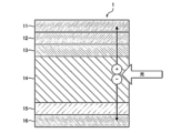
- FIG. 1 is a schematic cross-sectional view showing an example of a layered structure of a photoelectric conversion element according to the present invention.
- the present invention is directed to a photoelectric conversion element, and provides a photoelectric conversion element that can improve the hole transport ability by including a hole transport promotion layer containing a compound having the following specific structure or by including a layer obtained by mixing a hole transport material with the compound.
- the photoelectric conversion element of the present invention is an element that converts light energy into electrical energy or an electrical signal, and includes an imaging element, a photosensor, a solar cell, and the like.
- the photoelectric conversion element of the present invention includes a first electrode, a second electrode, and an organic layer disposed between the first electrode and the second electrode.
- the organic layer includes a hole transport layer and a hole transport promotion layer containing an imide compound represented by the following formula (1) (hereinafter, may be simply referred to as "imide compound (1)”), or includes a layer formed by mixing a hole transport material and imide compound (1).
- the hole transport layer has a role of transporting holes and contains a hole transport material.
- the hole transport promotion layer is disposed between the first electrode and the hole transport layer, has a role of facilitating the exchange of holes between the hole transport layer and the electrode, and contains a hole transport promotion material.
- the imide compound (1) is used as a hole transport promoting material.
- the photoelectric conversion element of the present invention includes a first electrode, a second electrode, and an organic layer and a light receiving layer disposed between the first electrode and the second electrode.
- the element configuration of the photoelectric conversion element will be described below.
- the photoelectric conversion element according to the present invention includes a first electrode, a second electrode, and an organic layer disposed between the first electrode and the second electrode, the organic layer including a hole transport region.
- the hole transport region refers to a region between the first electrode and the light receiving layer, and includes, for example, a hole transport layer and a hole transport promotion layer.
- the imide compound (1) can be used as the hole transport promoting material contained in the hole transport promoting layer (or the hole transport promoting material contained in a layer formed by mixing with the hole transport material).
- the hole transport region is preferably adjacent to the first electrode.
- the photoelectric conversion element may include other layers. Examples of the other layers include layers generally used in photoelectric conversion elements. For example, the other layers include, but are not limited to, a light receiving layer, an electron transport layer, a hole blocking layer, an electron blocking layer, and a buffer layer.
- the photoelectric conversion element according to the present invention has, for example, a first electrode, a hole transport promotion layer, a hole transport layer, and a second electrode laminated in this order, or a first electrode, a layer formed by mixing a hole transport material that forms a hole transport layer with the imide compound (1), and a second electrode laminated in this order.
- the photoelectric conversion element may have, for example, a first electrode, a hole transport promotion layer, and a hole transport layer stacked adjacent to each other in this order, or another layer such as a buffer layer may be interposed between the first electrode and the hole transport promotion layer, or between the hole transport promotion layer and the hole transport layer.
- the photoelectric conversion element of the present invention has a first electrode, a hole transport promotion layer, a hole transport layer, a light receiving layer, and a second electrode stacked in this order.
- the photoelectric conversion element of the present invention has a first electrode, a hole transport promotion layer, a hole transport layer, a light receiving layer, an electron transport layer, and a second electrode stacked in this order.
- the above layers may be stacked adjacent to each other, or other layers may be interposed between any of the above layers.
- the photoelectric conversion element may receive light from either the first electrode side or the second electrode side, and either the first electrode or the second electrode may be a transparent electrode.
- the photoelectric conversion element may have a structure in which a transparent electrode (second electrode), an electron transport layer, a light receiving layer, a hole transport layer, a hole transport promotion layer, and a metal electrode (first electrode) are stacked in this order, or a structure in which a transparent electrode (first electrode), a hole transport promotion layer, a hole transport layer, a light receiving layer, an electron transport layer, and a metal electrode (second electrode) are stacked in this order.
- both the first electrode and the second electrode may be transparent electrodes.
- the organic layer in the photoelectric conversion element of the present invention contains the following imide compound (1).
- Ring A represents an optionally substituted aromatic hydrocarbon ring having 6 to 20 carbon atoms (which may be a monocyclic ring, a condensed ring, or a linked ring containing a plurality of rings);
- Ring B represents an imidazole ring or a fused imidazole ring having 5 to 20 carbon atoms;
- R 1 each independently represents a hydroxyl group, a carboxyl group, a formyl group, an acyl group, a nitro group, a cyano group, a fluorine atom, a chlorine atom, a bromine atom, an iodine atom, a trifluoromethyl group, a methyl group, a fluoroalkyl group having 2 to 10 carbon atoms, a fluoroalkoxy group having 1 to 10 carbon atoms, an alkyl group having 2 to 10 carbon atoms, an aromatic hydrocarbon group having 6 to 20 carbon atoms (which may be a single ring,
- Ar 1 represents an optionally substituted aromatic hydrocarbon group having 6 to 20 carbon atoms (which may be a single ring, a condensed ring, or a linked ring containing multiple rings), or an optionally substituted heteroaromatic hydrocarbon group having 2 to 20 carbon atoms (which may be a single ring, a condensed ring, or a linked ring containing multiple rings).
- Examples of the aromatic hydrocarbon group having 6 to 20 carbon atoms for Ar 1 include a phenyl group, a naphthyl group, an anthryl group, a phenanthrenyl group, a pyrenyl group, a perylenyl group, a triphenylenyl group, a tetracenyl group, a chrysenyl group, a fluorenyl group, a 9,9-dimethylfluorenyl group, a 9,9-diphenylfluorenyl group, a spirobifluorenyl group, a biphenylyl group, a terphenyl group, a naphthylphenyl group, a phenylnaphthyl group, a binaphthyl group, an anthrylphenyl group, and
- heteroaromatic group having 2 to 20 carbon atoms in Ar 1 (which may be a single ring, a condensed ring, or a linked ring containing multiple rings) include a pyridyl group, a pyrimidyl group, a pyrazyl group, a triazyl group, a quinolyl group, an isoquinolyl group, a quinoxalyl group, a quinazolinyl group, a pyridopyrimidinyl group, a benzoquinolyl group, a benzoisoquinolyl group, a phenanthrolyl group, a phenanthridyl group, an acridyl group, a phenazinyl group, a phenoxazinyl group, a phenothiazinyl group, a benzoquinoxalyl group, a hexaazatriphenylenyl group, a thienyl group
- Ar 1 is preferably a phenyl group, a naphthyl group, a pyridyl group, a pyrazyl group, a pyrimidyl group, a triazyl group, a quinolyl group, an isoquinolyl group, a quinoxalyl group, or a quinazolinyl group, and more preferably a phenyl group, a pyridyl group, a pyrazyl group, or a quinolyl group in terms of excellent element characteristics. Furthermore, these groups may be substituted with a substituent described later, and the substituent is more preferably a cyano group.
- R 1 represents a hydroxy group, a carboxyl group, a formyl group, an acyl group, a nitro group, a cyano group, a fluorine atom, a chlorine atom, a bromine atom, an iodine atom, a trifluoromethyl group, a methyl group, a fluoroalkyl group having 2 to 10 carbon atoms, a fluoroalkoxy group having 1 to 10 carbon atoms, an alkyl group having 2 to 10 carbon atoms, an aromatic hydrocarbon group having 6 to 20 carbon atoms (which may be a single ring, a condensed ring, or a linked ring containing multiple rings), a heteroaromatic group having 2 to 20 carbon atoms (which may be a single ring, a condensed ring, or a linked ring containing multiple rings), or a group consisting of a combination of two or more of the above groups or atoms.
- R1 include, but are not limited to, a hydroxyl group, a carboxyl group, a formyl group, an acyl group, a nitro group, a cyano group, a fluorine atom, a chlorine atom, a bromine atom, an iodine atom, a trifluoromethyl group, a perfluoroethyl group, a perfluoropropyl group, a perfluorobutyl group, a perfluoropentyl group, a perfluorohexyl group, a perfluoroheptyl group, a perfluorooctyl group, a methyl group, an ethyl group, a propyl group, a butyl group, a pentyl group, a hexyl group, a heptyl group, an octyl group, a cyclopropyl group, a cyclobutyl
- tricyanophenyl group methylphenyl group, dimethylphenyl group, trimethylphenyl group, fluorophenyl group, difluorophenyl group, trifluorophenyl group, perfluorophenyl group, biphenyl group, pyridylphenyl group, bispyridylphenyl group, trifluoromethylphenyl group, bistrifluoromethylphenyl group, naphthyl group, cyanonaphthyl group, dicyanonaphthyl group, phenylnaphthyl group, pyridylnaphthyl group, anthryl group, phenanthrenyl group, pyrenyl group, perylenyl group, triphenylenyl group, tetracenyl group, chrysenyl group, fluorenyl group, 9,9-dimethylfluorenyl group, 9,9-diphenylfluor
- ring A in formula (1) represents an aromatic hydrocarbon ring having 6 to 20 carbon atoms (which may be a single ring, a condensed ring, or a linked ring containing multiple rings) that may be substituted.
- the aromatic hydrocarbon ring having 6 to 20 carbon atoms (which may be a single ring, a condensed ring, or a linked ring containing multiple rings) include a benzene ring, a naphthalene ring, an anthracene ring, a phenanthrene ring, a pyrene ring, a perylene ring, a triphenylene ring, a tetracene ring, a chrysene ring, a fluorene ring, a 9,9-dimethylfluorene ring, a 9,9-diphenylfluorene ring, a spirobifluorene ring, a biphenyl ring,
- Ring A is preferably a benzene ring, a naphthalene ring, or a perylene ring in terms of ease of synthesis, and is preferably a benzene ring or a naphthalene ring in terms of excellent device performance.
- Ring B in formula (1) represents an imidazole ring or a condensed imidazole ring having 5 to 20 carbon atoms.
- Specific examples of ring B include the following (B-1) to (B-15) as preferred examples.
- Ring B is preferably an imidazole ring (B-1), a benzimidazole ring (B-2), or an imidazopyrazine ring (B-9) in terms of ease of synthesis, and (B-1) is even more preferred in terms of superior device performance.
- the aromatic hydrocarbon ring in ring A, the aromatic hydrocarbon group in Ar 1 and the heteroaromatic group in Ar 1 may have a substituent.
- the substituent here is a hydroxyl group, a carboxyl group, a formyl group, an acyl group, a nitro group, a cyano group, a fluorine atom, a chlorine atom, a bromine atom, an iodine atom, a trifluoromethyl group, a methyl group, a fluoroalkyl group having 2 to 10 carbon atoms, a fluoroalkoxy group having 1 to 10 carbon atoms, an alkyl group having 2 to 10 carbon atoms, an aromatic hydrocarbon group having 6 to 20 carbon atoms (which may be a single ring, a condensed ring, or a linked ring containing multiple rings), a heteroaromatic group having 2 to 20 carbon atoms (which may be a single ring, a condensed ring, or
- substituents include, but are not limited to, a hydroxyl group, a carboxyl group, a formyl group, an acyl group, a nitro group, a cyano group, a fluorine atom, a chlorine atom, a bromine atom, an iodine atom, a phenyl group, a cyanophenyl group, a dicyanophenyl group, a tricyanophenyl group, a fluorophenyl group, a difluorophenyl group, a trifluorophenyl group, a perfluorophenyl group, a biphenyl group, a pyridylphenyl group, a bispyridylphenyl group, a naphthyl group, a cyanonaphthyl group, a dicyanonaphthyl group, a phenylnaphthyl group, a pyri
- phenyl group, naphthyl group, pyridyl group, pyrazyl group, pyrimidyl group, cyano group, cyanophenyl group, dicyanophenyl group, cyanopyridyl group, or dicyanopyridyl group is preferable in terms of excellent element performance, and cyano group is more preferable in terms of ease of synthesis.
- n 0, 1, 2, 3, or 4, provided that when ring B is an imidazole ring, n represents 0, 1, or 2.
- n is preferably 1, 2, 3 or 4, and more preferably 1 or 2 in terms of ease of synthesis.
- imide compound (1) examples include compounds represented by the following formulas (C-1) to (C-416). Among them, compounds represented by (C-1) to (C-140) are more preferred, and compounds represented by (C-2), (C-6), (C-10), (C-52), (C-72) and (C-82) are even more preferred.
- a more preferred embodiment of the imide compound represented by the above formula (1) is a compound represented by the following formula (X-1).
- ring G represents a benzene ring or a naphthalene ring.
- Ring H is selected from the group consisting of the following (H-1), (H-2), and (H-3).
- f is 1 or 2.
- Ar3 represents an aromatic hydrocarbon group having 6 to 20 carbon atoms (which may be a monocyclic ring, a condensed ring, or a linked ring containing multiple rings) which may be substituted with a cyano group, or a heteroaromatic hydrocarbon group having 2 to 20 carbon atoms (which may be a monocyclic ring, a condensed ring, or a linked ring containing multiple rings) which may be substituted with a cyano group.
- the imide compound represented by formula (X-1) has an extended conjugated structure with an expanded conjugated system, and is expected to have a strong interaction with the HOMO orbital of the hole transport material. In addition, it has excellent thermal stability as a deposition material. Therefore, when combined with a hole transport material in a photoelectric conversion element, it is particularly likely to promote hole transport ability.
- Ar 3 is preferably a phenyl group, a pyridyl group, a pyrazyl group or a quinolyl group, and these groups may be substituted with a cyano group.
- Ar3 is one of these groups, the LUMO level can be appropriately adjusted, and the interaction with the adjacent layer can be optimized. Furthermore, the compound is easy to synthesize and has excellent thermal stability as a deposition material.
- Ar 2 in formula (1a) represents an optionally substituted aromatic hydrocarbon group having 6 to 20 carbon atoms (which may be a single ring, a condensed ring, or a linked ring containing multiple rings), or an optionally substituted heteroaromatic group having 2 to 20 carbon atoms (which may be a single ring, a condensed ring, or a linked ring containing multiple rings).
- Specific and preferred examples of Ar 2 include the same as those of ring Ar 1 in formula (1).
- Each R 2 independently represents a hydroxyl group, a carboxyl group, a formyl group, an acyl group, a nitro group, a cyano group, a fluorine atom, a chlorine atom, a bromine atom, an iodine atom, a trifluoromethyl group, a methyl group, a fluoroalkyl group having 2 to 10 carbon atoms, a fluoroalkoxy group having 1 to 10 carbon atoms, an alkyl group having 2 to 10 carbon atoms, an aromatic hydrocarbon group having 6 to 20 carbon atoms (which may be a single ring, a condensed ring, or a linked ring containing multiple rings), an aromatic heteroaromatic group having 2 to 20 carbon atoms (which may be a single ring, a condensed ring, or a linked ring containing multiple rings), or a group in which two or more of the above groups or atoms are combined.
- Ring C represents an optionally substituted aromatic hydrocarbon ring having 6 to 20 carbon atoms (which may be a single ring, a condensed ring, or a linked ring containing a plurality of rings). Specific and preferred examples of ring C include the same as those of ring A in formula (1).
- Ring D represents an imidazole ring or a condensed imidazole ring having 5 to 20 carbon atoms. Specific and preferred examples of ring D include the same as those of ring B in formula (1).
- n 0, 1, 2, 3, or 4; However, when ring C is an imidazole ring, m represents 0, 1 or 2; In terms of excellent device performance, m is preferably 1, 2, 3 or 4, and more preferably 2 in terms of ease of synthesis.
- the aromatic hydrocarbon ring in Ring C, the aromatic hydrocarbon group in Ar2 , and the heteroaromatic group in Ar2 may have a substituent.
- substituent here include the same substituents as those in formula (1).
- Preferred specific examples of compound (1a) include the compounds represented by the formulas (C-1) to (C-392). Among them, the compounds represented by formulas (C-1) to (C-140) are more preferable, and the compounds represented by formulas (C-2), (C-52), (C-72) and (C-82) are even more preferable.
- R3 represents a cyano group, a nitro group, a fluorine atom, a chlorine atom, a bromine atom, an iodine atom, a hydroxy group, a heteroaromatic group having 2 to 20 carbon atoms (which may be a single ring, a condensed ring, or a linked ring containing multiple rings), or an aromatic hydrocarbon group having 6 to 20 carbon atoms (which may be a single ring, a condensed ring, or a linked ring containing multiple rings), or may be a group consisting of a combination of two or more of the above groups or atoms.
- R3 include, but are not limited to, a cyano group, a nitro group, a fluorine atom, a chlorine atom, a bromine atom, an iodine atom, a hydroxyl group, a phenyl group, a cyanophenyl group, a dicyanophenyl group, a tricyanophenyl group, a fluorophenyl group, a difluorophenyl group, a trifluorophenyl group, a perfluorophenyl group, a biphenyl group, a pyridylphenyl group, a bispyridylphenyl group, a naphthyl group, a cyanonaphthyl group, a dicyanonaphthyl group, a phenylnaphthyl group, a pyridylnaphthyl group, an anthryl group, a phenyl
- R 4 , R 5 , R 6 and R 7 each independently represent a hydrogen atom or a cyano group. However, at least two of R 4 , R 5 , R 6 and R 7 are cyano groups.
- p represents 0, 1, or 2. In terms of ease of synthesis, p is preferably 0 or 1, and in terms of excellent device performance, p is more preferably 1.
- q represents 1, 2, 3, 4 or 5; In terms of ease of synthesis, q is preferably 0, 1, or 2, and more preferably 1 in terms of excellent device performance.
- Ar3 represents a heteroaromatic group having 2 to 20 carbon atoms (which may be a single ring, a condensed ring, or a linked ring containing multiple rings), or an aromatic hydrocarbon group having 6 to 20 carbon atoms (which may be a single ring, a condensed ring, or a linked ring containing multiple rings).
- Examples of the aromatic hydrocarbon group having 6 to 20 carbon atoms in Ar3 include a phenyl group, a naphthyl group, an anthryl group, a phenanthrenyl group, a pyrenyl group, a perylenyl group, a triphenylenyl group, a tetracenyl group, a chrysenyl group, a fluorenyl group, a 9,9-dimethylfluorenyl group, a 9,9-diphenylfluorenyl group, a spirobifluorenyl group, a biphenylyl group, a terphenyl group, a naphthylphenyl group, a phenylnaphthyl group, a binaphthyl group, an anthrylphenyl group, a pheny
- X1 represents a nitrogen atom or C- R6
- X2 represents a nitrogen atom or C- R7 , in which R6 and R7 represent the above-mentioned groups.
- Preferred specific examples of compound (1b) include compounds represented by the formulas (C-1) to (C-140) in which n is an even number in C-n (n is 1 to 140), and the formulas (C-323) to (C-392).
- compounds represented by the formulas (C-1) to (C-140) in which n is an even number in C-n (n is 1 to 140) are more preferred, and the compounds represented by (C-52) and (C-82) are even more preferred.
- each R 8 independently represents a cyano group, a nitro group, a fluorine atom, a chlorine atom, a bromine atom, an iodine atom, a hydroxy group, a heteroaromatic group having 2 to 20 carbon atoms (which may be a single ring, a condensed ring, or a linked ring containing multiple rings), or an aromatic hydrocarbon group having 6 to 20 carbon atoms (which may be a single ring, a condensed ring, or a linked ring containing multiple rings), or may be a group consisting of a combination of two or more of the above groups or atoms.
- Specific and preferred examples of R8 include the same as those of R3 in formula (1b).
- Each R 9 independently represents a cyano group, a nitro group, a fluorine atom, a chlorine atom, a bromine atom, an iodine atom, a hydroxyl group, a heteroaromatic group having 2 to 20 carbon atoms (which may be a single ring, a condensed ring, or a linked ring containing multiple rings), or an aromatic hydrocarbon group having 6 to 20 carbon atoms (which may be a single ring, a condensed ring, or a linked ring containing multiple rings), and may be a group consisting of a combination of two or more of the above groups or atoms.
- Specific and preferred examples of R 9 are the same as those of R 4 in formula (1b).
- Ar4 represents a heteroaromatic group having 2 to 20 carbon atoms (which may be a single ring, a condensed ring, or a linked ring containing multiple rings), or an aromatic hydrocarbon group having 6 to 18 carbon atoms (which may be a single ring, a condensed ring, or a linked ring containing multiple rings).
- Specific and preferred examples of Ar 4 include the same as those of Ar 3 in formula (1b).
- Ring E represents an imidazole ring or a condensed imidazole ring having 5 to 20 carbon atoms. Specific and preferred examples of ring E include the same as those of ring B in formula (1).
- r represents 1, 2, 3, or 4. However, when ring E is an imidazole ring, r represents 1 or 2. In terms of excellent device performance, r is preferably 1 or 2, and in terms of ease of synthesis, r is more preferably 2.
- k represents 0, 1, 2, 3, 4 or 5. In terms of ease of synthesis, k is preferably 0, 1, or 2, and more preferably 1 in terms of superior device performance.
- Preferred specific examples of compound (1c) include compounds represented by the above formulas (C-1) to (C-140) in which n is an odd number in C-n (n is 1 to 140), and the above formulas (C-141) to (C-322).
- (C-1), (C-5), (C-9), (C-51), (C-55), (C-59), (C-81), (C-85) and (C-89) are preferred, and the compounds represented by (C-1), (C-51) and (C-81) are even more preferred.
- the imide compound represented by formula (1) can be synthesized by a known method or a combination thereof.
- the imide compound (1) can be synthesized by the method shown in steps 1 to 4 below.
- n, ring A, ring B, R 1 and Ar 1 are defined as above, and ring F represents a vinylene group or a divalent aromatic group having 4 to 19 carbon atoms.
- Step 1 is a method of reacting tetracarboxylic anhydride (2) with amine compound (F-1) to obtain monoimide compound (3).
- the target product can be obtained by following the reaction conditions disclosed in the literature (WO2021/168358A1, Chem. Eur. J. 2006, 12, 6592, J. Phys. Chem. C, 2008, 112, 1721.) or the methods disclosed in Synthesis Reference Examples 1 to 4.
- the amine compound (F-1) used in step 1 can be synthesized, for example, according to the method disclosed in Synlett 2008, 15, 2287. Commercially available products may also be used.
- the equivalent amount of the amine compound (F-1) used in step 1 is preferably in the range of 0.3 to 1.5 equivalents relative to the tetracarboxylic anhydride (2), and more preferably in the range of 0.5 to 1.1 equivalents, in terms of a good yield of the monoimide compound (3).
- Step 1 may be carried out in a solvent.
- the solvent include haloalkanes such as dichloromethane, chloroform, tetrachloromethane, dichloroethane, and tetrachloroethane; ethers such as diisopropyl ether, dibutyl ether, cyclopentyl methyl ether (CPME), tetrahydrofuran (THF), 2-methyltetrahydrofuran, 1,4-dioxane, and dimethoxyethane; aromatic hydrocarbons such as benzene, toluene, xylene, mesitylene, and tetralin; heteroaromatic compounds such as imidazole, pyridine, pyrazine, and quinoline; and aromatic compounds such as ethylene carbonate, propylene carbonate, dimethyl carbonate, diethyl carbonate, ethyl methyl
- esters such as ethyl acetate, butyl acetate, methyl propionate, ethyl propionate, methyl butyrate, and ⁇ -lactone; amides such as N,N-dimethylformamide (DMF), dimethylacetamide (DMAc), and N-methylpyrrolidone (NMP); ureas such as N,N,N',N'-tetramethylurea (TMU) and N,N'-dimethylpropyleneurea (DMPU); sulfoxides such as dimethylsulfoxide (DMSO); alcohols such as methanol, ethanol, isopropyl alcohol, butanol, octanol, benzyl alcohol, ethylene glycol, propylene glycol, diethylene glycol, triethylene glycol, and 2,2,2-trifluoroethanol; and the like. These may be used alone or in any ratio. There is no particular limit to the amount of solvent used. Of these, it is preferable to the amount
- the reaction in step 1 can be accelerated by carrying out the reaction in the presence of a condensing agent.
- the condensing agent include solid acids such as alumina and silica gel; metal chlorides such as titanium tetrachloride, tin tetrachloride, and antimony pentachloride; organic bases such as triethylamine, pyridine, 4-dimethylaminopyridine, diazabicycloundecene, tetramethylethylenediamine, and 1,4-diazabicyclo[2.2.2]octane; and carbodiimides such as 1-[3-(dimethylamino)propyl]-3-ethylcarbodiimide, 1-ethyl-3-(3-dimethylaminopropyl)carbodiimide hydrochloride (EDC), N,N'-dicyclohexylcarbodiimide, N,N'-diisopropylcarbodiimide, N
- Step 1 can be carried out at a temperature appropriately selected from -80°C to 300°C, and is preferably carried out at a temperature appropriately selected from 20°C to 250°C in terms of good reaction yield, and more preferably at a temperature appropriately selected from 50°C to 200°C.
- the monoimide compound (3) can be obtained by carrying out a normal treatment after the completion of step 1. If necessary, it may be purified by appropriately using a general means used by those skilled in the art for purifying organic compounds, such as washing, precipitation, filtration, dialysis, recrystallization, column chromatography, preparative HPLC, or Soxhlet extraction. The monoimide compound (3) may also be subjected to step 2 without purification.
- Step 2 is a method of reacting monoimide compound (3) with diamine compound (F-2) to obtain imide compound (1) (hereinafter, simply referred to as "imide compound (1)") contained in the photoelectric conversion element of the present invention.
- the target product can be obtained by following the reaction conditions disclosed in the literature (WO2021/168358A1, J. Org. Chem. 2009, 74, 8914.) or the methods disclosed in Synthesis Examples C-2, 52, 72 and 82.
- the diamine compound (F-2) used in step 2 can be synthesized, for example, according to the method disclosed in Chem. Eur. J. 2015, 21, 17314. Alternatively, a commercially available product may be used.
- the equivalent amount of the amine compound (F-2) used in step 2 is preferably in the range of 0.5 to 1.5 equivalents relative to the monoimide compound (3), and more preferably in the range of 0.8 to 1.2 equivalents, in terms of a good yield of the imide compound (1).
- Step 2 may be carried out in a solvent.
- the solvent include haloalkanes such as dichloromethane, chloroform, tetrachloromethane, dichloroethane, and tetrachloroethane; ethers such as diisopropyl ether, dibutyl ether, cyclopentyl methyl ether (CPME), tetrahydrofuran (THF), 2-methyltetrahydrofuran, 1,4-dioxane, and dimethoxyethane; aromatic hydrocarbons such as benzene, toluene, xylene, mesitylene, and tetralin; heteroaromatic compounds such as imidazole, pyridine, pyrazine, and quinoline; and aromatic compounds such as ethylene carbonate, propylene carbonate, dimethyl carbonate, diethyl carbonate, ethyl methyl
- esters such as ethyl acetate, butyl acetate, methyl propionate, ethyl propionate, methyl butyrate, and ⁇ -lactone; amides such as N,N-dimethylformamide (DMF), dimethylacetamide (DMAc), and N-methylpyrrolidone (NMP); ureas such as N,N,N',N'-tetramethylurea (TMU) and N,N'-dimethylpropyleneurea (DMPU); sulfoxides such as dimethylsulfoxide (DMSO); alcohols such as methanol, ethanol, isopropyl alcohol, butanol, octanol, benzyl alcohol, ethylene glycol, propylene glycol, diethylene glycol, triethylene glycol, and 2,2,2-trifluoroethanol; and the like. These may be used alone or in any ratio. There is no particular limit to the amount of solvent used. Of these, it is preferable to the amount
- the reaction in step 2 can be promoted by carrying out the reaction in the presence of a condensing agent.
- the condensing agent include solid acids such as alumina and silica gel; metal chlorides such as titanium tetrachloride, tin tetrachloride, and antimony pentachloride; organic bases such as triethylamine, pyridine, 4-dimethylaminopyridine, diazabicycloundecene, tetramethylethylenediamine, and 1,4-diazabicyclo[2.2.2]octane; and carbodiimides such as 1-[3-(dimethylamino)propyl]-3-ethylcarbodiimide, 1-ethyl-3-(3-dimethylaminopropyl)carbodiimide hydrochloride (EDC), N,N'-dicyclohexylcarbodiimide, N,N'-diisopropylcarbodiimide, N,
- Step 2 can be carried out at a temperature appropriately selected from -80°C to 300°C, and is preferably carried out at a temperature appropriately selected from 20°C to 250°C in terms of good reaction yield, and more preferably at a temperature appropriately selected from 50°C to 200°C.
- the imide compound (1) can be obtained by carrying out a normal treatment after completion of step 2. If necessary, it may be purified by any of the general means used by those skilled in the art for purifying organic compounds, such as washing, precipitation, filtration, dialysis, recrystallization, column chromatography, preparative HPLC, or Soxhlet extraction.
- Step 3 is a method of reacting tetracarboxylic anhydride (2) with diamine compound (F-2) to obtain fused ring imidazole compound (4).
- the target product can be obtained by following the reaction conditions disclosed in the literature (WO2021/168358A1, J. Org. Chem. 2009, 74, 8914.) or the methods disclosed in Synthesis Reference Examples 1 to 4.
- the equivalent amount of the diamine compound (F-2) used in step 3 is preferably in the range of 0.5 to 1.5 equivalents relative to the tetracarboxylic anhydride (2), and more preferably in the range of 0.8 to 1.2 equivalents, in terms of a good yield of the fused ring imidazole compound (4).
- Step 3 may be carried out in a solvent.
- the solvent include the same solvents as those exemplified in step 2. These may be used alone or in any mixture ratio.
- the reaction in step 3 can be accelerated by carrying out the reaction in the presence of a condensing agent.
- the condensing agent include the same condensing agents as those exemplified in step 2.
- Organic bases are preferred in terms of their high reaction yield, and triethylamine or pyridine are more preferred in terms of the high purity of the resulting fused ring imidazole compound (4).
- Step 3 can be carried out at a temperature appropriately selected from -80°C to 300°C, and is preferably carried out at a temperature appropriately selected from 20°C to 250°C in terms of good reaction yield, and more preferably at a temperature appropriately selected from 50°C to 200°C.
- Fused ring imidazole compound (4) can be obtained by carrying out a normal treatment after completion of step 3. If necessary, it may be purified using a general means used by those skilled in the art for purifying organic compounds, such as washing, precipitation, filtration, dialysis, recrystallization, column chromatography, preparative HPLC, or Soxhlet extraction. Fused ring imidazole compound (4) may also be subjected to step 4 without purification.
- Step 4 is a method of reacting fused ring imidazole compound (4) with amine compound (F-1) to obtain imide compound (1).
- the target product can be obtained by following the reaction conditions disclosed in the literature (WO2021/168358A1, Chem. Eur. J. 2006, 12, 6592, J. Phys. Chem. C, 2008, 112, 1721.) or the methods disclosed in Synthesis Examples C-2, 52, 72, and 82.
- the equivalent amount of the amine compound (F-1) used in step 4 is preferably in the range of 0.3 to 1.5 equivalents relative to the fused ring imidazole compound (4), and more preferably in the range of 0.5 to 1.0 equivalents, in terms of a good yield of the imide compound (1).
- Step 4 may be carried out in a solvent.
- the solvent include the same solvents as those exemplified in step 1. These may be used alone or in any mixture ratio.
- the reaction in step 4 can be accelerated by carrying out the reaction in the presence of a condensing agent.
- a condensing agent examples include the same condensing agents as those exemplified in step 1.
- Organic bases and condensing agents are preferred in terms of good reaction yield, and triethylamine, pyridine, or EDC are more preferred in terms of good purity of the resulting imide compound (1).
- Step 4 can be carried out at a temperature appropriately selected from -80°C to 300°C, and is preferably carried out at a temperature appropriately selected from 20°C to 250°C in terms of good reaction yield, and more preferably at a temperature appropriately selected from 50°C to 200°C.
- the imide compound (1) can be obtained by carrying out a normal treatment after completion of step 4. If necessary, it may be purified by any of the general means used by those skilled in the art for purifying organic compounds, such as washing, precipitation, filtration, dialysis, recrystallization, column chromatography, preparative HPLC, or Soxhlet extraction.
- the hole transport promoting material of the present invention represented by formula (1a) can be produced using tetracarboxylic acid anhydride (2a), amine compound (F-1a) and diamine compound (F-2a) represented by the following formula according to the reaction conditions disclosed in the literature (WO2021/168358A1, Chem. Eur. J. 2006, 12, 6592, J. Phys. Chem. C, 2008, 112, 1721, J. Org. Chem. 2009, 74, 8914.), the methods disclosed in Synthesis Examples and Reference Examples C-2, 52, 72, 82, and the methods described in steps 1 to 4 above. (In the formula, (1a), (2a), (F-1a) and (F-2a) have the same meanings as above.)
- the imide compound of the present invention represented by formula (1b) (hereinafter, simply referred to as "imide compound (1b)") can be produced by using the tetracarboxylic acid anhydride (2b), amine compound (F-1b) and diamine compound (F-2b) represented by the following formula (WO2021/168358A1, Chem. Eur. J. 2006, 12, 6592, J. Phys. Chem. C, 2008, 112, 1721, J. Org. Chem. 2009, 74, 8914.) according to the reaction conditions disclosed in the synthesis examples and reference examples C-2, 52, 72, 82, and the methods described in steps 1 to 4. (In the formula, (1b), (2b), (F-1b) and (F-2b) have the same meanings as above.)
- the imide compound of the present invention represented by formula (1c) (hereinafter, simply referred to as “imide compound (1c)”) can be produced by using the tetracarboxylic acid anhydride (2c), amine compound (F-1c) and diamine compound (F-2c) represented by the following formula (WO2021/168358A1, Chem. Eur. J. 2006, 12, 6592, J. Phys. Chem. C, 2008, 112, 1721, J. Org. Chem. 2009, 74, 8914.) according to the reaction conditions disclosed in the synthesis examples and reference examples C-2, 52, 72, 82, and the methods described in steps 1 to 4. (In the formula, (1c), (2c), (F-1c) and (F-2c) have the same meanings as above.)
- the imide compound (1) has a so-called "conjugated extended imide structure" having imide rings on the left and right of the aromatic hydrocarbon ring represented by ring A, and an imidazole ring (or a condensed imidazole ring) represented by ring B.
- Such a structure is expected to have a strong interaction with the HOMO orbital of the hole transport material.
- the hole transport promotion layer contains a compound represented by formula (1) or contains a layer formed by mixing a hole transport material and an imide compound (1), thereby enhancing the interaction with the HOMO orbital of the adjacent hole transport layer, and promoting the transfer of carriers between the hole transport layer and the hole transport promotion layer. In this way, since the compound represented by formula (1) has a very deep LUMO level, it is expected that the exchange of holes between the hole transport layer and the electrode will be smooth.
- imide compound (1) can be effectively used as a hole transport promoting material that facilitates the exchange of holes between a hole transport layer and an electrode. They have confirmed that the hole transport ability of a photoelectric conversion element is promoted when imide compound (1) (hole transport promoting material) is combined with a hole transport material. In other words, they have discovered that the energy barrier when carriers generated in the light receiving layer are extracted to the electrode side in a photoelectric conversion element can be reduced by imide compound (1), which is the hole transport promoting material of the present application.
- Examples of the laminate structure of the photoelectric conversion element of the present invention include the following structure (i) or (ii). (i): first electrode/hole transport promotion layer/hole transport layer/light receiving layer/second electrode (ii): first electrode/hole transport promotion layer/hole transport layer/light receiving layer/electron transport layer/second electrode
- FIG. 1 is a schematic cross-sectional view showing an example of the layered configuration of the photoelectric conversion element according to the present invention.
- the photoelectric conversion element according to the first embodiment is an organic imaging element or photosensor having the layered structure shown in FIG.
- the photoelectric conversion element 1 includes a first electrode 11 (first electrode), a hole transport promotion layer 12, a hole transport layer 13, a light receiving layer 14, an electron transport layer 15, and a second electrode 16 (second electrode) in this order.
- first electrode 11 first electrode
- second electrode 16 second electrode
- some of these layers may be omitted, or other layers may be added.
- FIG. 1 shows light incident from the side of the light receiving layer 14.
- a voltage is applied to the photoelectric conversion element 1 so that, of the charges (holes and electrons) generated by photoelectric conversion in the light receiving layer 14, the holes are moved to the first electrode 11 and the electrons are moved to the second electrode 16. That is, the first electrode 11 is used as a hole collecting electrode, and the second electrode 16 is used as an electron collecting electrode.
- the substrate provided on the upper surface of the first electrode 11 is omitted in FIG. 1.
- the substrate here is not particularly limited, and examples include a glass plate, a quartz plate, and a plastic plate.
- the substrate is transparent to the wavelength of light.
- a first electrode 11 or a second electrode 16 is provided on the substrate.
- the first electrode is formed of a transparent material that transmits or substantially transmits the light.
- transmits light means that the average transmittance (of visible light) is 80% or more
- substantially transmits light means that the average transmittance is 50% or more.
- transparent means that the average transmittance is 50% or more.
- the transparent material used for the first electrode 11 or the second electrode 16 is not particularly limited, but examples include indium tin oxide (ITO), indium zinc oxide (IZO), tin oxide, aluminum-doped tin oxide, magnesium indium oxide, nickel tungsten oxide, other metal oxides, metal nitrides such as gallium nitride, metal selenides such as zinc selenide, and metal sulfides such as zinc sulfide.
- ITO indium tin oxide
- IZO indium zinc oxide
- tin oxide aluminum-doped tin oxide
- magnesium indium oxide nickel tungsten oxide
- other metal oxides metal nitrides
- metal selenides such as zinc selenide
- metal sulfides such as zinc sulfide.
- the transmission characteristics of the first electrode 11 are not important. Therefore, examples of materials that can be used for the first electrode in this case include gold, iridium, molybdenum, palladium, platinum, etc.
- a hole transport promoting layer 12 is provided between the first electrode 11 and a hole transport layer 13 described later.
- the hole transport promoting layer 12 is provided to promote hole transport from the hole transport layer 13 to the first electrode 11.
- the hole transport promoting layer 12 contains the above-mentioned imide compound (1).
- a compound other than the imide compound (1) may be contained together. Examples of compounds that may be contained in the hole transport promoting layer 12 include conventionally known hole transport materials, such as the compounds used in the hole transport layer 13 described later.
- the hole transport layer 13 is provided between the hole transport promotion layer 12 and the light receiving layer 14 .
- the hole transport layer 13 has a role of transporting holes generated in the light receiving layer 14 from the light receiving layer 14 to the first electrode 11, and a role of blocking the movement of electrons generated in the light receiving layer 14 toward the first electrode 11.
- the hole transport layer 13 may also have a role of blocking electron injection from the first electrode 11.
- the hole transport layer 13 may be a single layer structure made of one or more materials, or may be a laminate structure made of multiple layers of the same composition or different compositions.
- the hole transport material that can be contained in the hole transport layer 13 may be a known hole transport material. Examples of known hole transport materials include aromatic tertiary amine compounds, naphthalene compounds, anthracene compounds, tetracene compounds, pentacene compounds, phenanthrene compounds, pyrene compounds, perylene compounds, fluorene compounds, carbazole compounds, indole compounds, pyrrole compounds, picene compounds, thiophene compounds, benzotrifuran compounds, benzotrithiophene compounds, naphthodithiophene compounds, naphthothienothiophene compounds, benzodifuran compounds, benzodithiophene compounds, benzothiophene compounds, naphthobisbenzothiophene compounds, chrysenodithioph
- fluorene compounds are preferred, and fluorene compounds, chrysenodithiophene compounds, benzothienobenzothiophene compounds, and indolocarbazole compounds are particularly preferred.
- the light-receiving layer 14 is provided between the hole-transporting layer 13 and the electron-transporting layer 15 described below.
- the light receiving layer 14 can be made of a material having a photoelectric conversion function.
- the light-receiving layer 14 may have a single layer structure made of one or more materials, or may have a laminate structure made of multiple layers of the same composition or different compositions. In particular, in order to increase the photoelectric conversion efficiency, it is preferable that the light receiving layer 14 be made of a layer containing at least two kinds of materials (organic components).
- Examples of materials (organic components) used in the light-receiving layer 14, which has a single-layer structure made of one type of material, include (i) coumarin and its derivatives, quinacridone and its derivatives, and phthalocyanine and its derivatives.
- Examples of materials (organic components) used in the light-receiving layer 14 having a single layer structure made of two kinds of materials include the above-mentioned (i) coumarin and its derivatives, quinacridone and its derivatives, and phthalocyanine and its derivatives, and (ii) fullerene and its derivatives, and other acceptor materials.
- the light-receiving layer 4 made of these materials may be formed by depositing a mixture of powders in advance, or by co-deposition in any ratio.
- materials (organic components) used in the light-receiving layer 14, which has a single-layer structure made of three types of materials include the above-mentioned (i) coumarin and its derivatives, quinacridone and its derivatives, phthalocyanine and its derivatives, (ii) fullerene and its derivatives, other acceptor materials, and (iii) combinations with a hole-transport material.
- the light-receiving layer 14 made of these materials may be formed by depositing a mixture of powders in advance, or by co-deposition in any ratio.
- Specific examples of the coumarin derivative include coumarin 6 and coumarin 30.
- Specific examples of the quinacridone derivative include N,N-dimethylquinacridone.
- Specific examples of the phthalocyanine derivative include boron subphthalocyanine chloride and boron subnaphthalocyanine chloride (SubNC).
- Specific examples of fullerenes and derivatives thereof include [60]fullerene, [70]fullerene, and [6,6]-phenyl-C61-methyl butyrate ([60]PCBM).
- Preferable compounds and specific examples of the hole transport material are the same as those used in the hole transport layer 13 described above.
- the material having the photoelectric conversion function is not limited to being contained only in the light receiving layer.
- the material having the photoelectric conversion function may be contained in a layer adjacent to the light receiving layer 14 (hole transport layer 13 or electron transport layer 15).
- An electron transport layer 15 is provided between the light-receiving layer 14 and a second electrode 16 described below.
- the electron transport layer 15 has a role of transporting electrons generated in the light receiving layer 14 to the second electrode 16, and a role of blocking the movement of holes from the second electrode 16 to the light receiving layer 14.
- the electron transport layer 15 may also have a role of blocking hole injection from the second electrode 16.
- the electron transport material that can be contained in the electron transport layer 15 may be a known electron transport material, and examples of the electron transport material include fullerene, fullerene derivatives, triazine derivatives, bis(8-hydroxyquinolinato)manganese, tris(8-hydroxyquinolinato)aluminum, tris(2-methyl-8-hydroxyquinolinato)aluminum, BCP (2,9-dimethyl-4,7-diphenyl-1,10-phenanthroline), Bp hen (4,7-diphenyl-1,10-phenanthroline), BAlq (bis(2-methyl-8-quinolinolato)-4-(phenylphenolato)aluminum), 4,6-bis(3,5-di(pyridin-4-yl)phenyl)-2-methylpyrimidine, N,N'-diphenyl-1,4,5,8-naphthalenetetracarboxylic acid diimide, and N,N'-di(4-pyridyl)
- the electron transport layer 15 may be a single layer structure made of one or more materials, or a laminate structure made of multiple layers of the same or different compositions.
- a second electrode 16 is provided on the electron transport layer 15 .
- materials for the second electrode 16 include indium-tin oxide (ITO), indium-zinc oxide (IZO), sodium, sodium-potassium alloy, magnesium, lithium, magnesium/copper mixture, magnesium/silver mixture, magnesium/aluminum mixture, magnesium/indium mixture, aluminum/aluminum oxide (Al 2 O 3 ) mixture, indium, lithium/aluminum mixture, gold, platinum, rare earth metal, molybdenum oxide, etc.
- the first electrode 11 and the second electrode 16 may be the same or different.
- Each layer except for the first electrode 11 and the second electrode 16 described above can be formed by forming a thin film of the material of each layer (together with a material such as a binder resin and a solvent, if necessary) by a known method such as a vacuum deposition method, a spin coating method, a casting method, or an LB (Langmuir-Blodgett) method.
- a vacuum deposition method a spin coating method
- a casting method a casting method
- LB Liangmuir-Blodgett
- the first electrode 11 and the second electrode 16 can be formed by forming a thin film of the electrode material by a method such as vapor deposition or sputtering.
- a pattern may be formed through a mask of the desired shape during vapor deposition or sputtering, or a pattern of the desired shape may be formed by photolithography after forming a thin film by vapor deposition or sputtering.
- the film thickness of the first electrode 11 and the second electrode 16 is preferably 1 ⁇ m or less, and more preferably 10 nm or more and 200 nm or less.
- the materials constituting the first electrode 11 and the second electrode 16 may be interchanged as necessary (also called an inverted structure). In this type of structure, light passes through the second electrode 16 and enters the light receiving layer 14, forming a photoelectric conversion element.
- the imaging element equipped with the photoelectric conversion element of this embodiment can be used, for example, as an imaging element in a digital camera or digital video camera, or as an imaging element built into a mobile phone or the like.
- the optical sensor can be used, for example, in a television remote control, an air conditioner switch, or the opening and closing of an automatic door.
- the photoelectric conversion element according to the second embodiment of the present invention is a solar cell having a layered structure shown in Fig. 1.
- a hole transport promotion layer 12 and a hole transport layer 13 are provided between a first electrode 11 and a light receiving layer 14, and an electron transport layer 15 is provided between a second electrode 16 and the light receiving layer 14.
- some of these layers may be omitted, or other layers may be added.
- the first electrode 11 is made of, for example, a transparent material, and the transparent material can be the transparent material in the first embodiment.
- the first electrode 11 may be formed on any substrate (for example, a transparent substrate such as glass, plastic, or polymer film).
- the material of the hole transport promotion layer 12 is the same as the material of the hole transport promotion layer 12 in the first embodiment (imide compound (1)).
- the material of the hole transport promotion layer 12 may contain a conventionally known hole transport material in addition to the material in the first embodiment.
- the material of the hole transport layer 13 is the same as the material of the hole transport layer 13 in the first embodiment.
- the material of the hole transport layer 13 may contain a conventionally known hole transport material in addition to the hole transport material in the first embodiment.
- the material of the light-receiving layer 14 may be any material as long as it contains an electron-donating material and an electron-accepting material, and may be a planar bonding type in which the electron-donating material and the electron-accepting material are bonded to each other on their respective planes, or a bulk heterojunction type in which the electron-donating material and the electron-accepting material are mixed and formed into a film.
- the electron donating material is not particularly limited, but an organic semiconductor is preferred.
- the electron donating material may be, for example, a polymer compound such as a polythiophene derivative, a polyfluorene derivative, or a polyphenylenevinylene derivative, or a copolymer thereof, or a low molecular weight compound such as a phthalocyanine derivative and a metal complex thereof, a porphyrin derivative and a metal complex thereof, an acene derivative such as pentacene, or a diamine derivative.
- the electron donating material may be an inorganic semiconductor together with an organic semiconductor within a range that does not impair the effect of the present invention.
- the electron-accepting material is not particularly limited, but is preferably an organic semiconductor. Examples of the electron-accepting material include fullerene derivatives, perylene derivatives, and naphthalene derivatives.
- the electron transport material in the first embodiment can be used as the material of the electron transport layer 15.
- an alkali metal halide such as sodium fluoride or cesium fluoride, an alkaline earth metal halide such as calcium fluoride, a carbonate such as cesium carbonate, or an inorganic n-type semiconductor such as titanium oxide or zinc oxide may be used.
- the second electrode 16 may be made of, for example, a metal such as magnesium, calcium, sodium, potassium, titanium, indium, yttrium, lithium, gadolinium, aluminum, silver, tin, or lead, or an alloy thereof, but is not limited to these.
- a metal such as magnesium, calcium, sodium, potassium, titanium, indium, yttrium, lithium, gadolinium, aluminum, silver, tin, or lead, or an alloy thereof, but is not limited to these.
- the materials constituting the first electrode 11 and the second electrode 16 may be interchanged as necessary (also called an inverted structure). In this type of structure, light passes through the second electrode 16 and enters the light receiving layer 14, forming a photoelectric conversion element.
- the method for forming each layer is not particularly limited.
- the first electrode 11, the hole transport promotion layer 12, the hole transport layer 13, the light receiving layer 14, the electron transport layer 15, and the second electrode 16 may be laminated in this order on a substrate using a vapor deposition method, a spin coating method, a casting method, a pattern transfer method, or the like; alternatively, after the hole transport promotion layer 12, the hole transport layer 13, the light receiving layer 14, and the electron transport layer 15 are laminated, the first electrode 11 and the second electrode 16 may be formed on this laminate by transfer, vapor deposition, sputtering, or the like, respectively.
- a hole-only device having a structure consisting of a first electrode/a first hole injection layer/a hole transport layer/a hole transport promotion layer/a second electrode was fabricated, and the hole transport properties of the device were evaluated.
- a glass substrate with an ITO transparent electrode having an ITO film (thickness: 110 nm) patterned in a stripe shape was prepared as a substrate having a first electrode on its surface. This substrate was washed with isopropyl alcohol and then subjected to a surface treatment by ozone ultraviolet cleaning.
- the surface on which the ITO film was formed was subjected to vacuum deposition of each layer by a vacuum deposition method, thereby forming each layer in a laminate.
- the glass substrate was placed in a vacuum deposition chamber, and the pressure was reduced to 1.0 ⁇ 10 ⁇ 4 Pa. Then, each layer was prepared according to the film formation conditions in the following order.
- a 1 nm thick MoO3 film was formed on the ITO film to prepare a hole injection layer.
- a hole transport layer was prepared by depositing a film of (HTL-1) to a thickness of 100 nm as a hole transport material. (HTL-1) was synthesized by the method described in JP-A-2018-193371.
- the sublimated and purified compound (A-60) was formed into a film having a thickness of 10 nm to prepare a hole transport promoting layer.
- Example 1 which used compound (C-2) as the hole transport promoting material (HOD voltage: 2.42 V), had a lower HOD voltage than the element of Comparative Example 1, which used the known material NPT (HOD voltage: 6.41 V), and the element of Comparative Example 2, which did not use a hole transport promoting material (HOD voltage: 6.26 V).
- the compounds (C-6), (C-10), (C-52), (C-72), and (C-82) synthesized in Synthesis Examples the effect of improving the transport ability as a hole transport promoting material (reduction in HOD voltage) was observed, similarly to Device Example 1.
- the substrate was then washed with isopropyl alcohol and then subjected to a surface treatment by ozone ultraviolet cleaning.
- Preparation for vacuum deposition After cleaning and surface treatment, each layer was deposited by vacuum deposition on the substrate by vacuum deposition, so that each layer was laminated.
- the glass substrate was placed in a vacuum deposition chamber, and the pressure was reduced to 7.0 ⁇ 10 ⁇ 5 Pa. Then, each layer was prepared according to the film formation conditions in the following order.
- the sublimation-purified compound 4,6-bis(3,5-di(pyridin-4-yl)phenyl)-2-methylpyrimidine was formed into a film having a thickness of 10 nm at a rate of 0.03 nm/sec to prepare an electron transport layer 15 .
- a film of 250 nm was formed by mixing N,N-dimethylquinacridone and fullerene C60 in a ratio of 4:1 (mass ratio) to prepare the light receiving layer 14. The film formation rate was 0.13 nm/sec.
- a hole transport layer 13 was prepared by depositing a hole transport material (HTL-1) at a rate of 0.10 nm/sec to a thickness of 10 nm.
- HTL-1 hole transport material
- C-2 hole transport promotion layer 12
- C-2 hole transport promotion layer 12
- a metal mask was placed perpendicular to the ITO stripes on the substrate, and the first electrode 11 was formed by depositing an Au film to a thickness of 80 nm. The deposition rate of Au was 0.1 nm/sec.
- a photoelectric conversion element 1 having an area of 4 mm 2 as shown in FIG. 1 was prepared.
- a voltage of 2.5 V was applied as an absolute value to the photoelectric conversion element prepared as described above so that electrons were transported to the second electrode 16 side and holes were transported to the first electrode 11 side, the current (dark current) and external quantum efficiency in a dark place were evaluated.
- the dark current (A/cm 2 ) was measured using a Keithley Source Measure Unit 2636B.
- the external quantum efficiency was measured using a solar cell spectral response measuring device (manufactured by Soma Optical Co., Ltd.).
- the wavelength of the irradiated light was 560 nm, and the measurement was performed at an intensity of 50 ⁇ W/cm 2.
- the results are shown in Table 2.
- the external quantum efficiency is a relative value with the result in the element comparative example 3 described later taken as the reference value (100). The lower the value of the dark current, the better the performance, and the higher the value of the external quantum efficiency, the better the performance.
- Comparative Element Example 3 A photoelectric conversion element of Comparative Example 3 was prepared in the same manner as in Example 2, except that the compound (NPT) was used instead of the compound (C-2) in the preparation of the hole transport promotion layer 12, and the dark current and external quantum efficiency were measured in the same manner as in Example 2. The results are shown in Table 2.
- Comparative Element Example 4 A photoelectric conversion element of Comparative Example 4 was prepared in the same manner as in Example 2 except that the hole transport promotion layer 12 was not provided, and the dark current and external quantum efficiency were measured in the same manner as in Example 2. The results are shown in Table 2.
- the photoelectric conversion element of the present invention contains the imide compound (1) above, which can improve the hole transport ability, and when used in a photoelectric conversion element, can perform photoelectric conversion more efficiently.
- the photoelectric conversion element of the present invention contains the imide compound (1) above, which can suppress dark current and increase external quantum efficiency.
Landscapes
- Physics & Mathematics (AREA)
- Chemical & Material Sciences (AREA)
- Electromagnetism (AREA)
- Organic Chemistry (AREA)
- Spectroscopy & Molecular Physics (AREA)
- Engineering & Computer Science (AREA)
- Materials Engineering (AREA)
- Optics & Photonics (AREA)
- Plural Heterocyclic Compounds (AREA)
Priority Applications (1)
| Application Number | Priority Date | Filing Date | Title |
|---|---|---|---|
| JP2025543456A JPWO2025047665A1 (cg-RX-API-DMAC7.html) | 2023-08-30 | 2024-08-26 |
Applications Claiming Priority (2)
| Application Number | Priority Date | Filing Date | Title |
|---|---|---|---|
| JP2023-140235 | 2023-08-30 | ||
| JP2023140235 | 2023-08-30 |
Publications (1)
| Publication Number | Publication Date |
|---|---|
| WO2025047665A1 true WO2025047665A1 (ja) | 2025-03-06 |
Family
ID=94819177
Family Applications (1)
| Application Number | Title | Priority Date | Filing Date |
|---|---|---|---|
| PCT/JP2024/030239 Ceased WO2025047665A1 (ja) | 2023-08-30 | 2024-08-26 | 光電変換素子、正孔輸送促進材料、および化合物 |
Country Status (2)
| Country | Link |
|---|---|
| JP (1) | JPWO2025047665A1 (cg-RX-API-DMAC7.html) |
| WO (1) | WO2025047665A1 (cg-RX-API-DMAC7.html) |
Cited By (1)
| Publication number | Priority date | Publication date | Assignee | Title |
|---|---|---|---|---|
| WO2026116444A1 (ja) * | 2024-11-29 | 2026-06-04 | 三菱瓦斯化学株式会社 | 光電変換素子、撮像素子、光センサー及び固体撮像装置 |
Citations (5)
| Publication number | Priority date | Publication date | Assignee | Title |
|---|---|---|---|---|
| JP2004093791A (ja) * | 2002-08-30 | 2004-03-25 | Canon Inc | ナフタレンアミジンイミド化合物、ナフタレンアミジンイミド化合物を含有する電子写真感光体、該電子写真感光体を有するプロセスカートリッジおよび電子写真装置 |
| JP2004093804A (ja) * | 2002-08-30 | 2004-03-25 | Canon Inc | 電子写真感光体、プロセスカートリッジおよび電子写真装置 |
| JP2014520394A (ja) * | 2011-06-09 | 2014-08-21 | ノヴァレッド・アクチエンゲゼルシャフト | 有機電子素子のための化合物 |
| US20180006243A1 (en) * | 2016-06-30 | 2018-01-04 | Lg Display Co., Ltd. | Organic compound, and organic light emitting diode and organic light emitting display device including the same |
| JP2023107233A (ja) * | 2022-01-21 | 2023-08-02 | 東ソー株式会社 | 光電変換素子 |
-
2024
- 2024-08-26 JP JP2025543456A patent/JPWO2025047665A1/ja active Pending
- 2024-08-26 WO PCT/JP2024/030239 patent/WO2025047665A1/ja not_active Ceased
Patent Citations (5)
| Publication number | Priority date | Publication date | Assignee | Title |
|---|---|---|---|---|
| JP2004093791A (ja) * | 2002-08-30 | 2004-03-25 | Canon Inc | ナフタレンアミジンイミド化合物、ナフタレンアミジンイミド化合物を含有する電子写真感光体、該電子写真感光体を有するプロセスカートリッジおよび電子写真装置 |
| JP2004093804A (ja) * | 2002-08-30 | 2004-03-25 | Canon Inc | 電子写真感光体、プロセスカートリッジおよび電子写真装置 |
| JP2014520394A (ja) * | 2011-06-09 | 2014-08-21 | ノヴァレッド・アクチエンゲゼルシャフト | 有機電子素子のための化合物 |
| US20180006243A1 (en) * | 2016-06-30 | 2018-01-04 | Lg Display Co., Ltd. | Organic compound, and organic light emitting diode and organic light emitting display device including the same |
| JP2023107233A (ja) * | 2022-01-21 | 2023-08-02 | 東ソー株式会社 | 光電変換素子 |
Cited By (1)
| Publication number | Priority date | Publication date | Assignee | Title |
|---|---|---|---|---|
| WO2026116444A1 (ja) * | 2024-11-29 | 2026-06-04 | 三菱瓦斯化学株式会社 | 光電変換素子、撮像素子、光センサー及び固体撮像装置 |
Also Published As
| Publication number | Publication date |
|---|---|
| JPWO2025047665A1 (cg-RX-API-DMAC7.html) | 2025-03-06 |
Similar Documents
| Publication | Publication Date | Title |
|---|---|---|
| KR102475856B1 (ko) | 신규한 화합물 및 이를 이용한 유기발광 소자 | |
| JP7187752B2 (ja) | 新規な化合物およびこれを利用した有機発光素子 | |
| CN112673004A (zh) | 新的化合物和包含其的有机发光器件 | |
| JP2022505594A (ja) | 新規な化合物およびこれを含む有機発光素子 | |
| KR102475855B1 (ko) | 신규한 화합물 및 이를 이용한 유기발광 소자 | |
| TW201837158A (zh) | 有機發光裝置 | |
| JP7785551B2 (ja) | 光電変換素子および撮像素子 | |
| KR102579367B1 (ko) | 신규한 화합물 및 이를 이용한 유기발광 소자 | |
| CN106575708A (zh) | 光电转换元件以及使用其的图像传感器、太阳能电池、单色检测传感器及柔性传感器 | |
| EP4626191A1 (en) | Organic electronic element and compound | |
| WO2024190394A1 (ja) | 有機電子素子、及び化合物 | |
| WO2025134923A1 (ja) | 有機電子素子、イミド化合物及びその製造方法 | |
| TWI646070B (zh) | 具有螺環接結構的化合物及含有其的有機發光裝置 | |
| KR102064413B1 (ko) | 신규한 헤테로 고리 화합물 및 이를 이용한 유기발광 소자 | |
| JP2024117715A (ja) | 光電変換素子、光電変換素子用材料、及び化合物 | |
| KR102341241B1 (ko) | 신규한 화합물 및 이를 이용한 유기발광 소자 | |
| WO2025004567A1 (ja) | 有機電子素子、及び化合物 | |
| JP2023107232A (ja) | 撮像素子用受光素子用材料 | |
| JP2023107233A (ja) | 光電変換素子 | |
| JP7655850B2 (ja) | インデノカルバゾール環を有する化合物からなる有機薄膜を備える光電変換素子 | |
| KR102455462B1 (ko) | 신규한 화합물 및 이를 이용한 유기 발광 소자 | |
| JP7697513B2 (ja) | 正孔輸送促進材料、受光素子用材料、シアノ化合物、および有機受光素子 | |
| WO2025182950A1 (ja) | 有機電子素子、正孔輸送促進材料、及びイミド化合物 | |
| WO2025022986A1 (ja) | 有機電子素子、有機電子素子用材料及びイミド化合物 | |
| WO2026058894A1 (ja) | 有機電子素子、正孔輸送促進材料及びイミド化合物 |
Legal Events
| Date | Code | Title | Description |
|---|---|---|---|
| 121 | Ep: the epo has been informed by wipo that ep was designated in this application |
Ref document number: 24859698 Country of ref document: EP Kind code of ref document: A1 |
|
| ENP | Entry into the national phase |
Ref document number: 2025543456 Country of ref document: JP Kind code of ref document: A |
|
| WWE | Wipo information: entry into national phase |
Ref document number: 2025543456 Country of ref document: JP |
|
| NENP | Non-entry into the national phase |
Ref country code: DE |