WO2025047659A1 - 積層セラミックコンデンサ、積層セラミックコンデンサの製造方法、および、積層セラミックコンデンサの実装構造の製造方法 - Google Patents
積層セラミックコンデンサ、積層セラミックコンデンサの製造方法、および、積層セラミックコンデンサの実装構造の製造方法 Download PDFInfo
- Publication number
- WO2025047659A1 WO2025047659A1 PCT/JP2024/030225 JP2024030225W WO2025047659A1 WO 2025047659 A1 WO2025047659 A1 WO 2025047659A1 JP 2024030225 W JP2024030225 W JP 2024030225W WO 2025047659 A1 WO2025047659 A1 WO 2025047659A1
- Authority
- WO
- WIPO (PCT)
- Prior art keywords
- via conductor
- layer
- electrode layer
- main surface
- external electrode
- Prior art date
- Legal status (The legal status is an assumption and is not a legal conclusion. Google has not performed a legal analysis and makes no representation as to the accuracy of the status listed.)
- Ceased
Links
Images






Classifications
-
- H—ELECTRICITY
- H01—ELECTRIC ELEMENTS
- H01G—CAPACITORS; CAPACITORS, RECTIFIERS, DETECTORS, SWITCHING DEVICES, LIGHT-SENSITIVE OR TEMPERATURE-SENSITIVE DEVICES OF THE ELECTROLYTIC TYPE
- H01G2/00—Details of capacitors not covered by a single one of groups H01G4/00-H01G11/00
- H01G2/02—Mountings
- H01G2/06—Mountings specially adapted for mounting on a printed-circuit support
-
- H—ELECTRICITY
- H01—ELECTRIC ELEMENTS
- H01G—CAPACITORS; CAPACITORS, RECTIFIERS, DETECTORS, SWITCHING DEVICES, LIGHT-SENSITIVE OR TEMPERATURE-SENSITIVE DEVICES OF THE ELECTROLYTIC TYPE
- H01G4/00—Fixed capacitors; Processes of their manufacture
- H01G4/002—Details
- H01G4/228—Terminals
-
- H—ELECTRICITY
- H01—ELECTRIC ELEMENTS
- H01G—CAPACITORS; CAPACITORS, RECTIFIERS, DETECTORS, SWITCHING DEVICES, LIGHT-SENSITIVE OR TEMPERATURE-SENSITIVE DEVICES OF THE ELECTROLYTIC TYPE
- H01G4/00—Fixed capacitors; Processes of their manufacture
- H01G4/30—Stacked capacitors
Definitions
- the present invention relates to a multilayer ceramic capacitor, a method for manufacturing a multilayer ceramic capacitor, and a method for manufacturing a mounting structure for a multilayer ceramic capacitor.
- a multilayer ceramic capacitor is known that has multiple via conductors and multiple external terminals that are electrically connected to the via conductors.
- the multilayer capacitor disclosed in JP-A-7-201651 is characterized in that external electrodes are formed on at least a portion of each of the front and back main surfaces of a laminate consisting of a dielectric and an internal electrode, the internal electrodes and external electrodes of the same polarity are connected to each other by a plurality of columnar connection members, and the columnar connection members (via conductors) are arranged at locations where the magnetic fields caused by the currents flowing through the internal electrodes cancel each other out.
- Patent Document 2 discloses a multilayer capacitor array including a capacitor body, first and second internal electrodes arranged in an alternating manner facing each other with laminated dielectric layers sandwiched therebetween, a first external terminal and a second external terminal formed on at least one of the upper and lower surfaces of the body, and a first conductive via hole and a second conductive via hole formed in the stacking direction of the body and connected to the first external terminal and the second external terminal, respectively.
- the multilayer ceramic capacitors described in Patent Documents 1 and 2 are said to be capable of reducing the equivalent series inductance (ESL). However, there is room for further improvement in reducing the ESL of such multilayer ceramic capacitors.
- the present invention has been made in consideration of the above problems, and aims to provide a multilayer ceramic capacitor, a method for manufacturing a multilayer ceramic capacitor, and a method for manufacturing a mounting structure for a multilayer ceramic capacitor that can further reduce the equivalent series inductance (ESL) of the multilayer ceramic capacitor.
- ESL equivalent series inductance
- a multilayer ceramic capacitor comprises a capacitor body, a first external electrode, and a second external electrode.
- the capacitor body includes a dielectric layer, a plurality of first internal electrode layers and a plurality of second internal electrode layers, a first via conductor, and a second via conductor.
- the plurality of first internal electrode layers and the plurality of second internal electrode layers are alternately stacked in the stacking direction with the dielectric layer sandwiched between them.
- the first via conductor is electrically connected to the plurality of first internal electrode layers.
- the first via conductor extends from the inside of the capacitor body to the first main surface.
- the first main surface is one side of the capacitor body in the stacking direction.
- the second via conductor is electrically connected to the plurality of second internal electrode layers.
- the second via conductor extends from the inside of the capacitor body to the first main surface.
- the first external electrode includes a first base electrode layer and a first surface electrode layer.
- the first base electrode layer is provided on the first main surface so as to cover the first via conductor.
- the first surface electrode layer directly covers the first base electrode layer.
- the second external electrode is disposed on the first principal surface at a distance from the first external electrode and covers the second via conductor. The outer surface of the first surface electrode layer extends away from the edge of the first base electrode layer on the first principal surface.
- a method for manufacturing a multilayer ceramic capacitor according to another aspect of the present invention includes preparing a capacitor body including a dielectric layer, a plurality of first internal electrode layers and a plurality of second internal electrode layers, a first via conductor, and a second via conductor, wherein the plurality of first internal electrode layers and the plurality of second internal electrode layers are alternately stacked in the stacking direction with the dielectric layer in between, the first via conductor is electrically connected to the plurality of first internal electrode layers and extends from the inside of the capacitor body to a first main surface which is one side of the capacitor body in the stacking direction, and the second via conductor is electrically connected to the plurality of second internal electrode layers and extends from the inside of the capacitor body to the first main surface; providing a first external electrode including a first base electrode layer provided on the first main surface so as to cover the first via conductor and a first surface electrode layer directly covering the first base electrode layer; and providing a second external electrode on the first main surface so as to cover the second via conductor at a
- a multilayer ceramic capacitor comprises a capacitor body, a first external electrode, and a second external electrode.
- the capacitor body includes a dielectric layer, a plurality of first internal electrode layers and a plurality of second internal electrode layers, a first via conductor, and a second via conductor.
- the plurality of first internal electrode layers and the plurality of second internal electrode layers are alternately stacked in the stacking direction with the dielectric layer sandwiched between them.
- the first via conductor is electrically connected to the plurality of first internal electrode layers and extends from the inside of the capacitor body to the first main surface.
- the first main surface is one side of the capacitor body in the stacking direction.
- the second via conductor is electrically connected to the plurality of second internal electrode layers.
- the second via conductor extends from the inside of the capacitor body to the first main surface.
- the first external electrode is provided on the first main surface so as to cover the first via conductor.
- the second external electrode is provided on the first main surface so as to cover the second via conductor, spaced apart from the first external electrode.
- the outer surface of the first external electrode extends away from the edge of the first via conductor in the first principal surface.
- a method for manufacturing a multilayer ceramic capacitor according to another aspect of the present invention includes preparing a capacitor body including a dielectric layer, a plurality of first internal electrode layers and a plurality of second internal electrode layers, a first via conductor, and a second via conductor, wherein the plurality of first internal electrode layers and the plurality of second internal electrode layers are alternately stacked in the stacking direction with the dielectric layer in between, the first via conductor is electrically connected to the plurality of first internal electrode layers and extends from the inside of the capacitor body to a first main surface which is one side of the capacitor body in the stacking direction, and the second via conductor is electrically connected to the plurality of second internal electrode layers and extends from the inside of the capacitor body to the first main surface; providing a first external electrode on the first main surface to cover the first via conductor; and providing a second external electrode on the first main surface to cover the second via conductor at a distance from the first external electrode.
- Providing the first external electrode includes forming a first plating layer 30 by
- the present invention makes it possible to further reduce the equivalent series inductance (ESL) of multilayer ceramic capacitors.
- ESL equivalent series inductance
- FIG. 1 is a cross-sectional view showing a multilayer ceramic capacitor according to a first embodiment of the present invention.
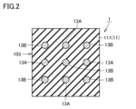
- 2 is a cross-sectional view of the multilayer ceramic capacitor of FIG. 1 as viewed in the direction of the arrows along line II-II.
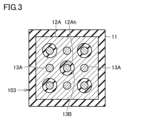
- 3 is a cross-sectional view of the multilayer ceramic capacitor of FIG. 1 as viewed in the direction of the arrows III-III.
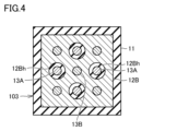
- 4 is a cross-sectional view of the multilayer ceramic capacitor of FIG. 1 as viewed in the direction of the arrows IV-IV.
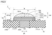
- 2 is a partial cross-sectional view showing a first external electrode and its periphery in the multilayer ceramic capacitor according to the first preferred embodiment of the present invention.
- FIG. 4 is a partial cross-sectional view showing a first external electrode and its periphery of a multilayer ceramic capacitor according to a first modified example.
- FIG. FIG. 11 is a partial cross-sectional view showing a first external electrode and its periphery of a multilayer ceramic capacitor according to a second modified example.
- FIG. 11 is a partial cross-sectional view showing a first external electrode and its periphery of a multilayer ceramic capacitor according to a third modified example.
- FIG. 13 is a partial cross-sectional view showing a first external electrode and its periphery of a multilayer ceramic capacitor according to a fourth modified example.
- FIG. 13 is a cross-sectional view of a multilayer ceramic capacitor according to a fifth modified example, taken along a line passing through a first internal electrode layer.
- FIG. FIG. 13 is a cross-sectional view of a ceramic capacitor according to a fifth modified example, taken along a line passing through a second internal electrode layer.
- 13 is a cross-sectional view of a multilayer ceramic capacitor according to a sixth modified example, taken along a line passing through a first internal electrode layer.
- FIG. FIG. 13 is a cross-sectional view of a ceramic capacitor according to a sixth modified example, taken along a line passing through a second internal electrode layer.
- FIG. 2 is a flow diagram showing a method for manufacturing the multilayer ceramic capacitor according to the first embodiment of the present invention.
- FIG. 2 is a schematic cross-sectional view showing a state immediately after a first plating layer is formed in the method for manufacturing the multilayer ceramic capacitor according to the first embodiment of the present invention.
- FIG. 4 is a cross-sectional SEM image observed immediately after a first plating layer is formed in an experimental example of the production of the ceramic capacitor according to the first embodiment of the present invention. 4 is a cross-sectional SEM photograph showing a state in which a first surface electrode layer is formed in an experimental example of manufacturing the ceramic capacitor according to the first embodiment of the present invention.
- 1 is a schematic cross-sectional view showing a state in which a multilayer ceramic capacitor according to a first embodiment of the present invention and an electronic component are prepared.
- FIG. 1 is a schematic cross-sectional view showing a mounting structure of a multilayer ceramic capacitor according to a first embodiment of the present invention.
- FIG. 4 is a cross-sectional view showing a multilayer ceramic capacitor according to a second embodiment of the present invention.
- FIG. 11 is a cross-sectional view showing a multilayer ceramic capacitor according to a third embodiment of the present invention.
- FIG. 11 is a cross-sectional view showing a multilayer ceramic capacitor according to a fourth embodiment of the present invention.
- FIG. 11 is a partial cross-sectional view showing a first external electrode and its periphery in a multilayer ceramic capacitor according to a fourth embodiment of the present invention.
- FIG. 11 is a flow diagram showing a method for manufacturing a multilayer ceramic capacitor according to a fourth embodiment of the present invention.
- FIG. 11 is a schematic cross-sectional view showing a state immediately after a first plating layer is formed in a manufacturing method of a multilayer ceramic capacitor according to a fourth embodiment of the present invention.
- 11 is a schematic cross-sectional view showing a state in which a multilayer ceramic capacitor according to a fourth embodiment of the present invention and an electronic component are prepared.
- FIG. FIG. 11 is a schematic cross-sectional view showing a mounting structure of a multilayer ceramic capacitor according to a fourth embodiment of the present invention.
- FIG. 1 is a cross-sectional view showing a multilayer ceramic capacitor according to a first embodiment of the present invention.
- Fig. 2 is a cross-sectional view of the multilayer ceramic capacitor of Fig. 1 as viewed in the direction of the arrows II-II.
- Fig. 3 is a cross-sectional view of the multilayer ceramic capacitor of Fig. 1 as viewed in the direction of the arrows III-III.
- Fig. 4 is a cross-sectional view of the multilayer ceramic capacitor of Fig. 1 as viewed in the direction of the arrows IV-IV.
- the multilayer ceramic capacitor 1 comprises a capacitor body 10, a first external electrode 20A, and a second external electrode 20B.
- the capacitor body 10 may have any shape.
- the capacitor body 10 has a rectangular parallelepiped shape as a whole.
- a rectangular parallelepiped shape as a whole means that the shape is not a perfect rectangular parallelepiped shape, for example, a shape in which the corners and edges of the rectangular parallelepiped are rounded, but that has six surfaces and can be considered as a rectangular parallelepiped as a whole.
- the capacitor body 10 has a first main surface 101, a second main surface 102, and a peripheral side surface 103.
- the first main surface 101 is one side of the capacitor body 10 in the stacking direction DS.
- the second main surface 102 is the opposite side of the capacitor body 10 to the first main surface 101.
- the first main surface 101 and the second main surface 102 may have a rectangular outer shape when viewed from the stacking direction DS.
- the peripheral side surface 103 connects the first main surface 101 and the second main surface 102.
- the dimensions of the capacitor body 10 are arbitrary, but for example, when viewed from the first main surface 101 side, the vertical dimension of the rectangle can be 0.3 mm or more and 3.0 mm or less, the horizontal dimension can be 0.3 mm or more and 3.0 mm or less, and the dimension in the stacking direction DS can be 50 ⁇ m or more and 200 ⁇ m or less.
- the capacitor body 10 includes a plurality of dielectric layers 11, a plurality of first internal electrode layers 12A, a plurality of second internal electrode layers 12B, a plurality of first via conductors 13A, and a plurality of second via conductors 13B.
- the multiple dielectric layers 11 include a first outer layer portion 111 and a second outer layer portion 112.
- the first outer layer portion 111 is the dielectric layer 11 located closest to the first main surface 101 among the multiple dielectric layers 11.
- the first outer layer portion 111 forms a part of the first main surface 101.
- the second outer layer portion 112 is the dielectric layer 11 located closest to the second main surface 102 among the multiple dielectric layers 11.
- the second outer layer portion 112 forms the entire second main surface 102.
- the peripheral side surface 103 is entirely formed of multiple dielectric layers 11 including the first outer layer portion 111 and the second outer layer portion 112.
- the dielectric layer 11 may be made of any material, and may be made of, for example, a ceramic material mainly composed of BaTiO3 , CaTiO3 , SrTiO3 , SrZrO3 , or CaZrO3 .
- These main components may contain a minor component selected from the group consisting of Mn compounds, Fe compounds, Cr compounds, Co compounds, and Ni compounds, the minor component being contained in a smaller amount than the main component.
- the multiple first internal electrode layers 12A and multiple second internal electrode layers 12B are alternately stacked one layer at a time in the stacking direction DS with the dielectric layer 11 in between.
- the first internal electrode layers 12A and the second internal electrode layers 12B face each other via the dielectric layer 11, thereby forming a capacitance.
- the multilayer ceramic capacitor 1 becomes a multilayer ceramic capacitor with a high capacitance density in which multiple capacitor functional parts are densely arranged side by side.
- each of the multiple second internal electrode layers 12B is integrally formed within the same layer (see FIG. 4).
- the second internal electrode layer 12B has a rectangular outer shape that is approximately the same as the first internal electrode layer 12A when viewed from the stacking direction DS.
- a multiple number of second through holes 12Bh are formed in each of the multiple second internal electrode layers 12B to allow a multiple number of first via conductors 13A, which will be described later, to pass through.
- the material of the first internal electrode layer 12A and the second internal electrode layer 12B is arbitrary, and may contain, for example, a metal such as Ni, Cu, Ag, Pd, Pt, Fe, Ti, Cr, Sn, or Au, or an alloy containing these metals, as a main component.
- the first internal electrode layer 12A and the second internal electrode layer 12B may contain, as a common material, the same ceramic material as the dielectric ceramic contained in the dielectric layer 11. In that case, the proportion of the common material contained in the first internal electrode layer 12A and the second internal electrode layer 12B is, for example, 20 vol % or less.
- each of the first internal electrode layer 12A and the second internal electrode layer 12B is arbitrary, but can be, for example, about 0.3 ⁇ m or more and 1.0 ⁇ m or less.
- the number of layers of the first internal electrode layer 12A and the second internal electrode layer 12B is arbitrary, but can be, for example, about 10 layers or more and 150 layers or less in total.
- Each of the multiple first via conductors 13A is electrically connected to at least one of the multiple first internal electrode layers 12A. In this embodiment, each of the multiple first via conductors 13A is electrically connected to each of the multiple first internal electrode layers 12A.
- the multiple first via conductors 13A extend from the inside of the capacitor body 10 to the first main surface 101.
- the multiple first via conductors 13A extend along the stacking direction DS.
- the first via conductors 13A are not exposed from the second main surface 102.
- the multiple first via conductors 13A pass through second through holes 12Bh formed in each of the multiple second internal electrode layers 12B. Therefore, the multiple first via conductors 13A are insulated from the multiple second internal electrode layers 12B.
- Each of the multiple second via conductors 13B is electrically connected to at least one of the multiple second internal electrode layers 12B. In this embodiment, each of the multiple second via conductors 13B is electrically connected to each of the multiple second internal electrode layers 12B.
- the multiple second via conductors 13B extend from the inside of the capacitor body 10 to the first main surface 101.
- the multiple second via conductors 13B extend along the stacking direction DS.
- the second via conductors 13B are not exposed from the second main surface 102.
- the multiple second via conductors 13B pass through second through holes 12Bh formed in each of the multiple first internal electrode layers 12A. Therefore, the multiple second via conductors 13B are insulated from the multiple first internal electrode layers 12A.
- the shape of the multiple first via conductors 13A and second via conductors 13B is arbitrary, and can be, for example, cylindrical.
- the diameter of the first via conductors 13A and second via conductors 13B is, for example, about 20 ⁇ m or more and 150 ⁇ m or less.
- the distance between adjacent first via conductors 13A and second via conductors 13B, more specifically, the distance between the center of the first via conductor 13A and the center of the second via conductor 13B is, for example, about 50 ⁇ m or more and 500 ⁇ m or less.
- the material of the first via conductor 13A and the second via conductor 13B is arbitrary, and may be, for example, a metal such as Ni, Cu, Ag, Pd, Pt, Fe, Ti, Cr, Sn, or Au, or an alloy containing these metals.
- the material of the first via conductor 13A and the second via conductor 13B is preferably, for example, Ni or an alloy containing Ni.
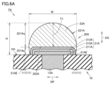
- FIG. 5 is a partial cross-sectional view showing a first external electrode and its periphery of the multilayer ceramic capacitor according to embodiment 1 of the present invention.
- the multiple first external electrodes 20A are provided on the first main surface 101 so as to cover the corresponding first via conductors 13A. More specifically, the multiple first external electrodes 20A each cover the edge of the corresponding first via conductor 13A and the dielectric layer 11 (first outer layer portion 111) on the first main surface 101.
- Each of the multiple first external electrodes 20A includes a first base electrode layer 21A and a first surface electrode layer 22A.
- the first base electrode layer 21A is provided on the first principal surface 101 so as to cover the corresponding first via conductor 13A. Specifically, the first base electrode layer 21A covers the boundary between the corresponding first via conductor 13A and the dielectric layer 11 (first outer layer portion 111) on the first principal surface 101.
- the specific internal configuration of the first base electrode layer 21A is not particularly limited.
- the first base electrode layer 21A includes a baked electrode layer 211A and a first base plating layer 212A and a second base plating layer 213A as base plating layers.
- the baked electrode layer 211A is provided on the first principal surface 101 so as to directly cover the first via conductor 13A. Specifically, the baked electrode layer 211A covers the boundary between the corresponding first via conductor 13A and the dielectric layer 11 (first outer layer portion 111) on the first principal surface 101.
- the baked electrode layer 211A preferably contains the same type of metal as the metal contained in the first via conductor 13A.
- the material of the baked electrode layer 211A is preferably Ni or an alloy containing Ni.
- a ceramic material is further added to the baked electrode layer 211A as a co-material to improve the bonding strength with the dielectric layer 11.
- the undercoat plating layer covers the entire surface of the baked electrode layer 211A that is not in contact with the first main surface 101.
- the first undercoat plating layer 212A directly covers the entire surface of the baked electrode layer 211A that is not in contact with the first main surface 101.
- the second undercoat plating layer 213A is coated on the side opposite the baked electrode layer 211A from the first undercoat plating layer 212A.
- Materials constituting the undercoat plating layer include Cu, Ni, and Au.
- the first undercoat plating layer 212A contains Cu
- the second undercoat plating layer 213A contains Ni.
- the shape of the first base electrode layer 21A when viewed from the stacking direction DS is not particularly limited.
- the shape of the first base electrode layer 21A when viewed from the stacking direction DS may be circular, for example. If the shape of the first base electrode layer 21A when viewed from the stacking direction DS is circular, the shapes of the baked electrode layer 211A, the first base plating layer 212A, and the second base plating layer 213A when viewed from the stacking direction DS are each circular.
- the thickness of each of the baked electrode layer 211A, the first base plating layer 212A, and the second base plating layer 213A is, for example, 1 ⁇ m or more and 10 ⁇ m or less.
- the first surface electrode layer 22A directly covers the first base electrode layer 21A.
- the first surface electrode layer 22A covers the entire portion of the first base electrode layer 21A that is not in contact with the first main surface 101.
- the outer surface 221A of the first surface electrode layer 22A extends from the edge 21AE of the first base electrode layer 21A on the first principal surface 101 away from the first principal surface 101.
- the outer surface 221A of the first surface electrode layer 22A includes a first region 221Ap and a second region 221Aq in the stacking direction DS.
- the first region 221Ap is in contact with the edge 21AE.
- the second region 221Aq is located on the opposite side of the first main surface 101 from the first region 221Ap.
- the first region 221Ap extends such that the cross-sectional area of the first external electrode 20A when viewed from the stacking direction DS increases with increasing distance from the first main surface 101.
- the second region 221Aq extends such that the cross-sectional area of the first external electrode 20A when viewed from the stacking direction DS decreases with increasing distance from the first main surface 101.
- the outer surface 221A of the first surface electrode layer 22A extends in a generally curved shape.
- the shape of the first base electrode layer 21A is circular when viewed from the stacking direction DS, the outer surface 221A of the first surface electrode layer 22A extends in a generally spherical shape.
- the thickness T1 in the stacking direction DS of the central portion of the first surface electrode layer 22A in the planar direction DP parallel to the first main surface 101 is greater than the average thickness of the first surface electrode layer 22A, which is the average thickness from the inner surface 222A, which is the surface of the first surface electrode layer 22A that contacts the first base electrode layer 21A, to the outer surface 221A.
- the central portion of the first surface electrode layer 22A in the planar direction DP is the center portion (center of gravity portion) when the first surface electrode layer 22A is viewed from the stacking direction DS.
- the thickness from the inner surface 222A to the outer surface 221A when viewed from an arbitrary point on the inner surface 222A is the thickness of the first surface electrode layer 22A on the normal line when a normal line is virtually drawn to the inner surface 222A at that point.
- the average thickness from the inner surface 222A to the outer surface 221A can be calculated by, for example, averaging the above thicknesses when viewed from five different points on the inner surface 222A.
- the height dimension H of the first surface electrode layer 22A in the stacking direction DS from the first main surface 101 is, for example, about 10 ⁇ m or more and 20 ⁇ m or less.
- the larger the height dimension H of the first surface electrode layer 22A the larger the distance between the capacitor body 10 and the electronic component can be when the first surface electrode layer 22A is reflow soldered to the electronic component. Therefore, by setting the height dimension H to 10 ⁇ m or more, the underfill resin for filling the gap between the capacitor body 10 and the electronic component can be easily injected into the gap.
- the height dimension H of the first surface electrode layer 22A is not limited to the above range.
- the width dimension W which is the maximum dimension of the first surface electrode layer 22A in the plane direction DP, is appropriately set to correspond to the dimension of the first via conductor 13A in the plane direction DP.
- the width dimension W is the diameter dimension of the first surface electrode layer 22A when viewed from the stacking direction DS.
- the width dimension W of the first surface electrode layer 22A is, for example, 120 ⁇ m or less, preferably 100 ⁇ m or less, and more preferably 75 ⁇ m or less.
- the smaller the width dimension W of the first surface electrode layer 22A the smaller the center distance between the first external electrode 20A and the second external electrode 20B described later can be designed in the plane direction DP.
- the width dimension W of the first surface electrode layer 22A may be, for example, 30 ⁇ m or more, or 50 ⁇ m or more.
- the ratio (W/H), which is the value obtained by dividing the width dimension W by the height dimension H of the first surface electrode layer 22A, is preferably, for example, 3.0 or less, and more preferably 1.5 or less.
- the first surface electrode layer 22A is preferably formed from a material having a melting point lower than the melting point of the material constituting the first base electrode layer 21A. This makes it easy to maintain the shape of the first base electrode layer 21A when the first surface electrode layer 22A is reflow soldered to an electronic component. It also makes it easy to form the first surface electrode layer 22A into the above-mentioned shape (details will be described later).
- the first surface electrode layer 22A is preferably formed from an alloy containing a metal such as Sn or Sn and Ag.
- the second external electrodes 20B are spaced apart from the first external electrodes 20A.
- the second external electrodes 20B are arranged on the first main surface 101 so as to cover the corresponding second via conductors 13B. More specifically, the second external electrodes 20B each cover the boundary between the corresponding second via conductor 13B and the dielectric layer 11 (first outer layer portion 111) on the first main surface 101.
- the second external electrode 20B when viewed from the corresponding second via conductor 13B can have the same configuration as the first external electrode 20A when viewed from the corresponding first via conductor 13A.
- Each of the multiple second external electrodes 20B includes a second base electrode layer 21B and a second surface electrode layer 22B.
- the second base electrode layer 21B is provided on the first main surface 101 so as to cover the corresponding second via conductor 13B. Specifically, the second base electrode layer 21B covers the boundary between the corresponding second via conductor 13B and the dielectric layer 11 (first outer layer portion 111) on the first main surface 101.
- the second base electrode layer 21B in the second external electrode 20B can have a configuration similar to the configuration that the first base electrode layer 21A in the first external electrode 20A can have.
- the second base electrode layer 21B has a baked electrode layer, a first base plating layer, and a second base plating layer similar to those of the first base electrode layer 21A (not shown).
- the second surface electrode layer 22B directly covers the second base electrode layer 21B.
- the second surface electrode layer 22B covers the entire portion of the second base electrode layer 21B that is not in contact with the first main surface 101.
- the outer surface 221B of the second surface electrode layer 22B extends from the edge 21BE of the second base electrode layer 21B on the first main surface 101 away from the first main surface 101. Furthermore, the second surface electrode layer 22B when viewed from the corresponding second base electrode layer 21B and second via conductor 13B can have a similar configuration to the first surface electrode layer 22A when viewed from the corresponding first base electrode layer 21A and first via conductor 13A.
- the height dimension H of the first surface electrode layer 22A (and the second surface electrode layer 22B) can have various values.
- the first base electrode layer 21A (and the second base electrode layer 21B) can have various layer structures.
- multilayer ceramic capacitors according to each modified example of this embodiment will be described. In the description of each modified example, the same configuration as in embodiment 1 will not be repeated.
- FIG. 6A is a partial cross-sectional view showing the first external electrode and its surroundings of the multilayer ceramic capacitor according to the first modified example.
- the multilayer ceramic capacitor 1w according to the first modified example of embodiment 1 of the present invention has a larger height dimension H than the first surface electrode layer 22A (see FIG. 5) in this embodiment.
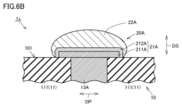
- FIG. 6B is a partial cross-sectional view showing the first external electrode and its periphery of the multilayer ceramic capacitor according to the second modified example.
- the base plating layer in the first base electrode layer 21A is composed only of the first base plating layer 212A.
- the first surface electrode layer 22A directly covers the first base plating layer 212A.
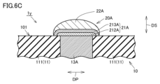
- FIG. 6C is a partial cross-sectional view showing the first external electrode and its periphery of the multilayer ceramic capacitor according to the third modified example.
- the first base electrode layer 21A does not include a fired electrode layer.
- the first base electrode layer 21A includes only the first base plating layer 212A and the second base plating layer 213A.
- the first base plating layer 212A is provided on the first main surface 101 so as to directly cover the first via conductor 13A.
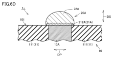
- FIG. 6D is a partial cross-sectional view showing the first external electrode and its periphery of the multilayer ceramic capacitor according to the fourth modified example.
- the first base electrode layer 21A consists only of the first base plating layer 212A. Therefore, in this modified example, the first base plating layer 212A is provided on the first main surface 101 so as to directly cover the first via conductor 13A, and the first surface electrode layer 22A directly covers the first base plating layer 212A.
- first via conductors 13A and the second via conductors 13B are arranged alternately in both one direction and a direction perpendicular to the one direction when viewed from the stacking direction DS (see Figures 3 and 4), but the arrangement of the first via conductors 13A and the second via conductors 13B when viewed from the stacking direction DS is not limited to the above arrangement.
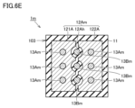
- FIG. 6E is a cross-sectional view of a multilayer ceramic capacitor according to the fifth modified example, taken along a section passing through the first internal electrode layer.
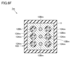
- FIG. 6F is a cross-sectional view of a multilayer ceramic capacitor according to the fifth modified example, taken along a section passing through the second internal electrode layer.
- the first via conductors 13Am are adjacent to each other in one direction
- the second via conductors 13Bm are adjacent to each other.
- the first internal electrode layer 12Am includes a plurality of first internal electrode portions 121A, 122A that are spaced apart from each other in the same layer.
- only one second internal electrode layer 12Bm is located in the same layer, but the second internal electrode layer 12Bm may also include a plurality of second internal electrode layers that are spaced apart from each other in the same layer.
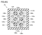
- FIG. 6G is a cross-sectional view of a multilayer ceramic capacitor according to a sixth modified example, taken along a section passing through the first internal electrode layer.
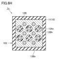
- FIG. 6H is a cross-sectional view of a multilayer ceramic capacitor according to a sixth modified example, taken along a section passing through the second internal electrode layer.
- the direction in which the first via conductors 13An and the second via conductors 13Bn are arranged intersects with one side of the peripheral side surface 103 that extends in a rectangular shape.
- Fig. 7 is a flow diagram showing the method for manufacturing the multilayer ceramic capacitor according to the first embodiment of the present invention.
- the method for manufacturing the multilayer ceramic capacitor according to the first embodiment of the present invention includes a step S1 of preparing a capacitor body, a step S2 of providing a first external electrode, and a step S3 of providing a second external electrode.
- the capacitor body 10 shown in FIG. 1 is prepared.
- the specific method of preparing the capacitor body 10 is not particularly limited.
- a laminate is formed by stacking a plurality of ceramic green sheets corresponding to the plurality of dielectric layers 11 and a conductive paste layer corresponding to the plurality of first internal electrode layers 12A and the plurality of second internal electrode layers 12B on each other in a predetermined pattern.
- a plurality of through holes penetrating the laminate in the lamination direction are formed by laser irradiation. Then, the plurality of through holes are filled with conductive paste.
- a plurality of columnar conductive pastes corresponding to the plurality of first via conductors 13A and the plurality of second via conductors 13B of the capacitor body 10 are provided in the laminate.
- an outer layer ceramic green sheet corresponding to at least a part of the second outer layer portion 112 is further laminated on the laminate so as to cover one side of the columnar conductive pastes.
- the plurality of columnar conductive pastes are not exposed on one side (the surface corresponding to the second main surface 102) of the laminate.
- the laminate having the multiple columnar conductive pastes and the outer ceramic green sheets is fired. This forms the capacitor body 10.
- step S2 of providing a first external electrode the first external electrode 20A shown in Figs. 1 and 5 is provided on the first main surface 101 of the capacitor body 10.
- step S2 of providing a first external electrode includes step S21 of forming a first base electrode layer, step S22 of forming a first plating layer, step S23 of heating and melting the first plating layer, and step S24 of cooling the first plating layer to form a first surface electrode layer.
- the first undercoat plating layer 212A is formed by plating the baked electrode layer 211A.
- the second undercoat plating layer 213A is formed by plating the first undercoat plating layer 212A.
- These plating processes may be, for example, plating processes using a rotary plating method.
- the first undercoat plating layer 212A is formed by plating the first via conductor 13A. In this case, during the plating process, the first undercoat plating layer 212A also grows in the planar direction DP. Therefore, the first undercoat plating layer 212A is provided so as to cover the boundary between the dielectric layer 11 (first outer layer portion 111) and the first via conductor 13A.
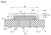
- FIG. 8 is a schematic cross-sectional view showing the state immediately after the first plating layer is formed in the manufacturing method of the multilayer ceramic capacitor according to the first embodiment of the present invention.
- the first plating layer 30A is formed by plating on the first base electrode layer 21A.
- the first plating layer 30A is formed by plating the first base electrode layer 21A.
- the first plating layer 30A is formed so as to cover the entire portion of the first base electrode layer 21A that is not in contact with the first main surface 101.
- the outer surface 301A which is the surface of the first plating layer 30A exposed to the outside, is located away from the edge 21AE of the first base electrode layer 21A on the first main surface 101.
- the thickness Tp1 in the stacking direction DS of the central portion of the first plating layer 30A in the surface direction DP is approximately equal to the average thickness of the first plating layer 30A, which is the average from the inner surface 302A, which is the surface of the first plating layer 30A that is in contact with the first base electrode layer 21A, to the outer surface 301A.
- step S23 of heating and melting the first plating layer the first plating layer 30A formed as described above is heated and melted.
- the melted first plating layer 30A is deformed into a curved shape due to its surface tension so that the area of the outer surface 301A approaches the minimum area in the volume of the first plating layer 30A, more specifically, into a substantially spherical shape. Due to this deformation, the thickness Tp1 at the center portion of the first plating layer 30A increases, and the height dimension Hp in the stacking direction DS of the first plating layer 30A also increases. On the other hand, due to this deformation, the width dimension Wp, which is the maximum dimension in the planar direction DP of the first plating layer 30A, decreases.
- the bonding strength between the first plating layer 30A and the first outer layer portion 111 is relatively low, and the bonding strength between the first plating layer 30A and the first base electrode layer 21A is relatively high.
- the outer surface 301A of the first plating layer 30A deforms so as to extend from the edge 21AE of the first base electrode layer 21A on the first main surface 101 toward the first main surface 101.
- step S24 of forming the first surface electrode layer by cooling the first plating layer the first plating layer 30A that has been melted and deformed as described above is cooled and solidified.
- FIG. 9 is a cross-sectional SEM image of the state immediately after the first plating layer is formed in an experimental example of the manufacture of the multilayer ceramic capacitor according to embodiment 1 of the present invention.
- FIG. 10 is a cross-sectional SEM photograph of the state after the first surface electrode layer is formed in an experimental example of the manufacture of the multilayer ceramic capacitor according to embodiment 1 of the present invention.
- reference numerals corresponding to the reference numerals used in the description of the multilayer ceramic capacitor 1 according to embodiment 1 of the present invention are used.
- the width dimension W of the first surface electrode layer 22A is smaller than the width dimension Wp of the first plating layer 30A before heating and melting.
- the height dimension H of the first surface electrode layer 22A is larger than the height dimension Hp of the first plating layer 30A before heating and melting.
- the thickness T1 of the central portion of the first surface electrode layer 22A is thicker than the thickness Tp1 of the central portion of the first plating layer 30A before heating and melting.
- the ratio (W/H) of the first surface electrode layer 22A is smaller than the ratio (Wp/Hp) which is the value obtained by dividing the width dimension Wp by the height dimension Hp of the first plating layer 30A before heating and melting.
- the heating and cooling conditions in steps S33 and S34 can be adjusted appropriately depending on the material of the first plating layer 30A (first surface electrode layer 22A).
- the heating and cooling conditions can be the same as the solder reflow conditions according to IPC/J-STD.
- the peak temperature in step S33 is, for example, 260°C.
- step S3 of providing a second external electrode the second external electrode 20B shown in FIG. 1 is provided on the first main surface 101 of the capacitor body 10.
- step S3 of providing a second external electrode includes step S31 of forming a second base electrode layer, step S32 of forming a second plating layer, step S33 of heating and melting the second plating layer, and step S34 of cooling the second plating layer to form a second surface electrode layer.
- the step S3 of providing the second external electrode may be performed simultaneously with the step S2 of providing the first external electrode.
- the step S31 of forming the second base electrode layer is performed simultaneously with the step S21 of forming the first base electrode layer.
- the step S32 of forming the second plating layer is performed simultaneously with the step S22 of forming the first plating layer.
- the step S33 of heating and melting the second plating layer is performed simultaneously with the step S23 of heating and melting the first plating layer.
- the step S34 of cooling the second plating layer to form the second surface electrode layer is performed simultaneously with the step S24 of cooling the first plating layer to form the first surface electrode layer.
- step S31 of forming the second base electrode layer the second base electrode layer 21B shown in FIG. 1 and FIG. 5 is provided on the main surface of the capacitor body 10.
- the method of forming the second base electrode layer 21B when viewed from the corresponding second via conductor 13B can be the same as the method of forming the first base electrode layer 21A when viewed from the first via conductor 13A.
- the second plating layer can be formed on the second base electrode layer 21B by the same method as the method of forming the first plating layer 30A on the first base electrode layer 21A.
- the heating conditions in step S33 of heating and melting the second plating layer may be the same as the heating conditions in step S23 of heating and melting the first plating layer. This causes the second plating layer to deform in the same way as the first plating layer 30A.
- the conditions for cooling the heated and melted second plating layer in step S34 of cooling the second plating layer to form the second surface electrode layer 22B may be the same as the cooling conditions in step S24 of cooling the first plating layer to form the first surface electrode layer 22A.
- the multilayer ceramic capacitor 1 according to embodiment 1 of the present invention is manufactured by the above-described manufacturing method. Note that the manufacturing method of the multilayer ceramic capacitor 1 according to embodiment 1 of the present invention is not limited to the above-described manufacturing method.
- FIG. 11 is a schematic cross-sectional view showing a state in which the multilayer ceramic capacitor according to the first embodiment of the present invention and an electronic component are prepared.
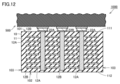
- Fig. 12 is a schematic cross-sectional view showing the mounting structure of the multilayer ceramic capacitor according to the first embodiment of the present invention.
- the method for manufacturing a mounting structure for a multilayer ceramic capacitor includes a step of preparing a multilayer ceramic capacitor 1 manufactured by the above-mentioned manufacturing method, and a step of electrically connecting the multiple first surface electrode layers 22A of the multilayer ceramic capacitor 1 to the electronic component 500 by reflow soldering the multiple first surface electrode layers 22A to the electronic component 500. In this way, a mounting structure 1000 for a multilayer ceramic capacitor is manufactured.
- the manufacturing method for the mounting structure of the multilayer ceramic capacitor in this embodiment further includes a step of electrically connecting the second surface electrode layers 22B to the electronic component 500 by reflow soldering the second surface electrode layers 22B to the electronic component 500. This step can be performed simultaneously with the step of reflow soldering the first surface electrode layer 22A.
- the multiple first surface electrode layers 22A and multiple second surface electrode layers 22B manufactured by the manufacturing method of the multilayer ceramic capacitor in this embodiment are formed so that the thickness of the central portion in the planar direction DP is relatively large. This makes it easy to reflow solder the multiple first surface electrode layers 22A and multiple second surface electrode layers 22B. Therefore, the multilayer ceramic capacitor 1 can be easily mounted on the electronic component 500, and the mounting structure 1000 of the multilayer ceramic capacitor can be more easily manufactured.
- the multilayer ceramic capacitor 1 includes a capacitor body 10, a first external electrode 20A, and a second external electrode 20B.
- the capacitor body 10 includes a dielectric layer 11, a plurality of first internal electrode layers 12A and a plurality of second internal electrode layers 12B, a first via conductor 13A, and a second via conductor 13B.
- the plurality of first internal electrode layers 12A and the plurality of second internal electrode layers 12B are alternately stacked in the stacking direction DS with the dielectric layer 11 in between.
- the first via conductor 13A is electrically connected to the plurality of first internal electrode layers 12A.
- the first via conductor 13A extends from the inside of the capacitor body 10 to the first main surface 101.
- the first main surface 101 is one side of the capacitor body 10 in the stacking direction DS.
- the second via conductor 13B is electrically connected to the plurality of second internal electrode layers 12B.
- the second via conductor 13B extends from the inside of the capacitor body 10 to the first main surface 101.
- the first external electrode 20A includes a first base electrode layer 21A and a first surface electrode layer 22A.
- the first base electrode layer 21A is provided on the first main surface 101 so as to cover the first via conductor 13A.
- the first surface electrode layer 22A directly covers the first base electrode layer 21A.
- the second external electrode 20B is provided on the first main surface 101 so as to cover the second via conductor 13B with a gap between it and the first external electrode 20A.
- the outer surface 221A of the first surface electrode layer 22A extends away from the edge 21AE of the first base electrode layer 21A on the first main surface 101 toward the first main surface 101.
- the thickness in the planar direction DP perpendicular to the stacking direction DS of the first surface electrode layer 22A is relatively small near the edge 21AE of the first base electrode layer 21A. Therefore, the center distance between the first external electrode 20A and the second external electrode 20B in the planar direction DP can be designed to be small, and thus the distance between the first via conductor 13A and the second via conductor 13B can be reduced. If the distance between the first via conductor 13A and the second via conductor 13B can be reduced, the magnetic field induced by the current flowing through the first via conductor 13A and the magnetic field induced by the current flowing through the second via conductor 13B are more likely to cancel each other out.
- the above configuration makes it possible to reduce the equivalent series inductance (ESL) of the multilayer ceramic capacitor 1.
- the thickness T1 in the stacking direction DS of the central portion of the first surface electrode layer 22A in the planar direction DP parallel to the first main surface 101 is greater than the average thickness of the first surface electrode layer 22A, which is the average thickness from the inner surface 222A, which is the surface of the first surface electrode layer 22A that contacts the first base electrode layer 21A, to the outer surface 221A.
- the thickness T1 of the first surface electrode layer 22A in the stacking direction DS is relatively large.
- the distance between the capacitor body 10 and the electronic component 500 can be relatively large when the first surface electrode layer 22A is reflow soldered to the electronic component 500. Therefore, underfill resin for filling the gap between the capacitor body 10 and the electronic component 500 can be easily provided in the gap.
- the outer surface 221A of the first surface electrode layer 22A includes a first region 221Ap and a second region 221Aq in the stacking direction DS.
- the first region 221Ap is in contact with the edge 21AE.
- the second region 221Aq is located on the opposite side of the first main surface 101 from the first region 221Ap.
- the first region 221Ap extends such that the cross-sectional area of the first external electrode 20A when viewed from the stacking direction DS increases with increasing distance from the first main surface 101.
- the second region 221Aq extends such that the cross-sectional area of the first external electrode 20A when viewed from the stacking direction DS decreases with increasing distance from the first main surface 101.
- the above configuration prevents the thickness from the inner surface 222A to the outer surface 221A of the first surface electrode layer 22A in the first region 221Ap from becoming too small, ensuring the strength of the first surface electrode layer 22A. Furthermore, in the second region 221Aq, the dimension of the first surface electrode layer 22A in the planar direction DP can be reduced. This allows the center distance between the first external electrode 20A and the second external electrode 20B in the planar direction DP to be further reduced. As a result, the distance between the first via conductor 13A and the second via conductor 13B can be further reduced, and the equivalent series inductance (ESL) of the multilayer ceramic capacitor 1 can be further reduced.
- ESL equivalent series inductance
- first via conductor 13A and the second via conductor 13B are not exposed from the second main surface 102, which is the surface opposite the first main surface 101 of the capacitor body 10.
- the above configuration makes it possible to prevent short circuits between the multilayer ceramic capacitor 1 and other electronic components arranged on the second main surface 102 side of the multilayer ceramic capacitor 1.
- the method for manufacturing a multilayer ceramic capacitor according to embodiment 1 of the present invention includes a capacitor body 10 including a dielectric layer 11, a plurality of first internal electrode layers 12A and a plurality of second internal electrode layers 12B, a first via conductor 13A, and a second via conductor 13B, in which the plurality of first internal electrode layers 12A and the plurality of second internal electrode layers 12B are alternately stacked in a stacking direction DS with the dielectric layer 11 in between, the first via conductor 13A is electrically connected to the plurality of first internal electrode layers 12A, and a first via conductor 13A is electrically connected to the plurality of first internal electrode layers 12A from the inside of the capacitor body 10, which is a surface on one side of the capacitor body 10 in the stacking direction DS.
- the method includes preparing a capacitor body 10, in which a first via conductor 13A extends to the first main surface 101, and a second via conductor 13B is electrically connected to a plurality of second internal electrode layers 12B and extends from the inside of the capacitor body 10 to the first main surface 101; providing a first external electrode 20A including a first base electrode layer 21A provided on the first main surface 101 so as to cover the first via conductor 13A and a first surface electrode layer 22A directly covering the first base electrode layer 21A; and providing a second external electrode 20B on the first main surface 101 at a distance from the first external electrode 20A so as to cover the second via conductor 13B.
- Providing the first external electrode 20A includes forming a first base electrode layer 21A, forming a first plating layer 30A on the first base electrode layer 21A by plating, heating and melting the first plating layer 30A, and cooling the heated and melted first plating layer 30A to form a first surface electrode layer 22A.
- the outer surface of the first plating layer 30A is deformed into a substantially spherical shape.
- the dimension of the first surface electrode layer 22A in the planar direction DP becomes smaller than the dimension of the first plating layer 30A in the planar direction DP. Therefore, the center distance between the first external electrode 20A and the second external electrode 20B in the planar direction DP can be designed to be small, and thus the distance between the first via conductor 13A and the second via conductor 13B can be reduced.
- the magnetic field induced by the current flowing through the first via conductor 13A and the magnetic field induced by the current flowing through the second via conductor 13B are more likely to cancel each other out.
- the above configuration makes it possible to reduce the equivalent series inductance (ESL) of the multilayer ceramic capacitor 1.
- the thickness T1 at the center of the first surface electrode layer 22A becomes greater than the thickness Tp1 at the center of the first plating layer 30A.
- the manufacturing method for the mounting structure of the multilayer ceramic capacitor according to the first embodiment of the present invention includes preparing a multilayer ceramic capacitor 1 manufactured by the above-mentioned manufacturing method, and electrically connecting the first surface electrode layer 22A of the multilayer ceramic capacitor 1 to the electronic component 500 by reflow soldering the first surface electrode layer 22A to the electronic component 500.
- the above configuration makes it easy to provide underfill resin in the gap between the capacitor body 10 and the electronic component 500 to fill the gap.
- the multilayer ceramic capacitor according to the second embodiment of the present invention differs from the multilayer ceramic capacitor 1 according to the first embodiment of the present invention in that it further includes a third external electrode and a fourth external electrode. Therefore, description of the same configuration and effects as those of the multilayer ceramic capacitor according to the first embodiment of the present invention will not be repeated.
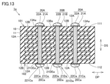
- FIG. 13 is a cross-sectional view showing a multilayer ceramic capacitor according to embodiment 2 of the present invention.
- the multilayer ceramic capacitor 1a further includes a third external electrode 20Ca and a fourth external electrode 20Da.
- the first via conductor 13Aa extends from the inside of the capacitor body 10 to the second principal surface 102.
- the second via conductor 13Ba extends from the inside of the capacitor body 10 to the second principal surface 102.
- the third external electrode 20Ca includes a third base electrode layer 21Ca and a third surface electrode layer 22Ca.
- the third base electrode layer 21Ca is provided on the second principal surface 102 so as to cover either the first via conductor 13Aa or the second via conductor 13Ba.
- the third surface electrode layer 22Ca directly covers the third base electrode layer 21Ca.
- the fourth external electrode 20Da is spaced apart from the third external electrode 20Ca and is provided on the second principal surface 102 so as to cover the other of the first via conductor 13Aa and the second via conductor 13Ba.
- the outer surface 221Ca of the third surface electrode layer 22Ca extends away from the edge 21CEa of the third base electrode layer 21Ca on the second principal surface 102 toward the second principal surface 102.
- the center distance between the third external electrode 20Ca and the fourth external electrode 20Da in the planar direction DP can be designed to be small, and thus the distance between the first via conductor 13Aa and the second via conductor 13Ba can be reduced to reduce the equivalent series inductance (ESL) of the multilayer ceramic capacitor 1a.
- the multilayer ceramic capacitor 1a specifically includes a plurality of third external electrodes 20Ca and a plurality of fourth external electrodes 20Da.
- the third external electrodes 20Ca are provided on the second principal surface 102 so as to cover the respective first via conductors 13Aa.
- the third base electrode layer 21Ca is provided on the second principal surface 102 so as to cover the corresponding first via conductors 13Aa.
- the third external electrode 20Ca when viewed from the second principal surface 102 may have the same configuration as the first external electrode 20A when viewed from the first principal surface 101.
- the multiple fourth external electrodes 20Da are provided on the second principal surface 102 so as to cover the multiple second via conductors 13Ba.
- the fourth external electrode 20Da includes a fourth base electrode layer 21Da and a fourth surface electrode layer 22Da.
- the fourth base electrode layer 21Da is provided on the second principal surface 102 so as to cover the second via conductors 13Ba.
- the fourth surface electrode layer 22Da directly covers the fourth base electrode layer 21Da.
- the outer surface 221Da of the fourth surface electrode layer 22Da also extends away from the edge 21DEa of the fourth base electrode layer 21Da on the second principal surface 102 toward the second principal surface 102.
- the fourth external electrode 20Da when viewed from the second principal surface 102 may have a configuration similar to that of the second external electrode 20B when viewed from the first principal surface 101.
- the method for manufacturing the multilayer ceramic capacitor according to this embodiment further includes a step of providing the third external electrode 20Ca and a step of providing the fourth external electrode 20Da.
- the step of providing the third external electrode 20Ca may have the same configuration as the step S2 of providing the first external electrode 20A when viewed from above the first main surface 101.
- the step of providing the third external electrode 20Ca may be performed simultaneously in parallel with the step S2 of providing the first external electrode 20A.
- the step of providing the fourth external electrode 20Da may have the same configuration as the step S3 of providing the second external electrode 20B when viewed from above the first main surface 101.
- the step of providing the fourth external electrode 20Da may be performed simultaneously in parallel with the step S3 of providing the second external electrode 20B.
- the process of providing the third external electrode 20Ca and the process of providing the fourth external electrode 20Da can be carried out, for example, by clamping the capacitor body 10 with a jig so that the components for the third external electrode 20Ca and the fourth external electrode 20Da are not grounded.
- the outer layer ceramic green sheets are not stacked on the laminate so that both sides of the columnar conductive paste in the stacking direction DS are not covered by the outer layer portion.
- the multilayer ceramic capacitor according to the third embodiment of the present invention has a different shape of the third surface electrode layer and the fourth surface electrode layer from the multilayer ceramic capacitor according to the second embodiment of the present invention. Therefore, the description of the same configuration and effects as those of the multilayer ceramic capacitor according to the second embodiment of the present invention will not be repeated.
- FIG. 14 is a cross-sectional view showing a multilayer ceramic capacitor according to embodiment 3 of the present invention.
- the thickness T3 in the stacking direction DS of the central portion of third surface electrode layer 22Cb in the planar direction DP parallel to first main surface 101 is smaller than the thickness T1 in the stacking direction DS of the central portion of first surface electrode layer 22A in the planar direction DP parallel to first main surface 101.
- the overall dimension of multilayer ceramic capacitor 1b in the stacking direction DS can be made relatively small.
- the thickness T4 in the stacking direction DS of the central portion of the fourth surface electrode layer 22Db in the planar direction DP is smaller than the thickness T1 in the stacking direction DS of the central portion of the first surface electrode layer 22A in the planar direction DP parallel to the first principal surface 101.
- the plating layers in the process of heating and melting the plating layers provided on the respective base electrode layers to form the third surface electrode layer 22Cb and the fourth surface electrode layer 22Db, the plating layers can be heated and melted while the orientation of the capacitor body 10 is fixed so that the second main surface 102 of the capacitor body 10 faces upward in the vertical direction. This causes the heated and melted plating layers to be deformed as if crushed by their own weight, and the third surface electrode layer 22Cb and the fourth surface electrode layer 22Db having a relatively small thickness in the central portion can be formed.
- the third surface electrode layer 22Cb and the fourth surface electrode layer 22Db having a relatively small thickness in the central portion can be formed by sucking up a part of the heated and melted plating layer.
- the multilayer ceramic capacitor according to the fourth embodiment of the present invention differs from the multilayer ceramic capacitor 1 according to the first embodiment of the present invention in the configurations of the first external electrodes and the second external electrodes.
- the same configurations and effects as those of the multilayer ceramic capacitor 1 according to the first embodiment of the present invention and a method for manufacturing the same, as well as the method for manufacturing a mounting structure of the multilayer ceramic capacitor will not be described repeatedly.
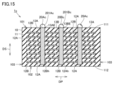
- FIG. 15 is a cross-sectional view showing a multilayer ceramic capacitor according to embodiment 4 of the present invention.
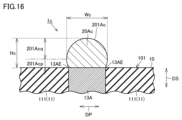
- Fig. 16 is a partial cross-sectional view showing a first external electrode and its periphery of the multilayer ceramic capacitor according to embodiment 4 of the present invention.
- the outer surface 201Ac of the first external electrode 20Ac extends away from the edge 13AE of the first via conductor 13A on the first principal surface 101 toward the first principal surface 101.
- the dimension of the first external electrode 20Ac in the planar direction DP can be reduced near the edge 13AE of the first via conductor 13A. Therefore, the center distance between the first external electrode 20Ac and the second external electrode 20Bc in the planar direction DP can be designed to be small, and thus the distance between the first via conductor 13A and the second via conductor 13B can be reduced. If the distance between the first via conductor 13A and the second via conductor 13B can be reduced, the magnetic field induced by the current flowing through the first via conductor 13A and the magnetic field induced by the current flowing through the second via conductor 13B are more likely to cancel each other out.
- the above configuration makes it possible to reduce the equivalent series inductance (ESL) of the multilayer ceramic capacitor 1c.
- the outer surface 201Ac of the first external electrode 20Ac includes a first region 201Acp and a second region 201Acq in the stacking direction DS.
- the first region 201Acp is in contact with the edge 13AE.
- the second region 201Acq is located on the opposite side of the first main surface 101 from the first region 201Acp.
- the first region 201Acp extends such that the cross-sectional area of the first external electrode 20Ac when viewed from the stacking direction DS increases with increasing distance from the first main surface 101.
- the second region 201Acq extends such that the cross-sectional area of the first external electrode 20Ac when viewed from the stacking direction DS decreases with increasing distance from the first main surface 101.
- the above configuration prevents the dimension of the first external electrode 20Ac in the planar direction DP from becoming too small in the first region 201Acp, and ensures the strength of the first external electrode 20Ac. Also, in the second region 201Acq, the dimension of the first external electrode 20Ac in the planar direction DP can be reduced. This makes it possible to further reduce the center distance between the first external electrode 20Ac and the second external electrode 20Bc in the planar direction DP. As a result, the distance between the first via conductor 13A and the second via conductor 13B can be further reduced, and the equivalent series inductance (ESL) of the multilayer ceramic capacitor 1c can be further reduced.
- ESL equivalent series inductance
- the first external electrode 20Ac and the second external electrode 20Bc in embodiment 4 of the present invention will be described in detail below.
- the outer surface 201Ac of the first external electrode 20Ac is, more specifically, expanded in a substantially curved shape, and even more specifically, expanded in a substantially spherical shape.
- the height dimension Hc of the first external electrode 20Ac in the stacking direction DS is, for example, about 10 ⁇ m or more and 20 ⁇ m or less.
- the upper limit of the height dimension Hc of the first external electrode 20Ac is not particularly limited. However, the height dimension Hc of the first external electrode 20Ac is not limited to the above range.
- the width dimension Wc which is the maximum dimension of the first external electrode 20Ac in the planar direction DP, is appropriately set to correspond to the dimension of the first via conductor 13A in the planar direction DP.
- the width dimension Wc is, for example, 120 ⁇ m or less, preferably 100 ⁇ m or less, and more preferably 75 ⁇ m or less.
- There is no particular lower limit set for the width dimension Wc of the first external electrode 20Ac but the width dimension Wc may be, for example, 30 ⁇ m or more, or 50 ⁇ m or more.
- the ratio (Wc/Hc), which is the value obtained by dividing the width dimension Wc by the height dimension Hc of the first external electrode 20Ac, is preferably, for example, 3.0 or less, and more preferably 1.5 or less.
- Each of the multiple first external electrodes 20Ac is made of a single member.
- the multiple first external electrodes 20Ac are preferably formed of a material having a melting point lower than the melting point of the material that constitutes the first via conductor 13A. This makes it easier to form the first surface electrode layer 22A into the shape described above (details will be described later).
- the first external electrodes 20Ac are preferably formed of an alloy containing, for example, Sn or a metal such as Sn and Ag.
- the outer surface 201Bc of the second external electrode 20Bc extends away from the edge 13BE of the corresponding second via conductor 13B on the first principal surface 101 toward the first principal surface 101. In this way, the second external electrode 20Bc when viewed from the corresponding second via conductor 13B can have the same configuration as the first external electrode 20Ac when viewed from the corresponding first via conductor 13A.
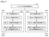
- FIG. 17 is a flow diagram showing the method for manufacturing the multilayer ceramic capacitor according to the fourth embodiment of the present invention.
- Fig. 18 is a schematic cross-sectional view showing a state immediately after the first plating layer is formed in the method for manufacturing the multilayer ceramic capacitor according to the fourth embodiment of the present invention.
- providing a first external electrode 20Ac includes forming a first plating layer 30Ac by plating on the first via conductor 13A on the first main surface 101 (S22c), heating and melting the first plating layer 30Ac (S23c), and cooling the heated and melted first plating layer 30Ac to form a first external electrode 20Ac (S24c).
- the outer surface of the first plating layer 30Ac is deformed into a substantially spherical shape by heating and melting the first plating layer 30Ac.
- the first plating layer 30Ac deformed by heating and melting is cooled to form the first external electrode 20Ac, so that the width dimension Wc of the first external electrode 20Ac becomes smaller than the width dimension Wpc, which is the maximum dimension of the first plating layer 30Ac in the planar direction DP. Therefore, the center distance between the first external electrode 20Ac and the second external electrode 20Bc in the planar direction DP can be designed to be small, and thus the distance between the first via conductor 13A and the second via conductor 13B can be reduced.
- the magnetic field induced by the current flowing through the first via conductor 13A and the magnetic field induced by the current flowing through the second via conductor 13B are more likely to cancel each other out.
- the distance between the first via conductor 13A and the second via conductor 13B can be reduced, and the equivalent series inductance (ESL) of the multilayer ceramic capacitor 1c can be reduced.
- the height dimension Hc of the first external electrode 20Ac becomes larger than the height dimension Hpc of the first plating layer 30A.
- the step S2c of providing a first external electrode includes a step S22c of forming a first plating layer, a step S23c of heating and melting the first plating layer, and a step S24c of cooling the first plating layer to form the first external electrode.
- the first via conductor 13A is plated to form the first plating layer 30Ac.
- This plating may be, for example, a plating process using a rotation plating method.
- the first plating layer 30Ac also grows in the planar direction DP during the plating process. Therefore, the first plating layer 30Ac is provided so as to cover the boundary between the dielectric layer 11 (first outer layer portion 111) and the first via conductor 13A.
- step S23c of heating and melting the first plating layer the first plating layer 30Ac formed as described above is heated and melted.
- the surface tension of the melted first plating layer 30Ac causes the area of the outer surface 301Ac to deform into a curved shape so as to approach the minimum area in the volume of the first plating layer 30Ac, specifically, to deform into an approximately spherical shape.
- This deformation increases the height dimension Hpc of the first plating layer 30Ac.
- this deformation reduces the width dimension Wpc of the first plating layer 30Ac.
- the bonding strength between the first plating layer 30Ac and the first outer layer portion 111 is relatively low, and the bonding strength between the first plating layer 30Ac and the first via conductor 13A is relatively high.
- the outer surface 301Ac of the first plating layer 30Ac deforms so as to extend from the edge 13AE of the first via conductor 13A on the first main surface 101 toward the first main surface 101.
- step S24c of forming the first external electrode by cooling the first plating layer the first plating layer 30Ac that has been melted and deformed as described above is cooled and solidified.
- the width dimension Wc of the first external electrode 20Ac is smaller than the width dimension Wpc of the first plating layer 30Ac before heating and melting.
- the height dimension Hc of the first external electrode 20Ac is larger than the height dimension Hpc of the first plating layer 30Ac before heating and melting.
- the ratio (Wc/Hc) of the first external electrode 20Ac is smaller than the ratio (Wpc/Hpc) of the first plating layer 30A before heating and melting.
- the step S3c of providing the second external electrode includes a step S32c of forming a second plating layer, a step S33c of heating and melting the second plating layer, and a step S34c of cooling the second plating layer to form the second external electrode.
- the step S32c of forming the second plating layer is performed simultaneously with the step S22c of forming the first plating layer.
- the step S33c of heating and melting the second plating layer is performed simultaneously with the step S23c of heating and melting the first plating layer.
- the step S34c of cooling the second plating layer to form the second surface electrode layer is performed simultaneously with the step S24c of cooling the first plating layer to form the first surface electrode layer.
- the method of forming the second external electrode 20Bc when viewed from the corresponding second via conductor 13B can be the same as the method of forming the first external electrode 20Ac when viewed from the first via conductor 13A.
- the second plating layer in the step S32c of forming the second plating layer, can be formed on the second via conductor 13B by the same method as the method of forming the first plating layer 30A on the first via conductor 13A.
- the heating conditions in the step S33c of heating and melting the second plating layer may be the same as the heating conditions in the step S23c of heating and melting the first plating layer.
- the second plating layer is also deformed in the same way as the first plating layer 30Ac.
- the conditions for cooling the heated and melted second plating layer in the step S34c of cooling the second plating layer to form the second external electrode 20Bc may be the same as the cooling conditions in the step S24 of cooling the first plating layer to form the first external electrode 20Ac.
- the multilayer ceramic capacitor 1c according to the fourth embodiment of the present invention is manufactured by the above-described manufacturing method. Note that the manufacturing method of the multilayer ceramic capacitor 1c according to the fourth embodiment of the present invention is not limited to the above-described manufacturing method.
- FIG. 19 is a schematic cross-sectional view showing a state in which the multilayer ceramic capacitor according to the fourth embodiment of the present invention and an electronic component are prepared.
- Fig. 20 is a schematic cross-sectional view showing a mounting structure of the multilayer ceramic capacitor according to the fourth embodiment of the present invention.
- the method for manufacturing a mounting structure of a multilayer ceramic capacitor according to embodiment 4 of the present invention includes a step of preparing a multilayer ceramic capacitor 1c manufactured by the above-mentioned method for manufacturing a multilayer ceramic capacitor, and a step of electrically connecting the first external electrode 20Ac of the multilayer ceramic capacitor 1c to the electronic component 500 by reflow soldering the first external electrode 20Ac to the electronic component 500.
- the above configuration produces a multilayer ceramic capacitor mounting structure 1000c.
- the above configuration also makes it easy to provide an underfill resin in the gap between the capacitor body 10 and the electronic component 500.
- the manufacturing method for the mounting structure of the multilayer ceramic capacitor in this embodiment further includes a step of electrically connecting the second external electrode 20Bc to the electronic component 500 by reflow soldering the second external electrode 20Bc to the electronic component 500. This step can be performed simultaneously with the step of reflow soldering the first external electrode 20Ac.
- the capacitor body includes: A dielectric layer; a plurality of first internal electrode layers and a plurality of second internal electrode layers alternately stacked in a stacking direction with the dielectric layer interposed therebetween; a first via conductor electrically connected to the plurality of first internal electrode layers and extending from inside the capacitor body to a first main surface which is a surface on one side of the capacitor body in the stacking direction; a second via conductor electrically connected to the plurality of second internal electrode layers and extending from the inside of the capacitor body to the first main surface,
- the first external electrode is a first base electrode layer provided on the first principal surface so as to cover the first via conductor; a first surface electrode layer directly covering the first base electrode layer; the second external electrode is provided on the first main surface at a distance from the first external electrode to cover the second via conductor; a first surface electrode layer extending from an edge of the first base electrode layer on the first principal surface so as to be away from the first principal surface;
- ⁇ 2> 2 The multilayer ceramic capacitor according to claim 1, wherein a thickness in the stacking direction of a central portion of the first surface electrode layer in a plane direction parallel to the first main surface is greater than an average thickness of the first surface electrode layer, which is an average of a thickness from an inner surface, which is a surface of the first surface electrode layer in contact with the first base electrode layer, to the outer surface.
- the outer surface of the first surface electrode layer includes, in the stacking direction, a first region in contact with the edge and a second region located on an opposite side of the first main surface from the first region; the first region extends such that a cross-sectional area of the first external electrode when viewed in the stacking direction increases with increasing distance from the first main surface,
- ⁇ 4> The multilayer ceramic capacitor according to any one of ⁇ 1> to ⁇ 3>, wherein the first via conductor and the second via conductor are not exposed from a second main surface of the capacitor body, which is an opposite surface to the first main surface.
- a third external electrode; a fourth external electrode; the first via conductor extends from inside the capacitor body to a second main surface of the capacitor body that is an opposite surface to the first main surface, the second via conductor extends from an interior of the capacitor body to the second principal surface,
- the third external electrode is a third base electrode layer provided on the second principal surface so as to cover either the first via conductor or the second via conductor; a third surface electrode layer directly covering the third base electrode layer; the fourth external electrode is provided on the second main surface at a distance from the third external electrode to cover the other of the first via conductor and the second via conductor;
- the multilayer ceramic capacitor according to any one of ⁇ 1> to ⁇ 4>, wherein an outer surface of the third surface electrode layer extends from an edge of the third base electrode layer on the second main surface so as to be away from the second main surface.
- ⁇ 6> The multilayer ceramic capacitor according to ⁇ 5>, wherein a thickness in the stacking direction of a central portion of the third surface electrode layer in a surface direction parallel to the first main surface is smaller than a thickness in the stacking direction of a central portion of the first surface electrode layer in a surface direction parallel to the first main surface.
- a capacitor body including a dielectric layer, a plurality of first internal electrode layers and a plurality of second internal electrode layers, a first via conductor, and a second via conductor, wherein the plurality of first internal electrode layers and the plurality of second internal electrode layers are alternately stacked in a stacking direction with the dielectric layer sandwiched therebetween, the first via conductor is electrically connected to the plurality of first internal electrode layers and extends from inside the capacitor body to a first main surface which is one surface of the capacitor body in the stacking direction, and the second via conductor is electrically connected to the plurality of second internal electrode layers and extends from inside the capacitor body to the first main surface; providing a first external electrode including a first base electrode layer provided on the first main surface so as to cover the first via conductor and a first surface electrode layer directly covering the first base electrode layer; providing a second external electrode on the first main surface at a distance from the first external electrode so as to cover the second via conductor, Providing the first external electrode includes: forming
- ⁇ 8> Preparing a multilayer ceramic capacitor manufactured by the method for manufacturing a multilayer ceramic capacitor according to ⁇ 7>; and electrically connecting the first surface electrode layer of the multilayer ceramic capacitor to an electronic component by reflow soldering the first surface electrode layer to the electronic component.
- the capacitor body includes: A dielectric layer; a plurality of first internal electrode layers and a plurality of second internal electrode layers alternately stacked in a stacking direction with the dielectric layer interposed therebetween; a first via conductor electrically connected to the plurality of first internal electrode layers and extending from inside the capacitor body to a first main surface which is a surface on one side of the capacitor body in the stacking direction; a second via conductor electrically connected to the plurality of second internal electrode layers and extending from the inside of the capacitor body to the first main surface, the first external electrode is provided on the first main surface so as to cover the first via conductor; the second external electrode is provided on the first main surface at a distance from the first external electrode to cover the second via conductor; an outer surface of the first external electrode extends away from an edge of the first via conductor in the first principal surface, the edge being spaced from the first principal surface;
- the outer surface of the first external electrode includes, in the stacking direction, a first region in contact with the edge and a second region located on an opposite side of the first main surface from the first region, the first region extends such that a cross-sectional area of the first external electrode when viewed in the stacking direction increases with increasing distance from the first main surface,
- a capacitor body including a dielectric layer, a plurality of first internal electrode layers and a plurality of second internal electrode layers, a first via conductor, and a second via conductor, wherein the plurality of first internal electrode layers and the plurality of second internal electrode layers are alternately stacked in a stacking direction with the dielectric layer sandwiched therebetween, the first via conductor is electrically connected to the plurality of first internal electrode layers and extends from inside the capacitor body to a first main surface which is one surface of the capacitor body in the stacking direction, and the second via conductor is electrically connected to the plurality of second internal electrode layers and extends from inside the capacitor body to the first main surface; providing a first external electrode on the first principal surface so as to cover the first via conductor; providing a second external electrode on the first main surface at a distance from the first external electrode so as to cover the second via conductor, Providing the first external electrode includes: forming a first plating layer on the first via conductor on the first principal surface by plating; Heating
- ⁇ 12> Preparing a multilayer ceramic capacitor manufactured by the method for manufacturing a multilayer ceramic capacitor according to ⁇ 11>; and electrically connecting the first external electrodes of the multilayer ceramic capacitor to an electronic component by reflow soldering the first external electrodes to the electronic component.
- 1, 1a, 1b, 1c, 1m, 1n, 1w, 1x, 1y, 1z multilayer ceramic capacitor; 10: capacitor body; 101: first main surface; 102: second main surface; 103: peripheral side surface; 11: dielectric layer; 111: first outer layer portion; 112: second outer layer portion; 12A, 12Am: first internal electrode layer; 12Ah: first through hole; 121A, 122A: first internal electrode portion; 12B, 12Bm: second internal electrode layer; 12Bh: second through hole; 13A, 13Aa, 13Am, 13An: first via conductor; 13B, 13Ba, 13Bm, 13Bn: second via conductor; 20A, 20A c first external electrode, 20B, 20Bc second external electrode, 20Ca third external electrode, 20Da fourth external electrode, 21A first base electrode layer, 211A baked electrode layer, 212A first base plating layer, 213A second base plating layer, 21B second base electrode layer, 21Ca third base electrode layer, 21D
Landscapes
- Engineering & Computer Science (AREA)
- Power Engineering (AREA)
- Microelectronics & Electronic Packaging (AREA)
- Manufacturing & Machinery (AREA)
- Ceramic Capacitors (AREA)
- Fixed Capacitors And Capacitor Manufacturing Machines (AREA)
Priority Applications (2)
| Application Number | Priority Date | Filing Date | Title |
|---|---|---|---|
| JP2025543453A JPWO2025047659A1 (cg-RX-API-DMAC7.html) | 2023-08-30 | 2024-08-26 | |
| CN202480054739.2A CN121729751A (zh) | 2023-08-30 | 2024-08-26 | 层叠陶瓷电容器、层叠陶瓷电容器的制造方法以及层叠陶瓷电容器的安装构造的制造方法 |
Applications Claiming Priority (2)
| Application Number | Priority Date | Filing Date | Title |
|---|---|---|---|
| JP2023-139586 | 2023-08-30 | ||
| JP2023139586 | 2023-08-30 |
Publications (1)
| Publication Number | Publication Date |
|---|---|
| WO2025047659A1 true WO2025047659A1 (ja) | 2025-03-06 |
Family
ID=94819113
Family Applications (1)
| Application Number | Title | Priority Date | Filing Date |
|---|---|---|---|
| PCT/JP2024/030225 Ceased WO2025047659A1 (ja) | 2023-08-30 | 2024-08-26 | 積層セラミックコンデンサ、積層セラミックコンデンサの製造方法、および、積層セラミックコンデンサの実装構造の製造方法 |
Country Status (3)
| Country | Link |
|---|---|
| JP (1) | JPWO2025047659A1 (cg-RX-API-DMAC7.html) |
| CN (1) | CN121729751A (cg-RX-API-DMAC7.html) |
| WO (1) | WO2025047659A1 (cg-RX-API-DMAC7.html) |
Citations (4)
| Publication number | Priority date | Publication date | Assignee | Title |
|---|---|---|---|---|
| WO1987000686A1 (fr) * | 1985-07-16 | 1987-01-29 | Nippon Telegraph And Telephone Corporation | Bornes de connection entre des substrats et procede de production |
| JP2004140351A (ja) * | 2002-09-27 | 2004-05-13 | Kyocera Corp | コンデンサ、配線基板、デカップリング回路及び高周波回路 |
| JP2004304158A (ja) * | 2003-03-19 | 2004-10-28 | Ngk Spark Plug Co Ltd | コンデンサ、半導体素子付きコンデンサ、コンデンサ付き基板、半導体素子とコンデンサと基板とからなる構造体、中継基板、半導体素子付き中継基板、中継基板付き基板、半導体素子と中継基板と基板とからなる構造体 |
| WO2008013054A1 (en) * | 2006-07-24 | 2008-01-31 | Ibiden Co., Ltd. | Interposer and electronic device using the same |
-
2024
- 2024-08-26 WO PCT/JP2024/030225 patent/WO2025047659A1/ja not_active Ceased
- 2024-08-26 JP JP2025543453A patent/JPWO2025047659A1/ja active Pending
- 2024-08-26 CN CN202480054739.2A patent/CN121729751A/zh active Pending
Patent Citations (4)
| Publication number | Priority date | Publication date | Assignee | Title |
|---|---|---|---|---|
| WO1987000686A1 (fr) * | 1985-07-16 | 1987-01-29 | Nippon Telegraph And Telephone Corporation | Bornes de connection entre des substrats et procede de production |
| JP2004140351A (ja) * | 2002-09-27 | 2004-05-13 | Kyocera Corp | コンデンサ、配線基板、デカップリング回路及び高周波回路 |
| JP2004304158A (ja) * | 2003-03-19 | 2004-10-28 | Ngk Spark Plug Co Ltd | コンデンサ、半導体素子付きコンデンサ、コンデンサ付き基板、半導体素子とコンデンサと基板とからなる構造体、中継基板、半導体素子付き中継基板、中継基板付き基板、半導体素子と中継基板と基板とからなる構造体 |
| WO2008013054A1 (en) * | 2006-07-24 | 2008-01-31 | Ibiden Co., Ltd. | Interposer and electronic device using the same |
Also Published As
| Publication number | Publication date |
|---|---|
| CN121729751A (zh) | 2026-03-24 |
| JPWO2025047659A1 (cg-RX-API-DMAC7.html) | 2025-03-06 |
Similar Documents
| Publication | Publication Date | Title |
|---|---|---|
| US8484815B2 (en) | Method for manufacturing laminated electronic component | |
| US11705278B2 (en) | Multi-layer ceramic electronic component, circuit board, and method of producing a multi-layer ceramic electronic component | |
| JP6503943B2 (ja) | 複合電子部品および抵抗素子 | |
| JP2017126715A (ja) | 電子部品、実装電子部品および電子部品の実装方法 | |
| JP6696121B2 (ja) | 複合電子部品および抵抗素子 | |
| JP6582648B2 (ja) | 複合電子部品 | |
| US12597564B2 (en) | Multilayer ceramic capacitor and paste for producing bump | |
| US10319531B2 (en) | Composite electronic component and resistor device | |
| WO2008050739A1 (en) | Printed board and filter using the same | |
| US12469644B2 (en) | Multilayer ceramic capacitor and bump-producing paste | |
| CN112447395B (zh) | 电子组件及其上安装有该电子组件的板 | |
| US12249458B2 (en) | Multilayer ceramic electronic component including metal terminals, exterior material, and electrostatic shielding metal | |
| CN121729751A (zh) | 层叠陶瓷电容器、层叠陶瓷电容器的制造方法以及层叠陶瓷电容器的安装构造的制造方法 | |
| JP2005223280A (ja) | チップ型電子部品及びその製造方法 | |
| JP3765225B2 (ja) | チップ型多連電子部品 | |
| JP4402345B2 (ja) | 積層コンデンサ | |
| JP7736192B2 (ja) | 積層セラミックコンデンサの製造方法 | |
| JP2016195236A (ja) | コンデンサ素子、およびそれを含む複合電子部品 | |
| US20250232920A1 (en) | Multilayer ceramic capacitor | |
| JP2008078370A (ja) | チップ形固体電解コンデンサ | |
| JPH11260653A (ja) | 積層型電子部品とその製造方法 | |
| JP3166158B2 (ja) | 積層回路部品の構造 | |
| JP2005136231A (ja) | セラミック電子部品及びセラミックコンデンサ | |
| JP2024141302A (ja) | 積層セラミックコンデンサ | |
| JP2021072325A (ja) | 積層セラミックコンデンサおよび積層セラミックコンデンサの製造方法 |
Legal Events
| Date | Code | Title | Description |
|---|---|---|---|
| 121 | Ep: the epo has been informed by wipo that ep was designated in this application |
Ref document number: 24859692 Country of ref document: EP Kind code of ref document: A1 |
|
| ENP | Entry into the national phase |
Ref document number: 2025543453 Country of ref document: JP Kind code of ref document: A |
|
| WWE | Wipo information: entry into national phase |
Ref document number: 2025543453 Country of ref document: JP |
|
| NENP | Non-entry into the national phase |
Ref country code: DE |