WO2025047103A1 - 積層セラミックコンデンサ - Google Patents
積層セラミックコンデンサ Download PDFInfo
- Publication number
- WO2025047103A1 WO2025047103A1 PCT/JP2024/023832 JP2024023832W WO2025047103A1 WO 2025047103 A1 WO2025047103 A1 WO 2025047103A1 JP 2024023832 W JP2024023832 W JP 2024023832W WO 2025047103 A1 WO2025047103 A1 WO 2025047103A1
- Authority
- WO
- WIPO (PCT)
- Prior art keywords
- outer layer
- side margin
- silicon concentration
- inner layer
- main surface
- Prior art date
- Legal status (The legal status is an assumption and is not a legal conclusion. Google has not performed a legal analysis and makes no representation as to the accuracy of the status listed.)
- Pending
Links
Images





Classifications
-
- H—ELECTRICITY
- H01—ELECTRIC ELEMENTS
- H01G—CAPACITORS; CAPACITORS, RECTIFIERS, DETECTORS, SWITCHING DEVICES, LIGHT-SENSITIVE OR TEMPERATURE-SENSITIVE DEVICES OF THE ELECTROLYTIC TYPE
- H01G4/00—Fixed capacitors; Processes of their manufacture
- H01G4/30—Stacked capacitors
-
- H—ELECTRICITY
- H01—ELECTRIC ELEMENTS
- H01G—CAPACITORS; CAPACITORS, RECTIFIERS, DETECTORS, SWITCHING DEVICES, LIGHT-SENSITIVE OR TEMPERATURE-SENSITIVE DEVICES OF THE ELECTROLYTIC TYPE
- H01G4/00—Fixed capacitors; Processes of their manufacture
- H01G4/002—Details
- H01G4/005—Electrodes
- H01G4/012—Form of non-self-supporting electrodes
-
- H—ELECTRICITY
- H01—ELECTRIC ELEMENTS
- H01G—CAPACITORS; CAPACITORS, RECTIFIERS, DETECTORS, SWITCHING DEVICES, LIGHT-SENSITIVE OR TEMPERATURE-SENSITIVE DEVICES OF THE ELECTROLYTIC TYPE
- H01G4/00—Fixed capacitors; Processes of their manufacture
- H01G4/002—Details
- H01G4/018—Dielectrics
- H01G4/06—Solid dielectrics
- H01G4/08—Inorganic dielectrics
- H01G4/12—Ceramic dielectrics
- H01G4/1209—Ceramic dielectrics characterised by the ceramic dielectric material
-
- H—ELECTRICITY
- H01—ELECTRIC ELEMENTS
- H01G—CAPACITORS; CAPACITORS, RECTIFIERS, DETECTORS, SWITCHING DEVICES, LIGHT-SENSITIVE OR TEMPERATURE-SENSITIVE DEVICES OF THE ELECTROLYTIC TYPE
- H01G4/00—Fixed capacitors; Processes of their manufacture
- H01G4/002—Details
- H01G4/018—Dielectrics
- H01G4/06—Solid dielectrics
- H01G4/08—Inorganic dielectrics
- H01G4/12—Ceramic dielectrics
- H01G4/1209—Ceramic dielectrics characterised by the ceramic dielectric material
- H01G4/1218—Ceramic dielectrics characterised by the ceramic dielectric material based on titanium oxides or titanates
-
- H—ELECTRICITY
- H01—ELECTRIC ELEMENTS
- H01G—CAPACITORS; CAPACITORS, RECTIFIERS, DETECTORS, SWITCHING DEVICES, LIGHT-SENSITIVE OR TEMPERATURE-SENSITIVE DEVICES OF THE ELECTROLYTIC TYPE
- H01G4/00—Fixed capacitors; Processes of their manufacture
- H01G4/002—Details
- H01G4/018—Dielectrics
- H01G4/06—Solid dielectrics
- H01G4/08—Inorganic dielectrics
- H01G4/12—Ceramic dielectrics
- H01G4/1209—Ceramic dielectrics characterised by the ceramic dielectric material
- H01G4/1218—Ceramic dielectrics characterised by the ceramic dielectric material based on titanium oxides or titanates
- H01G4/1227—Ceramic dielectrics characterised by the ceramic dielectric material based on titanium oxides or titanates based on alkaline earth titanates
-
- H—ELECTRICITY
- H01—ELECTRIC ELEMENTS
- H01G—CAPACITORS; CAPACITORS, RECTIFIERS, DETECTORS, SWITCHING DEVICES, LIGHT-SENSITIVE OR TEMPERATURE-SENSITIVE DEVICES OF THE ELECTROLYTIC TYPE
- H01G4/00—Fixed capacitors; Processes of their manufacture
- H01G4/002—Details
- H01G4/224—Housing; Encapsulation
-
- H—ELECTRICITY
- H01—ELECTRIC ELEMENTS
- H01G—CAPACITORS; CAPACITORS, RECTIFIERS, DETECTORS, SWITCHING DEVICES, LIGHT-SENSITIVE OR TEMPERATURE-SENSITIVE DEVICES OF THE ELECTROLYTIC TYPE
- H01G4/00—Fixed capacitors; Processes of their manufacture
- H01G4/002—Details
- H01G4/228—Terminals
- H01G4/232—Terminals electrically connecting two or more layers of a stacked or rolled capacitor
-
- H—ELECTRICITY
- H01—ELECTRIC ELEMENTS
- H01G—CAPACITORS; CAPACITORS, RECTIFIERS, DETECTORS, SWITCHING DEVICES, LIGHT-SENSITIVE OR TEMPERATURE-SENSITIVE DEVICES OF THE ELECTROLYTIC TYPE
- H01G4/00—Fixed capacitors; Processes of their manufacture
- H01G4/002—Details
- H01G4/228—Terminals
- H01G4/232—Terminals electrically connecting two or more layers of a stacked or rolled capacitor
- H01G4/2325—Terminals electrically connecting two or more layers of a stacked or rolled capacitor characterised by the material of the terminals
Definitions
- the present invention relates to a multilayer ceramic capacitor.
- the interior of a multilayer ceramic capacitor contains parts with different lamination patterns.
- parts with different lamination patterns are parts where internal electrode layers are laminated with dielectric layers between them, and parts where only dielectric layers are laminated.
- the object of the present invention is to provide a multilayer ceramic capacitor with higher moisture resistance reliability.
- the multilayer ceramic capacitor of the present invention has first internal electrode layers and second internal electrode layers alternately laminated with a dielectric layer formed of a first ceramic dielectric, and has a first internal layer main surface which is a surface in the lamination direction, a second internal layer main surface which is a surface opposite to the first internal layer main surface, a first internal layer side surface which is a surface in the width direction perpendicular to the first internal layer main surface and the second internal layer main surface and from which the first internal electrode layer and the second internal electrode layer are pulled out, and a surface opposite to the first internal layer side surface which is in front of the first internal electrode layer.
- an inner layer portion having a second inner layer side surface from which the second inner electrode layer is drawn out, a first inner layer end surface which is a longitudinal surface perpendicular to the first inner layer main surface, the second inner layer main surface, the first inner layer side surface, and the second inner layer side surface and from which the first inner electrode layer is drawn out, and a second inner layer end surface which is a surface opposite to the first inner layer end surface and from which the second inner electrode layer is drawn out; a first outer layer portion formed of a second ceramic dielectric and covering the first inner layer main surface from the stacking direction; a first side margin portion formed of a second ceramic dielectric and covering the inner layer portion, the first outer layer portion, and the second outer layer portion from one side in the width direction; and a second side margin portion formed of a second ceramic dielectric and covering the inner layer portion, the first outer layer portion, and the second outer layer portion from the other side in the width direction; and a terminal electrode provided on the ceramic body and connected to a part of the internal electrode layer, wherein in the ceramic body
- the position that is the second length away in the direction of the farther element side surface of the body side surfaces is defined as the outer layer position
- the position that is the second length away from each of the origins in the direction of the closer element side surface of the two element side surfaces is defined as the side margin position
- the silicon content per 100 mol of titanium at a specific position of the second ceramic dielectric is defined as the first silicon concentration
- the difference between the first silicon concentration at the outer layer position relative to the origin and the first silicon concentration at the side margin position relative to the origin is 0.2 mol% or more and 2.5 mol% or less
- the first silicon concentration at the origin is equal to or more than the first silicon concentration at the outer layer position relative to the origin, equal to or less than the first silicon concentration at the side margin position relative to the origin, or equal to or less than the first silicon concentration at the outer layer position relative to the origin, and equal to or more than the first silicon concentration at the side margin position relative to the origin.
- the present invention makes it possible to provide a multilayer ceramic capacitor with higher moisture resistance reliability.
- FIG. 1 is a perspective view of a multilayer ceramic capacitor according to an embodiment of the present invention
- 2 is a cross-sectional view taken along line II in FIG. 1.
- 2 is a cross-sectional view taken along line II-II of FIG. 1.
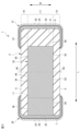
- 3 is a cross-sectional view taken along line III-III in FIG. 1.
- FIG. 4 is a cross-sectional view taken along line IV-IV in FIG.
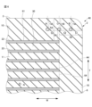
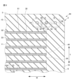
- FIG. 5 is an enlarged view of the box in FIG. 4 . 4 is a graph showing a first silicon concentration of a dielectric layer.
- FIG. 5 is an enlarged view of the box in FIG. 4 .
- FIG. 5 is an enlarged view of the box in FIG. 4 .
- 1 is a table showing the results of a humidity resistance load test.
- 1 is a table showing the results of a humidity resistance load test.
- FIG. 2 is a perspective view of a ceramic body core portion.
- FIG. 1 is a perspective view of a multilayer ceramic capacitor 1 according to an embodiment of the present invention.
- FIG. 1 shows a so-called two-terminal multilayer ceramic capacitor.
- the multilayer ceramic capacitor 1 includes a ceramic body 2 and terminal electrodes.
- the terminal electrodes include a first terminal electrode 20 and a second terminal electrode 21.
- the ceramic body 2 includes a plurality of laminated dielectric layers and a plurality of internal electrode layers.
- the internal electrode layers are laminated with the dielectric layers sandwiched between them.
- the shape of the ceramic body 2 is approximately a rectangular parallelepiped.
- the direction in which the dielectric layers and internal electrode layers are stacked is referred to as the stacking direction T.
- the direction perpendicular to the stacking direction T is referred to as the width direction W.
- the direction perpendicular to the stacking direction T and the width direction W is referred to as the length direction L.
- first body main surface 3 Of the two faces of the ceramic body 2 that face each other in the stacking direction T, one is called the first body main surface 3.
- the remaining surface is called the second body main surface 4.
- first body side surface 5 Of the two faces of the ceramic body 2 that face each other in the width direction W, one is called the first body side surface 5.
- the remaining surface is called the second body side surface 6.
- the cross section taken along line I-I in Figure 1 will be referred to as the LT cross section.
- the cross sections taken along lines II-II and III-III in Figure 1 will be referred to as the WT cross sections.
- the cross section taken along line IV-IV in Figure 1 will be referred to as the LW cross section.
- the portion where three faces of the ceramic body 2 intersect is called a corner.
- the portion where two faces of the ceramic body 2 intersect is called a ridge. It is preferable that the corners and ridges are rounded.
- Figure 2 is a cross-sectional view of line I-I in Figure 1.
- the first internal electrode layer 32 and the second internal electrode layer 33 are laminated via a dielectric layer 30.
- the dielectric layer 30 is formed of a ceramic dielectric.
- the ceramic dielectric that forms the dielectric layer 30 sandwiched between the first internal electrode layer 32 and the second internal electrode layer 33 is called the first ceramic dielectric.
- the internal electrode layers include a plurality of first internal electrode layers 32 and a plurality of second internal electrode layers 33.
- the first internal electrode layers 32 are internal electrode layers exposed at the first element body end surface 7.
- the second internal electrode layers 33 are internal electrode layers exposed at the second element body end surface 8.
- the first internal electrode layer 32 is divided into a first opposing electrode portion 34 and a first extension electrode portion 36.
- the first opposing electrode portion 34 is a portion that faces the second internal electrode layer 33.
- the first extension electrode portion 36 is a portion that is extended from the first opposing electrode portion 34 to the first element body end surface 7.
- the second internal electrode layer 33 is divided into a second opposing electrode portion 35 and a second extension electrode portion 37.
- the second opposing electrode portion 35 is a portion that faces the first internal electrode layer 32.
- the second extension electrode portion 37 is a portion that is extended from the second opposing electrode portion 35 to the second element body end surface 8.
- the divisions within the ceramic body 2 will be explained.
- the portion where the first internal electrode layer 32 and the second internal electrode layer 33 face each other in the stacking direction T is called the inner layer portion 11.
- the surfaces of the inner layer portion 11 are called as follows.
- the surface of the inner layer portion 11 in the stacking direction T is called the first inner layer main surface 61.
- the surface opposite the first inner layer main surface 61 is called the second inner layer main surface 62.
- the surface in the width direction W perpendicular to the first inner layer main surface 61 and the second inner layer main surface 62, from which the first internal electrode layer 32 and the second internal electrode layer 33 are drawn out, is called the first inner layer side surface 63.
- the surface opposite the first inner layer side surface 63, from which the first internal electrode layer 32 and the second internal electrode layer 33 are drawn out, is called the second inner layer side surface 64.
- the surface in the length direction L perpendicular to the first inner layer main surface 61, the second inner layer main surface 62, the first inner layer side surface 63, and the second inner layer side surface 64, from which the first internal electrode layer 32 is pulled out, is called the first inner layer end surface 65.
- the surface opposite the first inner layer end surface 65, from which the second internal electrode layer 33 is pulled out, is called the second inner layer end surface 66.
- the outer layer portion and side margin portion are referred to as follows.
- the portion formed of a ceramic dielectric and covering the first inner layer main surface 61 from the stacking direction T is referred to as the first outer layer portion 10.
- the portion formed of a ceramic dielectric and covering the second inner layer main surface 62 from the stacking direction T is referred to as the second outer layer portion 12.
- the portion formed of a ceramic dielectric and covering the inner layer portion 11, the first outer layer portion 10, and the second outer layer portion 12 from one side in the width direction W is referred to as the first side margin portion 16.
- the portion formed of a ceramic dielectric and covering the inner layer portion 11, the first outer layer portion 10, and the second outer layer portion 12 from the other side in the width direction W is referred to as the second side margin portion 18.
- the ceramic dielectric that forms the first outer layer 10, the second outer layer 12, the first side margin portion 16, and the second side margin portion 18 is called the second ceramic dielectric.
- the dielectric layer 30 is disposed on the first outer layer portion 10 and the second outer layer portion 12.
- the first internal electrode layer 32 and the second internal electrode layer 33 are not disposed on the first outer layer portion 10 and the second outer layer portion 12.
- the ceramic body 2 is divided in the longitudinal direction L into a first drawer section 13, a longitudinally opposing section 14, and a second drawer section 15.
- the longitudinal opposing portion 14 corresponds to the range of the longitudinal direction L of the inner layer portion 11.
- the first draw-out portion 13 is the portion between the longitudinal opposing portion 14 and the first element body end surface 7.
- the second draw-out portion 15 is the portion between the longitudinal opposing portion 14 and the second element body end surface 8.
- the longitudinal opposing portion 14 is a portion that corresponds to the opposing electrode portion of the internal electrode layer.
- the first extension portion 13 and the second extension portion 15 are portions that correspond to the extension electrode portions of the internal electrode layer.
- Figure 3 is a cross-sectional view taken along line II-II in Figure 1.
- Figure 4 is a cross-sectional view taken along line III-III in Figure 1. Both Figures 3 and 4 show a WT cross-section of the multilayer ceramic capacitor 1.
- Figure 3 is a WT cross-section at the second lead-out portion 15.
- Figure 4 is a WT cross-section at the longitudinal opposing portion 14.
- the first internal electrode layer 32 is not visible in the WT cross section of the second lead portion 15. Only the second internal electrode layer 33 is visible in the WT cross section. As a result, only the second internal electrode layer 33 is electrically connected to the second terminal electrode 21 at the second element body end surface 8.
- the second internal electrode layer 33 is not visible in the WT cross section of the first lead portion 13. Only the first internal electrode layer 32 is visible. At the first element body end surface 7, the first internal electrode layer 32 is electrically connected to the first terminal electrode 20.
- FIG. 1 the center position in the length direction L of the multilayer ceramic capacitor 1 is shown as length direction center position 90.
- Length 91 and length 92 shown in FIG. 1 are the same length.
- FIG. 4 is a WT cross section at length direction center position 90 of the multilayer ceramic capacitor 1.
- the ceramic body 2 is divided in the width direction W into a first side margin portion 16, a widthwise opposing portion 17, and a second side margin portion 18.
- the widthwise opposing portion 17 is the portion where the first internal electrode layer 32 and the second internal electrode layer 33 oppose each other in the stacking direction T.
- the first side margin portion 16 is the portion between the widthwise opposing portion 17 and the first element body side surface 5.
- the second side margin portion 18 is the portion between the widthwise opposing portion 17 and the second element body side surface 6.
- the widthwise opposing portion 17 is divided into a first outer layer portion 10, an inner layer portion 11, and a second outer layer portion 12 in the stacking direction T.
- the WT cross section at the longitudinal center position 90 is divided into a first side margin portion 16, a first outer layer portion 10, an inner layer portion 11, a second outer layer portion 12, and a second side margin portion 18.
- the portion of the ceramic body 2 excluding the first side margin portion 16 and the second side margin portion 18 is called the ceramic body core portion 40.
- the line showing the boundary between the ceramic body core portion 40 and the first side margin portion 16 is called the first boundary line 42.
- the line showing the boundary between the ceramic body core portion 40 and the second side margin portion 18 is called the second boundary line 44.
- the first boundary line 42 and the second boundary line 44 are imaginary lines.
- the first boundary line 42 and the second boundary line 44 are not recognized as actual lines.
- the first boundary line 42 can be drawn and determined by drawing a straight line passing through the end of the first internal electrode layer 32 on the first element side surface 5 side and the end of the second internal electrode layer 33 on the first element side surface 5 side.
- the second boundary line 44 can be drawn and determined by drawing a straight line passing through the end of the first internal electrode layer 32 on the second element side surface 6 side and the end of the second internal electrode layer 33 on the second element side surface 6 side.
- FIG. 5 is a cross-sectional view taken along line IV-IV in FIG. 1. Of the first internal electrode layer 32 and the second internal electrode layer 33, FIG. 5 shows the first internal electrode layer 32.
- first side margin portion 16 and the second side margin portion 18 are continuous from the first element body end surface 7 to the second element body end surface 8.
- the first opposing electrode portion 34 and the second opposing electrode portion 35 face each other via the dielectric layer 30, forming a capacitance. This allows the multilayer ceramic capacitor 1 to exhibit the characteristics of a capacitor.
- the first ceramic dielectric and the second ceramic dielectric include barium titanate, calcium titanate, and strontium titanate as main components.
- the dielectric ceramic may include an auxiliary component.
- the auxiliary component include rare earth oxides, silicon compounds, aluminum compounds, magnesium compounds, manganese compounds, iron compounds, chromium compounds, cobalt compounds, vanadium compounds, and nickel compounds.
- the ceramic dielectric may be a perovskite oxide represented by ABO3 , and may have a structure in which titanium is contained in the largest amount among the B-site elements.
- composition of the first ceramic dielectric and the composition of the second ceramic dielectric may be the same or different.
- each dielectric layer 30 is 0.3 ⁇ m or more and 10 ⁇ m or less.
- the preferred total number of dielectric layers 30 stacked in the ceramic body 2 is 15 to 2000.
- the main material of the internal electrode layer is a metal such as nickel, copper, silver, palladium, or gold.
- the material of the internal electrode layer may be an alloy containing at least one of the aforementioned metals, such as a silver-palladium alloy.
- the preferred thickness of the internal electrode layer is 0.2 ⁇ m or more and 2.0 ⁇ m or less.
- the preferred total number of first internal electrode layers 32 and second internal electrode layers 33 is 15 to 2000.
- the size of the ceramic body 2 is not particularly limited.
- the preferred length of the length direction L of the ceramic body 2 is 0.2 mm or more and 10 mm or less.
- the preferred length of the width direction W of the ceramic body 2 is 0.1 mm or more and 5 mm or less.
- the preferred length of the stacking direction T of the ceramic body 2 is 0.1 mm or more and 5 mm or less.
- the terminal electrodes include a first terminal electrode 20 and a second terminal electrode 21.
- the first terminal electrode 20 is a terminal electrode connected to the first internal electrode layer 32.
- the second terminal electrode 21 is a terminal electrode connected to the second internal electrode layer 33.
- the first terminal electrode 20 is arranged on the first element body end face 7, part of the first element body main surface 3, part of the second element body main surface 4, part of the first element body side surface 5, and part of the second element body side surface 6.
- the second terminal electrode 21 is arranged on the second element body end face 8, part of the first element body main surface 3, part of the second element body main surface 4, part of the first element body side surface 5, and part of the second element body side surface 6.
- the terminal electrode includes an external electrode film 22, a nickel plating film 24, and a tin plating film 25. These are arranged in the following order from the end face of the ceramic body 2: external electrode film 22, nickel plating film 24, tin plating film 25.
- the external electrode film 22 is disposed on and covers the end faces of the ceramic body 2.
- the external electrode film 22 extends from the end faces to a portion of the main surface and a portion of the side surface.
- the external electrode film 22 includes glass and metal.
- the glass includes, for example, boron and silicon.
- the metal includes, for example, at least one selected from copper, nickel, silver, palladium, silver-palladium alloy, gold, etc.
- the external electrode film 22 is formed by applying a conductive paste to the ceramic body 2 and firing it. This conductive paste includes glass and metal.
- the preferred thickness of the external electrode film 22 is, for example, 3 ⁇ m or more and 100 ⁇ m or less.
- the nickel plating film 24 is arranged to cover the external electrode film 22.
- the tin plating film 25 is arranged to cover the nickel plating film 24.
- solder When mounting the multilayer ceramic capacitor 1 on a substrate or the like, solder is used.
- the nickel plating film 24 prevents the external electrode film 22 from being eroded by the solder.
- the tin plating film 25 improves the wettability of the solder to the multilayer ceramic capacitor 1. As a result, it becomes easier to mount the multilayer ceramic capacitor 1 on a substrate, etc.
- the size of the multilayer ceramic capacitor 1 is not particularly limited.
- the preferred length in the length direction L of the multilayer ceramic capacitor 1 including the ceramic body 2 and the terminal electrodes is 0.2 mm or more and 10 mm or less.
- the preferred length in the stacking direction T of the multilayer ceramic capacitor 1 including the ceramic body 2 and the terminal electrodes is 0.1 mm or more and 5 mm or less.
- the preferred length in the width direction W of the multilayer ceramic capacitor 1 including the ceramic body 2 and the terminal electrodes is 0.1 mm or more and 10 mm or less.
- the amount of silicon contained in the dielectric layer 30 is explained.
- the silicon content per 100 mol of titanium at a specific position of the second ceramic dielectric is referred to as the first silicon concentration.
- the silicon content per 100 mol of titanium in a specific portion of the second ceramic dielectric is referred to as the second silicon concentration.
- the silicon content per 100 mol of titanium in the entire second ceramic dielectric forming the second side margin portion 18 are referred to as the second silicon concentration.
- the silicon content per 100 mol of titanium at a particular location in the first ceramic dielectric is referred to as the third silicon concentration.
- the first outer layer portion 10, the second outer layer portion 12, the first side margin portion 16, and the second side margin portion 18 are all formed of a second ceramic dielectric.
- the second silicon concentration of the first outer layer portion 10, the second outer layer portion 12, the first side margin portion 16, and the second side margin portion 18 is 1.0 mol% or more and 3.5 mol% or less.
- the length of the second side margin portion 18 in the width direction W is indicated as length 50. 1/3 of length 50 is indicated as length 52. Length 52 is referred to as the second length 52. Length 51 is 2/3 of length 50.
- FIG. 7 is a graph showing the first silicon concentration of the first outer layer portion 10 and the first silicon concentration of the second side margin portion 18.
- the X-axis of FIG. 7 indicates the position in the width direction W.
- the Y-axis of FIG. 7 indicates the first silicon concentration.
- Points A, O, and B shown in FIG. 7 are the outer layer position A, the origin O, and the side margin position B, respectively, as described based on FIG. 6.
- Point YA shown in FIG. 7 indicates the first silicon concentration at the outer layer position A.
- Point YB shown in FIG. 7 indicates the first silicon concentration at the side margin position B.
- the first silicon concentration YA and the first silicon concentration YB are 1.0 mol% or more and 3.5 mol% or less.
- the difference between the first silicon concentration YA and the first silicon concentration YB is 0.2 mol% or more and 2.5 mol% or less.
- FIG. 7 illustrates an example in which the first silicon concentration YA at the outer layer position A is smaller than the first silicon concentration YB at the side margin position B. If the difference between the first silicon concentration YA and the first silicon concentration YB is 0.2 mol% or more and 2.5 mol% or less, the first silicon concentration YA at the outer layer position A may be larger than the first silicon concentration YB at the side margin position B.
- Point YO shown in FIG. 7 indicates the first silicon concentration at the origin O.
- the first silicon concentration YO is equal to or greater than the first silicon concentration YA and equal to or less than the first silicon concentration YB, or equal to or less than the first silicon concentration YA and equal to or greater than the first silicon concentration YB.
- the first silicon concentration changes monotonically from the outer layer position A to the side margin position B, via the origin O.
- the first silicon concentration YO is preferably an intermediate value between the first silicon concentration YA and the first silicon concentration YB.
- the intermediate value is, for example, in the range of ((first silicon concentration YA + first silicon concentration YB)/2) ⁇ 5%.
- any position in the inner layer portion 11 is called the inner layer position N.
- the third silicon concentration at the inner layer position N is called the inner layer silicon concentration.
- a preferred relationship between the silicon concentration in the inner layer portion, the silicon concentration in the outer layer portion, and the silicon concentration in the side margin portion is as follows. Silicon concentration in inner layer ⁇ Silicon concentration in outer layer ⁇ Silicon concentration in side margin
- the first to third methods of measuring silicon concentrations are described with reference to FIG. 8.
- the first to third methods of measuring silicon concentrations are performed by composition analysis of the dielectric layer 30.
- the multilayer ceramic capacitor 1 is polished to expose the WT cross section at the center position 90 in the longitudinal direction.
- the first silicon concentration and the third silicon concentration are analyzed by composition analysis of the WT cross section using laser ablation ICP-MS (LA-ICP-MS).
- the spot shape for composition analysis is a square with its centers at the outer layer position A, the side margin position B, the inner layer position N, and the origin O.
- the length of one side of the square is 5 ⁇ m.
- the second silicon concentration is measured by EDX (energy dispersive X-ray spectroscopy).
- the measurement range is the entire first outer layer 10, second outer layer 12, first side margin 16, and second side margin 18 in a cross section parallel to the width direction and the stacking direction.
- the median particle size of the dielectric particles contained in the dielectric layer 30 at the origin O is 0.4 to 0.9 times the median particle size of the dielectric particles contained in the dielectric layer 30 at the side margin position B.
- the median particle size is also called the median diameter or D50.
- FIG. 9 is a diagram showing the measurement position and measurement range in measuring the particle size of dielectric particles.
- FIG. 9 is an enlarged view of the box 46 in FIG. 4.
- the particle size of the dielectric particles is measured using a scanning electron microscope (SEM). The measurement is performed on the WT cross section at the center position 90 in the longitudinal direction of the multilayer ceramic capacitor 1.
- the multilayer ceramic capacitor 1 is polished to the longitudinal center position 90 to expose the WT surface.
- An SEM image of the dielectric particles is taken at the WT cross section under conditions of a magnification of 30,000x, an acceleration voltage of 5 kV, and a field of view of 3 ⁇ m x 3 ⁇ m.
- Image processing software is used to recognize the edges of all dielectric particles contained in the SEM image, and the cross-sectional area of the dielectric particles is calculated.
- the equivalent circle diameter is calculated from the calculated cross-sectional area.
- the calculated equivalent circle diameter is regarded as the particle diameter. After excluding dielectric particles that are missing from the image, the diameters of all dielectric particles contained within the imaged range are measured, and the average value is calculated.
- the multilayer ceramic capacitor 1 of this embodiment can provide a multilayer ceramic capacitor 1 with higher moisture resistance reliability.
- the silicon concentration in the outer layer and the side margin is both 1.0 mol% or more and 3.5 mol% or less.
- the difference between the silicon concentration in the outer layer and the silicon concentration in the side margin is 0.2 mol% or more and 2.5 mol% or less.
- the origin silicon concentration is either equal to or greater than the silicon concentration in the outer layer and equal to or less than the silicon concentration in the side margin, or equal to or less than the silicon concentration in the outer layer and equal to or greater than the silicon concentration in the side margin.
- the silicon concentration in the outer layer and the silicon concentration in the side margin are within a predetermined preferred range, and the silicon concentration changes monotonically from the outer layer position A to the side margin position B.
- the moisture resistance reliability of the multilayer ceramic capacitor 1 is improved by the silicon concentrations being within the ranges described above on either side of the second boundary line 44 and exhibiting the change trend described above.
- the chip including the terminal electrodes has a length L of 1.6 mm, a length W of 0.8 mm, and a length T of 0.8 mm.
- the thickness of the dielectric layer 30 in the inner layer portion 11 is 0.5 ⁇ m
- the thickness of the internal electrode layer is 0.5 ⁇ m
- the number of layers of the dielectric layer 30 is 705.
- the thickness of the dielectric layer 30 here means the distance in the stacking direction T between adjacent internal electrode layers.
- the number of layers of the dielectric layer 30 is the number between adjacent internal electrode layers in the inner layer portion 11.
- the length 54 in the stacking direction T of the first outer layer portion 10 and the length in the stacking direction T of the second outer layer portion 12 are 45 ⁇ m.
- the length W of the first side margin portion 16 and the length W of the second side margin portion 18 are 30 ⁇ m.
- a humidity load test was conducted on 100 chips at a temperature of 125°C, humidity of 95% RH, and applied voltages of 2V, 4V, and 6V, and the insulation resistance IR was measured after 72 hours. Chips with LogIR ⁇ 4 were determined to be defective, and the defect rate was calculated from the number of defective chips. A calculated defect rate of less than 10% was deemed to be good. A defect rate of 10% or more was deemed to be defective.
- Figure 10 shows the results of the humidity load test for the chips of the embodiment and the comparative example.
- cases where the humidity load test results were good are marked with G.
- Cases where the humidity load test results were poor are marked with F.
- the silicon concentration in the outer layer portion and the silicon concentration in the side margin portion are 1.0 mol% or more and 3.5 mol% or less, The difference between the silicon concentration of the outer layer portion and the silicon concentration of the side margin portion is 0.2 mol% or more and 2.5 mol% or less,
- the origin silicon concentration was either equal to or greater than the outer layer silicon concentration and equal to or less than the side margin silicon concentration, or equal to or less than the outer layer silicon concentration and equal to or greater than the side margin silicon concentration, the results were good when the applied voltage was 2 V in the moisture resistance load test.
- the silicon concentration in each layer is less than the silicon concentration in the inner layer.
- the silicon concentration in the outer layer portion was smaller than the silicon concentration in the side margin portion, the results were good even when the applied voltage was 4 V in the humidity load test.
- Figure 11 shows the results of the humidity load test for the chips of the embodiment and the comparative example.
- the cases where the result of the humidity load test is good are marked with G.
- the cases where the result of the humidity load test is poor are marked with F.
- the median particle size of the dielectric particles contained in the dielectric layer 30 at the origin O is 0.4 to 0.9 times the median particle size of the dielectric particles contained in the dielectric layer 30 at the side margin position B, i.e., the side margin portion.
- the ratio of length 52 to length 50 in the width direction W of the second side margin portion 18 is not limited to 1/3; for example, the ratio may be 1/4. Furthermore, length 52 does not have to be determined as a ratio to length 50. For example, length 52 may be a constant value, such as 10 ⁇ m. Length 52 can be determined appropriately depending on, for example, the length of the side margin portion in the width direction W.
- the reason why the moisture resistance reliability of the multilayer ceramic capacitor 1 of this embodiment is improved is believed to be as follows.
- the desired amount of silicon is contained in the dielectric layer 30 from the outer layer portion to the side margin portion.
- the amount of silicon changes monotonically from the side margin portion to the outer layer portion. This improves the bonding strength between the outer layer portion and the side margin portion. As a result, the moisture resistance reliability is improved.
- the relationship between the median particle size of the dielectric particles and the moisture resistance reliability is considered as follows.
- the particle size of the dielectric particles in the dielectric layer 30 is preferably uniform. This is because distortion is unlikely to occur in the dielectric layer 30.
- the median particle size of the dielectric particles contained in the dielectric layer 30 near the origin O is 0.4 to 0.9 times the median particle size of the dielectric particles contained in the dielectric layer 30 in the side margin portion.
- the ratio between the median particle size of the dielectric particles in the vicinity of the interface between the outer layer portion and the side margin portion, in other words, in a predetermined range from the origin O in the direction of the side margin position B and the direction of the outer layer position A, and the median particle size of the dielectric particles in the side margin portion is within a predetermined range. Therefore, steps in the arrangement of the dielectric particles and distortion between the dielectric particles are unlikely to occur in the dielectric layer 30. Therefore, the multilayer ceramic capacitor 1 of this embodiment has improved moisture resistance reliability.
- the ceramic element core portion precursor 040 is a precursor of the ceramic element before the dielectric sheets for the side margin portions are arranged.
- the precursor means before firing.
- the portion of the ceramic element excluding the side margin portions is called the ceramic element core portion.
- a dielectric sheet for the ceramic body core and a conductive paste for the internal electrode layers are prepared.
- the dielectric sheet and the conductive paste for the internal electrode layers contain a binder and a solvent.
- the binder and the solvent may be a known organic binder and organic solvent.
- a conductive paste for the internal electrode layer is printed in a predetermined pattern on the dielectric sheet. This forms an internal electrode layer pattern on the dielectric sheet. Examples of printing methods include screen printing and gravure printing.
- a predetermined number of dielectric sheets that do not have an internal electrode layer pattern printed on them are stacked.
- the stacked layers become layers that include an outer layer portion on one side.
- Dielectric sheets that have an internal electrode layer pattern printed on them are stacked in sequence on top of them.
- the stacked layers become layers that include an inner layer portion.
- a predetermined number of dielectric sheets that do not have an internal electrode layer pattern printed on them are stacked on top of them.
- the stacked layers become layers that include an outer layer portion on the other side.
- the laminated sheets are pressed in the stacking direction to produce a laminated block.
- An example of a pressing method is isostatic pressing.
- the laminated block is cut.
- the conductive paste corresponding to the internal electrode layers is exposed on both sides in the width direction W.
- the cut laminated block is called the ceramic element core precursor 040.
- Figure 12 is a perspective view of the ceramic element core precursor 040.
- Dielectric sheets for forming side margins are placed on both sides of the ceramic body core precursor 040 in the width direction W.
- the ceramic body 2 is then formed through firing and cutting.
- each part of the ceramic body core precursor 040 is given a component number with a "0" added before the corresponding component number in the ceramic body 2.
- part 032 in the ceramic body core precursor 040 corresponds to the first internal electrode layer 32 in the ceramic body 2.
- the dielectric material may be the same as the dielectric material for the ceramic body core portion.
- Additives may be added to the dielectric powder obtained from this dielectric material.
- the dielectric sheet for the side margin portion may have a two-layer structure including an inner layer in contact with the ceramic body core portion precursor 040 and an outer layer. The inner layer and the outer layer may contain different solvents and additives.
- silicon is added to at least the dielectric sheet for the side margin portion.
- the silicon concentration of the dielectric sheet for the ceramic element core portion is made different from the silicon concentration of the dielectric sheet for the side margin portion.
- the silicon concentration of the dielectric sheet for the side margin portion is made higher than the silicon concentration of the dielectric sheet for the ceramic element core portion.
- the silicon concentration may be different between the dielectric sheet corresponding to the inner layer and the dielectric sheet corresponding to the outer layer.
- the dielectric sheet for the side margin portion is pressed against the ceramic element core portion precursor 040. Then, by punching, a layer that will become the side margin portion is formed. Next, similarly, the dielectric sheet for the inner layer portion is opposed to the other side of the ceramic element core portion precursor 040, and the dielectric sheet for the side margin portion is pressed against it. Then, by punching, a layer that will become the side margin portion on the other side is formed. Note that punching may be performed after the dielectric sheets for the side margin portion have been pressed against both sides of the ceramic element core portion precursor 040.
- the laminated chip on which the layer that will become the side margin portion is formed is degreased under predetermined conditions in a nitrogen atmosphere. After that, the laminated chip is fired at a predetermined temperature in a nitrogen-hydrogen-water vapor mixed atmosphere to obtain a sintered ceramic body.
- the firing process may be performed at a temperature at which the laminated chip is sufficiently densified. For example, the firing process may be performed under conditions of holding the temperature at 1200°C to 1300°C for 0 minutes to 30 minutes.
- the firing process may be performed in an atmosphere in which the main component compound such as BaTiO 3 is not reduced and the oxidation of the conductive material is suppressed. For example, the firing process may be performed in a N 2 -H 2 -H 2 O air flow with an oxygen partial pressure of 1.8 ⁇ 10 -9 to 8.7 ⁇ 10 -10 MPa.
- an annealing process may be performed after the firing process.
- Terminal electrodes are formed on each of the two end faces of the sintered ceramic body.
- the multilayer ceramic capacitor 1 is manufactured.
- the formation of the terminal electrodes may be performed by a known method. For example, a conductive paste containing a conductive component such as Cu or Ni as a main component is applied and baked on the end faces exposed by pulling out the internal electrodes of the body portion to form a base layer.
- the base layer may be formed by applying a conductive paste to both end faces of the green body portion before firing, followed by a firing process. After the base layer is formed, electrolytic plating may be performed to form a plating film of Ni, Sn, or the like on the surface of the base layer. This completes the manufacture of the multilayer ceramic capacitor.
- the silicon concentration of the dielectric sheet for the ceramic body core portion is different from the silicon concentration of the dielectric sheet for the side margin portion. Therefore, silicon moves during firing. As a result, a silicon concentration gradient can be formed between the outer layer portion and the side margin portion.
- a content rate of silicon per 100 mol of titanium in the entire second ceramic dielectric forming the second side margin portion is defined as a second silicon concentration
- the second silicon concentration of the first outer layer portion, the second outer layer portion, the first side margin portion, and the second side margin portion is 1.0 mol% or more and 3.5 mol% or less.
- the content ratio of silicon per 100 mol of titanium at a specific position of the first ceramic dielectric is defined as a third silicon concentration
- the first silicon concentration at the outer layer position relative to the origin is smaller than the first silicon concentration at the side margin position relative to the origin;
- the third silicon concentration of the inner layer portion is lower than the first silicon concentration of the outer layer position relative to the origin.
- a median particle size of the dielectric particles contained in the dielectric layer in the vicinity of the origin is 0.4 to 0.9 times a median particle size of the dielectric particles contained in the dielectric layer at a side margin position relative to the origin, ⁇ 1>
- Multilayer ceramic capacitor 2 Ceramic body 3 First body main surface 4 Second body main surface 5 First body side surface 6 Second body side surface 7 First body end surface 8 Second body end surface 10 First outer layer portion 11 Inner layer portion 12 Second outer layer portion 13 First lead portion 14 Lengthwise opposing portion 15 Second lead portion 16 First side margin portion 18 Second side margin portion 20 First terminal electrode 21 Second terminal electrode 22 External electrode film 24 Nickel plating film 25 Tin plating film 30 Dielectric layer 32 First internal electrode layer 33 Second internal electrode layer 34 First opposing electrode portion 35 Second opposing electrode portion 36 First lead electrode portion 37 Second lead electrode portion 40 Ceramic body core portion precursor 42 First boundary line 44 Second boundary line 61 First inner layer main surface 62 Second inner layer main surface 63 First inner layer side surface 64 Second inner layer side surface 65 First inner layer end surface 66 Second inner layer end surface 90 Lengthwise center positions 91, 92 Length A Outer layer position B Side margin position O Origin L Lengthwise direction T Stacking direction W Width direction
Landscapes
- Engineering & Computer Science (AREA)
- Power Engineering (AREA)
- Manufacturing & Machinery (AREA)
- Microelectronics & Electronic Packaging (AREA)
- Ceramic Engineering (AREA)
- Chemical & Material Sciences (AREA)
- Inorganic Chemistry (AREA)
- Fixed Capacitors And Capacitor Manufacturing Machines (AREA)
- Ceramic Capacitors (AREA)
Priority Applications (3)
| Application Number | Priority Date | Filing Date | Title |
|---|---|---|---|
| JP2025542751A JPWO2025047103A1 (https=) | 2023-08-31 | 2024-07-01 | |
| CN202480054657.8A CN121729750A (zh) | 2023-08-31 | 2024-07-01 | 层叠陶瓷电容器 |
| US19/262,567 US20250336612A1 (en) | 2023-08-31 | 2025-07-08 | Multilayer ceramic capacitor |
Applications Claiming Priority (2)
| Application Number | Priority Date | Filing Date | Title |
|---|---|---|---|
| JP2023141185 | 2023-08-31 | ||
| JP2023-141185 | 2023-08-31 |
Related Child Applications (1)
| Application Number | Title | Priority Date | Filing Date |
|---|---|---|---|
| US19/262,567 Continuation US20250336612A1 (en) | 2023-08-31 | 2025-07-08 | Multilayer ceramic capacitor |
Publications (1)
| Publication Number | Publication Date |
|---|---|
| WO2025047103A1 true WO2025047103A1 (ja) | 2025-03-06 |
Family
ID=94818944
Family Applications (1)
| Application Number | Title | Priority Date | Filing Date |
|---|---|---|---|
| PCT/JP2024/023832 Pending WO2025047103A1 (ja) | 2023-08-31 | 2024-07-01 | 積層セラミックコンデンサ |
Country Status (4)
| Country | Link |
|---|---|
| US (1) | US20250336612A1 (https=) |
| JP (1) | JPWO2025047103A1 (https=) |
| CN (1) | CN121729750A (https=) |
| WO (1) | WO2025047103A1 (https=) |
Citations (2)
| Publication number | Priority date | Publication date | Assignee | Title |
|---|---|---|---|---|
| JP2019197790A (ja) * | 2018-05-09 | 2019-11-14 | 太陽誘電株式会社 | 積層セラミックコンデンサ及びその製造方法 |
| JP2020031242A (ja) * | 2019-12-02 | 2020-02-27 | 株式会社村田製作所 | 積層セラミックコンデンサ |
-
2024
- 2024-07-01 CN CN202480054657.8A patent/CN121729750A/zh active Pending
- 2024-07-01 WO PCT/JP2024/023832 patent/WO2025047103A1/ja active Pending
- 2024-07-01 JP JP2025542751A patent/JPWO2025047103A1/ja active Pending
-
2025
- 2025-07-08 US US19/262,567 patent/US20250336612A1/en active Pending
Patent Citations (2)
| Publication number | Priority date | Publication date | Assignee | Title |
|---|---|---|---|---|
| JP2019197790A (ja) * | 2018-05-09 | 2019-11-14 | 太陽誘電株式会社 | 積層セラミックコンデンサ及びその製造方法 |
| JP2020031242A (ja) * | 2019-12-02 | 2020-02-27 | 株式会社村田製作所 | 積層セラミックコンデンサ |
Also Published As
| Publication number | Publication date |
|---|---|
| JPWO2025047103A1 (https=) | 2025-03-06 |
| US20250336612A1 (en) | 2025-10-30 |
| CN121729750A (zh) | 2026-03-24 |
Similar Documents
| Publication | Publication Date | Title |
|---|---|---|
| US20130258546A1 (en) | Multilayer ceramic electronic component and fabrication method thereof | |
| CN115483030B (zh) | 层叠陶瓷电子部件 | |
| US10170243B2 (en) | Multilayer ceramic capacitor | |
| KR20130084853A (ko) | 적층 세라믹 전자부품 및 이의 제조방법 | |
| JP6980873B2 (ja) | 積層セラミックコンデンサ | |
| JP7517260B2 (ja) | 積層セラミック電子部品 | |
| US9281121B2 (en) | Multilayer ceramic electronic component and manufacturing method thereof | |
| JP2018181956A (ja) | 積層セラミックコンデンサ | |
| US11315730B2 (en) | Multilayer electronic component | |
| JP2024055118A (ja) | セラミック電子部品およびその製造方法 | |
| US12272497B2 (en) | Multilayer electronic component | |
| US12542239B2 (en) | Multilayer electronic component and method for manufacturing multilayer electronic component | |
| JP7209072B2 (ja) | 積層セラミックコンデンサ | |
| JP7585990B2 (ja) | 積層セラミック電子部品 | |
| CN117716457A (zh) | 层叠陶瓷电容器 | |
| JP6766225B2 (ja) | 積層セラミックコンデンサ | |
| WO2025047103A1 (ja) | 積層セラミックコンデンサ | |
| CN119816908A (zh) | 层叠陶瓷电容器 | |
| KR20250002659A (ko) | 적층 세라믹 콘덴서 | |
| WO2023243159A1 (ja) | 積層セラミックコンデンサ | |
| KR20240155921A (ko) | 적층 세라믹 콘덴서 | |
| JP2023119110A (ja) | 積層セラミックコンデンサ | |
| JP4677798B2 (ja) | 電子機器 | |
| US20250372311A1 (en) | Multilayer ceramic capacitor | |
| US20260011499A1 (en) | Multilayer ceramic electronic device and manufacturing method of the same |
Legal Events
| Date | Code | Title | Description |
|---|---|---|---|
| 121 | Ep: the epo has been informed by wipo that ep was designated in this application |
Ref document number: 24859148 Country of ref document: EP Kind code of ref document: A1 |
|
| ENP | Entry into the national phase |
Ref document number: 2025542751 Country of ref document: JP Kind code of ref document: A |
|
| WWE | Wipo information: entry into national phase |
Ref document number: 2025542751 Country of ref document: JP |