WO2025032692A1 - 電力変換装置及び冷凍サイクル装置 - Google Patents
電力変換装置及び冷凍サイクル装置 Download PDFInfo
- Publication number
- WO2025032692A1 WO2025032692A1 PCT/JP2023/028778 JP2023028778W WO2025032692A1 WO 2025032692 A1 WO2025032692 A1 WO 2025032692A1 JP 2023028778 W JP2023028778 W JP 2023028778W WO 2025032692 A1 WO2025032692 A1 WO 2025032692A1
- Authority
- WO
- WIPO (PCT)
- Prior art keywords
- current
- compensation current
- voltage
- power conversion
- conversion device
- Prior art date
- Legal status (The legal status is an assumption and is not a legal conclusion. Google has not performed a legal analysis and makes no representation as to the accuracy of the status listed.)
- Pending
Links
Images



Classifications
-
- H—ELECTRICITY
- H02—GENERATION; CONVERSION OR DISTRIBUTION OF ELECTRIC POWER
- H02M—APPARATUS FOR CONVERSION BETWEEN AC AND AC, BETWEEN AC AND DC, OR BETWEEN DC AND DC, AND FOR USE WITH MAINS OR SIMILAR POWER SUPPLY SYSTEMS; CONVERSION OF DC OR AC INPUT POWER INTO SURGE OUTPUT POWER; CONTROL OR REGULATION THEREOF
- H02M1/00—Details of apparatus for conversion
- H02M1/12—Arrangements for reducing harmonics from AC input or output
-
- H—ELECTRICITY
- H02—GENERATION; CONVERSION OR DISTRIBUTION OF ELECTRIC POWER
- H02M—APPARATUS FOR CONVERSION BETWEEN AC AND AC, BETWEEN AC AND DC, OR BETWEEN DC AND DC, AND FOR USE WITH MAINS OR SIMILAR POWER SUPPLY SYSTEMS; CONVERSION OF DC OR AC INPUT POWER INTO SURGE OUTPUT POWER; CONTROL OR REGULATION THEREOF
- H02M7/00—Conversion of AC power input into DC power output; Conversion of DC power input into AC power output
- H02M7/02—Conversion of AC power input into DC power output without possibility of reversal
- H02M7/04—Conversion of AC power input into DC power output without possibility of reversal by static converters
- H02M7/06—Conversion of AC power input into DC power output without possibility of reversal by static converters using discharge tubes without control electrode or semiconductor devices without control electrode
-
- H—ELECTRICITY
- H02—GENERATION; CONVERSION OR DISTRIBUTION OF ELECTRIC POWER
- H02M—APPARATUS FOR CONVERSION BETWEEN AC AND AC, BETWEEN AC AND DC, OR BETWEEN DC AND DC, AND FOR USE WITH MAINS OR SIMILAR POWER SUPPLY SYSTEMS; CONVERSION OF DC OR AC INPUT POWER INTO SURGE OUTPUT POWER; CONTROL OR REGULATION THEREOF
- H02M7/00—Conversion of AC power input into DC power output; Conversion of DC power input into AC power output
- H02M7/42—Conversion of DC power input into AC power output without possibility of reversal
- H02M7/44—Conversion of DC power input into AC power output without possibility of reversal by static converters
- H02M7/48—Conversion of DC power input into AC power output without possibility of reversal by static converters using discharge tubes with control electrode or semiconductor devices with control electrode
Definitions
- This disclosure relates to a power conversion device and a refrigeration cycle device that convert a power supply voltage applied from an AC power supply into a drive voltage for a load.
- Leakage current is a high-frequency current that flows through stray capacitance between the compressor (load) and earth potential due to switching control of the switching elements equipped in the inverter.
- the leakage current that flows to earth potential returns to the refrigeration cycle device (the source) via the ground point where the AC power supply is grounded, and is therefore also called "common mode current.”
- Patent Document 1 discloses a technology that monitors a current corresponding to a common mode current leaking from a load, and when the instantaneous value, average value, or peak value of the monitored current is greater than a threshold value, controls a switch to close and outputs a compensation current to compensate for the common mode current.
- the compensation current generating section which generates the compensation current, is equipped with an amplifying element.
- an amplifying element In order to stably output the compensation current and to ensure the impedance seen from the detection section to the compensation current generating section, a resistor is connected to the amplifying element. However, if the resistance value of this resistor is not set appropriately according to the type of amplifying element, the operating time of the amplifying element will be delayed, which can hinder the compensation operation, especially in the high frequency range.
- the present disclosure has been made in consideration of the above, and aims to obtain a power conversion device that can prevent the compensation operation in the high frequency range in the compensation current generating section from being impaired.
- the power conversion device is a power conversion device that converts a power supply voltage applied from an AC power supply into a drive voltage for a load, and includes a detection unit, a compensation current generation unit, an adjustment circuit unit, and an injection unit.
- the detection unit detects a physical quantity that is correlated with a common mode current flowing inside the power conversion device via an earth potential that is a reference for the power supply voltage.
- the compensation current generation unit generates a compensation current for canceling the common mode current based on the physical quantity detected by the detection unit.
- the adjustment circuit unit adjusts the rise start time of the compensation current in the compensation current generation unit.
- the injection unit injects the compensation current into the earth potential.
- the circuit constants of the adjustment circuit unit and the compensation current generation unit are set so that the first delay time is smaller than the second delay time.
- the first delay time is the time from when the adjustment circuit unit outputs a signal for operating the compensation current generation unit to when the injection unit starts injecting the compensation current into the earth potential.
- the second delay time is the time from when the common mode current based on the physical quantity detected by the detection unit starts to rise to when it reaches a peak.
- the power conversion device disclosed herein has the effect of preventing the compensation operation in the compensation current generating section in the high frequency range from being impeded.
- FIG. 1 is a diagram showing a configuration example of a power conversion device according to a first embodiment
- FIG. 10 is a diagram for explaining response characteristics when an amplifying element in a compensation current generating unit according to the first embodiment is a voltage-driven element.
- FIG. 1 is a diagram for explaining the characteristics of the operation of the power conversion device according to the first embodiment
- FIG. 10 is a diagram for explaining a method for calculating a first delay time when an amplifying element provided in a compensation current generating unit according to the first embodiment is a voltage-driven element
- FIG. 10 is a diagram for explaining a method for calculating a first delay time when an amplifying element provided in a compensation current generating unit according to the first embodiment is a current-driven element
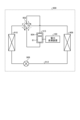
- FIG. 1 is a diagram showing a configuration example of a refrigeration cycle device according to a second embodiment
- Embodiment 1. 1 is a diagram showing a configuration example of a power conversion device 100 according to embodiment 1.
- the power conversion device 100 according to embodiment 1 drives a load 60 by converting a power supply voltage applied from an AC power supply 50 into a drive voltage for a motor 61 connected to the load 60.
- an example of the load 60 is a compressor or a fan.
- the midpoint 54 of the AC power supply 50 is grounded to an earth potential 51.
- the earth potential 51 is the potential of a ground wire or ground surface (not shown) and serves as the reference potential of the power supply voltage.
- the AC power supply 50 is shown as a single-phase three-wire system in FIG. 1, this is not limiting.
- the AC power supply 50 may be a single-phase two-wire system, a three-phase three-wire system, or a three-phase four-wire system.
- the power distribution system of the AC power supply 50 is determined according to the specifications of the refrigeration cycle device.
- the power conversion device 100 includes a noise filter 11, a rectifier 12, a smoothing capacitor 13, an inverter 15, and a canceller 80.
- the noise filter 11 is a passive filter composed of passive elements such as an inductor and a capacitor.
- the noise filter 11 is electrically connected to an earth potential 52.
- the noise filter 11 is disposed between an AC power source 50 and the rectifier 12, and operates to reduce noise currents flowing in and out of the power conversion device 100.
- the rectifier 12 rectifies the power supply voltage applied from the AC power source 50.
- the smoothing capacitor 13 is disposed between a DC bus 71 and a DC bus 72, which are electrical wiring for electrically connecting the rectifier 12 and the inverter 15, and smoothes and holds the rectified voltage rectified by the rectifier 12.
- the inverter 15 is a conversion unit that converts the rectified voltage rectified by the rectifier 12 into a drive voltage for the load 60. Specifically, the inverter 15 has multiple switching elements 14 and converts the rectified voltage rectified by the rectifier 12 into a drive voltage for the motor 61 to drive the motor 61.
- the canceller 80 also includes a detection unit 20, an adjustment circuit unit 30, a compensation current generation unit 38, and an injection unit 40.
- the detection unit 20 includes a first coil 21 and a second coil 22 that is magnetically coupled to the first coil 21.
- the first coil 21 includes two windings 21a and 21b.
- the winding 21a is arranged on the power line 18, and the winding 22a is arranged on the power line 19.
- the power lines 18 and 19 are electrical wiring for electrically connecting the noise filter 11 and the rectification unit 12.
- the second coil 22 includes two windings 22a and 22b that are magnetically coupled to the winding 21b.
- the first coil 21 is a main circuit winding
- the second coil 22 is an auxiliary winding.
- the black circles in the figure are symbols indicating the polarity of the voltage generated in each winding. For example, if the voltage induced in winding 21b is higher on the black circle side, the voltage induced in windings 22a and 22b will be higher on the black circle side. Therefore, induced voltages of opposite polarity are always generated in windings 22a and 22b.
- the adjustment circuit unit 30 includes termination resistors 31a and 31b and adjustment resistors 33a and 33b.
- the adjustment circuit unit 30 outputs a signal for operating the compensation current generation unit 38 via the adjustment resistors 33a and 33b.
- the compensation current generation unit 38 includes MOSFETs (Metal-Oxide-Semiconductor Field-Effect Transistors) 35a and 35b, which are amplifying elements.
- the termination resistor 31a, the adjustment resistor 33a, and the MOSFET 35a are provided corresponding to the winding 22a, and the termination resistor 31b, the adjustment resistor 33b, and the MOSFET 35b are provided corresponding to the winding 22b.
- the MOSFETs 35a and 35b are an example of a voltage-driven element, but a current-driven element may be used instead of the MOSFETs 35a and 35b.
- An example of a current-driven element is a bipolar transistor.
- the injection unit 40 includes a resistor 41 and a capacitor 42 connected in series to the resistor 41.
- the injection unit 40 is electrically connected to earth potential 52. Note that in FIG. 1, the connection order of the resistor 41 and the capacitor 42 in the injection unit 40 may be reversed from that shown in the figure. That is, the resistor 41 may be disposed on the side of the earth potential 52. Also, the injection unit 40 does not need to include both the resistor 41 and the capacitor 42, and it is sufficient if it includes at least one of the resistor 41 and the capacitor 42.
- the inverter 15 When the inverter 15 performs a switching operation, the inverter 15 generates power. At this time, the inverter 15 becomes a noise source, that is, a source of noise power, and a common mode current flows inside the power conversion device 100.
- the common mode current here means a leakage current that flows through the parasitic capacitance 62 between the load 60 and the earth potential 63. Since the common mode current flows inside the power conversion device 100, it also flows through the power lines 18 and 19.
- the windings 22a and 22b of the detection unit 20 detect a physical quantity that is correlated with the common mode current flowing through the power lines 18 and 19.
- the detection voltage of the winding 22a is generated across the termination resistor 31a, and the voltage of the termination resistor 31a is applied to the MOSFET 35a via the adjustment resistor 33a.
- the detection voltage of the winding 22a is an example of a physical quantity that is correlated with the common mode current.
- the MOSFET 35a When the voltage of the termination resistor 31a exceeds the threshold voltage of the MOSFET 35a, the MOSFET 35a becomes conductive. When the MOSFET 35a becomes conductive, the connection point 37 between the MOSFETs 35a and 35b is electrically connected to the high-potential DC bus 71 via the conductive MOSFET 35a, and a compensation current flows from the connection point 37 toward the earth potential 52 via the injection unit 40. This direction cancels out the common mode current, and the compensation current flowing via the injection unit 40 reduces the common mode current.
- the detection voltage of winding 22b is generated across termination resistor 31b, and the voltage of termination resistor 31b is applied to MOSFET 35b via adjustment resistor 33b.
- MOSFET 35b becomes conductive.
- node 37 is electrically connected to the low-potential DC bus 72 via the conductive MOSFET 35b, and a compensation current flows from earth potential 52 toward node 37 via injection unit 40.
- This direction is the opposite to when MOSFET 35a is conductive, but because winding 22a and winding 22b are connected with opposite polarity, this direction cancels out the common mode current. Therefore, even when MOSFET 35b is conductive, the common mode current is reduced by the compensation current flowing through injection unit 40.
- the detection unit 20 detects a physical quantity that is correlated with the common mode current flowing between the noise filter 11 and the rectification unit 12, and the compensation current generation unit 38 that generates a compensation current based on the detected physical quantity is connected between the rectification unit 12 and the inverter 15, which is the source of noise power. Therefore, the detection unit 20 and the compensation current generation unit 38 are configured as a feedback system when viewed from the inverter 15.
- the detection unit 20 and the compensation current generation unit 38 can generate compensation currents of both polarities, but common mode current reduction is also possible with a compensation current of one polarity. Therefore, when a compensation current of one polarity is generated, one of the windings 22a, 22b of the detection unit 20 can be omitted.
- one of the sets of the termination resistor 31a, the adjustment resistor 33a, and the MOSFET 35a, and the set of the termination resistor 31b, the adjustment resistor 33b, and the MOSFET 35b in the compensation current generation unit 38 corresponding to the omitted windings of the windings 22a, 22b can be omitted.
- the detection unit 20 detects a physical quantity that is correlated with the common mode current flowing inside the power conversion device 100 via the earth potential 51 that serves as the reference for the power supply voltage. Furthermore, the compensation current generation unit 38 generates a compensation current for canceling the common mode current based on the physical quantity detected by the detection unit 20. Then, the injection unit 40 injects the compensation current output from the compensation current generation unit 38 into the earth potential 52.
- Figure 2 is a diagram used to explain the response characteristics when the amplifying element in the compensation current generating unit 38 according to the first embodiment is a voltage-driven element.
- FIG. 2 shows the waveform of the voltage Vc applied to the gate of a voltage-driven element when a voltage of amplitude E is applied to the voltage-driven element.
- the solid line is the waveform of the voltage Vc when the time constant ⁇ is small
- the dashed line is the waveform of the voltage Vc when the time constant ⁇ is medium
- the dashed line is the waveform of the voltage Vc when the time constant ⁇ is large.
- the horizontal axis is time.
- the operating threshold when the voltage-driven element turns on is Vth
- the time constant ⁇ is large, it takes a long time for the voltage Vc to reach the operating threshold Vth, as shown in Figure 2. Therefore, if the resistance value R is large, a large delay occurs in turning on the voltage-driven element. If this time delay becomes large, the compensation operation in the high frequency range is hindered, and the compensation performance for high frequency common mode currents deteriorates.
- FIG. 3 is a diagram illustrating the characteristics of the operation of the power conversion device 100 according to the first embodiment.
- the horizontal axis in FIG. 3 represents time.
- the waveform of the common mode current is shown by a dashed line, and the waveform of the through current is shown by a solid line.
- the middle part shows the waveform of the gate voltage.
- the lower part shows the waveform of the compensation current.
- the common mode current shown in the upper part is a current of a common mode component that attempts to flow inside the power conversion device 100 when the canceller 80 is not operating.
- the gate voltage shown in the middle part is a voltage that is applied to the gate of the MOSFET 35 by the compensation current generating unit 38 in the canceller 80 when the canceller 80 operates and the common mode current shown in the upper part attempts to flow.
- the compensation current shown in the lower part is a compensation current that is injected into the earth potential 52 by the injection unit 40 in the canceller 80 when the canceller 80 operates.
- the compensation current is a current of opposite phase to the common mode current.
- the flow current shown in the upper part represents the difference between the common mode current and the compensation current, and is the residual component of the common mode current that remains uncompensated.
- Ts1 is the time when the compensation current starts to flow based on the time when the common mode current starts to rise, and is referred to as the "first delay time” in this paper.
- the first delay time Ts1 is the time from when the adjustment circuit unit 30 applies a gate voltage to the compensation current generation unit 38 to when the injection unit 40 starts injecting the compensation current into the earth potential 52.
- Ts2 is the time from when the common mode current starts to rise until it reaches its peak, and is referred to as the "second delay time" in this paper.
- the second delay time Ts2 is the time from when the common mode current based on the physical quantity detected by the detection unit 20 starts to rise until it reaches its peak.
- the circuit constants of the adjustment circuit unit 30 and the compensation current generating unit 38 are set so that the first delay time Ts1 is shorter than the second delay time Ts2 so that the compensation operation in the high frequency range is not hindered.
- the circuit constants referred to here include the adjustment resistor 33 which is the resistive element of the adjustment circuit unit 30, the input capacitance which is the capacitive element of the MOSFET 35, the operating threshold of the MOSFET 35, etc.
- the first coil 21 in the detection unit 20 will be called the “main circuit winding” and the second coil 22 will be called the “auxiliary winding.”
- the method for calculating the first delay time Ts1 differs depending on whether the amplifying element is a voltage-driven element or a current-driven element, so they will be described separately.
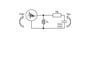
- FIG. 4 is a diagram illustrating a method for calculating the first delay time Ts1 when the amplifying element provided in the compensation current generating unit 38 according to the first embodiment is a voltage-driven element.
- FIG. 4 shows an equivalent circuit when one corresponding voltage-driven element is viewed from one of the auxiliary windings in the detection unit 20.
- a MOSFET is assumed as the voltage-driven element.
- Vdet is the detection voltage by the detection unit 20
- Rg is the resistance value of the gate resistor connected to the gate of the voltage-driven element
- Ciss is the input capacitance of the voltage-driven element
- Vgs is the gate-source voltage of the voltage-driven element
- Vth is the operating threshold when the voltage-driven element turns on.
- ZL is the impedance when looking at the detection unit 20 from the voltage-driven element, and is referred to here as the "winding impedance.”
- the impedance Zi when looking at the voltage-driven element from the detection unit 20 can be expressed by the following equation (1).
- Zciss is the impedance of the input capacitance Ciss
- N1 is the number of turns of the main circuit winding
- N2 is the number of turns of the auxiliary winding.
- the operation mode of the detection unit 20 changes depending on the magnitude relationship between the impedance Zi and the winding impedance ZL.
- Transformer operation is an operation in which the voltage induced in the auxiliary winding is directly proportional to the turns ratio between the main circuit winding and the auxiliary winding.
- the turns ratio here is the ratio of the turns N2 of the auxiliary winding to the turns N1 of the main circuit winding.
- Current transformer operation is an operation in which the current flowing through the auxiliary winding is inversely proportional to the turns ratio between the main circuit winding and the auxiliary winding.
- the detection unit 20 When impedance Zi is greater than the winding impedance ZL, the detection unit 20 operates as a transformer, and conversely, when winding impedance ZL is greater than impedance Zi, the detection unit 20 operates as a current transformer.
- the input capacitance Ciss of the voltage-driven element is a small value, and therefore the impedance Zciss is large. Therefore, when the amplifying element is a voltage-driven element, most of the detection current flows through the auxiliary winding, and the detector 20 basically operates as a transformer.
- the first delay time Ts1 can be calculated as the time from the reference time when the detection voltage of the detection unit 20 is applied to the voltage-driven element until the response waveform of the gate-source voltage Vgs reaches the operating threshold Vth.
- FIG. 5 is a diagram for explaining a method for calculating the first delay time Ts1 when the amplifying element provided in the compensation current generating unit 38 according to embodiment 1 is a current-driven element.
- FIG. 5 shows an equivalent circuit when one corresponding current-driven element is viewed from one of the auxiliary windings in the detection unit 20.
- a bipolar transistor is assumed as the current-driven element. Note that parts that are the same or equivalent to those in FIG. 4 are denoted with the same reference numerals, and duplicate explanations will be omitted.
- the PN junction of the current-driven element is represented by a diode circuit symbol.
- Rb is the resistance value of the base resistor connected to the base of the current-driven element
- Ib is the current that flows through the base of the current-driven element via the base resistor
- Vbe is the operating threshold when the current-driven element is conductive.
- the impedance seen when looking at the current-driven element from the detection unit 20 does not depend on the resistance value Rb, and the input impedance of the current-driven element is dominant. For this reason, until the current-driven element becomes conducting, most of the detection current flows through the auxiliary winding, and the detector 20 operates as a transformer.
- the impedance Zi when looking at the current-driven element from the detection unit 20 is dominated by the resistance value Rb and can be expressed by the following equation (2).
- the detection unit 20 when the current-driven element is conductive, if the impedance Zi is greater than the winding impedance ZL, the detection unit 20 operates as a transformer, and if the winding impedance ZL is greater than the impedance Zi, the detection unit 20 operates as a current transformer. In other words, in the case of a current-driven element, care must be taken because the operation switches between transformer operation and current transformer operation during amplification depending on the magnitude of the resistance value Rb.
- the calculation method of the first delay time Ts1 when the amplifying element is a current-driven element will be explained, dividing the case into when the detection unit 20 operates as a transformer and when it operates as a current transformer.
- the main circuit winding side of the detection unit 20 will be called the “primary side” and the auxiliary winding side will be called the “secondary side”.
- the main circuit current flowing in the main circuit winding will be represented as "Icm”
- the primary side voltage induced in the main circuit winding when the main circuit current Icm flows will be represented as "Vdet'”
- the secondary side voltage induced in the auxiliary winding will be represented as "Vdet”.
- the collector-emitter current flowing between the collector and emitter of the current-driven element will be represented as "Ice”
- the current amplification factor of the current-driven element will be represented as "hfe”.
- Ib (Vdet-Vbe)/Rb...(3)
- the collector-emitter current Ice shown in the above formula (4) is output as a compensation current and injected into the earth potential 52 through the injection unit 40. Therefore, the time from the reference time when the detection voltage of the detection unit 20 is applied to the current-driven element to the time when the collector-emitter current Ice starts to flow can be calculated as the first delay time Ts1.
- the collector-emitter current Ice shown in the above formula (6) is output as a compensation current and injected into the earth potential 52 through the injection unit 40. Therefore, the time from the reference time when the detection voltage of the detection unit 20 is applied to the current-driven element to the time when the collector-emitter current Ice starts to flow can be calculated as the first delay time Ts1.
- collector-emitter current Ice shown in the above formula (4) is directly proportional to the turns ratio (N2/N1) defined in this paper, whereas the collector-emitter current Ice shown in the above formula (6) is inversely proportional to the turns ratio (N2/N1).
- the power conversion device includes a detection unit, a compensation current generation unit, an adjustment circuit unit, and an injection unit.
- the detection unit detects a physical quantity that is correlated with the common mode current flowing inside the power conversion device via the earth potential that is the reference for the power supply voltage.
- the compensation current generation unit generates a compensation current for canceling the common mode current based on the physical quantity detected by the detection unit.
- the adjustment circuit unit adjusts the rise start time of the compensation current in the compensation current generation unit.
- the injection unit injects the compensation current into the earth potential.
- the circuit constants of the adjustment circuit unit and the compensation current generation unit are set so that the first delay time is smaller than the second delay time.
- the first delay time is the time from when the adjustment circuit unit outputs a signal for operating the compensation current generation unit to when the injection unit starts injecting the compensation current into the earth potential.
- the second delay time is the time from when the common mode current based on the physical quantity detected by the detection unit starts rising to when it reaches a peak. If the first delay time is set to be shorter than the second delay time, it is possible to ensure that the injection of the compensation current begins at least before the amplitude of the common mode current reaches its peak. This makes it possible to prevent the compensation operation in the high frequency range in the compensation current generation unit from being hindered.
- the amplifying element provided in the compensation current generating unit may be a voltage-driven element.
- the amplifying element is a MOSFET
- the first delay time can be determined by the physical quantity detected by the detection unit, the resistive element of the adjustment circuit unit, the capacitive element of the voltage-driven element, and the operating threshold of the voltage-driven element.
- the amplifying element provided in the compensation current generating unit may be a current-driven element.
- the first delay time can be determined by the physical quantity detected by the detection unit, the resistance element of the adjustment circuit unit, and the operating threshold of the current-driven element.
- the method of the first embodiment is a method of setting the circuit constants of the adjustment circuit unit and the compensation current generating unit so that the first delay time is smaller than the second delay time.
- This method can be applied to both voltage-driven elements and current-driven elements. Therefore, the method of the first embodiment has the advantage that even if the type of amplifying element provided in the compensation current generating unit is changed, the compensation performance in the high frequency range can be improved using the same method.
- Embodiment 2 is a diagram showing a configuration example of a refrigeration cycle apparatus 900 according to embodiment 2.
- the refrigeration cycle apparatus 900 according to embodiment 2 includes the power conversion apparatus 100 described in embodiment 1.
- the refrigeration cycle apparatus 900 according to embodiment 2 can be applied to products including a refrigeration cycle, such as air conditioners, refrigerators, freezers, and heat pump water heaters.
- a refrigeration cycle such as air conditioners, refrigerators, freezers, and heat pump water heaters.
- components having the same functions as those in embodiment 1 are denoted by the same reference numerals as those in embodiment 1.
- the refrigeration cycle device 900 includes a compressor 315 incorporating the motor 61 in the first embodiment, a four-way valve 902, an indoor heat exchanger 906, an expansion valve 908, and an outdoor heat exchanger 910, which are attached via refrigerant piping 912.
- a compression mechanism 904 that compresses the refrigerant, and a motor 61 that operates the compression mechanism 904.
- the refrigeration cycle device 900 can perform heating or cooling operation by switching the four-way valve 902.
- the compression mechanism 904 is driven by a variable speed controlled motor 61.
- the refrigerant is pressurized by the compression mechanism 904 and sent out, passes through the four-way valve 902, the indoor heat exchanger 906, the expansion valve 908, the outdoor heat exchanger 910, and the four-way valve 902, and returns to the compression mechanism 904.
- the refrigerant is pressurized by the compression mechanism 904 and sent out, passes through the four-way valve 902, the outdoor heat exchanger 910, the expansion valve 908, the indoor heat exchanger 906, and the four-way valve 902, and returns to the compression mechanism 904.
- the indoor heat exchanger 906 acts as a condenser to release heat, and the outdoor heat exchanger 910 acts as an evaporator to absorb heat.
- the outdoor heat exchanger 910 acts as a condenser to release heat, and the indoor heat exchanger 906 acts as an evaporator to absorb heat.
- the expansion valve 908 reduces the pressure of the refrigerant to expand it.
- 11 noise filter 12 rectifier, 13 smoothing capacitor, 14 switching element, 15 inverter, 18, 19 power line, 20 detection unit, 21 first coil, 21a, 21b, 22a, 22b winding, 22 second coil, 30 adjustment circuit unit, 31a, 31b termination resistor, 33, 33a, 33b adjustment resistor, 35, 35a, 35b MOSFET, 37 connection point, 38 compensation current generation unit , 40 Injection section, 41 Resistor, 42 Capacitor, 50 AC power source, 51, 52, 63 Earth potential, 54 Midpoint, 60 Load, 61 Motor, 62 Parasitic capacitance, 71, 72 DC bus, 80 Canceller, 100 Power conversion device, 315 Compressor, 900 Refrigeration cycle device, 902 Four-way valve, 904 Compression mechanism, 906 Indoor heat exchanger, 908 Expansion valve, 910 Outdoor heat exchanger, 912 Refrigerant piping.
Landscapes
- Engineering & Computer Science (AREA)
- Power Engineering (AREA)
- Power Conversion In General (AREA)
Priority Applications (2)
| Application Number | Priority Date | Filing Date | Title |
|---|---|---|---|
| JP2025538970A JPWO2025032692A1 (https=) | 2023-08-07 | 2023-08-07 | |
| PCT/JP2023/028778 WO2025032692A1 (ja) | 2023-08-07 | 2023-08-07 | 電力変換装置及び冷凍サイクル装置 |
Applications Claiming Priority (1)
| Application Number | Priority Date | Filing Date | Title |
|---|---|---|---|
| PCT/JP2023/028778 WO2025032692A1 (ja) | 2023-08-07 | 2023-08-07 | 電力変換装置及び冷凍サイクル装置 |
Publications (1)
| Publication Number | Publication Date |
|---|---|
| WO2025032692A1 true WO2025032692A1 (ja) | 2025-02-13 |
Family
ID=94534282
Family Applications (1)
| Application Number | Title | Priority Date | Filing Date |
|---|---|---|---|
| PCT/JP2023/028778 Pending WO2025032692A1 (ja) | 2023-08-07 | 2023-08-07 | 電力変換装置及び冷凍サイクル装置 |
Country Status (2)
| Country | Link |
|---|---|
| JP (1) | JPWO2025032692A1 (https=) |
| WO (1) | WO2025032692A1 (https=) |
Citations (4)
| Publication number | Priority date | Publication date | Assignee | Title |
|---|---|---|---|---|
| JP2003018853A (ja) * | 2001-06-28 | 2003-01-17 | Fuji Electric Co Ltd | コモンモード電流低減方法 |
| JP2013158099A (ja) * | 2012-01-27 | 2013-08-15 | Daikin Ind Ltd | 電力変換回路 |
| JP2015076979A (ja) * | 2013-10-09 | 2015-04-20 | 株式会社東芝 | 漏れ電流抑制回路 |
| WO2016042628A1 (ja) * | 2014-09-17 | 2016-03-24 | 三菱電機株式会社 | 電力変換装置および圧縮機駆動装置 |
-
2023
- 2023-08-07 JP JP2025538970A patent/JPWO2025032692A1/ja active Pending
- 2023-08-07 WO PCT/JP2023/028778 patent/WO2025032692A1/ja active Pending
Patent Citations (4)
| Publication number | Priority date | Publication date | Assignee | Title |
|---|---|---|---|---|
| JP2003018853A (ja) * | 2001-06-28 | 2003-01-17 | Fuji Electric Co Ltd | コモンモード電流低減方法 |
| JP2013158099A (ja) * | 2012-01-27 | 2013-08-15 | Daikin Ind Ltd | 電力変換回路 |
| JP2015076979A (ja) * | 2013-10-09 | 2015-04-20 | 株式会社東芝 | 漏れ電流抑制回路 |
| WO2016042628A1 (ja) * | 2014-09-17 | 2016-03-24 | 三菱電機株式会社 | 電力変換装置および圧縮機駆動装置 |
Also Published As
| Publication number | Publication date |
|---|---|
| JPWO2025032692A1 (https=) | 2025-02-13 |
Similar Documents
| Publication | Publication Date | Title |
|---|---|---|
| US12273059B2 (en) | External adjustment of a drive control of a switch | |
| KR101850153B1 (ko) | Dc/dc 컨버터와 그것을 이용한 전원 장치 및 전자 기기 | |
| US10320322B2 (en) | Switch actuation measurement circuit for voltage converter | |
| JP5056395B2 (ja) | スイッチング電源装置 | |
| JP6979981B2 (ja) | スイッチング電源装置 | |
| JP2013172615A (ja) | 電力変換装置 | |
| US10084451B2 (en) | Level shifter circuit | |
| KR20210028363A (ko) | 열 소손 방지 기능을 포함하는 전력 변환 장치 | |
| EP1580639B1 (en) | Transition mode power factor correction device in switching power supplies | |
| WO2025032692A1 (ja) | 電力変換装置及び冷凍サイクル装置 | |
| US5687065A (en) | Pre-regulator with light switch to limit voltage ringing on turn-off | |
| US20250350193A1 (en) | Controller, power factor correction circuit, electronic device, and offset setting method | |
| JP2005073403A (ja) | 突入電流抑制回路 | |
| WO2025032696A1 (ja) | 電力変換装置、モータ駆動装置および冷凍サイクル適用機器 | |
| WO2025032698A1 (ja) | 電力変換装置、モータ駆動装置および冷凍サイクル適用機器 | |
| WO2025032697A1 (ja) | 電力変換装置、モータ駆動装置および空気調和機 | |
| WO2025032693A1 (ja) | 電力変換装置及び冷凍サイクル装置 | |
| JP7843958B1 (ja) | 電力変換装置及び冷凍サイクル装置 | |
| WO2025032690A1 (ja) | 電力変換装置及び冷凍サイクル装置 | |
| JP2006050776A (ja) | 半導体スイッチ回路および電力変換装置およびインバータ装置および空気調和機 | |
| KR100196531B1 (ko) | 공기조화기의 인버터장치 및 공기조화기 | |
| WO2025032694A1 (ja) | 電力変換装置及び冷凍サイクル装置 | |
| WO2025032695A1 (ja) | 電力変換装置、モータ駆動装置および冷凍サイクル適用機器 | |
| CN220798099U (zh) | 无源缓冲启动电路、控制器和家电设备 | |
| JP3183144B2 (ja) | マグネトロン駆動用電源 |
Legal Events
| Date | Code | Title | Description |
|---|---|---|---|
| 121 | Ep: the epo has been informed by wipo that ep was designated in this application |
Ref document number: 23948412 Country of ref document: EP Kind code of ref document: A1 |
|
| ENP | Entry into the national phase |
Ref document number: 2025538970 Country of ref document: JP Kind code of ref document: A |
|
| WWE | Wipo information: entry into national phase |
Ref document number: 2025538970 Country of ref document: JP |
|
| NENP | Non-entry into the national phase |
Ref country code: DE |